Embed Size (px)
Citation preview
Charge and Spin Transport in
Disordered Graphene-Based
Materials
Dinh Van Tuan
Department of Physics, Universitat Autonoma de Barcelona
Catalan Institute of Nanoscience and Nanotechnology
A thesis submitted for the degree of
Doctor of Philosophy

Charge and Spin Transport in
Disordered Graphene-Based Materials
A Thesissubmitted to the
Department of Physics, Universitat Autonoma de Barcelona
in partial fulfillment of the requirements for the degree of
Doctor of Philosophy
in the subject of
Materials Science
By
Dinh Van Tuan
Supervisor
Prof. Stephan RocheCatalan Institute of Nanoscience and Nanotechnology
Tutor
Prof. Jordi PascualDepartment of Physics, Universitat Autonoma de Barcelona
Barcelona – July 16, 2014

I would like to dedicate this thesis to my loving parents ...
Acknowledgements
First of all, I would like to express my deep gratitude to Prof. Dr.
Stephan Roche for his assistance as mentor of my thesis. Without his
kind encouragement, support, constructive guidance and also proof-
reading the manuscript I would not have been able to finish this thesis.
I would like to thank Dr. Frank Ortmann, Dr. David Soriano, Dr.
Aron Cummings, Prof. Sergio Valenzuela, Prof. David Jimenez,
Dr. Jani Kotakoski, Dr. Jose Eduardo Barrios Vargas, Dr. Nicolas
Leconte, Prof. Pablo Ordejon, Dr. Alessandro Cresti, Prof. Jannik
C. Meyer, Mr. Thibaud Louvet, Mr. Pawe l Lenarczyk, Prof. Young
Hee Lee, Dr. Dinh Loc Duong, Mr. Van Luan Nguyen, Dr. Fer-
ney Chaves, Prof. M. F. Thorpe, and Dr. Avishek Kumar for their
guidance, interesting discussions, suggestions and collaborative work.
I will never forget the hospitality of Institut Catala de Nanociencia i
Nanotecnologia (ICN2), for that I would like to thank Mrs. Rosa Juan
Nebot, Mrs. Anabel Rodrıguez Sanda, Mrs. Inmaculada Cano Zafra,
Mrs. Sandra Domene Megias, Mrs. Emma Nieto Fumanal, Mrs. Ana
de la Osa Chaparro, and my dear colleagues in the Theoretical and
Computational Nanoscience Group.
I acknowledge Prof. Jordi Pascual for accepting to be my tutor, Prof.
David Jimenez, Prof. Francisco Paco Guinea, Prof. Jean-Christophe
Charlier, Prof. Nicolas Lorente, Dr. Riccardo Rurali, Dr. Xavier Car-
toixa Soler, Dr. Xavier Waintal for accepting to be the jury members
on my thesis defense.
Deep in my heart, I would like to thank my loving parents, my sisters
and my whole family for their love, support in all respects, and con-
tinuous encouragement which is meaningful not only to my work but
also to my life.
On the challenging road of my scientific life, I am happy and proud
to have my wife. She is always with me to share happiness as well as
disappointment. I want to thank her for her understanding, support
and especially for her present of love, our on-the-way daughter.
Barcelona, July 16, 2014
Dinh Van Tuan
Abstract
This thesis is focused on modeling and simulation of charge and spin
transport in two dimensional graphene-based materials as well as the
impact of graphene polycrystallinity on the performance of graphene
field-effect transistors. The Kubo-Greenwood transport approach has
been used as the key method to carry out numerical calculations for
charge transport properties. The study covers all kinds of disorder in
graphene from vacancies to chemical adsorbates on grain boundaries
of polycrystalline graphene and takes into account important quan-
tum effects such as the quantum interferences and spin-orbit coupling
effects. For spin transport, a new method based on the real space or-
der O(N) transport formalism is developed to explore the mechanism
of spin relaxation in graphene. A new spin relaxation phenomenon
related to spin-pseudospin entanglement is unveiled and could be the
main mechanism at play governing fast spin relaxation in ultra-clean
graphene.
Contents
Contents v
List of Figures viii
Nomenclature xx
1 Introduction 1
2 Electronic and Transport Properties of Graphene 5
2.1 Introduction . . . . . . . . . . . . . . . . . . . . . . . . . . . . . . 5
2.2 Graphene and Dirac Fermions . . . . . . . . . . . . . . . . . . . . 6
2.2.1 Graphene . . . . . . . . . . . . . . . . . . . . . . . . . . . 6
2.2.2 Low-Energy Dispersion . . . . . . . . . . . . . . . . . . . . 11
2.3 Electronic and Transport Properties of Disordered Graphene . . . 14
2.4 Spin Transport in Graphene . . . . . . . . . . . . . . . . . . . . . 22
2.4.1 Spin-Orbit Coupling in Graphene . . . . . . . . . . . . . . 23
2.4.2 Spin Transport in Graphene . . . . . . . . . . . . . . . . . 32
3 The Real Space Order O(N) Transport Formalism 39
3.1 Electrical Transport Formalism . . . . . . . . . . . . . . . . . . . 40
3.1.1 Electrical Resistivity and Conductivity . . . . . . . . . . . 40
3.1.2 Semiclassical Approach . . . . . . . . . . . . . . . . . . . . 40
3.1.3 The Kubo-Greenwood Formula . . . . . . . . . . . . . . . 45
3.1.4 Three Transport Regimes . . . . . . . . . . . . . . . . . . 50
3.1.5 The Kubo Formalism in Real Space . . . . . . . . . . . . . 53
3.2 Spin Transport Formalism . . . . . . . . . . . . . . . . . . . . . . 58
v
CONTENTS
3.2.1 Wavefunction and Random Phase State with Spin . . . . 58
3.2.2 Spin Polarization . . . . . . . . . . . . . . . . . . . . . . . 59
3.2.3 Technical Details . . . . . . . . . . . . . . . . . . . . . . . 61
4 Transport in Disordered Graphene 63
4.1 Transport Properties of Graphene With Vacancies . . . . . . . . . 63
4.1.1 Introduction . . . . . . . . . . . . . . . . . . . . . . . . . . 63
4.1.2 Zero-Energy Modes and Transport Properties . . . . . . . 66
4.2 Charge Transport in Polycrystalline Graphene . . . . . . . . . . . 77
4.2.1 Introduction . . . . . . . . . . . . . . . . . . . . . . . . . . 77
4.2.2 Structure and Morphology of GGBs . . . . . . . . . . . . . 79
4.2.2.1 GGBs Formed Between two Domains with Differ-
ent Orientations . . . . . . . . . . . . . . . . . . 79
4.2.2.2 GGBs Formed Between two Domains with the
Same Orientation . . . . . . . . . . . . . . . . . . 82
4.2.3 Methods of Observing GGBs . . . . . . . . . . . . . . . . . 83
4.2.3.1 TEM . . . . . . . . . . . . . . . . . . . . . . . . 84
4.2.3.2 Liquid Crystal Deposition . . . . . . . . . . . . . 85
4.2.3.3 UV Treatment . . . . . . . . . . . . . . . . . . . 86
4.2.4 Transport Properties of Intrinsic Polycrystalline Graphene
by Simulation . . . . . . . . . . . . . . . . . . . . . . . . . 88
4.2.4.1 Models . . . . . . . . . . . . . . . . . . . . . . . 88
4.2.4.2 The Scaling Law . . . . . . . . . . . . . . . . . . 90
4.2.5 Measurement of Electrical Transport across GGBs . . . . . 97
4.2.5.1 Two-Probe Measurements . . . . . . . . . . . . . 98
4.2.5.2 Four-Probe Measurements . . . . . . . . . . . . . 100
4.2.5.3 Global Measurements from Scaling Law . . . . . 103
4.2.6 Manipulation of GGBs with Functional Groups . . . . . . 106
4.2.6.1 Chemical Reactivity of GGBs . . . . . . . . . . . 106
4.2.6.2 Selective Functionalization of GGBs . . . . . . . 109
4.2.6.3 Effect of Functional Groups on Electrical Trans-
port at GGBs by Simulation . . . . . . . . . . . . 110
4.2.7 Challenges and Opportunities . . . . . . . . . . . . . . . . 114
vi
CONTENTS
4.3 Impact of Graphene Polycrystallinity on The Performance of Graphene
Field-effect Transistors . . . . . . . . . . . . . . . . . . . . . . . . 116
4.3.1 Introduction . . . . . . . . . . . . . . . . . . . . . . . . . . 116
4.3.2 Poly-G Effect on the Gate Electrostatics and I-V Charac-
teristics of GFETs . . . . . . . . . . . . . . . . . . . . . . 117
4.4 Transport Properties of Amorphous Graphene . . . . . . . . . . . 126
4.4.1 Introduction . . . . . . . . . . . . . . . . . . . . . . . . . . 126
4.4.2 Models of Amorphous Graphene . . . . . . . . . . . . . . . 128
4.4.3 Electronic Properties . . . . . . . . . . . . . . . . . . . . . 129
5 Spin Transport in Disordered Graphene 135
5.1 Spin Transport in Graphene: Pseudospin Driven Spin Relaxation
Mechanism . . . . . . . . . . . . . . . . . . . . . . . . . . . . . . 136
5.1.1 Introduction . . . . . . . . . . . . . . . . . . . . . . . . . . 136
5.1.2 Spin Relaxation in Gold-Decorated Graphene . . . . . . . 138
5.1.3 Further Discussion . . . . . . . . . . . . . . . . . . . . . . 148
5.2 Quantum Spin Hall Effect . . . . . . . . . . . . . . . . . . . . . . 157
5.2.1 Introduction . . . . . . . . . . . . . . . . . . . . . . . . . . 157
5.2.2 Adatom Clustering Effect on QSHE . . . . . . . . . . . . . 158
6 Conclusions 168
List of Publications 171
Appendix A: Time Evolution Of The Wave Packet 173
Appendix B: Lanczos Method 177
References 202
vii
List of Figures
2.1 Electronic structure of graphene (a) Graphene sample and the sp2
hybridization in graphene (b) Energy range of orbitals in graphene.
(Fig. is taken from [1]) . . . . . . . . . . . . . . . . . . . . . . . . 7
2.2 Real (a) and reciprocal (b) space of graphene lattice. (Fig. is taken
from [1]) . . . . . . . . . . . . . . . . . . . . . . . . . . . . . . . . 8
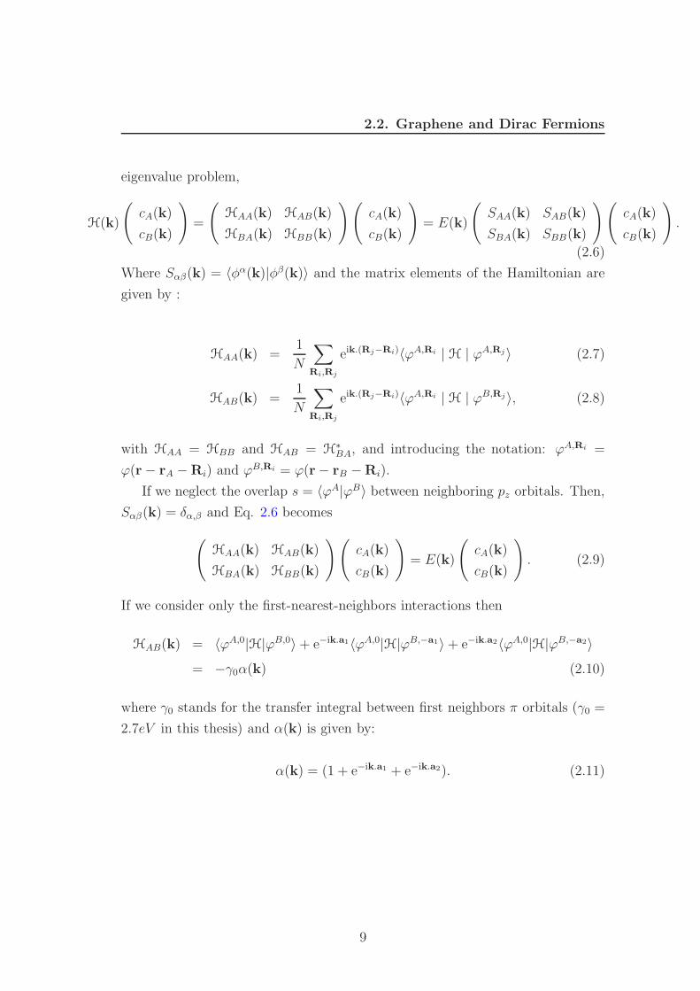
2.3 Band structure of graphene (a), the zoom-in figure at close to K
and K ′ points (b,c) and the density of state of graphene. (Fig. is
taken from [2]) . . . . . . . . . . . . . . . . . . . . . . . . . . . . 10
2.4 Some kinds of sp3 disorder in graphene . . . . . . . . . . . . . . . 15
2.5 The contribution from intra and intervalley scattering (Fig. is
taken from [3]) . . . . . . . . . . . . . . . . . . . . . . . . . . . . 15
2.6 Magnetoconductance for W = 2γ0 (top panels) and W = 1.5γ0
(bottom panels), the data is extracted from theoretical (left panels)
and experimental (right panels) study (Fig. is taken from [4]) . . 16
2.7 The electronic band structure and projected density of states in
the vicinity of the band gap for graphane (a) and fluorographene
(b) (Fig. is taken from [5]) . . . . . . . . . . . . . . . . . . . . . . 17
2.8 Elastic scattering time (τe) versus energy for three different long-
range potential strengths W. Left inset: τe for various densities of
epoxide defects. Right inset: τe for various densities of hydrogen
defects (Fig. is taken from [4]) . . . . . . . . . . . . . . . . . . . . 19
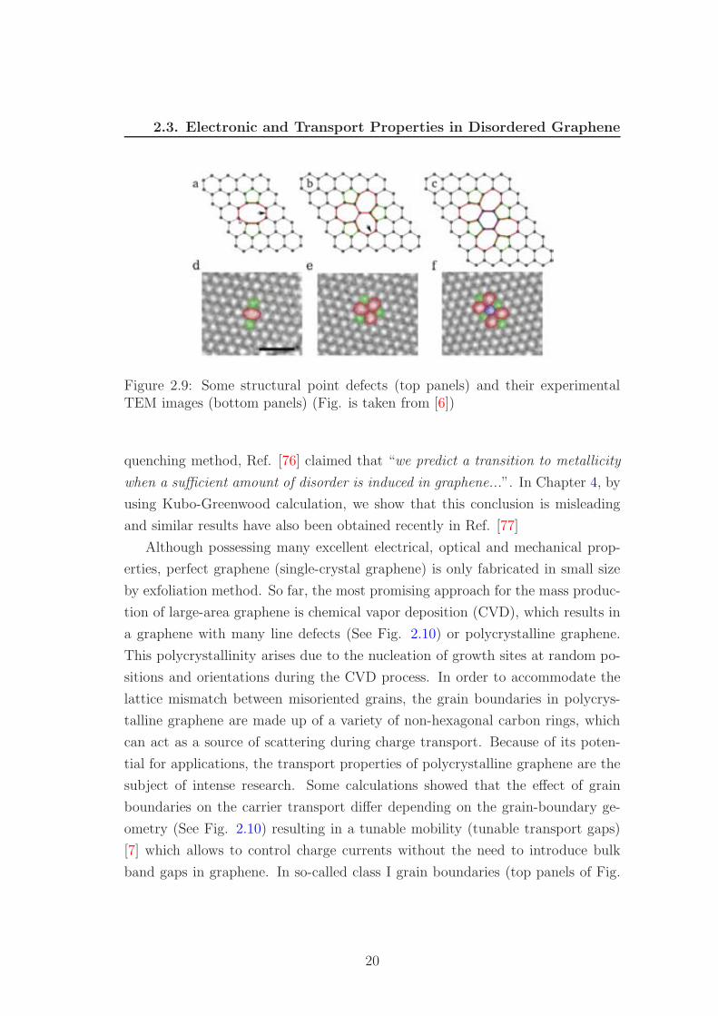
2.9 Some structural point defects (top panels) and their experimental
TEM images (bottom panels) (Fig. is taken from [6]) . . . . . . . 20
viii
LIST OF FIGURES
2.10 Two classes of electron transport through grain boundaries (Fig.
is taken from [7]) . . . . . . . . . . . . . . . . . . . . . . . . . . . 21
2.11 Spin-orbit coupling in graphene: a) Intrinsic SOC forces. b) Rashba
SOC force . . . . . . . . . . . . . . . . . . . . . . . . . . . . . . . 25
2.12 Electronic bandstructure of graphene with SOC (Figure is taken
from [8]) . . . . . . . . . . . . . . . . . . . . . . . . . . . . . . . . 28
2.13 Two possible hopping paths through s and p orbitals (top panels)
and through d orbital (bottom panels) lead to the first and the
second terms, respectively in Eq. (2.47) (Figure is taken from [9]) 30
2.14 A representative hopping path is responsible for Rashba SOC in
Eq. (2.48) (Figure is taken from [9]) . . . . . . . . . . . . . . . . . 31
2.15 DP spin relaxation in graphene: (a) Dirac coin when SOC is in-
cluded. (b) B‖(k) along the Fermi circle. (c) Charged impurities
in substrate induce electric field in graphene. (d) Illustration of the
spin relaxation in a spatially random potential due to the charged
carriers. (f) Calculated spin relaxation time τs as a function of the
Fermi energy Ef . (Figure is taken from [10]) . . . . . . . . . . . . 35
2.16 Sketch of scattering by a potential U(r) in the chiral channels
(Figure is taken from [11]) . . . . . . . . . . . . . . . . . . . . . . 37
3.1 Three transport regimes. (Fig. is taken from [12]) . . . . . . . . . 44
3.2 Diffusion coefficient (main frame) and displacement (inset) in three
transport regimes: (a) Ballistic regime, (b) Diffusive regime and
(c) Localized regime . . . . . . . . . . . . . . . . . . . . . . . . . 50
3.3 Illustration of the time dependence of diffusion coefficient D(E, t) 52
3.4 The application of Kubo formalism in real space: Velocity and
density of states for pristine graphene. . . . . . . . . . . . . . . . 56
3.5 The visualization of real space method in polycrystalline graphene.
a) Small portion of a polycrystalline graphene sample. b)-d) Time
evolution of a wave packet within the sample. . . . . . . . . . . . 57
3.6 Spherical coordinate system for spin . . . . . . . . . . . . . . . . . 59
4.1 The observation of ZEMs (Figure is taken from Ref. [13]) . . . . . 64
ix
LIST OF FIGURES
4.2 Main frame: Conductivity of graphene with n=0.8% (compensated
case): semiclassical value σsc (solid line), σmin = 4e2/πh (dotted
line) and Kubo conductivity at various time scales. Left inset:
DOS for varying vacancy density, together with the pristine case
(dashed line). Right inset: Mean free paths for n = 0.1%; 0.2%;
0.4%. . . . . . . . . . . . . . . . . . . . . . . . . . . . . . . . . . . 67
4.3 Length-dependent conductivity for different energies and 0.8% va-
cancy concentration in the compensated case. (a) Conductivity σ
and quantum correction δσ = σ − σsc at E = 0.4 eV. The loga-
rithmic fit confirms the weak-localization regime. (b) Low energy
conductivity (E = 0.2 eV) and corresponding fit indicate Ander-
son localization regime. (c) At zero energy the conductivity decay
is even stronger and cannot be fitted with an exponential decay.
(d) Conductivity at largest simulated times (8.2ps) and its residual
dependence on η. . . . . . . . . . . . . . . . . . . . . . . . . . . . 70
4.4 Main frame: σsc(E) and σ(E, t) for graphene (uncompensated
case) and energy resolution η = 3 meV. Left inset: DOS with
energy gap revealed by η scaling and ZEMs. Right inset: Diffu-
sion coefficients at E = 0.5 eV and E = 0 (η = 3 meV) for both
compensated (AB) and uncompensated (AA) cases. All data for
n = 0.8% . . . . . . . . . . . . . . . . . . . . . . . . . . . . . . . . 71
4.5 Main frame: Conductivity for strips with W = 150 nm, L = 15
nm and compensated vacancy density up to 2%. Inset: Same
information for uncompensated vacancies with densities up to 1%. 73
4.6 Main frame: Average conductivity peak versus n for strips with
W = 150 nm and L = 5, 10 and 15 nm. The shaded areas around
the curves indicate the standard deviation with respect to the av-
erage value. Top inset: Same as main frame but as a function of
n×L2. The thick straight line is a guide to the eye. Bottom inset:
Average conductivity for W = 150 nm, L = 15 nm and various n. 75
x
LIST OF FIGURES
4.7 (a) Extrinsic DOS for compensated vacancies as a function of the
energy; (b) Same as (a) for uncompensated vacancies; (c) Esti-
mation of the gap width and its fit as a function of the density of
uncompensated vacancies. . . . . . . . . . . . . . . . . . . . . . . 77
4.8 Structure and morphology of GGBs by theory, TEM, and STM/AFM.
a) Top panel; 5-7 GGB between two graphene grains with a misori-
entation angle of 21.8o . Bottom panel; TEM image [14] of a thin
5-7 GGB between grains with a misorientation angle of 27o. Re-
produced with permission. [14] Copyright 2011, Nature Publishing
Group. b) Left panel; simulated construction of a disordered GGB,
including a range of non-hexagonal rings and carbon vacancies. [15]
Right panel; STM image of a disordered GGB revealing a similar
morphology to the simulated one. Reproduced with permission.
[16] Copyright 2012, AIP Publishing. c) Top panel; 3D morphol-
ogy of a 5-7 GGB, indicating out of plane relaxation. [17] Bottom
panels; buckled AFM morphology of polycrystalline graphene af-
ter UV exposure. Position 2 indicates out of plane buckling at
the GGB. [18] Reproduced with permission. [18] Copyright 2012,
Nature Publishing Group. d) The simulated patterns and STM
images of two merged grains with identical orientation on a BN
substrate (top panels) and a Ni substrate (bottom panels). [19, 20]
No GGB is observed on the BN substrate, while a 5-8-5 GGB line
appears on the Ni substrate. Reproduced with permission. [19, 20]
Copyright 2013 and 2010, Nature Publishing Group. . . . . . . . 80
4.9 TEM approach to identifying graphene grain orientations. a) an
electron diffraction pattern arising from two misoriented grains. b)
Mapping of several grains with different orientations. Reproduced
with permission. [21] Copyright 2011, ACS Publishing. . . . . . . 84
xi
LIST OF FIGURES
4.10 Liquid crystal coating approach to identifying graphene grain ori-
entations. a) The hexagonal rings of LC molecules align coherently
with hexagonal rings in graphene. Reproduced with permission.
[22] Copyright 2012, Nature Publishing Group. b) POM images of
LC molecules aligned on each graphene grain, revealing a strong
optical contrast between misoriented grains. . . . . . . . . . . . . 85
4.11 UV treatment approach to identifying graphene grain orientations.
a) Principle of GGB visualization by UV treatment. b-c) Selective
oxidation of an underlying the copper substrate for direct optical
identification (b) of the GGBs, confirmed by AFM (c). Reproduced
with permission. [18] Copyright 2012, Nature Publishing Group. 87
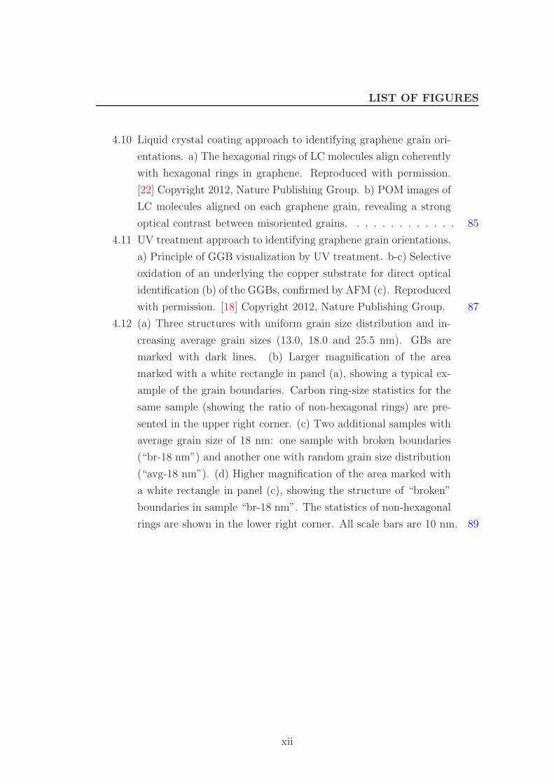
4.12 (a) Three structures with uniform grain size distribution and in-
creasing average grain sizes (13.0, 18.0 and 25.5 nm). GBs are
marked with dark lines. (b) Larger magnification of the area
marked with a white rectangle in panel (a), showing a typical ex-
ample of the grain boundaries. Carbon ring-size statistics for the
same sample (showing the ratio of non-hexagonal rings) are pre-
sented in the upper right corner. (c) Two additional samples with
average grain size of 18 nm: one sample with broken boundaries
(“br-18 nm”) and another one with random grain size distribution
(“avg-18 nm”). (d) Higher magnification of the area marked with
a white rectangle in panel (c), showing the structure of “broken”
boundaries in sample “br-18 nm”. The statistics of non-hexagonal
rings are shown in the lower right corner. All scale bars are 10 nm. 89
xii
LIST OF FIGURES
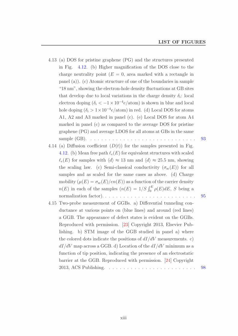
4.13 (a) DOS for pristine graphene (PG) and the structures presented
in Fig. 4.12. (b) Higher magnification of the DOS close to the
charge neutrality point (E = 0, area marked with a rectangle in
panel (a)). (c) Atomic structure of one of the boundaries in sample
“18 nm”, showing the electron-hole density fluctuations at GB sites
that develop due to local variations in the charge density δi: local
electron doping (δi < −1×10⁻⁴e/atom) is shown in blue and local
hole doping (δi > 1×10⁻⁴e/atom) in red. (d) Local DOS for atoms
A1, A2 and A3 marked in panel (c). (e) Local DOS for atom A4
marked in panel (c) as compared to the average DOS for pristine
graphene (PG) and average LDOS for all atoms at GBs in the same
sample (GB). . . . . . . . . . . . . . . . . . . . . . . . . . . . . . 93
4.14 (a) Diffusion coefficient (D(t)) for the samples presented in Fig.
4.12. (b) Mean free path ℓe(E) for equivalent structures with scaled
ℓe(E) for samples with 〈d〉 ≈ 13 nm and 〈d〉 ≈ 25.5 nm, showing
the scaling law. (c) Semi-classical conductivity (σsc(E)) for all
samples and as scaled for the same cases as above. (d) Charge
mobility (µ(E) = σsc(E)/en(E)) as a function of the carrier density
n(E) in each of the samples (n(E) = 1/S∫ E
0ρ(E)dE, S being a
normalization factor). . . . . . . . . . . . . . . . . . . . . . . . . . 95
4.15 Two-probe measurement of GGBs. a) Differential tunneling con-
ductance at various points on (blue lines) and around (red lines)
a GGB. The appearance of defect states is evident on the GGBs.
Reproduced with permission. [23] Copyright 2013, Elsevier Pub-
lishing. b) STM image of the GGB studied in panel a) where
the colored dots indicate the positions of dI/dV measurements. c)
dI/dV map across a GGB. d) Location of the dI/dV minimum as a
function of tip position, indicating the presence of an electrostatic
barrier at the GGB. Reproduced with permission. [24] Copyright
2013, ACS Publishing. . . . . . . . . . . . . . . . . . . . . . . . . 98
xiii
LIST OF FIGURES
4.16 Principle of four-probe measurement applied to GGBs. A serie of
Hall bars is fabricated across the GGB region. The resistivity of
the GGBs can be extracted from this measurement set-up. Intra-
grain resistances RL and RR are subtracted from the inter-grain
resistance to obtain RB , the resistance of the GGB. . . . . . . . 100
4.17 Four-probe measurement of GGBs. a) Example of a four-probe
setup for measuring the resistivity of a GGB. b) I−V curves mea-
sured within individual grains (red and blue curves) and across
the GGB (green curve). The reduced slope for the inter-grain
measurement indicates extra resistance contributed by the GGB.
Reproduced with permission. [25] Copyright 2011, Nature Pub-
lishing Group. c) Four-probe measurement setup mounted on a
TEM holder, where individual graphene grains are identified in
the red and blue regions. d) Top plot; four-probe measurements of
the inter- and intra-grain resistance as a function of gate voltage
(black and gray curves, respectively). Bottom plot; the extracted
GB resistivity as a function of gate voltage in volt. Reproduced
with permission. [26] Copyright 2013, AAAS. . . . . . . . . . . . 102
4.18 Principle of the scaling law to extract the GGB resistivity. a)
Derivation of the ohmic scaling law. b)-c) Sheet resistance mea-
surements of graphene with small and large grain sizes. d) Extrac-
tion of GGB resistivity by fitting the scaling law to sheet resistance
measurements. . . . . . . . . . . . . . . . . . . . . . . . . . . . . 104
4.19 Global measurements from scaling law. a) Sheet resistance of poly-
crystalline graphene as a function of average grain size. Grain sizes
were determined via Raman spectroscopy. Reproduced with per-
mission. [27] Copyright 2011, IOP Publishing. b) Another example
of the scaling behavior of polycrystalline graphene. The dotted line
represents a fit to the scaling law described in the main text. Re-
produced with permission. [18] Copyright 2012, Nature Publishing
Group. . . . . . . . . . . . . . . . . . . . . . . . . . . . . . . . . 105
xiv
LIST OF FIGURES
4.20 Chemical reactivity of GGBs by experiments. a) Representation
of selective chemical functionalization of GGBs. b) The location
of GGBs can be imaged with AFM after burning them away at
high temperature, which highlights their selective oxidation. Re-
produced with permission. [28] Copyright 2011, AIP Publishing.
c) An optical image of polycrystalline graphene indicates the selec-
tive oxidation of an underlying copper substrate below the GGBs.
d) Raman spectroscopy indicates the strong oxidation at the GGBs
after UV treatment. e)-f) Raman mapping indicates strong oxida-
tion of the GGBs (D-band), as well as strain due to the expansion
of the oxidized copper substrate below the GGBs (G and G′ band
shifts). Reproduced with permission. [18] Copyright 2012, Nature
Publishing Group. . . . . . . . . . . . . . . . . . . . . . . . . . . 107
4.21 Optical image of the four-probe device across a GGB. a) E-beam
lithography resist (PMMA) location at a merging region including
a GGB. b)-c) A final device with Hall bar geometry at merging
region of two graphene domains. . . . . . . . . . . . . . . . . . . 109
4.22 O2 Selective functionalization of GGBs by UV treatment under
environment.a)-b) Effect of annealing at 250oC in 3h. Funtional
groups are removed from a GGB. c)-d) Effect of UV treatment
under O2 environment. The exclusive change of the inter-grain
resistance indicates selective functionalization at the GGB. The
UV treatment is saturated after 1 minute of UV treatment. . . . 111
4.23 Simulation of the effect of functional groups at GGBs. a)-b) Schematic
of GGBs functionalized by H and OH groups, respectively. c) De-
pendence of the resistivity of GGBs on functional groups with var-
ious concentrations. d) Summary of experimental and simulated
results for the resistivity of GGBs. . . . . . . . . . . . . . . . . . 113
xv
LIST OF FIGURES
4.24 (a) Schematic of the dual-gate GFET, consisting of a poly-G chan-
nel on top of an insulator layer, which is grown on a heavily-doped
Si wafer acting as the back gate. An artistic view of the patchwork
of coalescing graphene grains of varying lattice orientations and
size is shown in (b). The source and drain electrodes contact the
poly-G channel from the top and are assumed to be ohmic. The
source is grounded and considered the reference potential in the
device. The electrostatic modulation of the carrier concentration
in graphene is achieved via a top-gate stack consisting of the gate
dielectric and the gate metal. . . . . . . . . . . . . . . . . . . . . 119
4.25 Quantum capacitance (a) and density of states (b) of polycrys-
talline graphene considering different average grain sizes. The PG
case has also been plotted for the sake of comparison. . . . . . . 121
4.26 Transfer characteristics (a) and transconductance (c) of the graphene
field-effect transistor considering different samples of polycrystalline
graphene as the active channel. (b) Estimated low-field carrier mo-
bility as a function of the carrier density for each of the samples. 122
4.27 Output characteristics (a) and output conductance (b) of the graphene
field-effect transistor considering different samples of polycrystalline
graphene as the active channel. . . . . . . . . . . . . . . . . . . . 123
4.28 Intrinsic gain as a function of the drain voltage. The transconduc-
tance and output conductance are also plotted at Vgs = 0.25V . . 124
4.29 Intrinsic maximum and cutoff frequency for the simulated transis-
tor assuming a channel length of 100nm. . . . . . . . . . . . . . 125
4.30 (a) and (b) show details of amorphous graphene samples S1 and
S2, respectively, used to compute the conductivity with the Kubo
approach. (c) Total density of states of the two amorphous sam-
ples. The prisitine crystalline graphene case (dashed lines) is also
shown for comparison. . . . . . . . . . . . . . . . . . . . . . . . . 128
4.31 Normalized time-dependent diffusion coefficients for two selected
energies for both samples S1 and S2. Inset: localization lengths as
a function of the carrier energy . . . . . . . . . . . . . . . . . . . 131
xvi
LIST OF FIGURES
4.32 Elastic mean free path versus energy for the two samples. DOS of
sample S1 is also shown for comparison in rescaled units. Inset:
semiclassical conductivity of corresponding lattices. . . . . . . . . 132
4.33 Landauer-Buttiker conductance (for W=11.4 nm) of two amor-
phous ribbons contacted to graphene electrodes with L = 1.6 and
8.6 nm, respectively. The conductance of a pristine graphene con-
tact with the same lateral size (11.4 nm) is shown for comparison.
The inset shows the dependence of the conductivity on the ribbon
size L; symbols: calculated points; line: fit to σ(L) ∼ LWe−L/ξ . . . 133
5.1 Spin Dynamics in disordered graphene. (a) Ball-and-stick model
of a random distribution of adatoms on top of a graphene sam-
ple (b) Top view of the gold adatom sitting on the center of
an hexagon (c),(d) Time-dependent projected spin polarization
Sz(E, t) of charge carriers (symbols) initially prepared in an out-
of-plane polarization (at Dirac point (red curves) and at E = 150
meV (blue curves)). Analytical fits are given as solid lines (see
text). Parameters are VI = 0.007γ0, VR = 0.0165γ0, µ = 0.1γ0,
ρ = 0.05% (c) and ρ = 8% (d). . . . . . . . . . . . . . . . . . . . . 139
5.2 Spin relaxation times and transport mechanisms. Spin relaxation
times (τs) for ρ = 0.05% (a) and ρ = 8% (b). Black (red) solid
symbols indicate τs for µ = 0.1γ0 (µ = 0.2γ0). TΩ vs. E is also
shown (open symbols). τp (dotted line in (b)) is shown over a wider
energy range (top x-axis) in order to stress the divergence around
E = 0 (µ = 0.2γ0). We cannot evaluate τp below 100 meV, since
the diffusive regime is not established within our computational
reach. Panels (c) and (d): Time dependent diffusion coefficient
D(t) for ρ = 0.05% and ρ = 8% with µ = 0.2γ0. . . . . . . . . . . 142
xvii
LIST OF FIGURES
5.3 Spin relaxation times deduced from the continuum and microscopic
models. (a) Spin relaxation times (τs) for varying ρ between 0.05%
and 8% extracted from the microscopic model (with µ = 0.1γ0).
Inset: τs values using the continuum model for ρ = 1% and 8%
(filled symbols). A comparison with the microscopic model (with
µ = 0) is also given for ρ = 8% (open circles). (b) Scaling behavior
of TΩ and τs versus 1/ρ. The TΩ values obtained with the micro-
scopic (resp. continuum) model are given by red diamonds (resp.
red solid lines). τs values for the microscopic model (blue squares)
and the continuum model (black circles) are shown for two selected
energies E = 150meV (solid symbols) and E = 0 (open symbols).
Solid lines are here guides to the eye. . . . . . . . . . . . . . . . . 145
5.4 Spin and pseudospin dynamics in graphene with ρ = 8% of adatoms.
Time dependence of spin-polarization Sz (blue) and pseudospin po-
larization σz (green) in z projection for energies E = 130meV (a),
E = 0 (b), and E = −5 meV (c). Note that all quantities are
normalized to their maximum value to better contrast them in the
same scale. Middle panels show the time evolution for both spin
(from blue to pink) and pseudospin (from green to orange). The
snapshots are taken at different times from t1 to t4 sampling the
shaded regions in (a), (b), (c). (d) Fourier transform of Sz(t) plot-
ted over oscillation period, and showing non-dispersive spectra at
high energy (between E =125 meV, 130 meV and 135 meV). Low-
energy spectra (for E = −5 meV, 0 and 5 meV) change strongly
with energy (dispersive) showing a gradual reduction and blue shift
of the original Rashba peak at about 0.19 ps and the appearance
of additional features. . . . . . . . . . . . . . . . . . . . . . . . . 146
5.5 Band structure calculated using the Kane-Mele-Rashba model for
8% adatom concentration. The inset shows the typical Rashba-like
spin texture for the conduction bands. . . . . . . . . . . . . . . . 149
xviii
LIST OF FIGURES
5.6 Energy dependence of the spin polarization vector |~S| for states in
the two conduction bands obtained with the 4-bands low-energy
model. The results correspond to adatom concentration 8% (1/4
ML) (left pannel) and 25% (right pannel). In both cases, close to
the Dirac point, spin and pseudospin entanglement is very high
given the small values of |~S| ≪ 1. . . . . . . . . . . . . . . . . . . 151
5.7 Time-dependence of the modulus of the spin polarization vector
|~S(E, t)| in the microscopic model with realistic disorder and gold
ad-atom concentrations 0.05% and 8% at two specific energies:
Dirac point E = 0 and E = 150 meV. . . . . . . . . . . . . . . . . 153
5.8 (a) Ball-and-stick model of a graphene substrate with randomly
adsorbed thallium atoms (concentration is 15%). (b) Same as (a)
but with adatoms clustered in islands with a radius distribution
varying up to 3 nm (histogram shown in (d)). (c) Zoom-in of a
typical thallium ad-atoms-based island. All thallium atoms are
positioned in the hollow position and equally connected to the 6
carbon atoms forming the hexagon underneath (following [29]). . . 159
5.9 (a) Differential conductance for an armchair ribbon of width W=50
nm with a concentration n=15% of randomly scattered thallium
adatoms over a section with length L=50 nm. The potential energy
on the contacts is set to V=-2.5 eV. The presence of long-range
disorder with ∆ up to 1 eV is taken into account. (b) Local density-
of-occupied-states for spin down electrons injected from the right
contact for ∆ = 0 at energy E=-100 meV, see the arrow in (a).
(c) Same as (b) but for spin up electrons. . . . . . . . . . . . . . . 163
5.10 (a) Differential conductance for an armchair ribbon of width W=50
nm with a concentration n=15% of clustered thallium adatoms (in
islands with radius r up to 2-3 nm) over a section with length L=50
nm. The potential energy on the contacts is set to V=-2.5 eV. (b)
Local density-of-occupied-states in the case r ∈ [2, 3] nm, for spin
down electrons injected from the right contact at energy E=-100
meV, see the arrow in (a). (c) Same as (b) but for spin up electrons.164
xix
LIST OF FIGURES
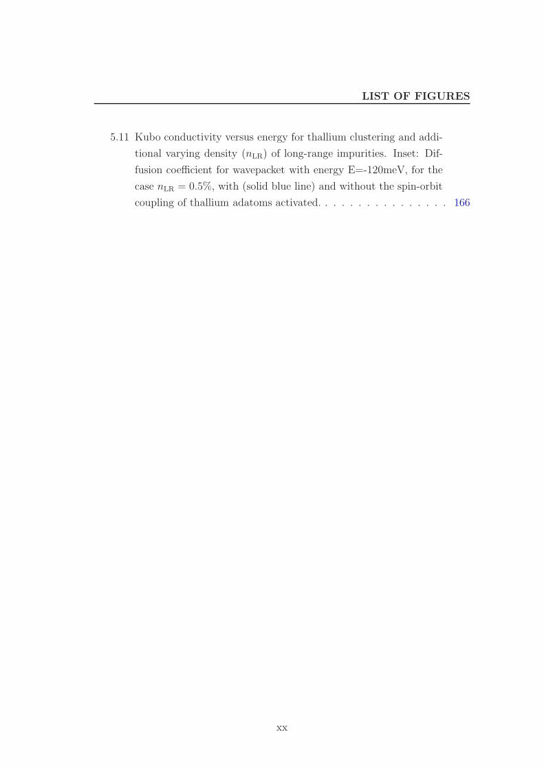
5.11 Kubo conductivity versus energy for thallium clustering and addi-
tional varying density (nLR) of long-range impurities. Inset: Dif-
fusion coefficient for wavepacket with energy E=-120meV, for the
case nLR = 0.5%, with (solid blue line) and without the spin-orbit
coupling of thallium adatoms activated. . . . . . . . . . . . . . . . 166
xx
Chapter 1
Introduction
Graphene, an atomic monolayer of carbon atoms arranged into a honeycomb
lattice, is a fascinating and unique system. It is an extreme 2D condensed matter
system where the charge carrier dynamics can be described as quasi-relativistic
particles with zero effective carrier mass and the transport properties are governed
by the Dirac equation, whereby their mobilities have unprecedentedly large values.
Many of the interesting properties in graphene result from these characteristics
which are analogous to those of relativistic, massless fermions. During the past
ten years after its discovery, graphene has attracted a great attention. Ever since,
numerous unique electrical, optical, and mechanical properties of graphene have
been discovered such as optical transparence, high strength and stiffness, Klein
tunneling, half-integer quantum Hall effect, weak antilocalization, etc. However,
disorders are unavoidable factors that affect transport properties of graphene
and it is crucial to study their detrimental effects to have a comprehension of real
graphene sample.
Moreover, in order to develop technology and application based on graphene
the integration of the material at wafer scale is mandatory. The chemical va-
por deposition (CVD) growth technique is the best candidate for achieving a
combination of high structural quality and wafer-scale growth. However, the
resulting CVD graphene is polycrystalline graphene [30, 31, 32, 33], formed by
many single-crystal grains with different orientations [14]. In order to accom-
modate the lattice mismatch between misoriented grains, the grain boundaries
in polycrystalline graphene are made up of a variety of non-hexagonal carbon
1
1. Introduction
rings, which can act as a source of scattering during charge transport. The prop-
erties of polycrystalline graphene are therefore dictated by their grain size and
by the atomic structure at the grain boundaries. Effects of structural defects
on the electronic, mechanical and transport properties of graphene have recently
been analyzed theoretically [34, 4]. Moreover, several theoretical studies have
reported on the effect of a single GB on electronic [35, 7], magnetic [36], chem-
ical [37], and mechanical [17, 38, 39] properties of graphene. However, very few
studies [37, 39] have discussed more complex forms of GBs (not restricted to
infinite linear arrangements of dislocation cores), which would better correspond
to the experimentally observed structures [14, 21, 40]. Furthermore, because of
experimental challenges only a few experimental works [25] have systematically
investigated the impact of grain boundaries on electronic transport, mainly con-
firming the reduced conductivity as compared to single-crystalline samples. Very
recent electrical measurements on individual grain boundaries in CVD-graphene
also reported that a good interdomain connectivity is a fundamental geometri-
cal requirement for improved transport capability [26]. However, to date little is
known about the global contribution of complex distributions of GBs to measured
charge mobilities [41]. Therefore, to understand the large-scale electrical trans-
port properties of polycrystalline graphene, it is important to perform a detailed
exploration of the role played by the grain boundaries.
In regards to the potential of graphene for spintronics, the extremely small in-
trinsic spin-orbit coupling (SOC) of graphene and the lack of hyperfine interaction
with the most abundant carbon isotope have led to intense research into possible
applications of this material in spintronic devices with the anticipated possibility
of transporting spin information over very long distances [42, 10, 43]. However,
the spin relaxation times are still found to be orders of magnitude smaller than
initially predicted [44, 45, 46, 47, 48], while the major physical process for spin
equilibration and its dependence on charge density and disorder remain elusive.
Experiments have been analyzed in terms of the conventional Elliot-Yafet and
Dyakonov-Perel processes, yielding contradictory results. Recently, a mechanism
based on resonant scattering by local magnetic moments has also been proposed
[49] but contains too many free parameters and do not solve the controversial
results reported experimentally [50].
2
1. Introduction
In 2005, the quantum spin Hall state was predicted in graphene by Kane
and Mele [51]. The Kane and Mele model is two copies of the Haldane model
[52] such that the spin up electron exhibits a chiral integer quantum Hall effect
while the spin down electron exhibits an anti-chiral integer quantum Hall effect.
This novel electronic state of matter is gapped in the bulk and supports the
transport of spin and charge in gapless edge states that propagate at the sample
boundaries. The edge states are insensitive to disorder (which does not break time
reversal symmetry) because their directionality is correlated with spin. However,
this beautiful state is unobservable in graphene due to weak spin-orbit coupling
in intrinsic graphene. A solution for this problem is endowing graphene with
certain heavy adatoms such as thallium or indium [29], but to date the clustering
effect of these adatoms make the quantum spin Hall state seem to jeopardize its
observation.
The purpose of this thesis is to address above problems. The thesis is orga-
nized into 6 chapters and 2 appendices. The contents are developed as follows:
Chapter 1 gives the purpose of this thesis and overviews the problems of
interest. The content of each chapter in this thesis is also mentioned in this
introductory Chapter.
Chapter 2 presents the electronic and transport properties of clean graphene.
In this Chapter the linear band structure of graphene is derived, some special
characteristics of Dirac fermions such as chirality, zero effective mass, etc. are
mentioned. The Chapter also covers the literature of electronic transport and
spin transport in graphene. In this later part, spin-orbit interactions are derived
and their modifications on the Dirac band structure are reviewed. The final part
of this Chapter is devoted to a discussion on the discrepancy of experimental and
theoretical results concerning spin relaxation in graphene. Two mechanisms for
spin relaxation in graphene, Elliot-Yafet and Dyakonov-Perel, are also derived.
Chapter 3 briefly overviews the Kubo-Greenwood transport formalism which
is extensively used in this thesis. In this Chapter, two different approaches are
discussed namely, the semiclassical and quantum approaches, which lead to the
Einstein relation for conductivity. The real space transport method for the Kubo
conductivity calculation is also introduced. An extension of real space order O(N)
transport formalism is developed to study spin transport in the realistic system.
3
1. Introduction
Chapter 4 focuses on the electronic transport properties of disordered graphene.
The transport properties are studied with gradually increasing disorder, from
point defects in graphene with vacancies to line defects in polycrystalline graphene
and finally to the extremely disordered form of graphene, amorphous membranes
of sp2 graphene. The studies are systematically concentrated on different aspects
of graphene in perspectives of applications.
Chapter 5 deals with the graphene spin relaxation problems. In this Chapter
we point out the limitations of Elliot-Yafet and Dyakonov-Perel mechanisms for
graphene, and we propose a new mechanism driven by the entanglement between
spin and pseudospin quantum degree of freedoms which governs the fast spin re-
laxation close to Dirac point in graphene. At the final of this Chapter, we explain
the difficulty of observing quantum spin Hall effect in graphene when depositing
heavy adatoms. The natural clustering trend of such adatoms weaken the spin-
orbit coupling effect which is a crucial factor of the formation of topological edge
state. The Chapter also reports the formation of a robust metallic state which is
related to the enhanced percolation of propagating states between islands.
Chapter 6 summarizes the thesis and suggests some opening directions for the
near future.
4
Chapter 2
Electronic and Transport
Properties of Graphene
2.1 Introduction
Graphene has received a great attention since it was first isolated by Nobel Lau-
reates Konstantin Novoselov and Andre K. Geim in 2004. The reason for such
excitement is that graphene is the first truly 2D crystal ever observed in nature
and possesses remarkable electrical, chemical and mechanical properties. Fur-
thermore, electrons in graphene show quasi-relativistic behavior, and the system
is therefore an ideal candidate for the test of quantum field-theoretical models
that have been developed in high-energy physics. Most prominently, electrons in
graphene may be viewed as massless charged fermions existing in 2D space, par-
ticles that one usually do not encounter in our three-dimensional world. Indeed,
all massless elementary particles, such as photons or neutrinos, happen to be
electrically neutral. Graphene is therefore an exciting bridge between condensed
matter and high-energy physics, and the research on its electronic properties
unites scientists with various thematic backgrounds.
Graphene is also an attractive material for spintronics due to the theoretical
possibility of long spin lifetimes arising from low intrinsic spin-orbit coupling and
weak hyperfine interaction [53]. However, Hanle spin precession mesurements
and non-local spin valve geometry have reported spin lifetimes that are orders of
5
2.2. Graphene and Dirac Fermions
magnitude shorter than expected theoretically [44, 54, 55, 56]. Several studies
have investigated spin relaxation including the roles of impurity scattering [56]
and graphene thickness [57] and specially, ferromagnet contact-induced spin re-
laxation was predicted to be responsible for the short spin lifetimes observed in
experiments [58]. However, these explanations haven’t given a satisfying answer
for the dicrepancy between theoretical results and experimental data. This has
prompted theoretical studies of the extrinsic sources of spin relaxation such as
impurity scattering [59], ripples [53], and substrate effects [10] but the problem
is still puzzling and unsolved.
In this chapter we will briefly review some theoretical and experimental results
about fundamental electric and spin transport properties of graphene. Firstly, we
will derive graphene band structure and massless Dirac equation for graphene in
Section 2.2. Next, some experimental and theoretical studies about transport
properties of graphene are discussed in Section 2.3. Section 2.4 discusses some
aspects of spin-orbit coupling in graphene which plays an important role for
studying spin relaxation in Chapter 5.
2.2 Graphene and Dirac Fermions
The most interesting property of graphene might be the Dirac-cone energy dis-
persion. This is the consequence of sp2 hybridization and graphene symmetry.
In this Section, I briefly review its structure, the commonly used tight-binding
description and the deviation of the linear energy dispersion of graphene.
2.2.1 Graphene
Graphene is a single atomic layer of graphite, an allotrope of carbon that is made
up of very tightly bonded carbon atoms organised into a hexagonal lattice. What
makes graphene so special is its sp2 hybridization and very thin atomic thickness
(see Fig. 2.1). These properties are what enable graphene to break so many
records in terms of strength, electricity, heat conduction, etc.
Carbon is a common element in the nature, with atomic number 6, group 14
on the periodic table. The electronic configuration of carbon is 1s22s22p2 which
6
2.2. Graphene and Dirac Fermions
σ
σ
σ
σ
π*
σ*
π
E (eV)
+8
-4
+12
-8
π
π
EF
(a) (b)
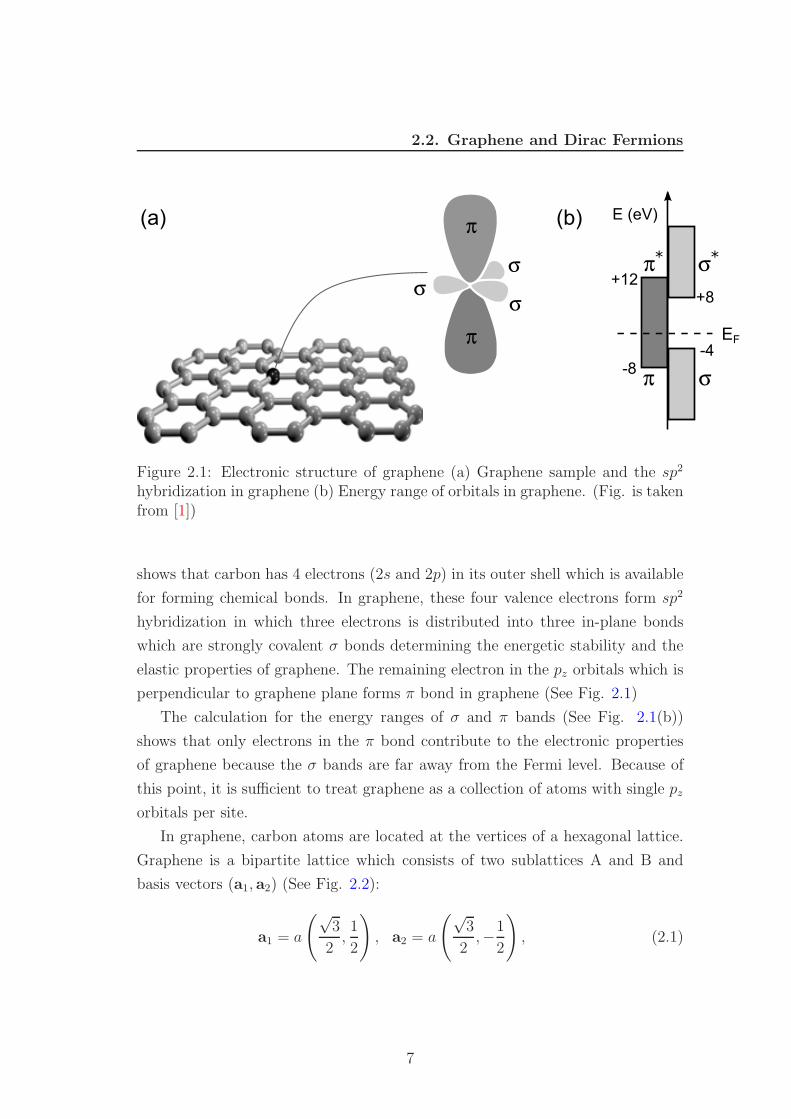
Figure 2.1: Electronic structure of graphene (a) Graphene sample and the sp2
hybridization in graphene (b) Energy range of orbitals in graphene. (Fig. is takenfrom [1])
shows that carbon has 4 electrons (2s and 2p) in its outer shell which is available
for forming chemical bonds. In graphene, these four valence electrons form sp2
hybridization in which three electrons is distributed into three in-plane bonds
which are strongly covalent σ bonds determining the energetic stability and the
elastic properties of graphene. The remaining electron in the pz orbitals which is
perpendicular to graphene plane forms π bond in graphene (See Fig. 2.1)
The calculation for the energy ranges of σ and π bands (See Fig. 2.1(b))
shows that only electrons in the π bond contribute to the electronic properties
of graphene because the σ bands are far away from the Fermi level. Because of
this point, it is sufficient to treat graphene as a collection of atoms with single pz
orbitals per site.
In graphene, carbon atoms are located at the vertices of a hexagonal lattice.
Graphene is a bipartite lattice which consists of two sublattices A and B and
basis vectors (a1, a2) (See Fig. 2.2):
a1 = a
(√3
2,
1
2
)
, a2 = a
(√3
2,−1
2
)
, (2.1)
7
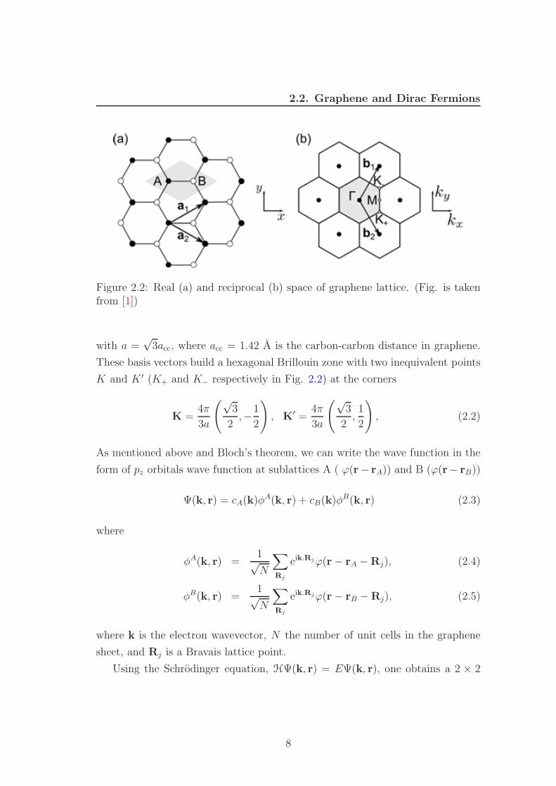
2.2. Graphene and Dirac Fermions
Figure 2.2: Real (a) and reciprocal (b) space of graphene lattice. (Fig. is takenfrom [1])
with a =√
3acc, where acc = 1.42 A is the carbon-carbon distance in graphene.
These basis vectors build a hexagonal Brillouin zone with two inequivalent points
K and K ′ (K+ and K− respectively in Fig. 2.2) at the corners
K =4π
3a
(√3
2,−1
2
)
, K′ =4π
3a
(√3
2,
1
2
)
, (2.2)
As mentioned above and Bloch’s theorem, we can write the wave function in the
form of pz orbitals wave function at sublattices A ( ϕ(r− rA)) and B (ϕ(r− rB))
Ψ(k, r) = cA(k)φA(k, r) + cB(k)φB(k, r) (2.3)
where
φA(k, r) =1√N
∑
Rj
eik.Rjϕ(r− rA −Rj), (2.4)
φB(k, r) =1√N
∑
Rj
eik.Rjϕ(r− rB −Rj), (2.5)
where k is the electron wavevector, N the number of unit cells in the graphene
sheet, and Rj is a Bravais lattice point.
Using the Schrodinger equation, HΨ(k, r) = EΨ(k, r), one obtains a 2 × 2
8
2.2. Graphene and Dirac Fermions
eigenvalue problem,
H(k)
(
cA(k)
cB(k)
)
=
(
HAA(k) HAB(k)
HBA(k) HBB(k)
)(
cA(k)
cB(k)
)
= E(k)
(
SAA(k) SAB(k)
SBA(k) SBB(k)
)(
cA(k)
cB(k)
)
.
(2.6)
Where Sαβ(k) = 〈φα(k)|φβ(k)〉 and the matrix elements of the Hamiltonian are
given by :
HAA(k) =1
N
∑
Ri,Rj
eik.(Rj−Ri)〈ϕA,Ri | H | ϕA,Rj〉 (2.7)
HAB(k) =1
N
∑
Ri,Rj
eik.(Rj−Ri)〈ϕA,Ri | H | ϕB,Rj〉, (2.8)
with HAA = HBB and HAB = H∗BA, and introducing the notation: ϕA,Ri =
ϕ(r− rA −Ri) and ϕB,Ri = ϕ(r− rB −Ri).
If we neglect the overlap s = 〈ϕA|ϕB〉 between neighboring pz orbitals. Then,
Sαβ(k) = δα,β and Eq. 2.6 becomes
(
HAA(k) HAB(k)
HBA(k) HBB(k)
)(
cA(k)
cB(k)
)
= E(k)
(
cA(k)
cB(k)
)
. (2.9)
If we consider only the first-nearest-neighbors interactions then
HAB(k) = 〈ϕA,0|H|ϕB,0〉 + e−ik.a1〈ϕA,0|H|ϕB,−a1〉 + e−ik.a2〈ϕA,0|H|ϕB,−a2〉= −γ0α(k) (2.10)
where γ0 stands for the transfer integral between first neighbors π orbitals (γ0 =
2.7eV in this thesis) and α(k) is given by:
α(k) = (1 + e−ik.a1 + e−ik.a2). (2.11)
9
2.2. Graphene and Dirac Fermions
Taking HAA(k) = HAA(k) = 0 as the energy reference, we can write H(k) as:
H(k) =
(
0 −γ0α(k)
−γ0α(k)∗ 0
)
. (2.12)
Diagonalizing this Hamiltonian gives the energy dispersion relations for π∗ (con-
duction) band (+) and π (valence) band (-) :
E±(k) = ±γ0|α(k)|= ±γ0
√
3 + 2 cos(k.a1) + 2 cos(k.a2) + 2 cos(k.(a2 − a1))
= ±γ0
√
1 + 4 cos
√3kxa
2cos
kya
24 cos2
kya
2. (2.13)
This band structure is plotted in Fig. 2.3 with the symmetry between the
Figure 2.3: Band structure of graphene (a), the zoom-in figure at close to K andK ′ points (b,c) and the density of state of graphene. (Fig. is taken from [2])
conduction band and the valence band which touch at three K and K ′ points
with zero density of state at this energy (Fig. 2.3(d)). Because of this, graphene
10
2.2. Graphene and Dirac Fermions
is called gapless semiconductor or semi-metal . In neutral graphene, the Fermi
level lie exactly at these points
2.2.2 Low-Energy Dispersion
Because of the fact that they can only experimentally tune the Fermi level a small
range (0.3eV) about the touching points, this is corresponding to a small variation
about the K and K ′ points in momentum space. Therefore, it is sufficient to
expand the energy dispersion in the vicinity of K and K ′ points by replacing
k → K(K′) + k which lets us write Eq. (2.12) in the form
H = ~vF (ησxkx + σyky). (2.14)
and Eq. (2.13) becomes
Es(k) = s~vF |k|, (2.15)
where vF =√
3γ0a/2~ is the electronic group velocity, η = 1(−1) for K(K ′)
points, s = ±1 is the band index (+1 for conduction band and -1 for valence
band) and the Pauli matrices are defined as usual:
σx =
(
0 1
1 0
)
, σy =
(
0 −ii 0
)
, σz =
(
1 0
0 −1
)
. (2.16)
Eq. (2.14) is almost the same the Dirac equation for the massless fermions
in quantum electrodynamics except from the fact that the Pauli matrices here
represent the sublattice degrees of freedom instead of spin and the speed of light
c is replaced by graphene velocity vF ≃ c/300. Therefore, the sublattice de-
grees of freedom and the touching points are called pseudospin and Dirac point,
respectively.
The linear energy dispersion in Eq. (2.15) leads to the fact that total density
of states is directly proportional to energy and carrier density is proportional to
energy squared.
11
2.2. Graphene and Dirac Fermions
Indeed,
ρ(E) =1
L2
∑
k
δ(E − E(k)) =
∫
gsgv2πkdk
(2π)2δ(E − E(k)) =
2|E|π~2v2F
(2.17)
which is plotted in Fig. 2.3(d), where gs = 2 and gv = 2 account for spin and
valley degeneracies, respectively. The carrier density is given by
n(E) =1
L2
∑
|k|≤kF
gsgv = gsgvk2F4π
=E2
π~2v2F(2.18)
To find the eigenstates of Dirac Hamiltonian (2.14), it is useful to write this
Hamiltonian in the term of momentum direction θk
Hη(k) = ~vFk
(
0 e−iηθk
e+iηθk 0
)
(2.19)
where θk = arctan(ky/kx). This Hamiltonian got the eigenvalues as in Eq. (2.15)
and the eigenfunctions
|Ψη,s(k)〉 =1√2
(
1
seiηθk
)
. (2.20)
Next, we are going to find eigenvalues of the helicity operator (an very important
feature of Dirac particle ) which here is defined as:
h = σ · p
|p| . (2.21)
where p = ~k is the electron momentum operator.
In order to do that, it is convenient to exchange the spinor components at the
K ′ point (for η = −1) [60],
|ΨK(k)〉 =
(
cA(k)
cB(k)
)
, |ΨK′
(k)〉 =
(
cB(k)
cA(k)
)
(2.22)
i.e., to invert the role of the two sublattices. In this case, the effective low-energy
12
2.2. Graphene and Dirac Fermions
Hamiltonian in Eq. (2.14) may be represented as
Hη(k) = η~vF (σxkx + σyky) = ~vF τ
z ⊗ ~σ~k. (2.23)
where τ are Pauli matrices represent the valley degree of freedoms called valley
pseudospin. Using Eq. (2.23) and Eq. (2.21)
Hη(k) = η~vFkh (2.24)
we find that helicity operator commutes with the Hamiltonian, the projection
of the pseudospin is a well-defined conserved quantity which can be either pos-
itive or negative, corresponding to pseudospin and momentum being parallel or
antiparallel to each other . The band index s, which describes the valence and
conduction bands, is therefore entirely determined by the chirality and the valley
pseudospin, and one finds
s = ηh (2.25)
which help us find out that chirality changes sign from conduction band to valence
band and from K to K ′ points. The fact that pseudospin is blocked with momen-
tum has a strong influence in many of the most intriguing properties of graphene.
For example, for an electron to backscatter (i.e. changing p to −p) it needs to
reverse its pseudospin (see Fig. 2.3(c)). So backscattering is not possible if the
Hamiltonian is not perturbed by a term which flips the pseudospin. This makes
electron in graphene is insensitive to long-range scatterer. This characteristic is
manifest itself in some phenomena such as Klein tunneling or weak antilocaliza-
tion (WAL) [61, 62]. Klein tunneling [63] is a spectacular manifestation of the
Dirac fermions physics in which describes the Dirac charge crosses a tunneling
barrier, the incoming electron is partially or totally transmitted depending on the
incident angle of the incoming wavepacket. Especially, the barrier always remains
perfectly transparent for angles close to normal incidence regardless of the height
and width of the barrier, standing as a feature unique to massless Dirac fermions
and being completely different form the usual charge whose transmission proba-
bility decays exponentially with the barrier width. Klein tunneling is theoretical
study which shows that for long range potentials which preserve AB symmetry
13
2.3. Electronic and Transport Properties in Disordered Graphene
and prohibits intervalley scattering, the backscattering is totally suppressed
In next section, we will discuss more detail about the effect of special band
structure and pseudospin-momentum coupling on the transport properties of
graphene.
2.3 Electronic and Transport Properties of Dis-
ordered Graphene
The disorder in graphene sample is practically inevitable factor in any experi-
ment. In some ways, artificial disorders are also tools to engineer, functionalize
the materials. For instance, pure semiconductors are poor conductors and poor
insulators. However, their magnificent properties have been achieved by function-
alization using n− and p−type dopants, leading to p − n junctions, transistors,
junction lasers, light-emitting diodes, and an entire technological revolution.
Similarly to semiconductors, in spite of having unique properties such as su-
perb mechanical strength and carrier mobility, pristine graphene is not useful
for practical applications because of its low carrier density, zero band gap, and
chemical inertness. The lack of electronic gap in pristine graphene is an issue
that has to be overcome to achieve high Ion/Ioff current ratio in graphene-based
field-effect devices. Therefore, it is important to study the disorder effect on the
electronic properties of graphene not only to conquer its detrimental effects but
also use artificial defects to functionalize graphene devices.
Transport properties of graphene are strongly dependent on the nature of
possible sources of disorder. There are many kinds of disorders in graphene, some
are long-range disorders such as Coulomb interactions of charged impurities in
the substrate, electron-hole puddle, long range strain deformations, distortion
of graphene structure, etc. Other forms are related to the sp3 defects such as
epoxide defects, the absorption of hydroxyl, hydrogen, fluorine, etc. on graphene
(See Fig. 2.4). Finally topological disorders which keep the sp2 hybridization
of graphene but change the hexagonal structure, involve structural point defects
and line defects or grain boundaries.
As mentioned above, the Dirac fermions in graphene are expected to exhibit
14
2.3. Electronic and Transport Properties in Disordered Graphene
Figure 2.4: Some kinds of sp3 disorder in graphene
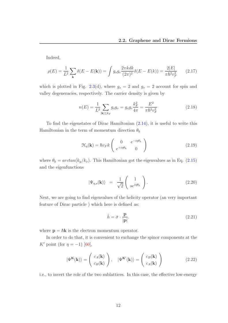
Figure 2.5: The contribution from intra and intervalley scattering (Fig. is takenfrom [3])
15
2.3. Electronic and Transport Properties in Disordered Graphene
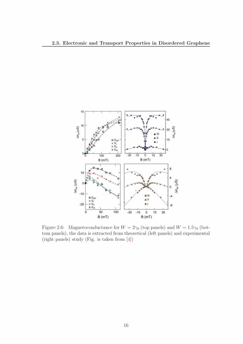
Figure 2.6: Magnetoconductance for W = 2γ0 (top panels) and W = 1.5γ0 (bot-tom panels), the data is extracted from theoretical (left panels) and experimental(right panels) study (Fig. is taken from [4])
16
2.3. Electronic and Transport Properties in Disordered Graphene
the weak antilocalization behavior but other effect should also be involved to
consider the whole picture, that is trigonal warping which is related to the mo-
mentum contribution from higher order into Eq. (2.15). The trigonal warping is
predicted to suppressed antilocalization and together with intervalley scattering,
it restores the weak localization (WL) [61]. The crossovers from WAL to WL
and the effect of disorders on intra- and intervalley scattering were studied in
many Refs. [61, 62, 3, 4] in which the long range disorder is simulated by chang-
ing onsite energies Vi =∑N
j=1 ǫj exp[−(ri − Rj)2/(2ξ2)] where ǫj are chosen at
random within[
−W2,−W
2
]
. These calculations show that the strength of local
potential profile control the contribution of intra- and intervalley scatterings on
the conductivity. Following the theoretical study in Ref. [3], the intravalley scat-
tering dominates at small value of W (W < γ0) and valley mixing strength was
continuously enhanced from W = γ0 to W = 2γ0. The intervalley scattering con-
tribution is large enough as W > 2γ0 (See. Fig. 2.5). As a consequence, graphene
exhibits the crossover from WAL to WL as W increase (See Fig. 2.6). Indeed,
the positive magnetoconductance for the case W = 2γ0 (top panels) agrees with
the strong contribution of intervalley scattering, since all graphene symmtries
have been broken. However by decreasing the disorder strength from W = 2γ0
to W = 1.5γ0 (bottom panels), WAL is indeed recovered given the reduction of
intervalley processes.
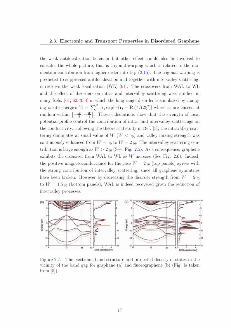
Figure 2.7: The electronic band structure and projected density of states in thevicinity of the band gap for graphane (a) and fluorographene (b) (Fig. is takenfrom [5])
17
2.3. Electronic and Transport Properties in Disordered Graphene
Chemical absorption in graphene is usually related to oxidation or hydro-
genation of graphene which are strongly invasive for electronic and transport
properties and systematically drive graphene to a strong Anderson insulator [64].
The theoretical and experimental studies show that high coverage sp3 formations
which break local AB symmetry such as in hydrogenated or fluorinated graphene
induce energy band gap in the high density limit. Especially, graphane, fully
hydrogenated graphene, is predicted to be a stable semiconductor with the en-
ergy gap as large as 3.5eV [65], some recent DFT calculations using the screened
hybrid functional of Heyd, Scuseria, and Ernzerhof (HSE) even gave a larger
energy gap up to 4.5eV for graphane and 5.1eV for fluorographene (fully fluo-
rinated graphene)(See Fig. 2.7). The case of low coverage of hydrogen is more
interesting with the transport properties strongly depending on the absorbing
position. Theory predicted that graphene exhibits WL for the compensated case
(hydrogen absorbs equally in two sublattices) whereas the quantum interferences
and localizations are suppressed if hydrogen defects are restricted to one of the
two sublattices [4]. The analogy of transport properties of chemical absorptions
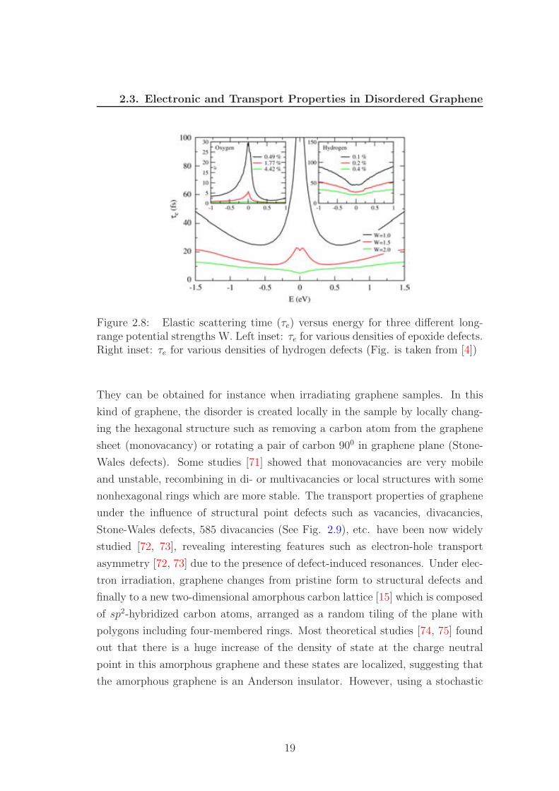
and long-range potentials have also been studied. As one can see in Fig. 2.8,
some chemical absorptions at bridge position such as epoxide defects which pre-
serve local AB symmetry induce energy-dependent elastic scattering time (τe(E))
ressembling the case of long range impurities with small onsite potential depth,
whereas some adsorbates at the top position such as hydrogen or fluorine de-
fects which break local sp2 and AB symmetry give rise to elastic scattering time
ressembling the case of strong long range potentials. These are due to the fact that
transport time behavior is controled by the contribution of inter- and intravalley
scatterings which are mainly determined by the breaking of AB symmetry.
In particular, the formation of sp3 hybridizations or monovacancies in graphene
can give rise to local sublattice imbalances and thus induce local magnetic mo-
ment according to Lie’s theorem [66] The existence of magnetism in graphene
as well as magnetism-dependent transport properties have been studied in many
Refs. [67, 68, 69]. Especially, when half of the hydrogen in graphane sheet is
removed, the resulting semihydrogenated graphene (graphone) becomes a ferro-
magnetic semiconductor with a small indirect gap [70].
Structural point defects usually exist in various geometrical forms in graphene.
18
2.3. Electronic and Transport Properties in Disordered Graphene
Figure 2.8: Elastic scattering time (τe) versus energy for three different long-range potential strengths W. Left inset: τe for various densities of epoxide defects.Right inset: τe for various densities of hydrogen defects (Fig. is taken from [4])
They can be obtained for instance when irradiating graphene samples. In this
kind of graphene, the disorder is created locally in the sample by locally chang-
ing the hexagonal structure such as removing a carbon atom from the graphene
sheet (monovacancy) or rotating a pair of carbon 900 in graphene plane (Stone-
Wales defects). Some studies [71] showed that monovacancies are very mobile
and unstable, recombining in di- or multivacancies or local structures with some
nonhexagonal rings which are more stable. The transport properties of graphene
under the influence of structural point defects such as vacancies, divacancies,
Stone-Wales defects, 585 divacancies (See Fig. 2.9), etc. have been now widely
studied [72, 73], revealing interesting features such as electron-hole transport
asymmetry [72, 73] due to the presence of defect-induced resonances. Under elec-
tron irradiation, graphene changes from pristine form to structural defects and
finally to a new two-dimensional amorphous carbon lattice [15] which is composed
of sp2-hybridized carbon atoms, arranged as a random tiling of the plane with
polygons including four-membered rings. Most theoretical studies [74, 75] found
out that there is a huge increase of the density of state at the charge neutral
point in this amorphous graphene and these states are localized, suggesting that
the amorphous graphene is an Anderson insulator. However, using a stochastic
19
2.3. Electronic and Transport Properties in Disordered Graphene
Figure 2.9: Some structural point defects (top panels) and their experimentalTEM images (bottom panels) (Fig. is taken from [6])
quenching method, Ref. [76] claimed that “we predict a transition to metallicity
when a sufficient amount of disorder is induced in graphene...”. In Chapter 4, by
using Kubo-Greenwood calculation, we show that this conclusion is misleading
and similar results have also been obtained recently in Ref. [77]
Although possessing many excellent electrical, optical and mechanical prop-
erties, perfect graphene (single-crystal graphene) is only fabricated in small size
by exfoliation method. So far, the most promising approach for the mass produc-
tion of large-area graphene is chemical vapor deposition (CVD), which results in
a graphene with many line defects (See Fig. 2.10) or polycrystalline graphene.
This polycrystallinity arises due to the nucleation of growth sites at random po-
sitions and orientations during the CVD process. In order to accommodate the
lattice mismatch between misoriented grains, the grain boundaries in polycrys-
talline graphene are made up of a variety of non-hexagonal carbon rings, which
can act as a source of scattering during charge transport. Because of its poten-
tial for applications, the transport properties of polycrystalline graphene are the
subject of intense research. Some calculations showed that the effect of grain
boundaries on the carrier transport differ depending on the grain-boundary ge-
ometry (See Fig. 2.10) resulting in a tunable mobility (tunable transport gaps)
[7] which allows to control charge currents without the need to introduce bulk
band gaps in graphene. In so-called class I grain boundaries (top panels of Fig.
20
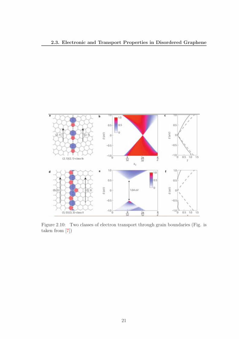
2.3. Electronic and Transport Properties in Disordered Graphene
Figure 2.10: Two classes of electron transport through grain boundaries (Fig. istaken from [7])
21
2.4. Spin Transport in Graphene
2.10), including all symmetrical grain boundaries, the projected periodicities of
the lattice on each side match in a way that allows carriers to cross freely even
at the Dirac point. In class II grain boundaries (bottom panels of Fig. 2.10),
no such momentum-conserving transmission is possible, except for carriers with
much higher energy. Another calculation pointed out that some line defects can
play the role as semitransparent “valley filter”. It was found that carriers arriving
at this line defect with a high angle of incidence are transmitted with a valley po-
larization near 100% [78]. Many experimental works have studied the transport
properties of polycrystalline graphene and showed that the grain boundaries gen-
erally degrade the electrical performance of graphene [26, 14] and specially, the
interdomain connectivity play an important role to control the electrical proper-
ties of polycrystalline graphene, with the electrical conductance that can improve
by one order of magnitude for grain boundaries with better interdomain con-
nectivity [26]. However, just a few theoretical works have studied the complex
structures of grain boundaries and corresponding electronic transport. In Chap-
ter 4, by using the molecular dynamics, we simulate the polycrystalline graphene
with variable grain sizes, and tunable interdomain connectivities, and report on a
scaling law for transport properties of polycrystalline graphene, which points out
that the semiclassical conductivity and mean free path are directly proportional
to grain size and both are strongly affected by grain connectivity. However,
as pointed out in our next calculation, the grain boundary resistivity for non-
contaminated polycrystalline graphene is very low compared to the experimental
results [25, 26, 79]. The explanation for this problem is that the grain boundaries
which contain many nonhexagonal structure have greater chemical reactivity [80]
and are usually functionalized by many different types of chemical adsorbates.
This has been confirmed in several experiments [28, 18]. By using the numer-
ical simulations we report on the role played by chemical adsorbates on grain
boundaries in charge transport in Chapter 4
2.4 Spin Transport in Graphene
Beside many interesting electronic properties, graphene is also considered to be
a promising candidate for spintronic applications. The spin relaxation time in
22
2.4. Spin Transport in Graphene
intrinsic graphene is expected to be very long and therefore graphene has high
potential as a spin-conserver system which can transmit spin-encoded information
across a device with high fidelity. The underlying reason for long spin relaxation
time is the low hyperfine interactions of the spin with the carbon nuclei (natural
carbon only contains 1% 13C) and the weak spin-orbit coupling (SOC) due to
the low atomic number [81]. The theoretical prediction showed that the spin
relaxation time in graphene is in the order of microseconds. However, the reported
experimental spin relaxation times remain several orders of magnitude lower than
the original theoretical predictions.
Because spin relaxation based on the graphene intrinsic SOC could not give a
convincing explanation, other extrinsic sources of spin relaxation are believed to
come into play. Proposals to explain the unexpectedly short spin relaxation times
include spin decoherence due to interactions with the substrate, the extrinsic
SOC induced by impurities, adatoms, ripples or corrugations, etc. which will be
reviewed below. The puzzling controversy of spin relaxation mechanism will be
mentioned in the next section.
2.4.1 Spin-Orbit Coupling in Graphene
In order to derive the spin orbit coupling term in the Hamiltonian, it is necessary
to start from the relativistic Hamiltonian, the Dirac equation: H|ψ〉 = E|ψ〉 with
H =
(
0 cp.σ
cp.σ 0
)
+
(
mc2 0
0 −mc2
)
+ V (2.26)
and the wave function is two-components spinor: |ψ〉 = (ψA, ψB)T . From the
Dirac equation we obtain two equations for spinor components:
ψB =cp.σ
E − V +mc2ψA (2.27)
p.σc2
E − V +mc2p.σψA = (E − V −mc2)ψA (2.28)
In the nonrelativistic limit, the lower components ψB is very small compared to
the upper component ψA. Indeed, with the relativistic energy E = mc2 + ǫ and
23
2.4. Spin Transport in Graphene
V ≪ mc2, Eq. (2.27) drive us to
ψB =p.σ
2mcψA ≪ ψA (2.29)
and Eq. (2.28) leads to the Schrodinger equation.1
(
p2
2m+ V
)
ψA = ǫψA (2.30)
In other words, in the first order of (v/c), ψA is equivalent to the Schrodinger
wave function ψ. In order to obtain the analogy of ψA and ψ at higher order of
(v/c), we use the normalization characteristic of the wave function
∫
(
ψ+AψA + ψ+
BψB
)
= 1 (2.31)
To first order, using Eq. (2.29), this gives
∫
ψ+A
(
1 +p2
4m2c2
)
ψA = 1 (2.32)
Apparently, to have a normalized wave function, we should use ψ =(
1 + p2
8m2c2
)
ψA.
Substituting this into the Dirac equation, and using the expansion c2
E−V+mc2≃
12m
(
1 − ǫ−V2mc2
+ ...)
, we obtain, after some rearrangement, the Pauli equation
(
p2
2m+ V − p4
8m3c2− ~
4m2c2σ.p×∇V +
~2
8m2c2∇2V
)
ψ = ǫψ (2.33)
the first and the second terms are the usual terms in the Hamiltonian, the third
term is simply a relativistic correction to the kinetic energy. The fourth term is
the spin-orbit coupling term and the final term give the energy shift due to the
potential.
Hereafter, I will derive the spin-orbit coupling term in the more intuitive way
which gives the physical meaning of SOC interation. Suppose an electron is
moving with velocity v in an electric field −eE = −∇V . This electric field might
be induced by the potential V of the adatoms or the substrate. In relativistic
1using (σ.A)(σ.B) = A.B+ iσ.(A×B)
24
2.4. Spin Transport in Graphene
theory, this moving electron feels a magnetic field B = −v×Ec
in its rest frame.
The interation between this magnetic field and the electron spin leads to the
potential energy term:
Vµs= −µsB = −gsµB
2ecσ.v ×∇V = − gs~
4m2c2σ.p×∇V = − ~
2m2c2σ.p×∇V
(2.34)
This results is twice the SOC term in Pauli equations. Actually, this was the ma-
jor puzzle, until it was pointed out by Thomas [82] that this argument overlooks
a second relativistic effect that is less widely known, but is of the same order
of magnitude: electric field E causes an additional acceleration of the electron
perpendicular to its instantaneous velocity v, leading to a curved electron trajec-
tory. In essence, the electron moves in a rotating frame of reference, implying an
additional precession of the electron, called the Thomas precession. As a result,
electron “sees” that the magnetic field has only one-half the above value
B = −v × E
2c(2.35)
which leads to the full SOC term
VSOC = − ~
4m2c2σ.p×∇V (2.36)
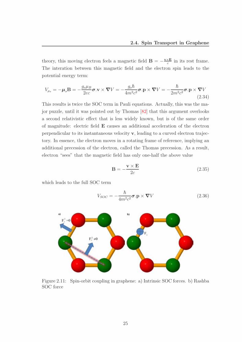
Figure 2.11: Spin-orbit coupling in graphene: a) Intrinsic SOC forces. b) RashbaSOC force
25
2.4. Spin Transport in Graphene
Now let’s rewrite the SOC term in form of SOC force F
HSOC = α (F× p) .s = −α (s× p) .F (2.37)
where α is an undetermined parameter. Here we use s instead of σ to represent
the spin degree of freedom to avoid any misunderstanding with pseudospin in
graphene.
If we consider the intrinsic graphene, the inversion symmetry dictates the
electric field (force) in plane and this SOC is called intrinsic SOC. Because of
structure’s mirror symmetry with respective to any nearest-neighbor bond (See
Fig. 2.11(a)), the nearest-neighbor intrinsic SOC is zero, while the next nearest-
neighbor intrinsic SOC is nonzero. According to symmetry,
HI = iγ2
(
F// × dij
)
.s =2i√
3VIs.(dkj × dik) (2.38)
where γ2 and VI are undetermined parameters, and dij is the unit vector from
atom j two its next-nearest neighbors i, and k is the common nearest neighbor
of i and j
In the presence of the out of plane electric field (See Fig. 2.11(b)) which can
originate from a gate voltage or charged impurities in the substrate, adatoms,
etc., the band structure of graphene changes. This external electric field breaks
spatial inversion symmetry and causes a nearest-neighbor extrinsic SOC. This
SOC is Rashba SOC and has the form
HR = iγ1
(
s× dij
)
.F⊥ez = iVRz.(s× dij) (2.39)
where j is the nearest-neighbor of i and γ1 and VR are undetermined parameters.
Finally, we get the tight-binding Hamiltonian:
H = −γ0∑
〈ij〉
c+i cj +2i√
3VI∑
〈〈ij〉〉
c+i s.(dkj × dik)cj + iVR∑
〈ij〉
c+i z.(s× dij)cj (2.40)
By performing Fourier transformations, we obtain the low energy effective
26
2.4. Spin Transport in Graphene
Hamitoniam around the Dirac point in the basis |A〉, |B〉 ⊗ | ↑〉, | ↓〉
h(k) = h0(k) + hR(k) + hI(k) (2.41)
where
h0(k) = ~vF (ησxkx + σyky) ⊗ 1s
hR(k) = λR (η [σx ⊗ sy] − [σy ⊗ sx])
hI(k) = λIη [σz ⊗ sz] (2.42)
with Fermi velocity vF = 32γ0, Rashba spin-orbit coupling λR = 3
2VR and intrinsic
spin-orbit coupling λI = 3√
3VI [83]
The remarkable thing about SOC in graphene is that the SOC terms are
momentum-independent. The spin directly couples with pseudospin instead of
momentum as in conventional metals or semiconductors, the usual SOC term
(k× s) is small and can be disregarded.
Diagonalizing the Hamiltonian in Eq. (2.41) give the electronic bands at close
to the Dirac point [8, 84]:
ǫµν(k) = µλR + ν√
(~vFk)2 + (λR − λI)2 (2.43)
where µ and ν = ±1 are band indexes.
If we consider intrinsic graphene the Rashba SOC is vanishingly small, the
intrinsic SOC opens a gap ∆ = 2λI (See Fig. 2.12(a)). When Rashba SOC is
turned on by inversion symmetry breaking (effect from the substrate, the electric
field, the corrugations, etc.), the competition of Rashba and intrinsic SOC leads
to gap closing. The gap remains finite ∆ = 2(λI − λR) for 0 < λR < λI (Fig.
2.12(b)). For λR > λI the gap closes and the electronic structure is that of a zero
gap semiconductor with quadradically dispersing bands (Fig. 2.12(d)).
The eigenfunctions correspond to the eigenvalues in Eq. (2.43) are
ψµν(k) =
(
χ−|ηe−iηϕ
[
ǫµν − λIν~vF k
]η
, 1〉 + µχ+|−iηe−i(1+η)ϕ, ie−iϕ
[
λI − ǫµνν~vFk
]η
〉)
/Cµν
27
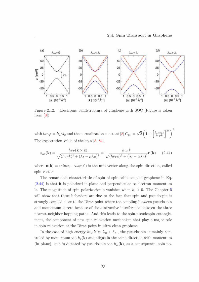
2.4. Spin Transport in Graphene
Figure 2.12: Electronic bandstructure of graphene with SOC (Figure is takenfrom [8])
with tanϕ = ky/kx and the normalization constant [8] Cµν =√
2
(
1 +[
λI−ǫµν~vF k
]2η)2
The expectation value of the spin [8, 84],
sµν(k) =~vF (k× z)
√
(~vFk)2 + (λI − µλR)2=
~vFk√
(~vFk)2 + (λI − µλR)2n(k) (2.44)
where n(k) = (sinϕ,−cosϕ, 0) is the unit vector along the spin direction, called
spin vector.
The remarkable characteristic of spin of spin-orbit coupled graphene in Eq.
(2.44) is that it is polarized in-plane and perpendicular to electron momentum
k. The magnitude of spin polarization s vanishes when k → 0. The Chapter 5
will show that these behaviors are due to the fact that spin and pseudospin is
strongly coupled close to the Dirac point where the coupling between pseudospin
and momentum is zero because of the destructive interference between the three
nearest-neighbor hopping paths. And this leads to the spin-pseudospin entangle-
ment, the component of new spin relaxation mechanism that play a major role
in spin relaxation at the Dirac point in ultra clean graphene.
In the case of high energy ~vFk ≫ λR + λI , the pseudospin is mainly con-
troled by momentum via h0(k) and aligns in the same direction with momentum
(in plane), spin is dictated by pseudospin via hR(k), as a consequence, spin po-
28
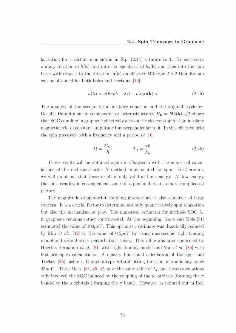
2.4. Spin Transport in Graphene
larization for a certain momentum in Eq. (2.44) saturate to 1. By successive
unitary rotation of h(k) first into the eigenbasis of h0(k) and then into the spin
basis with respect to the direction n(k) an effective BR-type 2 × 2 Hamiltonian
can be obtained for both holes and electrons [10],
h(k) = ν(~vFk − λI) − νλRn(k).s (2.45)
The analogy of the second term in above equation and the original Bychkov-
Rashba Hamiltonian in semiconductor heterostructures Hk = ~Ω(k).s/2 shows
that SOC coupling in graphene effectively acts on the electrons spin as an in-plane
magnetic field of constant amplitude but perpendicular to k. In this effective field
the spin precesses with a frequency and a period of [10]
Ω =2λR~, TΩ =
π~
λR(2.46)
These results will be obtained again in Chapter 5 with the numerical calcu-
lations of the real-space order N method implemented for spin. Furthermore,
we will point out that these result is only valid at high energy. At low energy
the spin-pseudospin entanglement comes into play and creats a more complicated
picture.
The magnitude of spin-orbit coupling interactions is also a matter of large
concern. It is a crucial factor to determine not only quantitatively spin relaxation
but also the mechanism at play. The numerical estimates for intrinsic SOC λI
in graphene remains rather controversial. At the beginning, Kane and Mele [51]
estimated the value of 100µeV . This optimistic estimate was drastically reduced
by Min et al. [42] to the value of 0.5µeV by using microscopic tight-binding
model and second-order perturbation theory. This value was later confirmed by
Huertas-Hernando et al. [81] with tight-binding model and Yao et al. [85] with
first-principles calculations. A density functional calculation of Boettger and
Trickey [86], using a Gaussian-type orbital fitting function methodology, gave
25µeV . Three Refs. [81, 85, 42] gave the same value of λI , but these calculations
only involved the SOC induced by the coupling of the pz orbitals (forming the π
bands) to the s orbitals ( forming the σ band). However, as pointed out in Ref.
29
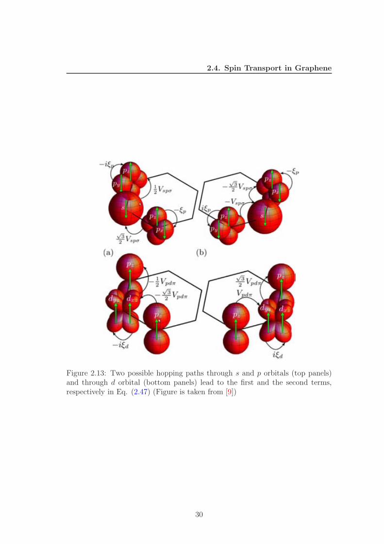
2.4. Spin Transport in Graphene
Figure 2.13: Two possible hopping paths through s and p orbitals (top panels)and through d orbital (bottom panels) lead to the first and the second terms,respectively in Eq. (2.47) (Figure is taken from [9])
30
2.4. Spin Transport in Graphene
[9] that the coupling of the pz orbitals to the d orbitals (See Fig. 2.13) dominates
the SOC at K(K ′). Due to a finite overlap between the neighboring pz and dxz,
dyz orbitals, the intrinsic splitting λI is linearly proportional to the spin-orbit
splitting of the d states, ξd (orbitals higher than d have a smaller overlap and
contribute less). In contrast, due to the absence of the direct overlap between
the pz and σ-band orbitals, the usually considered spin-orbit splitting [81, 85, 42]
induced by the σ−π mixing depends only quadratically on the spin-orbit splitting
of the pz orbital, ξp, giving a negligible contribution.
λI ≃2(εp − εs)
9V 2spσ
ξ2p +9V 2
pdπ
2(εd − εp)2ξd (2.47)
where εs,p,d are the energies of s, p, d orbitals, respectively and Vspσ and Vpdπ are
hopping parameters of the p orbital to the s and d orbital, respectively.
Figure 2.14: A representative hopping path is responsible for Rashba SOC inEq. (2.48) (Figure is taken from [9])
This tight-binding calculation gave the value of intrinsic SOC λI = 12µeV [9]
and was confirmed by the first principle calculation [8]. These calculations also
showed that the Rashba term (zero in absence of electric field) is tunable with an
31
2.4. Spin Transport in Graphene
external electric field E which is perpendicular to graphene plane
λR ≃ 2eEzsp3Vspσ
ξp +√
3eEzsp
(εd − εp)
3Vpdπ(εd − εp)
ξd (2.48)
where zsp and zpd are the expectation values 〈s|z|pz〉 and 〈pz|z|dz2〉, respectively,
of the operator z.
All these calculations predicted that the Rashba SOC is directly proportional
to the electric field E but the estimated values vary by about an order of mag-
nitude from 5µeV in Ref. [8] to 47µeV in Ref. [81] and to 67µeV in Ref. [42],
for a typical electric field of E = 1V/nm. Furthermore, C. R. Ast and I. Gierz
[87] used the tight-binding model and directly considered the nearest-neighbor
contribution from the electric field and obtained λR = 37.4µeV .
In general, the intrinsic SOC of graphene is very weak, in the order of µeV
and is unmeasurable. This makes some phenomena such as Quantum Spin Hall
(QSH) effect unobservable in graphene the material in which it was originally
predicted [51]. A way to observe QSH effect in graphene is endowing it with
heavy adatoms which increase SOC in graphene, this problem will be mentioned
in Chapter 5.
2.4.2 Spin Transport in Graphene
The graphene SOC in the order of µeV as mentioned above should lead to spin
relaxation times in the microsecond scale [10]. However, the experimental results
is in the order of nanoseconds, several orders of magnitude lower than the original
theoretical prediction. In order to clarify the limitations and mechanisms for spin
relaxation in graphene a lot of effort has been done by both experimentalists and
theoreticians, but up to now this topic is still under debate. The first measure-
ment of electron spin relaxation was performed by N. Tombros et. al. [44] using
the non-local spin valve measurement and Hanle spin precession method to study
spin relaxation in mechanical exfoliated single-layer graphene (SLG) on SiO2 sub-
strate with mobility of the devices about 2, 000cm2V −1s−1. They extracted the
spin relaxation time of few hundreds of ps and spin relaxation length of few µm at
room temperature, similar to what one might expect for conventional metals or
semiconductors, this value has been confirmed by several measurements [58, 46].
32
2.4. Spin Transport in Graphene
The spin transport was found to be relatively insensitive to the temperature and
weakly dependent on the direction of spin injection and charge density. Due to the
fast spin relaxation was attributed to the extrinsic SOC in the substrate and the
way to grow graphene, spin measurements in many other kinds of graphene and
substrates have been reported. The measurement of spin relaxation on epitaxially
grown graphene on SiC(0001) [88] is the first report of spin transport in graphene
on a different substrate than SiO2. The value of spin relaxation τs was obtained
in the order of few nanoseconds, one order of magnitude larger than in exfoliated
graphene on SiO2. However the spin diffusion coefficient Ds ≈ 4cm2/s is about
80 times smaller, yielding to 70% lower value for spin relaxation length λs. The
longer τs but much smaller Ds was later explained by the influence of localized
states arising from the buffer layer at the interface between the graphene and the
SiC surface that couple to the spin transport channel [89]. The measurement
also reported that τs is weakly influenced by the temperature with reductions
of Ds by more than 40% and τs by about 20% at room temperature. With the
expectation that removing the underneath substrate helps to reduce the extrinsic
SOC and leads to long spin relaxation time, the spin measurement on suspended
graphene was performed [90]. Although a high mobility µ ≈ 105cm2V −1s−1 , an
increase up to an order of magnitude in spin diffusion coefficient (Ds = 0.1m2/s)
compared to SiO2 supported graphene and long mean free path in the order of
a µm were observed, indicate that much less scattering happens, the spin re-
laxation time remains a few hundreds of ps and spin relaxation length few µm.
Other group used chemical vapor deposition (CVD) method to grow graphene
on cooper (Cu) substrate and studied the effect of corrugation on spin relaxation
time [45]. They observed the same spin relaxation time as in exfoliated graphene
and showed that ripples in graphene flakes have minor effects on spin transport
parameters.
The nature of spin relaxation is actually a fundamental debated issue. The
D’yakonov-Perel (DP) [91, 92, 53] and the Elliot-Yafet (EY) [93, 11] are two
mechanisms usually discussed in the context of graphene. The EY mechanism is a
suitable mechanism for spin relaxation in metals. In the EY mechanism, electron
spin changes its direction during the scattering event thanks to the SOC which
produces admixtures of spin and electron momentum in the wave functions. Due
33
2.4. Spin Transport in Graphene
to these admixtures, scattering changes electron momentum and induces spin-flip
probability at the same time and leads to a typical scaling behavior of spin re-
laxation time with momentum relaxation time τEYs ∼ τp. On the other hand, DP
mechanism is an efficient mechanism for materials with broken inversion sym-
metry. In these kinds of materials, SOC induces effective momentum-dependent
magnetic field about which electron spin precesses between scattering events.
The longer time electron travels, the larger angle electron spin precesses and as
a consequence, the more spin dephasing between electrons in the ensemble is ac-
cumulated. Therefore, spin relaxation time is inversely proportional to elastic
scattering time τDPs ∼ τ−1
p . W. Han and R. K. Kawakami performed system-
atic studies of spin relaxation in SLG and bilayer graphene (BLG) spin valves
with tunneling contact [46]. They found that in SLG, the spin relaxation time
varies linearly with momentum scattering time τp, indicating the dominance of
EY spin relaxation whereas in BLG, τs and τp exhibit an inverse dependence,
which indicates the dominance of DP mechanism. However, Pi et. al. reported a
surprising result that τs increases with decreasing τp in the surface chemical dop-
ing experiment with Au atoms on graphene [56], indicating that the DP mech-
anism is important there. This experiment led to the conclusion that charged
impurity scattering is not the dominant mechanism for spin relaxation, despite
its importance for momentum scattering. Even more puzzling, P. J. Zomer et.
al. performed spin transport measurements on graphene deposited on boron ni-
tride with mobilities up to 4.104cm2V −1s−1 and showed that neither EY nor DP
mechanisms alone allow for a fully consistent description of spin relaxation [47].
Furthermore, electron spin is expected to relaxe faster in BLG than in SLG be-
cause the SOC in BLG is one order of magnitude larger than the one in SLG due
to the mixing of π and σ bands by interlayer hopping [94], but the experimental
results showed an opposite behavior [46, 95]. The spin relaxation time in BLG
has been reported in the order of few nanoseconds and show the dominance of
DP spin scattering [46, 95].
D’yakonov-Perel mechanism:
As one can see from Eq. (2.45), electron precesses about the effective mag-
netic field in plane B‖(k) ∼ Ω(k) between scattering events. Random scattering
induces motional narrowing of this spin precession causing spin relaxation (See
34
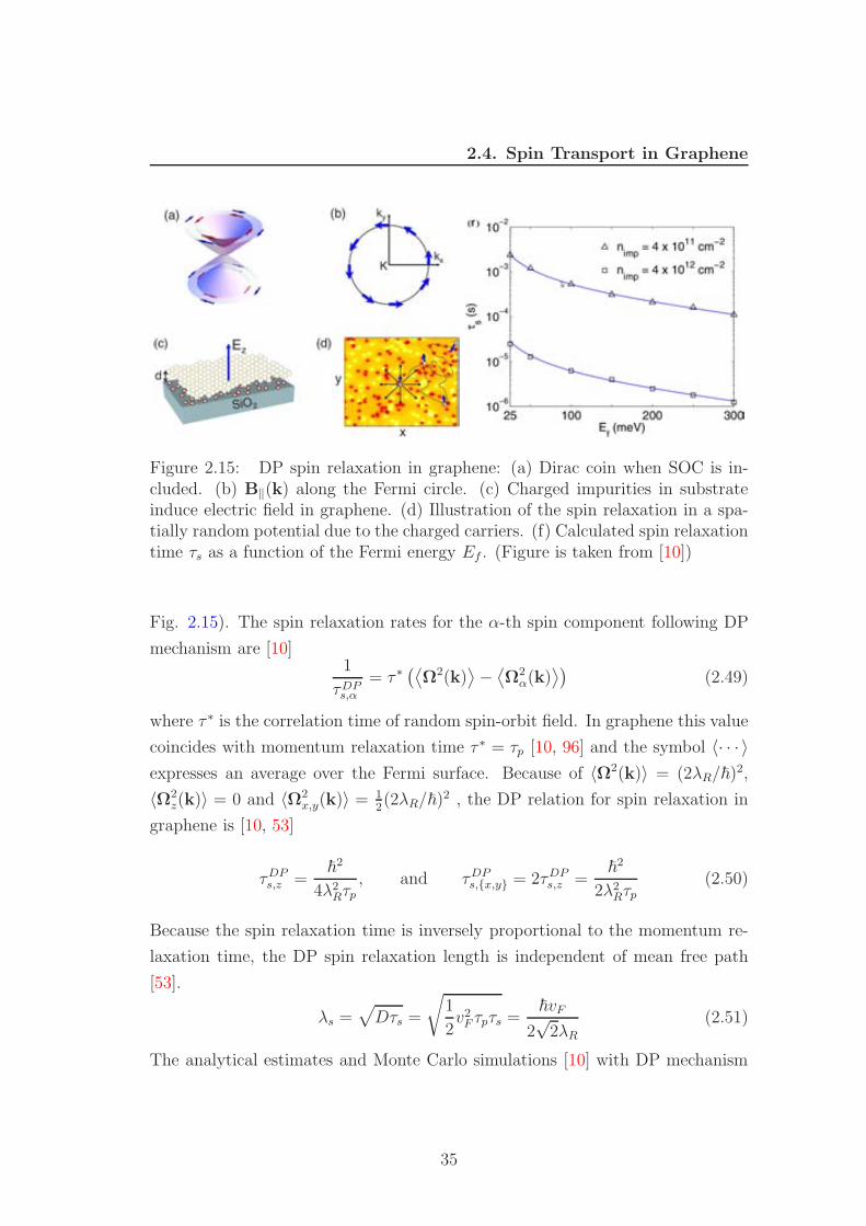
2.4. Spin Transport in Graphene
Figure 2.15: DP spin relaxation in graphene: (a) Dirac coin when SOC is in-cluded. (b) B‖(k) along the Fermi circle. (c) Charged impurities in substrateinduce electric field in graphene. (d) Illustration of the spin relaxation in a spa-tially random potential due to the charged carriers. (f) Calculated spin relaxationtime τs as a function of the Fermi energy Ef . (Figure is taken from [10])
Fig. 2.15). The spin relaxation rates for the α-th spin component following DP
mechanism are [10]1
τDPs,α
= τ ∗(⟨
Ω2(k)⟩
−⟨
Ω2α(k)
⟩)
(2.49)
where τ ∗ is the correlation time of random spin-orbit field. In graphene this value
coincides with momentum relaxation time τ ∗ = τp [10, 96] and the symbol 〈· · · 〉expresses an average over the Fermi surface. Because of 〈Ω2(k)〉 = (2λR/~)2,
〈Ω2z(k)〉 = 0 and 〈Ω2
x,y(k)〉 = 12(2λR/~)2 , the DP relation for spin relaxation in
graphene is [10, 53]
τDPs,z =
~2
4λ2Rτp, and τDP
s,x,y = 2τDPs,z =
~2
2λ2Rτp(2.50)
Because the spin relaxation time is inversely proportional to the momentum re-
laxation time, the DP spin relaxation length is independent of mean free path
[53].
λs =√
Dτs =
√
1
2v2F τpτs =
~vF
2√
2λR(2.51)
The analytical estimates and Monte Carlo simulations [10] with DP mechanism
35
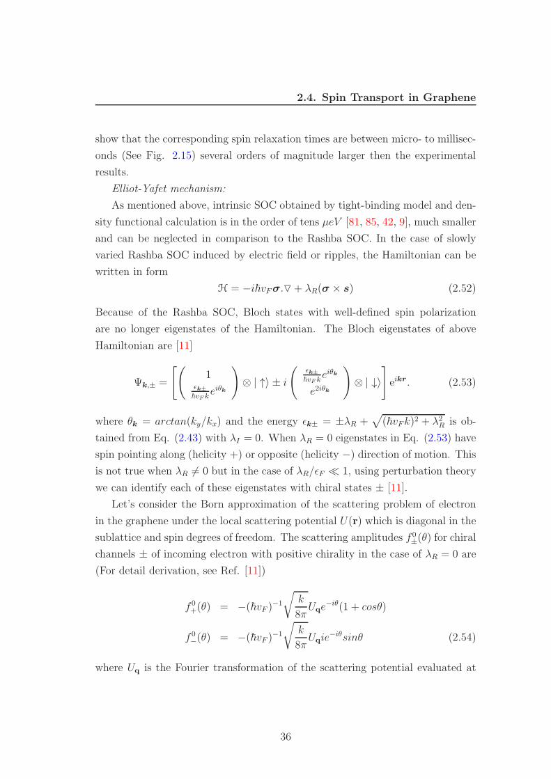
2.4. Spin Transport in Graphene
show that the corresponding spin relaxation times are between micro- to millisec-
onds (See Fig. 2.15) several orders of magnitude larger then the experimental
results.
Elliot-Yafet mechanism:
As mentioned above, intrinsic SOC obtained by tight-binding model and den-
sity functional calculation is in the order of tens µeV [81, 85, 42, 9], much smaller
and can be neglected in comparison to the Rashba SOC. In the case of slowly
varied Rashba SOC induced by electric field or ripples, the Hamiltonian can be
written in form
H = −i~vFσ. + λR(σ × s) (2.52)
Because of the Rashba SOC, Bloch states with well-defined spin polarization
are no longer eigenstates of the Hamiltonian. The Bloch eigenstates of above
Hamiltonian are [11]
Ψk,± =
[(
1ǫk±~vF k
eiθk
)
⊗ | ↑〉 ± i
(
ǫk±~vF k
eiθk
e2iθk
)
⊗ | ↓〉]
eikr. (2.53)
where θk = arctan(ky/kx) and the energy ǫk± = ±λR +√
(~vFk)2 + λ2R is ob-
tained from Eq. (2.43) with λI = 0. When λR = 0 eigenstates in Eq. (2.53) have
spin pointing along (helicity +) or opposite (helicity −) direction of motion. This
is not true when λR 6= 0 but in the case of λR/ǫF ≪ 1, using perturbation theory
we can identify each of these eigenstates with chiral states ± [11].
Let’s consider the Born approximation of the scattering problem of electron
in the graphene under the local scattering potential U(r) which is diagonal in the
sublattice and spin degrees of freedom. The scattering amplitudes f 0±(θ) for chiral
channels ± of incoming electron with positive chirality in the case of λR = 0 are
(For detail derivation, see Ref. [11])
f 0+(θ) = −(~vF )−1
√
k
8πUqe
−iθ(1 + cosθ)
f 0−(θ) = −(~vF )−1
√
k
8πUqie
−iθsinθ (2.54)
where Uq is the Fourier transformation of the scattering potential evaluated at
36
2.4. Spin Transport in Graphene
Figure 2.16: Sketch of scattering by a potential U(r) in the chiral channels(Figure is taken from [11])
the transferred momentum q = k′ − k and angle θ (see Fig. 2.16) between the
outgoing momentum k′ and incoming momentum k.
When Rashba SOC is turned on these amplitudes become
fλR+ (θ) = −(~vF )−2
√
1
8πk+(ǫ + (ǫ− 2λR)cosθ)Uq+e
−iθ
fλR− (θ) = −(~vF )−2
√
1
8πk−(ǫ + 2λR)Uq−
ie−iθsinθ (2.55)
where k± = (~vF )−1√ǫ2 ∓ 2ǫλR and q± = k′
± − k
Let us define the probability for a spin-flip process from the changes in the
scattering in both chiral channels due to the presence of the SO coupling.
S(θ) =
∑
±1 |f 0±(θ)||fλR
± (θ) − f 0±(θ)|
∑
±1 |f 0±(θ)|2 (2.56)
This is the amount of spin relaxed in the direction defined by θ. The total amount
of spin relaxation during a scattering event can be defined as the average of this
37
2.4. Spin Transport in Graphene
quantity over the Fermi surface:
S = 〈S(θ)〉 =1
2π
∫
dθS(θ, ǫ = ǫF ) (2.57)
It is easy to see that fλR± (θ) − f 0
±(θ) ∼ λR/ǫF from expanding of Eq. (2.55)
in powers of λR/ǫF . This implies that S(θ) ∼ λR/ǫF which is independent on
the scattering potentials U(r). This result was obtained in Ref. [53] for the
case of weak scatterers, and later in Ref. [11] for the cases of scattering by
boundary, strong scatterers and clusters of impurities which can not be treated
in perturbation theory. Assuming this behavior, the EY relation for graphene
can be easily found. Indeed, the change of spin orientation at each collision is
S ∼ λR/ǫF . The total change of spin orientation after Ncol collisions is of the
order of√NcolǫF/λR. Dephasing occurs when
√NcolǫF/λR ∼ 1 and of course,
after a time τEYs = Ncolτp. Hence we obtain the EY relation
τEYs ≈ ǫ2F
λ2Rτp (2.58)
This is the Elliot-Yafet relation for graphene. It is worth to mention that the
spin relaxation time τs here not only is proportional to momentum relaxation
time τp but also depends on the carrier density through Fermi energy ǫF . The
spin relaxation length in EY mechanism is proportional to mean free path ℓe
λs =√
Dτs =
√
1
2v2F τpτs ∼ ℓe
ǫF√2λR
(2.59)
Despite the fact that some experiments have reported that τs ∼ τp, indicating
the dominance of EY mechanism in spin relaxation in graphene, the discrepancy
between theoretical calculations and experimental data is still large. Furthermore,
the derivations of both EY and DP for graphene are based on the strong coupling
of momentum and pseudospin which is unsuitable close to the Dirac point. In
Chapter 5, we propose a new mechanism which is the heart of this PhD thesis
to explains the fast spin relaxation in graphene by the entanglement of spin and
pseudospin degrees of freedom.
38
Chapter 3
The Real Space Order O(N )
Transport Formalism
Quantum simulations are very important tools to study transport phenomena
in the nanoscale. There are two numerical approaches for quantum transport
simulations at the present, one is the widely used non-equilibrium Green’s func-
tion (NEGF) method, the other is the Kubo-Greenwood method. While NEGF is
usually used for small systems such as carbon nanotubes (CNT), graphene nanori-
bons (GNRs), due to the cubic-scaling time consumption, the linear-scaling Kubo-
Greenwood quantum transport simulation method is a very effective method to
investigate the transport properties of the large-scale disoder systems.
In this chapter, the theoretical background of Kubo-Greenwood formalism, the
real-space Kubo formulas for conductivity and the Einstein relations are derived
in the first section. At the end of this section the three different regimes of
transport is discussed. In the second section, a new formalism basing on the real
space order O(N) is firstly developed to study the spin transport in large scale
2D system. This method is applied in Chapter 5 to study the spin transport in
disordered graphene.
39
3.1. Electric Transport Formalism
3.1 Electrical Transport Formalism
3.1.1 Electrical Resistivity and Conductivity
When there is a electric field E(ω) inside a material, it will cause electric current to
flow. Electrical resistivity ρ(ω) is a measure of how strongly a material opposes
the flow of electric current. A low resistivity indicates a material that readily
allows the movement of electric charge. The electrical resistivity is defined as the
ratio of the electric field to the density of the current j(ω) it creates
j(ω) =E(ω)
ρ(ω)(3.1)
Conductivity σ(ω) is the inverse of resistivity
σ(ω) =1
ρ(ω)(3.2)
Therefore, we have
j(ω) = σ(ω)E(ω) (3.3)
We usually measure the response of system to the electric field along 1 direction
(ex. the x direction). In this case, the conductivity σ (more detail σxx) on this
direction is:
jx(ω) = σ(ω)Ex(ω) (3.4)
σ(ω) is the conductivity in the general case. For the direct current (DC), the DC
conductivity σDC can be obtain by setting ω → 0
3.1.2 Semiclassical Approach
Firstly, let’s use the semiclassical approach to have the general picture of the mo-
tion of electron in the system under the influence of electric field. In this section
some formulas such as Drude conductivity, Einstein relation, and Landauer for-
mula are derived which will give a better vision for the quantum approach which
will be given in the next section.
In the presence of an electric field E in the plane of the two dimensional
40
3.1. Electric Transport Formalism
electron gas (2DEG) system, beside thermal motion, electron moves along the
direction of electric force. However, this drift motion only remains in a short
time before its direction is randomized by scattering on disorder. An electron
acquires a drift velocity vdrift = −eE∆t/m in the time ∆t since the last impurity
collision. The average of ∆t is the scattering time τp (or momentum relaxation
time), so the average drift velocity vdrift is given by [12]
vdrift = −µeE, µe =eτpm
(3.5)
where µe is electron mobility. If the sheet density is ns then the current density
is
j = −ensvdrift = σE (3.6)
The result is the familiar Drude conductivity [97] which can be written in several
equivalent forms:
σ = ensµe =ensτpm
= gsgve2
h
kF l
2(3.7)
In the last equality we have used the identity ns = gsgvk2F/4π which is true for
all 2DEG system including graphene [2] and have defined the mean free path
ℓe = vF τp. The valley degeneracy factors are typically gv = 2 for graphene (K
and K ′) and Si 100 based 2DEG system, whereas gv = 1(6) for 2DEG system in
GaAs (Si 111). The spin degeneracy is always gs = 2, except at high magnetic
fields.
It is obvious that the current induced by the applied electric field is carried
by all conduction electrons, since each electron acquires the same average drift
velocity. Nonetheless, to determine the conductivity it is sufficient to consider
the response of electrons near the Fermi level to the electric field. The reason is
that the states that are more than a few times the thermal energy kBT below EF
are all filled so that in response to a weak electric field only the distribution of
electrons among states at energies close to EF is changed from the equilibrium
Fermi-Dirac distribution
f(E − EF ) =
(
1 + eE−EFkBT
)−1
(3.8)
41
3.1. Electric Transport Formalism
In thermodynamic equilibrium at zero temperature which is characterized
by a spatially constant electrochemical potential µ, the sum of the drift current
density −σE/e and the diffusion current density −D∇ns (D is diffusion constant)
vanishes
−σE/e−D∇ns = 0 when ∇µ = 0 (3.9)
The electrochemical potential µ is the sum of the electrostatic potential energy
−eV and the chemical potential at EF . Since dEF/dns = 1/ρ(EF ), one has
∇µ = −e∇V + ∇EF = eE +∇ns
ρ(EF )(3.10)
The combination of Eqs. (3.9) and (3.10) yields the Einstein relation for the
conductivity σ
σ = e2ρ(EF )D (3.11)
To verify that Eq. (3.11) is consistent with the earlier expression (3.7) for the
Drude conductivity, one can use the result (see below) for the 2D diffusion con-
stant:
D =1
2v2F τp =
1
2vF l (3.12)
in combination with the density of states: ρ(E) = gsgvE/2π(~vF )2 for graphene
and ρ(E) = gsgvm/2π~2 for 2DEG systems
The result in Eq. (3.12) can be explained in the following way [12]. Consider
the diffusion current density jx induced by a small constant density gradient,
n(x) = n0 + cx. We write
jx = lim∆t→∞
〈vx(t = 0)n(x(t = −∆t))〉= lim
∆t→∞c 〈vx(0)x(−∆t)〉
= lim∆t→∞
−c∫ ∆t
0
dt 〈vx(0)vx(−t)〉
where the brackets 〈...〉 denote an isotropic angular average over the Fermi surface.
The time interval ∆t → ∞, so the velocity of the electron at time 0 is uncorrelated
with its velocity at the earlier time −∆t. This allows us to neglect at x(−∆t) the
42
3.1. Electric Transport Formalism
small deviations from an isotropic velocity distribution induced by the density
gradient [which could not have been neglected at x(0)]. Since only the time
difference matters in the velocity correlation function, one has 〈vx(0)vx(−t)〉 =
〈vx(t)vx(0)〉. We thus obtain for the diffusion constant D = −jx/c the familiar
linear response formula [98]
D =
∫ ∞
0
dt 〈vx(t)vx(0)〉 (3.13)
Since, in the semiclassical relaxation time approximation, each scattering event
is assumed to destroy all correlations in the velocity, and since a fraction e−t/τp
of the electrons has not been scattered in a time t, one has (in 2D) the result in
Eq. (3.12)
D =
∫ ∞
0
dt⟨
vx(0)2⟩
e−t/τp =1
2v2F
∫ ∞
0
e−t/τpdt =1
2v2F τp (3.14)
The conductance rather than the conductivity is usually measureed in exper-
iments. The conductivity σ relates the local current density to the electric field,
j = σE, while the conductance G relates the total current to the voltage drop,
I = GV . Because the conductance for 2DEG system of width W and length L
in the current direction is
G =W
Lσ (3.15)
So the conductance is identical to the conductivity in a large homogeneous con-
ductor (squared sample) and is usually called squared conductance. If we disre-
gard the effects of phase coherence, Eq. (3.15) is only correct when the sample
sizes are much larger than mean free path (W,L ≫ ℓe). This is the diffusive
transport regime, illustrated in Fig. 3.1(a) . When the dimensions of the sample
are reduced below the mean free path, one enters the ballistic transport regime,
shown in Fig. 3.1(c). One can further distinguish an intermediate quasi-ballistic
regime, characterized by W < l < L (see Fig. 3.1(b)). Three these transport
regimes will be discussed carefully in Section 3.1.4. In ballistic transport only the
conductance plays a role, not the conductivity because the conductivity diverges
43
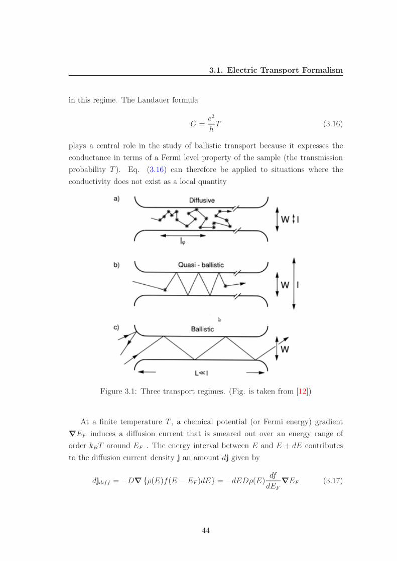
3.1. Electric Transport Formalism
in this regime. The Landauer formula
G =e2
hT (3.16)
plays a central role in the study of ballistic transport because it expresses the
conductance in terms of a Fermi level property of the sample (the transmission
probability T ). Eq. (3.16) can therefore be applied to situations where the
conductivity does not exist as a local quantity
Figure 3.1: Three transport regimes. (Fig. is taken from [12])
At a finite temperature T , a chemical potential (or Fermi energy) gradient
∇EF induces a diffusion current that is smeared out over an energy range of
order kBT around EF . The energy interval between E and E + dE contributes
to the diffusion current density j an amount dj given by
djdiff = −D∇ ρ(E)f(E − EF )dE = −dEDρ(E)df
dEF∇EF (3.17)
44
3.1. Electric Transport Formalism
where D is the diffusion constant taken at energy E. The integration over E
gives the total diffusion current density:
j = −∇EF e−2
∫ ∞
0
dEσ(E, 0)df
dEF
(3.18)
where σ(E, 0) is the zero temperature conductivity in Eq. (3.11) for a Fermi
energy equal to E. The requirement of vanishing current for a spatially constant
electrochemical potential implies that the conductivity σ(EF , T ) at temperature
T and Fermi energy EF satisfies
σ(EF , T )e−2∇EF + j = 0 (3.19)
Therefore, the finite-temperature conductivity is given simply by the energy av-
erage of the zero-temperature result [12]
σ(EF , T ) =
∫ ∞
0
dEσ(E, 0)df
dEF
(3.20)
As T → 0, df/dEF → δ(E−EF ), so indeed only E = EF contributes to the energy
average. Result (3.20) contains exclusively the effects of a finite temperature
that are due to the thermal smearing of the Fermi-Dirac distribution. A possible
temperature dependence of the scattering processes is not taken into account.
3.1.3 The Kubo-Greenwood Formula
Hereafter, we will briefly derive the Kubo-Greenwood formula for DC conductivity
which will be applied to the real-space calculation to compute the conductivity,
mean free path, mobility...etc. More detail derivation can be seen at Ref. [1]
Let’s consider an electron in an weak electric field pointing along the x direc-
tion
E = E0 cos(ωt)ux (3.21)
The weak vector potential of this field A(t) = − E0
2iω(eiωt − e−iωt)ux will add a
perturbative term δH(t) = 2ePA(t)2m
= −eE0
2iω(eiωt−e−iωt)vx to electron Hamiltonian
H0 which includes any interactions in the absence of electric field.
45
3.1. Electric Transport Formalism
In perturbation theory, the total wavefunction Ψm(t) in the presence of elec-
tric field can be expanded in term nonperturbed wavefunctions ψn: Ψm(t) =∑
n an(t)ψn where the coefficients an(t) can be approximately determined by first-
order perturbation theory. The transition from initial states |n〉 at t = 0 to final
states |m〉 at t in this theory is given by
pnm(t) =1
~2
∣
∣
∣
∣
∫ t
0
dτei(Em−En)τ/~〈m|δH(τ)|n〉∣
∣
∣
∣
2
(3.22)
And the transition rate at long time
pnmt
=2π
~
(
eE0
2ω
)2
|〈m|vx|n〉|2 [δ (Em − (En + ~ω)) + δ(Em − (En − ~ω))]
(3.23)
The first term corresponds to the absorbed transition where electron in the initial
state |n〉 with energy En absorbs an energy ~ω and changes to final state |m〉.Similarly, the second term is emitted transition. Hence the net rate of absorption
of energy (total absorbed power) is given by
P =πe2E2
0
2ω
∑
m,n
|〈m|vx|n〉|2 [δ (Em − (En + ~ω)) − δ(Em − (En − ~ω))] (3.24)
This is absorbed power for isolatedly single electron. When we consider electron
ensemble, we have to take into account the Fermi distribution and the Pauli
exclusion principle and 2 spin components.
P =πe2E2
0
ω
∑
m,n
|〈m|vx|n〉|2 (f(En)(1−f(Em)) [δ (Em − (En + ~ω)) − δ(Em − (En − ~ω))]
(3.25)
After some calculation and index permutation, we obtain
P = π~e2E20
∑
m,n
f(En) − f(Em)
~ω|〈m|vx|n〉|2 δ (Em − (En + ~ω)) (3.26)
On the other hand, the total absorbed is defined as P = 12σ(ω)ΩE2
0 , where
σ(ω) is the conductivity of the system. By substituting this formula into the
46
3.1. Electric Transport Formalism
above equation we obtain
σ(ω) =2πe2~
Ω
∑
m,n
f(En) − f(Em)
~ω|〈m|vx|n〉|2 δ (Em − (En + ~ω)) (3.27)
This expression can be rewriten in below integral
σ(ω) =2πe2~
Ω
∫ ∞
−∞
dEf(E) − f(E + ~ω)
~ω
∑
m,n
|〈m|vx|n〉|2 δ (E + ~ω − Em) δ (E −En)
(3.28)
By inserting delta function into the braket we have
σ(ω) =2πe2~
Ω
∫ ∞
−∞
dEf(E) − f(E + ~ω)
~ωTr[
vxδ(E − H)vxδ(E + ~ω − H)]
(3.29)
We use the Fermi-Dirac distribution function property limω→0f(E)−f(E+~ω)
~ω=
δ(E − EF ). In the limit of zero temperature the DC conductivity is
σDC(E) =2πe2~
ΩTr[
vxδ(E − H)vxδ(E − H)]
(3.30)
where Ω is the volume of the system. The last delta-function is rewritten as an
integral
δ(E − H) =1
2π~
∫ ∞
−∞
dtei(E−H)t/~ (3.31)
and inserted into Eq. (3.30):
σDC(E) =e2
Ω
∫ ∞
−∞
dtTr[
vxδ(E − H)eiEt/~vxe−iHt/~
]
=e2
Ω
∫ ∞
−∞
dtTr[
vx(0)δ(E − H)vx(t)]
(3.32)
Where the final formula is obtained thanks to the delta function δ(E − H) and
vx(t) = eiHt/~vxe−iHt/~ is velocity operator in Heisengberg representation
Now we will show that the formula for the quantum average of any operator
47
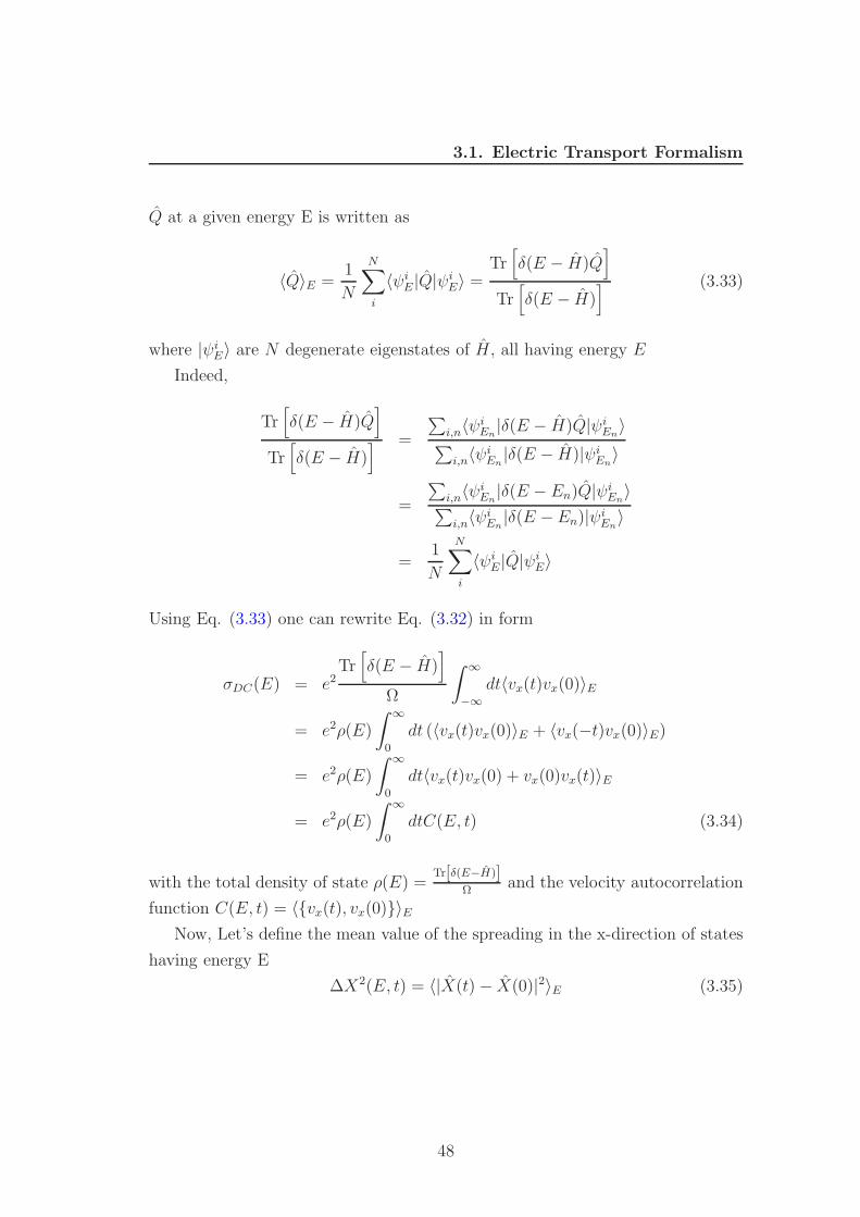
3.1. Electric Transport Formalism
Q at a given energy E is written as
〈Q〉E =1
N
N∑
i
〈ψiE |Q|ψi
E〉 =Tr[
δ(E − H)Q]
Tr[
δ(E − H)] (3.33)
where |ψiE〉 are N degenerate eigenstates of H, all having energy E
Indeed,
Tr[
δ(E − H)Q]
Tr[
δ(E − H)] =
∑
i,n〈ψiEn|δ(E − H)Q|ψi
En〉
∑
i,n〈ψiEn|δ(E − H)|ψi
En〉
=
∑
i,n〈ψiEn|δ(E − En)Q|ψi
En〉
∑
i,n〈ψiEn|δ(E −En)|ψi
En〉
=1
N
N∑
i
〈ψiE |Q|ψi
E〉
Using Eq. (3.33) one can rewrite Eq. (3.32) in form
σDC(E) = e2Tr[
δ(E − H)]
Ω
∫ ∞
−∞
dt〈vx(t)vx(0)〉E
= e2ρ(E)
∫ ∞
0
dt (〈vx(t)vx(0)〉E + 〈vx(−t)vx(0)〉E)
= e2ρ(E)
∫ ∞
0
dt〈vx(t)vx(0) + vx(0)vx(t)〉E
= e2ρ(E)
∫ ∞
0
dtC(E, t) (3.34)
with the total density of state ρ(E) =Tr[δ(E−H)]
Ωand the velocity autocorrelation
function C(E, t) = 〈vx(t), vx(0)〉ENow, Let’s define the mean value of the spreading in the x-direction of states
having energy E
∆X2(E, t) = 〈|X(t) − X(0)|2〉E (3.35)
48
3.1. Electric Transport Formalism
time derivative of the spreading gives
d
dt∆X2(E, t) = 〈vx(t)(X(t) − X(0)) + (X(t) − X(0))vx(t)〉E (3.36)
Changing the time arguments and then taking the derivative allow us to write
the second derivative of ∆X2(E, t) as
d
dt∆X2(E, t) = 〈vx(0)vx(−t) + vx(−t)vx(0)〉E (3.37)
Changing the time arguments again we finally get
d2
dt2∆X2(E, t) = C(E, t) (3.38)
Replacing above equation into Eq. (3.34) we get the final expression for conduc-
tivity which is usually used in the calculation
σ1DC(E) = e2ρ(E) lim
t→∞
d
dt∆X2(E, t) (3.39)
with the spreading of the wavepacket in the x-direction
∆X2(E, t) =
Tr
[
δ(E − H)(
X(t) − X(0))2]
Tr[
δ(E − H)] (3.40)
An alternative definition, in which the derivative in the Eq. (3.39) is replaced by
a division
σ2DC(E) = e2ρ(E)
∆X2(E, t)
t= e2ρ(E)Dx(E, t) (3.41)
is frequently used, because it gives smoother curves for the conductivity than Eq.
(3.39) does.
The similarity of Eq. (3.41) and Eq. (3.11) shows that the diffusion coefficient
is given by
Dx(E, t) =∆X2(E, t)
t(3.42)
49
3.1. Electric Transport Formalism
3.1.4 Three Transport Regimes
As mentioned in Section 3.1.2 with semiclassical approach that the motion of
electron in the sample can be in three different regimes depending on sample size
and disoders. I this section we will discuss more detail about three these regimes
basing on diffusion coefficient Dx(E, t) in above quantum approach.
DE(t
)
(a) Ballistic regime
vSlope:F
2
vF
Slope:
~ t1/2
~ constant
DE(t
)
DE(t
)
XE(t) XE(t)
XE(t)~ constant
~ 1/t
time
time time time
time time
(b) Diffusive regime (c) Localized regime
Figure 3.2: Diffusion coefficient (main frame) and displacement (inset) in threetransport regimes: (a) Ballistic regime, (b) Diffusive regime and (c) Localizedregime
Ballistic regime
In the absence of disoder, structural imperfections or the distance between
the source and drain L is much smaller than mean free path (L ≪ ℓe), electron
propagates in ballistic regime. In this regime electron moves at a constant velocity
vF so the spreading of wave packet ∆X(t) will increase linearly with time t with
the slope of vF , ∆X(t) = vF t. Therefore, the form of the diffusion coefficient
Dx(EF , t) in expression (3.42) is a line with slope v2F , Dx(EF , t) = v2F t (See Fig.
3.2(a)). These lead to the divergence of the long-time conductivity σDC(EF ) in
Eq. (3.39) (Eq. (3.41) is only correct in the diffusive regime)
σDC(EF )bal. = e2ρ(EF ) limt7→∞
d
dt∆X2(EF , t) = 2e2ρ(EF ) lim
t7→∞v2F t (3.43)
50
3.1. Electric Transport Formalism
As pointed out in Ref. [1], this divergence is due to the fact that when deriving
the linear response theory, a finite dissipation source, intrinsic to the sample, is
introduced both physically and mathematically. The ballistic limit is therefore
not well defined in this formalism. However, we can find the agreement between
this method and Landauer-Buttiker formalism in one dimensional (1D) sample.
Indeed, the formulafor for the conductance in Eq. (3.15) for 1D is G = σ/L where
L = 2vF t is the propagating length of wave packet. Using these formulas and Eq.
(3.43) we get
G(EF ) = 2e2ρ1D(EF ) limt→∞
v2F t
L= e2ρ1D(EF )vF =
2e2
h= G0 (3.44)
where the density of states for 1D is ρ1D(EF ) = 1/π~vF and G0 is the conduc-
tance quantum corresponding to the conductance of one conducting channel. If
there are more than one conducting channel cross the Fermi level, the conduc-
tance is proportional to the number of conducting channels, as expected from the
Landauer formula.
Diffusive regime
As mentioned in Section 3.1.2 in semiclassical approach, the diffusion coeffi-
cient converges in diffusive regime to a constant which is proportional to elastic
scattering time (See Eq. (3.12)), Dscdiff = 1
2v2τp. We can obtain a similar formula
for the Kubo approach by considering the Eq. (3.38) with the velocity autocor-
relation function C(E, t) = 2v2x(E)e−t/τp in diffusive regime, this leads to the√t
behaviour of displacement ∆X(E, t) and a constant diffusion coefficient (See Fig.
3.2(b)).
limt7→∞
∆X2(E, t) = 2τp(E)v2x(E)t and limt7→∞
Dx(E, t) 7−→ 2τp(E)v2x(E) (3.45)
The Kubo formula for diffusive regime then gives access to the semiclassical
conductivity (σsc)
σsc(E) = σDC(E)diff = e2ρ(E)Dx(E, t)
σsc(E) = 2e2ρ(E)τp(E)v2x(E) (3.46)
σsc(E) = 2e2ρ(E)vx(E)ℓxe(E)
51
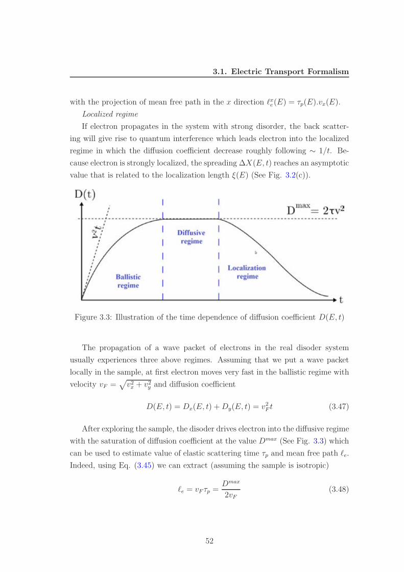
3.1. Electric Transport Formalism
with the projection of mean free path in the x direction ℓxe(E) = τp(E).vx(E).
Localized regime
If electron propagates in the system with strong disorder, the back scatter-
ing will give rise to quantum interference which leads electron into the localized
regime in which the diffusion coefficient decrease roughly following ∼ 1/t. Be-
cause electron is strongly localized, the spreading ∆X(E, t) reaches an asymptotic
value that is related to the localization length ξ(E) (See Fig. 3.2(c)).
Figure 3.3: Illustration of the time dependence of diffusion coefficient D(E, t)
The propagation of a wave packet of electrons in the real disoder system
usually experiences three above regimes. Assuming that we put a wave packet
locally in the sample, at first electron moves very fast in the ballistic regime with
velocity vF =√
v2x + v2y and diffusion coefficient
D(E, t) = Dx(E, t) +Dy(E, t) = v2F t (3.47)
After exploring the sample, the disoder drives electron into the diffusive regime
with the saturation of diffusion coefficient at the value Dmax (See Fig. 3.3) which
can be used to estimate value of elastic scattering time τp and mean free path ℓe.
Indeed, using Eq. (3.45) we can extract (assuming the sample is isotropic)
ℓe = vF τp =Dmax
2vF(3.48)
52
3.1. Electric Transport Formalism
which leads us to following formulas for σsc (See Eq. (3.46))
σsc(E) = σxx =1
2e2ρ0(E)Dmax
x =1
4e2ρ0(E)Dmax
σsc(E) =1
2e2ρ0(E)v2F (E)τp(E) (3.49)
σsc(E) =1
2e2ρ0(E)vF (E)ℓe(E)
with ρ0(E) = 2ρ(E) is the total density of state (the factor of 2 accounts for spin
degeneracy) which is given by Eq. (2.17) for perfect graphene. Electron mobility
µ in this regime is given by
µ(E) =σsc(E)
en(E)(3.50)
where n(E) =∫
ρ0(E)dE is the charge density.
After the diffusive regime, depending on the disoder source, electron might
enter the localization regime due to quantum interference effect. The electrons
start to localize resulting in a decreasing diffusion coefficient. The quantum
interference gives the quantum correction δσ(L) to the semiclassical conductivity
[1]
σ(L) = σsc + δσ(L) with δσ(L) = −2e2
πhln
(
L
ℓe
)
(3.51)
The transition to the insulating state is continuous and reached when the quantum
correction is of the same order of the semiclassical conductivity, that is when
∆σ(L = ξ) ≃ σsc. This let us to extract the localization length ξ
ξ = ℓe exp(πσsc/G0) (3.52)
3.1.5 The Kubo Formalism in Real Space
In this section I will present an efficient real space implementation of the Kubo for-
mula which is mainly used in this thesis to study quantum transport in graphene.
This method was first developed by Roche and Mayou in 1997 for the study of
quasiperiodic systems [99] and was then adapted by Stephan and coworkers to
study electric transport in disordered mesoscopic systems. The advantage of this
method is that the quantum transport of large systems can be investigated thanks
53
3.1. Electric Transport Formalism
to linear-scaling time consuming. The maximum number of orbitals in the system
can be studied at the moment is hundred millions and the simulation of samples
with 1 billion orbitals can be envisioned in the next decade.
There are two major problems one needs to overcome when using the Eq.
(3.41) to calculate the conductivity. The first one is how to change the Eq.
(3.40) to the simpler expression. The second one is how to calculate the trace
without finding the eigenstates of the system.
Let’s find the solution for the first problem by rearranging terms in the ex-
pression (3.40) with the cyclic property of trace.
∆X2(E, t) =Tr[
δ(E − H)∣
∣X(t) − X(0)∣
∣
2]
Tr[
δ(E − H)] (3.53)
∆X2(E, t) =Tr[
(X(t) − X(0))†δ(E − H)(X(t) − X(0))]
Tr[
δ(E − H)] (3.54)
We then use several identities and definitions to rewrite (X(t) − X(0))
X(t) = eiHt~ X(0)e
−iHt~ (3.55)
U(t) = e−iHt
~ (3.56)
where U(t) is the evolution operator,
X(t) − X(0) = U †(t)XU(t) − X (3.57)
X(t) − X(0) = U †(t)XU(t) − U †(t)U(t)X (3.58)
X(t) − X(0) = U †(t)[X, U(t)] (3.59)
using U †(t)U(t) = I, and [· · · , · · · ] the commutator. Then by replacing these
quantities in Eq. (3.54), one gets
54
3.1. Electric Transport Formalism
∆X2(E, t) =Tr[
[X, U(t)]†U(t)δ(E − H)U †(t)[X, U(t)]]
Tr[
δ(E − H)] (3.60)
∆X2(E, t) =Tr[
[X, U(t)]†δ(E − H)[X, U(t)]]
Tr[
δ(E − H)] (3.61)
This is the simplest form of ∆X2(E, t) that we use for the numerical calculation.
Now the next mission is how to evaluate the trace without calculating the
eigenstates of the system which costs a lot of time. The way that we do it is
approximating the trace by expectation values on random phase states which are
expanded on all the orbitals |i〉 of the basis set
|ϕRP 〉 =1√N
N∑
i=1
e2iπαi |i〉, (3.62)
where αi is a random number in the [0, 1] range. An average over few tens of
random phases states is usually sufficient to calculate the expectation values.
Using this stratergy for the expression (3.61), we find
∆X2(E, t) =〈ϕRP |[X, U(t)]†δ(E − H)[X, U(t)]|ϕRP 〉
〈ϕRP |δ(E − H)|ϕRP 〉(3.63)
∆X2(E, t) =〈ϕ′
RP (t)|δ(E − H)|ϕ′RP (t)〉
〈ϕRP |δ(E − H)|ϕRP 〉(3.64)
The numerator and the denominator have the same form. The techniques used
for the computation of the density of states can thus be also employed for the
computation of ∆X2(E, t) provided one first evaluates |ϕ′RP (t)〉 = [X, U(t)]|ϕRP 〉.
The evaluation of |ϕ′RP (t)〉 needs [X, H] together with U(t)|ϕRP 〉 which can be
done by expanding U(t) into the Chebyshev polynomials. The detail techniques
are mentioned in Appendix A. Moreover, the density of state is calculated by the
Lanczos method [100, 101] in which we tridiagonalize the Hamiltonian and then
calculate the density of state in form of continued fraction. The detail techniques
55
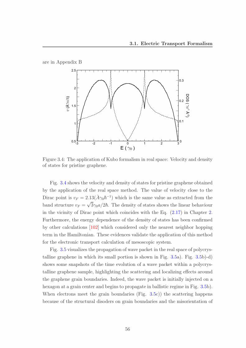
3.1. Electric Transport Formalism
are in Appendix B
E ( )0 1 2 3-1-2-3
0.5
1
1.5
2
2.5
0
0.2
0.1
0.3
(Å / )
DO
S ( -1 Å
-2)
Figure 3.4: The application of Kubo formalism in real space: Velocity and densityof states for pristine graphene.
Fig. 3.4 shows the velocity and density of states for pristine graphene obtained
by the application of the real space method. The value of velocity close to the
Dirac point is vF = 2.13(Aγ0~−1) which is the same value as extracted from the
band structure vF =√
3γ0a/2~. The density of states shows the linear behaviour
in the vicinity of Dirac point which coincides with the Eq. (2.17) in Chapter 2.
Furthermore, the energy dependence of the density of states has been confirmed
by other calculations [102] which considered only the nearest neighbor hopping
term in the Hamiltonian. These evidences validate the application of this method
for the electronic transport calculation of mesoscopic system.
Fig. 3.5 visualizes the propagation of wave packet in the real space of polycrys-
talline graphene in which its small portion is shown in Fig. 3.5a). Fig. 3.5b)-d)
shows some snapshots of the time evolution of a wave packet within a polycrys-
talline graphene sample, highlighting the scattering and localizing effects around
the graphene grain boundaries. Indeed, the wave packet is initially injected on a
hexagon at a grain center and begins to propagate in ballistic regime in Fig. 3.5b).
When electrons meet the grain boundaries (Fig. 3.5c)) the scattering happens
because of the structural disoders on grain boundaries and the misorientation of
56
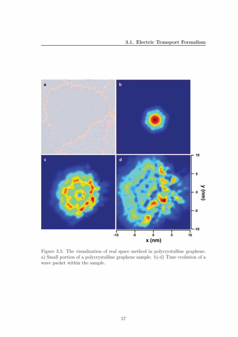
3.1. Electric Transport Formalism
Figure 3.5: The visualization of real space method in polycrystalline graphene.a) Small portion of a polycrystalline graphene sample. b)-d) Time evolution of awave packet within the sample.
57
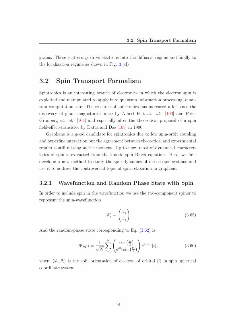
3.2. Spin Transport Formalism
grains. These scatterings drive electrons into the diffusive regime and finally to
the localization regime as shown in Fig. 3.5d)
3.2 Spin Transport Formalism
Spintronics is an interesting branch of electronics in which the electron spin is
exploited and manipulated to apply it to quantum information processing, quan-
tum computation, etc. The research of spintronics has increased a lot since the
discovery of giant magnetoresistance by Albert Fert et. al. [103] and Peter
Grunberg et. al. [104] and especially after the theoretical proposal of a spin
field-effect-transistor by Datta and Das [105] in 1990.
Graphene is a good candidate for spintronics due to low spin-orbit coupling
and hyperfine interaction but the agreement between theoretical and experimental
results is still missing at the moment. Up to now, most of dynamical character-
istics of spin is extracted from the kinetic spin Bloch equation. Here, we first
develope a new method to study the spin dynamics of mesoscopic systems and
use it to address the controversial topic of spin relaxation in graphene.
3.2.1 Wavefunction and Random Phase State with Spin
In order to include spin in the wavefunction we use the two-component spinor to
represent the spin-wavefunction
|Ψ〉 =
(
Ψ↑
Ψ↓
)
(3.65)
And the random-phase state corresponding to Eq. (3.62) is
|ΨRP 〉 =1√N
N∑
i=1
(
cos(
θi2
)
eiΦi sin(
θi2
)
)
e2iπαi |i〉, (3.66)
where (Φi, θi) is the spin orientation of electron of orbital |i〉 in spin spherical
coordinate system
58
3.2. Spin Transport Formalism
Figure 3.6: Spherical coordinate system for spin
3.2.2 Spin Polarization
The spin dynamics of the system is directly related to the time-dependence of
spin polarization which can be given by the expectation value of the spin Pauli
operator.
〈σ(t)〉 = 〈ψ(0)|σ(t)|ψ(0)〉 (3.67)
where σ(t) = eiHt~ σe
−iHt~ is the spin operator in Heisengberg representation.
However, this expectation gives the spin polarization for the whole spectrum
which is not meaningful. Finding the expectation at specific energy is more
important. In order to do so we use the formula for quantum average of any
operator at a given energy in Eq. (3.33).
〈σ(t)〉E =Tr[
δ(E − H)σ(t)]
Tr[
δ(E − H)] =
Tr[
δ(E − H)σ(t) + σ(t)δ(E − H)]
2Tr[
δ(E − H)] (3.68)
Approximating the trace by expectation values on random phase states |ψ(0)〉 =
|ϕRP 〉 is the strategy to get a faster calculation.
σ(E, t) =〈ψ(0)|δ(E − H)σ(t) + σ(t)δ(E − H)|ψ(0)〉
2〈ψ(0)|δ(E − H)|ψ(0)〉(3.69)
=〈ψ(t)|δ(E − H)σ + σδ(E − H)|ψ(t)〉
2〈ψ(0)|δ(E − H)|ψ(0)〉(3.70)
59
3.2. Spin Transport Formalism
where the time evolution of the wavepackets |ψ(t)〉 = e−iHt
~ |ψ(0)〉 is obtained by
solving the time-dependent Schrodinger equation. This is the equation we use for
the calculation of spin polarization.
Let’s denote the quantity in the numerator of Eq. (3.70) as
P(E, t) = 〈ψ(t)|σδ(E − H)|ψ(t)〉 (3.71)
Eq. (3.70) becomes
σ(E, t) =ℜe (P(E, t))
〈ψ(0)|δ(E − H)|ψ(0)〉(3.72)
the denominator is directly proportional to the density of states ρ(E) and can be
computed by the real space method given in Section 3.1.5 while the numerator
can be calculated by including the energy resolution η
P(E, t) = 〈ψ(t)|σδ(E − H)|ψ(t)〉
= 〈ψ(t)|σ 1
2π
[
1
η − i(E − H)+
1
η + i(E − H)
]
|ψ(t)〉
=1
2π
∑
j
〈ψ(t)|σ|φj〉〈φj|[
1
η − i(E − H)+
1
η + i(E − H)
]
|ψ(t)〉
=i
2π
∑
j
µj〈φj|[
1
E + iη − H− 1
E − iη − H
]
|ψ(t)〉
P(E, t) =i
2π
∑
j
µj
[
〈φj|1
z − H|ψ(t)〉 − 〈φj|
1
z∗ − H|ψ(t)〉
]
where µj = 〈ψ(t)|σ|φj〉 with any complete basic set |φj〉 and z = E + iη
By building a orthonormal basis with the Lanczos method (See Appendix B)
beginning with |φ1〉 =|ψ(t)〉 we have
P(E, t) =i
2π
∑
j=1
µj
[
(
1
z −H
)
j,1
−(
1
z∗ −H
)
j,1
]
(3.73)
60
3.2. Spin Transport Formalism
Where H is the tridiagonal matrix of H in the Lanczos basis (See Appendix B)
H = (Hij) =
a1 b1 0 · · ·b1 a2 b2
0 b2 a3 · · ·...
.... . .
(3.74)
3.2.3 Technical Details
Now what we need to do is finding the first column of the inverted matrices z−Hand z∗ −H which we call κ and κ, respectively
(z −H)K = 1 ⇒∑
n
(z −H)mnκn = δm1 (3.75)
The explicit of above equation
(z −H11)κ1 −H12κ2 = 1
−H21κ1 + (z −H22)κ2 −H23κ3 = 0...
−Hn,n−1κn−1 + (z −Hnn)κn −Hn,n+1κn+1 = 0
From κ1 we can get the others
κ2 =(z −H11)κ1 − 1
H12
κ3 =(z −H22)κ2 −H21κ1
H23
...
κn =(z −Hn−1,n−1)κn−1 −Hn−1,n−2κn−2
Hn−1,n
61
3.2. Spin Transport Formalism
We can do the same for κ just by replacing z by z∗. Using the fact that κ1 = κ∗1,
we can show that κj = κ∗j . Finally, we get the formula for Eq. (3.73)
P(E, t) =i
2π
∑
j=1
µj [κj − κj]
P(E, t) = −1
π
∑
j=1
µjℑm (κj) (3.76)
Subtituting this formula into Eq. (3.72) leads to the final expression for spin
polarization
σ(E, t) = − 1
πΩρ(E)
∑
j=1
ℜe(
µj
)
ℑm (κj) (3.77)
62
Chapter 4
Transport in Disordered
Graphene
Ideal crystalline graphene has exotic properties such as remarkably low dimen-
sionality, high mobility and mechanical strength, tunable carrier type and density,
etc. However, as with most other materials, defects are unavoidable during the
preparation of graphene and can play a key role in many observables, and particu-
larly electronic properties. The purpose of this chapter is to discuss the transport
properties of realistic graphene with the increasing of disorder, beginning from
single defects (vacancies) to line defects in polycrystalline graphene and finally
to amorphous graphene, a strongly topological disordered graphene.
4.1 Transport Properties of Graphene With Va-
cancies
4.1.1 Introduction
The electronic transport properties of graphene are known to be very peculiar
with unprecedented manifestations of quantum phenomena as Klein tunneling
[63, 106], weak antilocalization [61, 107], or anomalous quantum Hall effect [108,
109], all driven by a π-Berry phase stemming from graphene sublattice symmetry
and pseudospin degree of freedom [59, 110, 2]. These fascinating properties,
63
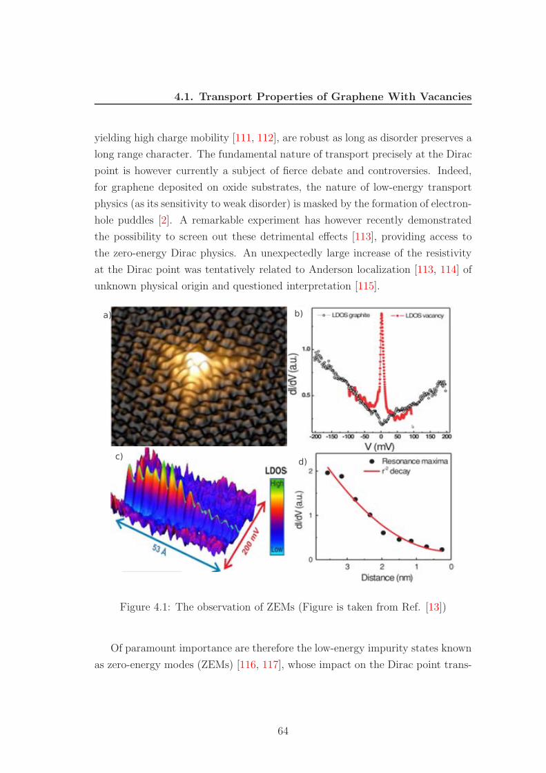
4.1. Transport Properties of Graphene With Vacancies
yielding high charge mobility [111, 112], are robust as long as disorder preserves a
long range character. The fundamental nature of transport precisely at the Dirac
point is however currently a subject of fierce debate and controversies. Indeed,
for graphene deposited on oxide substrates, the nature of low-energy transport
physics (as its sensitivity to weak disorder) is masked by the formation of electron-
hole puddles [2]. A remarkable experiment has however recently demonstrated
the possibility to screen out these detrimental effects [113], providing access to
the zero-energy Dirac physics. An unexpectedly large increase of the resistivity
at the Dirac point was tentatively related to Anderson localization [113, 114] of
unknown physical origin and questioned interpretation [115].
Figure 4.1: The observation of ZEMs (Figure is taken from Ref. [13])
Of paramount importance are therefore the low-energy impurity states known
as zero-energy modes (ZEMs) [116, 117], whose impact on the Dirac point trans-
64
4.1. Transport Properties of Graphene With Vacancies
port physics needs to be clarified. ZEMs are predicted or observed for a variety of
disorder classes, as topological defects (mainly vacancies) [35, 117], adatoms cova-
lently bonded to carbon atoms [118, 119] and extended defects as grain boundaries
[120, 20]. As recently confirmed by scanning tunneling microscopy experiments
on graphene monovacancies [13], ZEMs manifest as wave functions that decay as
the inverse of the distance from the vacancy (See Fig. 4.1), exhibiting a puzzling
quasi-localized character, whose consequences on quantum transport remain to
date highly controversial. First, ZEMs have been predicted to produce a su-
permetallic regime by enhancing the Dirac-point conductivity above its minimum
ballistic value σmin = 4e2/πh [121, 122], an unprecedented conducting state, which
could be in principle explored experimentally [123, 63, 124]. Second, a similar in-
crease of the Dirac point conductivity with defect density has been also reported
in the diffusive regime of two-dimensional disordered graphene in the presence
of vacancies or adatoms [119, 102]. These results contrast with the semiclassical
conductivity found with the Boltzmann approach [125, 35, 126, 127, 128], and
suggest the absence of quantum interferences and localization effects observed
for other types of disorder [72, 129, 130]. Finally, transport experiments in in-
tentionally damaged graphene also report on puzzling conductivity fingerprints,
whose physical origin remains to be fully understood [131, 132]. A comprehen-
sive picture of the role of ZEMs on quantum transport properties in disordered
graphene is therefore crucially missing and demands for further theoretical and
experimental inspection.
This Section provides an extensive analysis of the contribution of zero-energy
modes to quantum conduction close to the Dirac point in disordered graphene.
Using Kubo-Greenwood and Landauer transport approaches, different regimes
are numerically explored by changing the aspect ratio of the transport measure-
ment geometry, and by tuning vacancy density and sublattice symmetry breaking
features. The robustness of the supermetallic state induced by ZEMs is shown to
be restricted to very low densities of compensated vacancies (equally distributed
among both sublattices). This occurs as long as tunneling through evanescent
modes prevails. In the absence of contact effects, an increase of the conductivity
above 4e2/πh is obtained for the semiclassical conductivity at the Dirac point
and ascribed to a high density of ZEMs, but the quantum conductivity analysis
65
4.1. Transport Properties of Graphene With Vacancies
unequivocally reveals a localization regime. For a totally uncompensated vacancy
distribution (populating a single sublattice), the delocalization of ZEMs in real
space is strongly prohibited for a large energy window around the Dirac point
owing to the formation of a gap, whereas no appreciable difference of high en-
ergy transport (above the gap) is found compared with the compensated vacancy
case. I would like to mention that some interesting cases of uncompensated im-
purities and defects have been reported experimentally [133, 134, 135], whose
results demand further exploration.
4.1.2 Zero-Energy Modes and Transport Properties
System description and methodology.- We consider a finite concentration n of
vacancies either distributed at random exclusively on one of the two sublat-
tices (nA = n, the number of vacancies per carbon atoms in sublattice A and
nB = 0, uncompensated case), or equally distributed vacancies on both sub-
lattices (nA = nB = n/2, compensated case). The electronic and transport
properties are investigated by using a tight-binding model with a single pz or-
bital per atom and first nearest neighbor coupling. We model the vacancies by
removing the corresponding orbitals from the Hamiltonian [116, 117]. To investi-
gate the various transport regimes, two complementary approaches are used. For
studying two-dimensional (bulk) disordered graphene, real-space quantum wave
packet dynamics and Kubo conductivity are calculated [72, 99, 136, 137, 129, 4].
The zero-frequency conductivity σ(E, t) for energy E and time t is given by Eq.
(3.41). The diffusion coefficient D(E, t) obtained by using Eq. (3.42) generally
starts with a short-time ballistic motion followed by a saturation regime, which
allows us to estimate the transport (elastic) mean free path ℓe and the semi-
classical conductivity σsc from its maximum value as mentioned in Section 3.1.4.
Depending on disorder strength, D(E, t) is found to decay at longer times owing
to quantum interferences, whose strength may dictate weak or strong (Anderson)
localization at the considered time scale. Calculations are performed for systems
containing several millions of carbon atoms, allowing the capture of all relevant
transport regimes. We also study the ballistic limit of transport through finite
graphene samples, by considering strip geometries with width W and length L
66
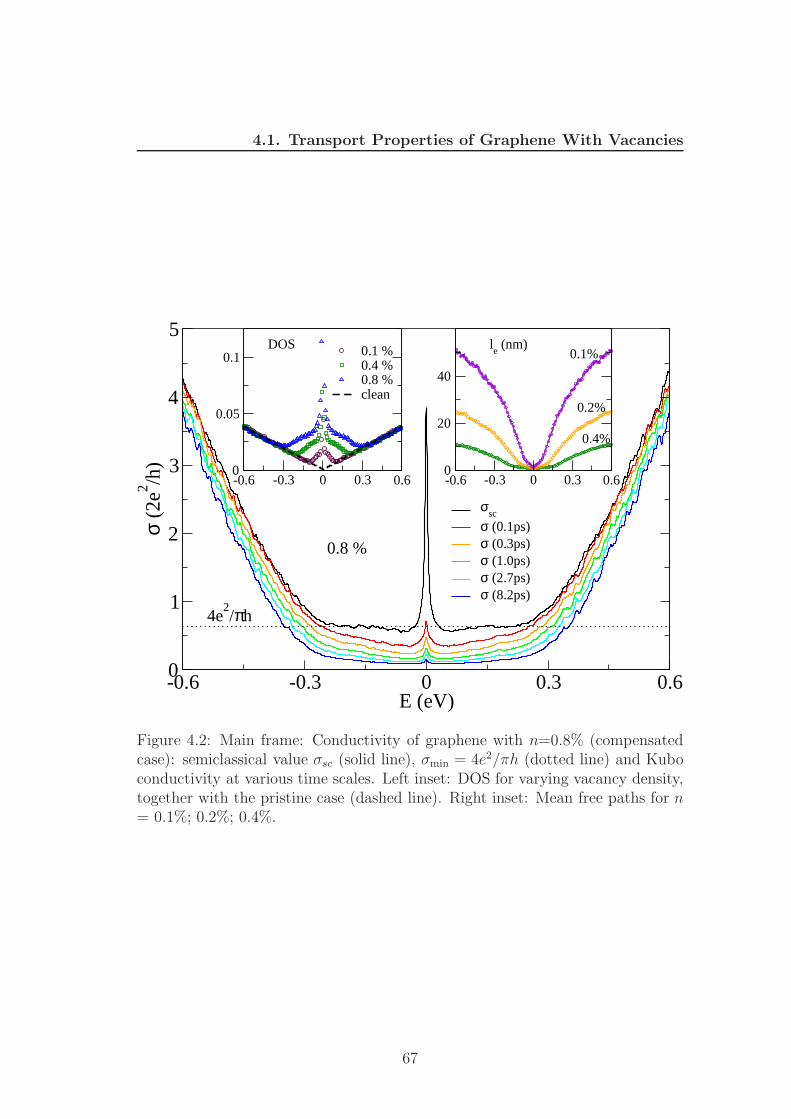
4.1. Transport Properties of Graphene With Vacancies
-0.6 -0.3 0 0.3 0.6E (eV)
0
1
2
3
4
5
σ (2
e2 /h)
σsc
σ (0.1ps)σ (0.3ps)σ (1.0ps) σ (2.7ps) σ (8.2ps)
-0.6 -0.3 0 0.3 0.60
0.05
0.1 0.1 %0.4 %0.8 %clean
-0.6 -0.3 0 0.3 0.60
20
40
4e2/πh
0.8 %
0.1%
0.2%
0.4%
le (nm)DOS
Figure 4.2: Main frame: Conductivity of graphene with n=0.8% (compensatedcase): semiclassical value σsc (solid line), σmin = 4e2/πh (dotted line) and Kuboconductivity at various time scales. Left inset: DOS for varying vacancy density,together with the pristine case (dashed line). Right inset: Mean free paths for n= 0.1%; 0.2%; 0.4%.
67
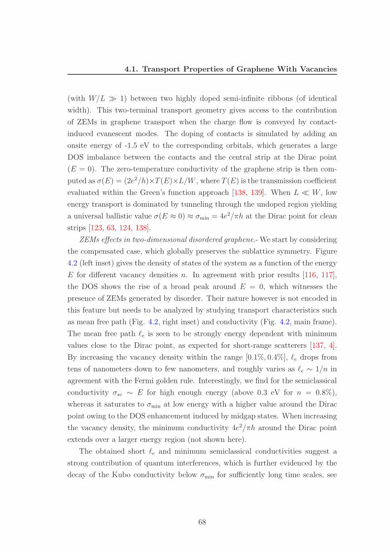
4.1. Transport Properties of Graphene With Vacancies
(with W/L ≫ 1) between two highly doped semi-infinite ribbons (of identical
width). This two-terminal transport geometry gives access to the contribution
of ZEMs in graphene transport when the charge flow is conveyed by contact-
induced evanescent modes. The doping of contacts is simulated by adding an
onsite energy of -1.5 eV to the corresponding orbitals, which generates a large
DOS imbalance between the contacts and the central strip at the Dirac point
(E = 0). The zero-temperature conductivity of the graphene strip is then com-
puted as σ(E) = (2e2/h)×T (E)×L/W , where T (E) is the transmission coefficient
evaluated within the Green’s function approach [138, 139]. When L ≪ W , low
energy transport is dominated by tunneling through the undoped region yielding
a universal ballistic value σ(E ≈ 0) ≈ σmin = 4e2/πh at the Dirac point for clean
strips [123, 63, 124, 138].
ZEMs effects in two-dimensional disordered graphene.- We start by considering
the compensated case, which globally preserves the sublattice symmetry. Figure
4.2 (left inset) gives the density of states of the system as a function of the energy
E for different vacancy densities n. In agreement with prior results [116, 117],
the DOS shows the rise of a broad peak around E = 0, which witnesses the
presence of ZEMs generated by disorder. Their nature however is not encoded in
this feature but needs to be analyzed by studying transport characteristics such
as mean free path (Fig. 4.2, right inset) and conductivity (Fig. 4.2, main frame).
The mean free path ℓe is seen to be strongly energy dependent with minimum
values close to the Dirac point, as expected for short-range scatterers [137, 4].
By increasing the vacancy density within the range [0.1%, 0.4%], ℓe drops from
tens of nanometers down to few nanometers, and roughly varies as ℓe ∼ 1/n in
agreement with the Fermi golden rule. Interestingly, we find for the semiclassical
conductivity σsc ∼ E for high enough energy (above 0.3 eV for n = 0.8%),
whereas it saturates to σmin at low energy with a higher value around the Dirac
point owing to the DOS enhancement induced by midgap states. When increasing
the vacancy density, the minimum conductivity 4e2/πh around the Dirac point
extends over a larger energy region (not shown here).
The obtained short ℓe and minimum semiclassical conductivities suggest a
strong contribution of quantum interferences, which is further evidenced by the
decay of the Kubo conductivity below σmin for sufficiently long time scales, see
68
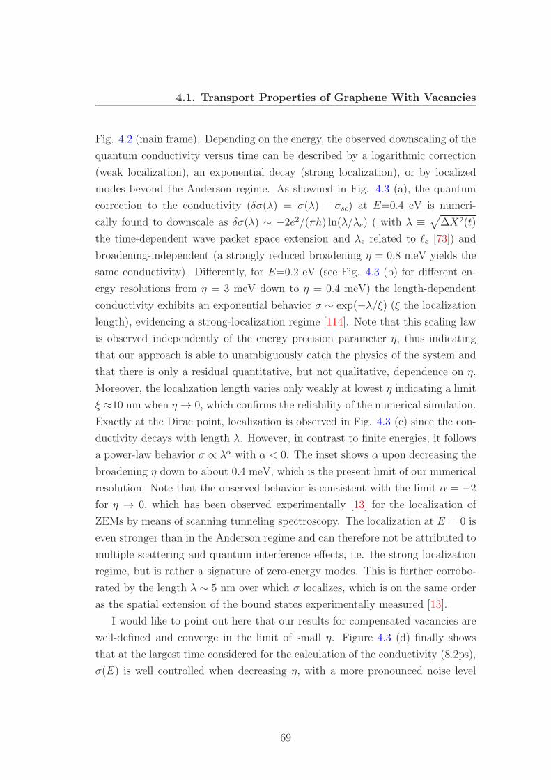
4.1. Transport Properties of Graphene With Vacancies
Fig. 4.2 (main frame). Depending on the energy, the observed downscaling of the
quantum conductivity versus time can be described by a logarithmic correction
(weak localization), an exponential decay (strong localization), or by localized
modes beyond the Anderson regime. As showned in Fig. 4.3 (a), the quantum
correction to the conductivity (δσ(λ) = σ(λ) − σsc) at E=0.4 eV is numeri-
cally found to downscale as δσ(λ) ∼ −2e2/(πh) ln(λ/λe) ( with λ ≡√
∆X2(t)
the time-dependent wave packet space extension and λe related to ℓe [73]) and
broadening-independent (a strongly reduced broadening η = 0.8 meV yields the
same conductivity). Differently, for E=0.2 eV (see Fig. 4.3 (b) for different en-
ergy resolutions from η = 3 meV down to η = 0.4 meV) the length-dependent
conductivity exhibits an exponential behavior σ ∼ exp(−λ/ξ) (ξ the localization
length), evidencing a strong-localization regime [114]. Note that this scaling law
is observed independently of the energy precision parameter η, thus indicating
that our approach is able to unambiguously catch the physics of the system and
that there is only a residual quantitative, but not qualitative, dependence on η.
Moreover, the localization length varies only weakly at lowest η indicating a limit
ξ ≈10 nm when η → 0, which confirms the reliability of the numerical simulation.
Exactly at the Dirac point, localization is observed in Fig. 4.3 (c) since the con-
ductivity decays with length λ. However, in contrast to finite energies, it follows
a power-law behavior σ ∝ λα with α < 0. The inset shows α upon decreasing the
broadening η down to about 0.4 meV, which is the present limit of our numerical
resolution. Note that the observed behavior is consistent with the limit α = −2
for η → 0, which has been observed experimentally [13] for the localization of
ZEMs by means of scanning tunneling spectroscopy. The localization at E = 0 is
even stronger than in the Anderson regime and can therefore not be attributed to
multiple scattering and quantum interference effects, i.e. the strong localization
regime, but is rather a signature of zero-energy modes. This is further corrobo-
rated by the length λ ∼ 5 nm over which σ localizes, which is on the same order
as the spatial extension of the bound states experimentally measured [13].
I would like to point out here that our results for compensated vacancies are
well-defined and converge in the limit of small η. Figure 4.3 (d) finally shows
that at the largest time considered for the calculation of the conductivity (8.2ps),
σ(E) is well controlled when decreasing η, with a more pronounced noise level
69
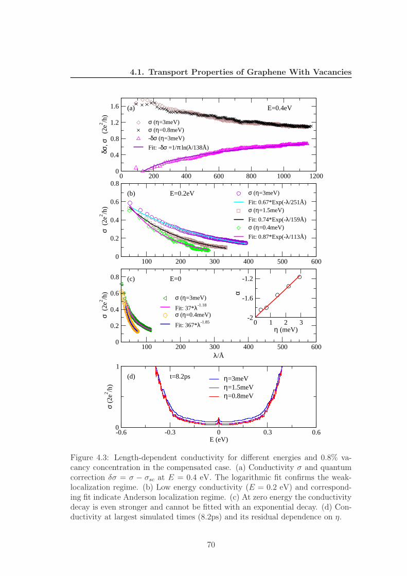
4.1. Transport Properties of Graphene With Vacancies
0 200 400 600 800 1000 12000
0.4
0.8
1.2
1.6δσ
, σ
(2e2 /h
)
σ (η=3meV)σ (η=0.8meV)-δσ (η=3meV)
Fit: -δσ =1/π ln(λ/138Å)
100 200 300 400 500 6000
0.2
0.4
0.6
0.8
σ (
2e2 /h
)
σ (η=3meV)
Fit: 0.67*Exp(-λ/251Å)σ (η=1.5meV)
Fit: 0.74*Exp(-λ/159Å)σ (η=0.4meV)
Fit: 0.87*Exp(-λ/113Å)
100 200 300 400 500 600λ/Å
0
0.2
0.4
0.6
0.8
σ (
2e2 /h
)
σ (η=3meV)
Fit: 37*λ-1.18
σ (η=0.4meV)
Fit: 367*λ-1.85 0 1 2 3η (meV)
-2
-1.6
-1.2
α
-0.6 -0.3 0 0.3 0.6E (eV)
0
1
σ (2
e2 /h)
η=3meVη=1.5meVη=0.8meV
E=0
E=0.4eV
E=0.2eV
(a)
(b)
(c)
(d) t=8.2ps
Figure 4.3: Length-dependent conductivity for different energies and 0.8% va-cancy concentration in the compensated case. (a) Conductivity σ and quantumcorrection δσ = σ − σsc at E = 0.4 eV. The logarithmic fit confirms the weak-localization regime. (b) Low energy conductivity (E = 0.2 eV) and correspond-ing fit indicate Anderson localization regime. (c) At zero energy the conductivitydecay is even stronger and cannot be fitted with an exponential decay. (d) Con-ductivity at largest simulated times (8.2ps) and its residual dependence on η.
70
4.1. Transport Properties of Graphene With Vacancies
-0.6 -0.3 0 0.3 0.6E (eV)
0
1
2
3
4
5
σ (2
e2 /h)
σsc
σ(0.1ps)σ(0.3ps)σ(1.0ps)σ(2.7ps)σ(8.2ps)
-0.4 -0.2 0 0.2 0.4E (eV)
0
0.05
DO
S (
a.u.
) cleanη=0.8meVη=3meV
0 1 2 3 4t (ps)
0.001
0.01
0.1
1
D (
nm2 /fs
)
AB, E=0.5eVAA, E=0.5eVAB, E=0AA, E=0
0.8 % gap gap
gap gap
0.8%
0.8%
Figure 4.4: Main frame: σsc(E) and σ(E, t) for graphene (uncompensated case)and energy resolution η = 3 meV. Left inset: DOS with energy gap revealed byη scaling and ZEMs. Right inset: Diffusion coefficients at E = 0.5 eV and E = 0(η = 3 meV) for both compensated (AB) and uncompensated (AA) cases. Alldata for n = 0.8%
71
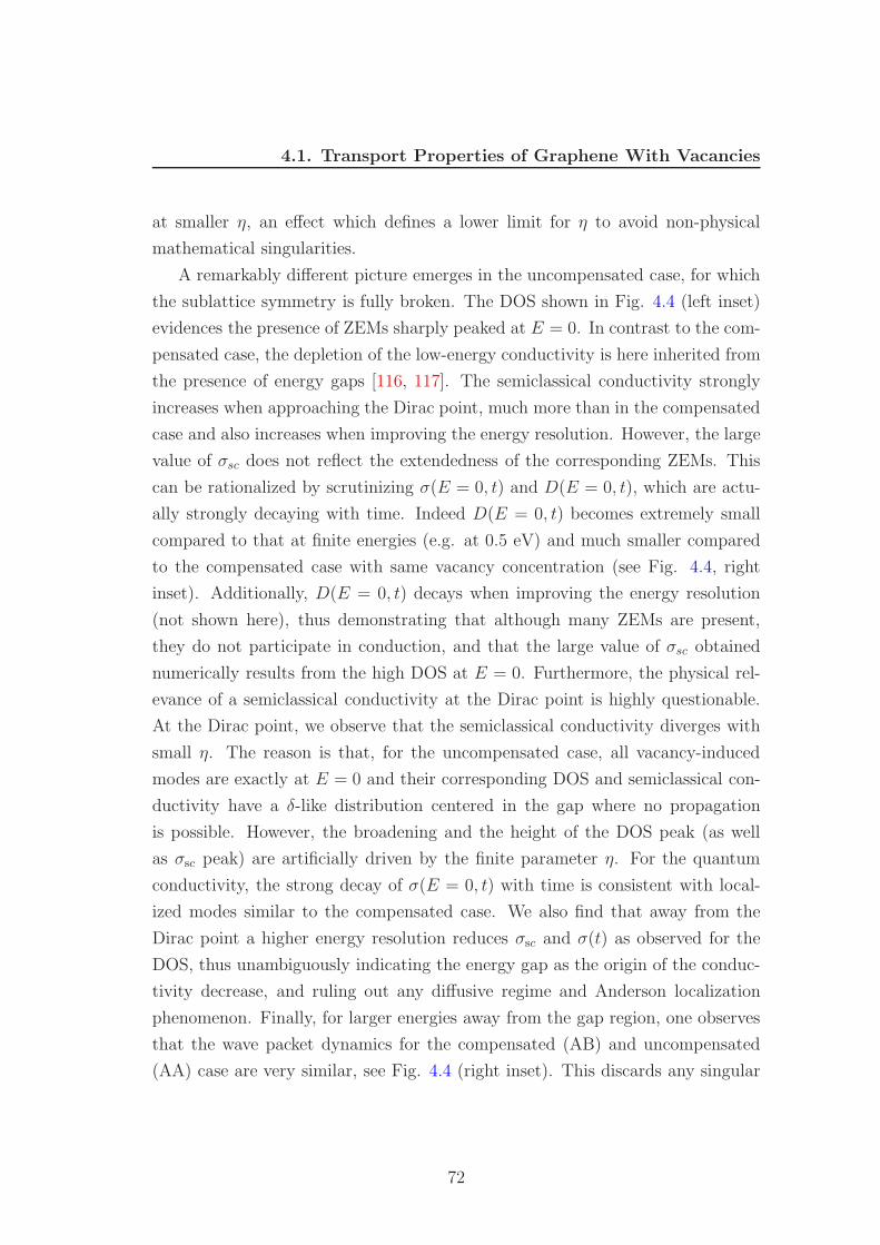
4.1. Transport Properties of Graphene With Vacancies
at smaller η, an effect which defines a lower limit for η to avoid non-physical
mathematical singularities.
A remarkably different picture emerges in the uncompensated case, for which
the sublattice symmetry is fully broken. The DOS shown in Fig. 4.4 (left inset)
evidences the presence of ZEMs sharply peaked at E = 0. In contrast to the com-
pensated case, the depletion of the low-energy conductivity is here inherited from
the presence of energy gaps [116, 117]. The semiclassical conductivity strongly
increases when approaching the Dirac point, much more than in the compensated
case and also increases when improving the energy resolution. However, the large
value of σsc does not reflect the extendedness of the corresponding ZEMs. This
can be rationalized by scrutinizing σ(E = 0, t) and D(E = 0, t), which are actu-
ally strongly decaying with time. Indeed D(E = 0, t) becomes extremely small
compared to that at finite energies (e.g. at 0.5 eV) and much smaller compared
to the compensated case with same vacancy concentration (see Fig. 4.4, right
inset). Additionally, D(E = 0, t) decays when improving the energy resolution
(not shown here), thus demonstrating that although many ZEMs are present,
they do not participate in conduction, and that the large value of σsc obtained
numerically results from the high DOS at E = 0. Furthermore, the physical rel-
evance of a semiclassical conductivity at the Dirac point is highly questionable.
At the Dirac point, we observe that the semiclassical conductivity diverges with
small η. The reason is that, for the uncompensated case, all vacancy-induced
modes are exactly at E = 0 and their corresponding DOS and semiclassical con-
ductivity have a δ-like distribution centered in the gap where no propagation
is possible. However, the broadening and the height of the DOS peak (as well
as σsc peak) are artificially driven by the finite parameter η. For the quantum
conductivity, the strong decay of σ(E = 0, t) with time is consistent with local-
ized modes similar to the compensated case. We also find that away from the
Dirac point a higher energy resolution reduces σsc and σ(t) as observed for the
DOS, thus unambiguously indicating the energy gap as the origin of the conduc-
tivity decrease, and ruling out any diffusive regime and Anderson localization
phenomenon. Finally, for larger energies away from the gap region, one observes
that the wave packet dynamics for the compensated (AB) and uncompensated
(AA) case are very similar, see Fig. 4.4 (right inset). This discards any singular
72
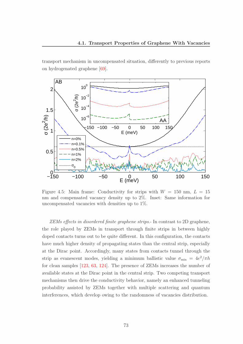
4.1. Transport Properties of Graphene With Vacancies
transport mechanism in uncompensated situation, differently to previous reports
on hydrogenated graphene [69].
E (meV)
σ (2
e2 /h)
−150 −100 −50 0 50 100 1500
0.5
1
1.5
2
n=0%n=0.1%n=0.5%n=1%n=2%
σ0
σ (2
e2 /h)
E (meV)−150 −100 −50 0 50 100 150
10−6
10−4
10−2
100
AB
AA
Figure 4.5: Main frame: Conductivity for strips with W = 150 nm, L = 15nm and compensated vacancy density up to 2%. Inset: Same information foruncompensated vacancies with densities up to 1%.
ZEMs effects in disordered finite graphene strips.- In contrast to 2D graphene,
the role played by ZEMs in transport through finite strips in between highly
doped contacts turns out to be quite different. In this configuration, the contacts
have much higher density of propagating states than the central strip, especially
at the Dirac point. Accordingly, many states from contacts tunnel through the
strip as evanescent modes, yielding a minimum ballistic value σmin = 4e2/πh
for clean samples [123, 63, 124]. The presence of ZEMs increases the number of
available states at the Dirac point in the central strip. Two competing transport
mechanisms then drive the conductivity behavior, namely an enhanced tunneling
probability assisted by ZEMs together with multiple scattering and quantum
interferences, which develop owing to the randomness of vacancies distribution.
73
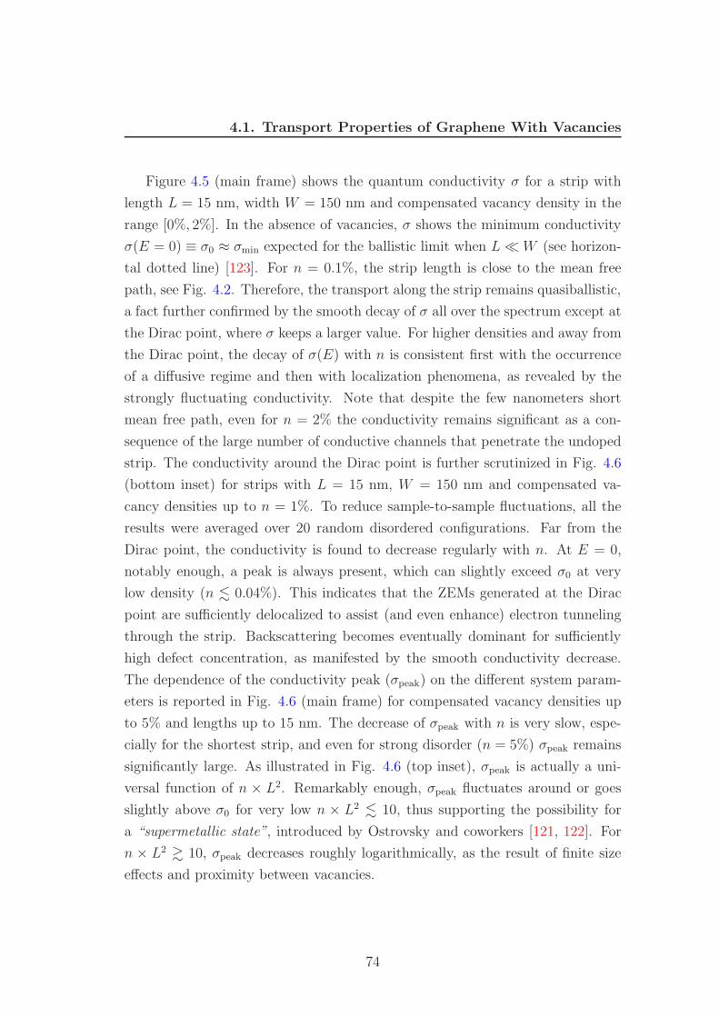
4.1. Transport Properties of Graphene With Vacancies
Figure 4.5 (main frame) shows the quantum conductivity σ for a strip with
length L = 15 nm, width W = 150 nm and compensated vacancy density in the
range [0%, 2%]. In the absence of vacancies, σ shows the minimum conductivity
σ(E = 0) ≡ σ0 ≈ σmin expected for the ballistic limit when L≪W (see horizon-
tal dotted line) [123]. For n = 0.1%, the strip length is close to the mean free
path, see Fig. 4.2. Therefore, the transport along the strip remains quasiballistic,
a fact further confirmed by the smooth decay of σ all over the spectrum except at
the Dirac point, where σ keeps a larger value. For higher densities and away from
the Dirac point, the decay of σ(E) with n is consistent first with the occurrence
of a diffusive regime and then with localization phenomena, as revealed by the
strongly fluctuating conductivity. Note that despite the few nanometers short
mean free path, even for n = 2% the conductivity remains significant as a con-
sequence of the large number of conductive channels that penetrate the undoped
strip. The conductivity around the Dirac point is further scrutinized in Fig. 4.6
(bottom inset) for strips with L = 15 nm, W = 150 nm and compensated va-
cancy densities up to n = 1%. To reduce sample-to-sample fluctuations, all the
results were averaged over 20 random disordered configurations. Far from the
Dirac point, the conductivity is found to decrease regularly with n. At E = 0,
notably enough, a peak is always present, which can slightly exceed σ0 at very
low density (n . 0.04%). This indicates that the ZEMs generated at the Dirac
point are sufficiently delocalized to assist (and even enhance) electron tunneling
through the strip. Backscattering becomes eventually dominant for sufficiently
high defect concentration, as manifested by the smooth conductivity decrease.
The dependence of the conductivity peak (σpeak) on the different system param-
eters is reported in Fig. 4.6 (main frame) for compensated vacancy densities up
to 5% and lengths up to 15 nm. The decrease of σpeak with n is very slow, espe-
cially for the shortest strip, and even for strong disorder (n = 5%) σpeak remains
significantly large. As illustrated in Fig. 4.6 (top inset), σpeak is actually a uni-
versal function of n × L2. Remarkably enough, σpeak fluctuates around or goes
slightly above σ0 for very low n × L2 . 10, thus supporting the possibility for
a “supermetallic state”, introduced by Ostrovsky and coworkers [121, 122]. For
n × L2 & 10, σpeak decreases roughly logarithmically, as the result of finite size
effects and proximity between vacancies.
74
4.1. Transport Properties of Graphene With Vacancies
n (%)
σ peak
(σ 0)
0 0.5 1 1.5 2 2.5 3 3.5 4 4.5 50
0.5
1
1.5L=5 nmL=10 nmL=15 nm
n×L2
σ peak
(σ 0)
0.1 1 10 1000
0.5
1
E (meV)
σ (σ
0)
−10 0 100.2
0.4
0.6
0.8
1
0%
0.04%
0.06%
0.1%
0.3%
0.5%
1%
logarithmic decay
fluctuations around σ0
Figure 4.6: Main frame: Average conductivity peak versus n for strips withW = 150 nm and L = 5, 10 and 15 nm. The shaded areas around the curvesindicate the standard deviation with respect to the average value. Top inset:Same as main frame but as a function of n×L2. The thick straight line is a guideto the eye. Bottom inset: Average conductivity for W = 150 nm, L = 15 nm andvarious n.
75
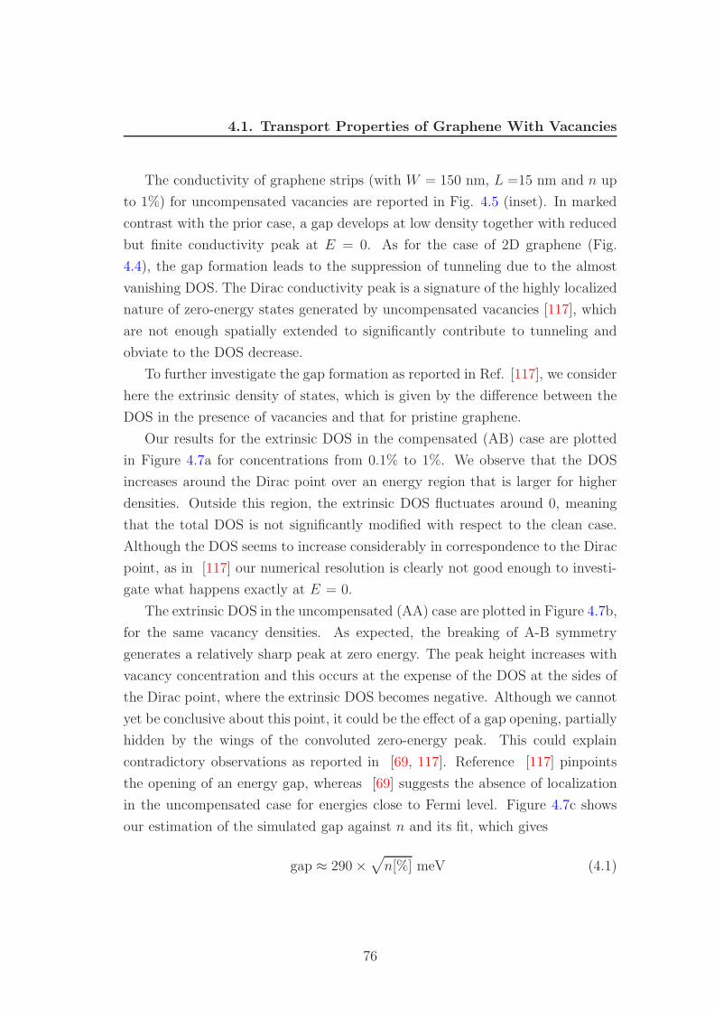
4.1. Transport Properties of Graphene With Vacancies
The conductivity of graphene strips (with W = 150 nm, L =15 nm and n up
to 1%) for uncompensated vacancies are reported in Fig. 4.5 (inset). In marked
contrast with the prior case, a gap develops at low density together with reduced
but finite conductivity peak at E = 0. As for the case of 2D graphene (Fig.
4.4), the gap formation leads to the suppression of tunneling due to the almost
vanishing DOS. The Dirac conductivity peak is a signature of the highly localized
nature of zero-energy states generated by uncompensated vacancies [117], which
are not enough spatially extended to significantly contribute to tunneling and
obviate to the DOS decrease.
To further investigate the gap formation as reported in Ref. [117], we consider
here the extrinsic density of states, which is given by the difference between the
DOS in the presence of vacancies and that for pristine graphene.
Our results for the extrinsic DOS in the compensated (AB) case are plotted
in Figure 4.7a for concentrations from 0.1% to 1%. We observe that the DOS
increases around the Dirac point over an energy region that is larger for higher
densities. Outside this region, the extrinsic DOS fluctuates around 0, meaning
that the total DOS is not significantly modified with respect to the clean case.
Although the DOS seems to increase considerably in correspondence to the Dirac
point, as in [117] our numerical resolution is clearly not good enough to investi-
gate what happens exactly at E = 0.
The extrinsic DOS in the uncompensated (AA) case are plotted in Figure 4.7b,
for the same vacancy densities. As expected, the breaking of A-B symmetry
generates a relatively sharp peak at zero energy. The peak height increases with
vacancy concentration and this occurs at the expense of the DOS at the sides of
the Dirac point, where the extrinsic DOS becomes negative. Although we cannot
yet be conclusive about this point, it could be the effect of a gap opening, partially
hidden by the wings of the convoluted zero-energy peak. This could explain
contradictory observations as reported in [69, 117]. Reference [117] pinpoints
the opening of an energy gap, whereas [69] suggests the absence of localization
in the uncompensated case for energies close to Fermi level. Figure 4.7c shows
our estimation of the simulated gap against n and its fit, which gives
gap ≈ 290 ×√
n[%] meV (4.1)
76
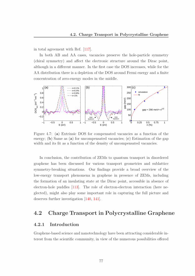
4.2. Charge Transport in Polycrystalline Graphene
in total agreement with Ref. [117].
In both AB and AA cases, vacancies preserve the hole-particle symmetry
(chiral symmetry) and affect the electronic structure around the Dirac point,
although in a different manner. In the first case the DOS increases, while for the
AA distribution there is a depletion of the DOS around Fermi energy and a finite
concentration of zero-energy modes in the middle.
E (eV)
DO
Sex
t (eV
−1 nm
−2 )
−1 −0.5 0 0.5 1
−0.2
0
0.2
0.4
0.6
0.8
1
E (eV)−1 −0.5 0 0.5 1
n (%)ga
p (m
eV)
0 0.25 0.5 0.75 10
50
100
150
200
250
300n=0.1%n=0.4%n=0.8%n=1%
simulationfit
(a) (b) (c)
gap ≈ 290 meV× n1/2
statedepletion
statedepletion
Figure 4.7: (a) Extrinsic DOS for compensated vacancies as a function of theenergy; (b) Same as (a) for uncompensated vacancies; (c) Estimation of the gapwidth and its fit as a function of the density of uncompensated vacancies.
In conclusion, the contribution of ZEMs to quantum transport in disordered
graphene has been discussed for various transport geometries and sublattice
symmetry-breaking situations. Our findings provide a broad overview of the
low-energy transport phenomena in graphene in presence of ZEMs, including
the formation of an insulating state at the Dirac point, accessible in absence of
electron-hole puddles [113]. The role of electron-electron interaction (here ne-
glected), might also play some important role in capturing the full picture and
deserves further investigation [140, 141].
4.2 Charge Transport in Polycrystalline Graphene
4.2.1 Introduction
Graphene-based science and nanotechnology have been attracting considerable in-
terest from the scientific community, in view of the numerous possibilities offered
77
4.2. Charge Transport in Polycrystalline Graphene
by graphene for not only studying fundamental science in two-dimensional (2D)
layered structures [2, 142] but also for improving the performance of flexible mate-
rials and for its integration into a variety of electrical and optical applications.[143,
144, 145, 146, 147, 148, 149] This interest is driven by graphenes superior me-
chanical strength and stiffness,[150] electronic and thermal conductivity,[151, 152]
transparency,[153] and its potential for straightforward incorporation into current
silicon and plastic technologies. [154, 155]
For large-area graphene, the CVD growth technique is unquestionably the
best candidate for achieving a combination of high structural quality and wafer-
scale growth. [33, 156, 157] Unfortunately, the transfer of graphene to diverse
substrates [158, 159] is still a significant challenge for a plethora of applications,
including (bio)chemical sensing, [160] flexible and transparent electrodes, [33] ef-
ficient organic solar cells, [161] multifunctional carbon-based composites, [155]
and spintronic devices. [162] Considerable effort is also needed for fine-tuning of
the CVD growth process. In particular, the produced graphene is typically poly-
crystalline in nature, consisting of a patchwork of grains with various orientations
and sizes, joined by grain boundaries of irregular shapes. [14, 21] The boundaries
consist of an approximately one-dimensional (1D) distribution of non-hexagonal
rings, [14, 21] and appear as structural defects acting as a source of intrinsic car-
rier scattering, which limits the carrier mobility of wafer-scale graphene materials.
[7]
Graphene grain boundaries (GGBs) also introduce enhanced chemical reac-
tivity. [163] This opens a hitherto unexplored area of research, namely, GGB
engineering of the properties of polycrystalline graphene, with further diversifica-
tion of material performance and functionality. Selective chemical functionaliza-
tion of GGBs with various functional groups and selective adsorption of various
metal particles not only modify the carrier mobility of polycrystalline graphene
but also make it biochemically active, a feature which could be utilized in highly
sensitive biochemical sensors. With the capability of engineering GGBs during
CVD growth and their applications mentioned above, a new multidisciplinary
field of science and engineering can be established. Although graphene oxide is
another category of graphene with strong chemical functionalization, the mate-
rials exist in a powder form and their use is also different from large area CVD-
78
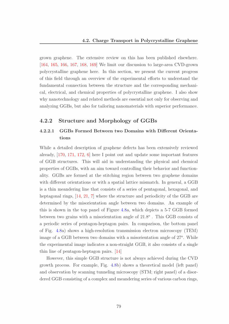
4.2. Charge Transport in Polycrystalline Graphene
grown graphene. The extensive review on this has been published elsewhere.
[164, 165, 166, 167, 168, 169] We limit our discussion to large-area CVD-grown
polycrystalline graphene here. In this section, we present the current progress
of this field through an overview of the experimental efforts to understand the
fundamental connection between the structure and the corresponding mechani-
cal, electrical, and chemical properties of polycrystalline graphene. I also show
why nanotechnology and related methods are essential not only for observing and
analyzing GGBs, but also for tailoring nanomaterials with superior performance.
4.2.2 Structure and Morphology of GGBs
4.2.2.1 GGBs Formed Between two Domains with Different Orienta-
tions
While a detailed description of graphene defects has been extensively reviewed
already, [170, 171, 172, 6] here I point out and update some important features
of GGB structures. This will aid in understanding the physical and chemical
properties of GGBs, with an aim toward controlling their behavior and function-
ality. GGBs are formed at the stitching region between two graphene domains
with different orientations or with a spatial lattice mismatch. In general, a GGB
is a thin meandering line that consists of a series of pentagonal, hexagonal, and
heptagonal rings, [14, 21, 7] where the structure and periodicity of the GGB are
determined by the misorientation angle between two domains. An example of
this is shown in the top panel of Figure 4.8a, which depicts a 5-7 GGB formed
between two grains with a misorientation angle of 21.8o . This GGB consists of
a periodic series of pentagon-heptagon pairs. In comparison, the bottom panel
of Fig. 4.8a) shows a high-resolution transmission electron microscopy (TEM)
image of a GGB between two domains with a misorientation angle of 27o. While
the experimental image indicates a non-straight GGB, it also consists of a single
thin line of pentagon-heptagon pairs. [14]
However, this simple GGB structure is not always achieved during the CVD
growth process. For example, Fig. 4.8b) shows a theoretical model (left panel)
and observation by scanning tunneling microscopy (STM; right panel) of a disor-
dered GGB consisting of a complex and meandering series of various carbon rings,
79
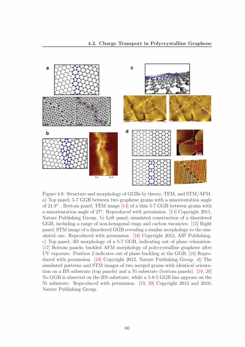
4.2. Charge Transport in Polycrystalline Graphene
Figure 4.8: Structure and morphology of GGBs by theory, TEM, and STM/AFM.a) Top panel; 5-7 GGB between two graphene grains with a misorientation angleof 21.8o . Bottom panel; TEM image [14] of a thin 5-7 GGB between grains witha misorientation angle of 27o. Reproduced with permission. [14] Copyright 2011,Nature Publishing Group. b) Left panel; simulated construction of a disorderedGGB, including a range of non-hexagonal rings and carbon vacancies. [15] Rightpanel; STM image of a disordered GGB revealing a similar morphology to the sim-ulated one. Reproduced with permission. [16] Copyright 2012, AIP Publishing.c) Top panel; 3D morphology of a 5-7 GGB, indicating out of plane relaxation.[17] Bottom panels; buckled AFM morphology of polycrystalline graphene afterUV exposure. Position 2 indicates out of plane buckling at the GGB. [18] Repro-duced with permission. [18] Copyright 2012, Nature Publishing Group. d) Thesimulated patterns and STM images of two merged grains with identical orienta-tion on a BN substrate (top panels) and a Ni substrate (bottom panels). [19, 20]No GGB is observed on the BN substrate, while a 5-8-5 GGB line appears on theNi substrate. Reproduced with permission. [19, 20] Copyright 2013 and 2010,Nature Publishing Group.
80
4.2. Charge Transport in Polycrystalline Graphene
as well as the occasional vacancy defect. [15, 16] In this type of structure, the
electronic effect of the GGB can extend to several nanometers in width, as can be
directly observed from the STM image. Its corresponding transport properties
are independent of the orientation of the two domains forming the GGB. [15]
In order to minimize the structural energy due to the presence of non-hexagonal
rings, the GGB and the surrounding graphene grains can lead to buckling along
the length of the GGB. [17, 18] This is true even in the ideal case, and thus is
a common feature of all GGBs. For example, the top panel of Fig. 4.8c) shows
the morphology of a three-dimensional (3D) model of a GGB and its neighboring
grains, indicating that out-of-plane buckling can occur. The bottom panel of Fig.
4.8c) shows buckled graphene morphology on copper measured before and after
ultraviolet (UV) treatment. [18] The buckling line at position 2 coincides with
the buckled GGB visualized after UV exposure.
The existence of GGBs can strongly alter the mechanical properties of poly-
crystalline graphene. While monocrystalline graphene has been established as
the strongest material ever measured, with an intrinsic strength of 42Nm−1 ,
a failure strain of 0.25, and a Youngs modulus of 1TPa, [150] the mechanical
properties of polycrystalline graphene remain under intense scrutiny. The usual
method for estimating the elastic properties of 2D materials is to transfer the
membrane onto a substrate with an array of holes, and apply a force to the mem-
brane through one of the holes with an atomic force microscope (AFM). [150]
The first reported measurements indicate that GGBs in CVD-grown graphene
significantly lower the elastic constant by a factor of six, [14, 173, 174] with
an average breaking load of about 120nN , an order of magnitude lower than for
monocrystalline graphene. [150] The strength of individual GGBs was also found,
theoretically and experimentally, to strongly depend on the misorientation angle
between graphene domains. [38, 175, 176, 177, 178] However, these results are
for a single GGB between two domains, and it is uncertain how they translate to
macroscopic samples containing several GGBs. Moreover, the cracks that appear
upon failure do not necessarily follow the GGBs but can also penetrate through
the grains, [18, 179] even if they originate at the GGB regions.
A more realistic model for polycrystalline graphene can be constructed by
simulating seeded growth of separated graphene grains with random orientations,
81
4.2. Charge Transport in Polycrystalline Graphene
and allowing such grains to merge together to form natural GGBs. [15] For these
samples, the angle-dependence of the mechanical properties vanishes, and clear
trends appear as a function of the average grain size. Increasing grain sizes lead
to lowering fracture strain and increasing elastic modulus, whereas the variation
in the strength of the material is much less affected, being about 50% of that
of monocrystalline graphene. [15] The cracks originate at GGB junctions, and
propagate through the grains, in agreement with the experiments. [179] More
restricted models containing several connected hexagonal graphene grains have
recently confirmed these findings. [180]
Although much progress has been made in understanding the mechanical
strength of polycrystalline graphene, questions still remain. For example, the
breaking loads for early measurements [14, 174] differ significantly from those
measured more recently. [177, 178] In addition, as noted above, the applicability
of the AFM measurements to macroscopic samples remains an open question. To
finally resolve the issue, we would need a new measurement technique for estimat-
ing the elastic properties of 2D materials, which would avoid the shortcomings of
the method utilizing an AFM tip.
4.2.2.2 GGBs Formed Between two Domains with the Same Orienta-
tion
In addition to degraded mechanical properties, numerous studies have shown
that carrier transport in polycrystalline graphene is strongly affected by GGBs.
[18, 26, 181, 120, 25] Therefore, a great deal of effort has been made to elimi-
nate the formation of GGBs during CVD by growing monocrystalline graphene.
[182, 183, 184, 185, 186, 187] There are two primary methods to obtain monocrys-
talline graphene with CVD. One method is to control the number of nucleation
seeds (and thus the individual grain size) by polishing the copper substrate, [187]
annealing it at high temperature before growth, [182, 183] or using copper ox-
ide. [184, 185] Recently, this approach has been able to realize CVD growth of
individual grains on the order of several millimeters in diameter. The drawback
of this method is that it takes a long time (for instance 12 hours) for a single
graphene grain to grow to a large size. Furthermore, the crystallinity within a
82
4.2. Charge Transport in Polycrystalline Graphene
single domain is not guaranteed or at least not confirmed rigorously. Another
method is based on controlling the orientation of graphene domains, such that
their crystal lattices are aligned. [188, 189, 190, 191] One would then expect that
these domains will merge cleanly, without forming any GGBs at the stitching re-
gions, as shown in the upper left panel of Fig. 4.8d). However, experiments have
shown that this is not always the case. For example, no GGBs were found in the
case of graphene growth on a monocrystalline boron nitride (BN) flake [19] (red
circle, top right panel of Fig. 4.8d). On the other hand, a line of 5 − 8 − 5 rings
was observed for graphene grown on nickel (Ni; bottom panels of Fig. 4.8d) even
though the graphene domains have the same orientation. [20] This is caused by
a translational mismatch between neighboring grains. In addition, non-straight
edges can also lead to more complex GGB structures than the 5− 8− 5 example
shown here. Therefore, additional proof such as high resolution STM, TEM, or
electrical transport measurements are necessary to confirm the absence of GGBs
in these samples. Different methods of observing GGBs are described below.
4.2.3 Methods of Observing GGBs
To study the properties and structure of GGBs, or to control the graphene growth
process, it is necessary to develop methods to determine the location of the GGBs.
This information is not straightforward to obtain due to the atomic width of the
GGBs (on the nm scale), and is even more challenging for large-scale observa-
tions. A primitive approach is to stop the CVD process before graphene growth
is complete. Then, the GGB location can be roughly estimated as the stitching
region between two domains. [187] However, graphene domains are not typi-
cally monocrystalline and thus a large number of GGBs can be missed with this
approach. [18, 26, 187]
Another approach to determine the location of the GGBs relies on mapping
the orientation of the graphene grains; the shape of each grain is identified, and
the GGB locations are then indirectly determined at their boundaries. The tech-
niques for determining the grain orientation include TEM, [14, 21] low electron
energy microscopy, [191] and polarized optical microscopy (POM) of spin-coated
liquid crystals on graphene. [192, 22, 193] However, these methods will not reveal
83
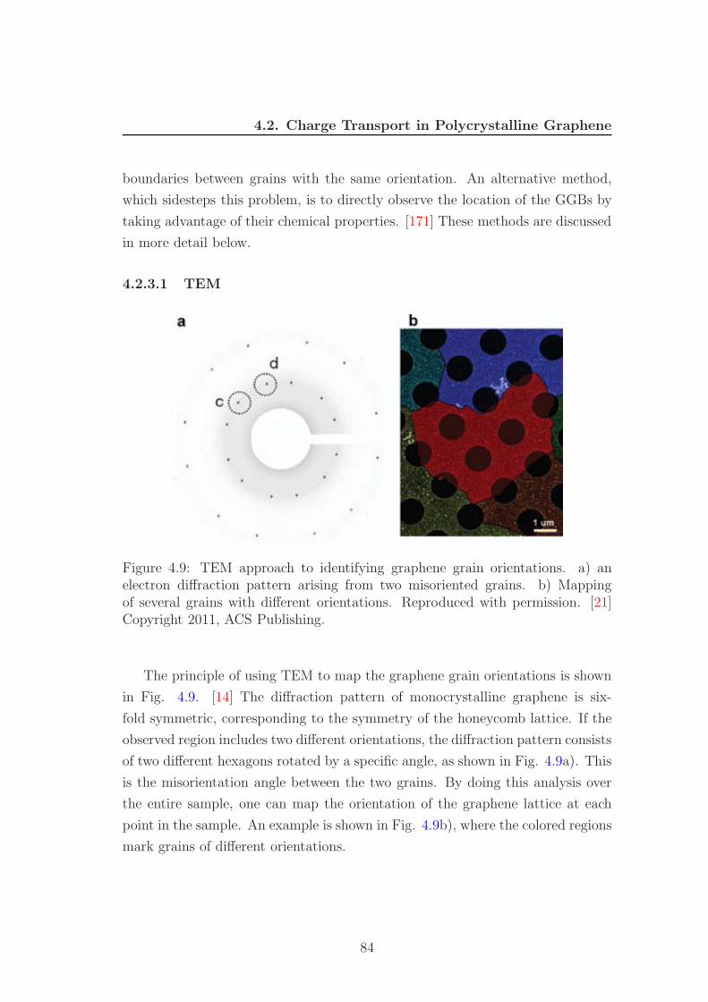
4.2. Charge Transport in Polycrystalline Graphene
boundaries between grains with the same orientation. An alternative method,
which sidesteps this problem, is to directly observe the location of the GGBs by
taking advantage of their chemical properties. [171] These methods are discussed
in more detail below.
4.2.3.1 TEM
Figure 4.9: TEM approach to identifying graphene grain orientations. a) anelectron diffraction pattern arising from two misoriented grains. b) Mappingof several grains with different orientations. Reproduced with permission. [21]Copyright 2011, ACS Publishing.
The principle of using TEM to map the graphene grain orientations is shown
in Fig. 4.9. [14] The diffraction pattern of monocrystalline graphene is six-
fold symmetric, corresponding to the symmetry of the honeycomb lattice. If the
observed region includes two different orientations, the diffraction pattern consists
of two different hexagons rotated by a specific angle, as shown in Fig. 4.9a). This
is the misorientation angle between the two grains. By doing this analysis over
the entire sample, one can map the orientation of the graphene lattice at each
point in the sample. An example is shown in Fig. 4.9b), where the colored regions
mark grains of different orientations.
84
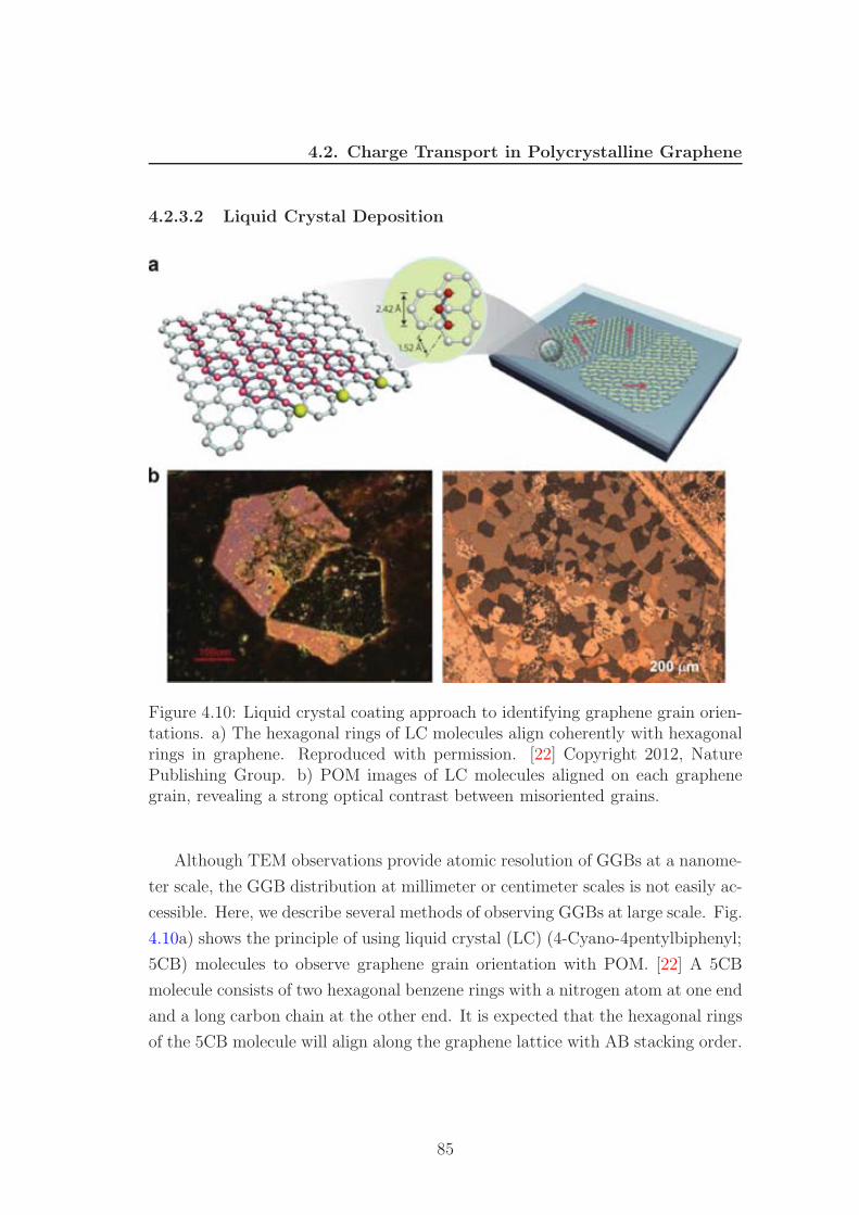
4.2. Charge Transport in Polycrystalline Graphene
4.2.3.2 Liquid Crystal Deposition
Figure 4.10: Liquid crystal coating approach to identifying graphene grain orien-tations. a) The hexagonal rings of LC molecules align coherently with hexagonalrings in graphene. Reproduced with permission. [22] Copyright 2012, NaturePublishing Group. b) POM images of LC molecules aligned on each graphenegrain, revealing a strong optical contrast between misoriented grains.
Although TEM observations provide atomic resolution of GGBs at a nanome-
ter scale, the GGB distribution at millimeter or centimeter scales is not easily ac-
cessible. Here, we describe several methods of observing GGBs at large scale. Fig.
4.10a) shows the principle of using liquid crystal (LC) (4-Cyano-4pentylbiphenyl;
5CB) molecules to observe graphene grain orientation with POM. [22] A 5CB
molecule consists of two hexagonal benzene rings with a nitrogen atom at one end
and a long carbon chain at the other end. It is expected that the hexagonal rings
of the 5CB molecule will align along the graphene lattice with AB stacking order.
85
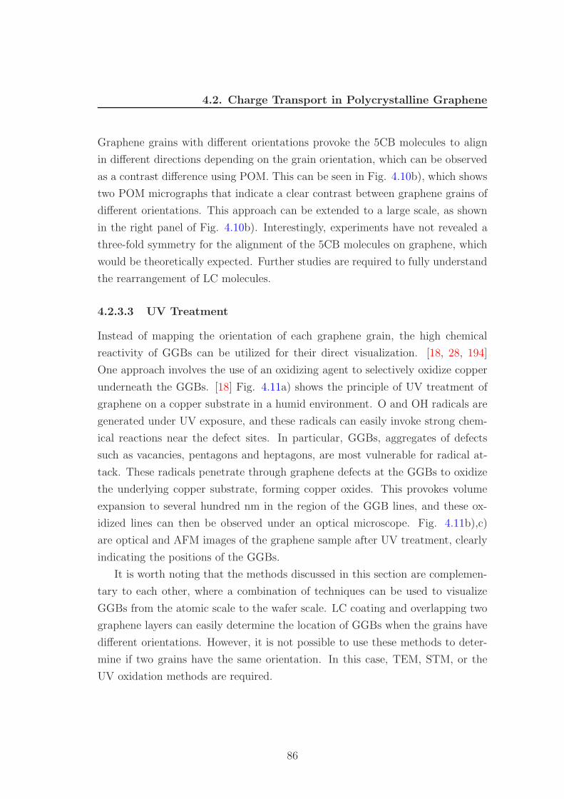
4.2. Charge Transport in Polycrystalline Graphene
Graphene grains with different orientations provoke the 5CB molecules to align
in different directions depending on the grain orientation, which can be observed
as a contrast difference using POM. This can be seen in Fig. 4.10b), which shows
two POM micrographs that indicate a clear contrast between graphene grains of
different orientations. This approach can be extended to a large scale, as shown
in the right panel of Fig. 4.10b). Interestingly, experiments have not revealed a
three-fold symmetry for the alignment of the 5CB molecules on graphene, which
would be theoretically expected. Further studies are required to fully understand
the rearrangement of LC molecules.
4.2.3.3 UV Treatment
Instead of mapping the orientation of each graphene grain, the high chemical
reactivity of GGBs can be utilized for their direct visualization. [18, 28, 194]
One approach involves the use of an oxidizing agent to selectively oxidize copper
underneath the GGBs. [18] Fig. 4.11a) shows the principle of UV treatment of
graphene on a copper substrate in a humid environment. O and OH radicals are
generated under UV exposure, and these radicals can easily invoke strong chem-
ical reactions near the defect sites. In particular, GGBs, aggregates of defects
such as vacancies, pentagons and heptagons, are most vulnerable for radical at-
tack. These radicals penetrate through graphene defects at the GGBs to oxidize
the underlying copper substrate, forming copper oxides. This provokes volume
expansion to several hundred nm in the region of the GGB lines, and these ox-
idized lines can then be observed under an optical microscope. Fig. 4.11b),c)
are optical and AFM images of the graphene sample after UV treatment, clearly
indicating the positions of the GGBs.
It is worth noting that the methods discussed in this section are complemen-
tary to each other, where a combination of techniques can be used to visualize
GGBs from the atomic scale to the wafer scale. LC coating and overlapping two
graphene layers can easily determine the location of GGBs when the grains have
different orientations. However, it is not possible to use these methods to deter-
mine if two grains have the same orientation. In this case, TEM, STM, or the
UV oxidation methods are required.
86
4.2. Charge Transport in Polycrystalline Graphene
Figure 4.11: UV treatment approach to identifying graphene grain orientations.a) Principle of GGB visualization by UV treatment. b-c) Selective oxidationof an underlying the copper substrate for direct optical identification (b) of theGGBs, confirmed by AFM (c). Reproduced with permission. [18] Copyright2012, Nature Publishing Group.
87
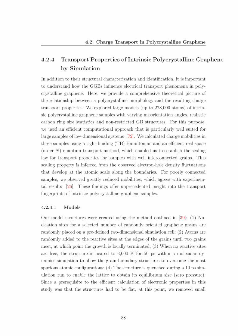
4.2. Charge Transport in Polycrystalline Graphene
4.2.4 Transport Properties of Intrinsic Polycrystalline Graphene
by Simulation
In addition to their structural characterization and identification, it is important
to understand how the GGBs influence electrical transport phenomena in poly-
crystalline graphene. Here, we provide a comprehensive theoretical picture of
the relationship between a polycrystalline morphology and the resulting charge
transport properties. We explored large models (up to 278,000 atoms) of intrin-
sic polycrystalline graphene samples with varying misorientation angles, realistic
carbon ring size statistics and non-restricted GB structures. For this purpose,
we used an efficient computational approach that is particularly well suited for
large samples of low-dimensional systems [72]. We calculated charge mobilities in
these samples using a tight-binding (TB) Hamiltonian and an efficient real space
(order-N) quantum transport method, which enabled us to establish the scaling
law for transport properties for samples with well interconnected grains. This
scaling property is inferred from the observed electron-hole density fluctuations
that develop at the atomic scale along the boundaries. For poorly connected
samples, we observed greatly reduced mobilities, which agrees with experimen-
tal results [26]. These findings offer unprecedented insight into the transport
fingerprints of intrinsic polycrystalline graphene samples.
4.2.4.1 Models
Our model structures were created using the method outlined in [39]: (1) Nu-
cleation sites for a selected number of randomly oriented graphene grains are
randomly placed on a pre-defined two-dimensional simulation cell; (2) Atoms are
randomly added to the reactive sites at the edges of the grains until two grains
meet, at which point the growth is locally terminated; (3) When no reactive sites
are free, the structure is heated to 3,000 K for 50 ps within a molecular dy-
namics simulation to allow the grain boundary structures to overcome the most
spurious atomic configurations; (4) The structure is quenched during a 10 ps sim-
ulation run to enable the lattice to obtain its equilibrium size (zero pressure).
Since a prerequisite to the efficient calculation of electronic properties in this
study was that the structures had to be flat, at this point, we removed small
88
4.2. Charge Transport in Polycrystalline Graphene
corrugations which appeared after the aforementioned preparation steps. To this
end, the structures were repeatedly stretched, gradually forced towards zero in
the third dimension (by scaling down the z-coordinates), and again relaxed (al-
lowing atomic reconstruction at each step), which removed the largest portion
of non-flat configurations. A few remaining non-flat and physically implausible
configurations (overlapping atoms, coordination numbers higher than three) were
removed manually, and a final relaxation and optimization step was carried out.
This resulted in flat structures occupying local energy minima and suitable for
the present study.
a b c
d
incre
asin
g g
rain
siz
e
Figure 4.12: (a) Three structures with uniform grain size distribution and in-creasing average grain sizes (13.0, 18.0 and 25.5 nm). GBs are marked with darklines. (b) Larger magnification of the area marked with a white rectangle in panel(a), showing a typical example of the grain boundaries. Carbon ring-size statis-tics for the same sample (showing the ratio of non-hexagonal rings) are presentedin the upper right corner. (c) Two additional samples with average grain size of18 nm: one sample with broken boundaries (“br-18 nm”) and another one withrandom grain size distribution (“avg-18 nm”). (d) Higher magnification of thearea marked with a white rectangle in panel (c), showing the structure of “bro-ken” boundaries in sample “br-18 nm”. The statistics of non-hexagonal rings areshown in the lower right corner. All scale bars are 10 nm.
89
4.2. Charge Transport in Polycrystalline Graphene
During the sample preparation, the carbon-carbon interactions were modeled
using the reactive bond order potential by Brenner et al. [195] and the tem-
perature and pressure control were handled using the Berendsen method [196].
Most of the structures were approximately 60 × 60 nm2 in size and contained
∼138,000 atoms with the exception of one structure which was significantly larger
(87 × 87 nm2, ∼278,000 atoms). Structure with the smallest grains contained
22 of them, whereas whereas all other structures contained 11 grains. Periodic
boundaries were used in all calculations.
4.2.4.2 The Scaling Law
For electronic and transport calculations, we used a π-π* orthogonal TB model,
described by a single pz-orbital per carbon site, with nearest neighbors hopping
γ0 and zero onsite energies. A distance criterion to search for the first nearest
neighbors was set empirically to 1.15 × aCC, where aCC is the nearest neighbor
distance in pristine graphene. The local fluctuations in bond lengths are small
enough to keep a constant value of γ0 for the transfer integral. The density
of states (DOS) was computed using the Lanczos recursion method with N =
1, 000 recursion steps and an energy resolution η = 0.01γ0 ≃ 0.03 eV. For LDOS
calculations we used the spectral measure operator δ(E − H) projected on state
|i〉 (where i is the site index).
We computed the local charge density deficiency δi (or self-doping) for each
GB site i defined as:
δi =
∫ ECNP
−∞
[ρtot(E) − ρi(E)]dE (4.2)
where ρtot and ρi are the total DOS of the polycrystalline graphene sample and
the LDOS on carbon site i, respectively. ECNP denotes the charge neutrality
point.
To capture the different transport regimes, we employed a real-space order-N
quantum wavepacket evolution approach in Chapter 3 to compute the Kubo-
Greenwood conductivity [72]. As has been shown before [39], our models for
polycrystalline graphene resemble experimentally observed structures: atomic-
resolution and diffraction-filtered electron microscopy experiments have revealed
90
4.2. Charge Transport in Polycrystalline Graphene
that the grains stitch together predominantly via pentagon-heptagon pairs [14,
21, 40] in arrangements of large number of small grains forming an intricate
patchwork interconnected by tilt boundaries [21, 14]. For this study, we created
samples with three different average grain sizes (average diameter 〈d〉 ≈ 13, 18
and 25.5 nm) and uniform grain size distributions (Fig. 4.12a). As seen in
Fig. 4.12b, the atomic structure at the GBs consists predominantly of five-
and seven-membered carbon rings and assumes meandering shapes similar to the
experimentally observed ones. We also created one sample with 〈d〉 ≈ 18 nm
and “broken” (poorly connected) boundaries (“br-18 nm”), and one sample with
〈d〉 ≈ 18 nm and non-uniform d-distribution (“avg-18 nm”) (see Fig. 4.12c,d).
We begin by discussing the electronic density of states (DOS) as a function
of energy (E) for the different samples (Fig. 4.13a). We noticed very little vari-
ation away from charge neutrality point (E = 0), except for a slight broadening
of van Hove singularities at E = ±γ0, where γ0 = −2.9 eV is the nearest neigh-
bor hopping energy. This suggests that GBs induce weak disorder and that the
polycrystalline samples mostly preserve the electron-hole symmetry. However, a
larger difference can be seen at the charge neutrality point (Fig. 4.13b), where all
of the polycrystalline structures show an enhanced density of zero energy modes
[116]. As expected, the largest difference relative to pristine graphene was with
the “br-18 nm” sample (the one with poorly connected grains), reflecting a higher
density of “midgap” states [116, 117].
To better understand the deviations from the pristine graphene for the well-
connected structures, we next identified atoms residing at GBs of the “18 nm”
sample by searching for atoms for which the bond length of at least one nearest
neighbor differs from the carbon spacing in pristine graphene (aCC = 1.42 A) by
0.03 A or more. We then calculated the local charge density deficiency δi (or
self-doping) for each GB site. In Fig. 4.13c we present the atomic structure of
the electron-hole density fluctuations (δi variations greater than 10−4 electrons
per atom) formed at a small area around one GB. These self-doping effects stem
from local fluctuations in the electrostatic potential. Experiments on exfoliated
graphene deposited over silicon dioxide [197, 198] have shown similar potential
inhomogeneities; however, these were spread over a much longer scale (∼ 30 nm)
and were induced by proximity effects generated by charges trapped in the oxide.
91
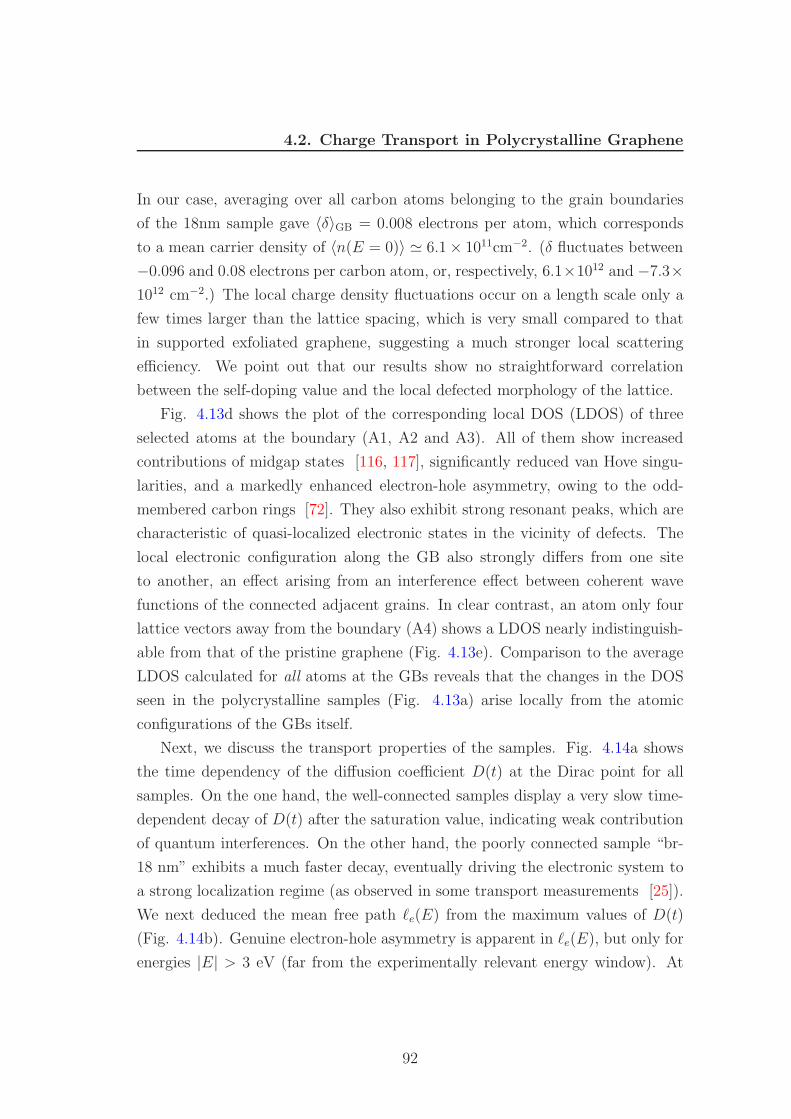
4.2. Charge Transport in Polycrystalline Graphene
In our case, averaging over all carbon atoms belonging to the grain boundaries
of the 18nm sample gave 〈δ〉GB = 0.008 electrons per atom, which corresponds
to a mean carrier density of 〈n(E = 0)〉 ≃ 6.1 × 1011cm−2. (δ fluctuates between
−0.096 and 0.08 electrons per carbon atom, or, respectively, 6.1×10¹² and −7.3×1012 cm−2.) The local charge density fluctuations occur on a length scale only a
few times larger than the lattice spacing, which is very small compared to that
in supported exfoliated graphene, suggesting a much stronger local scattering
efficiency. We point out that our results show no straightforward correlation
between the self-doping value and the local defected morphology of the lattice.
Fig. 4.13d shows the plot of the corresponding local DOS (LDOS) of three
selected atoms at the boundary (A1, A2 and A3). All of them show increased
contributions of midgap states [116, 117], significantly reduced van Hove singu-
larities, and a markedly enhanced electron-hole asymmetry, owing to the odd-
membered carbon rings [72]. They also exhibit strong resonant peaks, which are
characteristic of quasi-localized electronic states in the vicinity of defects. The
local electronic configuration along the GB also strongly differs from one site
to another, an effect arising from an interference effect between coherent wave
functions of the connected adjacent grains. In clear contrast, an atom only four
lattice vectors away from the boundary (A4) shows a LDOS nearly indistinguish-
able from that of the pristine graphene (Fig. 4.13e). Comparison to the average
LDOS calculated for all atoms at the GBs reveals that the changes in the DOS
seen in the polycrystalline samples (Fig. 4.13a) arise locally from the atomic
configurations of the GBs itself.
Next, we discuss the transport properties of the samples. Fig. 4.14a shows
the time dependency of the diffusion coefficient D(t) at the Dirac point for all
samples. On the one hand, the well-connected samples display a very slow time-
dependent decay of D(t) after the saturation value, indicating weak contribution
of quantum interferences. On the other hand, the poorly connected sample “br-
18 nm” exhibits a much faster decay, eventually driving the electronic system to
a strong localization regime (as observed in some transport measurements [25]).
We next deduced the mean free path ℓe(E) from the maximum values of D(t)
(Fig. 4.14b). Genuine electron-hole asymmetry is apparent in ℓe(E), but only for
energies |E| > 3 eV (far from the experimentally relevant energy window). At
92
4.2. Charge Transport in Polycrystalline Graphene
0
0.005
0.010
0.015
0.020
-1.0 -0.5 0 0.5 1.0E (eV)
a b
c dD
OS
(e
V-1
Å-2
)
A1
A2A3
A4
e
0
0.02
0.04
0.06
0.08
0.10
0.12
0.14
-4 -2 0 2 4
PG13 nm18 nm
25.5 nmbr-18 nm
avg-18 nm
E (eV)
DO
S (
eV
-1Å
-2)
DO
S (
eV
-1Å
-2)
0
0.04
0.08
0.12
-10 -5 0 10
E (eV)
PGGBA 4
5
DO
S (
eV
-1Å
-2)
0
0.04
0.08
0.12
-10 -5 0 105
A 1A 2A 3
Figure 4.13: (a) DOS for pristine graphene (PG) and the structures presented inFig. 4.12. (b) Higher magnification of the DOS close to the charge neutralitypoint (E = 0, area marked with a rectangle in panel (a)). (c) Atomic structureof one of the boundaries in sample “18 nm”, showing the electron-hole densityfluctuations at GB sites that develop due to local variations in the charge densityδi: local electron doping (δi < −1 × 10⁻⁴e/atom) is shown in blue and local holedoping (δi > 1 × 10⁻⁴e/atom) in red. (d) Local DOS for atoms A1, A2 and A3marked in panel (c). (e) Local DOS for atom A4 marked in panel (c) as comparedto the average DOS for pristine graphene (PG) and average LDOS for all atomsat GBs in the same sample (GB).
93
4.2. Charge Transport in Polycrystalline Graphene
lower energies around the charge neutrality point (|E| < 1 eV), ℓe(E) changes,
albeit only weakly, for all samples.
The sample with broken boundaries, “br-18 nm”, shows the shortest ℓe <
5 nm and the weakest dependence on energy, except for a pronounced dip at
E = 0. Interestingly, the curves for the two well-connected samples with similar
〈d〉 but different d-distributions (“18 nm” and “avg-18 nm”) are very similar and
clearly different from samples with either smaller or larger grains. However, this
difference can by accounted for by a constant factor. Remarkably, it turns out
that√
2 × ℓ13nme ≈ ℓ18nme and√
2 × ℓ18 nme ≈ ℓ25.5nme (see the scaled values in
Fig. 4.14b), which correspond exactly to the differences in the average grain
sizes in these samples (√
2 × 13 ≈ 18 and√
2 × 18 ≈ 25.5). Moreover, the grain-
size distribution does not enter into this scaling behaviour (ℓ18nme ≈ ℓavg−18nme ).
Hence, we have identified a remarkably simple scaling law that links the average
grain size to transport length scales in polycrystalline graphene with randomly
oriented grains.
The computed semi-classical conductivity σsc(E) exhibits energy-dependent
variations similar to ℓe(E), as can be seen in Fig. 4.14c. We also point out the
linear dependency of ℓe with charge density in the Dirac point vicinity. Again,
the same scaling law (presented above for the mean free path) applies: the ratio
of σsc for two samples with different average grain sizes matches closely with
the ratio of the 〈d〉 values themselves. One additional interesting feature seen
in Fig. 4.14c is that the conductivity remains much higher than the minimum
value 4e2/πh (horizontal line), which fixes the theoretical limit in the diffusive
regime, as derived within the self-consistent Born approximation valid for any
type of disorder [4]. This indicates that polycrystalline graphene remains a good
conductor, even for the poorly connected structure “br-18 nm”.
Localization length of electron states (ξ(E)) can now be estimated using the
values for ℓe and σsc. Scaling analysis (ξ(E) = ℓe(E) exp(πhσsc(E)/2e2) [114])
reveals that ξ ≃ 1 − 10 µm over a large energy window around the charge neu-
trality point. This contrasts with the values (on the order of 10 nm) obtained for
graphene structures with ∼ 1% structural defects, strongly bonded adatoms, or
other types of short range impurities [72, 129].
Finally, we move on to the charge carrier mobility µ(n) (Fig. 4.14d). As
94
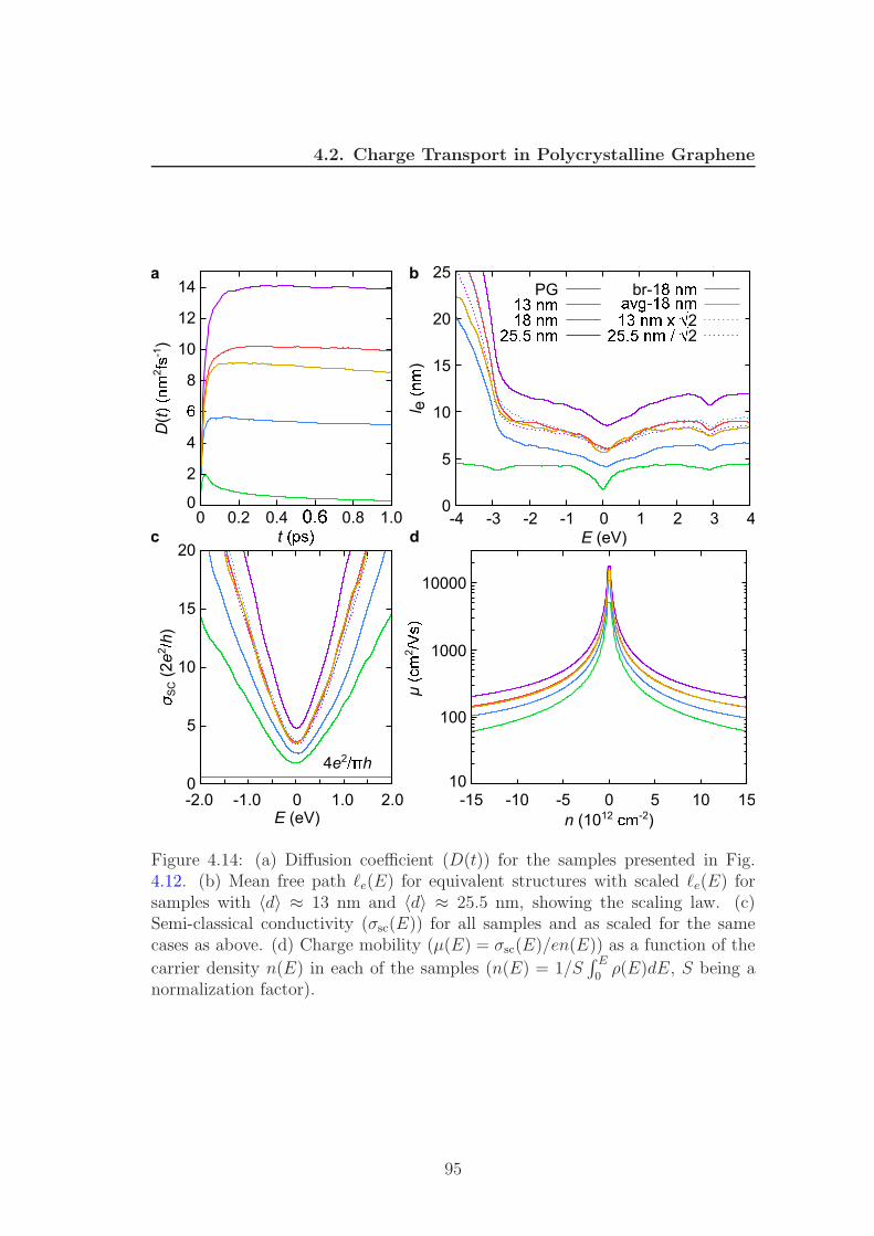
4.2. Charge Transport in Polycrystalline Graphene
10
100
1000
10000
-15 -10 -5 0 5 10 15
µ2
n (1012 -2)
0
2
4
8
10
12
14
0 0.2 0.4 0.8 1.0
D(t
2-1
)
t
ba
c d
0
5
10
15
20
-2.0 -1.0 0 1.0 2.0
SC
(2e
2h)
E (eV)
4e2 h
0
5
10
15
20
25
-4 -3 -2 -1 0 1 2 3 4
l e)
E (eV)
PG br-1
22
Figure 4.14: (a) Diffusion coefficient (D(t)) for the samples presented in Fig.4.12. (b) Mean free path ℓe(E) for equivalent structures with scaled ℓe(E) forsamples with 〈d〉 ≈ 13 nm and 〈d〉 ≈ 25.5 nm, showing the scaling law. (c)Semi-classical conductivity (σsc(E)) for all samples and as scaled for the samecases as above. (d) Charge mobility (µ(E) = σsc(E)/en(E)) as a function of the
carrier density n(E) in each of the samples (n(E) = 1/S∫ E
0ρ(E)dE, S being a
normalization factor).
95
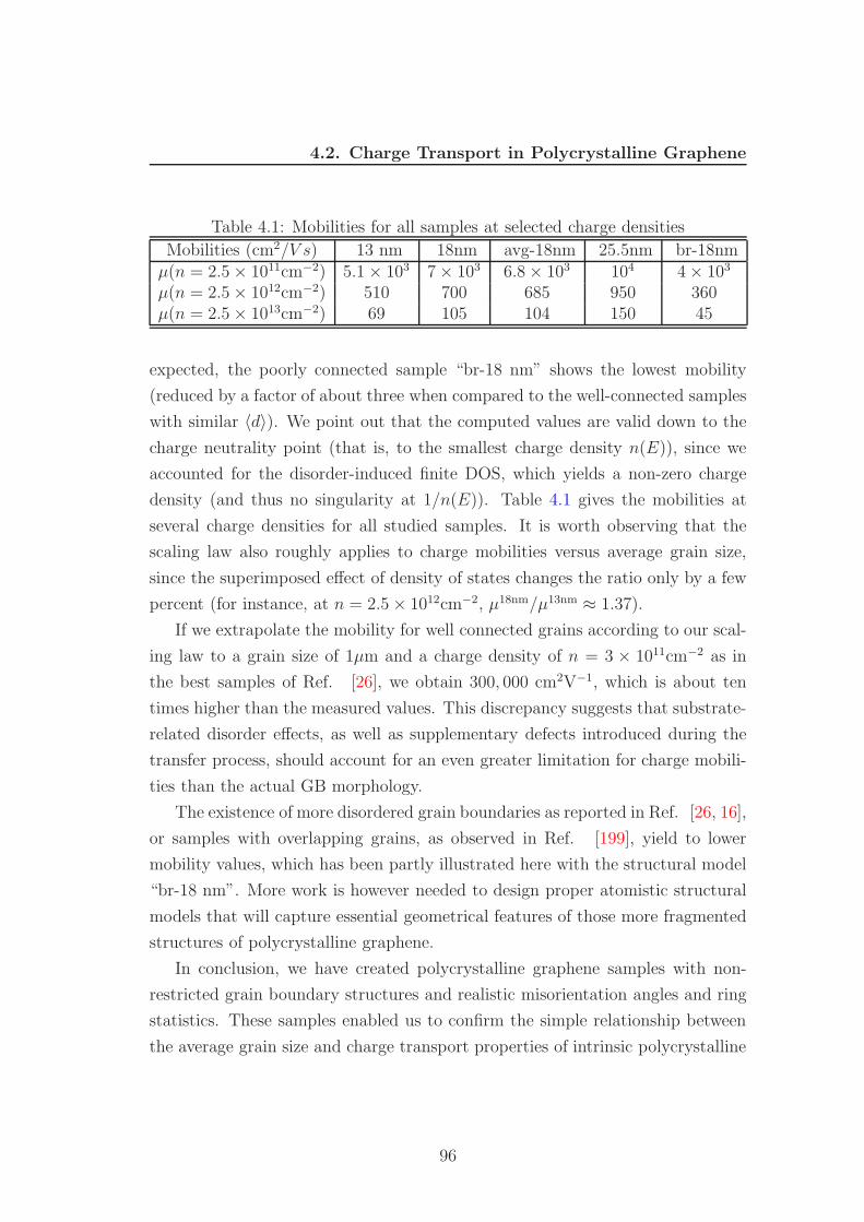
4.2. Charge Transport in Polycrystalline Graphene
Table 4.1: Mobilities for all samples at selected charge densities
Mobilities (cm2/V s) 13 nm 18nm avg-18nm 25.5nm br-18nmµ(n = 2.5 × 1011cm−2) 5.1 × 10³ 7 × 10³ 6.8 × 10³ 104 4 × 10³
µ(n = 2.5 × 1012cm−2) 510 700 685 950 360µ(n = 2.5 × 1013cm−2) 69 105 104 150 45
expected, the poorly connected sample “br-18 nm” shows the lowest mobility
(reduced by a factor of about three when compared to the well-connected samples
with similar 〈d〉). We point out that the computed values are valid down to the
charge neutrality point (that is, to the smallest charge density n(E)), since we
accounted for the disorder-induced finite DOS, which yields a non-zero charge
density (and thus no singularity at 1/n(E)). Table 4.1 gives the mobilities at
several charge densities for all studied samples. It is worth observing that the
scaling law also roughly applies to charge mobilities versus average grain size,
since the superimposed effect of density of states changes the ratio only by a few
percent (for instance, at n = 2.5 × 1012cm−2, µ18nm/µ13nm ≈ 1.37).
If we extrapolate the mobility for well connected grains according to our scal-
ing law to a grain size of 1µm and a charge density of n = 3 × 1011cm−2 as in
the best samples of Ref. [26], we obtain 300, 000 cm2V−1, which is about ten
times higher than the measured values. This discrepancy suggests that substrate-
related disorder effects, as well as supplementary defects introduced during the
transfer process, should account for an even greater limitation for charge mobili-
ties than the actual GB morphology.
The existence of more disordered grain boundaries as reported in Ref. [26, 16],
or samples with overlapping grains, as observed in Ref. [199], yield to lower
mobility values, which has been partly illustrated here with the structural model
“br-18 nm”. More work is however needed to design proper atomistic structural
models that will capture essential geometrical features of those more fragmented
structures of polycrystalline graphene.
In conclusion, we have created polycrystalline graphene samples with non-
restricted grain boundary structures and realistic misorientation angles and ring
statistics. These samples enabled us to confirm the simple relationship between
the average grain size and charge transport properties of intrinsic polycrystalline
96
4.2. Charge Transport in Polycrystalline Graphene
graphene. This scaling law will be explained more below in Section 4.2.5.3. The
disorder scattering strength in polycrystalline graphene was found to depend on
the atomic structure of GBs (inducing quasi-bound states at resonant energy) and
wavefunction mismatch between the grains, which generate strongly fluctuating,
but highly localized electron-hole density fluctuations along the interfaces between
grains. Our results significantly improve the present theoretical understanding
on the influence of the detailed morphology of polycrystalline materials to their
measurable electronic properties. They offer the possibility for estimating charge
mobilities in suspended CVD-graphene samples based on the average grain sizes
and quality of the GBs. Furthermore, they establish quantitative foundations
for estimating the intrinsic limits of charge transport in polycrystalline graphene,
which is of prime importance for graphene-based applications in the future.
4.2.5 Measurement of Electrical Transport across GGBs
Various measurements have been made to understand the electrical properties
of GGBs. These measurements fall into three primary approaches. The first ap-
proach involves local two-point measurements, which are accomplished with STM
and scanning tunneling spectroscopy (STS). [16, 200, 201, 202, 24, 23] With these
measurements, it is possible to deduce the local electronic density of states, the lo-
cal charge density, and the charge scattering mechanisms associated with GGBs,
thus permitting the spatially-dependent electrical characterization of GGBs at
the atomic scale. The second approach involves four-probe measurements, which
can be used to analyze the influence of individual GGBs at a scale of several mi-
crometers. [26, 181, 25] By subtracting the contribution of each graphene grain
from an inter-grain resistance measurement, the resistivity of a single GGB can be
estimated. In combination with microscopic or spectroscopic techniques, this ap-
proach allows one to correlate the resistivity of a single GGB with its structural
or chemical properties. Finally, the global impact of GGBs can be studied by
measuring the sheet resistance of polycrystalline graphene samples over a wide
range of average grain sizes and distributions, which are tunable by the CVD
growth conditions. By employing a simple scaling law (as discussed below), it is
then possible to extrapolate the average GB resistivity. [18, 27] Taken together,
97
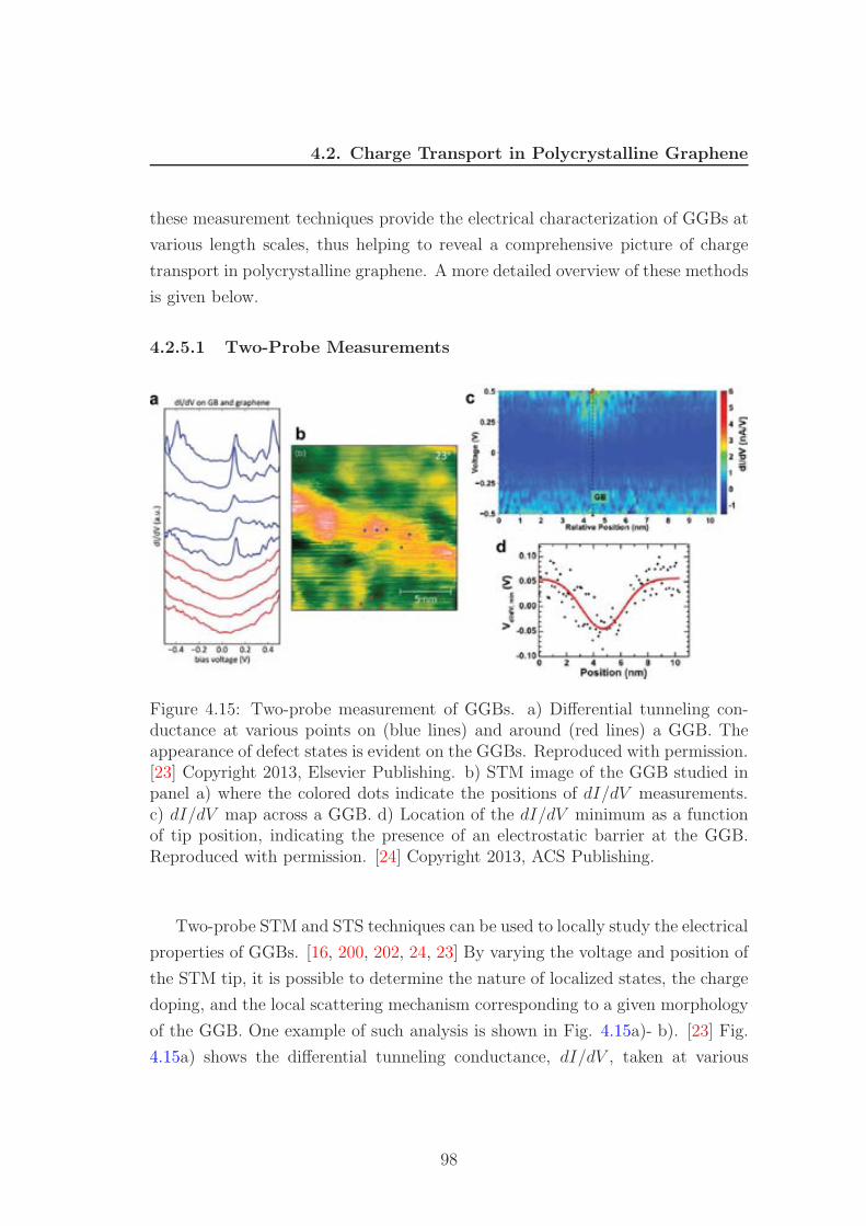
4.2. Charge Transport in Polycrystalline Graphene
these measurement techniques provide the electrical characterization of GGBs at
various length scales, thus helping to reveal a comprehensive picture of charge
transport in polycrystalline graphene. A more detailed overview of these methods
is given below.
4.2.5.1 Two-Probe Measurements
Figure 4.15: Two-probe measurement of GGBs. a) Differential tunneling con-ductance at various points on (blue lines) and around (red lines) a GGB. Theappearance of defect states is evident on the GGBs. Reproduced with permission.[23] Copyright 2013, Elsevier Publishing. b) STM image of the GGB studied inpanel a) where the colored dots indicate the positions of dI/dV measurements.c) dI/dV map across a GGB. d) Location of the dI/dV minimum as a functionof tip position, indicating the presence of an electrostatic barrier at the GGB.Reproduced with permission. [24] Copyright 2013, ACS Publishing.
Two-probe STM and STS techniques can be used to locally study the electrical
properties of GGBs. [16, 200, 202, 24, 23] By varying the voltage and position of
the STM tip, it is possible to determine the nature of localized states, the charge
doping, and the local scattering mechanism corresponding to a given morphology
of the GGB. One example of such analysis is shown in Fig. 4.15a)- b). [23] Fig.
4.15a) shows the differential tunneling conductance, dI/dV , taken at various
98
4.2. Charge Transport in Polycrystalline Graphene
points on (blue curves) and next to (red curves) a GGB in CVD-grown graphene.
A STM profile of the GGB and the points where the measurements were made
is shown in Fig. 4.15b). These results indicate the presence of a peak in the
tunneling conductance near the Dirac point whenever the STM tip lies on top of
the GGB. Meanwhile, this peak does not appear for measurements away from the
GGBs. Density functional theory (DFT) calculations have attributed this peak to
the localized states arising from two-coordinated carbon atoms in the GGBs. [23]
The STM map (not shown here) also reveals interference superstructures due to
scattering from the GGBs, indicating the contribution of significant inter-valley
scattering. This supports the hypothesis about the presence of two-coordinated
atoms, since inter-valley scattering stems from atomic-scale lattice defects. [131]
Fig. 4.15c) shows another map of dI/dV curves as the STM tip is scanned
across a GGB. [20] Similar to Fig. 4.15a), an enhanced local density of states is
observed at positive voltage when the tip is located over the GGB. The voltage
associated with the minimum of dI/dV , as shown in Fig. 4.15d), indicates a
strong negative shift around the position of the GGB, revealing n-type doping
of the GGB compared to bulk p-type doping of the graphene grains. This shift
in doping corresponds to an electrostatic potential barrier of a few tens of meV.
Finally, STM interference patterns indicate that some GGBs are dominated by
inter-valley scattering while others are dominated by backscattering. The type
of scattering appears to depend on the structure of the GGB, where a GGB
consisting of a continuous line of defects shows primarily backscattering behavior
and a periodic line of isolated defects is dominated by inter-valley scattering.
Other STM studies of GGBs reveal similar results to those mentioned above,
with GGBs forming p− n− p or p− p′ − p junctions with the bulk-like graphene
grains, where p′ < p. The doped regions associated with the GGBs are on the
order of a few nm wide, showing an abrupt transition between the GGB and
the grain. [16, 24] Other works reveal the presence of localized states along GBs
in graphene and graphite. [20, 200, 36] In general, STM/STS studies indicate
that GGBs are a source of localized states and electrostatic potential barriers in
polycrystalline graphene, and can serve as significant sources of charge scattering.
99
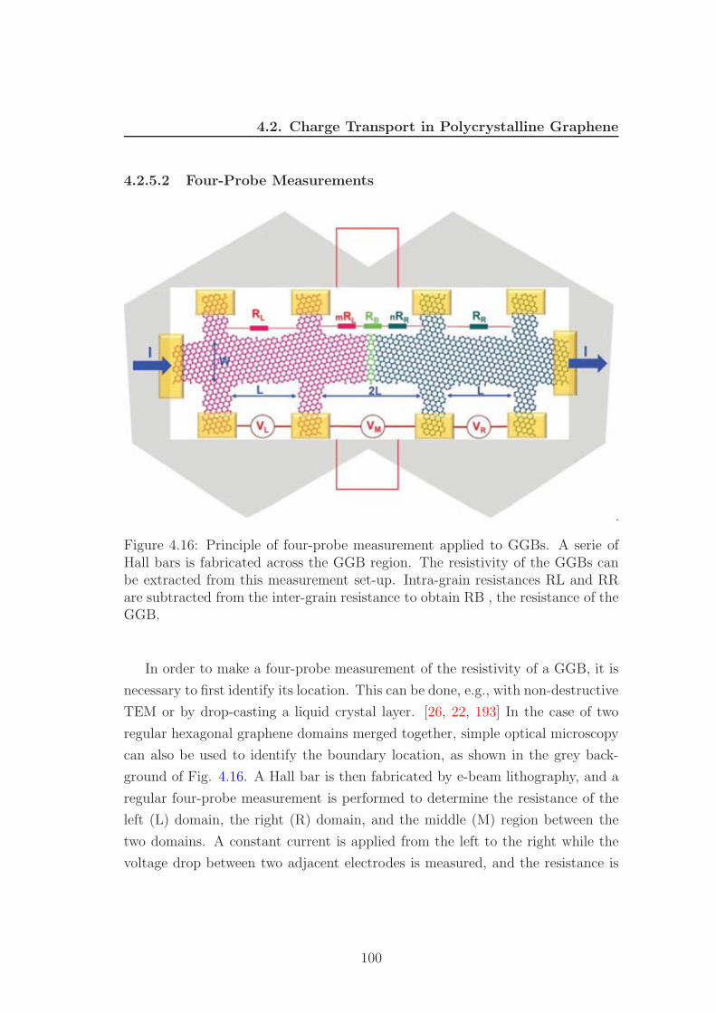
4.2. Charge Transport in Polycrystalline Graphene
4.2.5.2 Four-Probe Measurements
Figure 4.16: Principle of four-probe measurement applied to GGBs. A serie ofHall bars is fabricated across the GGB region. The resistivity of the GGBs canbe extracted from this measurement set-up. Intra-grain resistances RL and RRare subtracted from the inter-grain resistance to obtain RB , the resistance of theGGB.
In order to make a four-probe measurement of the resistivity of a GGB, it is
necessary to first identify its location. This can be done, e.g., with non-destructive
TEM or by drop-casting a liquid crystal layer. [26, 22, 193] In the case of two
regular hexagonal graphene domains merged together, simple optical microscopy
can also be used to identify the boundary location, as shown in the grey back-
ground of Fig. 4.16. A Hall bar is then fabricated by e-beam lithography, and a
regular four-probe measurement is performed to determine the resistance of the
left (L) domain, the right (R) domain, and the middle (M) region between the
two domains. A constant current is applied from the left to the right while the
voltage drop between two adjacent electrodes is measured, and the resistance is
100
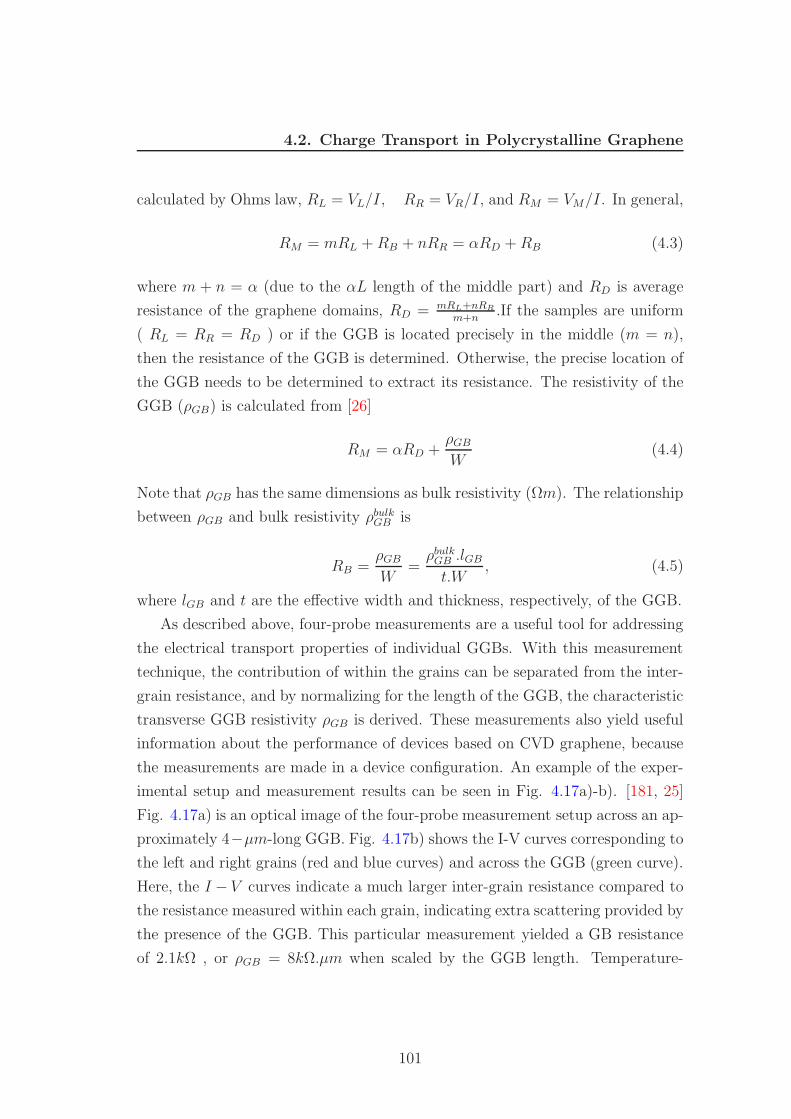
4.2. Charge Transport in Polycrystalline Graphene
calculated by Ohms law, RL = VL/I, RR = VR/I, and RM = VM/I. In general,
RM = mRL +RB + nRR = αRD +RB (4.3)
where m + n = α (due to the αL length of the middle part) and RD is average
resistance of the graphene domains, RD = mRL+nRR
m+n.If the samples are uniform
( RL = RR = RD ) or if the GGB is located precisely in the middle (m = n),
then the resistance of the GGB is determined. Otherwise, the precise location of
the GGB needs to be determined to extract its resistance. The resistivity of the
GGB (ρGB) is calculated from [26]
RM = αRD +ρGB
W(4.4)
Note that ρGB has the same dimensions as bulk resistivity (Ωm). The relationship
between ρGB and bulk resistivity ρbulkGB is
RB =ρGB
W=ρbulkGB .lGB
t.W, (4.5)
where lGB and t are the effective width and thickness, respectively, of the GGB.
As described above, four-probe measurements are a useful tool for addressing
the electrical transport properties of individual GGBs. With this measurement
technique, the contribution of within the grains can be separated from the inter-
grain resistance, and by normalizing for the length of the GGB, the characteristic
transverse GGB resistivity ρGB is derived. These measurements also yield useful
information about the performance of devices based on CVD graphene, because
the measurements are made in a device configuration. An example of the exper-
imental setup and measurement results can be seen in Fig. 4.17a)-b). [181, 25]
Fig. 4.17a) is an optical image of the four-probe measurement setup across an ap-
proximately 4−µm-long GGB. Fig. 4.17b) shows the I-V curves corresponding to
the left and right grains (red and blue curves) and across the GGB (green curve).
Here, the I − V curves indicate a much larger inter-grain resistance compared to
the resistance measured within each grain, indicating extra scattering provided by
the presence of the GGB. This particular measurement yielded a GB resistance
of 2.1kΩ , or ρGB = 8kΩ.µm when scaled by the GGB length. Temperature-
101
4.2. Charge Transport in Polycrystalline Graphene
Figure 4.17: Four-probe measurement of GGBs. a) Example of a four-probe setupfor measuring the resistivity of a GGB. b) I−V curves measured within individualgrains (red and blue curves) and across the GGB (green curve). The reducedslope for the inter-grain measurement indicates extra resistance contributed bythe GGB. Reproduced with permission. [25] Copyright 2011, Nature PublishingGroup. c) Four-probe measurement setup mounted on a TEM holder, whereindividual graphene grains are identified in the red and blue regions. d) Top plot;four-probe measurements of the inter- and intra-grain resistance as a function ofgate voltage (black and gray curves, respectively). Bottom plot; the extractedGB resistivity as a function of gate voltage in volt. Reproduced with permission.[26] Copyright 2013, AAAS.
102
4.2. Charge Transport in Polycrystalline Graphene
dependent measurements show that ρGB is insensitive to temperature, pointing
to a defect-induced scattering mechanism. Magnetotransport measurements re-
veal the presence of weak localization at low temperatures, [181, 25] indicating
that GGBs are significant sources of inter-valley scattering, in agreement with
the STM studies mentioned above.
A similar measurement setup is shown in Fig. 4.17c), on a device fabricated on
a specially prepared TEM window that allows for concurrent transport measure-
ments and identification of the individual grains and the GGB. [26] An example
of the measurement results can be seen in Fig. 4.17d). In the top graph, the gray
curves correspond to the resistance measured within each grain, while the black
curve is the inter-grain resistance. In the bottom graph, the green curve shows the
extracted GB resistivity as a function of applied gate voltage. Here, ρGB peaks at
a value of 4kΩ.µm at the Dirac point. With the four-probe measurements, ρGB
has been extracted for CVD graphene prepared under several growth conditions,
and it has been shown that the resistivity depends strongly on the structure
of the GGB. For example, a growth procedure yielding well-connected grains
gives ρGB = 1 to 4kΩ.µm at the Dirac point, while a growth procedure yielding
poorly-stitched grains results in values of ρGB an order of magnitude larger. In-
terestingly, some overlapping GBs have a negative resistivity, with the inter-grain
resistance smaller than the combined resistance of the individual grains. This is
attributed to reduced scattering in the double-layer overlapped region compared
to the single-layer grains.
4.2.5.3 Global Measurements from Scaling Law
In general, GGBs are formed randomly during the CVD growth process, and
their electrical properties are not uniform. Therefore, in addition to studies of
individual GGBs, it is also necessary to study GGBs on a large scale to extract a
reliable average of their transport properties. This average quantity is represented
by the GB resistivity DG B , which can be extracted from an Ohmic scaling
law, as illustrated in Fig. 4.18. Fig. 4.18a) shows a 1D model of n graphene
grains separated by n GBs. The sample resistance R includes the resistance
of the n grains RGi , and the resistance of the n GGBs RGB
i (R =∑n
i=1RGi +
103
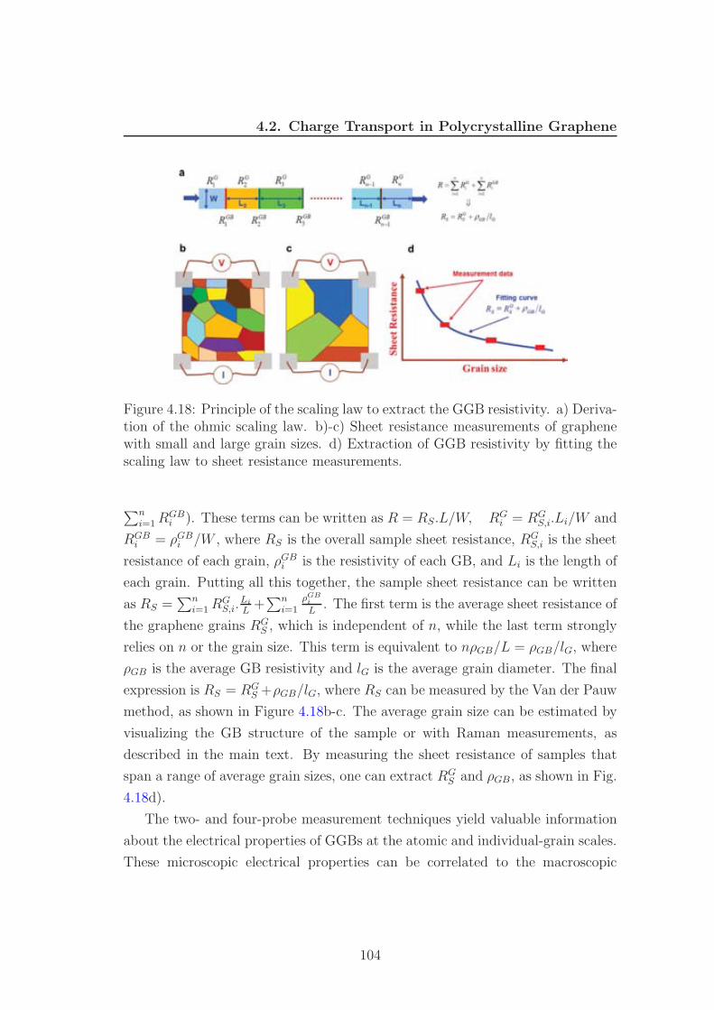
4.2. Charge Transport in Polycrystalline Graphene
Figure 4.18: Principle of the scaling law to extract the GGB resistivity. a) Deriva-tion of the ohmic scaling law. b)-c) Sheet resistance measurements of graphenewith small and large grain sizes. d) Extraction of GGB resistivity by fitting thescaling law to sheet resistance measurements.
∑ni=1R
GBi ). These terms can be written as R = RS.L/W, RG
i = RGS,i.Li/W and
RGBi = ρGB
i /W , where RS is the overall sample sheet resistance, RGS,i is the sheet
resistance of each grain, ρGBi is the resistivity of each GB, and Li is the length of
each grain. Putting all this together, the sample sheet resistance can be written
as RS =∑n
i=1RGS,i.
Li
L+∑n
i=1ρGBi
L. The first term is the average sheet resistance of
the graphene grains RGS , which is independent of n, while the last term strongly
relies on n or the grain size. This term is equivalent to nρGB/L = ρGB/lG, where
ρGB is the average GB resistivity and lG is the average grain diameter. The final
expression is RS = RGS +ρGB/lG, where RS can be measured by the Van der Pauw
method, as shown in Figure 4.18b-c. The average grain size can be estimated by
visualizing the GB structure of the sample or with Raman measurements, as
described in the main text. By measuring the sheet resistance of samples that
span a range of average grain sizes, one can extract RGS and ρGB, as shown in Fig.
4.18d).
The two- and four-probe measurement techniques yield valuable information
about the electrical properties of GGBs at the atomic and individual-grain scales.
These microscopic electrical properties can be correlated to the macroscopic
104
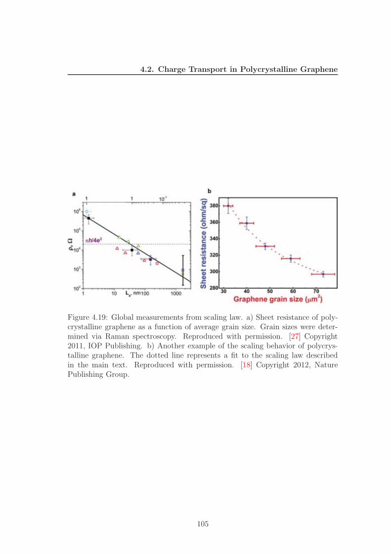
4.2. Charge Transport in Polycrystalline Graphene
Figure 4.19: Global measurements from scaling law. a) Sheet resistance of poly-crystalline graphene as a function of average grain size. Grain sizes were deter-mined via Raman spectroscopy. Reproduced with permission. [27] Copyright2011, IOP Publishing. b) Another example of the scaling behavior of polycrys-talline graphene. The dotted line represents a fit to the scaling law describedin the main text. Reproduced with permission. [18] Copyright 2012, NaturePublishing Group.
105
4.2. Charge Transport in Polycrystalline Graphene
ones, which are applicable to the analysis of experimentally available large-area
graphene. This can be accomplished with the global scaling law, as discussed
above. Two examples of this procedure are given in Fig. 4.19a)-b). Fig. 4.19a)
shows a series of sheet resistance measurements over several orders of magnitude
of average grain size. [27, 131, 203, 204, 205, 206] Applying the scaling law to this
data (black line in Fig. 4.19a) results in ρGB = 0.67kΩ.µm. This value is some-
what lower than those obtained in the fourprobe measurements mentioned above.
However, because the measurements did not involve back gate modulation, it is
likely that the sheet resistance was measured away from the Dirac point, resulting
in a lower value of ρGB . It should also be noted that the x-axis of Fig. 4.19a)
was obtained through the D/G ratio in Raman spectroscopy, and thus represents
an average distance between defects rather than the true grain size.
Another example of the scaling behavior is shown in Figure 4.19b. [18] In
this case, the grain sizes are estimated with an optical microscope, and a fit to
the scaling law gives RGS = 130Ω and ρGB = 1.4kΩ.µm. One useful consequence
of using the scaling law is that it allows for an estimate of the average sheet
resistance within the grains, RDS (for a good fit, it is best to have a range of
grain sizes such that RGS < ρGB/lG for the smallest grains and RG
S > ρGB/lG
for the largest grains). For example, based on the extracted values of RGS and
ρGB , the GGBs begin to dominate the sheet resistance of these samples when
the average grain size is less than lG = ρGB/RGS ≈ 10µm. This information can
serve as a useful design parameter when considering large-scale applications of
polycrystalline graphene.
4.2.6 Manipulation of GGBs with Functional Groups
4.2.6.1 Chemical Reactivity of GGBs
In addition to the general electrical transport properties of polycrystalline graphene,
the chemical properties (reactivity, functionalization, etc.) of GGBs have been
extensively discussed. For example, it has been shown theoretically that non-
hexagonal atomic arrangements in graphene, such as the Stone-Wales defect,
yield higher chemical reactivity than the ideal hexagonal structure, [80, 207, 208,
209, 210] and this behavior has been extended to GGBs. A schematic represen-
106
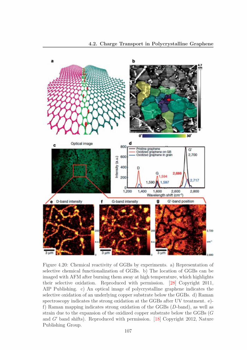
4.2. Charge Transport in Polycrystalline Graphene
Figure 4.20: Chemical reactivity of GGBs by experiments. a) Representation ofselective chemical functionalization of GGBs. b) The location of GGBs can beimaged with AFM after burning them away at high temperature, which highlightstheir selective oxidation. Reproduced with permission. [28] Copyright 2011,AIP Publishing. c) An optical image of polycrystalline graphene indicates theselective oxidation of an underlying copper substrate below the GGBs. d) Ramanspectroscopy indicates the strong oxidation at the GGBs after UV treatment. e)-f) Raman mapping indicates strong oxidation of the GGBs (D-band), as well asstrain due to the expansion of the oxidized copper substrate below the GGBs (Gand G′ band shifts). Reproduced with permission. [18] Copyright 2012, NaturePublishing Group.
107
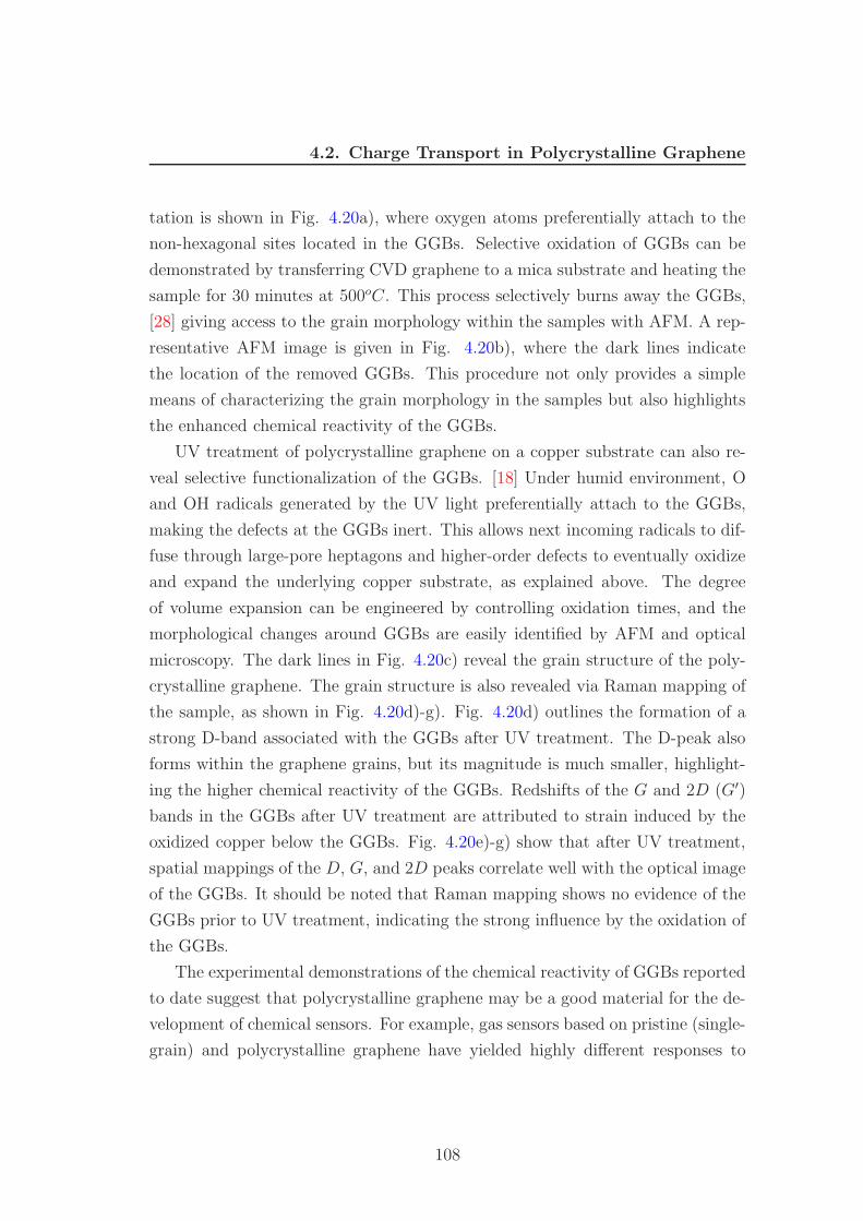
4.2. Charge Transport in Polycrystalline Graphene
tation is shown in Fig. 4.20a), where oxygen atoms preferentially attach to the
non-hexagonal sites located in the GGBs. Selective oxidation of GGBs can be
demonstrated by transferring CVD graphene to a mica substrate and heating the
sample for 30 minutes at 500oC. This process selectively burns away the GGBs,
[28] giving access to the grain morphology within the samples with AFM. A rep-
resentative AFM image is given in Fig. 4.20b), where the dark lines indicate
the location of the removed GGBs. This procedure not only provides a simple
means of characterizing the grain morphology in the samples but also highlights
the enhanced chemical reactivity of the GGBs.
UV treatment of polycrystalline graphene on a copper substrate can also re-
veal selective functionalization of the GGBs. [18] Under humid environment, O
and OH radicals generated by the UV light preferentially attach to the GGBs,
making the defects at the GGBs inert. This allows next incoming radicals to dif-
fuse through large-pore heptagons and higher-order defects to eventually oxidize
and expand the underlying copper substrate, as explained above. The degree
of volume expansion can be engineered by controlling oxidation times, and the
morphological changes around GGBs are easily identified by AFM and optical
microscopy. The dark lines in Fig. 4.20c) reveal the grain structure of the poly-
crystalline graphene. The grain structure is also revealed via Raman mapping of
the sample, as shown in Fig. 4.20d)-g). Fig. 4.20d) outlines the formation of a
strong D-band associated with the GGBs after UV treatment. The D-peak also
forms within the graphene grains, but its magnitude is much smaller, highlight-
ing the higher chemical reactivity of the GGBs. Redshifts of the G and 2D (G′)
bands in the GGBs after UV treatment are attributed to strain induced by the
oxidized copper below the GGBs. Fig. 4.20e)-g) show that after UV treatment,
spatial mappings of the D, G, and 2D peaks correlate well with the optical image
of the GGBs. It should be noted that Raman mapping shows no evidence of the
GGBs prior to UV treatment, indicating the strong influence by the oxidation of
the GGBs.
The experimental demonstrations of the chemical reactivity of GGBs reported
to date suggest that polycrystalline graphene may be a good material for the de-
velopment of chemical sensors. For example, gas sensors based on pristine (single-
grain) and polycrystalline graphene have yielded highly different responses to
108
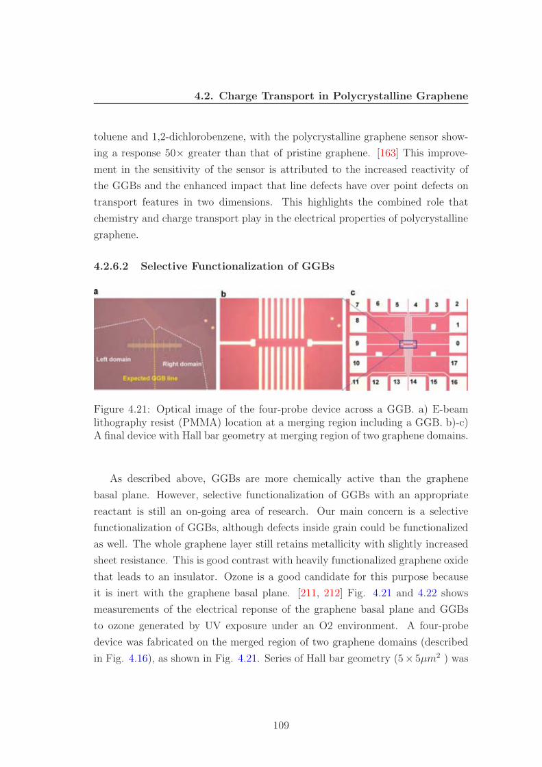
4.2. Charge Transport in Polycrystalline Graphene
toluene and 1,2-dichlorobenzene, with the polycrystalline graphene sensor show-
ing a response 50× greater than that of pristine graphene. [163] This improve-
ment in the sensitivity of the sensor is attributed to the increased reactivity of
the GGBs and the enhanced impact that line defects have over point defects on
transport features in two dimensions. This highlights the combined role that
chemistry and charge transport play in the electrical properties of polycrystalline
graphene.
4.2.6.2 Selective Functionalization of GGBs
Figure 4.21: Optical image of the four-probe device across a GGB. a) E-beamlithography resist (PMMA) location at a merging region including a GGB. b)-c)A final device with Hall bar geometry at merging region of two graphene domains.
As described above, GGBs are more chemically active than the graphene
basal plane. However, selective functionalization of GGBs with an appropriate
reactant is still an on-going area of research. Our main concern is a selective
functionalization of GGBs, although defects inside grain could be functionalized
as well. The whole graphene layer still retains metallicity with slightly increased
sheet resistance. This is good contrast with heavily functionalized graphene oxide
that leads to an insulator. Ozone is a good candidate for this purpose because
it is inert with the graphene basal plane. [211, 212] Fig. 4.21 and 4.22 shows
measurements of the electrical reponse of the graphene basal plane and GGBs
to ozone generated by UV exposure under an O2 environment. A four-probe
device was fabricated on the merged region of two graphene domains (described
in Fig. 4.16), as shown in Fig. 4.21. Series of Hall bar geometry (5× 5µm2 ) was
109
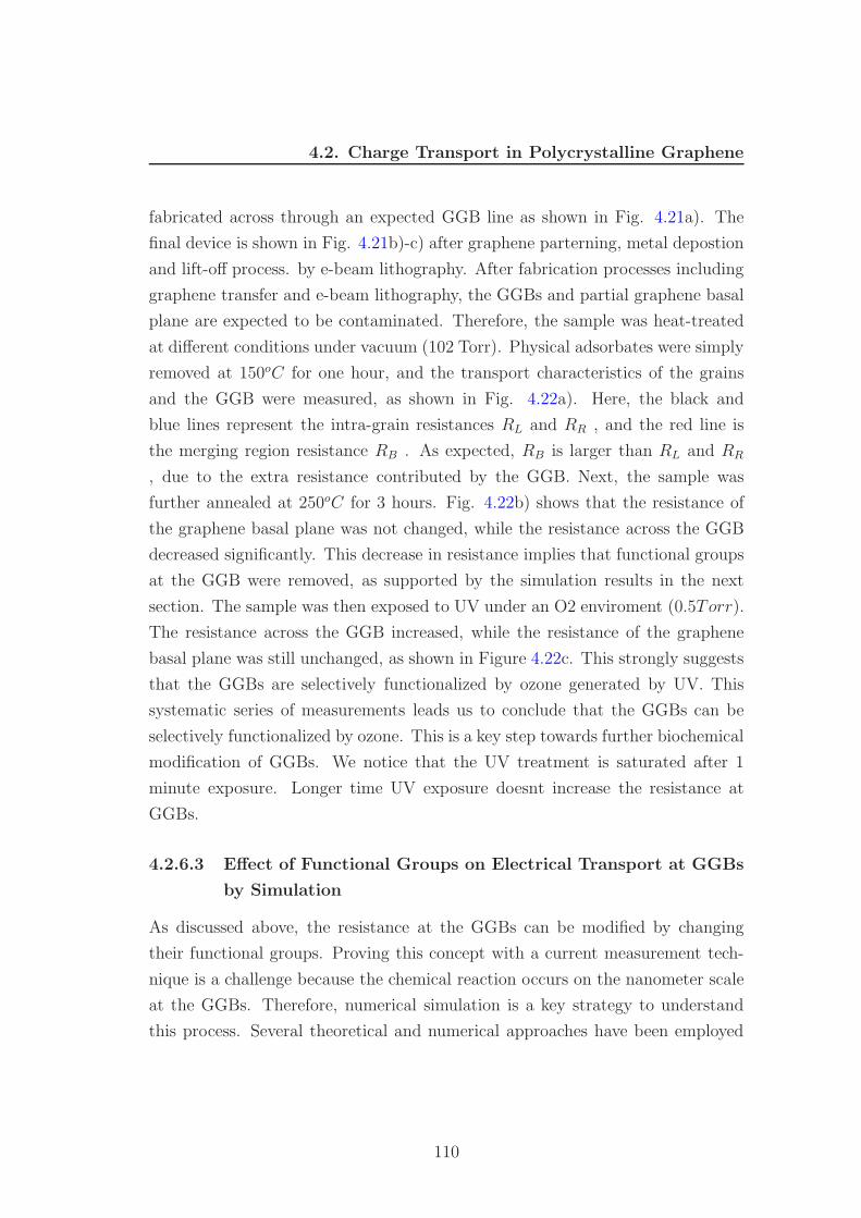
4.2. Charge Transport in Polycrystalline Graphene
fabricated across through an expected GGB line as shown in Fig. 4.21a). The
final device is shown in Fig. 4.21b)-c) after graphene parterning, metal depostion
and lift-off process. by e-beam lithography. After fabrication processes including
graphene transfer and e-beam lithography, the GGBs and partial graphene basal
plane are expected to be contaminated. Therefore, the sample was heat-treated
at different conditions under vacuum (102 Torr). Physical adsorbates were simply
removed at 150oC for one hour, and the transport characteristics of the grains
and the GGB were measured, as shown in Fig. 4.22a). Here, the black and
blue lines represent the intra-grain resistances RL and RR , and the red line is
the merging region resistance RB . As expected, RB is larger than RL and RR
, due to the extra resistance contributed by the GGB. Next, the sample was
further annealed at 250oC for 3 hours. Fig. 4.22b) shows that the resistance of
the graphene basal plane was not changed, while the resistance across the GGB
decreased significantly. This decrease in resistance implies that functional groups
at the GGB were removed, as supported by the simulation results in the next
section. The sample was then exposed to UV under an O2 enviroment (0.5Torr).
The resistance across the GGB increased, while the resistance of the graphene
basal plane was still unchanged, as shown in Figure 4.22c. This strongly suggests
that the GGBs are selectively functionalized by ozone generated by UV. This
systematic series of measurements leads us to conclude that the GGBs can be
selectively functionalized by ozone. This is a key step towards further biochemical
modification of GGBs. We notice that the UV treatment is saturated after 1
minute exposure. Longer time UV exposure doesnt increase the resistance at
GGBs.
4.2.6.3 Effect of Functional Groups on Electrical Transport at GGBs
by Simulation
As discussed above, the resistance at the GGBs can be modified by changing
their functional groups. Proving this concept with a current measurement tech-
nique is a challenge because the chemical reaction occurs on the nanometer scale
at the GGBs. Therefore, numerical simulation is a key strategy to understand
this process. Several theoretical and numerical approaches have been employed
110
4.2. Charge Transport in Polycrystalline Graphene
Figure 4.22: O2 Selective functionalization of GGBs by UV treatment underenvironment.a)-b) Effect of annealing at 250oC in 3h. Funtional groups are re-moved from a GGB. c)-d) Effect of UV treatment under O2 environment. Theexclusive change of the inter-grain resistance indicates selective functionalizationat the GGB. The UV treatment is saturated after 1 minute of UV treatment.
111
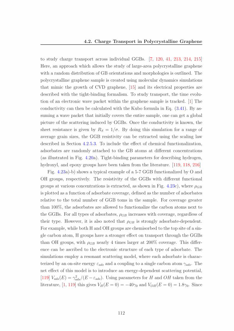
4.2. Charge Transport in Polycrystalline Graphene
to study charge transport across individual GGBs. [7, 120, 41, 213, 214, 215]
Here, an approach which allows the study of large-area polycrystalline graphene
with a random distribution of GB orientations and morphologies is outlined. The
polycrystalline graphene sample is created using molecular dynamics simulations
that mimic the growth of CVD graphene, [15] and its electrical properties are
described with the tight-binding formalism. To study transport, the time evolu-
tion of an electronic wave packet within the graphene sample is tracked. [1] The
conductivity can then be calculated with the Kubo formula in Eq. (3.41). By as-
suming a wave packet that initially covers the entire sample, one can get a global
picture of the scattering induced by GGBs. Once the conductivity is known, the
sheet resistance is given by RS = 1/σ. By doing this simulation for a range of
average grain sizes, the GGB resistivity can be extracted using the scaling law
described in Section 4.2.5.3. To include the effect of chemical functionalization,
adsorbates are randomly attached to the GB atoms at different concentrations
(as illustrated in Fig. 4.20a). Tight-binding parameters for describing hydrogen,
hydroxyl, and epoxy groups have been taken from the literature. [119, 118, 216]
Fig. 4.23a)-b) shows a typical example of a 5-7 GGB functionalized by O and
OH groups, respectively. The resistivity of the GGBs with different functional
groups at various concentrations is extracted, as shown in Fig. 4.23c), where ρGB
is plotted as a function of adsorbate coverage, defined as the number of adsorbates
relative to the total number of GGB toms in the sample. For coverage greater
than 100%, the adsorbates are allowed to functionalize the carbon atoms next to
the GGBs. For all types of adsorbates, ρGB increases with coverage, regardless of
their type. However, it is also noted that ρGB is strongly adsorbate-dependent.
For example, while both H and OH groups are chemisorbed to the top site of a sin-
gle carbon atom, H groups have a stronger effect on transport through the GGBs
than OH groups, with ρGB nearly 4 times larger at 200% coverage. This differ-
ence can be ascribed to the electronic structure of each type of adsorbate. The
simulations employ a resonant scattering model, where each adsorbate is charac-
terized by an on-site energy εads and a coupling to a single carbon atom γads. The
net effect of this model is to introduce an energy-dependent scattering potential,
[119] Vads(E) = γ2ads/(E− εads). Using parameters for H and OH taken from the
literature, [1, 119] this gives VH(E = 0) = −40γ0 and VOH(E = 0) = 1.8γ0. Since
112
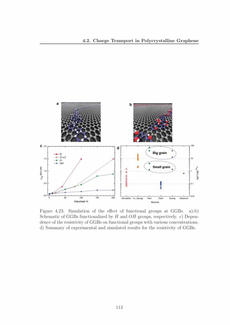
4.2. Charge Transport in Polycrystalline Graphene
Figure 4.23: Simulation of the effect of functional groups at GGBs. a)-b)Schematic of GGBs functionalized by H and OH groups, respectively. c) Depen-dence of the resistivity of GGBs on functional groups with various concentrations.d) Summary of experimental and simulated results for the resistivity of GGBs.
113
4.2. Charge Transport in Polycrystalline Graphene
σDC , and hence RS and ρGB , are calculated at the Dirac point, the H groups
present a much stronger scattering potential than the OH groups. Calculations
have also shown that H groups induce strongly localized states near the Dirac
point, while OH adsorbates result in a more dispersive impurity band lying in
the valence band of graphene. [119] Meanwhile, the O group chemisorbs in the
bridge site by forming a pair with adjacent carbon atoms in the graphene lattice
(epoxide). [216] The simulations clearly show that the resistance at GGBs with
functional groups is much higher than that of pure GGBs. Fig. 4.23d) shows a
summary of the values of ρGB derived from measurements compared to the simu-
lation results. [17, 180, 26, 120, 23, 216] The solid symbols are from the electrical
measurements described earlier In this section, and the open symbols are the nu-
merical simulations. Here, most measurements give ρGB in the range of 1 to 10
kΩ.µm, except for one that gives values one to two orders of magnitude smaller.
[79] This difference could be caused by the measurement technique, where ρGB
was measured with four-probe STM under ultra-high vacuum, while the other
groups fabricated physical contacts on their samples. This extra fabrication step
could lead to additional contamination, increasing ρGB . Accordingly, the numer-
ical simulations show that it is possible to bridge the gap between the various
measurements by systematically increasing the amount of chemical functional-
ization of the GGBs. The situation becomes more complicated by several other
parameters such as the structure and resistivity of the GGBs, as mentioned pre-
viously. [120] This is highlighted by the measurements labeled ”small grain” and
”large grain” in Fig. 4.23d), where growth conditions yielding large grain samples
also tend to yield poorly connected and highly resistive GGBs. [26] Nevertheless,
these results highlight the strong impact that chemical functionalization can have
on the electrical properties of GGBs.
4.2.7 Challenges and Opportunities
The observation and characterization of GGBs at both atomic and macroscopic
scale is mandatory to understand the transport properties and the related un-
derlying physics and chemistry of polycrystalline graphene. As described in this
Chapter, TEM and STM, combined with theory and simulation, can provide in-
114
4.2. Charge Transport in Polycrystalline Graphene
formation at the atomic scale, with the related transport properties revealed with
the assistance of STS. UV-treatment and liquid crystal coating, combined with
optical microscopy, can provide information on both the grain boundary distri-
bution at the macro scale and the orientation of each domain, while macroscopic
transport properties can be derived using the scaling law. With all these pow-
erful methods available, one can envision their application to the engineering of
grain boundaries during graphene synthesis. For instance, ideal monocrystalline
graphene could be obtained by designing seamless boundaries between coalesc-
ing graphene grains. With available large-area monocrystalline graphene, bilayer
graphene with controlled stacking order can be constructed by aligned transfer
techniques. The relative orientation of the layers can be identified by either low-
energy electron diffraction or Raman spectroscopy. This opens a new research
direction of bilayer graphene for designing vertical tunneling devices and planar
switching devices.
A grain boundary line is a 1D structure consisting of a series of pentagonal,
hexagonal, and heptagonal carbon rings. It is possible to selectively functionalize
as well as deposit designed materials only at the GGBs due to their higher chem-
ical reactivity compared to ideal basal graphene. This implies that GGBs can
be a good template for the synthesis of 1D materials. Atomic layer deposition,
whose precursor is quite inert with the graphene basal plane, would be a good
method for the synthesis of sub-nanometer 1D metals and semiconductors.
Another research direction to utilize grain boundaries is to control their den-
sity to design sensors for detecting gases and molecules under different environ-
mental conditions. As revealed by our numerical simulations and our experimen-
tal measurements, the transport properties of grain boundaries can be strongly
altered with chemical modifications of the grain boundaries. Together with highly
conductive graphene, electro-biochemical sensing devices with high sensitivity and
selectivity could be designed.
Membrane science is another open research area. Although the ideal hexago-
nal graphene lattice impedes the diffusion of gases, defect sites such as heptagons,
octagons, vacancies, and divacancies allow selective diffusion of limited gases and
molecules, as mentioned above. This provides new opportunities to explore ul-
trafine membrane performance via the controlled engineering of grain boundaries
115
4.3. Impact of Graphene Polycrystallinity on The Performance ...
and point defects.
Although much progress has been made in the visualization and electrical
characterization of GGBs from atomic scale to macro scale, issues still remain.
The structure of GGBs is determined by the different orientations between merg-
ing domains, and the related physical and chemical properties are predicted to be
strongly chirality-dependent. However, no electrical measurements have revealed
such effects. The question is whether this originates from a device fabrication
process which inevitably functionalizes GGBs, or if the native structure of GGBs
is disordered, different from theoretical predictions.
GGBs also present challenges for the development of large scale graphene-
based spintronic devices, [217] and for harvesting the unique optical properties
of graphene. For instance, GGBs introduce non-trivial local symmetry breaking
which could significantly impact spin/pseudospin coupling and spin relaxation
times, as well as the formation and propagation of plasmonic excitations. Simi-
larly, the peculiar structure of interconnected GGBs could affect transport prop-
erties in high magnetic fields, such as the quantum Hall effect. Overall, controlling
the atomic structure of GGBs by CVD is a big challenge from a scientific point
of view, but would be a huge step forward in the realization of next-generation
technologies based on this material.
4.3 Impact of Graphene Polycrystallinity on The
Performance of Graphene Field-effect Tran-
sistors
4.3.1 Introduction
In the effort to successfully realize next-generation technologies based on graphene
field-effect transistors (GFETs), theory and device modeling will play a crucial
role. Specifically, it is important to develop models that can accurately describe
both the electrostatics and the current-voltage ( I-V) characteristics of graphene-
based electronic devices. [218, 219, 220, 221] This capability will enable device
design optimization and performance projections, will permit benchmarking of
116
4.3. Impact of Graphene Polycrystallinity on The Performance ...
graphene-based technology against existing ones, [145, 222] and will help to ex-
plore the feasibility of analog/RF circuits based on graphene. [223, 224, 225]
Ultimately, graphene-based devices could provide new or improved functional-
ity with respect to existing technologies, such as those based on silicon or III-V
materials.
The chemical vapor deposition (CVD) technique for growing wafer-scale graphene
on metallic substrates [30, 31, 32, 33] produces a polycrystalline pattern. This
is because the growth of graphene is simultaneously initiated at different nucle-
ation sites, leading to samples with randomly distributed grains of varying lattice
orientations. [14] It has recently been predicted that the electronic properties of
polycrystalline graphene differ from those of pristine graphene (PG), where the
mobility scales linearly with the average grain size. [120] Based on these results,
we report on how the electronic properties of polycrystalline graphene (Poly-G)
impact the behavior of graphene-based devices. Specifically, we concentrate our
study on the effect that Poly-G has on the gate electrostatics and I-V character-
istics of GFETs. We find that the source-drain current and the transconductance
are proportional to the average grain size, indicating that these quantities are
hampered by the presence of grain boundaries (GBs) in the Poly-G. However,
our simulations also show that current saturation is improved by the presence of
GBs, and the intrinsic gain is insensitive to the grain size. These results indicate
that GBs play a complex role in the behavior of graphene-based electronics, and
their importance depends on the application of the device.
4.3.2 Poly-G Effect on the Gate Electrostatics and I-V
Characteristics of GFETs
The starting point of our study is the characterization of a large-area model
of disordered Poly-G samples, containing hundreds of thousands atoms and de-
scribed by varying grain misorientation angles, realistic carbon ring statistics,
and unrestricted GB structures, based on the method reported in Ref. [39] .
To calculate the electronic and transport properties, we used a tight-binding
(TB) Hamiltonian and an efficient quantum transport method, [136, 4] which is
particularly well-suited for large samples of disordered low-dimensional systems.
117
4.3. Impact of Graphene Polycrystallinity on The Performance ...
The transport calculations were based on a real-space order-N quantum wave
packet evolution approach, which allowed us to compute the Kubo-Greenwood
conductivity (Eq. (3.41)). With this quantity, the charge carrier mobility can be
estimated as µ(E) = σ(E)/q∗Qc(E), where Qc is the 2D charge density in the
graphene. It should be noted that we assume the carrier mobility is not limited
by the substrate, that is, we do not consider additional scattering due to charge
traps or surface phonons in the insulator that could further degrade the carrier
mobility. [226] Thus, our results represent an upper bound on the performance
metrics of the GFETs that we are studying.
In this work, we focus on a dual-gate GFET as the one depicted in Fig. 4.24 .
This transistor is based on a metal/oxide/Poly-G/oxide/semiconductor structure
where an external electric field modulates the mobile carrier density in the Poly-G
layer. The electrostatics of this dual gate structure can be understood with an
application of Gauss law
Qc = Ct(V∗gs − Vc) + Cb(V
∗bs − Vc) (4.6)
where Qc = q(p − n) is the net mobile charge density in the graphene channel,
Ct and Cb are the geometrical top and bottom oxide capacitances, and V ∗gs and
V ∗bs are the effective top and bottom gate-source voltages, respectively. Here,
V ∗gs = Vgs−Vgs0 and V ∗
bs = Vbs−Vbs0, where Vgs0 and Vbs0 are quantities that com-
prise the work function differences between each gate and the graphene channel,
charged interface states at the graphene/oxide interfaces, and possible doping of
the graphene. The graphene charge density can be determined numerically using
the procedure
Qc(Vc) = q
∫ 0
−∞
DOSp−G(E)f(qVc − E)dE − q
∫ ∞
0
DOSp−G(E)f(E − qVc)dE
(4.7)
where DOSp−G(E) has been calculated with the procedure outlined in Ref. [120].
The potential Vc represents the voltage drop across the graphene layer, and is
related to the quantum capacitance Cq of the Poly-G by Cq = −dQc/dVc . When
the entire length of the transistor is considered, the effective gate voltages can be
written as V ∗gs = Vgs − Vgs0 − V (x) and V ∗
bs = Vbs − Vbs0 − V (x), where V (x) (the
118
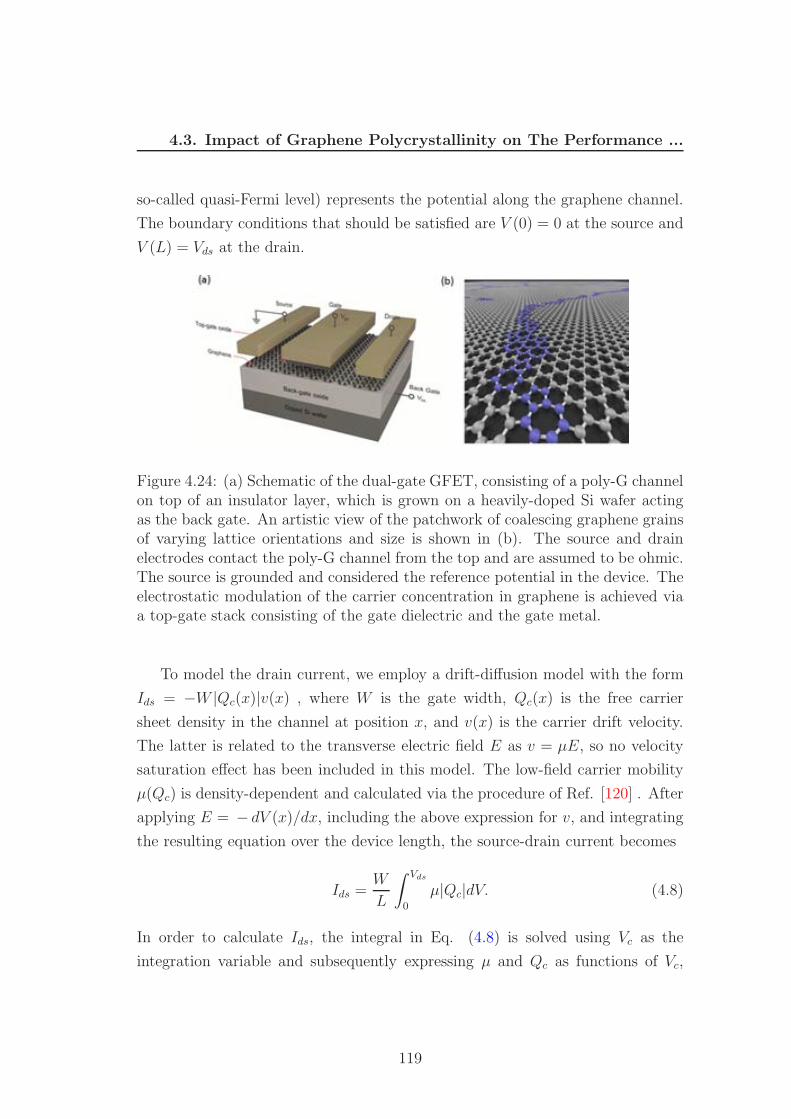
4.3. Impact of Graphene Polycrystallinity on The Performance ...
so-called quasi-Fermi level) represents the potential along the graphene channel.
The boundary conditions that should be satisfied are V (0) = 0 at the source and
V (L) = Vds at the drain.
Figure 4.24: (a) Schematic of the dual-gate GFET, consisting of a poly-G channelon top of an insulator layer, which is grown on a heavily-doped Si wafer actingas the back gate. An artistic view of the patchwork of coalescing graphene grainsof varying lattice orientations and size is shown in (b). The source and drainelectrodes contact the poly-G channel from the top and are assumed to be ohmic.The source is grounded and considered the reference potential in the device. Theelectrostatic modulation of the carrier concentration in graphene is achieved viaa top-gate stack consisting of the gate dielectric and the gate metal.
To model the drain current, we employ a drift-diffusion model with the form
Ids = −W |Qc(x)|v(x) , where W is the gate width, Qc(x) is the free carrier
sheet density in the channel at position x, and v(x) is the carrier drift velocity.
The latter is related to the transverse electric field E as v = µE, so no velocity
saturation effect has been included in this model. The low-field carrier mobility
µ(Qc) is density-dependent and calculated via the procedure of Ref. [120] . After
applying E = − dV (x)/dx, including the above expression for v, and integrating
the resulting equation over the device length, the source-drain current becomes
Ids =W
L
∫ Vds
0
µ|Qc|dV. (4.8)
In order to calculate Ids, the integral in Eq. (4.8) is solved using Vc as the
integration variable and subsequently expressing µ and Qc as functions of Vc,
119
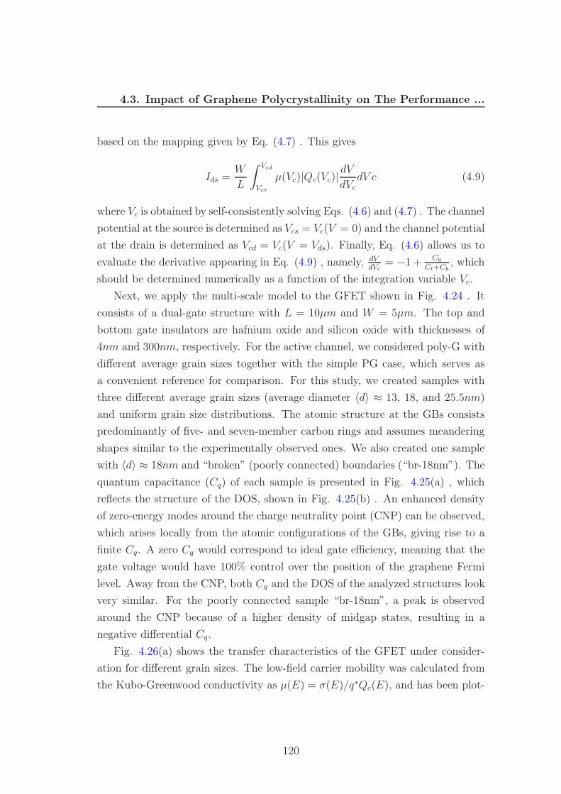
4.3. Impact of Graphene Polycrystallinity on The Performance ...
based on the mapping given by Eq. (4.7) . This gives
Ids =W
L
∫ Vcd
Vcs
µ(Vc)|Qc(Vc)|dV
dVcdV c (4.9)
where Vc is obtained by self-consistently solving Eqs. (4.6) and (4.7) . The channel
potential at the source is determined as Vcs = Vc(V = 0) and the channel potential
at the drain is determined as Vcd = Vc(V = Vds). Finally, Eq. (4.6) allows us to
evaluate the derivative appearing in Eq. (4.9) , namely, dVdVc
= −1 + Cq
Ct+Cb, which
should be determined numerically as a function of the integration variable Vc.
Next, we apply the multi-scale model to the GFET shown in Fig. 4.24 . It
consists of a dual-gate structure with L = 10µm and W = 5µm. The top and
bottom gate insulators are hafnium oxide and silicon oxide with thicknesses of
4nm and 300nm, respectively. For the active channel, we considered poly-G with
different average grain sizes together with the simple PG case, which serves as
a convenient reference for comparison. For this study, we created samples with
three different average grain sizes (average diameter 〈d〉 ≈ 13, 18, and 25.5nm)
and uniform grain size distributions. The atomic structure at the GBs consists
predominantly of five- and seven-member carbon rings and assumes meandering
shapes similar to the experimentally observed ones. We also created one sample
with 〈d〉 ≈ 18nm and “broken” (poorly connected) boundaries (“br-18nm”). The
quantum capacitance (Cq) of each sample is presented in Fig. 4.25(a) , which
reflects the structure of the DOS, shown in Fig. 4.25(b) . An enhanced density
of zero-energy modes around the charge neutrality point (CNP) can be observed,
which arises locally from the atomic configurations of the GBs, giving rise to a
finite Cq. A zero Cq would correspond to ideal gate efficiency, meaning that the
gate voltage would have 100% control over the position of the graphene Fermi
level. Away from the CNP, both Cq and the DOS of the analyzed structures look
very similar. For the poorly connected sample “br-18nm”, a peak is observed
around the CNP because of a higher density of midgap states, resulting in a
negative differential Cq.
Fig. 4.26(a) shows the transfer characteristics of the GFET under consider-
ation for different grain sizes. The low-field carrier mobility was calculated from
the Kubo-Greenwood conductivity as µ(E) = σ(E)/q∗Qc(E), and has been plot-
120
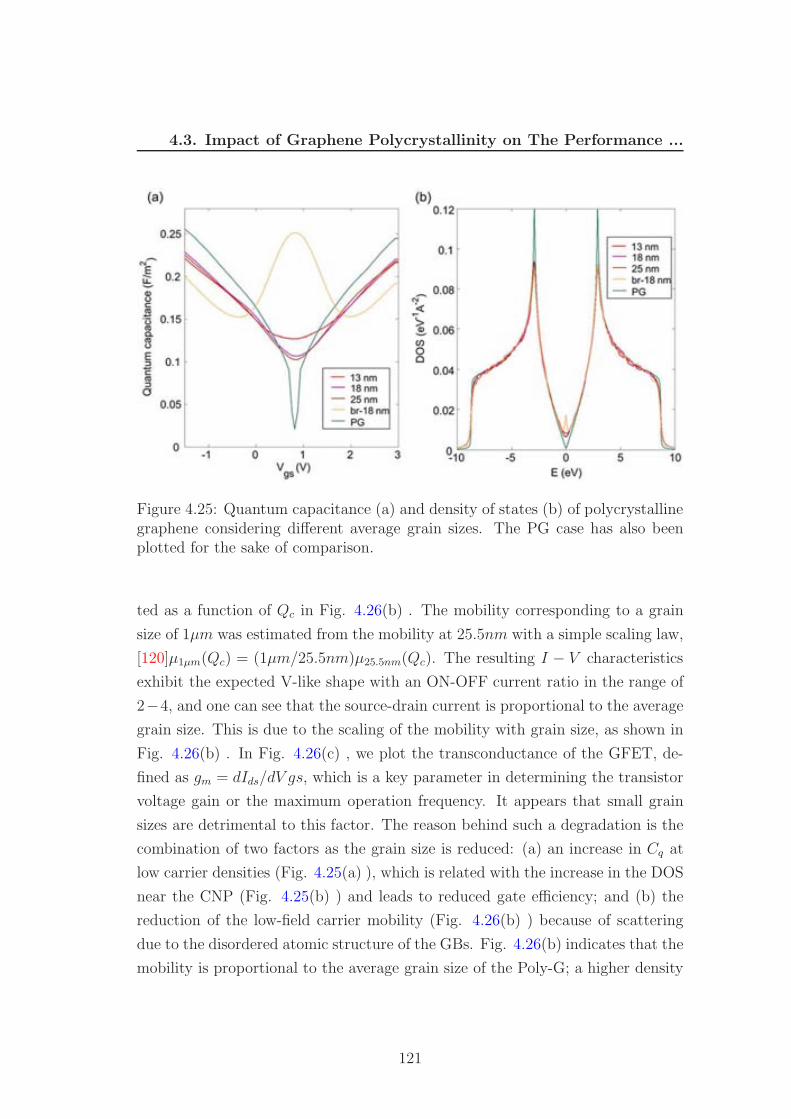
4.3. Impact of Graphene Polycrystallinity on The Performance ...
Figure 4.25: Quantum capacitance (a) and density of states (b) of polycrystallinegraphene considering different average grain sizes. The PG case has also beenplotted for the sake of comparison.
ted as a function of Qc in Fig. 4.26(b) . The mobility corresponding to a grain
size of 1µm was estimated from the mobility at 25.5nm with a simple scaling law,
[120]µ1µm(Qc) = (1µm/25.5nm)µ25.5nm(Qc). The resulting I − V characteristics
exhibit the expected V-like shape with an ON-OFF current ratio in the range of
2−4, and one can see that the source-drain current is proportional to the average
grain size. This is due to the scaling of the mobility with grain size, as shown in
Fig. 4.26(b) . In Fig. 4.26(c) , we plot the transconductance of the GFET, de-
fined as gm = dIds/dV gs, which is a key parameter in determining the transistor
voltage gain or the maximum operation frequency. It appears that small grain
sizes are detrimental to this factor. The reason behind such a degradation is the
combination of two factors as the grain size is reduced: (a) an increase in Cq at
low carrier densities (Fig. 4.25(a) ), which is related with the increase in the DOS
near the CNP (Fig. 4.25(b) ) and leads to reduced gate efficiency; and (b) the
reduction of the low-field carrier mobility (Fig. 4.26(b) ) because of scattering
due to the disordered atomic structure of the GBs. Fig. 4.26(b) indicates that the
mobility is proportional to the average grain size of the Poly-G; a higher density
121
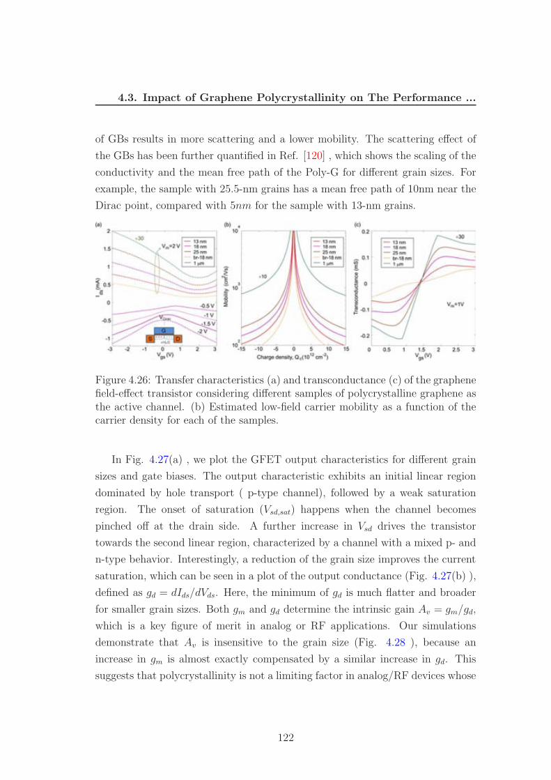
4.3. Impact of Graphene Polycrystallinity on The Performance ...
of GBs results in more scattering and a lower mobility. The scattering effect of
the GBs has been further quantified in Ref. [120] , which shows the scaling of the
conductivity and the mean free path of the Poly-G for different grain sizes. For
example, the sample with 25.5-nm grains has a mean free path of 10nm near the
Dirac point, compared with 5nm for the sample with 13-nm grains.
Figure 4.26: Transfer characteristics (a) and transconductance (c) of the graphenefield-effect transistor considering different samples of polycrystalline graphene asthe active channel. (b) Estimated low-field carrier mobility as a function of thecarrier density for each of the samples.
In Fig. 4.27(a) , we plot the GFET output characteristics for different grain
sizes and gate biases. The output characteristic exhibits an initial linear region
dominated by hole transport ( p-type channel), followed by a weak saturation
region. The onset of saturation (Vsd,sat) happens when the channel becomes
pinched off at the drain side. A further increase in Vsd drives the transistor
towards the second linear region, characterized by a channel with a mixed p- and
n-type behavior. Interestingly, a reduction of the grain size improves the current
saturation, which can be seen in a plot of the output conductance (Fig. 4.27(b) ),
defined as gd = dIds/dVds. Here, the minimum of gd is much flatter and broader
for smaller grain sizes. Both gm and gd determine the intrinsic gain Av = gm/gd,
which is a key figure of merit in analog or RF applications. Our simulations
demonstrate that Av is insensitive to the grain size (Fig. 4.28 ), because an
increase in gm is almost exactly compensated by a similar increase in gd. This
suggests that polycrystallinity is not a limiting factor in analog/RF devices whose
122
4.3. Impact of Graphene Polycrystallinity on The Performance ...
performance depends on the intrinsic gain. However, there are other performance
metrics, such as the intrinsic cutoff (fT ) and maximum frequencies (fmax), which
are severely degraded by the presence of GBs. To demonstrate this, we have
calculated both fT and fmax for the device under consideration, but assuming a
channel length of 100nm. The cutoff frequency is given by fT ≈ gm/2πCgs , where
Cgs is the gate-to-source capacitance. 12 Given that the geometrical capacitance
Ct is much smaller than the quantum capacitance Cq, Cgs∼= Ct. The maximum
frequency is given by fmax ≈ gm/(4πCgs
√
gd(RS +RG), where RS and RG are
the source and gate resistances, respectively. [222] Here, we have assumed state
of the art values, such as [227] RS ∼ 100Ω.µm and RG ∼ 6Ω . As shown in Fig.
4.29, fmax and fT are degraded by one and two orders of magnitude, respectively,
when the average grain size decreases from 1µm to 25nm.
Figure 4.27: Output characteristics (a) and output conductance (b) of thegraphene field-effect transistor considering different samples of polycrystallinegraphene as the active channel.
Realistic GFETs are limited in performance by interaction with the substrate
and top gates. Comparing with the extracted mobility from some reported state-
of-the-art devices, [228] our calculations, which represent the limiting case of
uncovered graphene, overestimate the mobility of these devices by ∼ 10×. As a
consequence, gm, gd, and fT should be reduced by that amount when considering
substrate and top gate effects. Meanwhile, Av is expected to remain constant and
123
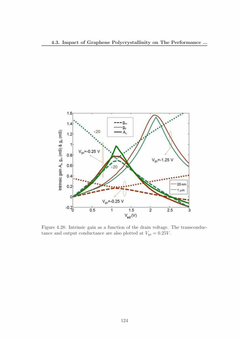
4.3. Impact of Graphene Polycrystallinity on The Performance ...
Figure 4.28: Intrinsic gain as a function of the drain voltage. The transconduc-tance and output conductance are also plotted at Vgs = 0.25V .
124
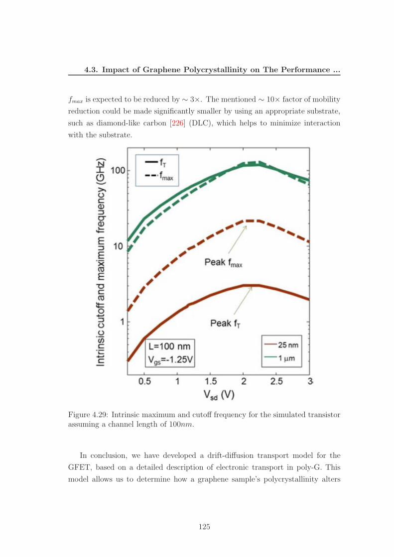
4.3. Impact of Graphene Polycrystallinity on The Performance ...
fmax is expected to be reduced by ∼ 3×. The mentioned ∼ 10× factor of mobility
reduction could be made significantly smaller by using an appropriate substrate,
such as diamond-like carbon [226] (DLC), which helps to minimize interaction
with the substrate.
Figure 4.29: Intrinsic maximum and cutoff frequency for the simulated transistorassuming a channel length of 100nm.
In conclusion, we have developed a drift-diffusion transport model for the
GFET, based on a detailed description of electronic transport in poly-G. This
model allows us to determine how a graphene sample’s polycrystallinity alters
125
4.4. Transport Properties of Amorphous Graphene
the electronic transport in GFETs, enabling the prediction and optimization of
various figures of merit for these devices. We have found that the presence of
GBs produces a severe degradation of both the maximum frequency and the
cutoff frequency, while the intrinsic gain remains insensitive to the presence of
GBs. Overall, polycrystallinity is predicted to be an undesirable trait in GFETs
targeting analog or RF applications.
4.4 Transport Properties of Amorphous Graphene
4.4.1 Introduction
The physics of disordered graphene is at the heart of many fascinating properties
such as Klein tunneling, weak antilocalization or anomalous quantum Hall effect
(see reviews [229, 4]). The precise understanding of individual defects on elec-
tronic and transport properties of graphene is currently of great interest [34]. For
instance, graphene samples obtained by large-scale production methods display a
huge quantity of structural imperfections and defects which jeopardize the robust-
ness of the otherwise exceptionally high charge mobilities of their pristine coun-
terparts [110]. Indeed, the lattice mismatch-induced strain between graphene and
the underlying substrate generates polycrystalline graphene with grain boundaries
which strongly impact on transport properties [41]. However, despite the large
amount of disorder, such graphene flakes usually maintain a finite conductivity
down to very low temperatures (when deposited onto oxide substrates) owing
to electron-hole puddles (charge inohomogeneities fluctuations)-induced perco-
lation effects which limit localization phenomena [2]. The predicted Anderson
localization in two-dimensional disordered graphene has been hard to measure in
non intentionally damaged graphene, in contrast to chemically modified graphene
[230, 231]. In a recent experiment, it was however possible to screen out electron-
holes puddles using sandwiched graphene in between two boron-nitride layers,
together with an additional graphene control layer [113]. As a result of pud-
dles screening, a large increase of the resistivity was obtained at the Dirac point,
evidencing an onset of the Anderson localization regime.
Beyond individual defects and polycrystallinity, a higher level of disorder can
126
4.4. Transport Properties of Amorphous Graphene
be induced on graphene to the point of obtaining two-dimensional amorphous
networks composed of sp2 hybridized carbon atoms. Such networks contain rings
other than hexagons in a disordered arrangement. The average ring size is six ac-
cording to Euler’s theorem, allowing such a system to exist as a flat 2D structure.
Experimentally, such amorphous two-dimensional lattices have been obtained in
electron-beam irradiation experiments [15], and directly visualized by high res-
olution electron transmission microscopy. Previously, indirect evidence for the
formation of an amorphous network was obtained by Raman spectroscopy in
samples subject to electron-beam irradiation [232], ozone exposure [233] and ion
irradiation [234]. In all these cases, an evolution from polycrystalline to amor-
phous structures was observed upon increase of the damage treatment. In [234],
further evidence of the formation of an amorphous network was obtained through
transport measurements. These indicate the transition from a weak localization
regime in the polycrystalline samples to variable range hopping transport in the
strongly localized regime for amorphous samples, as evidenced by the tempera-
ture dependence of the conductivity. Localization lengths were estimated to be
of the range 0.1 to 10 nm in the amorphous samples, depending on the degree of
amorphization. From the theoretical side, models of the amorphous network have
been proposed using stochastic quenching methods [74], and molecular dynamics
[76, 75, 73]. Electronic structure calculations show that the amorphization yields
a large increase of the density of states at and in the environment of the charge
neutrality point [74, 76, 75]. Despite the expected reduction of the conduction
properties due to strong localization effects, Holmstrom et al. [76] suggest that
disorder could enhance metallicity in amorphized samples, in contrast with the
experimental evidence.
Here, we explore the transport properties of two-dimensional sp2 lattices with
massive amount of topological disorder, encoded in a geometrical mixture of
hexagons with pentagon and heptagon rings with a given ring statistics. The
calculations are done using two approaches: a Kubo formulation in which the
conductivity of bulk 2D amorphous graphene lattices was determined, and a
Landauer-Buttiker formulation where the conductance of ribbons of amorphous
graphene contacted to semi-infinite pristine graphene electrodes was calculated.
Both approaches lead to similar findings. Depending on the ratio between odd
127
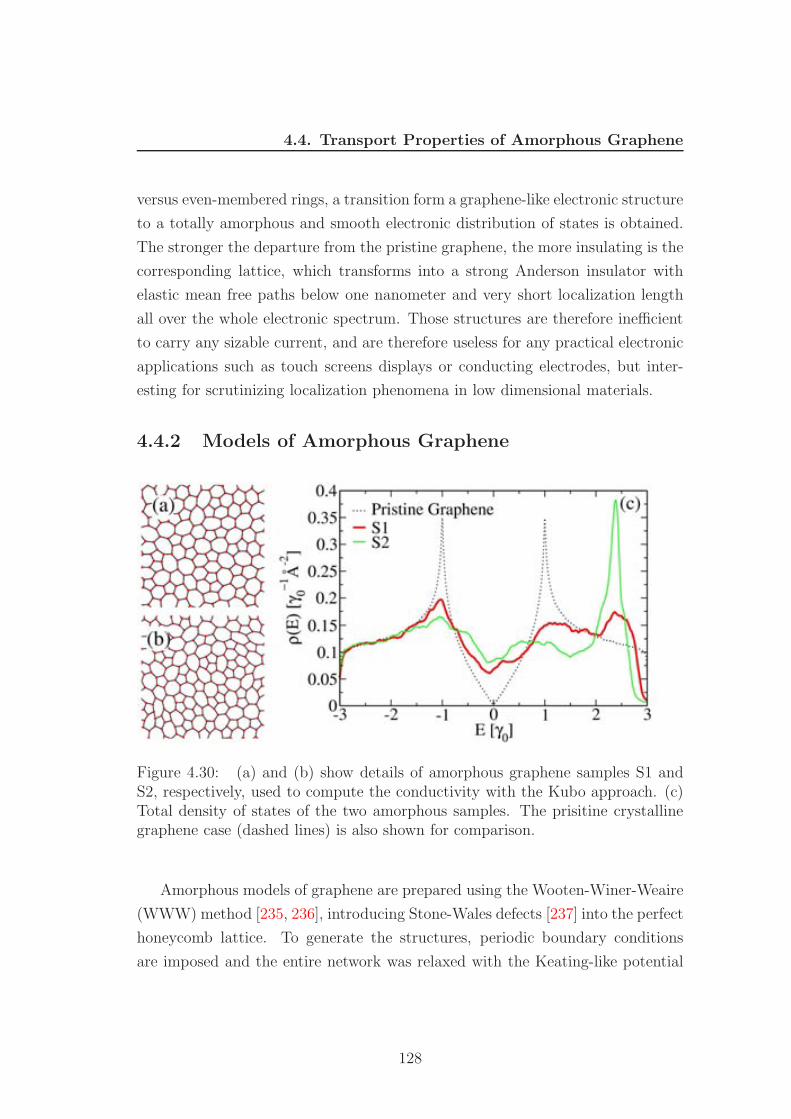
4.4. Transport Properties of Amorphous Graphene
versus even-membered rings, a transition form a graphene-like electronic structure
to a totally amorphous and smooth electronic distribution of states is obtained.
The stronger the departure from the pristine graphene, the more insulating is the
corresponding lattice, which transforms into a strong Anderson insulator with
elastic mean free paths below one nanometer and very short localization length
all over the whole electronic spectrum. Those structures are therefore inefficient
to carry any sizable current, and are therefore useless for any practical electronic
applications such as touch screens displays or conducting electrodes, but inter-
esting for scrutinizing localization phenomena in low dimensional materials.
4.4.2 Models of Amorphous Graphene
Figure 4.30: (a) and (b) show details of amorphous graphene samples S1 andS2, respectively, used to compute the conductivity with the Kubo approach. (c)Total density of states of the two amorphous samples. The prisitine crystallinegraphene case (dashed lines) is also shown for comparison.
Amorphous models of graphene are prepared using the Wooten-Winer-Weaire
(WWW) method [235, 236], introducing Stone-Wales defects [237] into the perfect
honeycomb lattice. To generate the structures, periodic boundary conditions
are imposed and the entire network was relaxed with the Keating-like potential
128
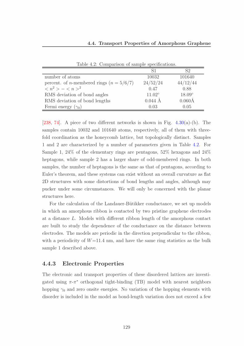
4.4. Transport Properties of Amorphous Graphene
Table 4.2: Comparison of sample specifications.
S1 S2number of atoms 10032 101640percent. of n-membered rings (n = 5/6/7) 24/52/24 44/12/44< n2 > − < n >2 0.47 0.88RMS deviation of bond angles 11.02 18.09
RMS deviation of bond lengths 0.044 A 0.060AFermi energy (γ0) 0.03 0.05
[238, 74]. A piece of two different networks is shown in Fig. 4.30(a)-(b). The
samples contain 10032 and 101640 atoms, respectively, all of them with three-
fold coordination as the honeycomb lattice, but topologically distinct. Samples
1 and 2 are characterized by a number of parameters given in Table 4.2. For
Sample 1, 24% of the elementary rings are pentagons, 52% hexagons and 24%
heptagons, while sample 2 has a larger share of odd-membered rings. In both
samples, the number of heptagons is the same as that of pentagons, according to
Euler’s theorem, and these systems can exist without an overall curvature as flat
2D structures with some distortions of bond lengths and angles, although may
pucker under some circumstances. We will only be concerned with the planar
structures here.
For the calculation of the Landauer-Butikker conductance, we set up models
in which an amorphous ribbon is contacted by two pristine graphene electrodes
at a distance L. Models with different ribbon length of the amorphous contact
are built to study the dependence of the conductance on the distance between
electrodes. The models are periodic in the direction perpendicular to the ribbon,
with a periodicity of W=11.4 nm, and have the same ring statistics as the bulk
sample 1 described above.
4.4.3 Electronic Properties
The electronic and transport properties of these disordered lattices are investi-
gated using π-π∗ orthogonal tight-binding (TB) model with nearest neighbors
hopping γ0 and zero onsite energies. No variation of the hopping elements with
disorder is included in the model as bond-length variation does not exceed a few
129
4.4. Transport Properties of Amorphous Graphene
percent (cf. Table 4.2); all dependence on disorder stems from the ring statistics
which is the dominating effect. Fig. 4.30(c) shows the density of states (DOS)
of the two disordered samples, together with the pristine case (dashed line) for
comparison. Sample 1, which keeps 52% of hexagonal rings, displays several no-
ticeable features, similar to those found in previous studies [74, 76]. First, the
DOS at the charge neutrality point is found to be increased by a large amount.
Additionally, the electron-hole symmetry of the band structure is broken due to
the presence of odd-membered rings and the resonant states that these induce
[72]. The hole part of the spectrum is still reminiscent of the graphene DOS, with
a smoothened peak at the van Hove singularity while in the electron part a second
maximum appears close to the upper conduction band edge. By reducing further
the ratio of even versus odd-membered rings (Sample 2), the second maximum
develops to a strong peak at about E = 2.5γ0 while spectral weight at E = 3γ0
is suppressed. The redistribution of DOS at the upper conduction band edge is
a signature of odd-membered rings and its strength with increasing number of
such rings relates the statistical distribution of rings with the DOS features.
Transport Methodology.- To explore quantum transport in these topologically
disordered graphene bulk samples, we employ a real-space order-N quantum
wavepacket evolution aproach in Chapter 3 to compute the Kubo-Greenwood
conductivity [239]. The conductance of amorphous stripes (ribbons) contacted to
graphene electrodes is computed using the Landauer-Buttiker approach [240]:
G(E) = G0T (E) =2e2
hTr[
t†t]
(4.10)
where T (E) and t(E) are the transmission probability and transmission matrix,
respectively, which can be computed from the Green’s function G(E) in the con-
tact region and the broadening Γ(E) of the states due to the interaction with the
left and right electrodes. We calculate the conductance of the ribbon, which is
infinite and periodic in the direction parallel to the interface between the pristine
graphene electrodes and the amorphous ribbons. Despite the very large peri-
odicity of our models, we perform a thorough sampling of the k‖-points in that
direction [241, 242], to obtain the appropriate V-shaped conductance of graphene
in the thermodynamic limit. G is given per supercell of periodicity W=11.4 nm.
130
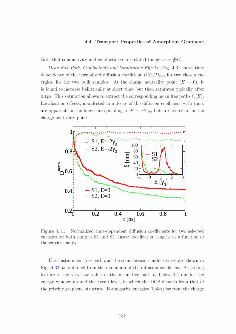
4.4. Transport Properties of Amorphous Graphene
Note that conductivity and conductance are related though σ = LWG.
Mean Free Path, Conductivity and Localization Effects.- Fig. 4.31 shows time
dependence of the normalized diffusion coefficient D(t)/Dmax for two chosen en-
ergies, for the two bulk samples. At the charge neutrality point (E = 0), it
is found to increase ballistically at short time, but then saturates typically after
0.1ps. This saturation allows to extract the corresponding mean free paths ℓe(E).
Localization effects, manifested in a decay of the diffusion coefficient with time,
are apparent for the lines corresponding to E = −2γ0, but are less clear for the
charge neutrality point.
0 0.2 0.4 0.6 0.8 1t [ps]
0.2
0.4
0.6
0.8
1
Dno
rm
S1, E=-2γ0S2, E=-2γ0
-1 0 1 2 3E [γ0]
020406080
100
ξ [n
m] S1
S2
0 0.2 0.4 0.6 0.8 1t [ps]
0.2
0.4
0.6
0.8
1
Dno
rm
S1, E=0S2, E=0
Figure 4.31: Normalized time-dependent diffusion coefficients for two selectedenergies for both samples S1 and S2. Inset: localization lengths as a function ofthe carrier energy
The elastic mean free path and the semiclassical conductivities are shown in
Fig. 4.32, as obtained from the maximum of the diffusion coefficient. A striking
feature is the very low value of the mean free path ℓe below 0.5 nm for the
energy window around the Fermi level, in which the DOS departs from that of
the pristine graphene structure. For negative energies (holes) far from the charge
131
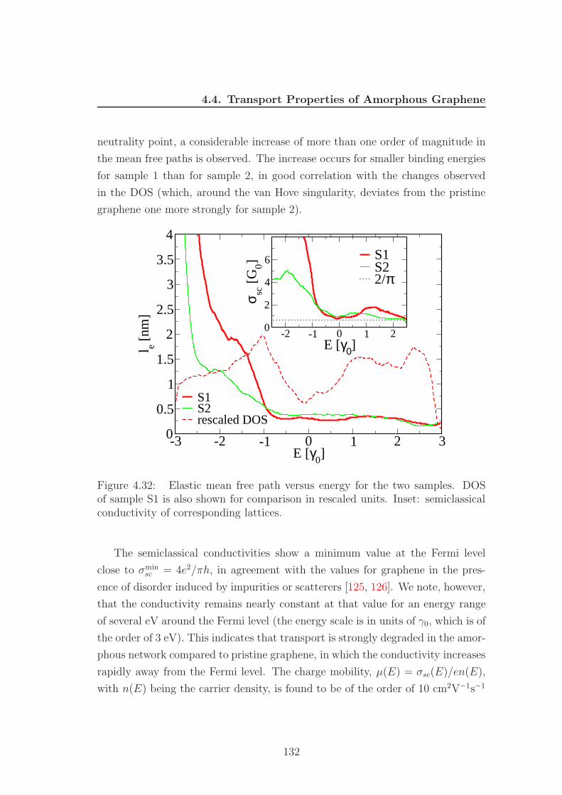
4.4. Transport Properties of Amorphous Graphene
neutrality point, a considerable increase of more than one order of magnitude in
the mean free paths is observed. The increase occurs for smaller binding energies
for sample 1 than for sample 2, in good correlation with the changes observed
in the DOS (which, around the van Hove singularity, deviates from the pristine
graphene one more strongly for sample 2).
-3 -2 -1 0 1 2 3E [γ
0]
0
0.5
1
1.5
2
2.5
3
3.5
4
l e [nm
]
S1S2rescaled DOS
-2 -1 0 1 2E [γ0]
0
2
4
6σ sc
[G0] S1
S22/π
Figure 4.32: Elastic mean free path versus energy for the two samples. DOSof sample S1 is also shown for comparison in rescaled units. Inset: semiclassicalconductivity of corresponding lattices.
The semiclassical conductivities show a minimum value at the Fermi level
close to σminsc = 4e2/πh, in agreement with the values for graphene in the pres-
ence of disorder induced by impurities or scatterers [125, 126]. We note, however,
that the conductivity remains nearly constant at that value for an energy range
of several eV around the Fermi level (the energy scale is in units of γ0, which is of
the order of 3 eV). This indicates that transport is strongly degraded in the amor-
phous network compared to pristine graphene, in which the conductivity increases
rapidly away from the Fermi level. The charge mobility, µ(E) = σsc(E)/en(E),
with n(E) being the carrier density, is found to be of the order of 10 cm2V−1s−1
132
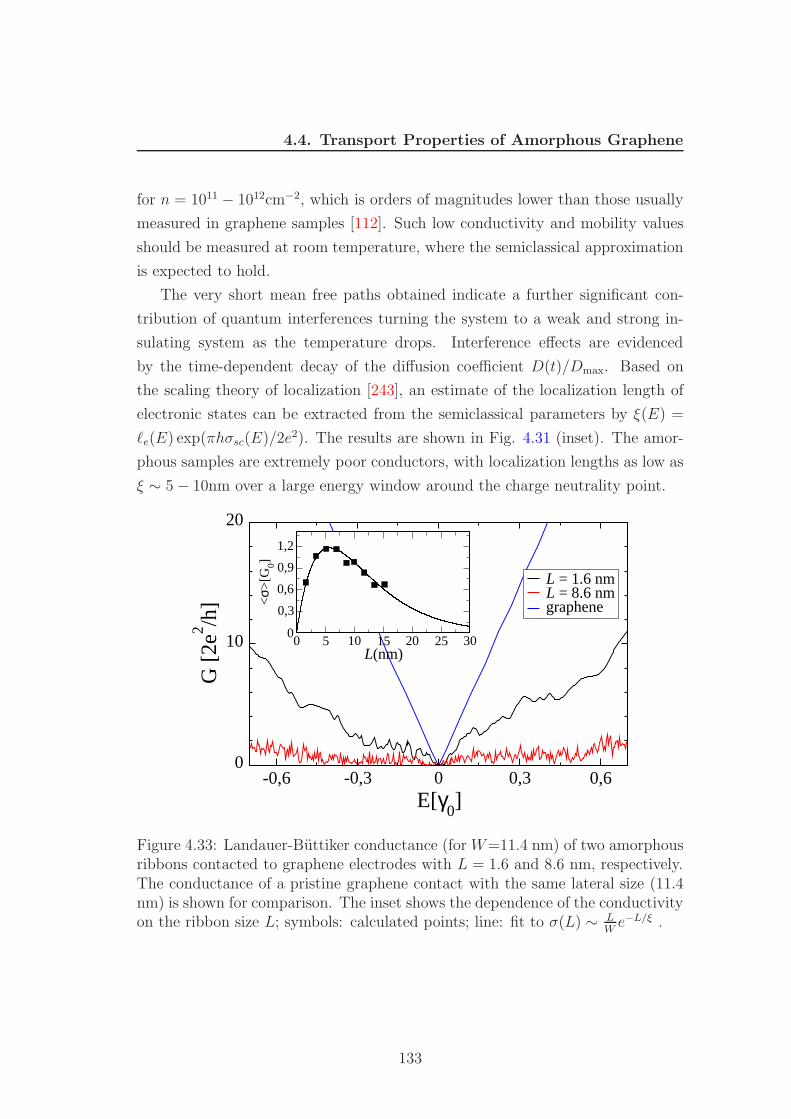
4.4. Transport Properties of Amorphous Graphene
for n = 1011 − 1012cm−2, which is orders of magnitudes lower than those usually
measured in graphene samples [112]. Such low conductivity and mobility values
should be measured at room temperature, where the semiclassical approximation
is expected to hold.
The very short mean free paths obtained indicate a further significant con-
tribution of quantum interferences turning the system to a weak and strong in-
sulating system as the temperature drops. Interference effects are evidenced
by the time-dependent decay of the diffusion coefficient D(t)/Dmax. Based on
the scaling theory of localization [243], an estimate of the localization length of
electronic states can be extracted from the semiclassical parameters by ξ(E) =
ℓe(E) exp(πhσsc(E)/2e2). The results are shown in Fig. 4.31 (inset). The amor-
phous samples are extremely poor conductors, with localization lengths as low as
ξ ∼ 5 − 10nm over a large energy window around the charge neutrality point.
-0,6 -0,3 0 0,3 0,6E[γ
0]
0
10
20
G [2
e2 /h]
L = 1.6 nmL = 8.6 nmgraphene
0 5 10 15 20 25 30L(nm)
0
0,3
0,6
0,9
1,2
<σ>
[G0]
Figure 4.33: Landauer-Buttiker conductance (for W=11.4 nm) of two amorphousribbons contacted to graphene electrodes with L = 1.6 and 8.6 nm, respectively.The conductance of a pristine graphene contact with the same lateral size (11.4nm) is shown for comparison. The inset shows the dependence of the conductivityon the ribbon size L; symbols: calculated points; line: fit to σ(L) ∼ L
We−L/ξ .
133
4.4. Transport Properties of Amorphous Graphene
To further confirm the localization lengths estimated using scaling theory, we
compute explicitly the conductance of the amorphous graphene ribbons contacted
with pristine graphene electrodes, as a function of the ribbon length L. Fig. 4.33
shows the conductance curves for two ribbons of 1.6 and 8.6 nm, respectively,
compared to that of a graphene contact with the same lateral size in the su-
percell (11.4 nm). It is clear that the conductance of the amorphous samples is
greatly reduced with respect to that of graphene, and that the reduction is more
pronounced as the length of the amorphous ribbon becomes larger. Also, while
the conductance for the ribbon with the smallest length is relatively smooth, it
becomes more noisy as the ribbon becomes longer. This reflects the transition
from a diffusive system, in which the ribbon is longer than the mean free path,
but shorter than the localization length, to a strongly localized one in which the
localization length is shorter than the ribbon length.
From the variation of the Landauer-Buttiker conductance with size L, we can
extract reliable values of the localization lengths, as in the Anderson regime the
conductance should decay as G(L) ∼ e−L/ξ. The inset in Fig. 4.33 shows the
value of the conductivity, obtained from the conductance, for each size from 1.6
to 15.3 nm, averaged over an energy window of 1.5γ0 around the Fermi energy.
A fit of the results to σ(L) ∼ LWe−L/ξ yields a value of ξ = 5.8 nm. This value is
consistent with that obtained above using scaling theory, for energies close to the
Fermi level, and confirms that, in these amorphous structures, strong localization
effects should occur at low temperatures at distances of less than 10 nm. These
estimates are in good agreement with the experimental results from transport
measurements by Zhou et al. [234], which show values in the range between 0.1
and 10 nm for samples amorphized by ion radiation.
In conclusion, we have shown that amorphous graphene is a strong Anderson
insulator. The increase of the density of states close to the charge neutrality
point is concomitant with marked quantum interferences which inhibit current
flow at low temperature. Very short mean free paths and localization lengths are
predicted, in line with recent experimental evidence in graphene under heavy ion
irradiation damage [234].
134
Chapter 5
Spin Transport in Disordered
Graphene
Carbon has a weak atomic SOC, so graphene is expected to have long spin re-
laxation time and phase coherence lengths. However, the spin injection measure-
ments based on a non-local spin valve geometry [44, 54, 55] revealed surprisingly
short spin relaxation times of only about 100 − 200ps, being only weakly depen-
dent on the charge density and temperature. The longest spin relaxation time
has been measured up to now is also in the order of a few ns [88]. There are
many explanations for short spin relaxation times in graphene. Some explana-
tions are related to enhanced SOC induced by adatoms in graphene sheet or by
the breaking inversion symmetry due to the electric field created by substrate.
Another possibility could be the Gauge field due to ripples [53] which induces
an effective magnetic field B⊥ perpendicular to the graphene sheet. There is
also another explanation said that the forming of sp3 hybridization enhances lo-
cal spin-orbit coupling [59] which leads to fast spin relaxation. However, these
theoretical results couldn’t give satisfying explanations for experimental data to
date.
In this section, we perform some theoretical calculations to investigate the
spin relaxation in ultra clean graphene, and we propose a new mechanism for
spin relaxation in graphene which is related to the disconnection of spin and
momentum close to the Dirac point. At the final of this Chapter, some results
135
5.1. Spin Transport in Graphene: Pseudospin Driven Spin ...
of the effect of the segregation of strong-SOC adatoms on graphene on Quantum
Hall Effect (QHE) are shown.
5.1 Spin Transport in Graphene: Pseudospin
Driven Spin Relaxation Mechanism
5.1.1 Introduction
The electronic properties of monolayer graphene strongly differ from those of
two-dimensional metals and semiconductors in part because of inherent electron-
hole band structure symmetry and a particular density of states which vanishes
at the Dirac point [59]. Additionally, the sublattice degeneracy and honeycomb
symmetry lead to eigenstates that hold an additional quantum (Berry’s) phase,
associated with the so-called pseudospin quantum degree of freedom. All of these
electronic features are manifested through the Klein tunneling phenomenon [63],
weak antilocalization [61] or the anomalous quantum Hall effect [244]. The possi-
bility of using the pseudospin as a means to transport and store information has
also been theoretically proposed [245, 246]. There, the role of the pseudospin is
equivalent to that of the spin in spintronics, such as in the pseudospin analogue
of the giant magnetoresistance in bilayer graphene [246].
Even though pseudospin-related effects drive most of the unique transport sig-
natures of graphene, the role of the pseudospin on the spin relaxation mechanism
has not been explicitly addressed and quantified. Pseudospin and spin dynamics
are usually perceived as decoupled from each other, with pseudospin lifetimes
being much shorter and pseudospin dynamics much faster than those for spins.
However, this picture breaks down in the vicinity of the Dirac point, a region
that is usually out of reach of perturbative approaches and that is particularly
relevant for experiments, because Fermi energies can only be shifted by about
0.3 eV via electrostatic gating. Moreover, in the presence of SOC, spin couples
to orbital motion, and therefore to pseudospin [84], so that spin and pseudospin
dynamics should not be treated independently.
The reason for overlooking the role of the pseudospin on the spin dynamics
136
5.1. Spin Transport in Graphene: Pseudospin Driven Spin ...
is perhaps rooted in the fact that the spin transport properties appear remark-
ably similar to those found in common metals and semiconductors [247]. Indeed,
spin precession measurements in nonlocal devices result in experimental signa-
tures that would be indistinguishable from those obtained in a metal such as
aluminium [248], or a semiconductor such as GaAs [249], with extracted spin
relaxation times τs that are also typically of the same order of magnitude (a few
nanoseconds or lower). Spin relaxation in graphene has therefore been interpreted
using the conventional experimental manifestations of either the Elliot-Yafet (EY)
or Dyakonov-Perel (DP) mechanism [45, 46, 47, 11, 250]. In the EY scenario, the
spin relaxation time is determined by the spin mixing of carriers and the SOC
of the scattering potential, and thus it is usually assumed to be proportional to
the momentum relaxation time as τs ≈ α · τp , with α≫ 1 (for instance in alkali
metals α ∼ 104 − 106) [247]. In contrast, in the DP mechanism spin precesses
about an effective magnetic field whose orientation is fixed by the momentum
direction during free propagation of electrons. Such orientation changes at each
scattering event, which results in a different scaling behavior as 1/τDPs ∼ Ω2τp
[247] (with Ω the average magnitude of the intrinsic Larmor frequency over the
momentum distribution). Experimental estimates of τs and τp are generally ob-
tained in a phenomenological way by fitting the experimental resistivity curves to
the theoretical formula obtained using semi-classical transport equations [44, 46].
However, this phenomenological analysis is not well connected with the micro-
scopic interpretation. First of all, the weak SOC in graphene would suggest τs in
the microsecond range [10, 43], in clear disagreement with experimental data. In
addition, the τs estimated in high-mobility graphene with long mean free paths
remains unsatisfactorily interpreted with a single relaxation mechanism, say EY
or DP [47, 90, 251]. The suppression of τs in clean graphene has been tenta-
tively associated to an enhanced (intrinsic or extrinsic) spin-orbit coupling due
to mechanical deformations such as ripples, or unavoidable adatoms incorporated
during the device fabrication process, but the ultimate and microscopic nature of
spin relaxation at play remains controversial and elusive.
Here, we unravel a spin relaxation mechanism for nonmagnetic samples that
follows from an entanglement of spin and pseudospin degrees of freedom driven by
random SOC, which makes it unique to graphene and is markedly different from
137
5.1. Spin Transport in Graphene: Pseudospin Driven Spin ...
conventional processes. We show that the mixing between spin and pseudospin-
related Berry’s phases results in unexpectedly fast spin dephasing, even when
approaching the ballistic limit, and leads to increasing spin relaxation times away
from the Dirac point, as observed experimentally. This hitherto unknown phe-
nomenon points towards revisiting the origin of the small spin relaxation times
found in graphene, where SOC can be caused by adsorbed adatoms, ripples or
even the substrate. It also opens new perspectives for spin manipulation us-
ing the pseudospin degree of freedom (or vice versa), a tantalizing quest for the
emergence of radically new information storage and processing technologies.
5.1.2 Spin Relaxation in Gold-Decorated Graphene
In the following, we explore spin characteristics in graphene by investigating
the effect of weak perturbation induced by low densities of ad-atoms (down to
1012cm−2), which introduce a random Rashba field in real space but vanishingly
small intervalley scattering, yielding long mean free paths. Here, for typical
electron densities within [1010, 1012]cm−2, the Fermi wavelength (λF = 2√
π/n,
n the charge density) lies between 20 and 200 nm and thus exceeds the mean
separation between adatoms (∼ 10nm) where spin-orbit scattering occurs, there-
fore questioning the use of a standard semiclassical description. To study spin
dynamics (and spin relaxation), we use a non-perturbative method by solving
the full time-dependent evolution of initially spin polarized wavepackets, either
through a direct diagonalization of a continuum model, or a real space algorithm
for a microscopic disorder model, defined in a tight-binding basis. We describe
the system of a graphene monolayer functionalized with a random distribution
of adatoms. The electronic structure of clean graphene is captured by the usual
π-π* orthogonal tight-binding model (with a single pz-orbital per carbon site,
zero onsite energies and nearest neighbors hopping γ0). The presence of non-
magnetic adatoms randomly adsorbed at the hollow positions on the graphene
sheet introduces additional local spin-orbit coupling terms (Fig. 5.1a,b), defined
as [29].
138
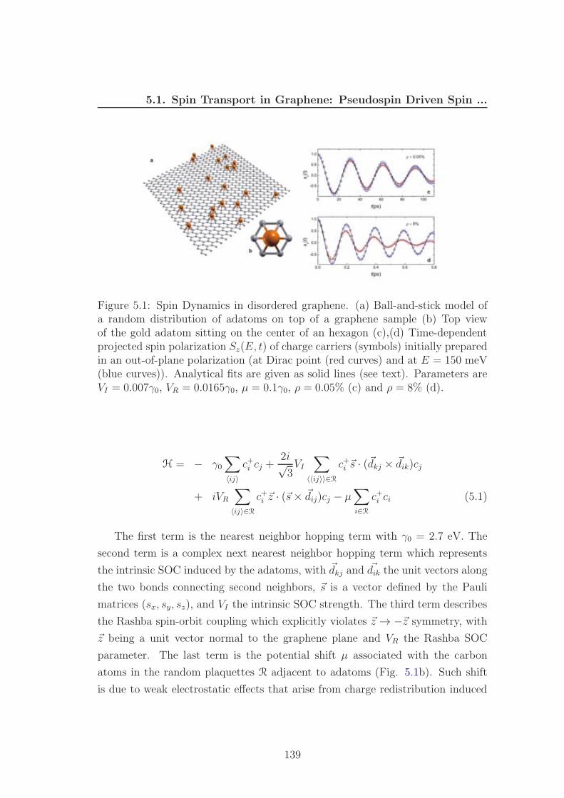
5.1. Spin Transport in Graphene: Pseudospin Driven Spin ...
Figure 5.1: Spin Dynamics in disordered graphene. (a) Ball-and-stick model ofa random distribution of adatoms on top of a graphene sample (b) Top viewof the gold adatom sitting on the center of an hexagon (c),(d) Time-dependentprojected spin polarization Sz(E, t) of charge carriers (symbols) initially preparedin an out-of-plane polarization (at Dirac point (red curves) and at E = 150 meV(blue curves)). Analytical fits are given as solid lines (see text). Parameters areVI = 0.007γ0, VR = 0.0165γ0, µ = 0.1γ0, ρ = 0.05% (c) and ρ = 8% (d).
H = − γ0∑
〈ij〉
c+i cj +2i√
3VI
∑
〈〈ij〉〉∈R
c+i ~s · (~dkj × ~dik)cj
+ iVR∑
〈ij〉∈R
c+i ~z · (~s× ~dij)cj − µ∑
i∈R
c+i ci (5.1)
The first term is the nearest neighbor hopping term with γ0 = 2.7 eV. The
second term is a complex next nearest neighbor hopping term which represents
the intrinsic SOC induced by the adatoms, with ~dkj and ~dik the unit vectors along
the two bonds connecting second neighbors, ~s is a vector defined by the Pauli
matrices (sx, sy, sz), and VI the intrinsic SOC strength. The third term describes
the Rashba spin-orbit coupling which explicitly violates ~z → −~z symmetry, with
~z being a unit vector normal to the graphene plane and VR the Rashba SOC
parameter. The last term is the potential shift µ associated with the carbon
atoms in the random plaquettes R adjacent to adatoms (Fig. 5.1b). Such shift
is due to weak electrostatic effects that arise from charge redistribution induced
139
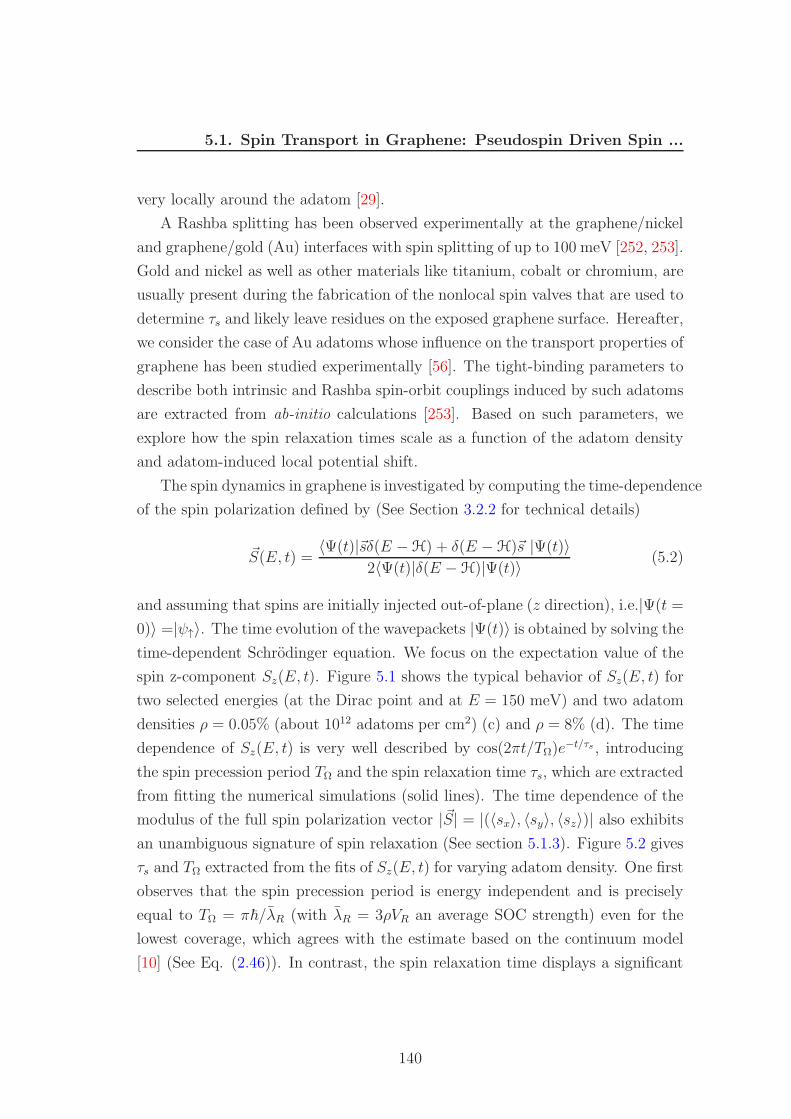
5.1. Spin Transport in Graphene: Pseudospin Driven Spin ...
very locally around the adatom [29].
A Rashba splitting has been observed experimentally at the graphene/nickel
and graphene/gold (Au) interfaces with spin splitting of up to 100 meV [252, 253].
Gold and nickel as well as other materials like titanium, cobalt or chromium, are
usually present during the fabrication of the nonlocal spin valves that are used to
determine τs and likely leave residues on the exposed graphene surface. Hereafter,
we consider the case of Au adatoms whose influence on the transport properties of
graphene has been studied experimentally [56]. The tight-binding parameters to
describe both intrinsic and Rashba spin-orbit couplings induced by such adatoms
are extracted from ab-initio calculations [253]. Based on such parameters, we
explore how the spin relaxation times scale as a function of the adatom density
and adatom-induced local potential shift.
The spin dynamics in graphene is investigated by computing the time-dependence
of the spin polarization defined by (See Section 3.2.2 for technical details)
~S(E, t) =〈Ψ(t)|~sδ(E −H) + δ(E −H)~s |Ψ(t)〉
2〈Ψ(t)|δ(E −H)|Ψ(t)〉 (5.2)
and assuming that spins are initially injected out-of-plane (z direction), i.e.|Ψ(t =
0)〉 =|ψ↑〉. The time evolution of the wavepackets |Ψ(t)〉 is obtained by solving the
time-dependent Schrodinger equation. We focus on the expectation value of the
spin z-component Sz(E, t). Figure 5.1 shows the typical behavior of Sz(E, t) for
two selected energies (at the Dirac point and at E = 150 meV) and two adatom
densities ρ = 0.05% (about 1012 adatoms per cm2) (c) and ρ = 8% (d). The time
dependence of Sz(E, t) is very well described by cos(2πt/TΩ)e−t/τs , introducing
the spin precession period TΩ and the spin relaxation time τs, which are extracted
from fitting the numerical simulations (solid lines). The time dependence of the
modulus of the full spin polarization vector |~S| = |(〈sx〉, 〈sy〉, 〈sz〉)| also exhibits
an unambiguous signature of spin relaxation (See section 5.1.3). Figure 5.2 gives
τs and TΩ extracted from the fits of Sz(E, t) for varying adatom density. One first
observes that the spin precession period is energy independent and is precisely
equal to TΩ = π~/λR (with λR = 3ρVR an average SOC strength) even for the
lowest coverage, which agrees with the estimate based on the continuum model
[10] (See Eq. (2.46)). In contrast, the spin relaxation time displays a significant
140
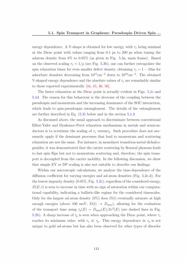
5.1. Spin Transport in Graphene: Pseudospin Driven Spin ...
energy dependence. A V-shape is obtained for low energy, with τs being minimal
at the Dirac point with values ranging from 0.1 ps to 200 ps when tuning the
adatom density from 8% to 0.05% (as given in Fig. 5.3a, main frame). Based
on the observed scaling τs ∼ 1/ρ (see Fig. 5.3b), one can further extrapolate the
spin relaxation times for even smaller defect density, obtaining τs ∼ 1 − 10ns for
adsorbate densities decreasing from 1011cm−2 down to 1010cm−2. The obtained
V-shaped energy dependence and the absolute values of τs are remarkably similar
to those reported experimentally [44, 45, 46, 56].
The faster relaxation at the Dirac point is actually evident in Figs. 5.1c and
5.1d. The reason for this behaviour is the decrease of the coupling between the
pseudospin and momentum and the increasing dominance of the SOC interaction,
which leads to spin-pseudospin entanglement. The details of the entanglement
are further described in Eq. (5.3) below and in the section 5.1.3
As discussed above, the usual approach to discriminate between conventional
Elliot-Yafet and Dyakonov-Perel relaxation mechanisms in metals and semicon-
ductors is to scrutinize the scaling of τs versusτp. Such procedure does not nec-
essarily apply if the dominant processes that lead to momentum and scattering
relaxation are not the same. For instance, in monolayer transition-metal dichalco-
genides, it was demonstrated that the carrier scattering by flexural phonons leads
to fast spin flips but not to momentum scattering and, therefore, the spin trans-
port is decoupled from the carrier mobility. In the following discussion, we show
that simple EY or DP scaling is also not suitable to describe our findings.
Within our microscopic calculations, we analyze the time-dependence of the
diffusion coefficient for varying energies and ad-atom densities (Fig. 5.2c,d). For
the lowest impurity density (0.05%, Fig. 5.2c), regardless of the considered energy,
D(E, t) is seen to increase in time with no sign of saturation within our computa-
tional capability, indicating a ballistic-like regime for the considered timescales.
Only for the largest ad-atom density (8%) does D(t) eventually saturate at high
enough energies (above 100 meV, D(t) → Dmax), allowing for the evaluation
of the transport time using τp(E) = Dmax(E)/2v2(E) (see dashed lines in Fig.
5.2b). A sharp increase of τp is seen when approaching the Dirac point, where τs
reaches its minimum value, with τs ≪ τp. This energy dependence in τp is not
unique to gold ad-atoms but has also been observed for other types of disorder
141
5.1. Spin Transport in Graphene: Pseudospin Driven Spin ...
Figure 5.2: Spin relaxation times and transport mechanisms. Spin relaxationtimes (τs) for ρ = 0.05% (a) and ρ = 8% (b). Black (red) solid symbols indicateτs for µ = 0.1γ0 (µ = 0.2γ0). TΩ vs. E is also shown (open symbols). τp(dotted line in (b)) is shown over a wider energy range (top x-axis) in order tostress the divergence around E = 0 (µ = 0.2γ0). We cannot evaluate τp below 100meV, since the diffusive regime is not established within our computational reach.Panels (c) and (d): Time dependent diffusion coefficient D(t) for ρ = 0.05% andρ = 8% with µ = 0.2γ0.
142
5.1. Spin Transport in Graphene: Pseudospin Driven Spin ...
with a weak intervalley scattering contribution, such as epoxide defects or long
range scatterers [4]. As seen in Fig. 5.3b, τs ∼ 1/ρ, which does not allow us to
discriminate between EY and DP processes. However, the absolute values of τs
and τp (with τs ≪ τp) are a clear manifestation of the breakdown of the typical
scaling associated to both mechanisms. Even the unconventional DP regime de-
scribed in Ref. [247] for the case of τp/TΩ ≥ 1 where 1/τs ∼ ∆Ω (with ∆Ω an
effective width of the distribution of precession frequencies) cannot account for
the observation that a weak variation in the local disorder affects the absolute
values of τs (while ρ is unchanged) as observed in Fig. 5.2. Here local disorder
is monitored by the µ parameter. (Although µ belongs to the TB parameteriza-
tion of the adatom, we use it temporarily to increase local disorder.) In fact, its
value could slightly change when modifying the substrate screening or in presence
of a more strongly bonded adsorbant than Au. As a consequence of the above
findings, the spin relaxation mechanism at play is incompatible with both the
Elliot-Yafet and the Dyakonov-Perel mechanisms, a fact which could shed new
light on the current debate on the microscopic nature of spin relaxation in clean
graphene [47, 90, 251].
We now further study the origin of the τs minimum at low energy and its
unconventional scaling with τp. Given that our simulations with the microscopic
model give τs ≪ τp, we further explore the low-energy spin dynamics with an
effective continuum model, in which the spin-orbit scattering is treated as a ho-
mogeneous potential [10]. We solve the Dirac equation in the continuum model
by using a 4× 4 effective Hamiltonian, taking into account the pseudospin degree
of freedom
h(~k) = h0(~k) + hR(~k) + hI(~k) (5.3)
While the hopping from three nearest neighbors h0(~k) = ~vF (ζσxkx + σyky) ⊗ 1s
dominates at high energy and vanishes at the Dirac point (ζ = ±1 for K
and K ′ valleys, ~σ are pseudospin Pauli matrices and 1s is a 2 × 2 identity
matrix), the intrinsic SOC hI(~k) = λIζ [σz ⊗ sz] and the Rashba interaction
hR(~k) = λR (ζ [σx ⊗ sy] − [σy ⊗ sx]) play an extremely important role at the Dirac
point, where the coupling between spin and pseudospin becomes predominant,
143
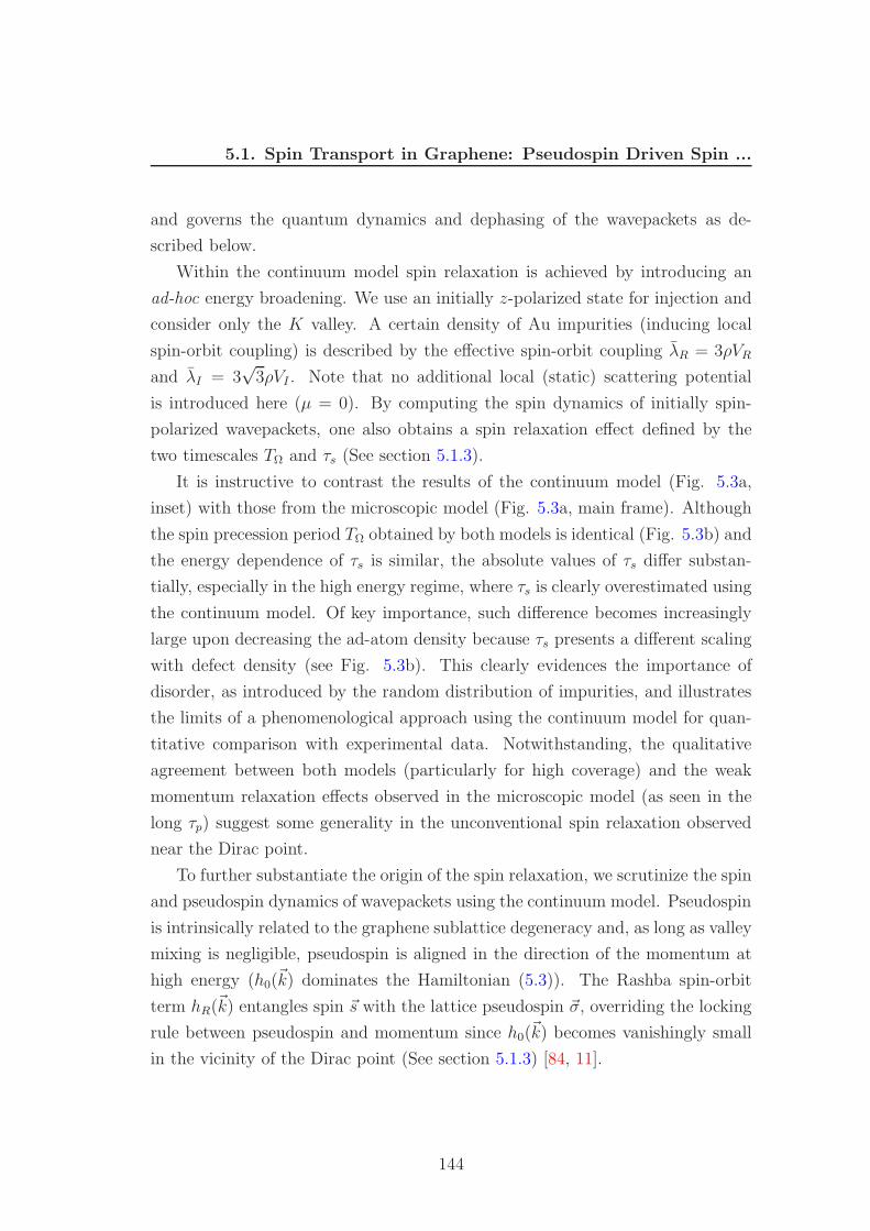
5.1. Spin Transport in Graphene: Pseudospin Driven Spin ...
and governs the quantum dynamics and dephasing of the wavepackets as de-
scribed below.
Within the continuum model spin relaxation is achieved by introducing an
ad-hoc energy broadening. We use an initially z-polarized state for injection and
consider only the K valley. A certain density of Au impurities (inducing local
spin-orbit coupling) is described by the effective spin-orbit coupling λR = 3ρVR
and λI = 3√
3ρVI . Note that no additional local (static) scattering potential
is introduced here (µ = 0). By computing the spin dynamics of initially spin-
polarized wavepackets, one also obtains a spin relaxation effect defined by the
two timescales TΩ and τs (See section 5.1.3).
It is instructive to contrast the results of the continuum model (Fig. 5.3a,
inset) with those from the microscopic model (Fig. 5.3a, main frame). Although
the spin precession period TΩ obtained by both models is identical (Fig. 5.3b) and
the energy dependence of τs is similar, the absolute values of τs differ substan-
tially, especially in the high energy regime, where τs is clearly overestimated using
the continuum model. Of key importance, such difference becomes increasingly
large upon decreasing the ad-atom density because τs presents a different scaling
with defect density (see Fig. 5.3b). This clearly evidences the importance of
disorder, as introduced by the random distribution of impurities, and illustrates
the limits of a phenomenological approach using the continuum model for quan-
titative comparison with experimental data. Notwithstanding, the qualitative
agreement between both models (particularly for high coverage) and the weak
momentum relaxation effects observed in the microscopic model (as seen in the
long τp) suggest some generality in the unconventional spin relaxation observed
near the Dirac point.
To further substantiate the origin of the spin relaxation, we scrutinize the spin
and pseudospin dynamics of wavepackets using the continuum model. Pseudospin
is intrinsically related to the graphene sublattice degeneracy and, as long as valley
mixing is negligible, pseudospin is aligned in the direction of the momentum at
high energy (h0(~k) dominates the Hamiltonian (5.3)). The Rashba spin-orbit
term hR(~k) entangles spin ~s with the lattice pseudospin ~σ, overriding the locking
rule between pseudospin and momentum since h0(~k) becomes vanishingly small
in the vicinity of the Dirac point (See section 5.1.3) [84, 11].
144

5.1. Spin Transport in Graphene: Pseudospin Driven Spin ...
Figure 5.3: Spin relaxation times deduced from the continuum and microscopicmodels. (a) Spin relaxation times (τs) for varying ρ between 0.05% and 8%extracted from the microscopic model (with µ = 0.1γ0). Inset: τs values usingthe continuum model for ρ = 1% and 8% (filled symbols). A comparison withthe microscopic model (with µ = 0) is also given for ρ = 8% (open circles).(b) Scaling behavior of TΩ and τs versus 1/ρ. The TΩ values obtained with themicroscopic (resp. continuum) model are given by red diamonds (resp. red solidlines). τs values for the microscopic model (blue squares) and the continuummodel (black circles) are shown for two selected energies E = 150meV (solidsymbols) and E = 0 (open symbols). Solid lines are here guides to the eye.
145
5.1. Spin Transport in Graphene: Pseudospin Driven Spin ...
Figure 5.4: Spin and pseudospin dynamics in graphene with ρ = 8% of adatoms.Time dependence of spin-polarization Sz (blue) and pseudospin polarization σz(green) in z projection for energies E = 130meV (a), E = 0 (b), and E = −5 meV(c). Note that all quantities are normalized to their maximum value to bettercontrast them in the same scale. Middle panels show the time evolution for bothspin (from blue to pink) and pseudospin (from green to orange). The snapshotsare taken at different times from t1 to t4 sampling the shaded regions in (a), (b),(c). (d) Fourier transform of Sz(t) plotted over oscillation period, and showingnon-dispersive spectra at high energy (between E =125 meV, 130 meV and 135meV). Low-energy spectra (for E = −5 meV, 0 and 5 meV) change strongly withenergy (dispersive) showing a gradual reduction and blue shift of the originalRashba peak at about 0.19 ps and the appearance of additional features.
146
5.1. Spin Transport in Graphene: Pseudospin Driven Spin ...
Figure 5.4 highlights the spin dynamics at different chosen energies E = 0,
E = −5 meV (low energy) and E = 130 meV (high energy), which are repre-
sentative of the underlying physics (note that no relaxation takes place for fixed
energy, thus the requirement of the ad-hoc broadening). At high energy, the spin
precesses quite regularly as seen in Fig. 5.4a, which shows an oscillatory pattern
of Sz(t) dominated by a single period TΩ = π~/λR =0.19 ps. The spin precession
occurs about an effective magnetic field BR dictated by the Rashba interaction
and pointing tangentially to the Fermi circle (as seen from the precession from
blue to pink in middle panels from t1 to t4). In contrast, the pseudospin 〈~σ(t)〉points approximately in the same direction of the momentum (evolving from green
to orange). Its oscillatory pattern is driven by the Rashba period TΩ together
with a superimposed and more rapid oscillation (described in the section 5.1.3).
The situation at low energy (Fig. 5.4b,c) is markedly different. We observe a
highly unconventional spin and pseudospin motion which is analyzed more closely
for the spin and pseudospin z-components at two low energies (at the Dirac point
and at E = −5 meV). In contrast to the high-energy case, the amplitude of
the pseudospin oscillation is strongly enhanced since pseudospin is no longer
locked with momentum but starts to precess about an effective pseudo-magnetic
field. The pseudo-magnetic field depends strongly on the spin orientation, thus
yielding complex time-dependent dynamics of spin and pseudospin (see middle
panels of Figure 5.4 corresponding to 5.4b,c). Such an effect derives from the
increased pseudospin precession period T ps0 = π~/E (about Bps
0 ), which decreases
significantly at low energy. Therefore 〈σi〉 can no longer be replaced by its time
average 〈σi〉 (in contrast to the high-energy situation, see section 5.1.3), which
in consequence also holds for the Rashba field BR. The time dependence of
BR with variability on a timescale similar to the Rashba period leads then to
strong non-linear dynamics of spin and pseudospin motion. As a result of such
coupled dynamics, the spin precession cannot be described by a single period TΩ
as becomes evident from the complex Fourier spectra of Sz(t) in Fig. 5.4d. The
time dependence of BR includes also changes of its direction, thus impacting the
pseudospin and lifting the pseudospin-momentum locking. Both of these effects
finally produce a joint spin/pseudospin motion prohibiting the de-coupling of
driving forces (B ps0 , BR) that was possible at higher energies.
147
5.1. Spin Transport in Graphene: Pseudospin Driven Spin ...
While the continuum model provides qualitative insight into the spin-pseudospin
coupling and entanglement of their corresponding wavefunctions, the microscopic
model enables the quantification of spin relaxation times for a given microscopic
disorder. By scrutinizing the general form of the spin polarization (Eq. (5.2)), a
simple understanding of the spin relaxation mechanism can be drawn. In the
microscopic model, the propagation of an initially spin-polarized wavepacket
|ψ↑(t = 0)〉, is driven by the evolution operator e−iHt/~|ψ↑(t = 0)〉, with H
consisting of the clean graphene term plus the spin orbit coupling potential,
which acts as a local (and random) perturbation on the electron spin. The time-
dependence of the total spin polarization results from the accumulated dephasing
along scattering trajectories developed under the evolution operator. As the
distribution of scattering centers is random in space, all different trajectories ac-
cumulate different phase shifts in their wavefunctions (each being the result of
local spin/pseudospin coupling and disorder potential). When phase shifts for up
and down components average out, the spin polarization of |ψ↑(t = 0)〉 is lost.
5.1.3 Further Discussion
Low-energy effective Hamiltonian and analysis of electronic states close to the
Dirac point
To illustrate that spin and pseudospin are fully entangled for certain states
close to the Dirac point, we calculate the band structure and the modulus of
the spin polarization vector |~S(~k)|. Fig. 5.5 shows the computed band structure
obtained by diagonalizing the Kane-Mele-Rashba Hamiltonian (Eq.(5.3)) for 8%
gold adatom coverage. The Rashba term induces a counter-propagating spin
texture in the kx, ky plane that tends to vanish close to the Dirac point as [84]:
~Sνµ(~k) =µ~vF (~k × ~z)√
λ2R + ~2v2Fk2
(5.4)
We further calculate the modulus of the spin polarization vector |~S| = |(〈sx〉, 〈sy〉, 〈sz〉)|from the eigenstates of the full Hamiltonian in Eq.(5.3) with both intrinsic and
148
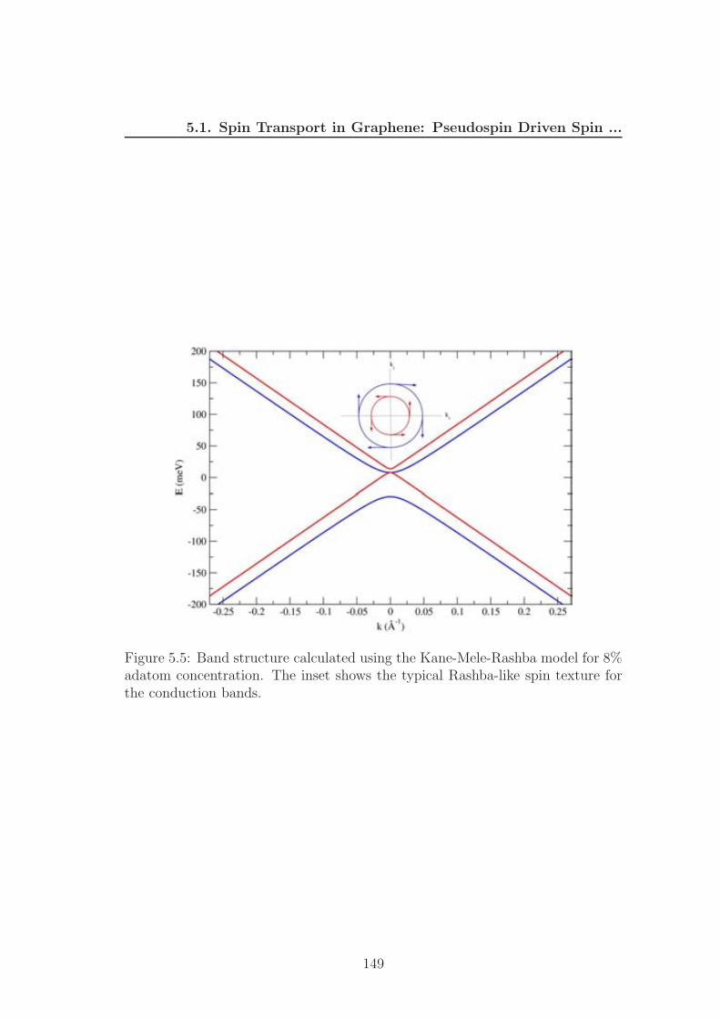
5.1. Spin Transport in Graphene: Pseudospin Driven Spin ...
Figure 5.5: Band structure calculated using the Kane-Mele-Rashba model for 8%adatom concentration. The inset shows the typical Rashba-like spin texture forthe conduction bands.
149
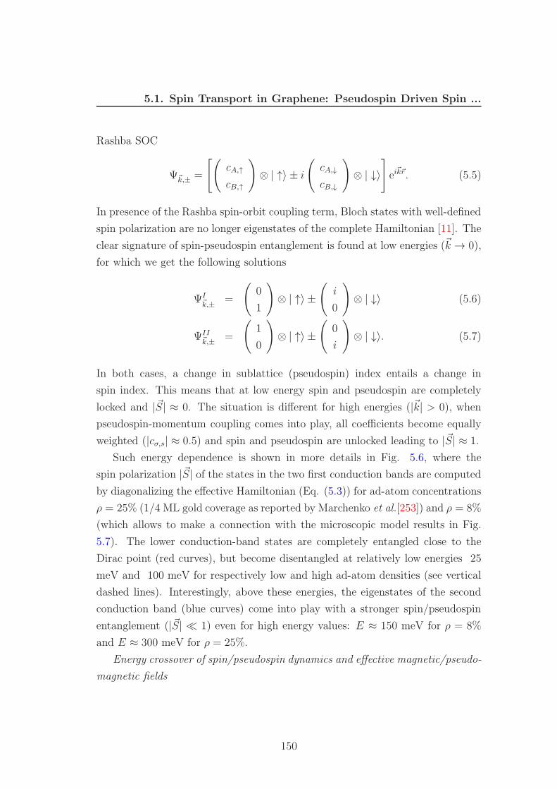
5.1. Spin Transport in Graphene: Pseudospin Driven Spin ...
Rashba SOC
Ψ~k,± =
[(
cA,↑
cB,↑
)
⊗ | ↑〉 ± i
(
cA,↓
cB,↓
)
⊗ | ↓〉]
ei~k~r. (5.5)
In presence of the Rashba spin-orbit coupling term, Bloch states with well-defined
spin polarization are no longer eigenstates of the complete Hamiltonian [11]. The
clear signature of spin-pseudospin entanglement is found at low energies (~k → 0),
for which we get the following solutions
ΨI~k,±
=
(
0
1
)
⊗ | ↑〉 ±(
i
0
)
⊗ | ↓〉 (5.6)
ΨII~k,±
=
(
1
0
)
⊗ | ↑〉 ±(
0
i
)
⊗ | ↓〉. (5.7)
In both cases, a change in sublattice (pseudospin) index entails a change in
spin index. This means that at low energy spin and pseudospin are completely
locked and |~S| ≈ 0. The situation is different for high energies (|~k| > 0), when
pseudospin-momentum coupling comes into play, all coefficients become equally
weighted (|cσ,s| ≈ 0.5) and spin and pseudospin are unlocked leading to |~S| ≈ 1.
Such energy dependence is shown in more details in Fig. 5.6, where the
spin polarization |~S| of the states in the two first conduction bands are computed
by diagonalizing the effective Hamiltonian (Eq. (5.3)) for ad-atom concentrations
ρ = 25% (1/4 ML gold coverage as reported by Marchenko et al.[253]) and ρ = 8%
(which allows to make a connection with the microscopic model results in Fig.
5.7). The lower conduction-band states are completely entangled close to the
Dirac point (red curves), but become disentangled at relatively low energies 25
meV and 100 meV for respectively low and high ad-atom densities (see vertical
dashed lines). Interestingly, above these energies, the eigenstates of the second
conduction band (blue curves) come into play with a stronger spin/pseudospin
entanglement (|~S| ≪ 1) even for high energy values: E ≈ 150 meV for ρ = 8%
and E ≈ 300 meV for ρ = 25%.
Energy crossover of spin/pseudospin dynamics and effective magnetic/pseudo-
magnetic fields
150
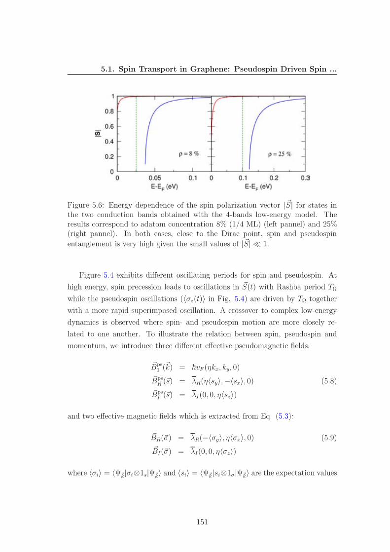
5.1. Spin Transport in Graphene: Pseudospin Driven Spin ...
Figure 5.6: Energy dependence of the spin polarization vector |~S| for states inthe two conduction bands obtained with the 4-bands low-energy model. Theresults correspond to adatom concentration 8% (1/4 ML) (left pannel) and 25%(right pannel). In both cases, close to the Dirac point, spin and pseudospin
entanglement is very high given the small values of |~S| ≪ 1.
Figure 5.4 exhibits different oscillating periods for spin and pseudospin. At
high energy, spin precession leads to oscillations in ~S(t) with Rashba period TΩ
while the pseudospin oscillations (〈σz(t)〉 in Fig. 5.4) are driven by TΩ together
with a more rapid superimposed oscillation. A crossover to complex low-energy
dynamics is observed where spin- and pseudospin motion are more closely re-
lated to one another. To illustrate the relation between spin, pseudospin and
momentum, we introduce three different effective pseudomagnetic fields:
~Bps0 (~k) = ~vF (ηkx, ky, 0)
~BpsR (~s) = λR(η〈sy〉,−〈sx〉, 0) (5.8)
~BpsI (~s) = λI(0, 0, η〈sz〉)
and two effective magnetic fields which is extracted from Eq. (5.3):
~BR(~σ) = λR(−〈σy〉, η〈σx〉, 0) (5.9)
~BI(~σ) = λI(0, 0, η〈σz〉)
where 〈σi〉 = 〈Ψ~k|σi⊗1s|Ψ~k〉 and 〈si〉 = 〈Ψ~k|si⊗1σ|Ψ~k〉 are the expectation values
151
5.1. Spin Transport in Graphene: Pseudospin Driven Spin ...
of the pseudospin and spin operators, σi and si (analogous to decoupled subsys-
tems), and Ψ~k are the eigenstates of the KMR Hamiltonian (see Eq. ((5.5))).
From the form of the effective magnetic fields, it is seen that unlike the case of
semiconductors where SOC directly couples spin with momentum, in graphene
spin couples directly with pseudospin (see BR and BpsR ), and is related to momen-
tum via the coupling between pseudospin and momentum h0(~k), a term which
vanishes at the Dirac point. These effective magnetic fields help illustrating the
energy crossover in Fig. 5.4.
While the occurrence of the same Rashba precession for spin and pseudospin
at high energy (Fig. 5.4 a) is related to the analogy of the effective fields (BR
for spin and BpsR for pseudospin), the superimposed rapid oscillation in σz can
be rationalized as follows. We observe that at high energy the nearest neighbor
hopping from three neighbors, h0 ∝ k, dictates additional pseudospin precession
about a radial in-plane field B ps0 (∝ k) = hvF (kx, ky, 0) with small amplitudes for
〈σz(t)〉 and with a period given by T ps0 = π~/E (0.016ps for E = 130 meV).
For the overall dynamics it is important that this rapid pseudospin precession
about B ps0 does not affect the slower spin dynamics imposed by hR. Indeed we
can replace σx by its time average 〈σx〉 and σy → 〈σy〉 in BR. As a result, there
is only weak interference (feedback) between spin and pseudospin dynamics and
both degrees of freedom can be understood as being driven independently by
their respective effective fields.
In contrast, at low energy, the above replacements are no longer justified and
BR becomes time dependent through the time dependence of 〈~σ〉 (analogously
for BpsR and 〈~s〉) resulting in complex spin-pseudospin dynamics with new char-
acteristic periods.
Momentum relaxation, spin relaxation and entanglement of states in gold-
decorated graphene samples
From the analysis of spin dynamics using the microscopic and continuum mod-
els ( Fig. 5.3 and Fig. 5.4), we have shown that the spin relaxation mechanism
close to the Dirac point is inconsistent with Elliot-Yafet (EY) or Dyakonov-Perel
(DP) scaling laws. For EY, the spin relaxation time is proportional to the mo-
mentum relaxation time as τEYs ≈ Ncollisions · τp, where Ncollisions ≫ 1 denotes
the number of scattering-off-impurity events before spin flip occurs and τp is the
152
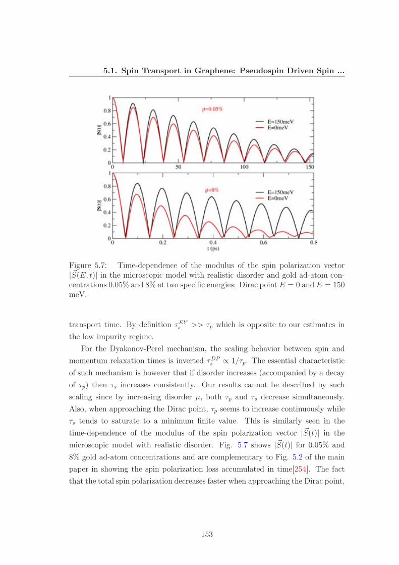
5.1. Spin Transport in Graphene: Pseudospin Driven Spin ...
Figure 5.7: Time-dependence of the modulus of the spin polarization vector|~S(E, t)| in the microscopic model with realistic disorder and gold ad-atom con-centrations 0.05% and 8% at two specific energies: Dirac point E = 0 and E = 150meV.
transport time. By definition τEYs >> τp which is opposite to our estimates in
the low impurity regime.
For the Dyakonov-Perel mechanism, the scaling behavior between spin and
momentum relaxation times is inverted τDPs ∝ 1/τp. The essential characteristic
of such mechanism is however that if disorder increases (accompanied by a decay
of τp) then τs increases consistently. Our results cannot be described by such
scaling since by increasing disorder µ, both τp and τs decrease simultaneously.
Also, when approaching the Dirac point, τp seems to increase continuously while
τs tends to saturate to a minimum finite value. This is similarly seen in the
time-dependence of the modulus of the spin polarization vector |~S(t)| in the
microscopic model with realistic disorder. Fig. 5.7 shows |~S(t)| for 0.05% and
8% gold ad-atom concentrations and are complementary to Fig. 5.2 of the main
paper in showing the spin polarization loss accumulated in time[254]. The fact
that the total spin polarization decreases faster when approaching the Dirac point,
153
5.1. Spin Transport in Graphene: Pseudospin Driven Spin ...
where momentum relaxation time (τp) is larger, is a further confirmation of our
interpretation that spin-pseudospin entanglement driven by Rashba-type spin-
orbit coupling is at the heart of the spin relaxation mechanism of gold-decorated
graphene at low energies.
Influence of charge puddles.
It is well known that charge puddles in graphene can make the Dirac point
energy fluctuating due to local changes in the chemical potential [255] possi-
bly hindering the observation of the discussed spin-relaxation mechanism at low
energy. As recently reported by Xue et al. [256], the fluctuation (standard de-
viation) of the Dirac point energy in supported graphene samples depends on
the substrate and range from ∆E ≈ 56 meV for SiO2 to ∆E ≈ 5 meV for hBN
[256] in consistency with a previous paper reporting 50 meV for SiO2 [197]. The
difference in the energetic position of the Dirac point is intimately related to the
size of the charge puddles induced by the substrate which reach an approximate
size of 10 nm for SiO2 and around 100 nm for hBN. By comparing the rele-
vant energies for the band onsets (i.e. energies where |~S| ≪ 1) in Fig. 5.6 and
the Fermi energy fluctuations from literature, we expect that the spin relaxation
mechanism proposed in this manuscript, based on spin-pseudospin entanglement,
should be experimentally accessible.
Analogy to spin-less bilayer graphene We observe that the Hamiltonian in
Eq.((5.3)) is very similar to the one of spin-less bilayer graphene (BLG) at low
energies and shows a very similar band dispersion around both valleys [257, 258,
259], although the nature of eigenstates is quite different [84]. Below we compare
the Hamiltonian matrices of both cases. The KMR Hamiltonian in one valley
reads
H(K)KMR =
λI v(kx − iky) 0 0
v(kx + iky) −λI −2iλR 0
0 2iλR −λI v(kx − iky)
0 0 v(kx + iky) λI
(5.10)
and the spin-less BLG-Hamiltonian, in its most reduced version [259], can be
154
5.1. Spin Transport in Graphene: Pseudospin Driven Spin ...
expressed as:
H(K)BLG =
−∆′ v(kx − iky) 0 0
v(kx + iky) ∆′ γ1 0
0 γ1 ∆′ v(kx − iky)
0 0 v(kx + iky) −∆′
(5.11)
where γ1 is the interlayer hopping which connects a B-site in the top layer with
an A-site in the bottom layer in Bernal stacked bilayer graphene. This interaction
induces a staggered potential ±∆′ within each layer distinguishing carbon atoms
in top position and those at hollow-sites. Interestingly, this staggered potential
changes sign at opposite layers similarly to the intrinsic spin-orbit coupling λI in
graphene.
It is helpful to write the above Hamiltonian in terms of Pauli matrices in order
to compare with Eqs. (5.3):
hBLG0 (~k) = ~vF (ησxkx + σyky) ⊗ 1s
hBLGγ (~k) = γ1 ([σx ⊗ ξx] + [σy ⊗ ξy])
hBLG∆ (~k) = ∆′ [σz ⊗ ξz] (5.12)
where the layer operator ~ξ in Eq.((5.12)) plays the role of the spin operator ~s
in Eq.((5.3)), while the second degree of freedom is the pseudospin ~σ in both
cases. It is important to note that, while the first and third terms in Eq.((5.12))
resemble the ones in Eq.((5.3)), the second one has a different structure in terms
of Pauli matrices when compared to the Rashba term. However, it also leads to
in-plane effective pseudomagnetic and magnetic fields of the form:
~Bpsγ (~ξ) = γ1(〈ξx〉, 〈ξy〉, 0) (5.13)
~Bγ(~σ) = γ1(〈σx〉, 〈σy〉, 0). (5.14)
Also, the eigenstates of the BLG Hamiltonian, while no longer complex, still
show a layer-pseudospin entanglement at low-energies allowing for new interesting
155
5.1. Spin Transport in Graphene: Pseudospin Driven Spin ...
phenomena regarding layer relaxation in Bernal stacked bilayer graphene
ΨBLG,I~k,±
=
(
0
1
)
⊗ |1〉 ±(
1
0
)
⊗ |2〉 (5.15)
ΨBLG,II~k,±
=
(
1
0
)
⊗ |1〉 ±(
0
1
)
⊗ |2〉. (5.16)
The apparent similarity of both Hamiltonians indicates the possibility to ob-
serve physical effects similar to the presently studied spin relaxation and spin-
pseudospin entanglement when considering ’layer-polarized’ carrier transport in
graphene. It would be interesting to study the effect of layer-pseudospin entan-
glement in such a situation.
In conclusion, our spin transport simulations in graphene, chemically mod-
ified by a random distribution of ad-atoms, have revealed a hitherto unknown
phenomenon related to the entangled dynamics of spin and pseudospin, which is
induced by spin-orbit coupling and leads to fast spin relaxation in a quasi-ballistic
transport regime. The entanglement between spin and orbital degrees of freedom
has been discussed for models of ballistic semiconducting nanowires [254]. Here,
the energy-dependence of spin/pseudospin entanglement induced by spin-orbit
coupling has been shown to directly impact the resulting spin dynamics and spin
relaxation times. Faster spin relaxation develops when spin-pseudospin entan-
glement is maximized at the Dirac point, where the momentum scattering time
becomes increasingly large because disorder preserves pseudospin symmetry.
This relaxation mechanism, occurring in clean graphene with long mean free
paths, has no equivalent in condensed matter and cannot be described by EY
or DP scaling. Such a phenomenon is here revealed for the specific case of gold
adsorbates, but should also be at play for other sources of local spin-orbit coupling
(ripples, defects, etc.), thus contributing to a deep general understanding of spin
transport in graphene-based materials and devices [44, 45, 46, 47, 48], while
the specific spin relaxation time depends on the effective strength of the SOC
being different for different sources. The effect of lateral confinement in stripe
or ribbon geometry deserves further investigation regarding its influence on spin
relaxation (which was observed in semiconductor nanowires [260]), while some
156
5.2. Quantum Spin Hall Effect
general mechanism due to flexural phonons for spin relaxation in 2D membranes
has been proposed. [261]
Finally, the spin-pseudospin entanglement could open the path to control
the pseudospin by modifying the spin or vice versa. For example, spins could
be manipulated by inducing pseudomagnetic fields by straining graphene. Such
possibilities could lead to the development of novel approaches for non-charge-
based information processing and computing, resulting in a new generation of ac-
tive (CMOS-compatible) spintronic devices together with non-volatile low-energy
MRAM memories [262].
5.2 Quantum Spin Hall Effect
5.2.1 Introduction
In 2005, Kane and Mele predicted the existence of the Quantum Spin Hall Ef-
fect (QSHE) in graphene due to intrinsic spin-orbit coupling [51, 263]. Within
the QSHE, the presence of spin-orbit coupling, which can be understood as a
momentum-dependent magnetic field coupling to the spin of the electron, results
in the formation of chiral (anti-chiral) integer quantum Hall Effect for spin up
(spin down) electron population. The observation of QSHE has been however
prohibited in clean graphene by the vanishingly small intrinsic spin-orbit cou-
pling in the order of µeV [85], but further realized in strong SOC materials (such
as CdTe/HgTe/CdTe quantum wells or bismuth selenide and telluride alloys),
giving rise to the new exciting field of topological insulators [264, 265, 266, 267].
Recent proposals to induce a topological phase in graphene include functionaliza-
tion with heavy adatoms [29, 268], covalent functionalization of the edges [269],
proximity effect with other topological insulators [270, 271, 272], or intercala-
tion and functionalization with 5d transition metals [273, 274]. In particular,
the seminal theoretical study [29] by Weeks and co-workers has revealed that
graphene endowed with modest coverage of heavy adatoms (such as indium and
thallium) could exhibit a substantial band gap and QSHE fingerprints (detectable
in transport or spectroscopic measurements). For instance, signature of such a
topological state could be seen in a robust quantized two-terminal conductance
157
5.2. Quantum Spin Hall Effect
(2e2/h), with an adatom density dependent conductance plateau extending inside
the bulk gap induced by SOC [29, 275, 276]. To date, such a prediction lacks
experimental confirmation, despite some recent results on indium-functionalized
graphene have shown a surprising reduction of the Dirac point resistance with
increasing indium density [277]. On the other hand, it is known that adatoms
deposited on graphene will inevitably segregate, forming islands rather than a
homogeneous distribution [278]. Such a clustering effect may seriously impact on
the transport features [279, 280, 281].
In this Letter, we show that the clustering of thallium adatoms on graphene
could suppress the formation of a quantum spin-Hall phase, while the resulting
functionalized structures would exhibit unconventional bulk transport character-
istics, with absence of transition to an insulating regime and a robust Dirac point
conductivity close to 4e2/h. The presence of adatom islands locally introduc-
ing strong spin-orbit coupling is actually found to prevent the development of
quantum interferences and localization phenomena induced by additional strong
disorder sources.
5.2.2 Adatom Clustering Effect on QSHE
Model and Methods.– When a thallium atom is grafted on graphene, it places in
the middle of a hexagonal plaquette of carbon atoms, above the surface, see Fig
5.8. As shown in [29], the degrees of freedom corresponding to the adatom can
be conveniently decimated and their effect included into an effective π-π* orthog-
onal tight-binding model with spin-orbit coupling. In the presence of adatoms
randomly distributed over a set R of plaquettes, the Hamiltonian [51, 263] reads
as
H = − γ0∑
〈ij〉
c†icj +2i√
3λ∑
〈〈ij〉〉∈R
c†i~s · (~dkj × ~dik)cj
− µ∑
i∈R
c†ici +∑
i
Vic†ici , (5.17)
where ci = [ci↓, ci↑] is the couple of annihilation operators for electrons with
spin down and spin up on the ith carbon atom, and c†i is the corresponding
158
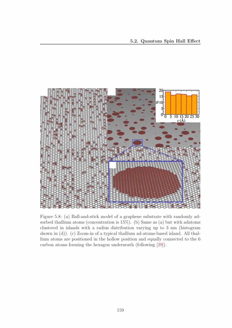
5.2. Quantum Spin Hall Effect
Figure 5.8: (a) Ball-and-stick model of a graphene substrate with randomly ad-sorbed thallium atoms (concentration is 15%). (b) Same as (a) but with adatomsclustered in islands with a radius distribution varying up to 3 nm (histogramshown in (d)). (c) Zoom-in of a typical thallium ad-atoms-based island. All thal-lium atoms are positioned in the hollow position and equally connected to the 6carbon atoms forming the hexagon underneath (following [29]).
159
5.2. Quantum Spin Hall Effect
couple of creation operators. The first contribution in Eq.(5.17) is the nearest
neighbor hopping tight-binding term, with coupling energy γ0 = 2.7 eV. The
second contribution is a next nearest neighbor hopping term that represents the
SOC induced by the adatoms, with ~dkj and ~dik the unit vectors along the two
bonds connecting second neighbors and ~s the spin Pauli matrices. The SOC is
set to λ = 0.02γ0, as extracted from ab-initio simulations in Ref. [29]. The third
term describes the potential energy induced by charge transfer between adatoms
and graphene. The last term represents the long-range interaction of graphene
and impurities in the substrate Vi =∑N
j=1 ǫj exp[−(ri −Rj)2/(2ξ2)] [137], where
ξ = 0.426 nm is the effective range and the sum runs over N impurity centers with
random positions Rj and magnitude of the potential ǫj randomly chosen within
[−∆,∆]. The Hamiltonian does not consider the effect of a further structure
relaxation in the case of clustered adatoms. This will not alter our conclusions.
For the study of electronic transport in thallium-functionalized ribbons, we
consider a standard two-terminal configuration with highly doped contacts. The
doping is mimicked by an appropriate potential energy V on source and drain.
The simulations are based on the nonequilibrium Green’s function formalism
[282]. In addition to the electronic conductance, this approach provides us with
the spin-resolved local density-of-occupied-states. This quantity illustrates how
electrons injected from the source spatially distribute in the system depending
on their spin. More specifically, the zero-temperature differential conductance as
a function of the electron energy is obtained by the Landauer-Buttiker formula
G(E) = (e2/h)Tr[GR(E)Γ(S)GA(E)Γ(D)] , (5.18)
where GR/A are the retarded and advanced Green’s functions and Γ(S/D) are the
rate operators for the source and drain contacts. The local density-of-occupied-
states is obtained as
ρiη(E) = ℑm[G<(E)]iη,iη/(2π) (5.19)
where [G<]iη,iη is the diagonal element of the lesser Green’s function corresponding
to the electron with spin η (↓, ↑) of the ith carbon atom, and ℑm indicates the
imaginary part.
We also study quantum transport in two-dimensional functionalized graphene
160
5.2. Quantum Spin Hall Effect
by means of the Kubo approach [1, 4]. The scaling properties of the conductivity
can be followed through the dynamics of electronic wavepackets using Eq. (3.41).
Calculations, based on the use of Chebyshev polynomial expansion and contin-
ued fractions, are performed on systems containing more than 3.5 million carbon
atoms, which corresponds to sizes larger than 300 × 300 nm2. Such a size guar-
antees that our results are weakly dependent on the specific spatial distribution
of adatoms or clusters of adatoms.
Suppression of QSHE by adatom clustering.– We start by considering an arm-
chair ribbon of width W=50 nm functionalized with a concentration n=15% of
randomly scattered thallium adatoms over a length L=50 nm. As already re-
ported in the literature [29], the differential conductance [continuous line in Fig.
5.9(a)] clearly shows a 2e2/h plateau, which is signature of quantum spin-Hall
phase. Note that the plateau is centered at E ≈-120 meV and has an extension of
about 100 meV. The observed charge neutrality point shift is consistent with the
concentration of carbon atoms ∼ 3n that undergo a charge transfer doping effect,
i.e. E ≈ −3nµ =-121.5 meV. The width of the plateau approximately corre-
sponds to the topological gap induced by thallium functionalization, and is given
by 6√
3λeff ≈84.2 meV, where the effective SOC is λeff = nλ ≈8.1 meV [283]. A
closer inspection of the conductance shows that actually the plateau region is not
perfectly flat, but varies within the range [1.92,2.02] e2/h. This indicates that the
separation between spin polarized chiral edge channels is not complete. A better
quantization may be achieved by increasing W , L or the adatom concentration.
Figures 5.9(b,c) also show the spin resolved local density-of-occupied-states ρ for
electrons injected from the right contact at energy E = −100 meV, indicated by
an arrow in Fig. 5.9(a). We observe a high ρ for x > 50 nm, i.e. the region of the
source (injected electrons are indicated by arrows), and spin-polarized channels
along the upper edge for spin down (b) and along the lower edge for spin up (c).
The width of the polarized edge channels in armchair ribbons does not depend
on the energy but only on the SOC as aγ0/(2√
3λeff) ≈13.5 nm (see [284]). The
separation between the right-to-left and left-to-right moving channels, which is
opposite for different spin polarizations, is at the origin of the QSHE. To test its
robustness, we consider the presence of a concentration nLR = 0.5% of long-range
disorder with different strength ∆. As reported in Fig. 5.9(a), a plateau, though
161
5.2. Quantum Spin Hall Effect
narrower, is observed up to ∆=1 eV.
This picture is actually strongly modified when adatoms segregate and form
islands. Figure 5.10(a) shows the evolution of the differential conductance when
islands have a radius r varying from 0 (non-segregated case) to 1 nm and finally
to random values between 2 and 3 nm. The adatom concentration is kept at
n = 15%. While a signature of the plateau remains up to r = 1, for larger ra-
dius the quantization is completely lost despite the short intercluster distance.
This indicates that segregation has a detrimental effect on the formation of a
QSH phase in graphene by heavy adatom functionalization. Considering that
adatom clustering is unavoidable at room temperature, our findings provide an
explanation for the missing experimental observation of the QSHE in such sys-
tems. A deeper insight into the effect of segregation is further provided by the
spin-resolved density-of-occupied-states reported in Figs.5.10(b,c) for the case of
island radii in the range [2,3] nm. The ρ distribution is very similar for spin down
and spin up electrons, this means that most of the spin-coupling related effect is
suppressed. Moreover, the injected electrons largely spread all over the ribbon
and show a higher concentration inside the islands. To explain these features, we
have to consider that segregation reduces the homogeneous coverage of adatoms
and leaves large regions of pristine graphene. As a consequence, the topological
gap cannot develop in these regions, where electrons flow the same way as in
non-topological systems. Moreover, the clusters are too small and the SOC is too
weak to induce a topological phase inside them. Together with the highly negative
value of the charge neutrality point inside the islands (E = 3µ =-810 meV), this
determines the considerably high electron density observed in the figure. How-
ever, as shown below, clustering of thallium adatoms produces a remarkable bulk
transport fingerprint of the spin-orbit coupling in two-dimensional graphene.
Robust metallic state and minimum conductivity.– We investigate the intrinsic
bulk conductivity of thallium-functionalized graphene by computing the Kubo-
Greenwood conductivity. We focus on large thallium density (about 15%), with
thallium clusters size distribution shown in Fig. 5.8 (d) and consider superim-
posed distribution of long-range impurities to mimic additional sources of disor-
der (such as charged defects trapped in the underneath oxide, additional dopants,
structural defects...). In Fig. 5.11 (main frame), we show the Kubo conductivity
162
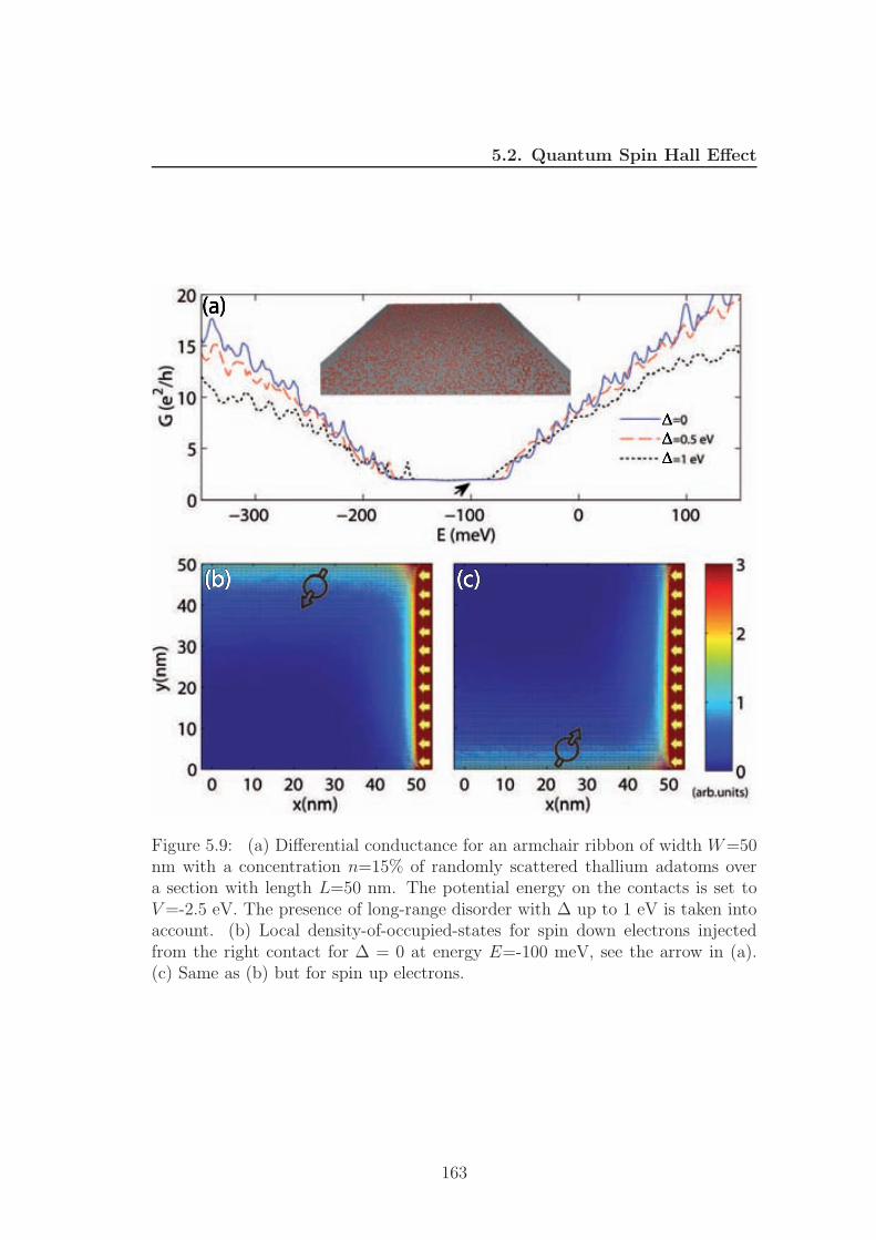
5.2. Quantum Spin Hall Effect
Figure 5.9: (a) Differential conductance for an armchair ribbon of width W=50nm with a concentration n=15% of randomly scattered thallium adatoms overa section with length L=50 nm. The potential energy on the contacts is set toV=-2.5 eV. The presence of long-range disorder with ∆ up to 1 eV is taken intoaccount. (b) Local density-of-occupied-states for spin down electrons injectedfrom the right contact for ∆ = 0 at energy E=-100 meV, see the arrow in (a).(c) Same as (b) but for spin up electrons.
163
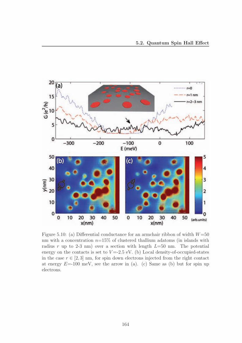
5.2. Quantum Spin Hall Effect
Figure 5.10: (a) Differential conductance for an armchair ribbon of width W=50nm with a concentration n=15% of clustered thallium adatoms (in islands withradius r up to 2-3 nm) over a section with length L=50 nm. The potentialenergy on the contacts is set to V=-2.5 eV. (b) Local density-of-occupied-statesin the case r ∈ [2, 3] nm, for spin down electrons injected from the right contactat energy E=-100 meV, see the arrow in (a). (c) Same as (b) but for spin upelectrons.
164
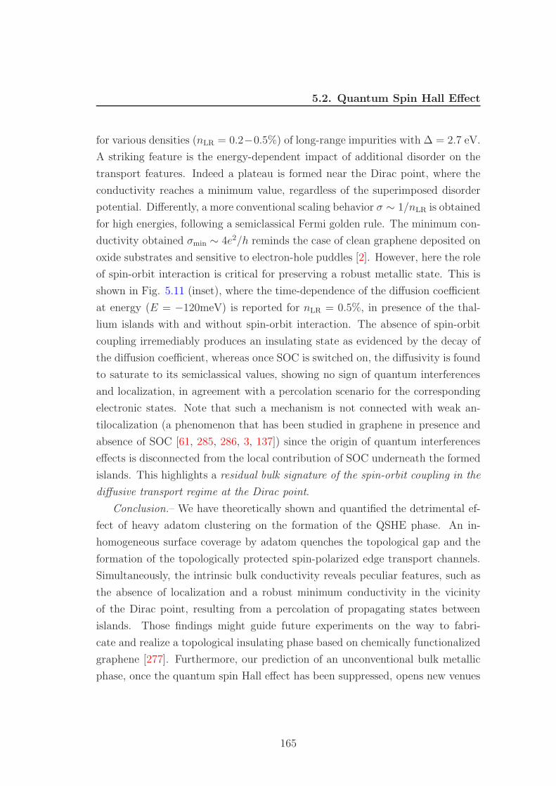
5.2. Quantum Spin Hall Effect
for various densities (nLR = 0.2−0.5%) of long-range impurities with ∆ = 2.7 eV.
A striking feature is the energy-dependent impact of additional disorder on the
transport features. Indeed a plateau is formed near the Dirac point, where the
conductivity reaches a minimum value, regardless of the superimposed disorder
potential. Differently, a more conventional scaling behavior σ ∼ 1/nLR is obtained
for high energies, following a semiclassical Fermi golden rule. The minimum con-
ductivity obtained σmin ∼ 4e2/h reminds the case of clean graphene deposited on
oxide substrates and sensitive to electron-hole puddles [2]. However, here the role
of spin-orbit interaction is critical for preserving a robust metallic state. This is
shown in Fig. 5.11 (inset), where the time-dependence of the diffusion coefficient
at energy (E = −120meV) is reported for nLR = 0.5%, in presence of the thal-
lium islands with and without spin-orbit interaction. The absence of spin-orbit
coupling irremediably produces an insulating state as evidenced by the decay of
the diffusion coefficient, whereas once SOC is switched on, the diffusivity is found
to saturate to its semiclassical values, showing no sign of quantum interferences
and localization, in agreement with a percolation scenario for the corresponding
electronic states. Note that such a mechanism is not connected with weak an-
tilocalization (a phenomenon that has been studied in graphene in presence and
absence of SOC [61, 285, 286, 3, 137]) since the origin of quantum interferences
effects is disconnected from the local contribution of SOC underneath the formed
islands. This highlights a residual bulk signature of the spin-orbit coupling in the
diffusive transport regime at the Dirac point.
Conclusion.– We have theoretically shown and quantified the detrimental ef-
fect of heavy adatom clustering on the formation of the QSHE phase. An in-
homogeneous surface coverage by adatom quenches the topological gap and the
formation of the topologically protected spin-polarized edge transport channels.
Simultaneously, the intrinsic bulk conductivity reveals peculiar features, such as
the absence of localization and a robust minimum conductivity in the vicinity
of the Dirac point, resulting from a percolation of propagating states between
islands. Those findings might guide future experiments on the way to fabri-
cate and realize a topological insulating phase based on chemically functionalized
graphene [277]. Furthermore, our prediction of an unconventional bulk metallic
phase, once the quantum spin Hall effect has been suppressed, opens new venues
165
5.2. Quantum Spin Hall Effect
Figure 5.11: Kubo conductivity versus energy for thallium clustering and addi-tional varying density (nLR) of long-range impurities. Inset: Diffusion coefficientfor wavepacket with energy E=-120meV, for the case nLR = 0.5%, with (solidblue line) and without the spin-orbit coupling of thallium adatoms activated.
166
5.2. Quantum Spin Hall Effect
for exploring new and original spin-orbit related quantum transport phenomena
in graphene/topological-insulator hybrid systems [272]. In the same perspec-
tive, it would be interesting to study the formation and robustness of a quantum
anomalous Hall phase in presence of segregation of 3d transition metallic adatoms
on graphene [275, 287].
167
Chapter 6
Conclusions
In this thesis, I have presented the charge transport of disordered graphene as
well as explained the fast spin relaxation in graphene which is one of the most
interesting topics in graphene at the moment.
The role of defect-induced zero-energy modes on charge transport in graphene
is investigated using Kubo and Landauer transport calculations. By tuning the
density of random distributions of monovacancies either equally populating the
two sublattices or exclusively located on a single sublattice, all conduction regimes
are covered from direct tunneling through evanescent modes to mesoscopic trans-
port in bulk disordered graphene. Depending on the transport measurement
geometry, defect density, and broken sublattice symmetry, the Dirac-point con-
ductivity is either exceptionally robust against disorder (supermetallic state) or
suppressed through a gap opening or by algebraic localization of zero-energy
modes, whereas weak localization and the Anderson insulating regime are ob-
tained for higher energies. These findings clarify the contribution of zero-energy
modes to transport at the Dirac point, hitherto controversial.
We also reported new insights to the current understanding of charge trans-
port in intrinsic polycrystalline geometries. We created realistic models of large
CVD-grown graphene samples and then computed the corresponding charge car-
rier mobilities as a function of the average grain size and the coalescence quality
between the grains. Our results reveal a remarkably simple scaling law for the
mean free path and conductivity, correlated to atomic-scale charge density fluc-
tuations along grain boundaries.
168
6. Conclusions
Furthermore, we used numerical simulations and transport measurements to
demonstrate that electrical properties and chemical modification of graphene
grain boundaries are strongly correlated. This not only provides guidelines for the
improvement of graphene devices, but also opens a new research area of engineer-
ing graphene grain boundaries for highly sensitive electro-biochemical devices.
We investigated the charge transport properties of planar amorphous graphene
that is fully topologically disordered, in the form of sp2 threefold coordinated net-
works consisting of hexagonal rings but also including many pentagons and hep-
tagons distributed in a random fashion. Using the Kubo transport methodology
and the Lanczos method, the density of states, mean free paths, and semiclassical
conductivities of such amorphous graphene membranes are computed. Despite
a large increase in the density of states close to the charge neutrality point, all
electronic properties are dramatically degraded, evidencing an Anderson insulat-
ing state caused by topological disorder alone. These results are supported by
Landauer-Buttiker conductance calculations, which show a localization length as
short as 5nm.
We reported on the transition from a Quantum Spin Hall effect (QSHE)
regime to a robust metallic state, upon segregation of thallium adatoms ad-
sorbed onto a graphene surface and introducing giant enhancement of spin-
orbit coupling. Our theoretical methodology combines efficient calculation of
both the Landauer-Buttiker conductance and the Kubo-Greenwood conductiv-
ity, giving access to both edge and bulk transport physics in disordered thallium-
functionalized graphene systems of realistic sizes. Our findings quantify the detri-
mental effects of adatoms clustering in observing the QSHE, but provide addi-
tional bulk signature of a robust metallic state with minimum bulk conductivity
of about 4e2/h, which should be helpful for guiding further experiments.
Finally, we have developed a new spin-transport-simulation method to inves-
tigate the spin transport in graphene. We showed that the presence of a low
density of randomly distributed adatoms (inducing local Rashba spin-orbit cou-
pling) yields ultrafast spin relaxation times at the Dirac point, together with an
unconventional relation between the spin and momentum relaxation times. Our
quantum transport simulations showed that certain types of adatoms (such as
Nickel or Gold impurities) trigger strong spin decoherence at the Dirac point,
169
6. Conclusions
although the transport regime eventually reaches the ballistic limit. This phe-
nomenon hitherto unknown is a new type of spin dephasing mechanism, driven
by entanglement between spin and pseudospin degrees of freedom. Those find-
ings bring an unprecedented insight of spin relaxation mechanisms in graphene,
suggesting a possible origin of reported low spin relaxation times, and clarifica-
tion of the controversial description of relaxation mechanisms in various types of
graphene samples.
170
List of Publications
1. Aron W. Cummings, Dinh Loc Duong, Van Luan Nguyen, Dinh Van
Tuan, Jani Kotakoski, Jose Eduardo Barrios Vargas, Young Hee Lee and
Stephan Roche. Charge Transport in Polycrystalline Graphene: Challenges
and Opportunities. Advanced Materials (2014)
2. David Jimenez, Aron W. Cummings, Ferney Chaves, Dinh Van Tuan,
Jani Kotakoski, and Stephan Roche. Impact of graphene polycrystallinity
on the performance of graphene field-effect transistors. Appl. Phys. Lett.,
104, 043509 (2014)
3. Dinh Van Tuan, Jani Kotakoski, Thibaud Louvet, Frank Ortmann, Jan-
nik C. Meyer, and Stephan Roche. Scaling Properties of Charge Transport
in Polycrystalline Graphene. Nano Letters, 13 (4), 1730–1735 (2013)
4. Alessandro Cresti, Frank Ortmann, Thibaud Louvet, Dinh Van Tuan, and
Stephan Roche. Broken Symmetries, Zero-Energy Modes, and Quantum
Transport in Disordered Graphene. Phys. Rev. Lett., 110, 196601 (2013).
5. Alessandro Cresti, Thibaud Louvet, Frank Ortmann , Dinh Van Tuan ,
Pawe l Lenarczyk , Georg Huhs and Stephan Roche. Impact of Vacancies on
Diffusive and Pseudodiffusive Electronic Transport in Graphene. Crystals,
3, 289–305 (2013).
6. Dinh Van Tuan, Avishek Kumar, Stephan Roche, Frank Ortmann, M. F.
Thorpe, and Pablo Ordejon. Insulating behavior of an amorphous graphene
membrane. Phys. Rev. B, 86, 121408 (Rapid Communications) (2012)
171
List of Publications
7. Dinh Van Tuan, Frank Ortmann , David Soriano, Sergio O. Valenzuela,
and Stephan Roche. Spin transport in graphene: pseudospin driven spin
relaxation mechanism. Nature Physics (submitted)
8. Alessandro Cresti, David Soriano, Dinh Van Tuan, Aron W. Cummings,
and Stephan Roche. Heavy Atom Clustering in Graphene: Crossover be-
tween Quantum Spin Hall Effect and Bulk Minimum Conductivity. Physical
Review Letter (submitted)
172
Appendix A: Time Evolution Of
The Wave Packet
This appendix presents how to calculate the evolution of the wave packet U(t)|ϕRP 〉and [X, U(t)]|ϕRP 〉 which are used in the application of the real space method to
calculate the transport properties. In order to do that, we divide the time t into
small time steps T = t/N and approximate U(T ) with the series of orthogonal
Chebyshev polynomials Qn(H)
U(T ) = e−iHT
~ =
∞∑
n=0
cn(T )Qn(H) (1)
The original Chebyshev polynomials Tn which satisfy the recurrent relations
T0(x) = 1 (2)
T1(x) = x (3)
T2(x) = 2x2 − 1 (4)...
Tn+1(x) = 2x Tn(x) − Tn−1(x) (5)
and act on the interval [−1; 1] are rescaled to the rescaled Chebyshev polynomials
Qn which cover the bandwidth of system Hamiltonian E ∈ [a−2b : a+2b], with the
173
Appendix A: Time Evolution Of The Wave Packet
band center and bandwidth are a and 4b, respectively. These rescaled Chebyshev
polynomials Qn sastify
Qn(E) =√
2Tn
(
E − a
2b
)
(∀n ≥ 1) (6)
Q0(E) = 1 (7)
Q1(E) =√
2E − a
2b(8)
Q2(E) = 2√
2
(
E − a
2b
)2
−√
2 (9)
...
Qn+1(E) = 2
(
E − a
2b
)
Qn(E) −Qn−1(E) (10)
With above definition, we have the orthonormal relations for Qn(E)
∫
Qn(E)Qm(E)pQ(E)dE = δmn (11)
with respect to the weight
pQ(E) =1
2πb√
1 −(
E−a2b
)2(12)
Once the Qn polynomials are well defined, one can compute the related cn(T )
coefficients
cn(T ) =
∫
dE pQ(E)Qn(E)e−iE~T (13)
=
∫
dE
√2Tn
(
E−a2b
)
2πb√
1 −(
E−a2b
)2e−iE
~T (14)
=
√2
π
∫ 1
−1
dxTn(x)√1 − x2
e−i (2bx+a)~
T (15)
=√
2ine−ia~TJn
(
−2b
~T
)
, n ≥ 1 (16)
174
Appendix A: Time Evolution Of The Wave Packet
and the first coefficients c0(T ) = ine−ia~TJ0
(
−2b~T)
with Jn(x) is the Bessel func-
tion of the first kind and order n
We can now calculate |ϕRP (T )〉
|ϕRP (T )〉 = U(T )|ϕRP 〉 (17)
|ϕRP (T )〉 ≃N∑
n=0
cn(T )Qn(H)|ϕRP 〉 =N∑
n=0
cn(T )|αn〉 (18)
where |αn〉 = Qn(H)|ϕRP 〉. With the definitions introduced in Eq. (7,8 and 9)
and the recurrence relation Eq.(10), we obtain
|α0〉 = |ϕRP 〉 (19)
|α1〉 =
(
H − a√2b
)
|α0〉 (20)
|α2〉 =
(
H − a
b
)
|α1〉 −√
2|α0〉 (21)
|αn+1〉 =
(
H − a
b
)
|αn〉 − |αn−1〉 (∀n ≥ 2) (22)
Following the same reasoning as for |ϕRP (T )〉, |ϕ′RP (T )〉 can be evaluated first
writting
|ϕ′RP (T )〉 = [X, U(T )]|ϕRP 〉 (23)
|ϕ′RP (T )〉 ≃
N∑
n=0
cn(T )[X, Qn(H)]|ϕRP 〉 =N∑
n=0
cn(T )|βn〉 (24)
with |βn〉 = [X, Qn(H)]|ϕRP 〉. Using the Eq. (10) and Eq. (19-22), we obtain
175
Appendix A: Time Evolution Of The Wave Packet
the recurrence relation for |βn〉
|β0〉 = 0 (25)
|β1〉 =
[
X, H]
√2b
|ϕRP 〉 (26)
|βn+1〉 =
(
H − a
b
)
|βn〉 − |βn−1〉 +1
b[X, H ]|αn〉 (∀n ≥ 1) (27)
which contain |αn〉 and the commutator [X, H] determined by the hopings and
the distances between neighbours
[X, H] =
0. . . Hij∆Xij
. . .
Hji∆Xji. . .
0
(28)
where ∆Xij = (Xi −Xj) is the distance between orbitals |ϕi〉 and |ϕj〉.
176
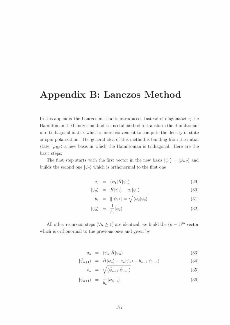
Appendix B: Lanczos Method
In this appendix the Lanczos method is introduced. Instead of diagonalizing the
Hamiltonian the Lanczos method is a useful method to transform the Hamiltonian
into tridiagonal matrix which is more convenient to compute the density of state
or spin polarization. The general idea of this method is building from the initial
state |ϕRP 〉 a new basis in which the Hamiltonian is tridiagonal. Here are the
basic steps:
The first step starts with the first vector in the new basis |ψ1〉 = |ϕRP 〉 and
builds the second one |ψ2〉 which is orthonormal to the first one
a1 = 〈ψ1|H|ψ1〉 (29)
|ψ2〉 = H|ψ1〉 − a1|ψ1〉 (30)
b1 = ‖|ψ2〉‖ =
√
〈ψ2|ψ2〉 (31)
|ψ2〉 =1
b1|ψ2〉 (32)
All other recursion steps (∀n ≥ 1) are identical, we build the (n+ 1)th vector
which is orthonormal to the previous ones and given by
an = 〈ψn|H|ψn〉 (33)
|ψn+1〉 = H|ψn〉 − an|ψn〉 − bn−1|ψn−1〉 (34)
bn =
√
〈ψn+1|ψn+1〉 (35)
|ψn+1〉 =1
bn|ψn+1〉 (36)
177
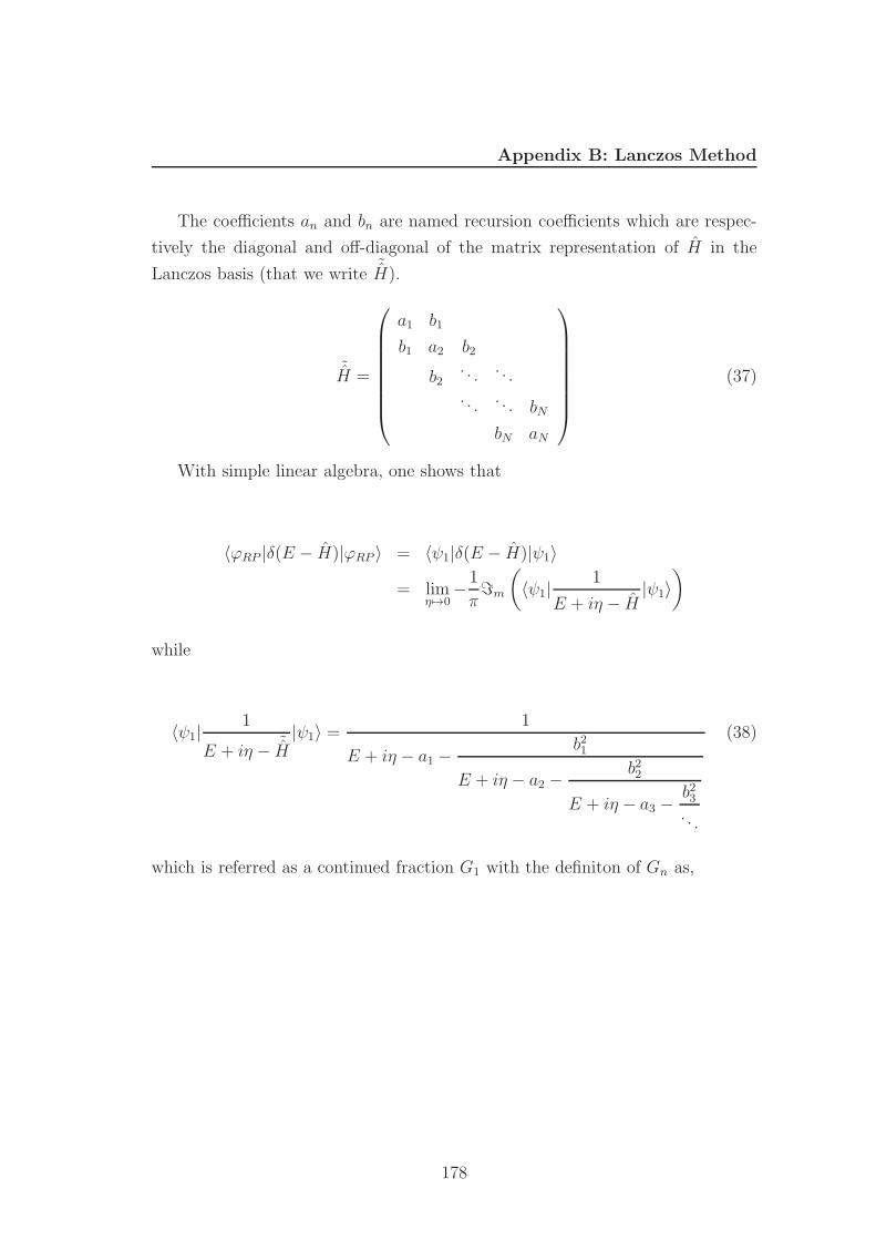
Appendix B: Lanczos Method
The coefficients an and bn are named recursion coefficients which are respec-
tively the diagonal and off-diagonal of the matrix representation of H in the
Lanczos basis (that we write˜H).
˜H =
a1 b1
b1 a2 b2
b2. . .
. . .. . .
. . . bN
bN aN
(37)
With simple linear algebra, one shows that
〈ϕRP |δ(E − H)|ϕRP 〉 = 〈ψ1|δ(E − H)|ψ1〉
= limη 7→0
−1
πℑm
(
〈ψ1|1
E + iη − H|ψ1〉
)
while
〈ψ1|1
E + iη − ˜H|ψ1〉 =
1
E + iη − a1 −b21
E + iη − a2 −b22
E + iη − a3 −b23. . .
(38)
which is referred as a continued fraction G1 with the definiton of Gn as,
178
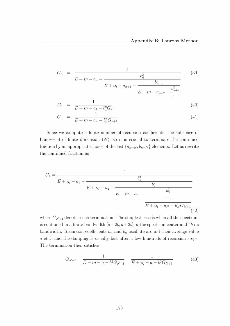
Appendix B: Lanczos Method
Gn =1
E + iη − an −b2n
E + iη − an+1 −b2n+1
E + iη − an+2 −b2n+2
. . .
(39)
G1 =1
E + iη − a1 − b21G2(40)
Gn =1
E + iη − an − b2nGn+1
(41)
Since we compute a finite number of recursion coefficients, the subspace of
Lanczos if of finite dimension (N), so it is crucial to terminate the continued
fraction by an appropriate choice of the last an=N , bn=N elements. Let us rewrite
the continued fraction as
G1 =1
E + iη − a1 −b21
E + iη − a2 −b22
E + iη − a3 −b23. . .
E + iη − aN − b2NGN+1
(42)
where GN+1 denotes such termination. The simplest case is when all the spectrum
is contained in a finite bandwidth [a−2b; a+2b], a the spectrum center and 4b its
bandwidth. Recursion coefficients an and bn oscillate around their average value
a et b, and the damping is usually fast after a few hundreds of recursion steps.
The termination then satisfies
GN+1 =1
E + iη − a− b2GN+2=
1
E + iη − a− b2GN+1(43)
179
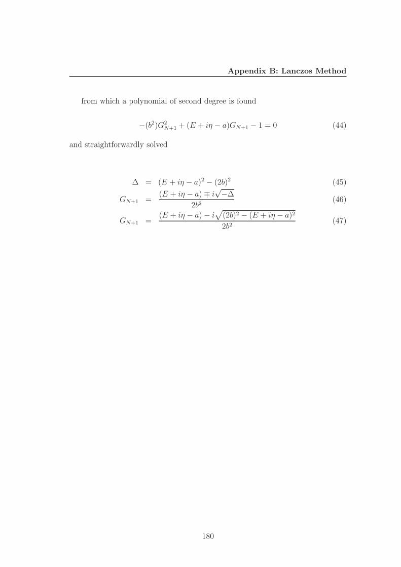
Appendix B: Lanczos Method
from which a polynomial of second degree is found
−(b2)G2N+1 + (E + iη − a)GN+1 − 1 = 0 (44)
and straightforwardly solved
∆ = (E + iη − a)2 − (2b)2 (45)
GN+1 =(E + iη − a) ∓ i
√−∆
2b2(46)
GN+1 =(E + iη − a) − i
√
(2b)2 − (E + iη − a)2
2b2(47)
180
References
[1] Luis E. F. Foa Torres, Stephan Roche, and Jean C. Charlier. Introduction
to Graphene-Based Nanomaterials From Electronic Structure to Quantum
Transport. Cambridge, 2013. viii, 7, 8, 45, 51, 53, 112, 161
[2] S. D. Sarma, S. Adam, E. H. Hwang, and E. Rossi. Rev. Mod. Phys., 83:407,
2011. viii, 10, 41, 63, 64, 78, 126, 165
[3] Y.Y. Zhang, J. Hu, B.A. Bernevig, X.R. Wan, X.C. Xie, and W.M. Liu.
Phys. Rev. Lett., 102:106401, 2009. viii, 15, 17, 165
[4] Stephan Roche, Nicolas Leconte, Frank Ortmann, Aurelien Lherbier, David
Soriano, and Jean-Christophe Charlier. Solid State Communications,
152:1404–1410, 2012. viii, 2, 16, 17, 18, 19, 66, 68, 94, 117, 126, 143,
161
[5] Frantisek Karlicky, Radek Zboil, and Michal Otyepka. J. Chem. Phys.,
137:034709, 2012. viii, 17
[6] Florian Banhart, Jani Kotakoski, and Arkady V. Krasheninnikov. ACS
nano, 5:26–41, 2011. viii, 20, 79
[7] Oleg V. Yazyev and Steven G. Louie. Nat. Mater., 9:806, 2010. ix, 2, 20,
21, 78, 79, 112
[8] M. Gmitra, S. Konschuh, C. Ertler, C. Ambrosch-Draxl, and J. Fabian.
Phys. Rev. B, 80:235431, 2009. ix, 27, 28, 31, 32
181
REFERENCES
[9] S. Konschuh, M. Gmitra, and J. Fabian. Phys. Rev. B, 82:245412, 2010.
ix, 30, 31, 36
[10] C. Ertler et al. Phys. Rev. B, 80:041405, 2009. ix, 2, 6, 29, 32, 35, 137,
140, 143
[11] H. Ochoa, A. H. Castro Neto, and F. Guinea. Phys. Rev. Lett., 108:206808,
2012. ix, 33, 36, 37, 38, 137, 144, 150
[12] C. W. J. Beenakker and H. van Houten. Solid State Physics, 44:1–228,
1991. ix, 41, 42, 44, 45
[13] M. M. Ugeda, I. Brihuega, F. Guinea, and J. M. Gomez-Rodrguez. Phys.
Rev. Lett., 104:096804, 2010. ix, 64, 65, 69
[14] P. Y. Huang, C. S. Ruiz-Vargas, A. M. van der Zande, W. S. Whitney,
M. P. Levendorf, J. W. Kevek, S. Garg, J. S. Alden, C. J. Hustedt, Y. Zhu,
J. Park, P. L. McEuen, and D. A. Muller. Nature, 469:389, 2011. xi, 1, 2,
22, 78, 79, 80, 81, 82, 83, 84, 91, 117
[15] J. Kotakoski, A. V. Krasheninnikov, U. Kaiser, and J. C. Meyer. Phys.
Rev. Lett., 106:105505, 2011. xi, 19, 80, 81, 82, 112, 127
[16] L. Tapaszto, P. Nemes-Incze, G. Dobrik, K. J. Yoo, Ch. Hwang, and L. P.
Biro. Appl. Phys. Lett., 100:053114, 2012. xi, 80, 81, 96, 97, 98, 99
[17] Y. Liu and B. I. Yakobson. Nano Lett., 10:2178, 2010. xi, 2, 80, 81, 114
[18] Dinh Loc Duong et al. Nature, 490:235–239, 2012. xi, xii, xiv, xv, 22, 80,
81, 82, 83, 86, 87, 97, 105, 106, 107, 108
[19] W. Yang, G. Chen, Z. Shi, C.-C. Liu, L. Zhang, G. Xie, M. Cheng, D. Wang,
R. Yang, D. Shi, K. Watanabe, T. Taniguchi, Y. Yao, Y. Zhang, and
G. Zhang. Nat. Mater., 12:792, 2013. xi, 80, 83
[20] J. Lahiri, Y. Lin, P. Bozkurt, I. I. Oleynik, and M. Batzill. Nat. Nanotech-
nol., 5:326, 2010. xi, 65, 80, 83, 99
182
REFERENCES
[21] K. Kim, Z. Lee, W. Regan, C. Kisielowski, M. F. Crommie, and A. Zettl.
ACS Nano, 5:2142, 2011. xi, 2, 78, 79, 83, 84, 91
[22] D. W. Kim, Y. H. Kim, H. S. Jeong, and H.-T. Jung. Nat. Nanotechnol.,
7:29, 2012. xii, 83, 85, 100
[23] P. Nemes-Incze et al. Carbon N. Y., 64:178, 2013. xiii, 97, 98, 99, 114
[24] J. C. Koepke, J. D. Wood, D. Estrada, Z.-Y. Ong, K. T. He, E. Pop, and
J. W. Lyding. ACS Nano, 7:75, 2013. xiii, 97, 98, 99
[25] Q. Yu et al. Nat. Mater., 10:443–449, 2011. xiv, 2, 22, 82, 92, 97, 101, 102,
103
[26] Adam W. Tsen et al. Science, 336:1143–1146, 2012. xiv, 2, 22, 82, 83, 88,
96, 97, 100, 101, 102, 103, 114
[27] I. Vlassiouk, S. Smirnov, I. Ivanov, P. F. Fulvio, S. Dai, H. Meyer, M. Chi,
D. Hensley, P. Datskos, and N. V Lavrik. Nanotechnology, 22:275716, 2011.
xiv, 97, 105, 106
[28] P. Nemes-Incze et al. Appl. Phys. Lett., 94:023104, 2011. xv, 22, 86, 107,
108
[29] C. Weeks, J. Hu, J. Alicea, M. Franz, and R. Wu. Phys. Rev. X, 1:021001,
2011. xix, 3, 138, 140, 157, 158, 159, 160, 161
[30] X. S. Li, W. W. Cai, J. H. An, S. Kim, J. Nah, D. X. Yang, R. Piner,
A. Velamakanni, I. Jung, E.Tutuc, S. K. Banerjee, L. Colombo, and R. S.
Ruoff. Science, 324:1312–1314, 2009. 1, 117
[31] A. Reina, X. Jia, J. Ho, D. Nezich H. Son, V. Bulovic, M. S. Dresselhaus,
and J. Kong. Nano Lett., 9:30, 2009. 1, 117
[32] X. S. Li, C. W. Magnuson, A. Venugopal, J. H. An, J. W. Suk, B. Y. Han,
M. Borysiak, W. W. Cai, A. Velamakanni, Y. W. Zhu, L. F. Fu, E. M.
Vogel, E. Voelkl, L. Colombo, and R. S. Ruoff. Nano Lett., 10:4328–4334,
2010. 1, 117
183
REFERENCES
[33] S. Bae, H. Kim, Y. Lee, X. F. Xu, J. S. Park, Y. Zheng, J. Balakrishnan,
T. Lei, H. R. Kim, Y. I. Song, Y. J. Kim, K. S. Kim, B. Ozyilmaz, J. H.
Ahn, B. H. Hong, and S. Iijima. Nat. Nanotechnol., 5:574–578, 2010. 1, 78,
117
[34] Arkady V. Krasheninnikov and Florian Banhart. Nat. Mater., 6:723, 2007.
2, 126
[35] N. M. R. Peres F. Guinea and A. H. C. Neto. Phys. Rev. B, 73:125411,
2006. 2, 65
[36] J. Cervenka, M.I. Katsnelson, and C. F. J. Flipse. Nat. Phys., 5:840, 2009.
2, 99
[37] S. Malola, H. Hakkinen, and P. Koskinen. Phys. Rev. B, 81:165447, 2010.
2
[38] R. Grantab, V. B. Shenoy, and R. S. Ruoff. Science, 330:946, 2010. 2, 81
[39] J. Kotakoski and J. C. Meyer. Phys. Rev. B, 85:195447, 2012. 2, 88, 90,
117
[40] S. Kurasch, J. Kotakoski, O. Lehtinen, V. Skakalova, J. Smet, C. E. Krill,
A. V. Krasheninnikov, and U. Kaiser. Nano Lett., 12:3168, 2012. 2, 91
[41] A. Ferreira, X. Xu C.-L. Tan, S. Bae, N. M. R. Peres, B.-H. Hong, B. Ozy-
ilmaz, and A. H. Castro Neto. Eur. Phys. Lett., 94:28003, 2011. 2, 112,
126
[42] Hongki Min et al. Phys. Rev. B, 74:165310, 2006. 2, 29, 31, 32, 36
[43] A. H. Castro Neto and F. Guinea. Phys. Rev. Lett., 103:026804, 2009. 2,
137
[44] N. Tombros et al. Nature (London), 448:571, 2007. 2, 6, 32, 135, 137, 141,
156
[45] Ahmet Avsar et al. Nano Letters, 11:2363–2368, 2011. 2, 33, 137, 141, 156
184
REFERENCES
[46] W. Han and R. K. Kawakami. Phys. Rev. Lett., 107:047207, 2011. 2, 32,
34, 137, 141, 156
[47] P. J. Zomer, M. H. D. Guimaraes, N. Tombros, and B. J. van Wees. Phys.
Rev. B, 86:161416(R), 2012. 2, 34, 137, 143, 156
[48] B. Dlubak, M.-B. Martin, C. Deranlot, B. Servet, S. Xavier, R. Mattana,
M. Sprinkle, C. Berger, W.A. De Heer, F. Petroff, A. Anane, P. Seneor,
and A. Fert. Nat. Phys., 8:557, 2012. 2, 156
[49] D. Kochan, M. Gmitra, and J. Fabian. Phys. Rev. Lett., 112:116602, 2014.
2
[50] M. Wojtaszek, I. J. Vera-Marun, T. Maassen, and B. J. van Wees. Phys.
Rev. B, 87:081402(R), 2013. 2
[51] C. L. Kane and E. J. Mele. Phys. Rev. Lett., 95:226801, 2005. 3, 29, 32,
157, 158
[52] F.D.M. Haldane. Phys. Rev. Lett., 61:2015, 1988. 3
[53] D. Huertas-Hernando, F. Guinea, and A. Brataas. Phys. Rev. Lett.,
103:146801, 2009. 5, 6, 33, 35, 38, 135
[54] N. Tombros et al. Phys. Rev. Lett., 101:046601, 2008. 6, 135
[55] C. Jozsa et al. Phys. Rev. Lett., 100:236603, 2008. 6, 135
[56] K. Pi et al. Phys. Rev. Lett., 104:187201, 2010. 6, 34, 140, 141
[57] T. Maassen et al. Phys. Rev. B, 83:115410, 2011. 6
[58] W. Han et al. Phys. Rev. Lett., 105:167202, 2010. 6, 32
[59] A. H. Castro Neto, F. Guinea, N. M. R. Peres, K. S. Novoselov, and A. K.
Geim. Rev. Mod. Phys., 81:109, 2009. 6, 63, 135, 136
[60] M. O. Goerbig. Rev. Mod. Phys., 83:1193, 2011. 12
185
REFERENCES
[61] E. McCann, K. Kechedzhi, V.I. Falko, H. Suzuura, T. Ando, and B.L.
Altshuler. Phys. Rev. Lett., 97:146805, 2006. 13, 17, 63, 136, 165
[62] F.V. Tikhonenko, D.W. Horsell, R.V. Gorbachev, and A.K. Savchenko.
Phys. Rev. Lett., 100:056802, 2008. 13, 17
[63] M.I. Katsnelson, K.S. Novoselov, and A.K. Geim. Nat. Phys., 2:620, 2006.
13, 63, 65, 68, 73, 136
[64] Ferdinand Evers and Alexander D. Mirlin. Rev. Mod. Phys., 80:1355, 2008.
18
[65] Jorge O. Sofo, Ajay S. Chaudhari, and Greg D. Barber. Phys. Rev. B,
75:153401, 2007. 18
[66] E. H. Lieb. Phys. Rev. Lett., 62:1201, 1989. 18
[67] Oleg V. Yazyev. Phys. Rev. Lett., 101:037203, 2008. 18
[68] David Soriano, Nicolas Leconte, Pablo Ordejon, Jean C. Charlier, Juan J.
Palacios, and Stephan Roche. Phys. Rev. Lett., 107:016602, 2011. 18
[69] Nicolas Leconte, David Soriano, Stephan Roche, Pablo Ordejon, Jean C.
Charlier, and Juan J. Palacios. ACS nano, 5:3987–3992, 2011. 18, 73, 76
[70] J. Zhou et al. Nano Letters, 9:3867–3870, 2009. 18
[71] Alex W. Robertson et al. Nat. Commun., 3:1144, 2012. 19
[72] A.Lherbier, S. M. M. Dubois, X. Declerck, S. Roche, Y. M. Niquet, and
J. C. Charlier. Phys. Rev. Lett., 106:046803, 2011. 19, 65, 66, 88, 90, 92,
94, 130
[73] A.Lherbier, S. M. M. Dubois, X. Declerck, Y. M. Niquet, S. Roche, and
J. C. Charlier. Phys. Rev. B, 86:075402, 2012. 19, 69, 127
[74] V.Kapko, D. A. Drabold, and M. F. Thorpe. Phys. Stat. Solidi B,
247,:1197–1200, 2010. 19, 127, 129, 130
186
REFERENCES
[75] Y Li, F Inam, F Kumar, M. F. Thorpe, and D. A. Drabold. Phys. Stat.
Solidi B, 248:2082–2086, 2011. 19, 127
[76] E. Holmstrom et al. Phys. Rev. B, 84:205414, 2011. 20, 127, 130
[77] Aurelien Lherbier, Stephan Roche, Oscar A. Restrepo, Yann-Michel Niquet,
Arnaud Delcorte, and Jean-Christophe Charlier. Nano Research, 6:326–334,
2013. 20
[78] D. Gunlycke and C. T. White. Phys. Rev. Lett., 106:136806, 2011. 22
[79] K. W. Clark et al. ACS Nano, 7:7956–7966, 2013. 22, 114
[80] D. W. Boukhvalov and M. I. Katsnelson. Nano Letters, 8:4373–4379, 2008.
22, 106
[81] D. Huertas-Hernando, F. Guinea, and A. Brataas. Phys. Rev. B, 74:155426,
2006. 23, 29, 31, 32, 36
[82] L. H. Thomas. Nature, 117:514, 1926. 25
[83] Z. Qiao, H. Jiang, X. Li, Y. Yao, and Qian Niu. Phys. Rev. B, 85:115439,
2012. 27
[84] Emmanuel I. Rashba. Phys. Rev. B, 79:161409(R), 2009. 27, 28, 136, 144,
148, 154
[85] Yugui Yao et al. Phys. Rev. B, 75:041401(R), 2007. 29, 31, 36, 157
[86] J. C. Boettger and S. B. Trickey. Phys. Rev. B, 75:121402(R), 2007. 29
[87] Christian R. Ast and Isabella Gierz. Phys. Rev. B, 86:085105, 2012. 32
[88] T. Maassen et al. Nano Letters, 12:1498–1502, 2012. 33, 135
[89] T. Maassen, J. J. van den Berg, E. H. Huisman, H. Dijkstra, F. Fromm,
T. Seyller, and B. J. van Wees. Phys. Rev. Lett., 110:067209, 2013. 33
[90] M. H. D. Guimaraes, A. Veligura, P. J. Zomer, T. Maassen, I. J. Vera-
Marun, N. Tombros, and B. J. van Wees. Nano Letters, 12:3512–3517,
2012. 33, 137, 143
187
REFERENCES
[91] M. I. D’yakonov and V. I. Perel. Zh. Eksp. Teor. Fiz., 60:1954, 1971. 33
[92] M. I. D’yakonov and V. I. Perel. Sov. Phys. Solid State, 13:3023, 1971. 33
[93] R. J. Elliot. Phys. Rev., 96:266, 1954. 33
[94] F. Guinea. New J. Phys., 12:083063, 2010. 34
[95] T. Y. Yang et al. Phys. Rev. Lett., 107:047206, 2011. 34
[96] J. Fabian, A. Matos-Abiague, C. Ertler, P. Stano, and I. Zutic. Acta Phys.
Slov., 57:565, 2007. 35
[97] N. W. Ashcroft and N. D. Mermin. Solid State Physics. New York, 1976.
41
[98] M. Toda R. Kubo and N. Hashitsume. Statistical Physics II. Springer,
Berlin, 1985. 43
[99] S. Roche and D. Mayou. Phys. Rev. Lett., 79:2518, 1997. 53, 66
[100] R. Haydock, V. Heine, and M.J. Kelly. Journal of Physics C: Solid State
Physics, 5:2845, 1972. 55
[101] R. Haydock, V. Heine, and M.J. Kelly. Journal of Physics C: Solid State
Physics, 8:2591, 1975. 55
[102] Shengjun Yuan, Hans De Raedt, and Mikhail I. Katsnelson. Phys. Rev. B,
82:115448, 2010. 56, 65
[103] M. N. Baibich, J. M. Broto, A. Fert, F. Nguyen Van Dau, F. Petroff, P. Eti-
enne, G. Creuzet, A. Friederich, and J. Chazelas. Phys. Rev. Lett., 61:2472–
2475, 1988. 58
[104] G. Binasch, P. Grnberg, F. Saurenbach, and W. Zinn. Phys. Rev. B.,
39:4828, 1988. 58
[105] Supriyo Datta and Biswajit Das. Appl. Phys. Lett., 56:665, 1990. 58
[106] A. F. Young and P. Kim. Nat. Phys., 5:222, 2009. 63
188
REFERENCES
[107] F. V. Tikhonenko, A. A. Kozikov, A. K. Savchenko, and R. V. Gorbachev.
Phys. Rev. Lett., 103:226801, 2009. 63
[108] K. S. Novoselov, A. K. Geim, S. V. Morozov, D. Jiang, M. I. Katsnel-
son, I. V. Grigorieva, S. V. Dubonos, and A. A. Firsov. Nature (London),
438:197, 2005. 63
[109] Y. Zhang, Y.-W. Tan, H. L. Stormer, and P. Kim. Nature (London),
438:201, 2005. 63
[110] K. S. Novoselov. Rev. Mod. Phys., 83:837, 2011. 63, 126
[111] S. V. Morozov, K. S. Novoselov, M. I. Katsnelson, F. Schedin, D. C. Elias,
J. A. Jaszczak, and A. K. Geim. Phys. Rev. Lett., 100:016602, 2008. 64
[112] Y. W. Tan, Y. Zhang, K. Bolotin, Y. Zhao, S. Adam, E. H. Hwang, S. Das
Sarma, H. L. Stormer, and P. Kim. Phys. Rev. Lett, 99:246803, 2007. 64,
133
[113] L. A. Ponomarenko, A. K. Geim, A. A. Zhukov, R. Jalil, S. V. Morozov,
K. S. Novoselov, I. V. Grigorieva, E. H. Hill, V. V. Cheianov, V. I. Falko,
K. Watanabe, T. Taniguchi, and R. V. Gorbachev. Nat. Phys., 7:958, 2011.
64, 77, 126
[114] F. Evers and A. D. Mirlin. Rev. Mod. Phys., 80:1355, 2008. 64, 69, 94
[115] S. D. Sarma, E. H. Hwang, and Q. Li. Phys. Rev. B, 85:195451, 2012. 64
[116] V. M. Pereira, F. Guinea, J. M. B. Lopes dos Santos, N. M. R. Peres, and
A. H. C. Neto. Phys. Rev. Lett, 96:036801, 2006. 64, 66, 68, 72, 91, 92
[117] V. M. Pereira, J. M. B. Lopes dos Santos, N. M. R. Peres, and A. H. C.
Neto. Phys. Rev. B, 77:115109, 2008. 64, 65, 66, 68, 72, 76, 77, 91, 92
[118] J. P. Robinson, H. Schomerus, L. Oroszlany, and V. I. Falko. Phys. Rev.
Lett., 101:196803, 2008. 65, 112
[119] T. O. Wehling, S. Yuan, A. I. Lichtenstein, A. K. Geim, and M. I. Katsnel-
son. Phys. Rev. Lett., 105:056802, 2010. 65, 112, 114
189
REFERENCES
[120] D. Van Tuan, J. Kotakoski, T. Louvet, F. Ortmann, J. C. Meyer, and
S. Roche. Nano Lett., 13:1730, 2013. 65, 82, 112, 114, 117, 118, 119, 121,
122
[121] P. M. Ostrovsky, I. V. Gornyi, and A. D. Mirlin. Phys. Rev. B, 74:235443,
2006. 65, 74
[122] P. M. Ostrovsky, M. Titov, S. Bera, I. V. Gornyi, and A. D. Mirlin. Phys.
Rev. Lett., 105:266803, 2010. 65, 74
[123] J. Tworzydlo, B. Trauzettel, M. Titov, A. Rycerz, and C. W. J. Beenakker.
Phys. Rev. Lett., 96:246802, 2006. 65, 68, 73, 74
[124] F. Miao, S. Wijeratne, Y. Zhang, U. C. Coskun, W. Bao, and C. N. Lau.
Science, 317:1530, 2007. 65, 68, 73
[125] N. H. Shon and T. Ando. J. Phys. Soc. Jpn., 67:2421, 1998. 65, 132
[126] K. Nomura and A. H. MacDonald. Phys. Rev. Lett., 98:076602, 2007. 65,
132
[127] T. Stauber, N. M. R. Peres, and F. Guinea. Phys. Rev. B, 76:205423, 2007.
65
[128] W. Li W. Zhu, Q. W. Shi, X. R. Wang, X. P. Wang, J. L. Yang, and J. G.
Hou. Phys. Rev. B, 85:073407, 2012. 65
[129] T. M. Radchenko, A. A. Shylau, and I. V. Zozoulenko. Phys. Rev. B,
86:035418, 2012. 65, 66, 94
[130] S.-Z. Liang and J. O. Sofo. Phys. Rev. Lett., 109:256601, 2012. 65
[131] J.-H. Chen, W. G. Cullen, C. Jang, M. S. Fuhrer, and E. D. Williams. Phys.
Rev. Lett., 102:236805, 2009. 65, 99, 106
[132] J. Yan and M. S. Fuhrer. Phys. Rev. Lett., 107:206601, 2011. 65
190
REFERENCES
[133] L. Zhao, R. He, K. T. Rim, T. Schiros, K. S. Kim, H. Zhou, C. Gutierrez,
S. P. Chockalingam, C. J. Arguello, L. Palova, D. Nordlund, M. S. Hybert-
sen, D. R. Reichman, T. F. Heinz, P. Kim, A. Pinczuk, G. W. Flynn, and
A. N.Pasupathy. Science, 333:999, 2011. 66
[134] R. Lv, Q. Li, A. R. Botello-Mendez, T. Hayashi, B. Wang, A. Berkdemir,
Q. Hao, A. L. Elas, R. Cruz-Silva, H. R. Gutierrez, Y. A. Kim, H. Mura-
matsu, J. Zhu, M. Endo, H. Terrones, J.-C. Charlier, M. Pan, and M. Ter-
rones. Sci. Rep., 2:586, 2012. 66
[135] R. Balog, B. Jørgensen, L. Nilsson, M. Andersen, E. Rienks, M. Bianchi,
M. Fanetti, E. Lægsgaard, A. Baraldi, S. Lizzit, Z. Sljivancanin, F. Besen-
bacher, B. Hammer, T. G. Pedersen, P. Hofmann, and L. Hornekær. Nat.
Mater., 9:315, 2010. 66
[136] S. Roche. Phys. Rev. B, 59:2284, 1999. 66, 117
[137] F. Ortmann, A. Cresti, G. Montambaux, and S. Roche. Europhys. Lett.,
94:47006, 2011. 66, 68, 160, 165
[138] A. Cresti, G. Grosso, and G. Pastori Parravicini. Phys. Rev. B, 76:205433,
2007. 68
[139] A. Cresti, N. Nemec, B. Biel, G. Niebler, F. Triozon, G. Cuniberti, and
S. Roche. Nano Res., 1:361, 2008. 68
[140] M. A. H. Vozmediano and F. Guinea. Phys. Scr., T146:014015, 2012. 77
[141] D. C. Elias, R. V. Gorbachev, A. S. Mayorov, S. V. Morozov, A. A. Zhukov,
P. Blake, L. A. Ponomarenko, I. V. Grigorieva, K. S. Novoselov, F. Guinea,
and A. K. Geim. Nat. Phys., 7:701, 2011. 77
[142] Y. Barlas, K. Yang, and A. MacDonald. Nanotechnology, 23:052001, 20012.
78
[143] K. S. Novoselov, V. I. Falko, L. Colombo, P. R. Gellert, M. G. Schwab, and
K. Kim. Nature, 192:490, 2012. 78
191
REFERENCES
[144] F. Bonaccorso, Z. Sun, T. Hasan, and A. C. Ferrari. Nat. Photonics, 4:611,
2010. 78
[145] F. Schwierz. Nat. Nanotechnol., 5:487, 2010. 78, 117
[146] Q. Bao and K. P. Loh. ACS Nano, 6:3677, 2012. 78
[147] T. Low and P. Avouris. ACS Nano, 8:1086, 2014. 78
[148] P. Avouris. Nano Letters, 10:4285, 2010. 78
[149] X. Huang, Z. Zeng, Z. Fan, J. Liu, and H. Zhang. Adv. Mater., 24:5979,
2012. 78
[150] C. Lee, X. Wei, J. W. Kysar, and J. Hone. Science, 321:385, 2008. 78, 81
[151] K. S. Novoselov, A. K. Geim, S. V Morozov, D. Jiang, Y. Zhang, S. V.
Dubonos, I. V. Grigorieva, and A. A. Firsov. Science, 306:666, 2004. 78
[152] A. A. Balandin, S. Ghosh, W. Bao, I. Calizo, D. Teweldebrhan, F. Miao,
and C. N. Lau. Nano Letters, 8:902, 2008. 78
[153] R. R. Nair, P. Blake, A. N. Grigorenko, K. S. Novoselov, T. J. Booth,
T. Stauber, N. M. R. Peres, and A. K. Geim. Science, 320:1308, 2008. 78
[154] A. Pospischil, M. Humer, M. M. Furchi, D. Bachmann, R. Guider,
T. Fromherz, and T. Mueller. Nat. Photonics, 7:892, 2013. 78
[155] S. Stankovich, D. A. Dikin, G. H. B. Dommett, K. M. Kohlhaas, E. J.
Zimney, E. A. Stach, R. D. Piner, S. T. Nguyen, and R. S. Ruoff. Nature,
442:282, 2006. 78
[156] J. Ryu, Y. Kim, D. Won, N. Kim, J. S. Park, E.-K. Lee, D. Cho, S.-P. Cho,
S. J. Kim, G. H. Ryu, H.-A.-S. Shin, Z. Lee, B. H. Hong, and S. Cho. ACS
Nano, 8:950, 2014. 78
[157] J. Riikonen, W. Kim, C. Li, O. Svensk, S. Arpiainen, M. Kainlauri, and
H. Lipsanen. Carbon, 62:43, 2013. 78
192
REFERENCES
[158] L. Gao, G.-X. Ni, Y. Liu, B. Liu, A. H. Castro Neto, and K. P. Loh. Nature,
505:190, 2014. 78
[159] J. Kang, D. Shin, S. Bae, and B. H. Hong. Nanoscale, 4:5527, 2012. 78
[160] L. H. Hess, M. Jansen, V. Maybeck, M. V Hauf, M. Seifert, M. Stutzmann,
I. D. Sharp, A. Offenhausser, and J. A. Garrido. Adv. Mater., 23:5045,
2011. 78
[161] H. Park, J. a. Rowehl, K. K. Kim, V. Bulovic, and J. Kong. Nanotechnology,
21:505204, 2010. 78
[162] D. Pesin and A. H. MacDonald. Nat. Mater., 11:409, 2012. 78
[163] A. Salehi-Khojin, D. Estrada, K. Y. Lin, M.-H. Bae, F. Xiong, E. Pop, and
R. I. Masel. Adv. Mater., 24:53, 2012. 78, 109
[164] O. C. Compton and S. T. Nguyen. Small, 6:711, 2010. 79
[165] X. Huang, Z. Yin, S. Wu, X. Qi, Q. He, Q. Zhang, Q. Yan, F. Boey, and
H. Zhang. Small, 7:1876, 2011. 79
[166] S. Park and R. S. Ruoff. Nat. Nanotechnol., 4:217, 2009. 79
[167] Y. Zhu, S. Murali, W. Cai, X. Li, J. W. Suk, J. R. Potts, and R. S. Ruoff.
Adv. Mater., 22:3906, 2010. 79
[168] C. N. R. Rao, A. K. Sood, K. S. Subrahmanyam, and A. Govindaraj.
Angew. Chem. Int. Ed. Engl., 48:7752, 2009. 79
[169] C. K. Chua and M. Pumera. Chem. Soc. Rev., 43:291, 2014. 79
[170] L. P. Biro and P. Lambin. New J. Phys., 15:035024, 2013. 79
[171] P. T. Araujo, M. Terrones, and M. S. Dresselhaus. Mater. Today, 15:98,
2012. 79, 84
[172] M. Batzill. Surf. Sci. Rep., 67:83, 2012. 79
193
REFERENCES
[173] J. An, E. Voelkl, J. W. Suk, X. Li, C. W. Magnuson, L. Fu, P. Tiemeijer,
M. Bischoff, B. Freitag, E. Popova, and R. S. Ruoff. ACS Nano, 5:2433,
2011. 81
[174] C. S. Ruiz-Vargas, H. L. Zhuang, P. Y. Huang, A. M. van der Zande,
S. Garg, P. L. McEuen, D. A. Muller, R. G. Hennig, and J. Park. Nano
Letters, 11:2259, 2011. 81, 82
[175] J. Zhang, J. Zhao, and J. Lu. ACS Nano, 6:2704, 2012. 81
[176] Y. Wei, J. Wu, H. Yin, X. Shi, R. Yang, and M. Dresselhaus. Nat. Mater.,
11:759, 2012. 81
[177] H. I. Rasool, C. Ophus, W. S. Klug, A. Zettl, and J. K. Gimzewski. Nat.
Commun., 4:2811, 2013. 81, 82
[178] G.-H. Lee, R. C. Cooper, S. J. An, S. Lee, A. van der Zande, N. Petrone,
A. G. Hammerberg, C. Lee, B. Crawford, W. Oliver, J. W. Kysar, and
J. Hone. Science, 340:1073, 2013. 81, 82
[179] K. Kim, V. I. Artyukhov, W. Regan, Y. Liu, M. F. Crommie, B. I. Yakob-
son, and A. Zettl. Nano Letters, 12:293, 2012. 81, 82
[180] Z. Song, V. I. Artyukhov, B. I. Yakobson, and Z. Xu. Nano Letters, 13:1829,
2013. 82, 114
[181] L. A. Jauregui, H. Cao, W. Wu, Q. Yu, and Y. P. Chen. Solid State
Communications, 151:1100, 2011. 82, 97, 101, 103
[182] Y. Hao, M. S. Bharathi, L. Wang, Y. Liu, H. Chen, S. Nie, X. Wang,
H. Chou, C. Tan, B. Fallahazad, H. Ramanarayan, C. W. Magnuson,
E. Tutuc, B. I. Yakobson, K. F. McCarty, Y.-W. Zhang, P. Kim, J. Hone,
L. Colombo, and R. S. Ruoff. Science, 342:720, 2013. 82
[183] Z. Yan, J. Lin, Z. Peng, Z. Sun, Y. Zhu, L. Li, C. Xiang, E. L. Samuel,
C. Kittrell, and J. M. Tour. ACS Nano, 6:9110, 2012. 82
194
REFERENCES
[184] H. Zhou, W. J. Yu, L. Liu, R. Cheng, Y. Chen, X. Huang, Y. Liu, Y. Wang,
Y. Huang, and X. Duan. Nat. Commun., 4:2096, 2013. 82
[185] L. Gan and Z. Luo. ACS Nano, 7:9480, 2013. 82
[186] L. Gao, W. Ren, H. Xu, L. Jin, Z. Wang, T. Ma, L.-P. Ma, Z. Zhang, Q. Fu,
L.-M. Peng, X. Bao, and H.-M. Cheng. Nat. Commun., 3:699, 2012. 82
[187] G. H. Han, F. Gunes ans J. J. Bae, E. S. Kim, S. J. Chae, H.-J. Shin, J.-Y.
Choi, D. Pribat, and Y. H. Lee. Nano Letters, 11:4144, 2011. 82, 83
[188] Y. A. Wu, Y. Fan, S. Speller, G. L. Creeth, J. T. Sadowski, K. He, A. W.
Robertson, C. S. Allen, and J. H. Warner. ACS Nano, 6:5010, 2012. 83
[189] D. Geng, B. Luo, J. Xu, Y. Guo, B. Wu, W. Hu, Y. Liu, and G. Yu. Adv.
Funct. Mater., 24:1664, 2014. 83
[190] D. Geng, B. Wu, Y. Guo, L. Huang, Y. Xue, J. Chen, G. Yu, L. Jiang,
W. Hu, and Y. Liu. Proc. Natl. Acad. Sci. U. S. A., 109:7992, 2012. 83
[191] B. Hu, H. Ago, Y. Ito, K. Kawahara, M. Tsuji, E. Magome, K. Sumitani,
N. Mizuta, K. Ikeda, and S. Mizuno. Carbon N. Y., 50:57, 2012. 83
[192] J.-S. Yu, D.-H. Ha, and J.-H. Kim. Nanotechnology, 23:395704, 2012. 83
[193] J.-H. Son, S.-J. Baeck, M.-H. Park, J.-B. Lee, C.-W. Yang, J.-K. Song,
W.-C. Zin, and J.-H. Ahn. Nat. Commun., 5:3484, 2014. 83, 100
[194] S. Lai, S. Kyu Jang, Y. Jae Song, and S. Lee. Appl. Phys. Lett., 104:043101,
2014. 86
[195] D. W. Brenner, O. Shenderova, J. Harrison, S. Stuart, B. Ni, and S. Sinnott.
J. Phys.: Condens. Matter, 14:783, 2002. 90
[196] H. Berendsen, P. M. Postma, W. Gunsteren, A. DiNola, and J. Haak. J.
Chem. Phys., 81:3684, 1984. 90
[197] J. Martin, N. Akerman, G. Ulbright, T. Lohmann, J. H. Smet, K. von
Klitzing, and A. Yacoby. Nat. Phys., 4:144, 2008. 91, 154
195
REFERENCES
[198] E. H. Hwang, S. Adam, and S. D. Sarma. Phys. Rev. Lett., 98:18, 2007. 91
[199] A. W. Robertson, A. Bachmatiuk, Y. A. Wu, F. Schaffel, B. Rellinghaus,
B. Buchner, M. H. Rummeli, and J. H. Warner. ACS Nano, 5:6610, 2011.
96
[200] P. Simonis, C. Goffaux, P. Thiry, L. Biro, P. Lambin, and V. Meunier. Surf.
Sci., 511:319, 2002. 97, 98, 99
[201] J. Cervenka and C. F. J. Flipse. Phys. Rev. B, 79:195429, 2009. 97
[202] Z. Fei, A. S. Rodin, W. Gannett, S. Dai, W. Regan, M. Wagner, M. K. Liu,
A. S. Mcleod, G. Dominguez, M. Thiemens, A. H. C. Neto, F. Keilmann,
A. Zettl, R. Hillenbrand, M. M. Fogler, and D. N. Basov. Nat. Nanotechnol.,
8:821, 2013. 97, 98
[203] X. Li, Y. Zhu, W. Cai, M. Borysiak, B. Han, D. Chen, R. D. Piner,
L. Colombo, and R. S. Ruoff. Nano Lett., 9:4359, 2009. 106
[204] A. Turchanin, A. Beyer, C. T. Nottbohm, X. Zhang, R. Stosch, A. So-
logubenko, J. Mayer, P. Hinze, T. Weimann, and A. Golzhauser. Adv.
Matter., 21:1233., 2009. 106
[205] Z. H. Ni, L. S. Ponomarenko, R. R. Nair, R. Yang, S. Anissimova, I. V
Grigorieva, F. Schedin, P. Blake, Z. X. Shen, E. H. Hill, K. S. Novoselov,
and A. K. Geim. Nano Lett., 10:3868, 2010. 106
[206] J.-H. Chen, C. Jang, S. Xiao, M. Ishigami, and M. S. Fuhrer. Nat. Nan-
otechnol., 3:206, 2008. 106
[207] F. Ouyang, J. Xiao, H. Wang, and H. Xu. J. Phys. Chem. C, 112:12003,
2008. 106
[208] N. Ghaderi and M. Peressi. J. Phys. Chem. C, 114:21625, 2010. 106
[209] L. Chen, J. Li, D. Li, M. Wei, and X. Wang. olid State Commun., 152:1985,
2012. 106
[210] X. Qi, X. Guo, and C. Zheng. Appl. Surf. Sci., 259:195, 2012. 106
196
REFERENCES
[211] S. Jandhyala, G. Mordi, B. Lee, G. Lee, C. Floresca, P.-R. Cha, J. Ahn,
R. M. Wallace, Y. J. Chabal, M. J. Kim, L. Colombo, K. Cho, and J. Kim.
ACS Nano, 6:2722, 2012. 109
[212] G. Lee, B. Lee, J. Kim, and K. Cho. J. Phys. Chem. C, 113:14225, 2009.
109
[213] G. I. Mark, P. Vancso, C. Hwang, P. Lambin, and L. P. Biro. Phys. Rev.
B, 85:125443, 2012. 112
[214] O. V Yazyev F. Gargiulo. Nano Letters, 14:250, 2014. 112
[215] P. Vancso, G. I. Mark, P. Lambin, A. Mayer, Y.-S. Kim, C. Hwang, and
L. P. Biro. Carbon, 64:101, 2013. 112
[216] K. Saloriutta, A. Uppstu, A. Harju, and M. J. Puska. Phys. Rev. B,
86:235417, 2012. 112, 114
[217] S. Roche and S. O. Valenzuela. J. Phys. D. Appl. Phys., 47:094011, 2014.
116
[218] I. Meric, M. Y. Han, A. F. Young, B. Ozyilmaz, P. Kim, and K. Shepard.
Nat. Nanotechnol., 3:654–659, 2008. 116
[219] D. Jimenez. Nanotechnology, 19:345204, 2008. 116
[220] D. Jimenez. IEEE Trans. Electron Devices, 58:4377–4383, 2011. 116
[221] T. Fang, A. Konar, H. Xing, and D. Jena. Appl. Phys. Lett., 91:092109,
2007. 116
[222] F. Schwierz. Proc. IEEE, 101:1567–1584, 2013. 117, 123
[223] Y.-M. Lin, A. Valdes-Garcia, S.-J. Han, D. B. Farmer, I. Meric, Y. Sun,
Y. Wu, C. Dimitrakopoulos, A. Grill, P. Avouris, and K. A. Jenkins. Sci-
ence, 332:1294–1297, 2011. 117
[224] H. Wang, A. Hsu, J. Wu, J. Kong, and T. Palacios. IEEE Electron Device
Lett., 31:906–908, 2010. 117
197
REFERENCES
[225] H. Wang, D. Nezich, J. Kong, and T. Palacios. IEEE Electron Device Lett.,
30:547549, 2009. 117
[226] Y. Wu, Y.-M. Lin, A. A. Bol, K. A. Jenkins, F. Xia, D. B. Farmer, Y. Zhu,
and P. Avouris. Nature, 472:7478, 2011. 118, 125
[227] D. B. Farmer, A. Valdes-Garcia, C. Dimitrakopoulos, and P. Avouris. Appl.
Phys. Lett., 101:143503, 2012. 123
[228] M. C. Lemme, T. Echtermeyer, M. Baus, B. N. Szafranek, M. Schmidt, and
H. Kurz. ECS Trans., 11:413, 2007. 123
[229] D. S. L. Abergel, V. Apalkov, J. Berashevich, K. Ziegler, and
T. Chakraborty. Adv. Phys., 59:261, 2010. 126
[230] J. Moser, H. Tao, S. Roche, F. Alsina, C. M. Sotomayor Torres, and
A. Bachtold. Phys. Rev. B, 81:205445, 2010. 126
[231] N. Leconte, J. Moser, P. Ordejon, H. Tao, A. Lherbier, A. Bachtold, F. Alz-
ina, C. M. Sotomayor-Torres, J.-C. Charlier, and S. Roche. ACS nano,
4:4033, 2010. 126
[232] D. Teweldebrhan and A. A. Balandin. Applied Phys. Lett., 94:013101, 2009.
127
[233] H. Tao et al. J. Phys. Chem. C, 115:18257, 2011. 127
[234] Y.-B. Zhou et al. J. Chem. Phys., 133:234703, 2010. 127, 134
[235] F. Wooten, K. Winer, and D. Weaire. Phys. Rev. Lett., 54:1392, 1985. 128
[236] H. He. PhD thesis. Michigan State University, 1985. 128
[237] A. J. Stone and D. J. Wales. Chem. Phys. Lett., 128:501, 1986. 128
[238] P. N. Keating. Phys. Rev., 145:637, 1966. 129
[239] R. Kubo. Rep. Prog. Phys., 29:255, 1966. 130
[240] M. Buttiker et al. Phys. Rev. B, 31:6207, 1985. 130
198
REFERENCES
[241] K. S. Thygesen and K. W. Jacobsen. Phys. Rev. B, 72:033401, 2005. 130
[242] R. Rurali F. D. Novaes and P. Ordejon. ACS Nano, 4:7596, 2010. 130
[243] P. A. Lee and T. V. Ramakrishnan. Rev. Mod. Phys., 57:2, 1985. 133
[244] K.S. Novoselov, D. Jiang, Y. Zhang, S.V. Morozov, H.L. Stormer, U. Zeitler,
J.C. Maan, G.S. Boebinger, P. Kim, and A. K. Geim. Science, 315:1379,
2007. 136
[245] A. Rycerz, J. Tworzydo, and C. W. J. Beenakker. Nat. Phys., 3:172–175,
2007. 136
[246] P. San-Jose, E. Prada, E. McCann, and H. Schomerus. Phys. Rev. Lett.,
102:247204, 2009. 136
[247] I. Zutic, J. Fabian, and S. Das Sarma. Rev. Mod. Phys., 76:323, 2004. 137,
143
[248] F. J. Jedema, H. B. Heersche, A. T. Filip, J. J. A. Baselmans, and B. J.
van Wees. Nature, 416:713–716, 2002. 137
[249] X. Lou, C. Adelmann, S. A. Crooker, E. S. Garlid, J. Zhang, K. S. Madhukar
Reddy, S. D. Flexner, C. J. Palmstrom, and P. A. Crowell. Nat. Phys.,
3:197–202, 2007. 137
[250] Z. Zhang and M. W. Wu. New Journ. of Phys., 14:033015, 2012. 137
[251] I. Neumann, J. Van de Vondel, G. Bridoux, M. V. Costache, F. Alzina,
C. M. Sotomayor Torres, and S. O. Valenzuela. Small, 9:156–160, 2013.
137, 143
[252] Yu. S. Dedkov, M. Fonin, U. Rudiger, and C. Laubschat. Phys. Rev. Lett.,
100:107602, 2008. 140
[253] D. Marchenko, A. Varykhalov, M.R. Scholz, G. Bihlmayer, E.I. Rashba,
A. Rybkin, A.M. Shikin, and O. Rader. Nature Communications, 3:1232,
2012. 140, 150
199
REFERENCES
[254] B. K. Nikolic and S. Souma. Phys. Rev. B, 71:195328, 2005. 153, 156
[255] A. Deshpande, W. Bao, F. Miao, C. N. Lau, and B. J. LeRoy. Phys. Rev.
B, 79:205411, 2009. 154
[256] Jiamin Xue et al. Nat. Phys., 10:282–285, 2011. 154
[257] F. Guinea, A. H. Castro-Neto, and N. M. R. Peres. Phys. Rev. B, 73:245426,
2006. 154
[258] E. McCann and V.I. Falko. Phys. Rev. Lett., 96:086805, 2006. 154
[259] E. McCann and M. Koshino. Rep. Prog. Phys., 76:056503, 2013. 154
[260] A. W. Holleitner, V. Sih, R. C. Myers, A. C. Gossard, and D. D. Awschalom.
Phys. Rev. Lett., 97:036805, 2006. 156
[261] H. Dery and Y. Song. Phys. Rev. Lett., 111:026601, 2013. 157
[262] H. Dery, H. Wu, B. Ciftcioglu, M. Huang, Y. Song, R. Kawakami, J. Shi,
I. Krivorotov, I. Zutic, and L. J. Sham. IEEE Trans. Electron Devices,
59:259–262, 2012. 157
[263] C. L. Kane and E. J. Mele. Phys. Rev. Lett., 95:146802, 2005. 157, 158
[264] B.A. Bernevig and S.-C. Zhang. Phys. Rev. Lett., 96:106802, 2006. 157
[265] B.A. Bernevig, T. L. Hughes, and S.-C. Zhang. Science, 314:1757, 2006.
157
[266] M. Z. Hasan and C. L. Kane. Rev. Mod. Phys., 82:3045, 2010. 157
[267] X.-L. Qi and S.-C. Zhang. Rev. Mod. Phys., 83:1057, 2011. 157
[268] H. Jiang, Z. Qiao, H. Liu, J. Shi, and Q. Niu. Phys. Rev. Lett., 109:116803,
2012. 157
[269] G. Autes and O. V. Yazyev. Phys. Rev. B, 87:241404, 2013. 157
[270] K.-H. Jin and S.-H. Jhi. Phys. Rev. B, 87:075442, 2013. 157
200
REFERENCES
[271] W. Liu, X. Peng, X. Wei, H. Yang, G. M. Stocks, and J. Zhong. Phys. Rev.
B, 87:205315, 2013. 157
[272] L. Kou, B. Yan, F. Hu, S.-C. Wu, T. O. Wehling, C. Felser, C. Chen, and
T. Frauenheim. Nano Lett., 13:6251, 2013. 157, 167
[273] J. Hu, J. Alicea, R. Wu, and M. Franz. Phys. Rev. Lett., 109:266801, 2012.
157
[274] Y. Li, P. Tang, P. Chen, J. Wu, B.-L. Gu, Y. Fang, S. B. Zhang, and
W. Duan. Phys. Rev. B, 87:245127, 2013. 157
[275] Z. Qiao, S. A. Yang, W. Feng, W.-K. Tse, J. Ding, Y. Yao, J. Wang, and
Q. Niu. Phys. Rev. B, 82:161414, 2010. 158, 167
[276] Z. Qiao, W.-K. Tse, H. Jiang, Y. Yao, and Q. Niu. Phys. Rev. Lett.,
107:256801, 2011. 158
[277] J. Coraux, L. Marty, N. Bendiab, and V. Bouchiat. Acc. Chem. Res.,
46:2193, 2013. 158, 165
[278] E. Sutter, P. Albrecht, B. Wang, M.-L. Bocquet, L. Wu, Y. Zhu, and P. Sut-
ter. Surf. Sci., 605:1676, 2011. 158
[279] K. M. McCreary, K. Pi, A. G. Swartz, W. Han, W. Bao, C. N. Lau,
F. Guinea, M. I. Katsnelson, and R. K. Kawakami. Phys. Rev. B, 81:115453,
2010. 158
[280] M. Alemani, A. Barfuss, B. Geng, C. Girit, P. Reisenauer, M. F. Crommie,
F. Wang, A. Zettl, and F. Hellman. Phys. Rev. B, 86:075433, 2012. 158
[281] T. Eelbo, M. Wasniowska, P. Thakur, M. Gyamfi, B. Sachs, T. O. Wehling,
S. Forti, U. Starke, C. Tieg, A. I. Lichtenstein, and R. Wiesendanger. Phys.
Rev. Lett., 110:136804, 2013. 158
[282] A. Cresti, G. Grosso, and G. Pastori Parravicini. Eur. Phys. J. B, 53:537,
2006. 160
201
REFERENCES
[283] O. Shevtsov, P. Carmier, C. Groth, X. Waintal, and D. Carpentier. Phys.
Rev. B, 85:245441, 2012. 161
[284] E. Prada and G. Metalidis. J. Comput. Electron., 12:63, 2013. 161
[285] E. McCann and V.I. Falko. Phys. Rev. Lett., 108:166606, 2012. 165
[286] A. Rycerz, J. Tworzydo, and C. W. J. Beenakker. Europhys. Lett.,
79:57003, 2007. 165
[287] J. Ding, Z. Qiao, W. Feng, Y. Yao, and Q. Niu. Phys. Rev. B, 84:195444,
2011. 167
202