Embed Size (px)
Citation preview
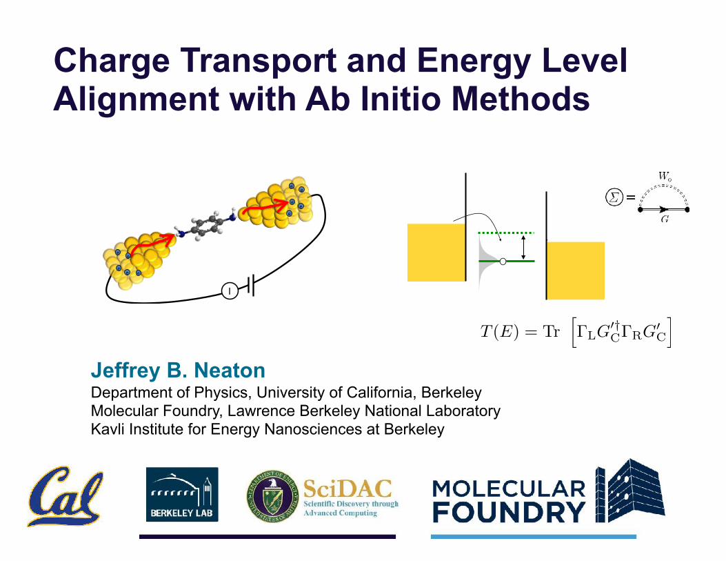
Jeffrey B. Neaton Department of Physics, University of California, Berkeley Molecular Foundry, Lawrence Berkeley National Laboratory Kavli Institute for Energy Nanosciences at Berkeley
Charge Transport and Energy Level Alignment with Ab Initio Methods
I
e"e" e"
e"e"
e"
e"
e"
e"e"
T (E) = Trh�LG
�†C�RG
�C
i
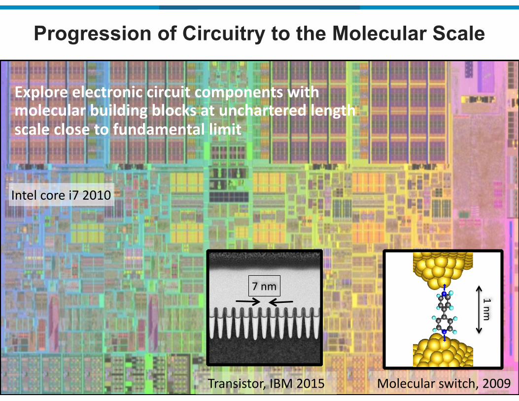
Progression of Circuitry to the Molecular Scale
Intel&core&i7&2010
1&nm
Explore(electronic(circuit(components(with(molecular(building(blocks(at(unchartered(length(scale(close(to(fundamental(limit
Molecular&switch,&2009Transistor,&IBM&2015
7&nm
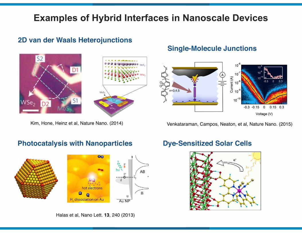
Examples of Hybrid Interfaces in Nanoscale Devices
2D van der Waals Heterojunctions
Kim, Hone, Heinz et al, Nature Nano. (2014)
Photocatalysis with Nanoparticles
Halas et al, Nano Lett. 13, 240 (2013)
Single-Molecule Junctions
Venkataraman, Campos, Neaton, et al, Nature Nano. (2015)
Dye-Sensitized Solar Cells
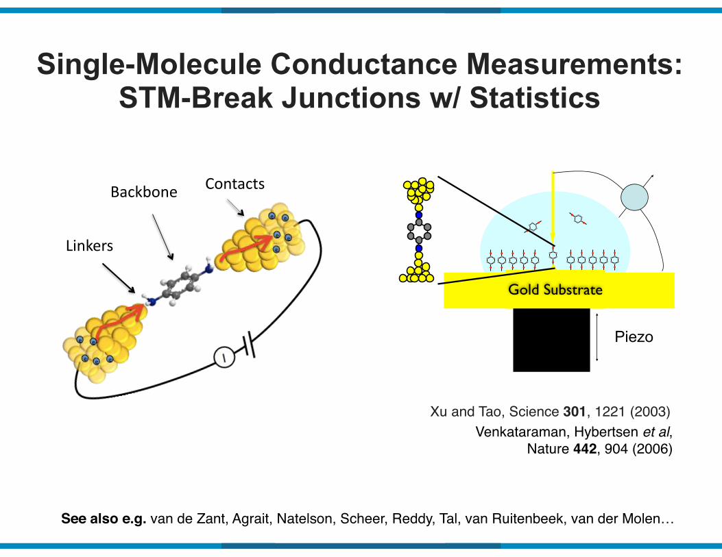
Single-Molecule Conductance Measurements: STM-Break Junctions w/ Statistics
Gold Substrate
Piezo
Venkataraman, Hybertsen et al, Nature 442, 904 (2006)
Xu and Tao, Science 301, 1221 (2003)
See also e.g. van de Zant, Agrait, Natelson, Scheer, Reddy, Tal, van Ruitenbeek, van der Molen…
Linkers
Backbone Contacts

Single-Molecule Conductance Measurements: STM-Break Junctions w/ Statistics
Venkataraman, Hybertsen et al, Nature 442, 904 (2006)
Conductance (G0)C
ou
nts
0.001 0.01 0.1 1
Conductance (G 0)
210
Au NH2NH2
G=0.0064 G0 ± 40%
G0=2e2/h
Au@benzene@diamine@Au
I = GV
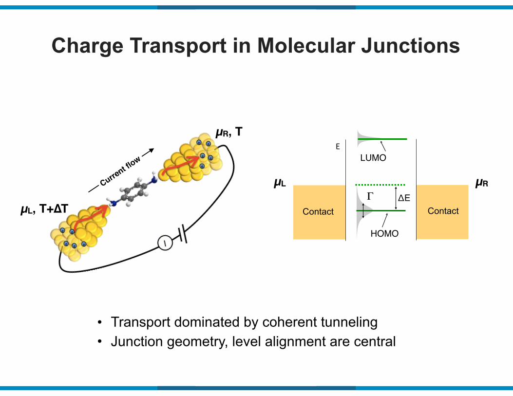
Charge Transport in Molecular Junctions
• Transport dominated by coherent tunneling • Junction geometry, level alignment are central
Contact Contact
E
HOMO
ΔE
LUMO
ΓµL µR
µL, T+∆T
µR, T
Current flow
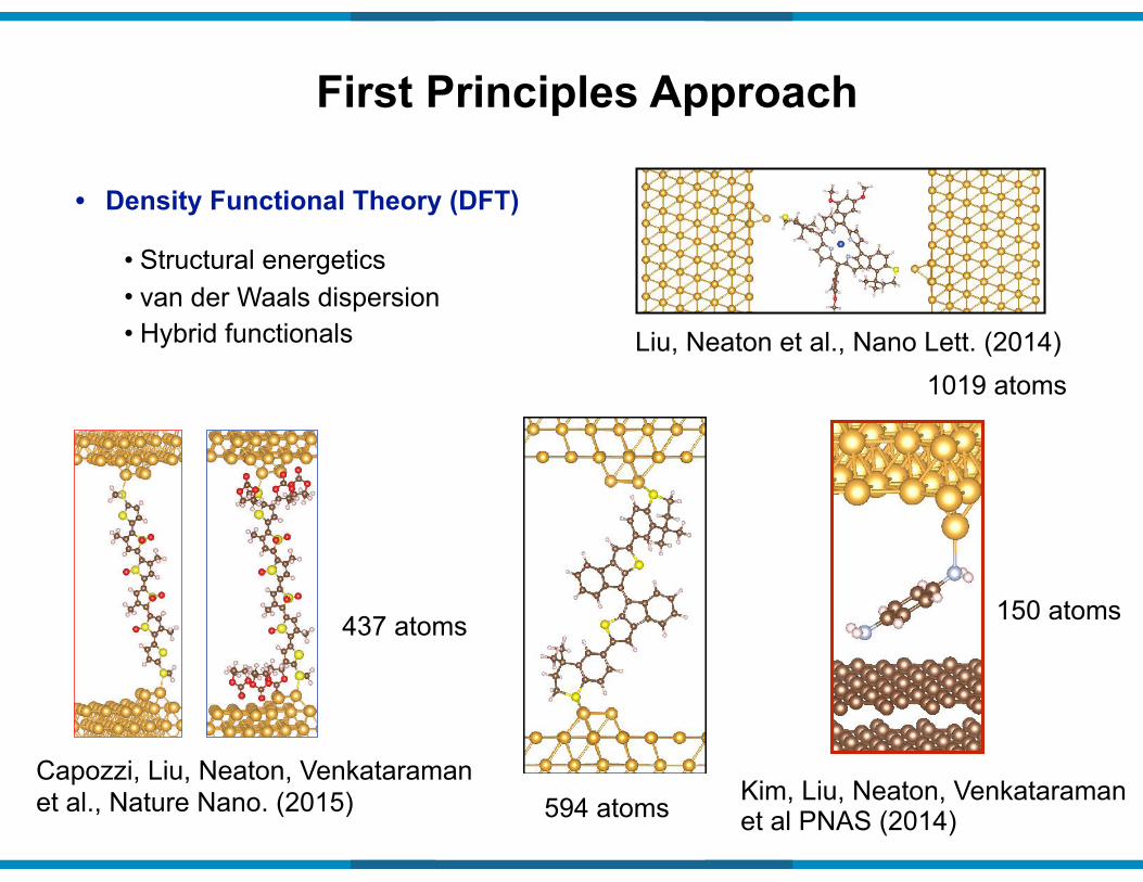
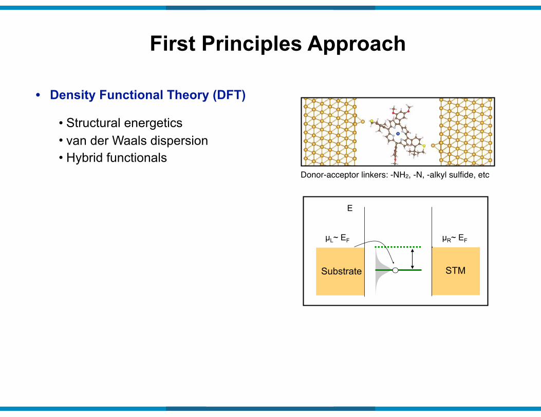
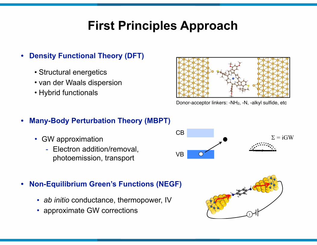
• Structural energetics • van der Waals dispersion • Hybrid functionals
• Density Functional Theory (DFT)
First Principles Approach
1019 atomsLiu, Neaton et al., Nano Lett. (2014)
similar Γ, and that they show a relative shift in ε of ∼0.3 eV. Tomodel a dipole layer on one electrode we added a layer of HF mol-ecules within the unit cell oriented with the dipole pointing towardsor away from the electrode, and computed transmission through theTDO4 junction. Results from these calculations are shown inSupplementary Fig. 12. The presence of a dipole oriented with thenegative charge close to the electrode shifts the resonance positioncloser to EF. We stress here that these are zero-bias calculationsand, as such, cannot be used to quantitatively address the shift inthe resonance position due to an applied bias as this depends onthe double layer density. A first-principles determination of αwould require computing the impact of the double layer aroundthe tip on the resonance position and is beyond the scope ofthis work.
Although we do not have an atomistic model for the observed rec-tification effects, the results from the a.c. measurements and theDFT + Σ calculations support our postulated mechanism. To sum-marize, two factors are needed to observe rectification: (1) electrodesof different areas and (2) an ion-containing polar medium in whichthe transport measurements are performed. Due to the presence of
ions in the environment, an electric double layer forms at each elec-trode/solution interface to screen out any applied bias. The disparateareas of the electrodes result in a denser layer of charge at the smallertip electrode. This results in the pinning of the molecular orbitals tothe chemical potential of the substrate, yielding a current dependenceon the polarity of the applied bias.
We have demonstrated an unconventional technique with whichto create single-molecule diodes with unprecedented rectificationratios at low operating voltages using symmetric molecules. Thisappealing and simple method enables the creation of single-molecule junctions by self-assembly, without the tedious chemicalmodifications that have commonly been used to control moleculedirectionality in a junction7. Given the observed mechanism of rec-tification, we envisage that this method can be easily implementedin other junctions beyond the STM-BJ test bed. For example, theuse of other electrode materials including carbon nanotubes28 orgraphene29 should yield rectifying behaviour. By exploiting thistunable asymmetry in the electrostatic environment, this newapproach offers a wealth of possibilities for translation intodevice fabrication.
Coun
ts
Coun
ts
150a b
c d
100
50
0 00.4 1.00.6
εLUMO (eV)0.8
100
200
300
5 10Γ (meV)
15
α
Γ (m
eV)
0.04
5
6
7
0.5
TCBPC
TCBPC
20
−1.010−5
10−4
10−3
10−2
10−1
100
1.0−0.5 0.50.0Energy − EF (eV)
Tran
smiss
ion
No solventPC
Figure 5 | Experimental and computational determination of energy level alignment. a,b, Experimental determination of orbital coupling strength (a) andenergy level alignment (b) for TDO4 in TCB and PC, determined using a.c. techniques. Inset in a: Orbital coupling as a function of bias asymmetryparameter α. The average value of the coupling for TCB junctions (red asterisk) is only achieved for α = 0.5, which corresponds to a resonance that ispinned to the substrate chemical potential. The dashed line is shown to guide the eye to make the comparison more apparent. c, Junction structures usedto compute transmission functions. d, DFT + Σ calculated transmission functions for TDO4 in a junction with no solvent molecules (red) and with PC onboth electrodes (blue). Dashed lines indicate Lorentzian fits to these transmission functions. These fits yield identical coupling strengths for the conductingorbital (Γ = 13 meV) for both junctions, and show a decrease in orbital position relative to EF when adding PC around the junction (ε = 440 meV, blue;ε = 760 meV, red).
LETTERS NATURE NANOTECHNOLOGY DOI: 10.1038/NNANO.2015.97
NATURE NANOTECHNOLOGY | VOL 10 | JUNE 2015 | www.nature.com/naturenanotechnology526
© 2015 Macmillan Publishers Limited. All rights reserved
Capozzi, Liu, Neaton, Venkataraman et al., Nature Nano. (2015)
437 atoms
594 atoms Kim, Liu, Neaton, Venkataraman et al PNAS (2014)
150 atoms
• Structural energetics • van der Waals dispersion • Hybrid functionals
• Density Functional Theory (DFT)
First Principles Approach
µL~ EF
Substrate
µR~ EF
STM
E
Donor-acceptor linkers: -NH2, -N, -alkyl sulfide, etc
• Structural energetics • van der Waals dispersion • Hybrid functionals
• Density Functional Theory (DFT)
First Principles Approach
• GW approximation - Electron addition/removal,
photoemission, transport
First-Principles Study of Material PropertiesFirst-Principles Study of Material Properties
+
! = iGW
(electrons in ground state)
Fermi sea
Fermi sea
(excitonic)
(behavior of excited particles)CB
VB
• Many-Body Perturbation Theory (MBPT)
• ab initio conductance, thermopower, IV • approximate GW corrections
I
e"e" e"
e"e"
e"
e"
e"
e"e"
• Non-Equilibrium Green’s Functions (NEGF)
Donor-acceptor linkers: -NH2, -N, -alkyl sulfide, etc
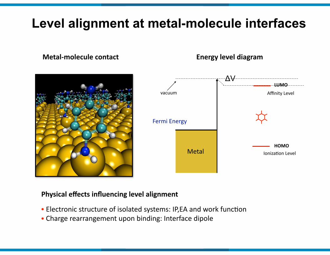
Level alignment at metal-molecule interfaces
Metal9molecule(contact Energy(level(diagram
Fermi&Energy&
Metal
vacuum Affinity&Level
IonizaIon&LevelHOMO
LUMO
Physical(effects(influencing(level(alignment(
•&Electronic&structure&of&isolated&systems:&IP,EA&and&work&funcIon&&•&Charge&rearrangement&upon&binding:&Interface&dipole
ΔV
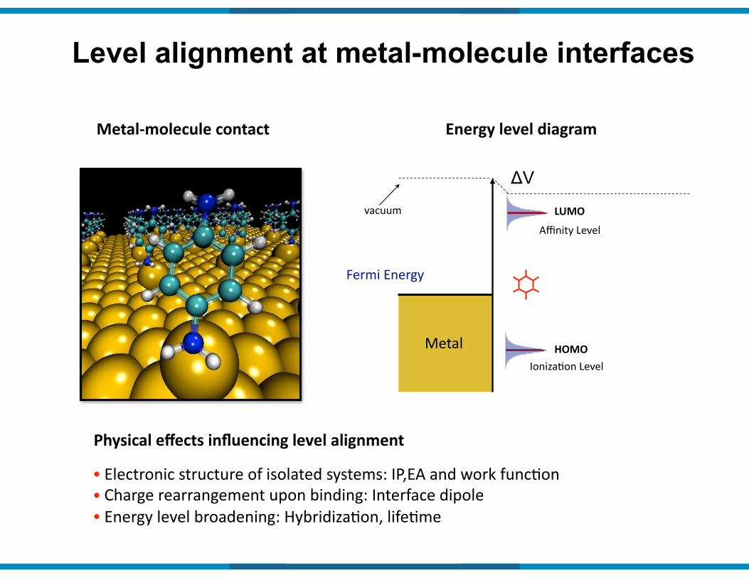
Metal9molecule(contact Energy(level(diagram
Fermi&Energy&
Metal
vacuum
IonizaIon&LevelHOMO
Affinity&Level
LUMO
ΔV
Physical(effects(influencing(level(alignment(
•&Electronic&structure&of&isolated&systems:&IP,EA&and&work&funcIon&&•&Charge&rearrangement&upon&binding:&Interface&dipole& •&Energy&level&broadening:&HybridizaIon,&lifeIme
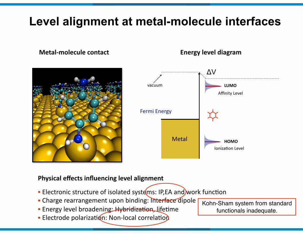
Level alignment at metal-molecule interfaces
Metal9molecule(contact Energy(level(diagram
Fermi&Energy&
Metal
vacuum
ΔV
Affinity&Level
LUMO
IonizaIon&LevelHOMO
Physical(effects(influencing(level(alignment(
•&Electronic&structure&of&isolated&systems:&IP,EA&and&work&funcIon&•&Charge&rearrangement&upon&binding:&Interface&dipole&•&Energy&level&broadening:&HybridizaIon,&lifeIme&&•&Electrode&polarizaIon:&Non@local&correlaIon
Kohn-Sham system from standard functionals inadequate.
Level alignment at metal-molecule interfaces

Metal9molecule(contact Energy(level(diagram
Fermi&Energy&
Metal
vacuum
ΔV
Affinity&Level
LUMO
IonizaIon&LevelHOMO
Physical(effects(influencing(level(alignment(
•&Electronic&structure&of&isolated&systems:&IP,EA&and&work&funcIon&•&Charge&rearrangement&upon&binding:&Interface&dipole&•&Energy&level&broadening:&HybridizaIon,&lifeIme&&•&Electrode&polarizaIon:&Non@local&correlaIon
Level alignment at metal-molecule interfaces
Kohn-Sham system from standard functionals inadequate.
Generalized Kohn-Sham system from hybrid functionals is quite promising (see later in the talk)
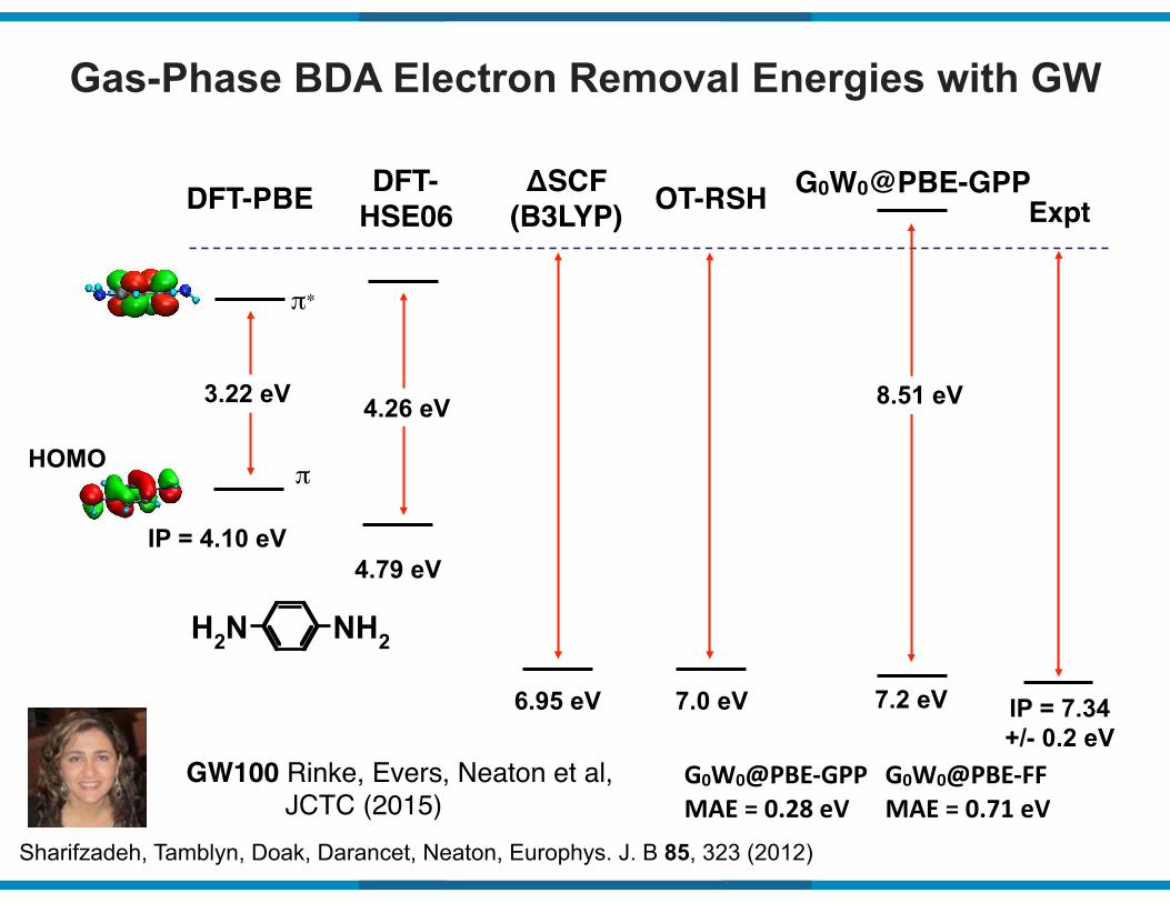
Gas-Phase BDA Electron Removal Energies with GW
IP = 4.10 eV
3.22 eV
π
DFT-PBE
π∗
Expt
IP = 7.34 +/- 0.2 eV
8.51 eV
G0W0@PBE-GPP
7.2 eV
NH2NH2
Sharifzadeh, Tamblyn, Doak, Darancet, Neaton, Europhys. J. B 85, 323 (2012)
HOMO
DFT-HSE06
4.26 eV
4.79 eV
ΔSCF(B3LYP)
6.95 eV
OT-RSH
7.0 eV
G0W0@PBE9GPP(MAE(=(0.28(eV
G0W0@PBE9FF(MAE(=(0.71(eV
GW100 Rinke, Evers, Neaton et al, JCTC (2015)

Neaton, Hybertsen, Louie, Phys. Rev. Lett. 97, 216405 (2006)
Molecular Levels Strongly Renormalized in Junction
Benzene @ graphite: Frontier electronic pi orbitals
EF
Benzene @ graphite: Computed Level Diagram
Graphite
Isolated moleculeMetal-molecule interface
• Nonlocal electronic correlations, not present in DFT, between the molecule and substrate reduce gap
• Effect approximately captured by classical electrostatics
10.5 eV
GW
π
π∗
7.3 eV
GW
5.1 eV
DFT
5.1 eV
DFT
Corroborated by Thygesen, Rubio, Rinke, Sanvito
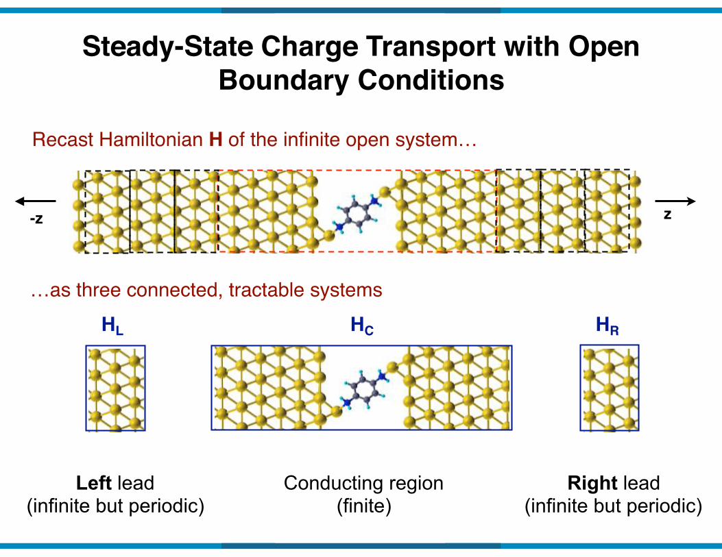
Steady-State Charge Transport with Open Boundary Conditions
Recast Hamiltonian H of the infinite open system…
…as three connected, tractable systems
Right lead (infinite but periodic)
Left lead (infinite but periodic)
Conducting region (finite)
HL HC HR
z-z
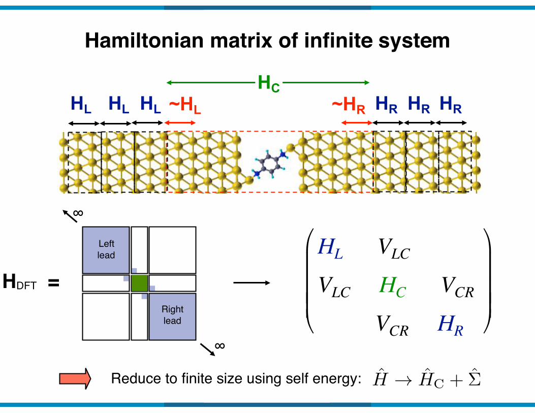
Hamiltonian matrix of infinite system
∞
∞
HDFT =
€
HL VLCVLC∗ HC VCR
VCR∗ HR
#
$
% % %
&
'
( ( (
HL VLC
VLC HC VCR
VCR HR
HR HR HRHL HL HL
Reduce to finite size using self energy:
HC~HL ~HR
Left lead
Right lead
H ! HC + �
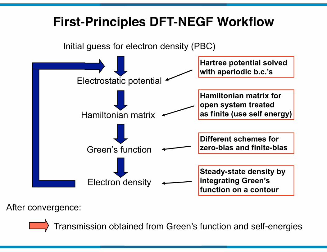
Initial guess for electron density (PBC)
Electrostatic potential
Hamiltonian matrix
Green’s function
Electron density
First-Principles DFT-NEGF Workflow
Hartree potential solved with aperiodic b.c.’s
Different schemes for zero-bias and finite-bias
Steady-state density by integrating Green’s function on a contour
Hamiltonian matrix for open system treated as finite (use self energy)
Transmission obtained from Green’s function and self-energies
After convergence:
Green’s function and the densityzero-bias
D = � 1
⇡Im
Z 1
�1d✏G(✏+ i�)nF (✏� µ)
�.
Neq energy grid
finite-bias
2*Neq+Nneq energy grid
extra step: triple product
G(E) = [ES�HC �⌃L(E)�⌃R(E)]�1
total time ~ Neq total time ~ 2Neq + Nneq + 2(triple product)
30 ~ 40 SCF cycles,each cycle 10 ~ 15 mins
100 ~ 150 SCF cycles,each cycle 30mins ~ 1hour
Brandbyge et al, Phys. Rev B 65, 165401 (2002)
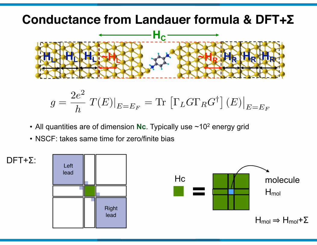
Conductance from Landauer formula & DFT+Σ
g =2e2
hT (E)|E=EF
= Tr⇥�LG�RG
†⇤ (E)��E=EF
HC
• All quantities are of dimension Nc. Typically use ~102 energy grid• NSCF: takes same time for zero/finite bias
HR HR HRHL HL HL ~HL ~HR
DFT+Σ:Left lead
Right lead
=Hc moleculeHmol
Hmol ⇒ Hmol+Σ

DFT+Σ: Model GW Self-Energy Correction
Hc ! Hc +X
mol
⌃mol
| mol
ih mol
|• ‘One-shot’ correction
Figure 1: Diagram of model for self-energy correction to molecular levels in a weakly coupled
junction within the DFT+Σ method for transport computation. The correction has two parts: a
gas-phase term, equal to the difference between Kohn-Sham eigenvalues and quasiparticle levels in
the gas phase, which in general opens the HOMO-LUMO gap; and an electrode polarization term,
due to metallic screening by the leads of added charge on the molecule, which reduces the gap.
be neglected; organic molecules with ϵ∞ ∼ 2 (in liquid form) easily meet this. (3) The
transmission spectra at the DFT level (Fig. 5) as a proxy for the DFT density of states
show that the peaks only slightly overlap the Fermi level, clearly seen quantitatively from
the fact that the transmission at the Fermi level is much less than unity. Thus our needed
criteria are met for this set of molecules.
For corrections to the HOMO, Σ0 is obtained by taking the difference between the gas-
phase ionization potential (IP) and the DFT KS HOMO eigenvalue, and analogously for
the LUMO with the electron affinity (EA). Our calculations use an isolated molecule in the
geometry from the relaxed junction. We compute the IP and EA using the ∆SCF method,95
employing GAUSSIAN03 with the B3LYP exchange-correlation functional and 6-311g++dp
basis set.96 This procedure gives IP values within 0.1 eV of experiment97 for our set of
molecules.
The image-charge term ∆Σ is computed using an electrostatic model that assumes the two
15
Gas-phase correction from OT-RSH or GW calculation
for gas-phase molecule
• Two terms, no adjustable parameters
Electrode polarization from an image charge calculation of electrode
polarization energy
Quek et al, Nano Lett. 7, 3477 (2007)Quek et al, Nano Lett. 9, 3949 (2009)Darancet et al, Nano Lett. 12, 6250 (2012)Liu et al, Nano Lett. 14, 5365 (2014)Egger et al, Nano Lett. 15, 2448 (2015)
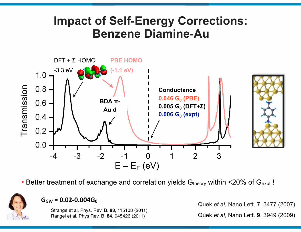
Impact of Self-Energy Corrections: Benzene Diamine-AuTr
ansm
issi
on
E – EF (eV)
Quek et al, Nano Lett. 7, 3477 (2007)
• Better treatment of exchange and correlation yields Gtheory within <20% of Gexpt !
Quek et al, Nano Lett. 9, 3949 (2009)
0.005 G0 (DFT+Σ)0.006 G0 (expt)
0.046 G0 (PBE)Conductance
BDA π- Au d
DFT + Σ HOMO
-3.3 eV
PBE HOMO (-1.1 eV)
GGW(=(0.0290.004G0
Strange et al, Phys. Rev. B. 83, 115108 (2011)Rangel et al, Phys Rev. B. 84, 045426 (2011)
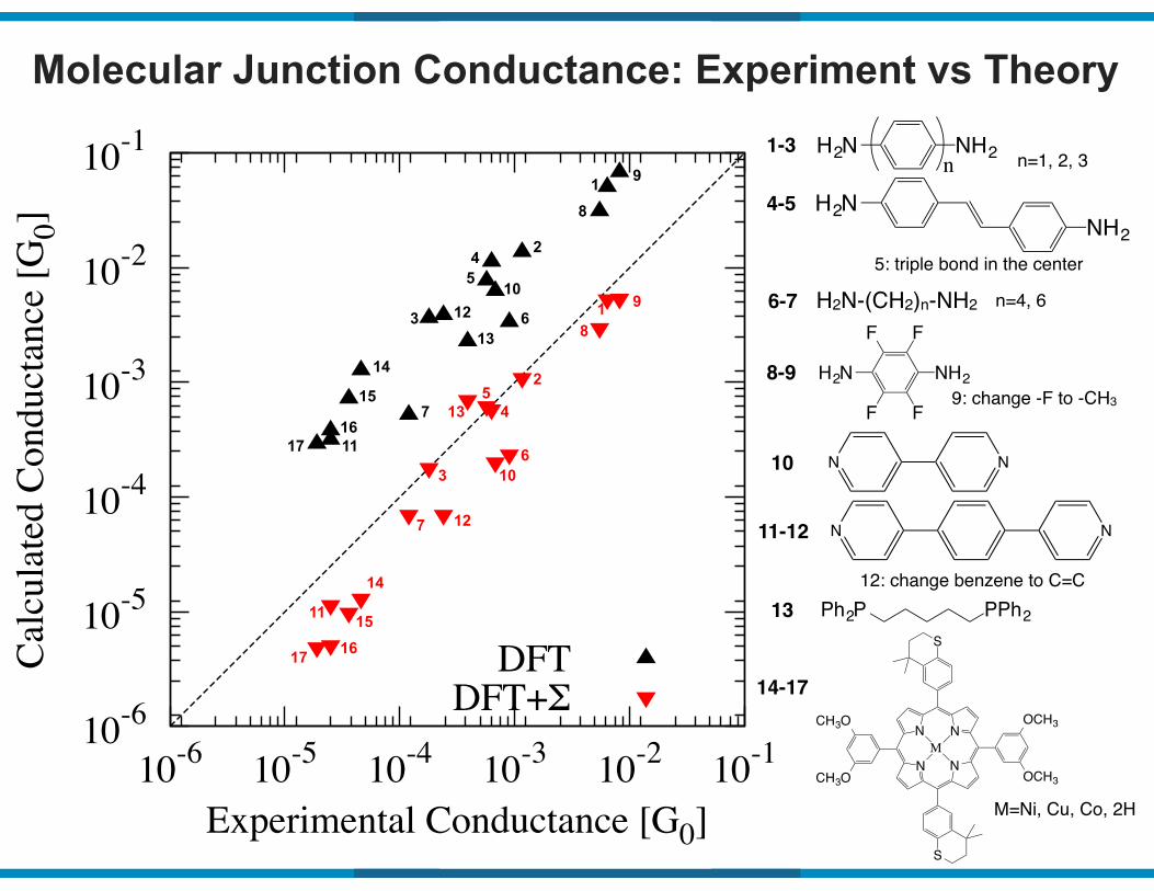
Molecular Junction Conductance: Experiment vs Theory
10-6
10-5
10-4
10-3
10-2
10-1
10-6 10-5 10-4 10-3 10-2 10-1
Cal
cula
ted
Con
duct
ance
[G0]
Experimental Conductance [G0]
DFTDFT+Σ
1
2
3
45
6
7
8
9
10
11
1213
14
15
1617
1
2
3
45
6
7
8
9
10
11
12
13
14
151617
Ph2P PPh2
N
N N
N
S
S
M
CH3O
CH3O
OCH3
OCH3
H2N NH2
F F
F F
H2N NH2
H3C CH3
H3C CH3
M=Ni, Cu, Co, 2H
1-3
6-7
8-9
13
14-17
H2N NH2n
H2N-(CH2)n-NH2 n=4, 6
n=1, 2, 3
H2NNH2
4-5
5: triple bond in the center
9: change -F to -CH3
N N
N N
10
11-12
12: change benzene to C=C

Validity of DFT+Σ, an approx. GW approach
• “Weakly coupled” junctions: ➡ Molecular states unchanged in junction ➡ Frontier orbitals are far from EF
➡ Substrate polarization treated with image charge physics
• Neglect ➡ Charge transfer between molecule & lead ➡ Changes in molecular polarizability ➡ Lead eigenstate self-energy corrections
Lead LeadΣ
EF
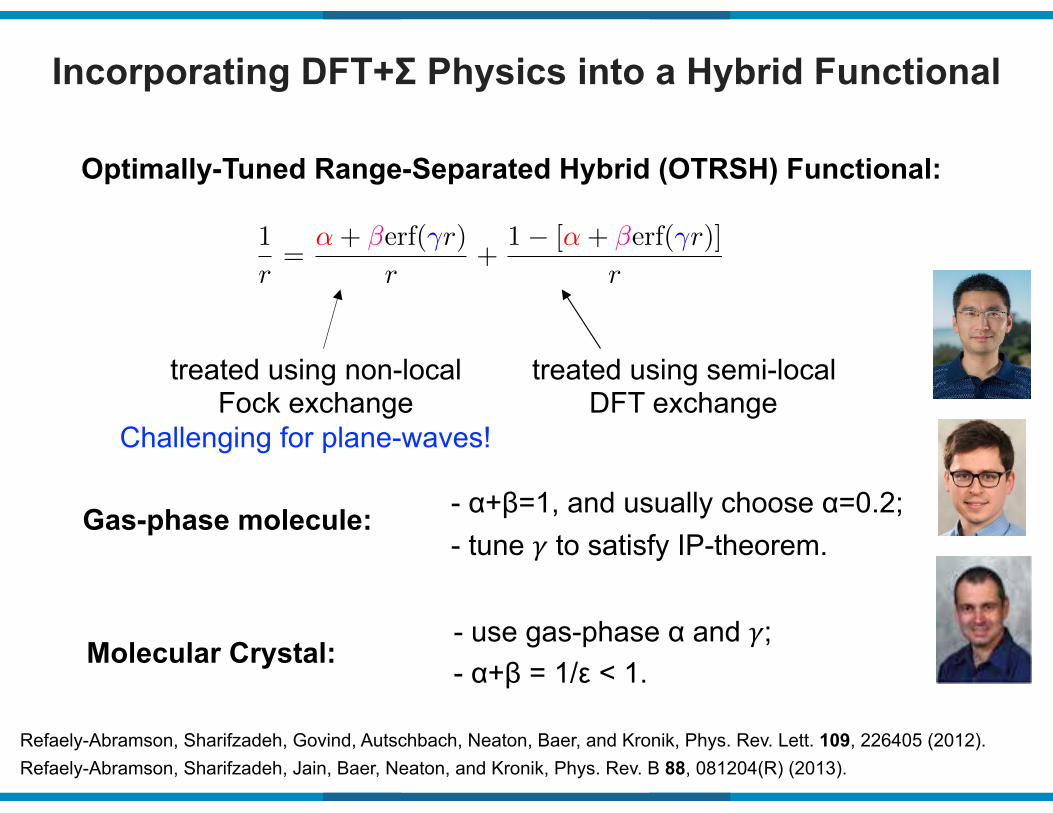
Incorporating DFT+Σ Physics into a Hybrid Functional
Optimally-Tuned Range-Separated Hybrid (OTRSH) Functional:
1
r=
↵+ �erf(�r)
r+
1� [↵+ �erf(�r)]
r
treated using non-local Fock exchange
treated using semi-local DFT exchange
Refaely-Abramson, Sharifzadeh, Govind, Autschbach, Neaton, Baer, and Kronik, Phys. Rev. Lett. 109, 226405 (2012).Refaely-Abramson, Sharifzadeh, Jain, Baer, Neaton, and Kronik, Phys. Rev. B 88, 081204(R) (2013).
Gas-phase molecule: - α+β=1, and usually choose α=0.2;- tune ! to satisfy IP-theorem.
Molecular Crystal:- use gas-phase α and !;- α+β = 1/ε < 1.
Challenging for plane-waves!

Optimally-Tuned RSH Functional for Interfaces
❶ Use gas-phase molecular α and !;
❷ For the metal slab, find the image plane z0:
Egger, Liu, Neaton, and Kronik, Nano Lett. 15, 2448 (2015).
❸ Compute image-charge interaction P =1
4|z � z0|
For a specific molecule-metal interface:
Liu, Egger, Refaely-Abramson, Kronik, and Neaton, in prep. (2016).
❹ Tune β such that:
"H(�)� "H(�0) = P
-8.2
-8
-7.8
-7.6
-7.4
-7.2
-7
-6.8
-6.6
-6.4
-0.2 0 0.2 0.4 0.6 0.8
HO
MO
(e
V)
β
PTCDA as an example
Currently only implemented for norm-conserving pseudopotential.
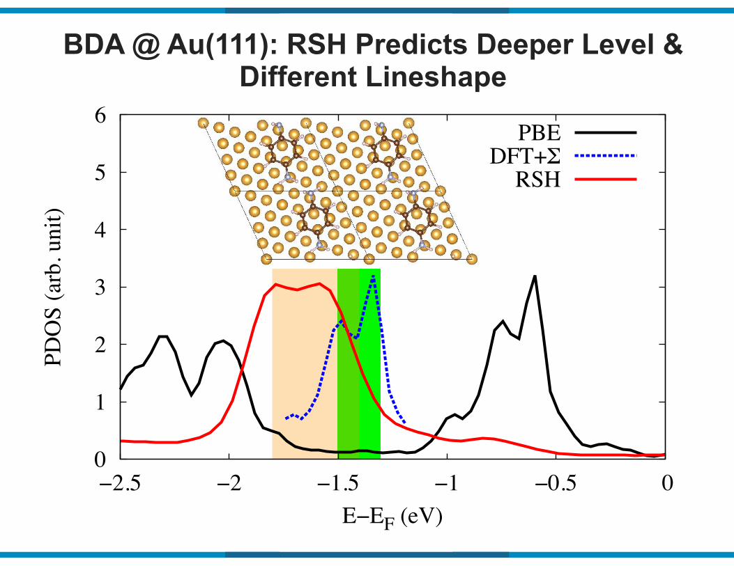
BDA @ Au(111): RSH Predicts Deeper Level & Different Lineshape
0
1
2
3
4
5
6
−2.5 −2 −1.5 −1 −0.5 0
PDO
S (a
rb. u
nit)
E−EF (eV)
PBEDFT+Σ
RSH
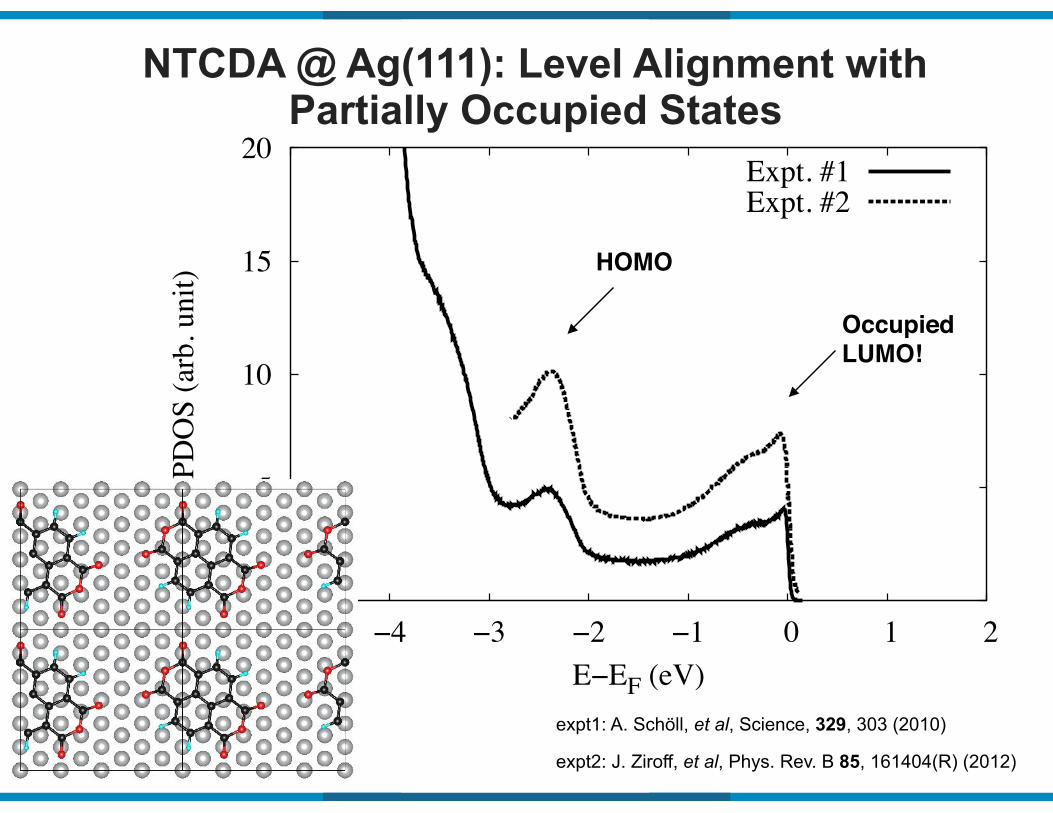
NTCDA @ Ag(111): Level Alignment with Partially Occupied States
expt1: A. Schöll, et al, Science, 329, 303 (2010)
expt2: J. Ziroff, et al, Phys. Rev. B 85, 161404(R) (2012)
0
5
10
15
20
−5 −4 −3 −2 −1 0 1 2
PDO
S (a
rb. u
nit)
E−EF (eV)
Expt. #1Expt. #2
HOMO
Occupied LUMO!
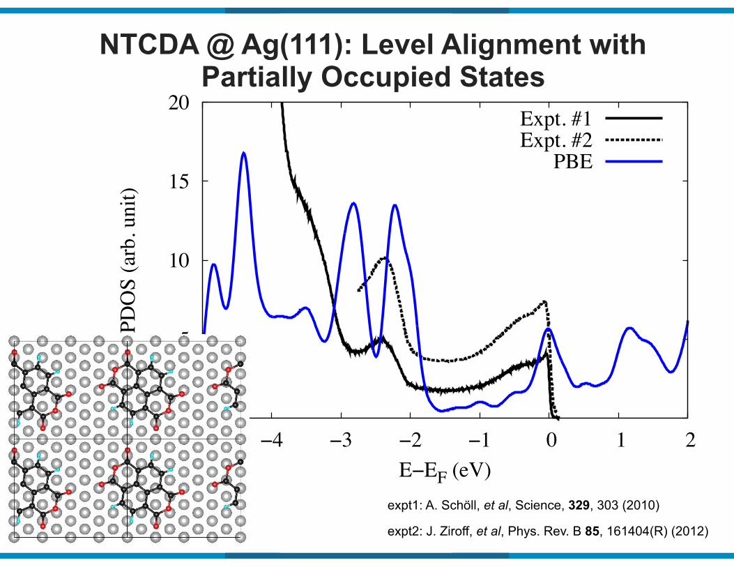
NTCDA @ Ag(111): Level Alignment with Partially Occupied States
expt1: A. Schöll, et al, Science, 329, 303 (2010)
expt2: J. Ziroff, et al, Phys. Rev. B 85, 161404(R) (2012)
0
5
10
15
20
−5 −4 −3 −2 −1 0 1 2
PDO
S (a
rb. u
nit)
E−EF (eV)
Expt. #1Expt. #2
PBE

expt1: A. Schöll, et al, Science, 329, 303 (2010)
expt2: J. Ziroff, et al, Phys. Rev. B 85, 161404(R) (2012)
NTCDA @ Ag(111): Level Alignment with Partially Occupied States
0
5
10
15
20
−5 −4 −3 −2 −1 0 1 2
PDO
S (a
rb. u
nit)
E−EF (eV)
Expt. #1Expt. #2
PBERSH (β=−0.0833)

OT-RSH Applied to Molecular Junctions
hexane
Refaely-Abramson, Liu, Neaton et al., in prep.
0
2
4
6
8
10
12
14
16
-3 -2 -1 0 1 2 3
DO
S (
arb
. unit
)
E-E_F (eV)
PBERSH
PDOS only, no transport yet.
Transport with peptides - need to understand how -COOH binds to Au surface.
-COO bindingno obvious gas-phase referenceDFT+Σ does not directly apply
A different reference: mol + 3Au
eigenchannel ~HOMO-2
Study the difference between peptides and alkanes on decay constant β: g ~ exp(-βL).

Collaborators Latha Venkataraman, Columbia Mark Hybertsen, BNL Steven Louie, UC-Berkeley Luis Campos, Columbia Leeor Kronik, Weizmann Institute
Group members (this work) Zhenfei Liu Michele Kotiuga (Rutgers) Sahar Sharifzadeh (Boston Univ.) Pierre Darancet (Argonne Nat’l Lab) Isaac Tamblyn (UOIT, Ottawa) Su Ying Quek (NUS, Singapore)
Acknowledgements


![Welcome... []barlow/preprints/gw100.pdf · 2005. 3. 4. · Welcome](https://img.pdfslide.net/doc/110x75/60c62efa12a4697e3b3f34b3/welcome-barlowpreprintsgw100pdf-2005-3-4-welcome.jpg)