Embed Size (px)
Citation preview


foreword On behalf of the Organising and the International Scientific Committees we take great pleasure in welcoming you to Dresden (Germany) for the 2nd edition of the European Conference on Chemistry of Two-Dimensional Materials (chem2Dmat2019).
During the last years, the chemistry of graphene has played an ever-increasing role in the large-scale production, chemical functionalization and processing as well as in numerous applications of such material, and it has been expanded to various new 2D inorganic and organic materials. This conference aims at providing a forum to the rapidly growing community of scientists mastering the chemical approaches to 2D materials in order to fabricate systems and devices exhibiting tunable performance. The chemical approach offers absolute control over the structure of 2D materials at the atomic- or molecular-level and will thus serve as enabling strategy to develop unprecedented multifunctional systems, of different complexity, featuring exceptional physical or chemical properties with full control over the correlation between structure and function.
The 2nd edition of chem2Dmat will cover all areas related to 2D materials' chemistry spanning their synthesis as well as their functionalization, using covalent and non-covalent approaches, for composites, foams and coatings, membranes, (bio-)sensing, (electro- and photo-)catalysis, energy conversion, harvesting & storage, electronics, nanomedicine and biomaterials.
chem2Dmat2019 Highlights:
• Expected attendance: 200 participants
• 34 Keynotes & Invited Speakers
• 60 posters
• Nearly 65 oral contributions
• 1/2-day Industrial Forum in parallel to get an updated understanding of Graphene based technologies
• 5 awards to PhD students
chem2Dmat2019 is now an established event, attracting global participant’s intent on sharing, exchanging and exploring new avenues of graphene-related scientific and commercial developments.
We are also indebted to the following Scientific Institutions, Companies and Government Agencies for their help and/or financial support: Technische Universität Dresden, Deutsche Forschungsgemeinschaft (DFG, German Research Foundation), Advanced Materials/Wiley, Journal of Carbon Research/MDPI, Materials Horizons-Nanoscale Horizons/RSC and Nanoscale-Nanoscale Advances/RSC.
We also would like to thank all the exhibitors, speakers and participants that join us this year. In addition, thanks must be given to the staff of all the organizing institutions whose hard work has helped planning this conference.
We truly hope that chem2Dmat2019 serves as an international platform for communication between science and business.
Hope to see you again in the next edition of chem2Dmat to be held in 2021.
main organisers
5
committees
Organising Committee Antonio Correia (Phantoms Foundation, Spain) Xinliang Feng (TU Dresden / cfaed, Germany) Paolo Samorí (Université de Strasbrourg / CNRS, France)
local organizing committee Xinliang Feng (TU Dresden / cfaed, Germany) Thomas Heine (TU Dresden Germany) Michael Ruck (TU-Dresden, Germany) Gianaurelio Cuniberti (TU-Dresden, Germany)
international scientific committee Alberto Bianco (CNRS - Institut de Biologie Moléculaire et Cellulaire, France) Francesco Bonaccorso (IIT-Graphene Labs / BeDimensional SpA, Italy) Cinzia Casiraghi (University of Manchester, United Kingdom) Jonathan Coleman (Trinity College Dublin, Ireland) Xinliang Feng (Dresden University of Technology, Germany) Andrea Ferrari (University of Cambridge, United Kingdom) Andreas Hirsch (University of Erlangen-Nürnberg, Germany) Ian Kinloch (University of Manchester, United Kingdom) Klaus Müllen (MPI Mainz, Germany) Konstantin Novoselov (University of Manchester, United Kingdom) Vincenzo Palermo (Chalmers University of Technology, Sweden) Anne Pichon (Nature Chemistry, UK) Maurizio Prato (University of Trieste, Italy) Stephan Roche (ICREA – ICN2, Spain) Ester Vázquez (University of Castilla-la Mancha, Spain)
Secretaries Natalia León Martínez (Phantoms Foundation, Spain) Concepción Narros Hernández (Phantoms Foundation, Spain) José Luis Roldán Hernández (Phantoms Foundation, Spain)
6
awards
sponsors
7
exhibitors
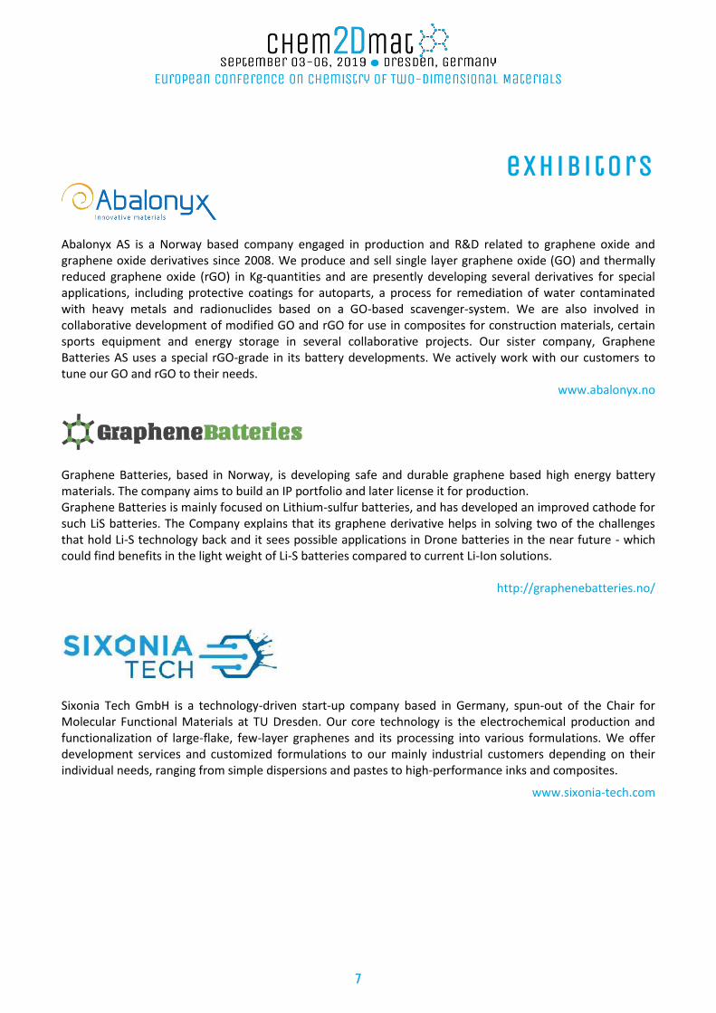
Abalonyx AS is a Norway based company engaged in production and R&D related to graphene oxide and graphene oxide derivatives since 2008. We produce and sell single layer graphene oxide (GO) and thermally reduced graphene oxide (rGO) in Kg-quantities and are presently developing several derivatives for special applications, including protective coatings for autoparts, a process for remediation of water contaminated with heavy metals and radionuclides based on a GO-based scavenger-system. We are also involved in collaborative development of modified GO and rGO for use in composites for construction materials, certain sports equipment and energy storage in several collaborative projects. Our sister company, Graphene Batteries AS uses a special rGO-grade in its battery developments. We actively work with our customers to tune our GO and rGO to their needs.
www.abalonyx.no
Graphene Batteries, based in Norway, is developing safe and durable graphene based high energy battery materials. The company aims to build an IP portfolio and later license it for production. Graphene Batteries is mainly focused on Lithium-sulfur batteries, and has developed an improved cathode for such LiS batteries. The Company explains that its graphene derivative helps in solving two of the challenges that hold Li-S technology back and it sees possible applications in Drone batteries in the near future - which could find benefits in the light weight of Li-S batteries compared to current Li-Ion solutions.
http://graphenebatteries.no/
Sixonia Tech GmbH is a technology-driven start-up company based in Germany, spun-out of the Chair for Molecular Functional Materials at TU Dresden. Our core technology is the electrochemical production and functionalization of large-flake, few-layer graphenes and its processing into various formulations. We offer development services and customized formulations to our mainly industrial customers depending on their individual needs, ranging from simple dispersions and pastes to high-performance inks and composites.
www.sixonia-tech.com
8
Speakers Index alphabetical order
page Mohsen Aadeli (Freie Universitaet, Germany) Study on the Mechanism of Graphene/Pathogen interactions
Oral 52 Jorge Eduardo Adatti Estevez (Infineon, Germany) High-yield production and characterization of graphene-based chemiresistors for environmental sensing
InvitedIF
47 Ishfaq Ahmad (UNIST, South Korea) Robust fused aromatic pyrazine-based two-dimensional network for stably cocooning iron nanoparticles as an oxygen reduction electrocatalyst
Poster
115 Adriana Alieva (University of Manchester, UK) Effect of Graphene on the Crystallisation of Glycine
Oral 53 Stevan Andric (Institute of Chemistry, Technology, and Metallurgy, Serbia) Humidity sensing with Langmuir-Blodgett assembled graphene films from liquid phase
Poster
116 Florian M. Arnold (TU Dresden, Germany) The Influence of the Twist Angle on the Properties of Transition Metal Dichalcogenide Bilayers
Poster
117 Sehrish Aslam (Harbin Institute of Technology, China) Mixed-dimensional Heterostructure of Graphene Foam for Tunable Ecofriendly Hydrogen Evolution Reaction
Poster
118 Mhamed Assebban (ICMol - UV, Spain / ZMP - FAU Erlangen-Nürnberg, Germany) Towards optimized preparation of few-layer antimonene and unveiling its oxidation tendency
Oral
54 Kannan Balasubramanian (Humboldt Universität zu Berlin, Germany) The unique interplay between interfacial chemistry and electronic structure in graphene
Oral
55 Shashank Balasubramanyam (TU/e, The Netherlands) Edge-site nano-engineering of WS2 by low temperature plasma-enhanced atomic layer deposition for electrocatalytic hydrogen evolution
Poster
119 José J. Baldoví (Max Planck Institute for the Structure and Dynamics of Matter, Germany) Ab initio study of ultrasensitive H2S gas sensors based WS2 hybrid materials
Poster
120 Tanmay Banerjee (Max Planck Institute for Solid State Research, Germany) 2D covalent organic frameworks with built-in functional groups by sub-stoichiometric topological design
Oral
56 Cian Bartlam (University of Manchester, UK) Nanoscale Infrared Characterisation of Functional Groups on Two-dimensional Materials
Oral
57 Thomas Bein (Ludwig-Maximilians-Universität München, Germany) Optoelectronic Processes in Covalent Organic Frameworks
Invited 24 Alberto Bianco (IBMC-CNRS-Université de Strasbourg, France) Multifunctional biodegradable graphene-based materials for cancer therapy
Invited 25 Luca Bignardi (University of Trieste, Italy) Highly-ordered single-layer MoS2 on the anisotropic Ag(110)
Oral 58 Nerea Bilbao (KU Leuven, Belgium) On-Surface Synthesis of Covalent Organic Frameworks
Oral 59
9
page Matias Blanco (University of Padova, Italy) Enhanced carbocatalytic alcohol oxidation by Graphene Acid: Mechanistic insights for the control of the selectivity
Oral
60 Ivan Bobrinetskiy (Biosense Institute, Serbia) In-plane junctions in graphene field-effect transistors generated by photochemical mask-less patterning
Oral
61 Francesco Bonaccorso (IIT-Graphene Labs / BeDimensional, Italy) Liquid phase production of 2D crystals for energy applications
Invited 26 Anton Brown (KU Leuven, Belgium) Self-Assembled Monolayers as Templates for Linearly Nanopatterned Covalent Chemical Functionalization of Graphite and Graphene Surfaces
Poster
121 Alexandra Burger (Friedrich-Alexander-Universität Erlangen-Nürnberg, Germany) Electrochemical Exfoliation of Black Phosphorus
Poster 122 Stefano Casalini (University of Strasbourg, France) Reduced graphene oxide transistors: towards wearable e-platforms
Oral 62 Cinzia Casiraghi (University of Manchester, UK) Water-based 2D-Inks: from all-inkjet printed devices to biomedical applications
Invited 27 Jiri Cervenka (FZU - Institute of Physics of the CAS, Czech Republic) Chemical and Biomolecule Sensing using Graphene Field Effect Transistors
Oral 63 Hui Chen (Institute of Physics, The Chinese Academy of Sciences, China) Large-scale formation of single-crystal one-third-hydrogenated graphene with anisotropic electronic properties
Oral
64 Long Chen (Tianjin University, China) De Novo Design and Facile Synthesis of 2D Covalent Organic Frameworks: A Two-in-One Strategy
Oral
65 Bing-Ming Cheng (National Synchrotron Radiation Research Center, Taiwan) Fluorescent Nitrogen-vacancy Diamond as VUV Sensor
Oral 66 Dimitrios Chronopoulos (Palacky University / RCPTM, Czech Republic) Alkynylation of Graphene via Sonogashira C-C Cross Coupling Reaction on Fluorographene
Oral
67 Jonathan Coleman (Trinity College Dublin, Ireland) 2D-based composites as battery electrodes
Invited 28 Camilla Coletti (IIT, Italy) Going beyond copper: wafer-scale synthesis of graphene on sapphire
Invited 29 Conor Cullen (Trinity College Dublin, Ireland) Nitrogen Doping of CVD-MoS2 via soft plasma treatment
Poster 123 Lakshya Daukiya (KU Leuven, Belgium) SPM studies on functionalization of 2D transition metal dichalcogenides
Oral 68 Steven De Feyter (KU Leuven, Belgium) Periodic Non-Covalent and Covalent Functionalization of 2D Materials
Invited 30 Joris de la Rie (University of Groningen, The Netherlands) Self-Assembly of Para-Hexaphenyl-Dicarbonitrile on Graphitic substrates: H-bonding and Metal-Organic Coordination
Poster
124 Lucia Gemma Delogu (University of Padua, Italy) Future applications for 2D materials: the immune system scenario
InvitedPW 37 William Dichtel (Northwestern University, USA) Advances in 2D Polymerization
Keynote - Mircea Dinca (Massachusetts Institute of Technology, USA) Electrical Conductivity in 2D Metal-Organic Frameworks
Keynote 17
10
page Christian Dolle ((ICMol) - Universidad de Valencia, Spain) Cleaning graphene using the NanoBroom
Oral 68 Renhao Dong (TU Dresden, Germany) Interfacial Synthesis of 2D Conjugated Polymers: the Rise of Organic 2D Materials
Oral 69 Shixuan Du (Chinese Academy of Sciences, China) Electronic-Structure Engineering of Graphene by Semiconductor Intercalation
Invited 31 Georg Stefan Duesberg (Universität der Bundeswehr München, Germany) Functionalisation Strategies of Monolayer Surfaces
Invited 32 Siegfried Eigler (Freie Universität Berlin, Germany) Oxo-Graphene – Synthesis and Heterostructures
InvitedPW 38 Roman Fasel (EMPA, Switzerland) Nanographenes with intrinsic π-magnetism
Keynote 18 Laura Fernandez Gomez-Recuero (UPV/EHU, Spain) Induced facet formation due to the growth of hexagonal Boron Nitride on curved Ni(111)
Poster
125 Michael Fickert (FAU Erlangen-Nürnberg, Germany) Exfoliation, oxidation and functionalization of antimonene
Poster 126 Pascal Freund (Trevira GmbH, Germany) Conductivity and more?: GRM enables new properties in PET filaments
InvitedIF 48 Emil Fuhry (Humboldt-Universität zu Berlin, Germany) Separation and detection of antioxidants using a graphene-based electrochemical sensor platform
Poster
127 Sai Manoj Gali (Université de Mons - UMONS, Belgium) Electronic structure and charge transport simulations in GRM-organic hybrids: Where Chemistry meets Physics
Invited
33 Claudio Gasparini (CNR - ISOF, Italy) Triboelectric composites obtained by electrospinning of PVdF/GO nanofibers
Poster 128 Sadegh Ghaderzadeh (Helmholtz-Zentrum Dresden-Rossendorf, Germany) MoS2 monolayers under cluster ion irradiation: A molecular dynamics study
Poster 129 Tobias Grosser (Humboldt-Universität zu Berlin, Germany) Electrochemical Modification of Graphene with Mercury
Poster 130 Shi Guo (CNRS, France) Covalent Multi-Functionalization of Graphene Oxide
Poster 131 Hui Guo (Institute of Physics, Chinese Academy of Sciences, China) Fabrication of large-scale graphene/2D-germanium heterostructure by intercalation
Oral
71 Silke Hampel (IFW Dresden, Germany) Chemical vapor growth and delamination of 2D honeycomb transition metal halide MX3 nanosheets down the monolayer limit
Poster
132 Felix Hansen (IFW Dresden, Germany) Deposition of WTe 2 nanolayers on substrates by direct CVT
Poster 133 Maryam Hekmat (Alzahra University, Iran) LSPR, Diamond-Like Carbon and silver nanoparticles simultaneous effect on Quantum Dots Sensitize Solar Cells
Poster
134 Peter Hess (University of Heidelberg, Germany) Dependence of bonding, structure, and performance of monolayers on the position in the periodic table
Oral
72 Andreas Hirsch (Friedrich-Alexander-Universität Erlangen-Nürnberg, Germany) Chemical Functionalization of Graphene and Black Phosphorus
Keynote 19
11
page Laura Höltgen (Universität der Bundeswehr München, Germany) Functionalization of Graphene Field-Effect Transistors with Perylenes
Poster 135 Shirong Huang (TU Dresden, Germany) Bio-compatible graphene exfoliation assisted by flavin mononucleotide sodium: a molecular dynamics study
Oral
73 Anthony Impellizzeri (Institut des Matériaux Jean Rouxel (IMN), CNRS, France) Selective Edge Filling of Collapsed Carbon Nanotubes for Field Effect Transistors
Poster 136 Dingkun Ji (CNRS, France) Covalent Multifunctional Carbon Nanodots for NIR Laser-Triggered Therapy
Oral 74 Thomas Joseph (Helmholtz-Zentrum Dresden-Rossendorf, Germany) Non-stoichiometric phases of two-dimensional transition-metal dichalcogenides
Poster 137 Ute Kaiser (Ulm University, Germany) Properties of low-dimensional materials by high-resolution low-voltage and/or low-dose TEM
Keynote
20 Martin Kalbac (J. Heyrovsky Institute of Physical Chemistry, Czech Republic) Graphene functionalization for building of complex structures, nanoscale motion and resist free patterning
Oral
75 James Kerfoot (University of Nottingham, UK) Electroluminescence from perylene diimide monolayers encapsulated in van der Waals tunnel diodes
Oral
76 Jayaramulu Kolleboyina (Regional Centre of Advanced Technologies and Materials, Czech Republic) Ultrathin Two-Dimensional Cobalt Zeolite-Imidazole Framework Nanosheets for Electrocatalytic Oxygen Evolution
Oral
77 Xiang-Yu Kong (Technical Institute of Physics and Chemistry, Chinese, China) Bio-inspired nano-confined membrane: ion transport regulation and applications
Oral 78 Arkady Krasheninnikov (Helmholtz-Zentrum Dresden-Rossendorf, Germany) Tailoring the properties of inorganic two-dimensional materials by post-synthesis introduction of impurities and defects
InvitedPW
39 Maria Küllmer (Friedrich-Schiller-Universität Jena, Germany) Ultrathin photoactive molecular nanosheets synthesized by low-energy electron irradiation
Poster
138 Mai Lê Anh (Technische Universität Dresden, Germany) Topochemistry and Delamination of Layered Topological Insulators
Oral 79 Meng-Ying Lee (National Cheng Kung University, Taiwan) Dehydration behavior and the derived delamination effect of boehmite.
Oral 80 Xu-Bing Li (Technical Institute of Physics and Chemistry, CAS, China) 2D transition metal carbide for catalysis
Oral 81 Junzhi Liu (The University of Hong Kong, Hong Kong SAR) Atomically Precise Defect Engineering in graphene
Oral 82 Xue Liu (Leiden University, The Netherlands) Synthesis of ultrathin nanoporous carbon membrane for efficient energy harvesting from salinity gradient
Oral
83 Pietro Antonio Livio (Institut de Science et d`Ingénierie Supramoléculaires, France) Liquid-gated transistors based on reduced graphene oxide for sensing and biosensing
Poster
139 Vicent Josep Lloret Segura (FAU, Germany) Exploring the catalytic properties of 2D-Black Phosphorus
Poster 141 Martin R. Lohe (Sixonia / TU Dresden, Germany) E-Graphenes: Ease of use through chemical functionalization
InvitedIF 49
12
page Javier Lopez-Cabrelles ((ICMol) - Universidad de Valencia, Spain) Structural and chemical versatility in two-dimensional coordination polymers
Poster 142 Wenbo Lu (University of Groningen, The Netherlands) Organic charge-transfer complexes on Ag(111)
Poster 143 Ji Ma (TU Dresden, Germany) Curved Polycyclic Hydrocarbons with Controlled Aromaticity
Poster 144 Anna Makarova (Freie Universität Berlin, Germany) Properties of h-BN monolayer grown on curved Ni crystal: oxidation and oxygen intercalation
Poster
145 Kunal Mali (KU Leuven, Belgium) Covalent Functionalization of Surface-Supported Graphene and MoS2: Chemical versus Electrochemical Routes
Oral
84 Sergiy Mankovskyy (LMU Muenchen, Germany) Magnetic and transport properties of NbS2 intercalated by 3d-elements
Oral 85 Aurelio Mateo-Alonso (Ikerbasque / UPV/EHU, Spain) Merging Twisted Aromatics and Framework Materials
InvitedPW 40 Cecilia Mattevi (Imperial College London, UK) Phase engineering of colloidal TMDs for efficient electrocatalytic HER
InvitedPW 41 Guillermo Minguez (University of Valencia, Spain) Mechanical exfoliation in magnetic 2D coordination polymers
InvitedPW 42 Marc Morant Giner (Instituto de Ciencia Molecular (ICMol), Spain) TMDCs stacked layers by chemical approach
Poster 146 Francesca Moresco (TU Dresden, Germany) Functional molecular structures synthetized on surface
Oral 86 Aitor Mugarza (ICN2, Spain) On-surface synthesis of nanostructured graphene: from 0D to 2D
InvitedPW 43 Desissa Yadeta Muleta (Tianjin University, China) Small-Molecule-Doped Organic Crystals with Long-Persistent Luminescence
Oral 87 Klaus Müllen (Max Planck Institutes for Polymer Research, Germany) Graphene Nanoribbons – Merging the (1D) Conjugated Polymer and (2D) Graphene Worlds
Keynote
21 Tilmann J. Neubert (Humboldt-Universität zu Berlin, Germany) Faradaic Effects in Elctrochemically Gated Graphene FETs
Poster 147 Yuta Nishina (Okayama University, Japan) Production of 2D nanocarbons through chemical, electrochemical, or mechanical methodologies
Oral
88 Ryo Nouchi (Osaka Prefecture University, Japan) Gate-Controlled Chemical Modification of Graphene
Oral 89 Michal Otyepka (Palacky University Olomouc, Czech Republic) Chemistry of Fluorographene, From Understanding to Applications
Oral 90 Silvia Paasch (TU Dresden, Germany) Possibilities of NMR spectroscopy for characterization of 2D materials
Poster 148 Vincenzo Palermo (Chalmer University of Technology, Sweden) Charge and gas transport in complex 2-dimensional anisotropic systems
Invited 34 Mirco Panighel (CNR-IOM, Italy) N-doped graphene: growth and reactivity
Oral 91 Danilo Pedrelli (Federal University of Pará/ University of Minho, Portugal) Excitation of SPP’s in graphene by a waveguide mode
Poster 142 Emilio Perez (IMDEA Nanociencia, Spain) New tools for the chemical modification of 2D materials
Oral 92
13
page Martin Pumera (University of Chemistry and Technology, Czech Republic) Electrochemistry of 2D Materials
Invited - Haoyuan Qi (TU Dresden, Germany) Near atomic resolution imaging of an imine-based 2D polymer using aberration-corrected high-resolution electron microscopy
Oral
93 Vanesa Quintano (ISOF-CNR, Italy) Photoswitching of commercial azobenzenes in different environments
Poster 150 Farnia Rashvand (Applied Physical Chemistry Institute-Heidelberg University, Germany) A new route to make WS2-polymer composites
Poster
151 Ajayakumar Rathamony (TU Dresden, Germany) Zigzag-Edged Nanographenes: Bottom-up Synthesis of peri-Tetracene and Circumanthracene
Oral
94 Marcus Richter (TU Dresden, Germany) Polycyclic Aromatic Azomethine Ylides as Versatile Building Blocks for Unique N-Containing Polycyclic Aromatic Hydrocarbons
Poster
152 David Rodriguez-San-Miguel (ETH Zurich, Switzerland) Nanoparticles of Imine-based Covalent Organic Frameworks
Poster 153 Valeria Saavedra (Leiden University, The Netherlands) Electron transfer at graphene edge electrodes: tunneling, electrochemistry and future applications
Oral
95 Rizwan Ur Rehman Sagar (Tsinghua University, China) Laser-induced Graphene Foam for Lightweight Anode Materials for Lithium-ion Batteries
Poster
154 Alessandro Sala (University of Trieste and IOM-CNR, Italy) Mimic 1D properties on continuos 2D materials: the pilot case of graphene on NiCx/Ni(100)
Oral
96 Paolo Samori (Université de Strasbourg & CNRS - ISIS, France) Controlled doping of 2D materials with responsive molecules
Keynote 22 Frederik Schiller (CFM-MPC (CSIC), Spain) Structure and electronic properties of h-BN on curved crystals
Oral 97 Peer Schmidt (BTU Cottbus-Senftenberg, Germany) Crystal Growth of layered Halides MX3 by Vapor Transports
Oral 98 Irena Senkovska (Tecnische Universität Dresden, Germany) Top-down delamination of the two-dimensional metal–organic frameworks
Oral 99 Ali Shaygan Nia (TU Dresden, Germany) Exfoliation of Two-Dimensional Layered Materials Beyond Graphene
Oral 100 Yuyoung Shi (University of Manchester, UK) Graphene Dispersions Prepared with Pyrene Derivatives and use in Cell Internalisation and siRNA Complexation Assays
Poster
155 Martin Silhavik (Institute of Physics of the CAS, Czech Republic) The Role of High-Temperature Annealing of Graphene Aerogels
Poster 156 Rita Siris (Universität der Bundeswehr München, Germany) Inorganic-organic Heterostructures formed by Non-Covalent Functionalization of MoS2
Poster
157 Maximilian Springer (Helmholtz-Zentrum Dresden-Rossendorf, Germany) Relation between Topology and Electronic Structure of 2D Polymers
Poster 158 Roelof Steeno (KU Leuven, Belgium) Covalent modification of graphite via iodonium salts: A versatile alternative to diazonium salts
Poster
159
14
page Yang Su (Loughborough University, UK) Self-limiting growth of palladium nanosheets between graphene oxide layers
Oral 101 Hanjun Sun (TU Dresden, Germany) Conjugated Acetylenic Polymers for Photoelectrochemical Water Reduction
Oral 102 Jinhua Sun (Chalmers University of Technology, Sweden) Synthesis of Janus graphene for energy storage
Oral 103 Kevin Synnatschke (Heidelberg University, Germany) Enriching and quantifying porous single layer 2D polymers by exfoliation of chemically modified van der Waals crystals
Poster
160 Beata Szydlowska (Universitat Heidelberg, Germany) Nobel Metal Based TMDCs – accessing semiconducting properties of PtSe2 via Liquid Phase Exfoliation.
Oral
104 Kazukuni Tahara (Meiji University, Japan) Porous Self-Assembled Monolayers as Templates for Chiral Chemical Functionalization of Graphite Surface
Oral
105 Zian Tang (Institute of Physical Chemistry, FSU Jena, Germany) Towards novel two-dimensional systems for molecular photocatalysis
Poster 161 Quoc Huy Thi (City University of Hong Kong, Hong Kong SAR) Coating two-dimensional MoS2 with polymer creates a corrosive non-uniform interface
Poster
162 Andrey Turchanin (Friedrich Schiller University Jena, Germany) Synthesis of molecular 2D materials via electron irradiation induced chemistry
InvitedPW 44 Feruza Tuyakova (NUST MISiS, Russia) Chemical vapor deposition: carbon and non-carbon nanomaterials
Oral 106 Alex van der Ham (Leiden University, The Netherlands) A π - π Stabilized non-Covalent Organic Framework
Poster 163 Pauline van Deursen (Leiden University, The Netherlands) Graphene liquid cells for visualization of wet samples by transmission electron microscopy at ambient temperature
Poster
164 Fabio Vulcano (Università di Modena e ReggioEmilia, Italy) Electrochemical sensing of phenols on flat carbon surfaces functionalized with different chemical groups
Poster
165 Mounika Vutukuru (Boston University, USA) Investigating the Strain Response of 2D Materials with MEMS Actuators for Application in Flexible Electronics
Poster
166 Christian Wagner (Helmholtz-Zentrum Dresden-Rossendorf, Germany) Interlayer excitons in van-der-Waals heterostructures: MoS2 on GaSe
Oral 107 Gang Wang (TU Dresden, Germany) Anion storage in graphite: mechanism, kinetics and devices
Oral 108 Hai Wang (Max Planck Institute for Polymer Research, Germany) Ionic permeability and interfacial doping of graphene on SiO2
Oral 109 Ye Wang (Fondation ciRFC, France) When few-layer black phosphorus meets small solvent molecules: reversible tuning of the optical and electrical properties
Poster
167 Erik Wegener (TU Dresden, Germany) Polymer Brushes on Hexagonal Boron Nitride
Poster 168 Michel Wehrhold (Humboldt-Universität zu Berlin, Germany) pH dependence of Electron Transfer at Graphene
Poster 169 Yidan Wei (Helmholtz-Zentrum Dresden-Rossendorf, Germany) Hematene for the oxygen evolution reaction: oxygen vacancy role
Poster 170
15
page Rune Wendelbo (Abalonyx, Norway) Emerging Industrial Applications of Graphene Oxide
InvitedIF 50 Stefan Wild (Universität Erlangen-Nürnberg, Germany) Lattice Opening upon Bulk Reductive Covalent Functionalization of Black Phosphorous
Poster
171 Christof Wöll (Karlsruhe Institute of Technology (KIT), Germany) Design of Crystalline 2D Materials: The SURMOF Approach
Invited 35 Kun Xu (TU Dresden, Germany) Engineering of Nanographenes with Doping and Pores
Oral 110 Shunqi Xu (TU Dresden, Germany) A Nitrogen-Rich 2D sp2-Carbon-Linked Polymer Framework as a High-Performance Cathode for Lithium-Ion Batteries
Poster
172 Anur Yadav (Humboldt Universität zu Berlin, Germany) Monolayer Graphene Edge: Selective Functionalization and Electrochemical Studies
Poster 173 Minghao Yu (TU Dresden, Germany) Engineering van der Waals gap of MoO3 to achieve high-kinetics anode for dual-ion energy storage devices
Oral
111 Zahid Ali Zafar (Institute of Physics, ASCR, Czech Republic) Electrochemical Energy Storage using Graphene Materials in Water- In - Salt Based Electrolyte (WiSE )
Poster
174 Chiara Zanardi (University of Modena and Reggio Emilia, Italy) Graphene oxide based materials for electrochemical (bio)sensing
InvitedPW 45 Marco Zarattini (University of Manchester, UK) Fluorine-free Bottom-up Strategy for the Synthesis of 2D TiO2 Anatase
Poster 175 Panpan Zhang (TU Dresden, Germany) Development of Novel Micro-Supercapacitors with Smart Functions
Oral 112 Tao Zhang (TU Dresden, Germany) Rational Synthesis of Two-Dimensional Conducting Polymer Crystals
Oral 113

KEYNOTE SPEAKERS
Electr ical Conductivity in 2D Metal-Organic Frameworks Mircea Dincă, Jin-Hu Dou, Grigorii Skorupskii, Tianyang Chen, Robert Day
Massachusetts Institute of Technology, 77 Massachusetts Ave, Cambridge MA, USA [email protected]
The emergence of electrically conductive metal-organic frameworks (MOFs) has been one of the most paradoxical developments in the field in the last few years. Indeed, how can one transport charges through a material that is “mostly” empty space? In this sense, MOFs made from layers of organic ligands connected by (typically) square-planar metal ions into hexagonal two-dimensional (2D) layers have shown particularly good electrical conductivity.[1,2] However, a precise mechanism for charge transport in these unique 2D materials is still the subject of debate, with various experimental and computational reports describing 2D MOFs as metals, indirect- or direct-band gap semiconductors, semimetals, or even borderline insulators. Most of the discussion on this point has been focused on the effects of in-plane metal-ligand conjugation and the efficiency of in-plane transport. Here, we will describe the latest efforts from our group to understand the intrinsic properties of electrically conductive 2D MOFs, especially as related to single-crystal electrical measurement studies. We will also discuss the unexpectedly large influence of out-of-plane transport in these materials, as exemplified by lanthanide-based 2D MOFs.
References
[1] Dou, J.; Sun, L.; Ge, Y.; Li, W.; Hendon, C. H.; Li, J.; Gul, S.; Yano, J.; Stach, E. A.; Dincă, M., Journal of the American Chemical Society (2017) 13608.
[2] Sheberla, D.; Sun, L.; Blood-Forsythe, M. A.; Er, S.; Wade, C. R.; Brozek, C. K.; Aspuru-Guzik, A.; Dincă, M., Journal of the American Chemical Society (2014) 8859.
17
Nanographenes with intrinsic π -magnetism Roman Fasel
Empa, Swiss Federal Laboratories for Materials Science and Technology, Dübendorf, Switzerland [email protected]
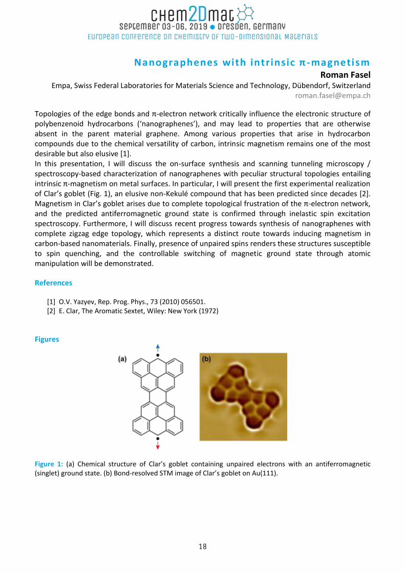
Topologies of the edge bonds and π-electron network critically influence the electronic structure of polybenzenoid hydrocarbons (‘nanographenes’), and may lead to properties that are otherwise absent in the parent material graphene. Among various properties that arise in hydrocarbon compounds due to the chemical versatility of carbon, intrinsic magnetism remains one of the most desirable but also elusive [1]. In this presentation, I will discuss the on-surface synthesis and scanning tunneling microscopy / spectroscopy-based characterization of nanographenes with peculiar structural topologies entailing intrinsic π-magnetism on metal surfaces. In particular, I will present the first experimental realization of Clar’s goblet (Fig. 1), an elusive non-Kekulé compound that has been predicted since decades [2]. Magnetism in Clar’s goblet arises due to complete topological frustration of the π-electron network, and the predicted antiferromagnetic ground state is confirmed through inelastic spin excitation spectroscopy. Furthermore, I will discuss recent progress towards synthesis of nanographenes with complete zigzag edge topology, which represents a distinct route towards inducing magnetism in carbon-based nanomaterials. Finally, presence of unpaired spins renders these structures susceptible to spin quenching, and the controllable switching of magnetic ground state through atomic manipulation will be demonstrated.
References
[1] O.V. Yazyev, Rep. Prog. Phys., 73 (2010) 056501. [2] E. Clar, The Aromatic Sextet, Wiley: New York (1972)
Figures
Figure 1: (a) Chemical structure of Clar’s goblet containing unpaired electrons with an antiferromagnetic (singlet) ground state. (b) Bond-resolved STM image of Clar’s goblet on Au(111).
18
Chemical Funct ionalizat ion of Graphene and Black Phosphorus Andreas Hirsch
Department of Chemistry and Pharmacy, University of Erlangen-Nuremberg Nikolaus-Fiebiger-Strasse 10, 91058 Erlangen, Germany
Chemical functionalization of new C-allotropes such as graphene is of fundamental interest and opens the door to unprecedented materials applications. We will report on the development of efficient functionalization protocols of this 2D-system using both covalent and non-covalent approaches. In particular the reductive functionalization of graphene allows for the attachment of a variety of functional systems such as porphyrines and fullerenes to the basal plane. Moreover, we will present first results on the chemical functionalization of other 2D-materials in particular black phosphorus (BP).
19
Properties of low-dimensional materials by high-resolution low-voltage and/or lo w-dose TEM
Ute Kaiser Central Facility of Materials Science Electron Microscopy, Ulm University, Albert Einstein Allee 11,
89081 City, Country [email protected]
Advanced two-dimensional materials have been identified as highly promising for next-generation electronic, optoelectronic, sensing and quantum devices. Thus, it is a growing demand to unravel the atomic and electronic structure and to understand their properties at the atomic scale. In this presentation, we report on the structure and properties of (1) pristine and electron-beam-functionalized two-dimensional inorganic materials of transition metal di- and tri-chalchogenide heterostructures [1-4], (2) on two-dimensional organic polyimine structures [5], on fundamental insight into (3) nucleation of metals [6], (4) metal bonding and (4) in-situ lithiation and delithiation processes between bilayer graphene [7].
For this purpose, a new type of transmission electron microscopes, the SALVE microscope, operating at electron accelerating voltages between 80kV and 20kV has been developed recently, which we will be briefly outline. It allows undercutting most of the materials electron-beam-induced knock-on damage thresholds and enables sub-Angstrom resolution down to 40kV by correcting not only the geometrical aberrations of the objective lens but also its chromatic aberration, allowing to study the dynamic of interactions in one 4kx4k image [8-10]. Electron-beam-induced radiolysis effects we reduced by optimized sample geometry. For imaging the organic polyimine structures, we
use 300kV imaging and reduce electron-beam-induced knock on damage effects with refined and optimized experimental design including low electron doses, optimized camera sampling and defocus.
DFT calculations we apply to understand and discover the defect’s properties.
References
[1] P. Börner, M. K. Kinyanjui, T. Börkmann, T. Lehnert, A. V. Krashenninikov, U. Kaiser, APL, 113 (2018) 173103
[2] M. K. Kinyanjui, J. Koester, F. Boucher, A. Wildes, and U. Kaiser, Phys. Rev. B 98 (2018), 035417 [3] T. Lehnert, M. Ghorbani-Asl, J. Köster, Z. Lee, A. V. Krasheninnikov, and U. Kaiser, ACS Appl. Nano
Mater. 2 (2019) 3262-3270 [4] M. K. Kinyanjui, T. Björkman, T. Lehnert, J. Köster, A. Krasheninnikov, U. Kaiser, Phys. Rev. B 99 (2019)
024101 [5] K. Liu, H. Qi, R. Dong, R. Shivhare, M. Addicoat, T Zhang, H. Sahabudeen, T. Heine, S. Mannsfeld, U.
Kaiser, Z. Zheng, X. Feng, Nature Chemistry accepted [6] [6] K. Cao, T. Zoberbier, J. Biskupek, A. Botos, R. L. McSweeney, A. Kurtoglu, C. T. Stoppiello, A. V.
Markevich, E. Besley, T. W. Chamberlain, U. Kaiser, A. N. Khlobystov, Nature Communications 9 (2018) 3382
[7] [7] M. Kühne, F. Börrnert, S. Fecher, M. Ghorbani-Asl, J. Biskupek, D. Samuelis, A. V. Krasheninnikov, U. Kaiser, J. H. Smet, Nature (2018) doi:10.1038/s41586-018-0754-2
[8] [8] U. Kaiser, J. Biskupek, J.C. Meyer, J. Leschner, L. Lechner, H. Rose, M. S.- Pollach, A.N. Khlobystov, P. Hartel, H. Müller, M. Haider, S. Eyhusen and G. Benner, Ultramicroscopy 111 (2011) 1239.
[9] M. Linck, P. Hartel, S. Uhlemann, F. Kahl, H. Müller, J. Zach, and M Haider, M. Niestadt and M. Bischoff, J. Biskupek, Z. Lee, T. Lehnert, F. Börrnert, H. Rose, and U. Kaiser, PRL 117 (2016) 076101.
[10] F. Börrnert and U. Kaiser Chromatic- and geometric-aberration-corrected TEM imaging at 80 kV and 20 kV Physical Review A 98 (2), 023861 (2018) 1.
20
Graphene Nanoribbons – Merging the (1D) Conjugated Polymer and (2D) Graphene Worlds
Klaus Müllen Max Planck Institute for Polymer Research, Mainz, Germany
Graphenes and graphene nanoribbons (GNRs), their geometrical cutouts, are exciting additions to the rich carbon family. Graphenes hold enormous promise, for example, in energy technologies and non-linear optics. However, before they can be employed in electronics and their high charge-carrier mobility be utilized in field-effect transistors (FETs), an opening of their band gaps must be achieved. The best answer to this longstanding problem are GNRs, and this brings precision polymer synthesis into play. While protocols from lithography or unzipping of carbon nanotubes offer no control over length, width and edge structure, bottom-up synthesis is the method of choice. We present unprecedented syntheses proceeding in, both, solution and on-surface. The latter approach, which can be scaled up by extension from UHV-conditions to chemical vapor deposition, also allows in-situ monitoring and proof of GNR-formation by scanning tunneling microscopy. Based on these material breakthroughs, we fabricate FETs from single GNRs and GNR-networks and compare the performance with that of conventional conjugated polymers. Surprisingly, the design of GNRs with appropriate combinations of arm-chair and zig-zag edges furnishes robust topological insulators in 2D as well as spin states with high correlation times. There is hope that these features provide entries into spintronics and even quantum computing.
References
[1] Science 2016, 351, 957; Nature 2016, 531, 489; J. Amer. Chem. Soc. 2018, 140, 9104; Angew. Chem. Int. Ed. 2018, 57, 11233; Nature 2018, 557, 557, 691; Nature Commun. 2018, 9(1); Nature 2018, 560, 209; Nature 2018, 561, 507.
21
Control led doping of 2D materia ls with responsive molecules Paolo Samorì
ISIS, University of Strasbourg & CNRS 8, allée Gaspard Monge
67000 Strasbourg (France) [email protected]
Abstract The already exceptional properties of 2D materials can be further tuned, enriched and
leveraged by interfacing them with ad hoc molecules, by mastering principle of
supramolecular chemistry. By taking full advantage of the almost unlimited variety of
molecules that can be designed and synthesized with functionalities at will, one can engineer
2D materials exhibiting dynamic physical and chemical properties, by imparting them novel
functions, with the ultimate goal of generating multifunctional hybrid systems for applications
in (opto)electronics, sensing and energy. [1]
In my lecture, I will review our recent findings on the use of non-covalent functionalization in
order to controllably dope different 2D materials including Graphene, MoS2, WSe2, BP by
exploiting the effect of either surface dipoles [2] or charge transfer [3] with the goal of
engineering artificial responsive hetero-structures.
Our approaches provide a glimpse on the chemist’s toolbox to generate multifunctional 2D
materials-based hybrids with ad-hoc properties to address key global challenges in
electronics, sensing and energy applications.
References
[1] For reviews: (a) S. Bertolazzi, M. Gobbi, Y. Zhao, C. Backes, P. Samorì, "Molecular chemistry approaches for tuning the properties of two-dimensional transition metal dichalcogenides", Chem. Soc. Rev. 2018 47, 6845-6888. (b) M. Gobbi, E. Orgiu, P. Samorì, "When 2D materials meet molecules: opportunities and challenges of hybrid organic/inorganic van der Waals heterostructures", Adv. Mater. 2018, 30, 1706103. (c) Y. Zhao, S. Ippolito, P. Samorì, "Functionalization of 2D materials with photosensitive molecules: from light-responsive hybrid systems to multifunctional devices", Adv. Opt. Mater. 2019 in press.
[2] For the use of molecular-dipole-induced shift in work function: (a) M. Gobbi, S. Bonacchi, J.X. Lian, A. Vercouter, S. Bertolazzi, B. Zyska, M. Timpel, R. Tatti, Y. Olivier, S. Hecht, M.V. Nardi, D. Beljonne, E. Orgiu, P. Samorì, "Collective molecular switching in hybrid superlattices for light-modulated two-dimensional electronics", Nat. Commun. 2018, 9, 2661. (b) M. Gobbi, S. Bonacchi, J. Lian, Y. Liu, X.-Y. Wang, M.-A. Stoeckel, M.A. Squillaci, G. D'Avino, A. Narita, K. Müllen, X. Feng, Y. Olivier, D. Beljonne, P. Samorì, E. Orgiu, "Periodic potentials in hybrid van der Waals heterostructures formed by supramolecular lattices on graphene", Nat. Commun. 2017, 8, 14767. (c) Y. Zhao, S. Bertolazzi, P. Samori, "A Universal Approach towards Light-Responsive Two-Dimensional Electronics: Chemically Tailored Hybrid van der Waals Heterostructures", ACS Nano, 2019, 13, 4814–4825.Authors, Journal, Issue (Year) page (Calibri 11)
[3] For the use of charge transfer: H. Qiu, Y. Zhao, Z. Liu, M. Herder, S. Hecht, P. Samorì, "Modulating the charge transport in two-dimensional semiconductors via energy level phototuning", 2019 submitted.
22

INVITED SPEAKERS
O p t o e l e c t r o n i c P r o c e s s e s i n C o v a l e n t O r g a n i c F r a m e w o r k s
Thomas Bein Department of Chemistry, University of Munich (LMU), 81377 Munich, Germany
Photoactive molecular building blocks can be spatially integrated into the crystalline lattice of covalent organic frameworks (COFs), allowing us to create models for organic bulk heterojunctions and porous electrodes for photoelectrochemical systems. In this presentation, we will address means of controlling the morphology and packing order of COFs in thin films [1] and with spatially locked-in building blocks.[2] We will discuss different strategies aimed at creating electroactive networks capable of light-induced charge transfer. For example, we have developed a COF containing stacked thienothiophene-based building blocks acting as electron donors with a 3 nm open pore system, which showed light-induced charge transfer to an intercalated fullerene acceptor phase.[3] Contrasting this approach, we have designed a COF integrated heterojunction consisting of alternating columns of stacked donor and acceptor molecules, promoting the photo-induced generation of mobile charge carriers inside the COF network.[4] Additional synthetic efforts have led to several COFs integrating extended chromophores capable of efficient harvesting of visible and near infrared light, for example [5]. Extending newly developed thin film growth methodology to a solvent-stable oriented 2D COF photoabsorber structure, we have recently established the capability of COF films to serve in photoelectrochemical water splitting systems.[6] Related COF films can also act as ultrafast solvatochromic chemical sensors.[7] The great structural diversity and morphological precision that can be achieved with COFs make these materials intriguing model systems for organic optoelectronic materials. References
[1] D.D. Medina, J.M. Rotter, Y.H. Hu, M. Dogru, V. Werner, F. Auras, J.T. Markiewicz, P. Knochel, T. Bein, Journal of the American Chemical Society, 137 (2015) 1016-1019.
[2] L. Ascherl, T. Sick, J.T. Margraf, S.H. Lapidus, M. Calik, C. Hettstedt, K. Karaghiosoff, M. Doblinger, T. Clark, K.W. Chapman, F. Auras, T. Bein, Nature Chemistry, 8 (2016) 310-316.
[3] M. Dogru, M. Handloser, F. Auras, T. Kunz, D. Medina, A. Hartschuh, P. Knochel, T. Bein, Angewandte Chemie-International Edition, 52 (2013) 2920-2924.
[4] M. Calik, F. Auras, L.M. Salonen, K. Bader, I. Grill, M. Handloser, D.D. Medina, M. Dogru, F. Lobermann, D. Trauner, A. Hartschuh, T. Bein, Journal of the American Chemical Society, 136 (2014) 17802-17807.
[5] N. Keller, D. Bessinger, S. Reuter, M. Calik, L. Ascherl, F.C. Hanusch, F. Auras, T. Bein, Journal of the American Chemical Society, 139 (2017) 8194-8199.
[6] T. Sick, A.G. Hufnagel, J. Kampmann, I. Kondofersky, M. Calik, J.M. Rotter, A. Evans, M. Doblinger, S. Herbert, K. Peters, D. Bohm, P. Knochel, D.D. Medina, D. Fattakhova-Rohlfing, T. Bein, Journal of the American Chemical Society, 140 (2018) 2085-2092.
[7] L. Ascherl, E.W. Evans, M. Hennemann, D. Di Nuzzo, A.G. Hufnagel, M. Beetz, R.H. Friend, T. Clark, T. Bein, F. Auras, Nature Communications, 9 (2018).
24
Multi functional biodegradable graphene -based materials for cancer therapy
Alberto Bianco University of Strasbourg, CNRS, Immunology, Immunopathology and Therapeutic Chemistry,
UPR3572, Strasbourg, France [email protected]
Graphene-based nanomaterials are considered unique systems for many applications in different fields including biomedicine [1]. They are offering the possibility of original chemical functionalization and design of complex multifunctional systems that allow further their exploitation in therapy, imaging and diagnosis [2]. In this lecture, I will present the chemical strategies to functionalize graphene-based nanomaterials with appropriate functional groups and therapeutic molecules in view of their biomedical applications. I will present few examples of their use in cancer therapy and imaging [3, 4]. I will also describe how it is possible to enhance the biodegradability and tune the toxic effects of these different materials [1]. References
[1] Martìn, C., Kostarelos, K., Prato M., Bianco, A. Chem. Commun. 55 (2019) 5540-5546 [2] Reina, G., González-Domínguez, J. M., Criado, A., Vázquez, E., Bianco, A., Prato, M. Chem. Soc. Rev. 46
(2017) 4400-4416 [3] Reina, G., Ruiz, A., Murera, D., Nishina, Y., Bianco, A. ACS Appl. Mater. Interfaces 11 (2019) 7695-7702 [4] Martín, C., Ruiz, A., Keshavan, S., Reina, G., Murera, D., Nishina, Y., Fadeel, B., Bianco, A. (2019)
submitted
25
Liquid phase production of 2D crystals for energy applicat ions
Francesco Bonaccorso Istituto Italiano di Tecnologia, Graphene Labs, Via Morego 30, Genova, Italy
BeDimensional SpA, Via Albisola 121, Genova, Italy [email protected]
Two-dimensional (2D) materials are entering several application areas,[1-5] improving the performance of existing devices or enable new ones.[1-5] A key requirement for the implementation of 2D materials in the energy field is the development of industrial-scale, reliable, inexpensive production processes,[2] while providing a balance between ease of fabrication and final product quality. In this context, the production of 2D materials by solution processing[2,6] represents a simple and cost-effective pathway towards the development of 2D materials-based energy devices, presenting huge integration flexibility compared to other production methods. Here, I will first present our strategy to produce 2D materials on large scale by wet-jet milling[7] of their bulk counterpart and then an overview of their applications for energy devices.[3,8-15] . References
1. A. C. Ferrari, F. Bonaccorso, et al., Nanoscale, 7, 4598-4810 (2015). 2. F. Bonaccorso, et al., Materials Today, 15, 564-589, (2012). 3. F. Bonaccorso, et. al., Nature Photonics 4, 611-622, (2010). 4. F. Bonaccorso, Z. Sun, Opt. Mater. Express 4, 63-78 (2014). 5. G. Iannaccone, et al., Nature Nanotech 13, , 183, (2018). 6. F. Bonaccorso, et. al., Adv. Mater. 28, 6136-6166 (2016). 7. A. E. Del Rio Castillo et. al., Mater. Horiz. 5, 890 (2018). 8. F. Bonaccorso, et. al.,. Science, 347, 1246501 (2015). 9. J. Hassoun, et al. Nano Lett. 14, 4901-4906 (2014). 10. F. Bonaccorso, et al. Adv. Funct. Mater. 25, 3870-3880 (2015). 11. F. Biccari, et al. Adv. Energy Mater. 7, 1701349 (2017). 12. A. Agresti, et al. ACS Energy Letters 4, 1862-1871 (2019). 13. A. Capasso, et al. Adv. Ener. Mater. 6, 1600920, (2016). 14. L. Najafi, et al. ACS Nano 12, 10736 (2018). 15. S. Bellani et al., Advanced Functional Materials 29, 1807659 (2019).
26
Water-based 2D-Inks: from al l - inkjet printed devices to biomedical appl ications
Cinzia Casiraghi School of chemistry, University of Manchester, M139PL, UK
Solution processing of graphene [1] allows simple and low-cost techniques, such as ink-jet printing [2,3] to be used for fabrication of heterostructure-based devices of arbitrary complexity. However, the success of this technology is determined by the nature and quality of the inks used. In this talk I will show a general formulation engineering approach to achieve highly concentrated, printable and water-based 2D crystal formulations, which also provide optimal film formation for multi-stack fabrication [4]. Examples of all-inkjet printed heterostructures, such as large area arrays of photosensors on plastic [4], programmable logic memory devices [4], capacitors [5] and transistors [6], will be discussed. Cytotoxicity tests confirm biocompatibility of the 2D inks [4] allowing possible use of the material for biomedical applications. However, the graphene inks are anionic, while positively charged nanomaterials are known to better interact with the biological environment (e.g. cell membrane, siRNA, etc). If time allows, I will show production of cationic graphene dispersions, suitable for biomedical applications, by using ad-hoc designed stabilisers [7,8].
References
1. Coleman et al, science 331, 568 (2011) 2. Torrisi et al, ACS Nano, 6, 2992 (2012) 3. Finn et al, J. Mat. Chem C 2, 925 (2014) 4. McManus et al, Nature Nano, 12, 343 (2017) 5. Worsley et al, ACS Nano, 2018, DOI: 10.1021/acsnano.8b06464 6. Lu et al, under review 7. Shin et al, Mol. Syst. Des. Eng., 2019, DOI:10.1039/C9ME00024K 8. Shin et al, under review
27
2D-based composites as battery electrodes Jonathan N Coleman, Sang-Hoon park, Ruiyuan Tian, Joao Coelho, Andrew Harvey,
Aideen Griffin, Valeria Nicolosi, Christopher Benndorf*, Oliver Oeckler* AMBER Research centre, Trinity College Dublin, D2, Ireland.
*Institut für Mineralogie, Kristallographie und Materialwissenschaft, Scharnhorststr. 20, Universität Leipzig, Germany
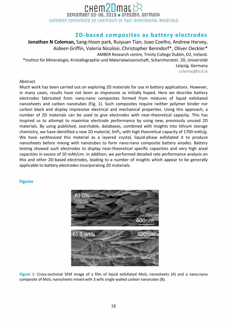
Abstract Much work has been carried out on exploring 2D materials for use in battery applications. However, in many cases, results have not been as impressive as initially hoped. Here we describe battery electrodes fabricated from nano:nano composites formed from mixtures of liquid exfoliated nanosheets and carbon nanotubes (Fig. 1). Such composites require neither polymer binder nor carbon black and display impressive electrical and mechanical properties. Using this approach, a number of 2D materials can be used to give electrodes with near-theoretical capacity. This has inspired us to attempt to maximize electrode performance by using new, previously unused 2D materials. By using published, searchable, databases, combined with insights into lithium storage chemistry, we have identified a new 2D material, SnP3, with high theoretical capacity of 1700 mAh/g. We have synthesized this material as a layered crystal, liquid-phase exfoliated it to produce nanosheets before mixing with nanotubes to form nano:nano composite battery anodes. Battery testing showed such electrodes to display near-theoretical specific capacities and very high areal capacities in excess of 10 mAh/cm. In addition, we performed detailed rate performance analysis on this and other 2D-based electrodes, leading to a number of insights which appear to be generally applicable to battery electrodes incorporating 2D materials.
Figures
Figure 1: Cross-sectional SEM image of a film of liquid exfoliated MoS2 nanosheets (A) and a nano:nano composite of MoS2 nanosheets mixed with 3 wt% single walled carbon nanotubes (B).
28
Going beyond copper: wafer -scale synthesis of graphene on sapphire
Camilla Coletti Istituto Italiano di Tecnologia, P.zza San Silvestro 12, 56127 Pisa, Italy
The adoption of graphene in electronics, optoelectronics and photonics is hindered by the difficulty in obtaining high quality material on technologically-relevant substrates, over wafer-scale sizes and with metal contamination levels compatible with industrial requirements. To date, the direct growth of graphene on insulating substrates has proved to be challenging, usually requiring metal-catalysts or yielding defective graphene. In this work, we demonstrate a metal-free approach implemented in commercially available reactors to obtain high-quality monolayer graphene on c-plane sapphire substrates via chemical vapour deposition (CVD). Raman spectroscopy and electrical transport measurements reveal high quality graphene with mobilities consistently above 2000 cm2/Vs. We scale up the process to 4-inch and 6-inch wafer sizes and demonstrate that metal contamination levels are within the limits for back-end-of-line (BEOL) integration. The growth process introduced here establishes a method for the synthesis of wafer-scale graphene films on a technologically viable basis. References
[1] N. Mishra et al., https://arxiv.org/abs/1907.01610
Acknowledgments
The research leading to these results has received funding from the European Union’s Horizon 2020 research and innovation program under grant agreement No.785219 – GrapheneCore2.
29
Periodic Non-Covalent and Covalent Functionalizat ion of 2D Materials
Steven De Feyter KU Leuven, Department of Chemistry, Celestijnenlaan 200F, B-3001 Leuven, Belgium
In this presentation, I will focus on the functionalization of graphite, graphene, and transition metal transition metal dichalcogenides (TMDs) using two approaches [1]. A first approach is based on the formation of self-assembled molecular networks (SAMNs) at the interface between a liquid or air, and the solid substrate. I will discuss concepts of nanostructuring emphasizing the effect of solvent, solute concentration and temperature, stimulus-driven self-assembly and self-assembly under nanoconfinement conditions. A second approach is based on grafting molecules on these substrates via covalent chemistry. In addition to a discussion on the functionalization principles, different approaches to nanostructure these surfaces, both bottom-up as top-down, will be demonstrated [2-5]. Advanced interface specific methods such as scanning tunnelling microscopy (STM) and atomic force microscopy (AFM) provide structural and other types of information at the nanoscopic level. Various applications will be presented, including multilayered growth, sensing, and molecule modified graphene field effect transistors [6,7].
References
[1] L. Daukiya, J. Seibel, S. De Feyter, Advance in Physics: X, 2019, in press [2] Z. Li, H. Van Gorp, P. Walke, T. H. Phan, Y. Fujita, J. Greenwood, O. Ivasenko, K. Tahara, Y. Tobe, H. Uji-
i, S. F. L. Mertens, S. De Feyter, Nanoscale, 9 (2017) 5188 [3] H. Van Gorp, P. Walke, A. M. Bragança, J. Greenwood, O. Ivasenko, B. Hirsch, S. De Feyter, ACS Applied
Materials & Interfaces, 10 (2018) 12005 [4] K. Tahara, T. Ishikawa, B. E. Hirsch, Y. Kubo, A. Brown, S. Eyley, L. Daukiya, W. Thielemans, Z. Li, P.
Walke, S. Hirose, S. Hashimoto, S. De Feyter, Y. Tobe, ACS Nano, 12 (2018) 11520 [5] T. H. Phan, H. Van Gorp, Z. Li, T. M. T. Huynh, Y. Fujita, L. Verstraete, S. Eyley, W. Thielemans, H. Uji-i,
B. E. Hirsch, S. F. L. Mertens, J. Greenwood, O. Ivasenko, S. De Feyter, ACS Nano, DOI: 10.1021/acsnano.9b00439
[6] R. Phillipson, C. J. Lockhart de la Rosa, J. Teyssandier, P. Walke, D. Waghray, Y. Fujita, J. Adisoejoso, K. S. Mali, I. Asselberghs, C. Huyghebaert, H. Uji-i, S. De Gendt, S. De Feyter, Nanoscale, 8 (2016) 20017
[7] G. Velpula, R. Phillipson, J. X. Lian, D. Cornil, P. Walke, K. Verguts, S. Brems, H. Uji-i, S. De Gendt, D. Beljonne, R. Lazzaroni, K. S. Mali, S. De Feyter, ACS Nano, 13 (2019) 3512
Figures
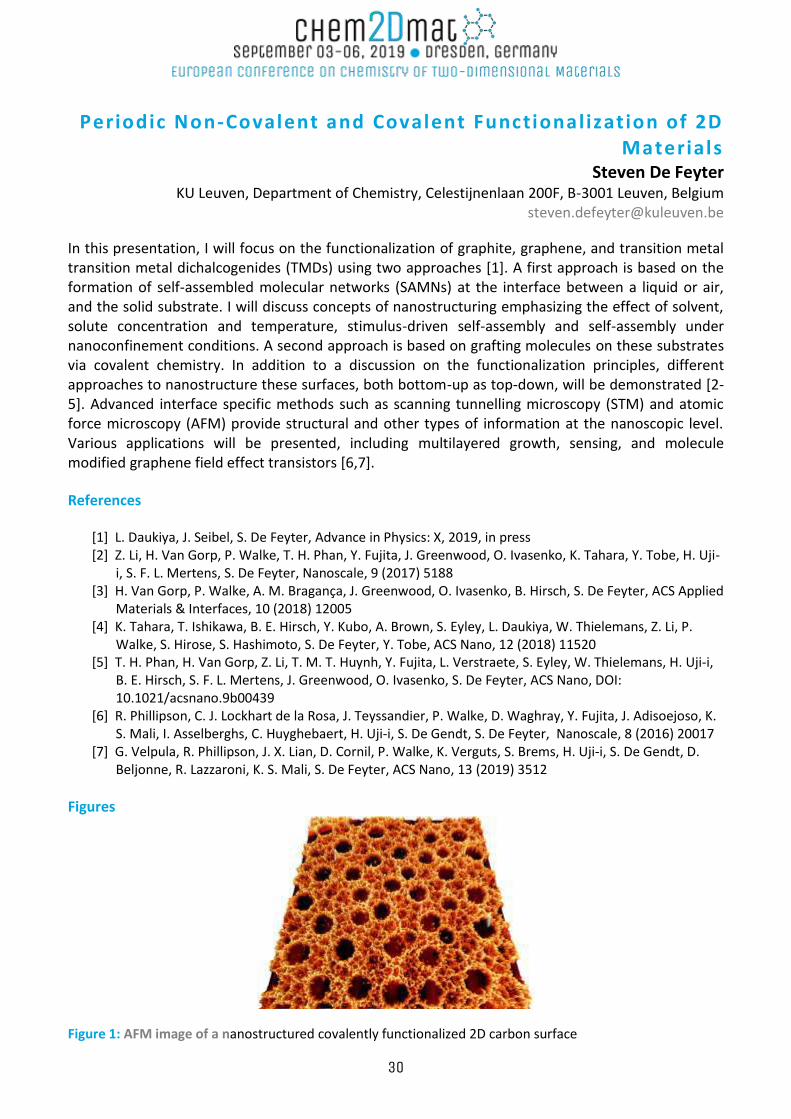
Figure 1: AFM image of a nanostructured covalently functionalized 2D carbon surface
30
Electronic-Structure Engineering of Graphene by Semiconductor Intercalation
Shixuan Du1, Yu-Yang Zhang1, Yixuan Gao1, Geng Li1, Lizhi Zhang1, Sokrates T. Pantelides2,1, and Hong-Jun Gao1
1. Institute of Physics & University of Chinese Academy of Sciences, CAS, Beijing, China, 100049 2. Vanderbilt University, Nashville, Tennessee, USA, 37240
The epitaxial growth of graphene on transition-metal substrates has proved to be an efficient method to synthesize high-quality large-area graphene. However, due to the interaction between graphene and the transition-metal substrate, the electronic structure of the as-fabricated graphene is distorted. Here, using density functional theory calculations, we investigated the effect of intercalating two-dimensional (2D) silicon and III–V materials, such as double-layer honeycomb AlAs, into the graphene-metal interface. We found that the intercalation of these 2D materials significantly reduces the interaction between graphene and the transition-metal substrate. The Dirac state is largely restored. The doping level of graphene induced by the 2D intercalated material and the metal substrate is proportional to the work function difference between graphene and 2D materials/metal. We carried out a controlled experiment to intercalate silicon into the epitaxial graphene on Ru(0001). By controlling the amount of silicon, ordered arrays of nano flakes as well as single layers and multilayers of silicene can be successfully fabricated between graphene and Ru(0001). Density functional theory calculations show weak interactions between graphene and silicene layers. In addition, the as-fabricated graphene/silicene heterostructures show no observable damage after air exposure for extended periods, indicating good air stability. The I–V characteristics of the vertical graphene/silicene/Ru heterostructures show rectification behavior [1, 2].
References
[1] G. Li, et al., Adv. Mater. 30, 1804650, (2018). [2] Y. Gao, Y.-Y. Zhang, S. Du. J. Phys. Condens. Matter 31, 194001, (2019)
31
Funct ional isat ionStrategies of Monolayer Surfaces GeorgS.Duesberg,RitaSiris*,LauraHöltgen*,KanghoLee*,JohnMcManus#,ConorCullen#,Hyun-JeongKim#,SiweiLuo*,CorinnaWeiss+,FrankHauke+,AndreasHirsch+
*UniversitätderBundeswehrMünchen,Werner-Heisenberg-Weg39,85577Neubiberg,Germany
#SchoolofChemistry,TrinityCollegeDublin,CollegeGreen,Dublin2,Ireland+InstitutfürOrganischeChemie,Henkestr.42,91054Erlangen,Germany
Two-dimensional(2D)materialssuchasgrapheneandtransitionmetaldichalcogenides(TMDs)areintensively investigatedbecauseof their uniqueproperties. The finding of thickness dependbandgaps and high carrier mobility make them highly sought for fundamental studies and emergingapplications in electronics. For most of those applications modification and passivation of themonolayersviafunctionalisationisaprerequisite.Asthegasphasesynthesismethods-preferablefor electronical applications - yield substrate bound monolayers, wet-chemical functionalisationroutes are somehow limited. In this presentation, various covalent and non-covalent routes areinvestigatedtoyieldon-chipfunctionalisationofmonolayer2Dmaterials.ThegrapheneandTMDsfilms are grown by chemical vapor deposition CVD, which yields a high surface coverage withmonolayers. Thenon-covalent functionalisationapproach is viaphysisorptionofperylenebisimidemolecules from the liquid phase. As a result self-assembledmonolayers (SAMs) through van derWaals interactions are created. By using a number of derivatives of perylene bisimides, welldefined, stable surface functionalisation is realised.1,2 Additionally, results on remote plasmatreatmentsofgrapheneandMoS2,introducingheteroatomswillbebrieflypresented.3Thesurfacesof the pristine and functionalised films are comprehensively are investigated by Ramanspectroscopy,XPS,scanningprobetechniquesandTOF-SIMS.TheeffectontheelectronicpropertiesofthemonolayeronFETstructuresarediscussed. References[1] Berner,N.C.etal.UnderstandingandoptimisingthepackingdensityofperylenebisimidelayersonCVD-growngraphene.Nanoscale7,16337–42(2015).[2] Kim,H.etal.Optimizedsingle-layerMoS2field-effecttransistorsbynon-covalentfunctionalisation.Nanoscale10,17557–17566(2018).[3] McManus,J.B.etal.ControllingDefectandDopantConcentrationsinGraphenebyRemotePlasmaTreatments.Phys.StatusSolidiB254,(2017). Figures
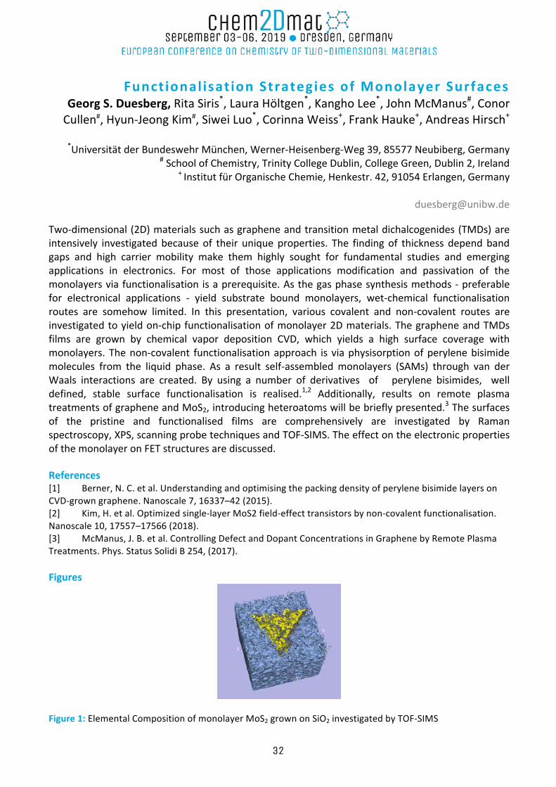
Figure1:ElementalCompositionofmonolayerMoS2grownonSiO2investigatedbyTOF-SIMS
32
‘Electronic structure and charge transport simulations in GRM-organic hybrids: Where Chemistry meets Physics'
Sai Manoj Gali University of Mons, Place du Parc 20, 7000 Mons
Abstract The electronic structure of 2D materials can be profoundly affected by physical or chemical adsorption of (electro-active) conjugated molecules. The presence of adlayers manifests as changes in the work function and electrical doping and can be used to tune charge carrier mobility and conductivity. In this talk, we will review recent first-principles simulations performed in our group to model:
(i) The doping of monolayer transition metal dichalcogenies via physisorption of aromatic solvent molecules [1]. (ii) The control of charge carrier density in superlattices formed by photochromic molecules self-assembled on graphene [2]. (iii) The engineering and healing of chemically active defects in monolayer MoS2 [3]. (iv) The charge transport in photoswitchable self-assembled monolayers organic-graphene hybrids [4].
References
[1] Y. Wang et al. J. Phys. Chem. Lett. 10 (2019) 540-547. [2] M. Gobbi et al. Nature Communications 9 (2018) 2661. [3] S. Bertolazzi et al. Advanced Materials 29 (2017) 1606760. [4] C. Tonnelé et al., JPhysMaterials, in press.
Figures
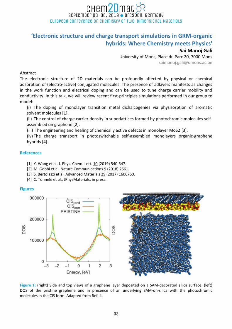
Figure 1: (right) Side and top views of a graphene layer deposited on a SAM-decorated silica surface. (left) DOS of the pristine graphene and in presence of an underlying SAM-on-silica with the photochromic molecules in the CIS form. Adapted from Ref. 4.
33
Charge and gas transport in complex 2-dimensional anisotropic systems
Vincenzo Palermo, Andrea Liscio, Alessandro Kovtun, Marco Affronte, Andrea Candini National Research Council (CNR-ISOF), Bologna, Italy
Chalmers University of Technology, Gothenburg, Sweden Università di Modena e Reggio Emilia, Modena, Italy
Applications of graphene and 2D materials (2DM) in electronics or composites require to study charge transport in complex systems, i.e. mesoscopic layers made of billions of stacked nanosheets. In this case, the material’s electrical conductivity depends strongly on the flake-flake interaction, and on the flake size. Besides charge transport along the plane, permeation of small molecules across the plane is also important for applications, as example, in packaging (gas barrier) or in water purification. Also, in this case, the stacking and the interaction of the different nanosheets with each other will influence strongly the transport mechanism. Here, we give an overview of our results recently obtained to tackle this challenging problem, in particular related to:
Charge transport studies in composite, polydisperse 2DM systems, based on different regimes, from Arrhenius-like behavior to variable range hopping.[1]
Gas transport studies in composite, polydisperse 2DM systems featuring selective permeation for different gases of industrial interest.[2]
Statistical modelling of flake size distribution in 2D materials, for fundamental study or benchmarking of commercial products.[3-5]
Overall, this approach shall help to bridge the gap between studies performed at fundamental level on single monoatomic sheets, and complex behaviour observed in realistic composite materials.
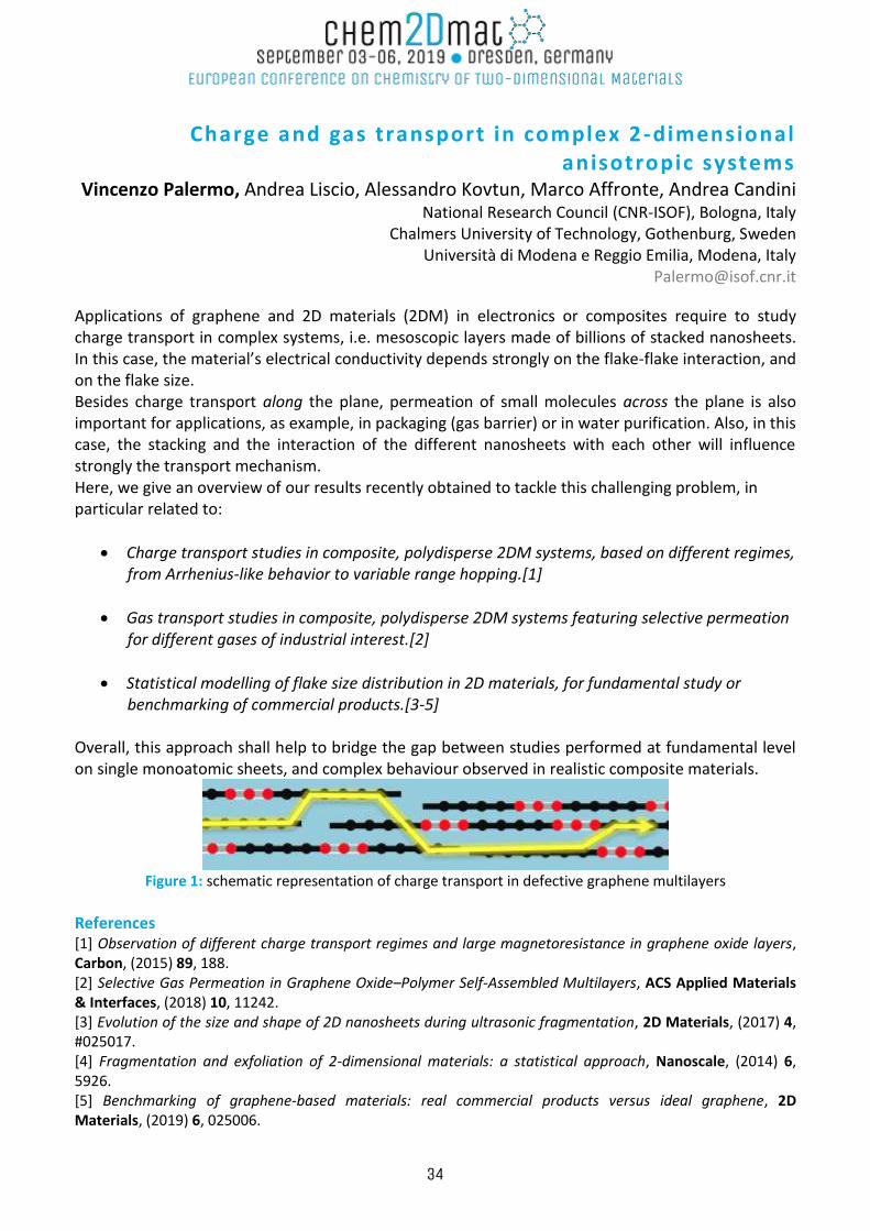
Figure 1: schematic representation of charge transport in defective graphene multilayers
References [1] Observation of different charge transport regimes and large magnetoresistance in graphene oxide layers, Carbon, (2015) 89, 188. [2] Selective Gas Permeation in Graphene Oxide–Polymer Self-Assembled Multilayers, ACS Applied Materials & Interfaces, (2018) 10, 11242. [3] Evolution of the size and shape of 2D nanosheets during ultrasonic fragmentation, 2D Materials, (2017) 4, #025017. [4] Fragmentation and exfoliation of 2-dimensional materials: a statistical approach, Nanoscale, (2014) 6, 5926. [5] Benchmarking of graphene-based materials: real commercial products versus ideal graphene, 2D Materials, (2019) 6, 025006.
34
Design of Crystalline 2D Materials: The SURMOF Approach
Christof Wöll Institute of Functional Interfaces (IFG), Karlsruhe Institute of Technology, North Campus,76021
Karlsruhe, FRG [email protected]
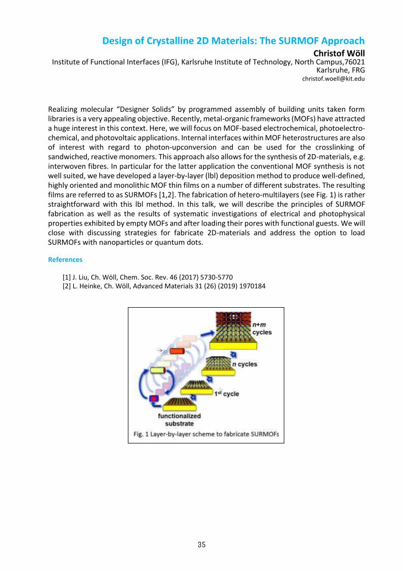
Realizing molecular “Designer Solids” by programmed assembly of building units taken form libraries is a very appealing objective. Recently, metal-organic frameworks (MOFs) have attracted a huge interest in this context. Here, we will focus on MOF-based electrochemical, photoelectro-chemical, and photovoltaic applications. Internal interfaces within MOF heterostructures are also of interest with regard to photon-upconversion and can be used for the crosslinking of sandwiched, reactive monomers. This approach also allows for the synthesis of 2D-materials, e.g. interwoven fibres. In particular for the latter application the conventional MOF synthesis is not well suited, we have developed a layer-by-layer (lbl) deposition method to produce well-defined, highly oriented and monolithic MOF thin films on a number of different substrates. The resulting films are referred to as SURMOFs [1,2]. The fabrication of hetero-multilayers (see Fig. 1) is rather straightforward with this lbl method. In this talk, we will describe the principles of SURMOF fabrication as well as the results of systematic investigations of electrical and photophysical properties exhibited by empty MOFs and after loading their pores with functional guests. We will close with discussing strategies for fabricate 2D-materials and address the option to load SURMOFs with nanoparticles or quantum dots.
References
[1] J. Liu, Ch. Wöll, Chem. Soc. Rev. 46 (2017) 5730-5770 [2] L. Heinke, Ch. Wöll, Advanced Materials 31 (26) (2019) 1970184
35

INVITED SPEAKERS (parallel workshops)
Future applicat ions for 2D materials: the immune system scenario
Lucia Gemma Delogu University of Padua, Via Ugo Bassi, 58/B
35131 a, Padua, Italy [email protected]
Graphene and other 2D materials are opening new markets and even replacing existing technologies thanks to their amazing chemical and physical properties. An ever-growing number of graphene and 2D-enhanced products are already commercially available. However, despite the large efforts and an impressive number of research projects funded in Europe and worldwide, a “killer application” of 2D materials is not yet universally recognized. What would happen if the future killer application of 2D materials arose from cell biology and immunology, the most unexpected fields for material scientists? Our expertise on the immune system interaction with nanomaterials is focusing on this key aspect of 2D material properties. The overall objective of our research group is to provide new insights on 2D materials immune system interactions and identify highly biocompatible nanomaterials with specific functionalizations. We here will share published and unpublished data on different pictures of graphene, graphene nanoribbons and other nanomaterials, e.g. from cancer therapy to bone regeneration. In this talk I will provide key concepts aimed at transforming the current approach of 2D-based materials production, by shaping their chemical and physical parameters, on the basis of their intrinsic immune properties for a new application scenario.
References 1 Single cell mass cytometry reveals the impact of graphene on human primary immune cells Orecchioni M, Bedognetti D, Newman L, Fuoco C, Spada F, Hendrickx W, Marincola FM, Sgarrella F, Rodrigues FA, Ménard-Moyon C, Cesareni G, Kostarelos K, Bianco A and Delogu LG. Nature Communication 2017 2 Few-Layer Graphene Kills Selectively Tumor Cells from Myelomonocytic Leukemia Patients. Russier R, Léon V, Orecchioni M, Hirata E, Virdis P, Fozza C, Sgarrella F, Cuniberti G, Prato M, Vazquez E, Bianco A and Delogu LG. Angew. Chem. 2017 3 Molecular and Genomic Impact of Large and Small Lateral Dimension Graphene Oxide Sheets on Human Immune Cells from Healthy Donors. Orecchioni M, Jasim DA, Pescatori M, Manetti R, Fozza C, Sgarrella F, Bedognetti D, Bianco A, Kostarelos K and Delogu LG. Adv Healthc Mater. 2016 4 Graphene as cancer theranostic tool: progress and future challenges. Orecchioni M, Cabizza R, Bianco A, Delogu LG. Theranostics. 2015 5 Impact of carbon nanotubes and graphene on immune cells. Orecchioni M, Bedognetti D, Sgarrella F, Marincola FM, Bianco A, Delogu LG. J Transl Med. 2014 6 Stimulation of bone formation by monocyte-activator functionalized graphene oxide in vivo. Bordoni et al. Accepted 7 Grahene nanoribbons: bio and immune compatibility large scale screening on human immune cells. Fusco et al. in submission
37
Oxo-Graphene – Synthesis and Heterostructures Siegfried Eigler
Freie Universität Berlin, Takustraße 3, Berlin, Germany [email protected]
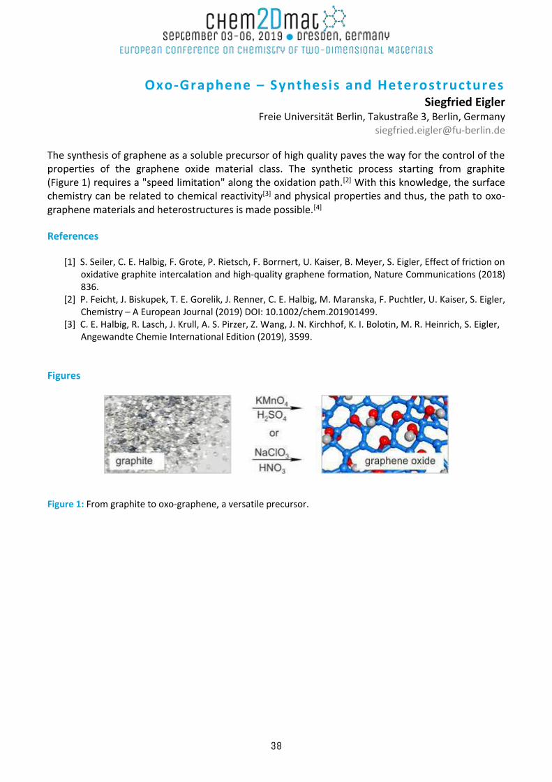
The synthesis of graphene as a soluble precursor of high quality paves the way for the control of the properties of the graphene oxide material class. The synthetic process starting from graphite (Figure 1) requires a "speed limitation" along the oxidation path.[2] With this knowledge, the surface chemistry can be related to chemical reactivity[3] and physical properties and thus, the path to oxo-graphene materials and heterostructures is made possible.[4]
References
[1] S. Seiler, C. E. Halbig, F. Grote, P. Rietsch, F. Borrnert, U. Kaiser, B. Meyer, S. Eigler, Effect of friction on oxidative graphite intercalation and high-quality graphene formation, Nature Communications (2018) 836.
[2] P. Feicht, J. Biskupek, T. E. Gorelik, J. Renner, C. E. Halbig, M. Maranska, F. Puchtler, U. Kaiser, S. Eigler, Chemistry – A European Journal (2019) DOI: 10.1002/chem.201901499.
[3] C. E. Halbig, R. Lasch, J. Krull, A. S. Pirzer, Z. Wang, J. N. Kirchhof, K. I. Bolotin, M. R. Heinrich, S. Eigler, Angewandte Chemie International Edition (2019), 3599.
Figures
Figure 1: From graphite to oxo-graphene, a versatile precursor.
38
Tailoring the properties of inorganic two -dimensional materials by post -synthesis introduction of impurit ies and
defects Arkady V. Krasheninnikov
Helmholtz Zentrum Dresden-Rossendorf, Institute of Ion Beam Physics and Materials Research,
Dresden, Germany [email protected]
Following isolation of a single sheet of graphene, many other 2D systems such as hexagonal BN, transition metal dichalcogenides (TMDs) or silica bilayers were manufactured. All these systems contain defects and impurities, which frequently govern the electronic and optical properties of these materials. Moreover, due to the very morphology of the 2D materials, which consist of essentially surface only, defects can easily be created by chemical treatment or irradiation, so that the properties of the materials can be tuned. For example, single impurities can be introduced by ion implantation or atom deposition, and when their concentration increases, a 2D alloy can be manufactured. Likewise, increasing vacancy concentration by sputtering atoms from a 2D TMD sheet can change the stoichiometry of the system and give rise to new features like inversion domains and grain boundaries or even new phases. In my talk, I will present the results [1-4] of our recent first-principles theoretical studies carried out with several experimental groups of how defects and impurities can be used to tailor properties of 2D materials or induce phase transformations in these systems. References
[1] T. Lehnert, M. Ghorbani-Asl, J. Köster, Z. Lee, A.V. Krasheninnikov, and U. Kaiser ACS Appl. Nano Mater. 2 (2019) 3262.
[2] P. M. Coelho, H.-P. Komsa, K. Lasek, V. Kalappattil, J. Karthikeyan, M.-H. Phan, A.V Krasheninnikov, and M. Batzill, Adv. El. Mater. 5 (2019) 1900044.
[3] J. Karthikeyan, H.-P. Komsa, M. Batzill, and A.V. Krasheninnikov, Nano Letters (2019). [4] R. Kozubek, M. Tripathi, M. Ghorbani-Asl, S. Kretschmer, L. Madauß, E. Pollmann, M. O’Brien, N.
McEvoy, U. Ludacka, T. Susi, G.S. Duesberg, R.A. Wilhelm, A. V. Krasheninnikov, J. Kotakoski, and M. Schleberger, J. Phys. Chem. Lett. 10 (2019) 904.
39
Merging Twisted Aromatics and Framework Materials Aurelio Mateo-Alonso (Koke)
1 POLYMAT, University of the Basque Country UPV/EHU. San Sebastián, 20018, Spain 2 Ikerbasque, Basque Foundation for Science. Bilbao, Spain
Polycyclic aromatic hydrocarbons (PAHs) are receiving a great deal of attention because of their increasing performance in organic electronic applications.[1] In general, PAHs are planar structures but they can adopt twisted conformations as the result of the steric strain induced by overcrowding or congestion in key positions of the aromatic core. Distorted PAHs have shown enhanced solubility and unique optoelectronic and chiroptical properties as an effect of their distorted molecular structure. We have implemented several strategies that provide access to distorted PAHs into the preparation of non-planar organic frameworks.[2,3,4] The most recent advances of these distorted 2D materials including synthetic routes, optoelectronic properties, self-organising properties, and potential applications will be discussed.
References
[1] A. Mateo-Alonso Chem. Soc. Rev., 43, (2014), 6311-6324. [2] S. More, S. Choudhary, A. Higelin, I. Krossing, M. Melle-Franco, A. Mateo-Alonso Chem. Comm., 50,
(2014), 1976-1979. [3] S. Choudhary, C. Gozalvez, A. Higelin, I. Krossing, M. Melle-Franco, A. Mateo-Alonso Chem. Eur. J., 20,
(2014), 1525-1528. [4] 4. A. B. Marco, D. Cortizo-Lacalle, I. Perez-Miqueo, G. Valenti, A. Boni, J. Plas, S. De Feyter, F.
Paolucci, M. Montes, A. Khlovystov, M. Melle-Franco and A. Mateo-Alonso Angew. Chem. Int. Ed., 56, (2017), 6946 –6951.
40
Phase engineering of col lo idal TMDs for eff ic ient electrocatalytic HER
Cecilia Mattevi ,
Imperial College London, Department of Materials, London, SW7 2AZ, UK
[email protected] Layered transition metal dichalcogenides (TMDs) display a variety of structural polymorphs defined by the symmetry of transition metal coordination polyhedra. Tailoring the lattice symmetry within individual TMD layers enables to achieve very different electronic properties ranging from semiconducting (2H phase) to metallic and semimetallic (1T/1T’ phases) with the same material composition. Exhibiting metallic behaviour, the metastable 1T’ phases are particularly appealing for the heterogeneous catalysis as they demonstrate the enhanced catalytic activity compared to the semiconducting 2H counterparts. The direct synthesis of the metastable phases of high purity and in measurable quantities remains challenging. Here, we present our work on the bottom-up synthesis of the metastable 1T’ phase of WSe2 based on the reaction between molecular precursors in liquid phase [1]. We design a kinetically-controlled bottom-up synthesis from molecular precursors to enable the formation of the metastable phase. We further demonstrate that the 1T’ phase is stable up to 400 oC and it is convertible into the semiconducting 2H phase at higher temperatures, making it suitable for a wide range of applications. The 1T’ WSe2 nanosheets exhibit a metallic nature evidenced by an enhanced electrocatalytic activity for hydrogen evolution reaction as compared to the 2H WSe2 and different sulphides. Further, we demonstrate how this synthesis approach can be applied to the synthesis of the 1T’/2H mixed-phase WxMo1-xSe2 (x = 0-1) with the aim of further enhancing the electrocatalytic activity for hydrogen evolution. References [1] M. S. Sokolikova, P. C. Sherrell, P. Palczynski, V. L. Bemmer and C. Mattevi, Nat. Commun., 2019, 10, 712.
41
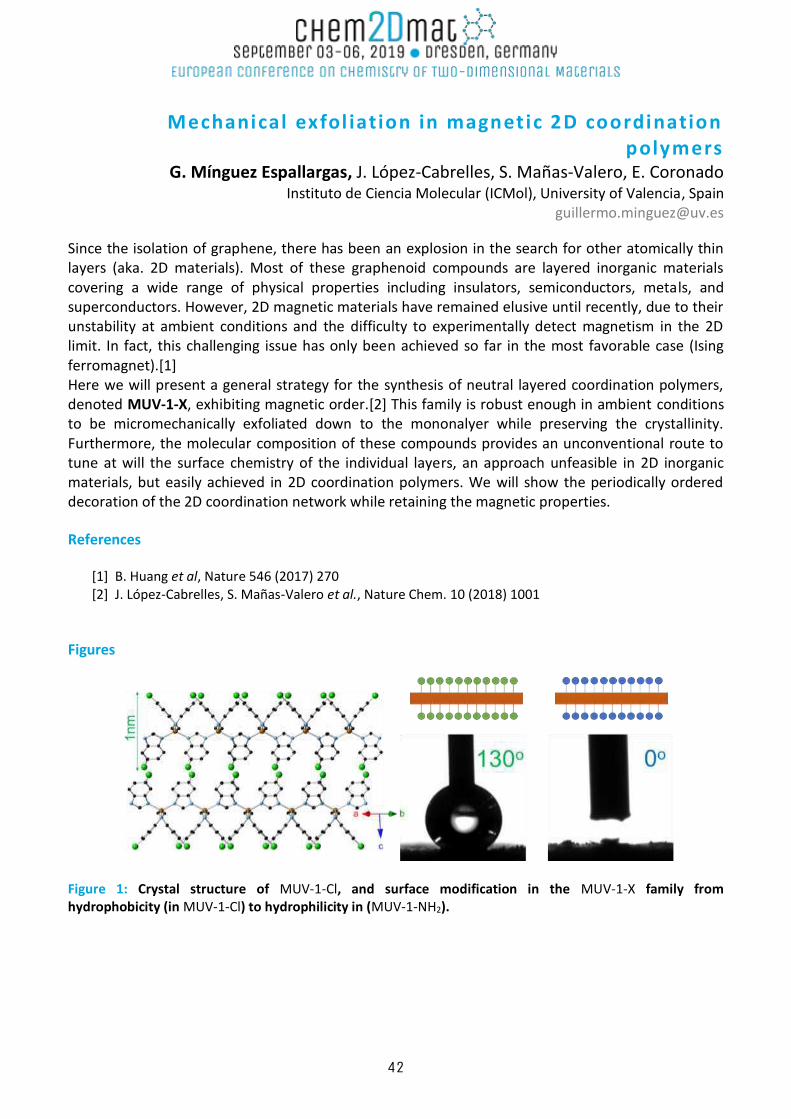
Mechanical exfol iation in magnet ic 2D coordination polymers
G. Mínguez Espallargas, J. López-Cabrelles, S. Mañas-Valero, E. Coronado Instituto de Ciencia Molecular (ICMol), University of Valencia, Spain
Since the isolation of graphene, there has been an explosion in the search for other atomically thin layers (aka. 2D materials). Most of these graphenoid compounds are layered inorganic materials covering a wide range of physical properties including insulators, semiconductors, metals, and superconductors. However, 2D magnetic materials have remained elusive until recently, due to their unstability at ambient conditions and the difficulty to experimentally detect magnetism in the 2D limit. In fact, this challenging issue has only been achieved so far in the most favorable case (Ising ferromagnet).[1] Here we will present a general strategy for the synthesis of neutral layered coordination polymers, denoted MUV-1-X, exhibiting magnetic order.[2] This family is robust enough in ambient conditions to be micromechanically exfoliated down to the mononalyer while preserving the crystallinity. Furthermore, the molecular composition of these compounds provides an unconventional route to tune at will the surface chemistry of the individual layers, an approach unfeasible in 2D inorganic materials, but easily achieved in 2D coordination polymers. We will show the periodically ordered decoration of the 2D coordination network while retaining the magnetic properties. References
[1] B. Huang et al, Nature 546 (2017) 270 [2] J. López-Cabrelles, S. Mañas-Valero et al., Nature Chem. 10 (2018) 1001
Figures
Figure 1: Crystal structure of MUV-1-Cl, and surface modification in the MUV-1-X family from hydrophobicity (in MUV-1-Cl) to hydrophilicity in (MUV-1-NH2).
42
On-surface synthesis of nanostructure d graphene: from 0D to 2D
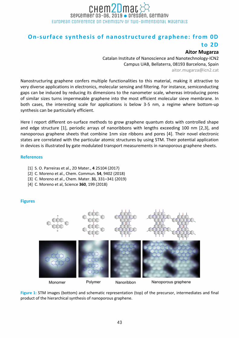
Aitor Mugarza Catalan Institute of Nanoscience and Nanotechnology-ICN2
Campus UAB, Bellaterra, 08193 Barcelona, Spain [email protected]
Nanostructuring graphene confers multiple functionalities to this material, making it attractive to very diverse applications in electronics, molecular sensing and filtering. For instance, semiconducting gaps can be induced by reducing its dimensions to the nanometer scale, whereas introducing pores of similar sizes turns impermeable graphene into the most efficient molecular sieve membrane. In both cases, the interesting scale for applications is below 3-5 nm, a regime where bottom-up synthesis can be particularly efficient. Here I report different on-surface methods to grow graphene quantum dots with controlled shape and edge structure [1], periodic arrays of nanoribbons with lengths exceeding 100 nm [2,3], and nanoporous graphene sheets that combine 1nm size ribbons and pores [4]. Their novel electronic states are correlated with the particular atomic structures by using STM. Their potential application in devices is illustrated by gate modulated transport measurements in nanoporous graphene sheets.
References
[1] S. O. Parreiras et al., 2D Mater., 4 25104 (2017) [2] C. Moreno et al., Chem. Commun. 54, 9402 (2018) [3] C. Moreno et al., Chem. Mater. 31, 331–341 (2019) [4] C. Moreno et al, Science 360, 199 (2018)
Figures
Figure 1: STM images (bottom) and schematic representation (top) of the precursor, intermediates and final product of the hierarchical synthesis of nanoporous graphene.
43
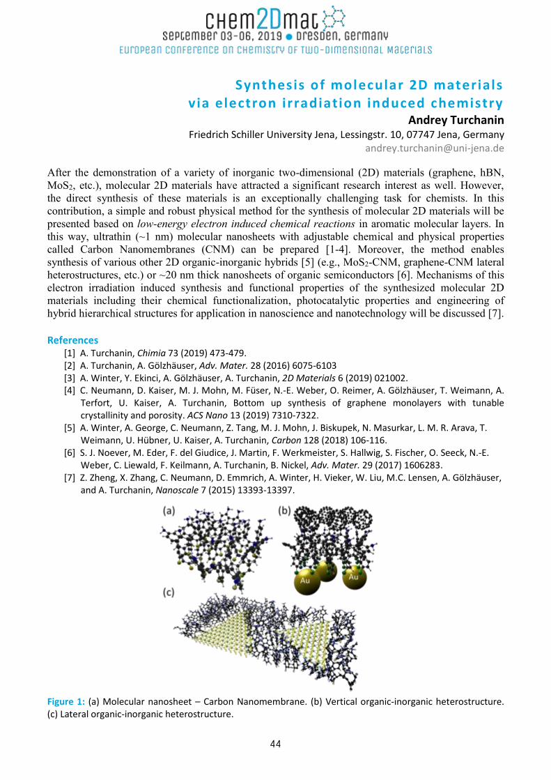
Synthesis of molecular 2D materials v ia electron i rradiation induced chemistry
Andrey Turchanin Friedrich Schiller University Jena, Lessingstr. 10, 07747 Jena, Germany
After the demonstration of a variety of inorganic two-dimensional (2D) materials (graphene, hBN,
MoS2, etc.), molecular 2D materials have attracted a significant research interest as well. However,
the direct synthesis of these materials is an exceptionally challenging task for chemists. In this
contribution, a simple and robust physical method for the synthesis of molecular 2D materials will be
presented based on low-energy electron induced chemical reactions in aromatic molecular layers. In
this way, ultrathin (~1 nm) molecular nanosheets with adjustable chemical and physical properties
called Carbon Nanomembranes (CNM) can be prepared [1-4]. Moreover, the method enables
synthesis of various other 2D organic-inorganic hybrids [5] (e.g., MoS2-CNM, graphene-CNM lateral
heterostructures, etc.) or ~20 nm thick nanosheets of organic semiconductors [6]. Mechanisms of this
electron irradiation induced synthesis and functional properties of the synthesized molecular 2D
materials including their chemical functionalization, photocatalytic properties and engineering of
hybrid hierarchical structures for application in nanoscience and nanotechnology will be discussed [7]. References
[1] A. Turchanin, Chimia 73 (2019) 473-479. [2] A. Turchanin, A. Gölzhäuser, Adv. Mater. 28 (2016) 6075-6103 [3] A. Winter, Y. Ekinci, A. Gölzhäuser, A. Turchanin, 2D Materials 6 (2019) 021002. [4] C. Neumann, D. Kaiser, M. J. Mohn, M. Füser, N.-E. Weber, O. Reimer, A. Gölzhäuser, T. Weimann, A.
Terfort, U. Kaiser, A. Turchanin, Bottom up synthesis of graphene monolayers with tunable crystallinity and porosity. ACS Nano 13 (2019) 7310-7322.
[5] A. Winter, A. George, C. Neumann, Z. Tang, M. J. Mohn, J. Biskupek, N. Masurkar, L. M. R. Arava, T. Weimann, U. Hübner, U. Kaiser, A. Turchanin, Carbon 128 (2018) 106-116.
[6] S. J. Noever, M. Eder, F. del Giudice, J. Martin, F. Werkmeister, S. Hallwig, S. Fischer, O. Seeck, N.-E. Weber, C. Liewald, F. Keilmann, A. Turchanin, B. Nickel, Adv. Mater. 29 (2017) 1606283.
[7] Z. Zheng, X. Zhang, C. Neumann, D. Emmrich, A. Winter, H. Vieker, W. Liu, M.C. Lensen, A. Gölzhäuser, and A. Turchanin, Nanoscale 7 (2015) 13393-13397.
Figure 1: (a) Molecular nanosheet – Carbon Nanomembrane. (b) Vertical organic-inorganic heterostructure. (c) Lateral organic-inorganic heterostructure.
44
Grapheneoxidebasedmateria ls for e lectrochemical (bio)sensing
ChiaraZanardi DepartmentofChemicalandGeologicalSciences,UniversitàdiModenaeReggioEmilia,
viaG.Campi103,41125Modena,ItalyInstituteofOrganicSynthesisandPhotoreactivity,NationalResearchCouncil
viaP.Gobetti101-40129Bologna,Italy,[email protected]
Non-invasive sensors, which accuratelymeasure biomarkers in biological fluids, allow for amorepersonalized approach to fitness goals and to healthmonitoring. They define the levels ofmanychemical parameters through portable devices, which can be used far from equipped laboratorycenters and by untrained personnel. The opportunity to develop even wearable sensors, withwireless connectivity, represents the next generation of integrated lab-on-chip technology. In thistalkwewilldiscuss theadvantagesofusinggrapheneoxide (GO)as the sensingelementof thesedetectionsystems. Inparticular,thetalkwilltakeintoaccountthedevelopmentofsensorsforthedetectionoflactateandglucose,whicharebiomarkersofaphysicalexercise,andforthedetectionofdrugsofabuseinurinesamples[1].
Thephysico-chemicalpropertiesofbothpristineandchemicallyfunctionalizedGOinthedetectionofthetargetanalytewerestudiedcombiningtheresultscomingfromelectrochemical,spectroscopicandmorphologicmeasurements[2].Thisapproachallowedustoobtainuseful informationforthefurtherimprovementoftheanalyticalperformancesofthedevices.
References
[1] G.Maccaferri,F.Terzi,Z.Xia,F.Vulcano,A.Liscio,V.Palermo,C.Zanardi,Sens.Act.B,281(2019)739.[2] G.Maccaferri,C.Zanardi,Z.Xia,A.Kovtun,A.Liscio,F.Terzi,V.Palermo,R.Seeber,Carbon120(2017)
165.
45

INVITED SPEAKERS (Industrial Forum)
High-yield production and characterization of graphene -
based chemiresistors for environmental sensing
Jorge Adatti, Caterina Travan, Dr. Ulrich Krumbein Infineon Technologies AG, 81726 Munich, Germany
With the growing awareness towards the necessity of protecting the environment, the demand on techniques for real-time detecting and monitoring different hazardous gases has increased notably. In this regard, solid-state gas sensors, due to their small sizes, high sensitivities towards a wide range of gases, and their low cost, offer advantages over other techniques and are therefore regarded as the best candidates for the development of commercial gas sensors [1]. Among different options, graphene-based materials – especially under the architectural configuration of a chemiresistor, i.e. where the gas adsorption is quantified through a measurement of resistance variation – have aroused great interest due to their atom-thick, 2D-nature and its diverse striking properties. A large area to volume ratio, detectable single-atom interaction with gas adsorbates, tunability of sensitivity via functionalization, as well as low-cost and high-scale fabrication by chemical methods constitute some of the most noteworthy advantages of the use of graphene for environmental sensing [2]. In this sense, a crucial aspect in the fulfillment of a high-yield production is the material deposition technique. Here, inkjet printing has proven promising since it enables the large area fabrication of different components on different substrates by a simple, controlled, high-scalable, and versatile process [3]. By means of inkjet printing liquid phase materials mostly consisting of a dissolved solute are deposited onto a substrate. The printing process comprises the droplet ejection from the ink supply through a nozzle, the deposition and spreading of the ink on the substrate, as well as its drying in order to ultimately produce a solid deposit [4]. In spite of all the advantages, inkjet printing of graphene-based inks goes along with multiple difficulties which need to be addressed, being the ink selection and its performance the most relevant one. Furthermore, due to the device’s solely resistive nature, the extraction of as much information as possible out of relatively simple resistance measurements is vital. In the current presentation, we will give an overview of inkjet-printed graphene-based chemiresistors at Infineon and also provide an insight in the characterization of the printing process as well as the ink performance. References
[1] S. Capone, A. Forleo, L. Francioso, R. Rella, P. Siciliano, J. Spadavecchia, D. Presicce,and A. Taurino, “Solid state gas sensors: state of the art and future activities,” Journal of Optoelectronics and Advanced Materials 5, 1335–1348 (2003).
[2] W. Yuan and G. Shi, “Graphene-based gas sensors,” Journal of Materials Chemistry A1, 10078–10091 (2013).
[3] F. Torrisi, T. Hasan, W. Wu, Z. Sun, A. Lombardo, T. S. Kulmala, G.-W. Hsieh, S. Jung, F. Bonaccorso, P. J. Paul et al., “Inkjet-printed graphene electronics,” ACS nano 6, 2992–3006 (2012).
[4] M. Singh, H. M. Haverinen, P. Dhagat, and G. E. Jabbour, “Inkjet printing—process and its applications,” Advanced materials 22, 673–685 (2010).
47
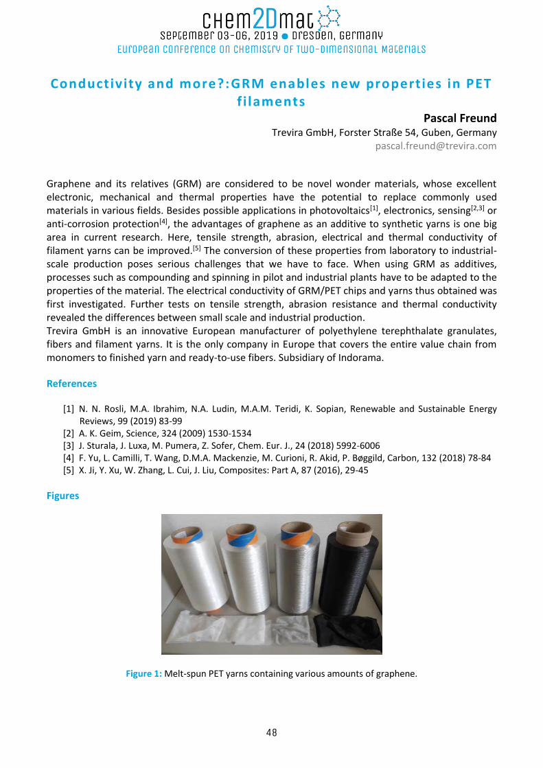
Conductivity and more?: GRM enables new propert ies in PET f i laments
Pascal Freund Trevira GmbH, Forster Straße 54, Guben, Germany
Graphene and its relatives (GRM) are considered to be novel wonder materials, whose excellent electronic, mechanical and thermal properties have the potential to replace commonly used materials in various fields. Besides possible applications in photovoltaics[1], electronics, sensing[2,3] or anti-corrosion protection[4], the advantages of graphene as an additive to synthetic yarns is one big area in current research. Here, tensile strength, abrasion, electrical and thermal conductivity of filament yarns can be improved.[5] The conversion of these properties from laboratory to industrial-scale production poses serious challenges that we have to face. When using GRM as additives, processes such as compounding and spinning in pilot and industrial plants have to be adapted to the properties of the material. The electrical conductivity of GRM/PET chips and yarns thus obtained was first investigated. Further tests on tensile strength, abrasion resistance and thermal conductivity revealed the differences between small scale and industrial production. Trevira GmbH is an innovative European manufacturer of polyethylene terephthalate granulates, fibers and filament yarns. It is the only company in Europe that covers the entire value chain from monomers to finished yarn and ready-to-use fibers. Subsidiary of Indorama. References
[1] N. N. Rosli, M.A. Ibrahim, N.A. Ludin, M.A.M. Teridi, K. Sopian, Renewable and Sustainable Energy Reviews, 99 (2019) 83-99
[2] A. K. Geim, Science, 324 (2009) 1530-1534 [3] J. Sturala, J. Luxa, M. Pumera, Z. Sofer, Chem. Eur. J., 24 (2018) 5992-6006 [4] F. Yu, L. Camilli, T. Wang, D.M.A. Mackenzie, M. Curioni, R. Akid, P. Bøggild, Carbon, 132 (2018) 78-84 [5] X. Ji, Y. Xu, W. Zhang, L. Cui, J. Liu, Composites: Part A, 87 (2016), 29-45
Figures
Figure 1: Melt-spun PET yarns containing various amounts of graphene.
48
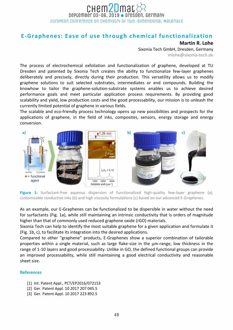
E-Graphenes: Ease of use through chemical functionalization Martin R. Lohe
Sixonia Tech GmbH, Dresden, Germany [email protected]
The process of electrochemical exfoliation and functionalization of graphene, developed at TU Dresden and patented by Sixonia Tech creates the ability to functionalize few-layer graphenes deliberately and precisely, directly during their production. This versatility allows us to modify graphene solutions to suit selected substrates, intermediates or end compounds. Building the knowhow to tailor the graphene-solution-substrate systems enables us to achieve desired performance goals and meet particular application process requirements. By providing good scalability and yield, low production costs and the good processability, our mission is to unleash the currently limited potential of graphene in various fields. The scalable and eco-friendly process technology opens up new possibilities and prospects for the applications of graphene, in the field of inks, composites, sensors, energy storage and energy conversion.
Figure 1: Surfactant-free aqueous dispersion of functionalized high-quality few-layer graphene (a), customizable conductive inks (b) and high viscosity formulations (c) based on our advanced E-Graphenes.
As an example, our E-Graphenes can be functionalized to be dispersible in water without the need for surfactants (Fig. 1a), while still maintaining an intrinsic conductivity that is orders of magnitude higher than that of commonly used reduced graphene oxide (rGO) materials. Sixonia Tech can help to identify the most suitable graphene for a given application and formulate it (Fig. 1b, c), to facilitate its integration into the desired applications. Compared to other “graphene” products, E-Graphenes show a superior combination of tailorable properties within a single material, such as large flake-size in the µm-range, low thickness in the range of 1-10 layers and good processability. Unlike in GO, the defined functional groups can provide an improved processability, while still maintaining a good electrical conductivity and reasonable sheet size. References
[1] Int. Patent Appl., PCT/EP2016/072153 [2] Ger. Patent Appl. 10 2017 207 045.5 [3] Ger. Patent Appl. 10 2017 223 892.5
a) b) c)
49
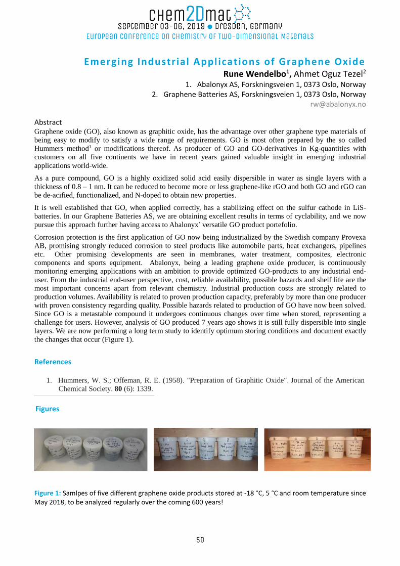
Emerging Industr ial Appl ications of Graphene Oxide Rune Wendelbo1, Ahmet Oguz Tezel2
1. Abalonyx AS, Forskningsveien 1, 0373 Oslo, Norway 2. Graphene Batteries AS, Forskningsveien 1, 0373 Oslo, Norway
Abstract Graphene oxide (GO), also known as graphitic oxide, has the advantage over other graphene type materials of
being easy to modify to satisfy a wide range of requirements. GO is most often prepared by the so called
Hummers method1 or modifications thereof. As producer of GO and GO-derivatives in Kg-quantities with
customers on all five continents we have in recent years gained valuable insight in emerging industrial
applications world-wide.
As a pure compound, GO is a highly oxidized solid acid easily dispersible in water as single layers with a
thickness of 0.8 – 1 nm. It can be reduced to become more or less graphene-like rGO and both GO and rGO can
be de-acified, functionalized, and N-doped to obtain new properties.
It is well established that GO, when applied correctly, has a stabilizing effect on the sulfur cathode in LiS-
batteries. In our Graphene Batteries AS, we are obtaining excellent results in terms of cyclability, and we now
pursue this approach further having access to Abalonyx’ versatile GO product portefolio.
Corrosion protection is the first application of GO now being industrialized by the Swedish company Provexa
AB, promising strongly reduced corrosion to steel products like automobile parts, heat exchangers, pipelines
etc. Other promising developments are seen in membranes, water treatment, composites, electronic
components and sports equipment. Abalonyx, being a leading graphene oxide producer, is continuously
monitoring emerging applications with an ambition to provide optimized GO-products to any industrial end-
user. From the industrial end-user perspective, cost, reliable availability, possible hazards and shelf life are the
most important concerns apart from relevant chemistry. Industrial production costs are strongly related to
production volumes. Availability is related to proven production capacity, preferably by more than one producer
with proven consistency regarding quality. Possible hazards related to production of GO have now been solved.
Since GO is a metastable compound it undergoes continuous changes over time when stored, representing a
challenge for users. However, analysis of GO produced 7 years ago shows it is still fully dispersible into single
layers. We are now performing a long term study to identify optimum storing conditions and document exactly
the changes that occur (Figure 1).
References
1. Hummers, W. S.; Offeman, R. E. (1958). "Preparation of Graphitic Oxide". Journal of the American
Chemical Society. 80 (6): 1339.
Figure 1: Samlpes of five different graphene oxide products stored at -18 °C, 5 °C and room temperature since May 2018, to be analyzed regularly over the coming 600 years!
Figures
50

ORAL CONTRIBUTIONS
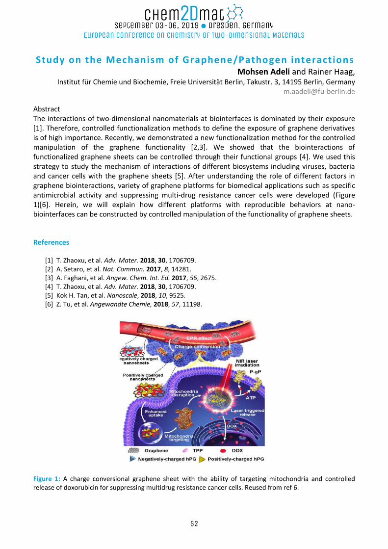
Study on the Mechanism of Graphene/Pathogen interactions Mohsen Adeli and Rainer Haag,
Institut für Chemie und Biochemie, Freie Universität Berlin, Takustr. 3, 14195 Berlin, Germany
Abstract The interactions of two-dimensional nanomaterials at biointerfaces is dominated by their exposure [1]. Therefore, controlled functionalization methods to define the exposure of graphene derivatives is of high importance. Recently, we demonstrated a new functionalization method for the controlled manipulation of the graphene functionality [2,3]. We showed that the biointeractions of functionalized graphene sheets can be controlled through their functional groups [4]. We used this strategy to study the mechanism of interactions of different biosystems including viruses, bacteria and cancer cells with the graphene sheets [5]. After understanding the role of different factors in graphene biointeractions, variety of graphene platforms for biomedical applications such as specific antimicrobial activity and suppressing multi-drug resistance cancer cells were developed (Figure 1)[6]. Herein, we will explain how different platforms with reproducible behaviors at nano-biointerfaces can be constructed by controlled manipulation of the functionality of graphene sheets. References
[1] T. Zhaoxu, et al. Adv. Mater. 2018, 30, 1706709. [2] A. Setaro, et al. Nat. Commun. 2017, 8, 14281. [3] A. Faghani, et al. Angew. Chem. Int. Ed. 2017, 56, 2675. [4] T. Zhaoxu, et al. Adv. Mater. 2018, 30, 1706709. [5] Kok H. Tan, et al. Nanoscale, 2018, 10, 9525. [6] Z. Tu, et al. Angewandte Chemie, 2018, 57, 11198.
Figure 1: A charge conversional graphene sheet with the ability of targeting mitochondria and controlled release of doxorubicin for suppressing multidrug resistance cancer cells. Reused from ref 6.
52
Effect of Graphene on the Crystal l isat ion of Glycine Adriana Alieva1, Matthew Boyes1, Jincheng Tong1, Vaiva Nagyte1, Manuel Melle3,
Thomas Vetter2, Cinzia Casiraghi1
1 School of Chemistry, University of Manchester, UK 2 School of Chemical Engineering and Analytical Science, University of Manchester, UK
3 CICECO, University of Aveiro, Portugal
Nucleation, the initial stage of molecular self-assembly in crystallisation, is still not fully understood.
Thus, producing crystals of the desired form (polymorph) is a current challenge faced by the industry
and academia1. Templated crystallisation, where nucleation can be initiated at specific sites of the
substrate or by impurities, is a promising approach to achieve preferential nucleation. Graphene has
never been utilized to template the crystallistion of organic molecules so far, despite its attractive
properties2, which include tunability of its surface via covalent functionalisation and ease of solution
processability.
This work investigates the use of graphene on the crystallisation of the simplest amino acid, glycine.
The polymorphism of glycine is investigated by Raman spectroscopy as this technique is able to
detect even a small trace of different polymorphs, well below the sensitivity of X-Ray Diffraction
(XRD). Our results show that graphene does affect the polymorphic outcome of glycine, but this
strongly depends on the surface properties of graphene, in agreement with the computational
studies3.
References
[1] B. Moulton, M. J. Zaworotko, Chemical Reviews, 101(2001), pp. 1629– 1658. [2] A. Geim, Science, 5934(2009), pp. 1530–1534. [3] M. Boyes, A. Alieva, J. Tong, V. Nagyte, M. Melle, T. Vetter, C. Casiraghi – to be submitted.
53
Towards optimized preparation of few -layer antimonene and unveil ing its oxidation tendency
Mhamed Assebban,1,2 Carlos Gibaja,3 Michael Fickert,2 Iñigo Torres,3 Erik Weinreich,2 Stefan Wolff,4 Roland Gillen,4 Janina Maultzsch,4 Maria Varela,5 Sherman Tan Jun
Rong, 6 Kian Ping Loh,6 Enrique García Michel,7,8 Félix Zamora,3,8 and Gonzalo Abellán,1,2
1 Instituto de Ciencia Molecular (ICMol), Universidad de Valencia, Catedrático José Beltrán 2, Paterna, Valencia, Spain.2 Joint Institute of Advanced Materials and Processes (ZMP), Friedrich-
Alexander-Universität Erlangen-Nürnberg (FAU), Dr.-Mack-Straße 81, Fürth, Germany.3 Departamento de Química Inorgánica, Universidad Autónoma de Madrid, Spain.4 Department of Physics, Friedrich-Alexander University Erlangen-Nürnberg, Staudtstrasse 7, Erlangen, Germany.5
Departamento de Física de Materiales, Universidad Complutense de Madrid, Instituto Pluridisciplinar, Instituto de Magnetismo Aplicado, Madrid, Spain.6 Department of Chemistry National University of Singapore 3 Science Drive 3, Singapore.7 Departamento de Física de la
Materia Condensada Universidad Autónoma de Madrid, Spain.8 Condensed Matter Physics Center (IFIMAC) Universidad Autónoma de Madrid, Spain.
Abstract Antimonene, a monolayer of β-antimony, has recently become the focus of intense research owing to its intriguing semiconducting properties, good electronic mobility and chemical reactivity, which makes it highly desirable for applications in (opto)electronics, energy storage, and organic catalysis, to name a few[1]. Beyond other 2D materials, antimonene is of particular interest because of its high thermodynamic stability under ambient conditions as well as its predicted 2D topological feature stemming from its intrinsic spin–orbit coupling property[2]. However, the absence of a reliable method for the preparation of high-quality antimonene in large quantities hinders the development of antimonene-based devices despite the tremendous efforts devoted for this end[3]. Here, we present a systematic optimization of the preparation of Few-layer antimonene (FLA) through top-down methods, namely liquid-phase exfoliation and mechanical delamination, while simultaneously deciphering its structural and morphological characteristics using a set of upfront characterization techniques. Moreover, and whilst the surface chemistry of several 2D-materials and their oxygen-sensitivity have been fully addressed[4], the oxidation behavior of antimonene remains poorly investigated. In this regard, we conducted an insightful investigation of the oxidation behavior of FLA and complemented the obtained results with DFT calculations. This work pushes forward the controlled synthesis of FLA via simple and facile methods and yields valuable information on its oxidation tendency, thus paving the way towards its potential application in various technologies. References [1] V. Lloret, M.Á. Rivero-Crespo, J.A. Vidal-Moya, S. Wild, A. Doménech-Carbó, B.S.J. Heller, S. Shin, H.-P.
Steinrück, F. Maier, F. Hauke, M. Varela, A. Hirsch, A. Leyva-Pérez, G. Abellán, Nature Communications 10 (2019).
[2] M. Zhao, X. Zhang, L. Li, Scientific Reports 5 (2015) 16108. [3] C. Gibaja, D. Rodriguez‐San‐Miguel, P. Ares, J. Gómez‐Herrero, M. Varela, R. Gillen, J. Maultzsch, F. Hauke,
A. Hirsch, G. Abellán, F. Zamora, Angewandte Chemie International Edition 55 (2016) 14345–14349. [4] G. Abellán, S. Wild, V. Lloret, N. Scheuschner, R. Gillen, U. Mundloch, J. Maultzsch, M. Varela, F. Hauke, A.
Hirsch, J. Am. Chem. Soc. 139 (2017) 10432–10440.
54
The unique interplay between interfacia l chemistry and electronic structure in graphene
Kannan Balasubramanian, Michel Wehrhold, Tilmann J Neubert, Anur Yadav, Tobias Grosser, Nur Selin Kaya, Emil Fuhry
Humboldt Universität zu Berlin, 10099 Berlin, Germany nano.anchem~at~hu-berlin.de
Abstract For many envisioned applications using graphene, such as sensors, fuel cells and electrocatalysts, it is of utmost importance to have a detailed understanding of various physicochemical aspects of the interface of graphene with its immediate environment. [1] This need arises due to the unique material properties of graphene: electron transport in graphene is purely two-dimensional, the electronic density at graphene is much lower in comparison to metal electrodes, and electron transfer across the interface is expected to have a strong effect on the graphene electronic structure itself. Moreover, functional groups and metallic structures on and around graphene (either present or introduced deliberately) will affect the electronic structure and the chemistry of graphene. [2] In this talk, we present basic examples of how the interfacial properties dictate the behavior of graphene in a liquid environment. Specifically, we demonstrate how electrostatic effects at the graphene interface [3] modulate the kinetics of electron transfer, and how electron transfer in turn affects the electronic properties of graphene. Moreover, the presence of functional groups and metal structures even in trace amounts [4] either at the basal plane or exclusively at the edge [5] is found to have a significant effect on the electron transfer characteristics. References
[1] L. Zuccaro, J. Krieg, A: Desideri, K. Kern, K. Balasubramanian, Sci. Rep. 5 (2015), 11794. [2] J. Hui, S. Pakhira, R. Bhargava, Z.J. Barton, X. Zhou, A.J. Chinderli, J.L. Mendoza-Cortes, J. Rodriguez-
Lopez., ACS Nano 12 (2018), 2980. [3] N.S. Kaya, A. Yadav, M. Wehrhold, L. Zuccaro, K. Balasubramanian, ACS Omega 3 (2018), 7133. [4] R.M. Iost, F. Crespilho, L. Zukkaro, H.K. Yu, A.M. Wodtke, K. Kern, K. Balasubramanian,
ChemElectroChem 1 (2014), 2070. [5] A. Yadav, R.M. Iost, T.J. Neubert, S. Baylan, T. Schmid, K. Balasubramanian, Chem. Sci. 10 (2019), 936.
55
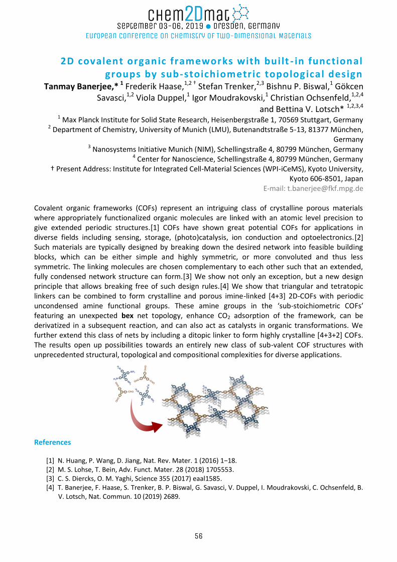
2D covalent organic frameworks with bui lt - in functional groups by sub-stoichiometric topolog ical design
Tanmay Banerjee,* 1 Frederik Haase,1,2 † Stefan Trenker,2,3 Bishnu P. Biswal,1 Gökcen Savasci,1,2 Viola Duppel,1 Igor Moudrakovski,1 Christian Ochsenfeld,1,2,4
and Bettina V. Lotsch* 1,2,3,4 1 Max Planck Institute for Solid State Research, Heisenbergstraße 1, 70569 Stuttgart, Germany
2 Department of Chemistry, University of Munich (LMU), Butenandtstraße 5-13, 81377 München, Germany
3 Nanosystems Initiative Munich (NIM), Schellingstraße 4, 80799 München, Germany 4 Center for Nanoscience, Schellingstraße 4, 80799 München, Germany
† Present Address: Institute for Integrated Cell-Material Sciences (WPI-iCeMS), Kyoto University, Kyoto 606-8501, Japan
E-mail: [email protected]
Covalent organic frameworks (COFs) represent an intriguing class of crystalline porous materials where appropriately functionalized organic molecules are linked with an atomic level precision to give extended periodic structures.[1] COFs have shown great potential COFs for applications in diverse fields including sensing, storage, (photo)catalysis, ion conduction and optoelectronics.[2] Such materials are typically designed by breaking down the desired network into feasible building blocks, which can be either simple and highly symmetric, or more convoluted and thus less symmetric. The linking molecules are chosen complementary to each other such that an extended, fully condensed network structure can form.[3] We show not only an exception, but a new design principle that allows breaking free of such design rules.[4] We show that triangular and tetratopic linkers can be combined to form crystalline and porous imine-linked [4+3] 2D-COFs with periodic uncondensed amine functional groups. These amine groups in the ‘sub-stoichiometric COFs’ featuring an unexpected bex net topology, enhance CO2 adsorption of the framework, can be derivatized in a subsequent reaction, and can also act as catalysts in organic transformations. We further extend this class of nets by including a ditopic linker to form highly crystalline [4+3+2] COFs. The results open up possibilities towards an entirely new class of sub-valent COF structures with unprecedented structural, topological and compositional complexities for diverse applications.
References
[1] N. Huang, P. Wang, D. Jiang, Nat. Rev. Mater. 1 (2016) 1−18. [2] M. S. Lohse, T. Bein, Adv. Funct. Mater. 28 (2018) 1705553. [3] C. S. Diercks, O. M. Yaghi, Science 355 (2017) eaal1585. [4] T. Banerjee, F. Haase, S. Trenker, B. P. Biswal, G. Savasci, V. Duppel, I. Moudrakovski, C. Ochsenfeld, B.
V. Lotsch, Nat. Commun. 10 (2019) 2689.
56
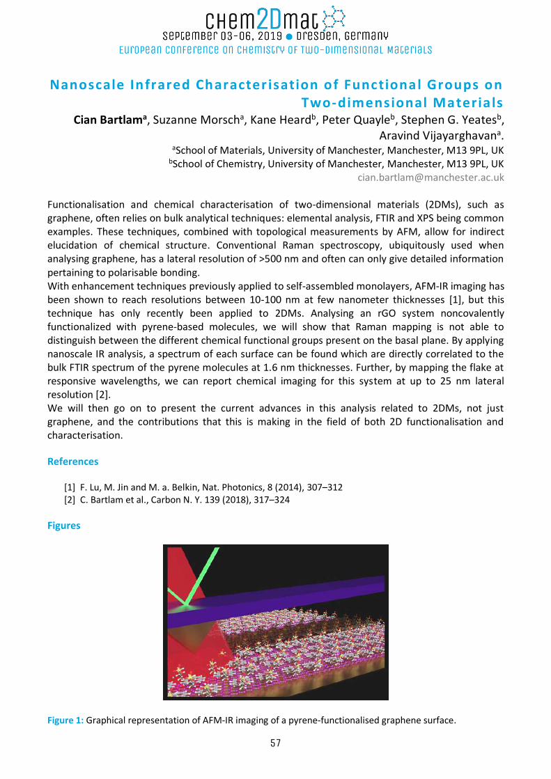
Nanoscale Infrared Character isation of Functional Groups on Two-dimensional Materia ls
Cian Bartlama, Suzanne Morscha, Kane Heardb, Peter Quayleb, Stephen G. Yeatesb, Aravind Vijayarghavana.
aSchool of Materials, University of Manchester, Manchester, M13 9PL, UK bSchool of Chemistry, University of Manchester, Manchester, M13 9PL, UK
Functionalisation and chemical characterisation of two-dimensional materials (2DMs), such as graphene, often relies on bulk analytical techniques: elemental analysis, FTIR and XPS being common examples. These techniques, combined with topological measurements by AFM, allow for indirect elucidation of chemical structure. Conventional Raman spectroscopy, ubiquitously used when analysing graphene, has a lateral resolution of >500 nm and often can only give detailed information pertaining to polarisable bonding. With enhancement techniques previously applied to self-assembled monolayers, AFM-IR imaging has been shown to reach resolutions between 10-100 nm at few nanometer thicknesses [1], but this technique has only recently been applied to 2DMs. Analysing an rGO system noncovalently functionalized with pyrene-based molecules, we will show that Raman mapping is not able to distinguish between the different chemical functional groups present on the basal plane. By applying nanoscale IR analysis, a spectrum of each surface can be found which are directly correlated to the bulk FTIR spectrum of the pyrene molecules at 1.6 nm thicknesses. Further, by mapping the flake at responsive wavelengths, we can report chemical imaging for this system at up to 25 nm lateral resolution [2]. We will then go on to present the current advances in this analysis related to 2DMs, not just graphene, and the contributions that this is making in the field of both 2D functionalisation and characterisation.
References
[1] F. Lu, M. Jin and M. a. Belkin, Nat. Photonics, 8 (2014), 307–312 [2] C. Bartlam et al., Carbon N. Y. 139 (2018), 317–324
Figures
Figure 1: Graphical representation of AFM-IR imaging of a pyrene-functionalised graphene surface.
57
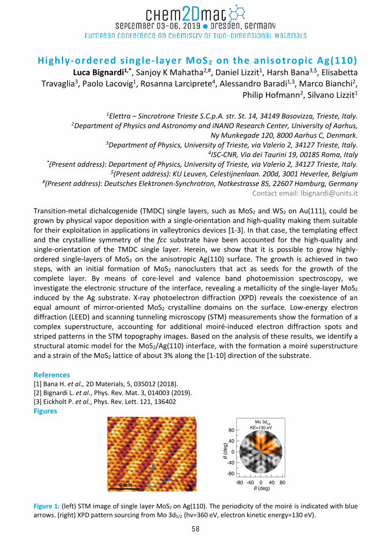
Highly-ordered sing le- layer MoS 2 on the anisotropic Ag(110) Luca Bignardi1,*, Sanjoy K Mahatha2,#, Daniel Lizzit1, Harsh Bana3,$, Elisabetta
Travaglia3, Paolo Lacovig1, Rosanna Larciprete4, Alessandro Baradi1,3, Marco Bianchi2, Philip Hofmann2, Silvano Lizzit1
1Elettra – Sincrotrone Trieste S.C.p.A. str. St. 14, 34149 Basovizza, Trieste, Italy.
2Department of Physics and Astronomy and iNANO Research Center, University of Aarhus, Ny Munkegade 120, 8000 Aarhus C, Denmark.
3Department of Physics, University of Trieste, via Valerio 2, 34127 Trieste, Italy. 4ISC-CNR, Via dei Taurini 19, 00185 Roma, Italy
*(Present address): Department of Physics, University of Trieste, via Valerio 2, 34127 Trieste, Italy. $(Present address): KU Leuven, Celestijnenlaan. 200d, 3001 Heverlee, Belgium
#(Present address): Deutsches Elektronen-Synchrotron, Notkestrasse 85, 22607 Hamburg, Germany Contact email: [email protected]
Transition-metal dichalcogenide (TMDC) single layers, such as MoS2 and WS2 on Au(111), could be grown by physical vapor deposition with a single-orientation and high-quality making them suitable for their exploitation in applications in valleytronics devices [1-3]. In that case, the templating effect and the crystalline symmetry of the fcc substrate have been accounted for the high-quality and single-orientation of the TMDC single layer. Herein, we show that it is possible to grow highly-ordered single-layers of MoS2 on the anisotropic Ag(110) surface. The growth is achieved in two steps, with an initial formation of MoS2 nanoclusters that act as seeds for the growth of the complete layer. By means of core-level and valence band photoemission spectroscopy, we investigate the electronic structure of the interface, revealing a metallicity of the single-layer MoS2 induced by the Ag substrate. X-ray photoelectron diffraction (XPD) reveals the coexistence of an equal amount of mirror-oriented MoS2 crystalline domains on the surface. Low-energy electron diffraction (LEED) and scanning tunneling microscopy (STM) measurements show the formation of a complex superstructure, accounting for additional moiré-induced electron diffraction spots and striped patterns in the STM topography images. Based on the analysis of these results, we identify a structural atomic model for the MoS2/Ag(110) interface, with the formation a moiré superstructure and a strain of the MoS2 lattice of about 3% along the [1-10] direction of the substrate. References [1] Bana H. et al., 2D Materials, 5, 035012 (2018). [2] Bignardi L. et al., Phys. Rev. Mat. 3, 014003 (2019). [3] Eickholt P. et al., Phys. Rev. Lett. 121, 136402 Figures
Figure 1: (left) STM image of single layer MoS2 on Ag(110). The periodicity of the moiré is indicated with blue arrows. (right) XPD pattern sourcing from Mo 3d5/2 (hv=360 eV, electron kinetic energy=130 eV).
-80
-40
0
40
80
-80 -40 0 40 80
Mo 3d5/2KE=130 eV
θ (deg)
θ (d
eg)
58
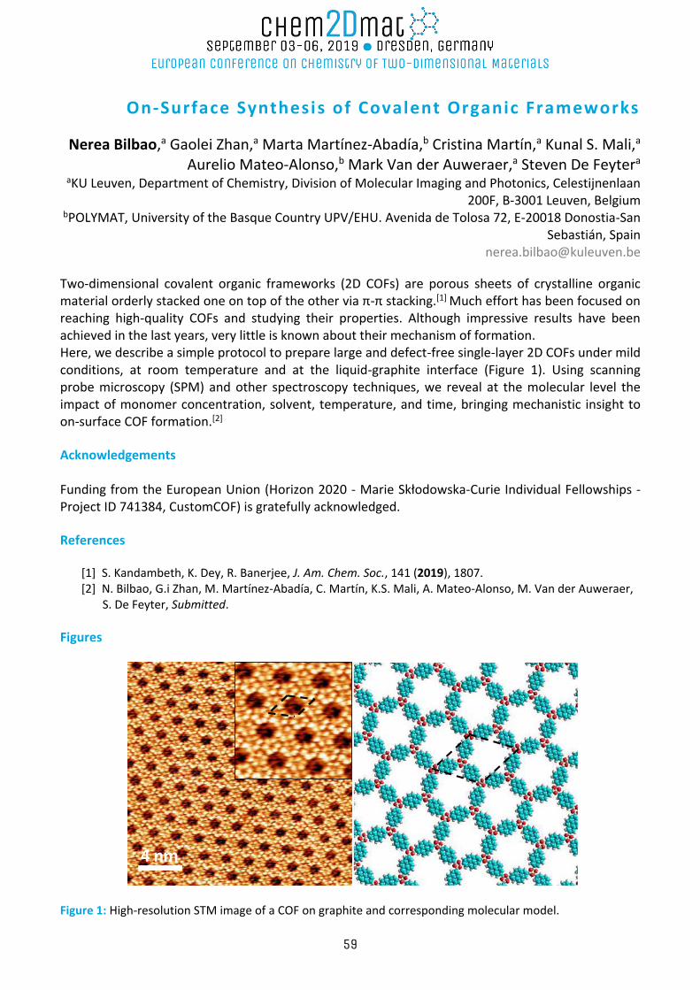
On-Surface Synthesis of Covalent Organic Frameworks
Nerea Bilbao,a Gaolei Zhan,a Marta Martínez-Abadía,b Cristina Martín,a Kunal S. Mali,a Aurelio Mateo-Alonso,b Mark Van der Auweraer,a Steven De Feytera
aKU Leuven, Department of Chemistry, Division of Molecular Imaging and Photonics, Celestijnenlaan 200F, B-3001 Leuven, Belgium
bPOLYMAT, University of the Basque Country UPV/EHU. Avenida de Tolosa 72, E-20018 Donostia-San Sebastián, Spain
Two-dimensional covalent organic frameworks (2D COFs) are porous sheets of crystalline organic material orderly stacked one on top of the other via π-π stacking.[1] Much effort has been focused on reaching high-quality COFs and studying their properties. Although impressive results have been achieved in the last years, very little is known about their mechanism of formation. Here, we describe a simple protocol to prepare large and defect-free single-layer 2D COFs under mild conditions, at room temperature and at the liquid-graphite interface (Figure 1). Using scanning probe microscopy (SPM) and other spectroscopy techniques, we reveal at the molecular level the impact of monomer concentration, solvent, temperature, and time, bringing mechanistic insight to on-surface COF formation.[2] Acknowledgements Funding from the European Union (Horizon 2020 - Marie Skłodowska-Curie Individual Fellowships - Project ID 741384, CustomCOF) is gratefully acknowledged. References
[1] S. Kandambeth, K. Dey, R. Banerjee, J. Am. Chem. Soc., 141 (2019), 1807. [2] N. Bilbao, G.i Zhan, M. Martínez-Abadía, C. Martín, K.S. Mali, A. Mateo-Alonso, M. Van der Auweraer,
S. De Feyter, Submitted.
Figures
4 nm
Figure 1: High-resolution STM image of a COF on graphite and corresponding molecular model.
59
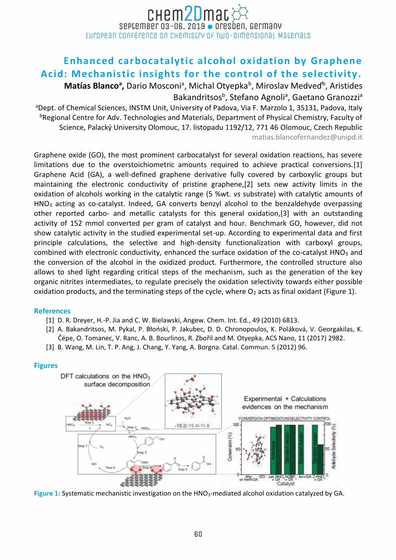
Enhanced carbocatalyt ic alcohol oxidation by Graphene Acid: Mechanistic insights for the control of the selectiv ity.
Matías Blancoa, Dario Mosconia, Michal Otyepkab, Miroslav Medveďb, Aristides Bakandritsosb, Stefano Agnolia, Gaetano Granozzia
aDept. of Chemical Sciences, INSTM Unit, University of Padova, Via F. Marzolo 1, 35131, Padova, Italy bRegional Centre for Adv. Technologies and Materials, Department of Physical Chemistry, Faculty of
Science, Palacký University Olomouc, 17. listopadu 1192/12, 771 46 Olomouc, Czech Republic [email protected]
Graphene oxide (GO), the most prominent carbocatalyst for several oxidation reactions, has severe limitations due to the overstoichiometric amounts required to achieve practical conversions.[1] Graphene Acid (GA), a well-defined graphene derivative fully covered by carboxylic groups but maintaining the electronic conductivity of pristine graphene,[2] sets new activity limits in the oxidation of alcohols working in the catalytic range (5 %wt. vs substrate) with catalytic amounts of HNO3 acting as co-catalyst. Indeed, GA converts benzyl alcohol to the benzaldehyde overpassing other reported carbo- and metallic catalysts for this general oxidation,[3] with an outstanding activity of 152 mmol converted per gram of catalyst and hour. Benchmark GO, however, did not show catalytic activity in the studied experimental set-up. According to experimental data and first principle calculations, the selective and high-density functionalization with carboxyl groups, combined with electronic conductivity, enhanced the surface oxidation of the co-catalyst HNO3 and the conversion of the alcohol in the oxidized product. Furthermore, the controlled structure also allows to shed light regarding critical steps of the mechanism, such as the generation of the key organic nitrites intermediates, to regulate precisely the oxidation selectivity towards either possible oxidation products, and the terminating steps of the cycle, where O2 acts as final oxidant (Figure 1). References
[1] D. R. Dreyer, H.-P. Jia and C. W. Bielawski, Angew. Chem. Int. Ed., 49 (2010) 6813. [2] A. Bakandritsos, M. Pykal, P. Błonski, P. Jakubec, D. D. Chronopoulos, K. Polakova, V. Georgakilas, K.
Cepe, O. Tomanec, V. Ranc, A. B. Bourlinos, R. Zboril and M. Otyepka, ACS Nano, 11 (2017) 2982. [3] B. Wang, M. Lin, T. P. Ang, J. Chang, Y. Yang, A. Borgna. Catal. Commun. 5 (2012) 96.
Figures
Figure 1: Systematic mechanistic investigation on the HNO3-mediated alcohol oxidation catalyzed by GA.
60
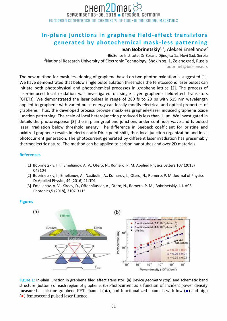
In-plane junctions in graphene f ield-effect transistors generated by photochemical mask -less patterning
Ivan Bobrinetskiy1,2, Aleksei Emelianov2 1BioSense Institute, Dr Zorana Djindjica 1a, Novi Sad, Serbia
2National Research University of Electronic Technology, Shokin sq. 1, Zelenograd, Russia [email protected]
The new method for mask-less doping of graphene based on two-photon oxidation is suggested [1]. We have demonstrated that below single pulse ablation thresholds the femtosecond laser pulses can initiate both photophysical and photochemical processes in graphene lattice [2]. The process of laser-induced local oxidation was investigated on single layer graphene field-effect transistors (GFETs). We demonstrated the laser pulses in range of 280 fs to 20 ps with 515 nm wavelength applied to graphene with varied pulse energy can locally modify electrical and optical properties of graphene. Thus, the developed process provide mask-less graphene/laser induced graphene oxide junction patterning. The scale of local heterojunction produced is less than 1 µm. We investigated in details the photoresponse [3] the in-plain graphene junctions under continues wave and fs-pulsed laser irradiation below threshold energy. The difference in Seebeck coefficient for pristine and oxidized graphene results in electrostatic Dirac point shift, thus local junction organization and local photocurrent generation. The photocurrent generated by different laser irradiation has presumably thermoelectric nature. The method can be applied to carbon nanotubes and over 2D materials.
References
[1] Bobrinetskiy, I. I., Emelianov, A. V., Otero, N., Romero, P. M. Applied Physics Letters,107 (2015) 043104
[2] Bobrinetskiy, I., Emelianov, A., Nasibulin, A., Komarov, I., Otero, N., Romero, P. M. Journal of Physics D: Applied Physics, 49 (2016) 41LT01
[3] Emelianov, A. V., Kireev, D., Offenhausser, A., Otero, N., Romero, P. M., Bobrinetskiy, I. I. ACS Photonics,5 (2018), 3107-3115
Figures
Figure 1: In-plain junction in graphene filed effect transistor. (a) Device geometry (top) and schematic band
structure (bottom) of each region of graphene. (b) Photocurrent as a function of incident power density
measured at pristine graphene FET channel (▲), and functionalized channels with low (■) and high
(●) femtosecond pulsed laser fluence.
61
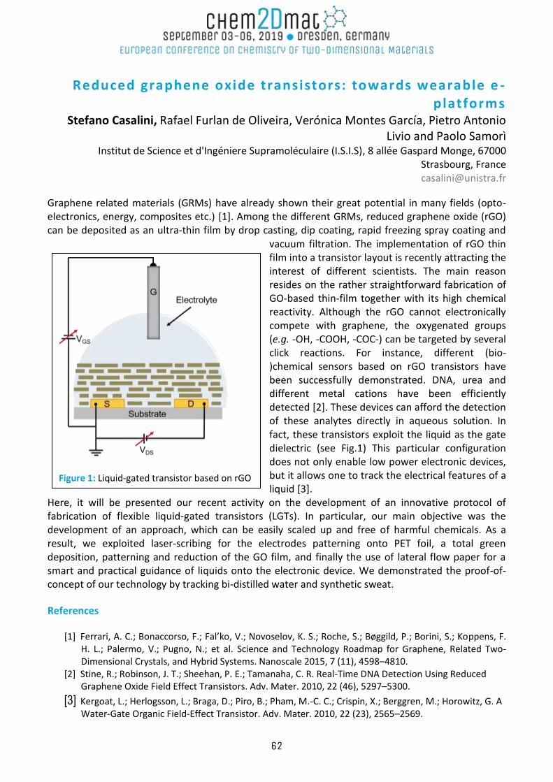
Reduced graphene oxide transistors: towards wearable e -platforms
Stefano Casalini, Rafael Furlan de Oliveira, Verónica Montes García, Pietro Antonio Livio and Paolo Samorì
Institut de Science et d'Ingéniere Supramoléculaire (I.S.I.S), 8 allée Gaspard Monge, 67000 Strasbourg, France
Graphene related materials (GRMs) have already shown their great potential in many fields (opto-electronics, energy, composites etc.) [1]. Among the different GRMs, reduced graphene oxide (rGO) can be deposited as an ultra-thin film by drop casting, dip coating, rapid freezing spray coating and
vacuum filtration. The implementation of rGO thin film into a transistor layout is recently attracting the interest of different scientists. The main reason resides on the rather straightforward fabrication of GO-based thin-film together with its high chemical reactivity. Although the rGO cannot electronically compete with graphene, the oxygenated groups (e.g. -OH, -COOH, -COC-) can be targeted by several click reactions. For instance, different (bio-)chemical sensors based on rGO transistors have been successfully demonstrated. DNA, urea and different metal cations have been efficiently detected [2]. These devices can afford the detection of these analytes directly in aqueous solution. In fact, these transistors exploit the liquid as the gate dielectric (see Fig.1) This particular configuration does not only enable low power electronic devices, but it allows one to track the electrical features of a liquid [3].
Here, it will be presented our recent activity on the development of an innovative protocol of fabrication of flexible liquid-gated transistors (LGTs). In particular, our main objective was the development of an approach, which can be easily scaled up and free of harmful chemicals. As a result, we exploited laser-scribing for the electrodes patterning onto PET foil, a total green deposition, patterning and reduction of the GO film, and finally the use of lateral flow paper for a smart and practical guidance of liquids onto the electronic device. We demonstrated the proof-of-concept of our technology by tracking bi-distilled water and synthetic sweat.
References
[1] Ferrari, A. C.; Bonaccorso, F.; Fal’ko, V.; Novoselov, K. S.; Roche, S.; Bøggild, P.; Borini, S.; Koppens, F. H. L.; Palermo, V.; Pugno, N.; et al. Science and Technology Roadmap for Graphene, Related Two-Dimensional Crystals, and Hybrid Systems. Nanoscale 2015, 7 (11), 4598–4810.
[2] Stine, R.; Robinson, J. T.; Sheehan, P. E.; Tamanaha, C. R. Real-Time DNA Detection Using Reduced Graphene Oxide Field Effect Transistors. Adv. Mater. 2010, 22 (46), 5297–5300.
[3] Kergoat, L.; Herlogsson, L.; Braga, D.; Piro, B.; Pham, M.-C. C.; Crispin, X.; Berggren, M.; Horowitz, G. A Water-Gate Organic Field-Effect Transistor. Adv. Mater. 2010, 22 (23), 2565–2569.
Figure 1: Liquid-gated transistor based on rGO
62
Chemical and Biomolecule Sensing using Graphene Field Effect Transistors
Jiri Cervenka Department of Thin Films and Nanostructures, FZU – Institute of Physics of The Czech Academy of
Sciences, Prague 16200, Czech Republic [email protected]
Graphene's two dimensional nature, highly sensitive unique electrical properties and low intrinsic noise characteristics make it a prime candidate for the creation of a new generation of molecular electronic sensors. Here we present a combined experimental and theoretical study of the electronic detection of different physisorbed biomolecules on graphene. Graphene field-effect transistors (GFETs) are used as a molecular sensors by measuring conductance changes as a function of gate voltage upon controlled adsorption of target molecules [1-3]. It is demonstrated that GFETs have a potential to measure distinct, coverage dependent, conductance signatures upon adsorption of small organic molecules in vacuum [1,2]. This method allowed electronic discrimination of individual DNA nucleobases on GFETs [1], providing a first step towards label-free graphene based electronic DNA sequencing. We compare electronic detection of different molecules on GFETs in vacuum, air and liquids and present various strategies for highly sensitive label-free electrical detection. To get a deeper insight into the origin of the sensing mechanism and molecular recognition in GFET measurements we also performed ab initio electronic structure calculations using density functional theory (DFT) [4,5]. The molecular recognition mechanism is found to be closely linked with specific noncovalent molecular interactions with graphene. We identify that the local electric fields induced by electric dipole moments and direct charge transfer play the dominant role in the modification of the electronic structure of graphene during the molecular detection. These effects open up a range of new opportunities for biomolecular recognition and enhancement of molecular sensitivity of graphene-based electronic sensors.
References
[1] N. Dontschuk, A. Stacey, A. Tadich, K. J. Rietwyk, A. Schenk, M. T. Edmonds, O. Shimoni, C. I. Pakes, S. Prawer, and J. Cervenka, Nature Communications 6, (2015) 6563.
[2] J. Cervenka, A. Budi, N. Dontschuk, A. Stacey, A. Tadich, K. J. Rietwyk, A. Schenk, M. T. Edmonds, Y. Yin, N. Medhekar, M. Kalbac, C. I. Pakes, Nanoscale 7, (2015) 1471 – 1478.
[3] H. Zhan, J. Cervenka, S. Prawer, D. J. Garrett, Molecular detection by liquid gated Hall effect measurement of graphene, Nanoscale 10, (2018) 930-935.
[4] Y. Yin, J. Cervenka and N. V. Medhekar, J. Phys. Chem. C, 119 (33), (2015) 19526–19534. [5] Y. Yin, J. Cervenka and N. V. Medhekar, J. Phys. Chem. Lett. 8 (13), (2017) 3087-3094.
63
Large-scale formation of s ingle -crystal one-third-hydrogenated graphene with anisotropic
e lectronic propert ies Hui Chen1,
De-Liang Bao 1, Dongfei Wang1, Yande Que1, Yu-Yang Zhang1,2, Wende Xiao 1, Shixuan Du,1* Sokrates T. Pantelides2,1, Hong-Jun Gao1*
1 Institute of Physics & University of Chinese Academy of Sciences, Chinese Academy of Sciences,
Beijing 100190, China. 2 Department of Physics and Astronomy and Department of Electrical Engineering and Computer
Science, Vanderbilt University, Nashville, Tennessee 37235, USA. [email protected]; [email protected]
It is generally thought that hydrogen atoms can chemisorb on graphene in a perfect periodic manner forming new crystalline two-dimensional (2D) materials that exhibit unique electronic properties beyond pristine graphene, such as graphene (fully hydrogenated graphene), graphone (half hydrogenated graphene) and 2D CxH y (other partially hydrogenated graphene). So far, samples with small patches of periodically-hydrogenated graphene can only be produced. In previous works, we have fabricated highly ordered, millimeter-scale, continuous single-crystalline graphene monolayer on Ru(0001) [1, 2], which provides a template for selective adsorption of atoms [3,4] or molecules [5]. Here, we use graphene/Ru(0001) as a temperate for hydrogenation. We present atomically resolved scanning tunneling microscope (STM) images and low-energy electron diffraction (LEED) patterns that demonstrate the fabrication of periodically-hydrogenated graphene that is perfectly ordered over 4 millimeters. The as-fabricated hydrogenated graphene is highly ordered, with a √3×√
3/R30° period relative to the pristine graphene. As the ratio of hydrogen and carbon is 1:3, the
periodically-hydrogenated graphene is named “ one-third-hydrogenated graphene”(OTHG).
Moreover, we show that, the OTHG is weakly coupled from the substrate and structurally anisotropic. Calculations show that the structural anisotropy of one-third hydrogenation results in an anisotropic electronic structure. This work provides an efficient method to produce large-scale crystalline functionalized graphene with specially desired properties. References
[1] Y. Pan, et al., Adv. Mater. 21 (2009) 2777. [2] Y. Pan, et al., Chin. Phys. 16 (2007) 3151 [3] J. D. Ren, et al., Nano Lett. 14 (2014) 4011 [4] J. D. Ren, et al., Phys. Rev. Lett. 119 (2017) 176806. [5] J. H. Mao, et al., J. Am. Chem. Soc. 131 (2009) 14136. [6] H. Chen, et al., Adv. Mater. 30 (2018) 1801838
64
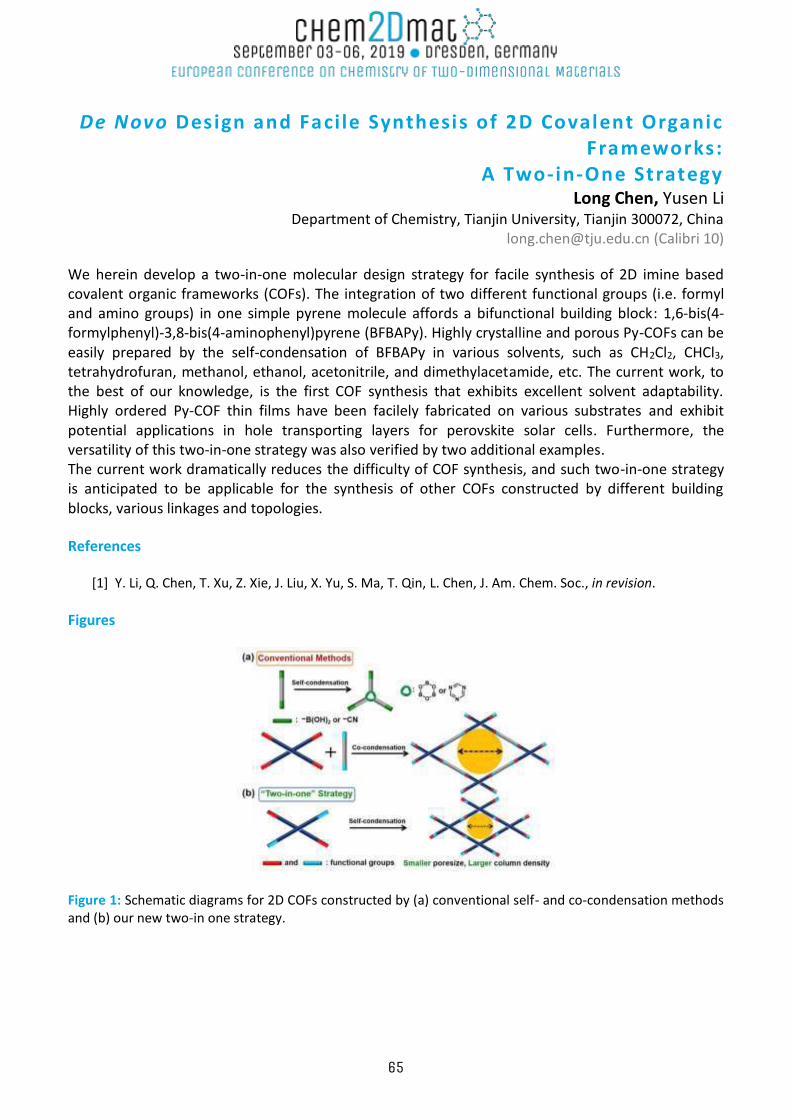
De Novo Design and Faci le Synthesis of 2D Covalent Organic Frameworks:
A Two-in-One Strategy Long Chen, Yusen Li
Department of Chemistry, Tianjin University, Tianjin 300072, China [email protected] (Calibri 10)
We herein develop a two-in-one molecular design strategy for facile synthesis of 2D imine based covalent organic frameworks (COFs). The integration of two different functional groups (i.e. formyl and amino groups) in one simple pyrene molecule affords a bifunctional building block: 1,6-bis(4-formylphenyl)-3,8-bis(4-aminophenyl)pyrene (BFBAPy). Highly crystalline and porous Py-COFs can be easily prepared by the self-condensation of BFBAPy in various solvents, such as CH2Cl2, CHCl3, tetrahydrofuran, methanol, ethanol, acetonitrile, and dimethylacetamide, etc. The current work, to the best of our knowledge, is the first COF synthesis that exhibits excellent solvent adaptability. Highly ordered Py-COF thin films have been facilely fabricated on various substrates and exhibit potential applications in hole transporting layers for perovskite solar cells. Furthermore, the versatility of this two-in-one strategy was also verified by two additional examples. The current work dramatically reduces the difficulty of COF synthesis, and such two-in-one strategy is anticipated to be applicable for the synthesis of other COFs constructed by different building blocks, various linkages and topologies. References
[1] Y. Li, Q. Chen, T. Xu, Z. Xie, J. Liu, X. Yu, S. Ma, T. Qin, L. Chen, J. Am. Chem. Soc., in revision.
Figures
Figure 1: Schematic diagrams for 2D COFs constructed by (a) conventional self- and co-condensation methods and (b) our new two-in one strategy.
65
Fluorescent Nitrogen -vacancy Diamond as VUV Sensor Bing-Ming Cheng
National Synchrotron Radiation Research Center, 101 Hsin-Ann Road, Hsinchu, Taiwan [email protected]
Abstract A natural or synthetic diamond might contain various point defects in its structure. If a diamond contain a nitrogen atom and a vacancy in its defect lattice as a pair at nearest-neighbour lattice sites, we name this point defect a nitrogen-vacancy (NV) center or defect. Among the various defects in diamond, the NV center might be most explored because of its prospective applications as an ultra-sensitive imaging sensor for external perturbations of mechanical stress, a combined nanoheater and nanothermometer in living cells, and a sensor of electric and magnetic field in biological environments. The NV-center diamonds have hence attracted many spectral investigations including optical absorption, photoluminescence (PL), electron paramagnetic resonance (EPR) and optically detected magnetic resonance (ODMR). In this work, photoluminescence spectra of fluorescent nitrogen-vacancy diamond (FNVD) containing NV0 and NV— defects near 300 K were investigated upon excitation in the range 30-525 nm. The emission of FNVD in wavelength range 540-850 nm for samples irradiated with light from a synchrotron source in wavelength range 30-200 nm has a nearly constant optical profile. PL excitation spectra in terms of the quantum yields for FNVD in wavelength region 30-300 nm were recorded on monitoring at 575, 620 and 682 nm. The quantum yields are above 0.13, with no window in the vacuum ultraviolet (VUV) region; we thus propose the use of FNVD as a VUV sensor. As a test, we measured the cross sections of gaseous O2 with sensor FNVD in wavelength region 115-200 nm and compared the results with data determined with sensor sodium salicylate (SS); the values obtained agree satisfactorily within 5 %. The results demonstrate that FNVD works successfully as a conventional SS sensor in the VUV region; moreover, the stability of FNVD is superior to that of SS. We conclude that applying FNVD as a VUV sensor has clearly several distinct advantages.
66
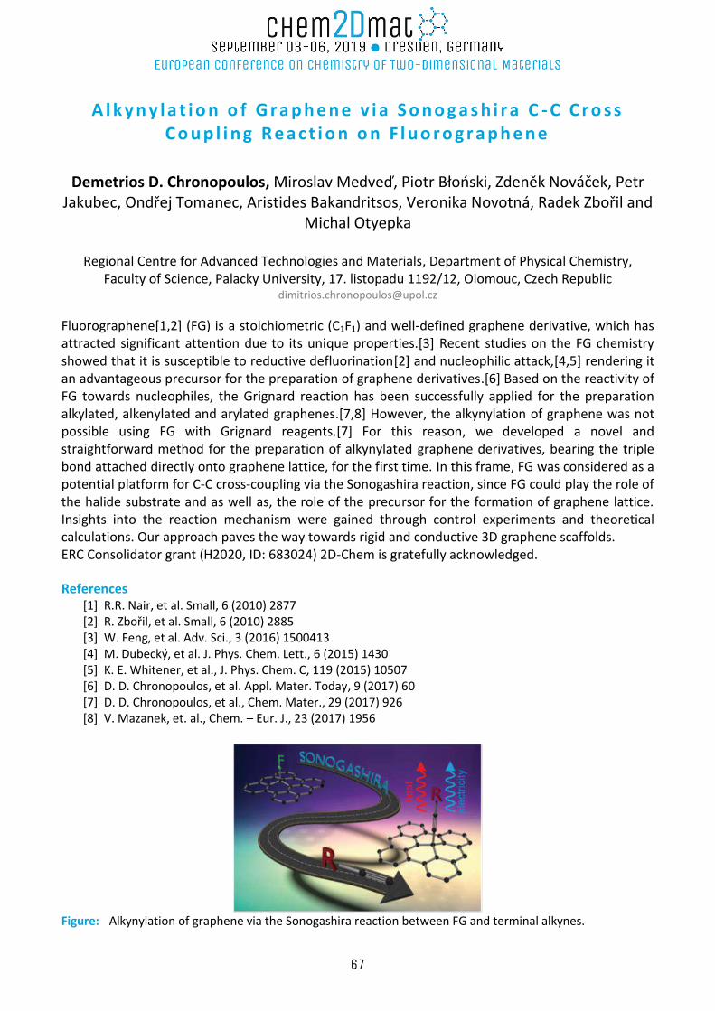
A l k y n y l a t i o n o f G r a p h e n e v i a S o n o g a s h i r a C - C C r o s s C o u p l i n g R e a c t i o n o n F l u o r o g r a p h e n e
Demetrios D. Chronopoulos, Miroslav Medveď, Piotr Błoński, Zdeněk Nováček, Petr
Jakubec, Ondřej Tomanec, Aristides Bakandritsos, Veronika Novotná, Radek Zbořil and Michal Otyepka
Regional Centre for Advanced Technologies and Materials, Department of Physical Chemistry,
Faculty of Science, Palacky University, 17. listopadu 1192/12, Olomouc, Czech Republic [email protected]
Fluorographene[1,2] (FG) is a stoichiometric (C1F1) and well-defined graphene derivative, which has attracted significant attention due to its unique properties.[3] Recent studies on the FG chemistry showed that it is susceptible to reductive defluorination[2] and nucleophilic attack,[4,5] rendering it an advantageous precursor for the preparation of graphene derivatives.[6] Based on the reactivity of FG towards nucleophiles, the Grignard reaction has been successfully applied for the preparation alkylated, alkenylated and arylated graphenes.[7,8] However, the alkynylation of graphene was not possible using FG with Grignard reagents.[7] For this reason, we developed a novel and straightforward method for the preparation of alkynylated graphene derivatives, bearing the triple bond attached directly onto graphene lattice, for the first time. In this frame, FG was considered as a potential platform for C-C cross-coupling via the Sonogashira reaction, since FG could play the role of the halide substrate and as well as, the role of the precursor for the formation of graphene lattice. Insights into the reaction mechanism were gained through control experiments and theoretical calculations. Our approach paves the way towards rigid and conductive 3D graphene scaffolds. ERC Consolidator grant (H2020, ID: 683024) 2D-Chem is gratefully acknowledged.
References [1] R.R. Nair, et al. Small, 6 (2010) 2877 [2] R. Zbořil, et al. Small, 6 (2010) 2885 [3] W. Feng, et al. Adv. Sci., 3 (2016) 1500413 [4] M. Dubecký, et al. J. Phys. Chem. Lett., 6 (2015) 1430 [5] K. E. Whitener, et al., J. Phys. Chem. C, 119 (2015) 10507 [6] D. D. Chronopoulos, et al. Appl. Mater. Today, 9 (2017) 60 [7] D. D. Chronopoulos, et al., Chem. Mater., 29 (2017) 926 [8] V. Mazanek, et. al., Chem. – Eur. J., 23 (2017) 1956
Figure: Alkynylation of graphene via the Sonogashira reaction between FG and terminal alkynes.
67
SPM studies on functionalizat ion of 2D transition metal dichalcogenides
Lakshya Daukiya1, Joan Teyssandier1, Samuel Eyley2, Salim El Kazzi3, Peter walke1, Wim
Thielemans2, Hiroshi Uji-i1 and Steven De Feyter1
1Division of Molecular Imaging and Photonics, Department of Chemistry, KU Leuven, Celestijnenlaan
200F, 3001 Leuven, Belgium. 2Renewable Materials and Nanotechnology Group, Department of Chemical Engineering, KU Leuven,
Campus Kortrijk, Etienne Sabbelaan 53, 8500 Kortrijk, Belgium 3imec, Kapeldreef 75, B-3001 Leuven, Belgium
Contact@ [email protected], [email protected]
Transition metal dichalcogenides (TMDs) are a new class of layered materials developed1 following the discovery of novel physical properties of graphene. Based on their composition and crystal structure TMDs can exhibit a wide range of electronic behavior from semiconducting to semimetallic, metallic and sometimes superconducting2. Tunability of the electronic bandstructure in these materials thus becomes important. Functionalization by covalent and non-covalent approach is a promising approach to effectively modify the electronic band gap, Fermi level position and induce doping in these materials3. In this work we will discuss about visualization of functionalized TMDs with scanning probe microscopy (SPM) techniques. We have carried out controlled covalent functionalization of TMDs by aryl diazonium chemistry which results in the formation of covalent bonds between for instance MoS2 and diazonium compounds. The grafted molecules on the TMDs are visualized using STM and AFM in ambient conditions. Additionally Raman and X-ray photoelectron spectroscopy were used to understand the impact of functionalization on the electronic properties of TMDs.
References
[1] Ruitao Lv, Joshua A. Robinson , Raymond E. Schaak , Du Sun ,Yifan Sun , Thomas E. Mallouk and Mauricio Terrones Acc. Chem. Res. 48, (2015), 56
[2] Sajedeh Manzeli, Dmitry Ovchinnikov, Diego Pasquier, Oleg V.Yazyev and Andras Kis Nature review
materials 2, (2017) 17033
[3] Stanislav Presolski and Martin Pumera Materials Today 19, (2016), 140
68
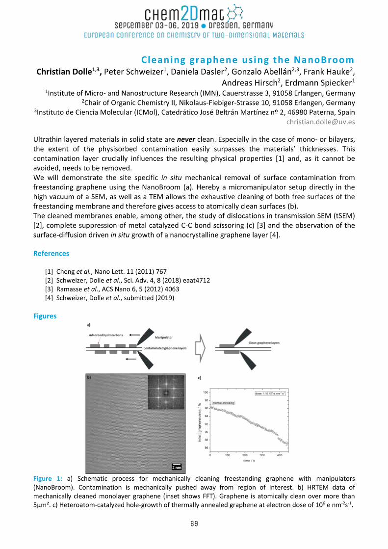
Cleaning graphene using the NanoBroom Christian Dolle1,3, Peter Schweizer1, Daniela Dasler2, Gonzalo Abellán2,3, Frank Hauke2,
Andreas Hirsch2, Erdmann Spiecker1 1Institute of Micro- and Nanostructure Research (IMN), Cauerstrasse 3, 91058 Erlangen, Germany
2Chair of Organic Chemistry II, Nikolaus-Fiebiger-Strasse 10, 91058 Erlangen, Germany 3Instituto de Ciencia Molecular (ICMol), Catedrático José Beltrán Martínez nº 2, 46980 Paterna, Spain
Ultrathin layered materials in solid state are never clean. Especially in the case of mono- or bilayers, the extent of the physisorbed contamination easily surpasses the materials’ thicknesses. This contamination layer crucially influences the resulting physical properties [1] and, as it cannot be avoided, needs to be removed. We will demonstrate the site specific in situ mechanical removal of surface contamination from freestanding graphene using the NanoBroom (a). Hereby a micromanipulator setup directly in the high vacuum of a SEM, as well as a TEM allows the exhaustive cleaning of both free surfaces of the freestanding membrane and therefore gives access to atomically clean surfaces (b). The cleaned membranes enable, among other, the study of dislocations in transmission SEM (tSEM) [2], complete suppression of metal catalyzed C-C bond scissoring (c) [3] and the observation of the surface-diffusion driven in situ growth of a nanocrystalline graphene layer [4].
References
[1] Cheng et al., Nano Lett. 11 (2011) 767 [2] Schweizer, Dolle et al., Sci. Adv. 4, 8 (2018) eaat4712 [3] Ramasse et al., ACS Nano 6, 5 (2012) 4063 [4] Schweizer, Dolle et al., submitted (2019)
Figures
Figure 1: a) Schematic process for mechanically cleaning freestanding graphene with manipulators (NanoBroom). Contamination is mechanically pushed away from region of interest. b) HRTEM data of mechanically cleaned monolayer graphene (inset shows FFT). Graphene is atomically clean over more than 5µm². c) Heteroatom-catalyzed hole-growth of thermally annealed graphene at electron dose of 106 e nm-2s-1.
69
Interfacia l Synthesis of 2D Conjugated Polymers: the Rise of Organic 2D Materials Renhao Dong, Xinliang Feng
Center for Advancing Electronics Dresden (cfaed) & Department of Chemistry and Food Chemistry, Technische Universität Dresden, Mommsenstrasse 4, 01062 Dresden, Germany
[email protected] The discovery of graphene one decade ago has triggered enormous interest in developing two-dimensional materials (2DMs). At present, various synthetic strategies have been devoted to produce 2DMs, such as top-down exfoliation and bottom-up chemical vapor deposition and solution synthesis.[1] In our work, we have employed the interfacial chemistry toward the controlled synthesis of organic 2D materials with varied structural features and diverse functions. For example, we demonstrated the synthesis of 2D conjugated metal-organic framework (2D c-MOF)―crystalline porous coordination polymer―at the air-water or liquid-liquid interfaces via metal-bis(dithiolene)/-bis(diimino)/-catecholate complexes. The resultant MOFs feature with large-area single layer or van der Waals stacked multi-layers and possess unique electronic properties, such as full delocalization of π-electrons, narrowed band gaps, largely improved conductivity and high charge mobility, which render 2D c-MOFs as advanced electroactive materials. One representative triphenylene-based iron-bis(dithiolene) MOF is a p-type semiconductor with a band-like transport and high charge mobility of ~220 cm2/Vs.[2] Currently, the 2D c-MOFs have been applied in transistors, sensing, magnetics, and energy storage and conversion.[3-5] In addition, we have also synthesized conjugated 2D covalent polymers, such as polyimines, polyimides and polypyrazines, at the air-water or liquid-liquid interfaces. For example, we synthesized a single-layer polycrystalline 2D polyimine at the air-water interface in a Langmuir-Blodget trough. The resultant 2D polyimine displayed an outstanding Young’s modulus (267±30 GPa) comparable to that of graphene and multi-functions in thin film field effect transistor (FET) and electrocatalytic water splitting.[6] In our latest work, by employing surfactant monolayer as a soft-template at the air-water interface, we were able to synthesize imide-based 2D polymers with highly ordered square units up to remarkable ~4 µm2 for a single crystalline domain. This preliminary result clearly highlights the feasibility to synthesize highly crystalline 2D polymers via soft-template-assisted interfacial synthesis strategy. In short, we expect to develop interfacial chemistry toward the synthetic 2DMs and achieve delineation of reliable chemistry-structure-property relationships and superior physical and chemical performances.
References
[1] R. Dong, T. Zhang and X. Feng*, Chem. Rev. 118 (2018), 6189-6235. [2] R. Dong…X. Feng*, et al., Nat. Mater. 17 (2018), 1027-1032. [3] R. Dong…X. Feng*, et al., Nat. Commun. 9 (2018), 2637. [4] H. Zhong…R.Dong*, X. Feng*, et al., Angew. Chem. Int. Ed. 2019, DOI: 10.1002/ange.201907002. [5] C. Yang, R. Dong*…X. Feng*, et al., Nat. Commun. 2019, DOI: 10.1038/s41467-019-11267-w. [6] H. Sahabudeen…R. Dong…X. Feng*, et al., Nat. Commun. 7 (2016), 13461.
70
Fabrication of large-scale graphene/2D-germanium heterostructure by intercalation
Hui Guo, Hongliang Lu, De-Liang Bao, Xueyan Wang, Geng Li, Yu-Yang Zhang, Shixuan Du,*
Hong-Jun Gao*
Institute of Physics & University of Chinese Academy of Sciences, Chinese Academy of Sciences, Beijing 100190, China.
[email protected]; [email protected]
Heterostructures based on graphene and two-dimensional (2D) materials not only exhibit fascinating properties and potential applications, but also provide new horizons to the research of graphene. Our previous work show that we have successfully fabricated graphene/silicene van der Waals heterostructure, which exhibit Schottky rectification behavior. Here we report a large-scale, high-quality heterostructure composed of vertically-stacked graphene and two-dimensional (2D) germanium. The heterostructure is constructed by intercalation-assisted technique. We first synthesize large-scale, single-crystalline graphene on Ir(111) surface and then intercalate germanium at the interface of graphene and Ir(111). The intercalated germanium forms a well-defined 2D layer with a 2 × 2 superstructure with respect to Ir(111). Theoretical calculations demonstrate that the 2D germanium has a double-layer structure. Raman characterizations show the 2D germanium effectively weakens the interaction between graphene and Ir substrate, making graphene more like intrinsic one. Further experiments of low-energy electron diffraction, scanning tunneling microscopy, and X-ray photoelectron spectroscopy confirm the formation of large-scale and high-quality graphene/2D-germanium vertical heterostructure. The integration of graphene with a traditional 2D semiconductor provides a platform to explore new physical phenomena in the future. References
[1] J. H. Mao, et al., Appl. Phys. Lett. 100 (2012) 093101 [2] G. Li, et al., J. Am. Chem. Soc. 137 (2015) 7099 [3] G. Li, et al., Adv. Mater. 30 (2018) 1804650 [4] G. Li, et al., Chem. Soc. Rev. 47 (2018) 982 [5] H. Guo, et al., Chin. Phys. B 28 (2019) 078103
71
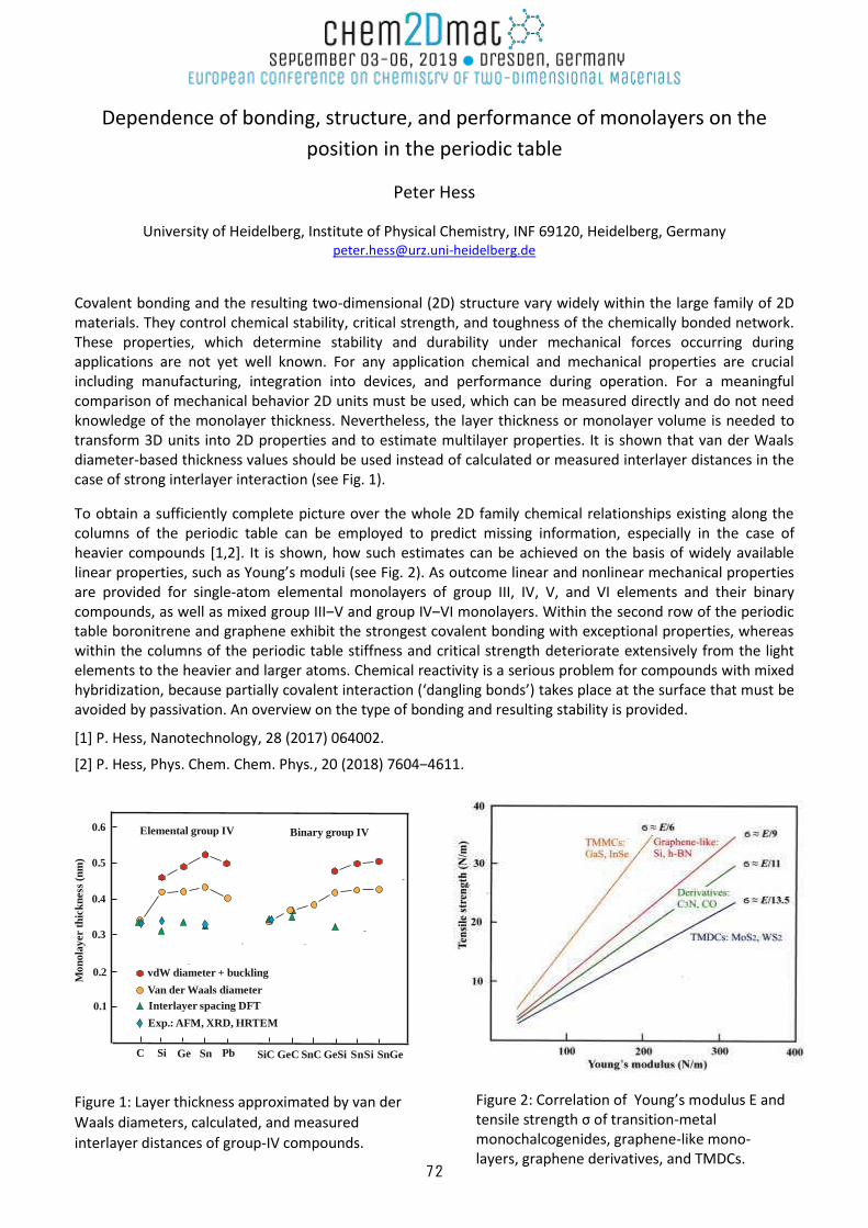
Dependence of bonding, structure, and performance of monolayers on the
position in the periodic table
Peter Hess
University of Heidelberg, Institute of Physical Chemistry, INF 69120, Heidelberg, Germany [email protected]
Covalent bonding and the resulting two-dimensional (2D) structure vary widely within the large family of 2D materials. They control chemical stability, critical strength, and toughness of the chemically bonded network. These properties, which determine stability and durability under mechanical forces occurring during applications are not yet well known. For any application chemical and mechanical properties are crucial including manufacturing, integration into devices, and performance during operation. For a meaningful comparison of mechanical behavior 2D units must be used, which can be measured directly and do not need knowledge of the monolayer thickness. Nevertheless, the layer thickness or monolayer volume is needed to transform 3D units into 2D properties and to estimate multilayer properties. It is shown that van der Waals diameter-based thickness values should be used instead of calculated or measured interlayer distances in the case of strong interlayer interaction (see Fig. 1).
To obtain a sufficiently complete picture over the whole 2D family chemical relationships existing along the columns of the periodic table can be employed to predict missing information, especially in the case of heavier compounds [1,2]. It is shown, how such estimates can be achieved on the basis of widely available linear properties, such as Young’s moduli (see Fig. 2). As outcome linear and nonlinear mechanical properties are provided for single-atom elemental monolayers of group III, IV, V, and VI elements and their binary compounds, as well as mixed group III‒V and group IV‒VI monolayers. Within the second row of the periodic table boronitrene and graphene exhibit the strongest covalent bonding with exceptional properties, whereas within the columns of the periodic table stiffness and critical strength deteriorate extensively from the light elements to the heavier and larger atoms. Chemical reactivity is a serious problem for compounds with mixed hybridization, because partially covalent interaction (‘dangling bonds’) takes place at the surface that must be avoided by passivation. An overview on the type of bonding and resulting stability is provided.
[1] P. Hess, Nanotechnology, 28 (2017) 064002.
[2] P. Hess, Phys. Chem. Chem. Phys., 20 (2018) 7604‒4611.
C Si Ge Sn SiC GeC SnC GeSi
Elemental group IV Binary group IV
Van der Waals diameter
Interlayer spacing DFT0.1
0.2
0.3
0.4
0.5
Mon
ola
yer
thic
kn
ess
(n
m)
Exp.: AFM, XRD, HRTEM
vdW diameter + buckling
0.6
Pb SnSi SnGe
Figure 1: Layer thickness approximated by van der
Waals diameters, calculated, and measured
interlayer distances of group-IV compounds.
Figure 2: Correlation of Young’s modulus E and tensile strength σ of transition-metal monochalcogenides, graphene-like mono-layers, graphene derivatives, and TMDCs.
72
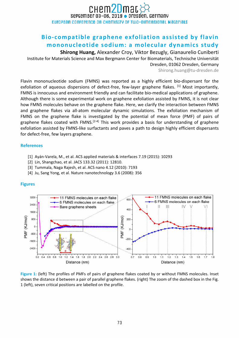
Bio-compatible graphene exfol iat ion assisted by f lavin mononucleotide sodium: a molecular dynamics study
Shirong Huang, Alexander Croy, Viktor Bezugly, Gianaurelio Cuniberti Institute for Materials Science and Max Bergmann Center for Biomaterials, Technische Universität
Dresden, 01062 Dresden, Germany [email protected]
Flavin mononucleotide sodium (FMNS) was reported as a highly efficient bio-dispersant for the exfoliation of aqueous dispersions of defect-free, few-layer graphene flakes. [1] Most importantly, FMNS is innocuous and environment friendly and can facilitate bio-medical applications of graphene. Although there is some experimental work on graphene exfoliation assisted by FMNS, it is not clear how FMNS molecules behave on the graphene flake. Here, we clarify the interaction between FMNS and graphene flakes via all-atom molecular dynamic simulations. The exfoliation mechanism of FMNS on the graphene flake is investigated by the potential of mean force (PMF) of pairs of graphene flakes coated with FMNS.[2-4] This work provides a basis for understanding of graphene exfoliation assisted by FMNS-like surfactants and paves a path to design highly efficient dispersants for defect-free, few layers graphene. References
[1] Ayán-Varela, M., et al. ACS applied materials & interfaces 7.19 (2015): 10293 [2] Lin, Shangchao, et al. JACS 133.32 (2011): 12810. [3] Tummala, Naga Rajesh, et al. ACS nano 4.12 (2010): 7193 [4] Ju, Sang Yong, et al. Nature nanotechnology 3.6 (2008): 356
Figures
Figure 1: (left) The profiles of PMFs of pairs of graphene flakes coated by or without FMNS molecules. Inset shows the distance d between a pair of parallel graphene flakes. (right) The zoom of the dashed box in the Fig. 1 (left), seven critical positions are labelled on the profile.
73
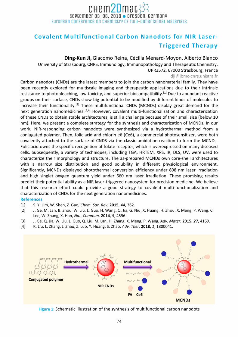
Covalent Multi functional Carbon Nanodots for NIR Laser-
Triggered Therapy
Ding-Kun Ji, Giacomo Reina, Cécilia Ménard-Moyon, Alberto Bianco University of Strasbourg, CNRS, Immunology, Immunopathology and Therapeutic Chemistry,
UPR3572, 67000 Strasbourg, France [email protected]
Carbon nanodots (CNDs) are the latest members to join the carbon nanomaterial family. They have been recently explored for multiscale imaging and therapeutic applications due to their intrinsic resistance to photobleaching, low toxicity, and superior biocompatibility.[1] Due to abundant reactive groups on their surface, CNDs show big potential to be modified by different kinds of molecules to increase their functionality.[2] These multifunctional CNDs (MCNDs) display great demand for the next generation nanomedicines.[3,4] However, covalent multi-functionalization and characterization of these CNDs to obtain stable architectures, is still a challenge because of their small size (below 10 nm). Here, we present a complete strategy for the synthesis and characterization of MCNDs. In our work, NIR-responding carbon nanodots were synthesized via a hydrothermal method from a conjugated polymer. Then, folic acid and chlorin e6 (Ce6), a commercial photosensitizer, were both covalently attached to the surface of CNDS via the classic amidation reaction to form the MCNDs. Folic acid owns the specific recognition of folate receptor, which is overexpressed on many diseased cells. Subsequently, a variety of techniques, including TGA, HRTEM, XPS, IR, DLS, UV, were used to characterize their morphology and structure. The as-prepared MCNDs own core-shell architectures with a narrow size distribution and good solubility in different physiological environment. Significantly, MCNDs displayed photothermal conversion efficiency under 808 nm laser irradiation and high singlet oxygen quantum yield under 660 nm laser irradiation. These promising results predict their potential ability as a NIR laser-triggered nanosystem for precision medicine. We believe that this research effort could provide a good strategy to covalent multi-functionalization and characterization of CNDs for the next generation nanomedicines. References [1] S. Y. Lim, W. Shen, Z. Gao, Chem. Soc. Rev. 2015, 44, 362. [2] J. Ge, M. Lan, B. Zhou, W. Liu, L. Guo, H. Wang, Q. Jia, G. Niu, X. Huang, H. Zhou, X. Meng, P. Wang, C.
Lee, W. Zhang, X. Han, Nat. Commun. 2014, 5, 4596. [3] J. Ge, Q. Jia, W. Liu, L. Guo, Q. Liu, M. Lan, H. Zhang, X. Meng, P. Wang, Adv. Mater. 2015, 27, 4169. [4] R. Liu, L. Zhang, J. Zhao, Z. Luo, Y. Huang, S. Zhao, Adv. Ther. 2018, 1, 1800041.
MultifunctionalHydrothermal
Conjugated polymer
MCNDs
NIR CNDs
FA Ce6
Figure 1: Schematic illustration of the synthesis of multifunctional carbon nanodots
74
Graphene functional izat ion for bui lding of complex structures, nanoscale motion and resist free patterning
Martin Kalbac, Petr Kovaricek, Karolina Drogowska, Jan Plsek, Zdenek Bastl J. Heyrovsky Institute of Physical Chemistry, Dolejškova 2155/3, 182 23 Prague, CR
We discuss functionalization of graphene as a tool to rationally construct more complex systems, induce motion on nanoscale and to enable resist free patterning. The application of functional groups for rational building of complex systems is demonstrated on the heterostructure composed of CVD grown graphene and the PEDOT. The graphene was first functionalized by sulfonate and subsequently oxidative polymerization of EDOT has been performed on the functionalized graphene surface. This approach enabled to control each preparation step and to study how the properties of graphene interface are changing. Also we implemented dynamic covalent chemistry for directional motion of fluorescent nanodiamond particles at a functionalized graphene surface via imine linkages. The dynamic connections allowed for controlling the formation and rupture of these linkages by external stimuli. By introduction of pH gradients, the nanoparticles were driven to move along the gradient due to the different rates of the imine condensation and hydrolysis in the two environments. Finally, resist free patterning is demonstrated by combination of two competing reactions on a graphene substrate. For this we applied photo-modulated Mitsunobu reaction on oxygenated graphene, which serves both as the substrate for introduction of carboxylate species as well as reagent in the reductive de-oxygenation by triphenylphosphine (PPh3).
References
[1] P. Kovaříček, K. Drogowska, Z. Melníková Komínková, V. Blechta, Z. Bastl, D. Gromadzki, M. Fridrichová, M. Kalbáč, Carbon,113 (2017) 33.
[2] P. Kovaříček, V. Vrkoslav, J. Plšek, Z. Bastl, M. Fridrichová, K. Drogowska M. Kalbáč, Carbon,118 (2017) 200.
[3] I.Matulková, P. Kovaříček, M. Šlouf, I. Němec, M. Kalbáč, Carbon,124 (2017) 250.
[4] P. Kovaříček, M. Cebecauer, J. Neburková, J. Bartoň,M. Fridrichová, K. A. Drogowska, P. Cigler, J.-M. Lehn, and M. Kalbac: ACS Nano, 12 (2018) 7141.
[5] L. Valenta, P. Kovaricek, V. Vales, Z. Bastl, Karolina A. Drogowska, T. A. Verhagen, R. Cibulka, and M. Kalbac : Spatially Resolved Covalent Functionalization Patterns on Graphene, Angew. Chem. Int. Ed., 58 (2019) 1324.
75
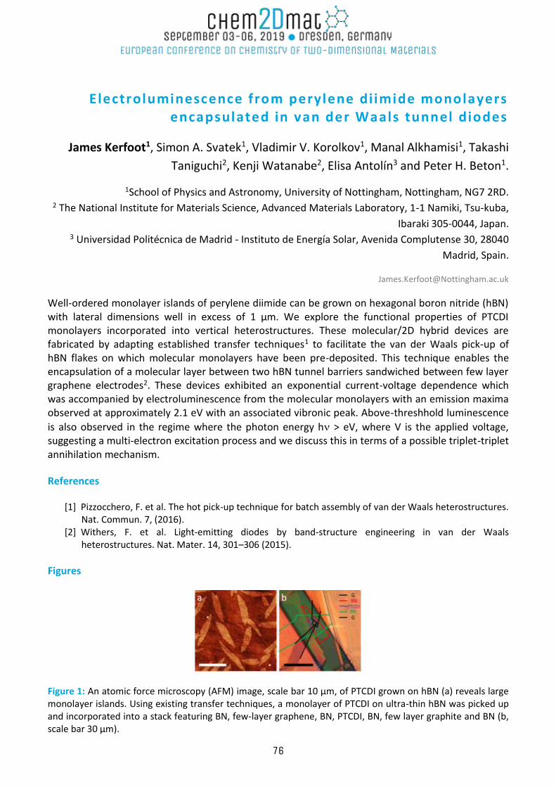
Electroluminescence from perylene di imide monolayers encapsulated in van der Waals tunnel diodes
James Kerfoot1, Simon A. Svatek1, Vladimir V. Korolkov1, Manal Alkhamisi1, Takashi
Taniguchi2, Kenji Watanabe2, Elisa Antolín3 and Peter H. Beton1.
1School of Physics and Astronomy, University of Nottingham, Nottingham, NG7 2RD. 2 The National Institute for Materials Science, Advanced Materials Laboratory, 1-1 Namiki, Tsu-kuba,
Ibaraki 305-0044, Japan. 3 Universidad Politécnica de Madrid - Instituto de Energía Solar, Avenida Complutense 30, 28040
Madrid, Spain.
Well-ordered monolayer islands of perylene diimide can be grown on hexagonal boron nitride (hBN) with lateral dimensions well in excess of 1 µm. We explore the functional properties of PTCDI monolayers incorporated into vertical heterostructures. These molecular/2D hybrid devices are fabricated by adapting established transfer techniques1 to facilitate the van der Waals pick-up of hBN flakes on which molecular monolayers have been pre-deposited. This technique enables the encapsulation of a molecular layer between two hBN tunnel barriers sandwiched between few layer graphene electrodes2. These devices exhibited an exponential current-voltage dependence which was accompanied by electroluminescence from the molecular monolayers with an emission maxima observed at approximately 2.1 eV with an associated vibronic peak. Above-threshhold luminescence
is also observed in the regime where the photon energy h > eV, where V is the applied voltage, suggesting a multi-electron excitation process and we discuss this in terms of a possible triplet-triplet annihilation mechanism.
References
[1] Pizzocchero, F. et al. The hot pick-up technique for batch assembly of van der Waals heterostructures. Nat. Commun. 7, (2016).
[2] Withers, F. et al. Light-emitting diodes by band-structure engineering in van der Waals heterostructures. Nat. Mater. 14, 301–306 (2015).
Figures
Figure 1: An atomic force microscopy (AFM) image, scale bar 10 µm, of PTCDI grown on hBN (a) reveals large monolayer islands. Using existing transfer techniques, a monolayer of PTCDI on ultra-thin hBN was picked up and incorporated into a stack featuring BN, few-layer graphene, BN, PTCDI, BN, few layer graphite and BN (b, scale bar 30 µm).
76
Ultrathin Two-Dimensional Cobalt Zeolite-Imidazole Framework Nanosheets for Electrocatalytic Oxygen Evolution
Kolleboyina Jayaramulu, Radek Zboril, and Roland A. Fischer
Department of Chemistry and Catalysis Research Centre, Technical University of Munich, 85748 Garching, Germany Regional Centre of Advanced Technologies and Materials, Faculty of Science, Palacky University, Šlechtitelů 27, 783 71, Olomouc, Czech Republic. Email: [email protected]
A promising class of novel systems are 2D inorganic-organic hybrid materials derived from crystalline coordination networks, in particular from metal-organic frameworks (MOFs). In general, MOFs are based on the self-assembly of metal ions and organic linkers to yield 3-dimesional crystalline porous coordination networks.[1-4] MOFs may feature highly exposed active sites on their surface, including coordinatively unsaturated metal sites suited as catalytic reaction centres. Thus, 2D MOFs offer humongous possibilities and a wide parameter space, allowing for eventually achieving superior and unusual material properties that cannot be obtained otherwise. 2D MOFs exhibit a layered structure with strong in-plane coordination bonds and weak interactions between the layers (e.g., van der Waals forces and hydrogen bonding). This property may provide favorable interaction between active sites and substrate molecules with a smaller diffusion barrier as compared to their 3D bulk MOF counter parts. In my presentation, I would like to discuss on my recent paper on unprecedented facile and scalable strategy to obtain cobalt zeolite imidazole framework 2D layers by liquid exfoliation of the ZIF-9(III) phase and it exhibited highly efficient OER activity in alkaline medium.[5]
References
[1] K. Jayaramulu, F. Geyer, A. Schneemann, Š. Kment, M. Otyepka, R. Zboril, D. Vollmer, R. A. Fischer,
Adv.Mater. 2019, 0, 1900820.
[2] D. P. Dubal, K. Jayaramulu, J. Sunil, Š. Kment, P. Gomez-Romero, C. Narayana, R. Zbořil, R. A. Fischer,
Adv. Funct. Mater. 2019, 0, 1900532.
[3] K. Jayaramulu, D. P. Dubal, B. Nagar, V. Ranc, O. Tomanec, M. Petr, K. K. R. Datta, R. Zboril, P. Gomez-
Romero, R. A. Fischer, Adv. Mater. 2018, 30, e1705789.
[4] K. Jayaramulu, J. Masa, O. Tomanec, D. Peeters, V. Ranc, A. Schneemann, R. Zboril, W. Schuhmann, R.
A. Fischer, Adv. Funct. Mater. 2017, 27.
[5] K. Jayaramulu, J. Masa, D. M. Morales, O. Tomanec, V. Ranc, M. Petr, P. Wilde, Y. T. Chen, R. Zboril, W.
Schuhmann, R. A. Fischer, Adv. Sci. 2018.
77
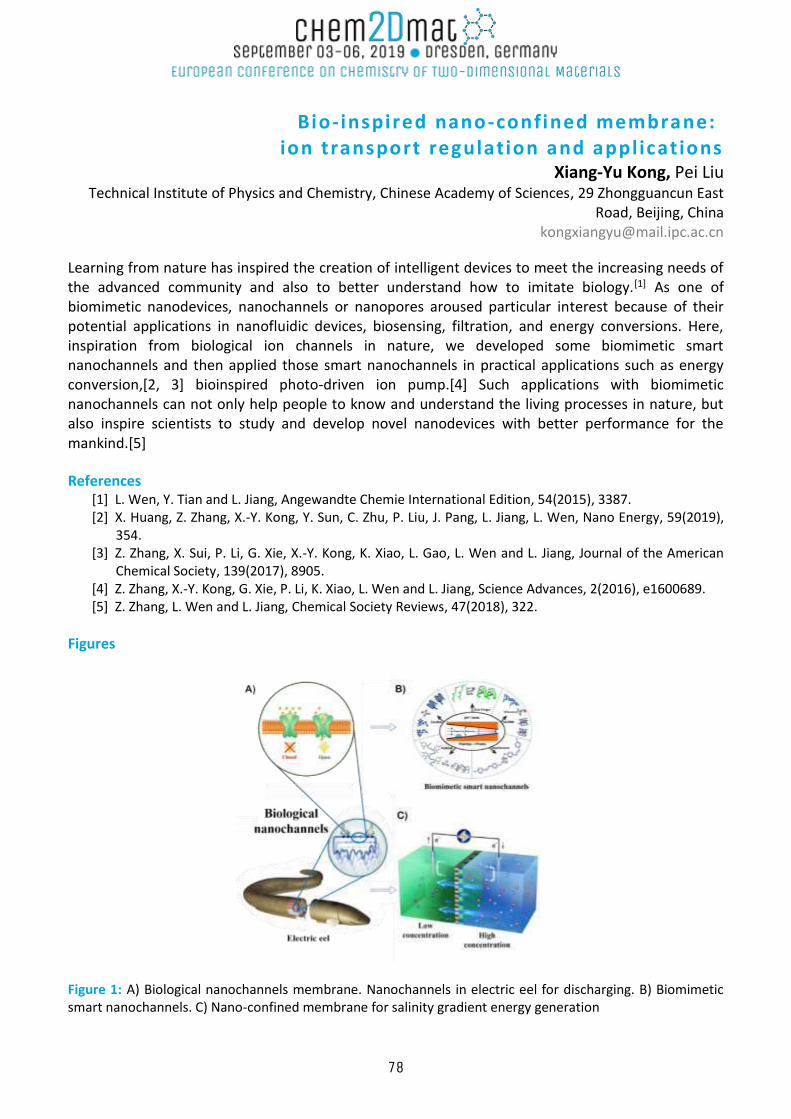
Bio-inspired nano-confined membrane: ion transport regulation and applicat ions
Xiang-Yu Kong, Pei Liu Technical Institute of Physics and Chemistry, Chinese Academy of Sciences, 29 Zhongguancun East
Road, Beijing, China [email protected]
Learning from nature has inspired the creation of intelligent devices to meet the increasing needs of the advanced community and also to better understand how to imitate biology.[1] As one of biomimetic nanodevices, nanochannels or nanopores aroused particular interest because of their potential applications in nanofluidic devices, biosensing, filtration, and energy conversions. Here, inspiration from biological ion channels in nature, we developed some biomimetic smart nanochannels and then applied those smart nanochannels in practical applications such as energy conversion,[2, 3] bioinspired photo-driven ion pump.[4] Such applications with biomimetic nanochannels can not only help people to know and understand the living processes in nature, but also inspire scientists to study and develop novel nanodevices with better performance for the mankind.[5]
References [1] L. Wen, Y. Tian and L. Jiang, Angewandte Chemie International Edition, 54(2015), 3387. [2] X. Huang, Z. Zhang, X.-Y. Kong, Y. Sun, C. Zhu, P. Liu, J. Pang, L. Jiang, L. Wen, Nano Energy, 59(2019),
354. [3] Z. Zhang, X. Sui, P. Li, G. Xie, X.-Y. Kong, K. Xiao, L. Gao, L. Wen and L. Jiang, Journal of the American
Chemical Society, 139(2017), 8905. [4] Z. Zhang, X.-Y. Kong, G. Xie, P. Li, K. Xiao, L. Wen and L. Jiang, Science Advances, 2(2016), e1600689. [5] Z. Zhang, L. Wen and L. Jiang, Chemical Society Reviews, 47(2018), 322.
Figures
Figure 1: A) Biological nanochannels membrane. Nanochannels in electric eel for discharging. B) Biomimetic smart nanochannels. C) Nano-confined membrane for salinity gradient energy generation
78
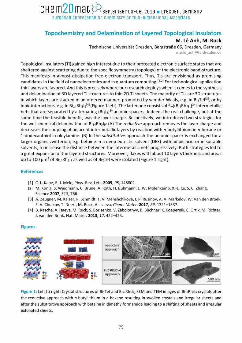
Topochemistry and Delamination of Layered Topological Insulators M. Lê Anh, M. Ruck
Technische Universität Dresden, Bergstraße 66, Dresden, Germany [email protected]
Topological insulators (TI) gained high interest due to their protected electronic surface states that are sheltered against scattering due to the specific symmetry (topology) of the electronic band-structure. This manifests in almost dissipation-free electron transport. Thus, TIs are envisioned as promising candidates in the field of nanoelectronics and in quantum computing.[1,2] For technological application thin layers are favored. And this is precisely where our research deploys when it comes to the synthesis and delamination of 3D layered TI structures to thin 2D TI sheets. The majority of TIs are 3D structures in which layers are stacked in an ordered manner, promoted by van-der-Waals, e.g. in Bi2TeI[3], or by ionic interactions, e.g. in Bi14Rh3I9
[4] (Figure 1 left). The latter one consists of 2∞[(Bi4Rh)3I]2+ intermetallic
nets that are separated by alternating (Bi2I8)2– anionic spacers. Indeed, the real challenge, but at the same time the feasible benefit, was the layer charge. Respectively, we introduced two strategies for the wet-chemical delamination of Bi14Rh3I9: (A) The reductive approach removes the layer charge and decreases the coupling of adjacent intermetallic layers by reaction with n-butyllithium in n-hexane or 1-dodecanthiol in oleylamine. (B) In the substitutive approach the anionic spacer is exchanged for a larger organic zwitterion, e.g. betaine in a deep eutectic solvent (DES) with adipic acid or in suitable solvents, to increase the distance between the intermetallic nets progressively. Both strategies led to a great expansion of the layered structures. Moreover, flakes with about 10 layers thickness and areas up to 100 µm2 of Bi14Rh3I9 as well as of Bi2TeI were isolated (Figure 1 right). References
[1] C. L. Kane, E. J. Mele, Phys. Rev. Lett. 2005, 95, 146802. [2] M. König, S. Wiedmann, C. Brüne, A. Roth, H. Buhmann, L. W. Molenkamp, X.-L. Qi, S. C. Zhang,
Science 2007, 318, 766. [3] A. Zeugner, M. Kaiser, P. Schmidt, T. V. Menshchikova, I. P. Rusinov, A. V. Markelov, W. Van den Broek,
E. V. Chulkov, T. Doert, M. Ruck, A. Isaeva, Chem. Mater. 2017, 29, 1321–1337. [4] B. Rasche, A. Isaeva, M. Ruck, S. Borisenko, V. Zabolotnyy, B. Büchner, K. Koepernik, C. Ortix, M. Richter,
J. van den Brink, Nat. Mater. 2013, 12, 422–425.
Figures
Figure 1: Left to right: Crystal structures of Bi2TeI and Bi14Rh3I9; SEM and TEM images of Bi14Rh3I9 crystals after
the reductive approach with n-butyllithium in n-hexane resulting in swollen crystals and irregular sheets and
after the substitutive approach with betaine in dimethylformamide leading to a shifting of sheets and irregular
exfoliated sheets.
79
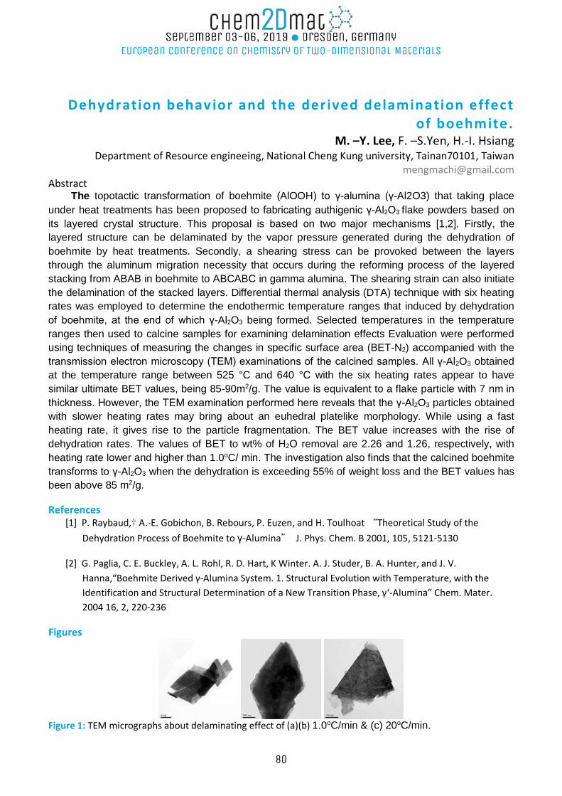
Dehydration behavior and the derived delamination effect
of boehmite. M. –Y. Lee, F. –S.Yen, H.-I. Hsiang
Department of Resource engineeing, National Cheng Kung university, Tainan70101, Taiwan [email protected]
Abstract The topotactic transformation of boehmite (AlOOH) to γ-alumina (γ-Al2O3) that taking place
under heat treatments has been proposed to fabricating authigenic γ-Al2O3 flake powders based on
its layered crystal structure. This proposal is based on two major mechanisms [1,2]. Firstly, the
layered structure can be delaminated by the vapor pressure generated during the dehydration of
boehmite by heat treatments. Secondly, a shearing stress can be provoked between the layers
through the aluminum migration necessity that occurs during the reforming process of the layered
stacking from ABAB in boehmite to ABCABC in gamma alumina. The shearing strain can also initiate
the delamination of the stacked layers. Differential thermal analysis (DTA) technique with six heating
rates was employed to determine the endothermic temperature ranges that induced by dehydration
of boehmite, at the end of which γ-Al2O3 being formed. Selected temperatures in the temperature
ranges then used to calcine samples for examining delamination effects Evaluation were performed
using techniques of measuring the changes in specific surface area (BET-N2) accompanied with the
transmission electron microscopy (TEM) examinations of the calcined samples. All γ-Al2O3 obtained
at the temperature range between 525 °C and 640 °C with the six heating rates appear to have
similar ultimate BET values, being 85-90m2/g. The value is equivalent to a flake particle with 7 nm in
thickness. However, the TEM examination performed here reveals that the γ-Al2O3 particles obtained
with slower heating rates may bring about an euhedral platelike morphology. While using a fast
heating rate, it gives rise to the particle fragmentation. The BET value increases with the rise of
dehydration rates. The values of BET to wt% of H2O removal are 2.26 and 1.26, respectively, with
heating rate lower and higher than 1.0oC/ min. The investigation also finds that the calcined boehmite
transforms to γ-Al2O3 when the dehydration is exceeding 55% of weight loss and the BET values has
been above 85 m2/g.
References [1] P. Raybaud,† A.-E. Gobichon, B. Rebours, P. Euzen, and H. Toulhoat “Theoretical Study of the
Dehydration Process of Boehmite to γ-Alumina” J. Phys. Chem. B 2001, 105, 5121-5130
[2] G. Paglia, C. E. Buckley, A. L. Rohl, R. D. Hart, K Winter. A. J. Studer, B. A. Hunter, and J. V.
Hanna,“Boehmite Derived γ-Alumina System. 1. Structural Evolution with Temperature, with the
Identification and Structural Determination of a New Transition Phase, γ‘-Alumina” Chem. Mater.
2004 16, 2, 220-236
Figures
Figure 1: TEM micrographs about delaminating effect of (a)(b) 1.0oC/min & (c) 20oC/min.
80
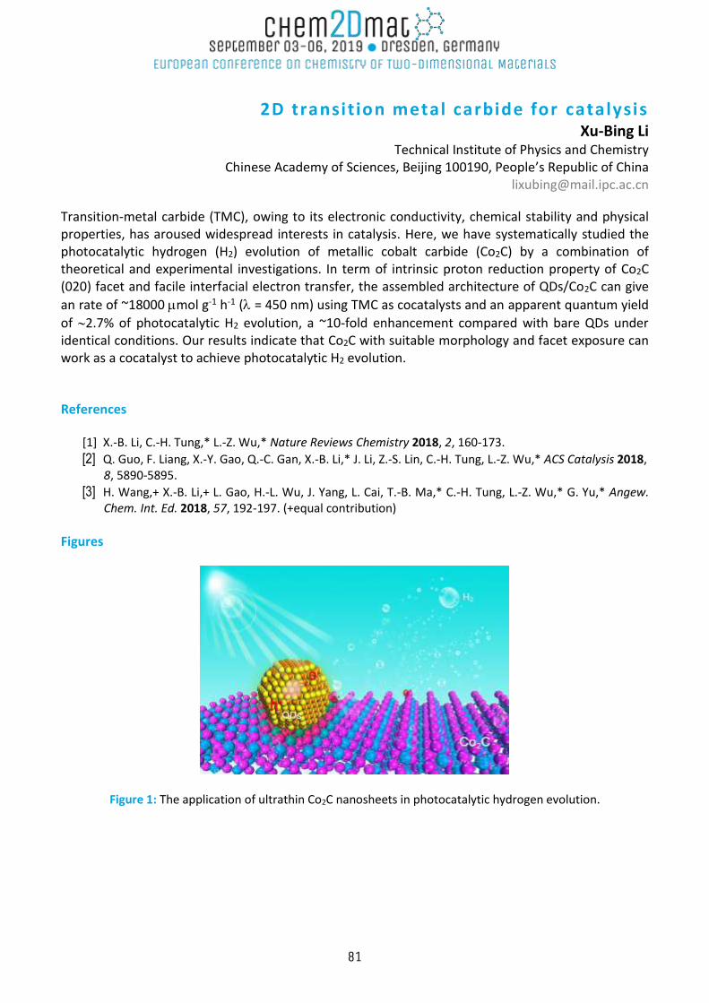
2D transition metal carbide for catalysis Xu-Bing Li
Technical Institute of Physics and Chemistry Chinese Academy of Sciences, Beijing 100190, People’s Republic of China
Transition-metal carbide (TMC), owing to its electronic conductivity, chemical stability and physical properties, has aroused widespread interests in catalysis. Here, we have systematically studied the photocatalytic hydrogen (H2) evolution of metallic cobalt carbide (Co2C) by a combination of theoretical and experimental investigations. In term of intrinsic proton reduction property of Co2C (020) facet and facile interfacial electron transfer, the assembled architecture of QDs/Co2C can give
an rate of ~18000 mol g-1 h-1 ( = 450 nm) using TMC as cocatalysts and an apparent quantum yield
of 2.7% of photocatalytic H2 evolution, a ~10-fold enhancement compared with bare QDs under identical conditions. Our results indicate that Co2C with suitable morphology and facet exposure can work as a cocatalyst to achieve photocatalytic H2 evolution.
References
[1] X.-B. Li, C.-H. Tung,* L.-Z. Wu,* Nature Reviews Chemistry 2018, 2, 160-173.
[2] Q. Guo, F. Liang, X.-Y. Gao, Q.-C. Gan, X.-B. Li,* J. Li, Z.-S. Lin, C.-H. Tung, L.-Z. Wu,* ACS Catalysis 2018, 8, 5890-5895.
[3] H. Wang,+ X.-B. Li,+ L. Gao, H.-L. Wu, J. Yang, L. Cai, T.-B. Ma,* C.-H. Tung, L.-Z. Wu,* G. Yu,* Angew. Chem. Int. Ed. 2018, 57, 192-197. (+equal contribution)
Figures
Figure 1: The application of ultrathin Co2C nanosheets in photocatalytic hydrogen evolution.
81
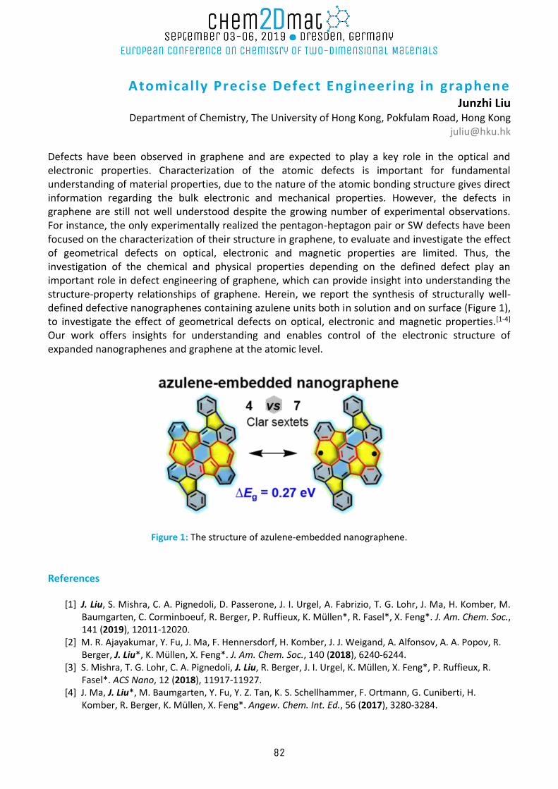
Atomical ly Precise Defect Engineering in graphene
Junzhi Liu Department of Chemistry, The University of Hong Kong, Pokfulam Road, Hong Kong
Defects have been observed in graphene and are expected to play a key role in the optical and electronic properties. Characterization of the atomic defects is important for fundamental understanding of material properties, due to the nature of the atomic bonding structure gives direct information regarding the bulk electronic and mechanical properties. However, the defects in graphene are still not well understood despite the growing number of experimental observations. For instance, the only experimentally realized the pentagon-heptagon pair or SW defects have been focused on the characterization of their structure in graphene, to evaluate and investigate the effect of geometrical defects on optical, electronic and magnetic properties are limited. Thus, the investigation of the chemical and physical properties depending on the defined defect play an important role in defect engineering of graphene, which can provide insight into understanding the structure-property relationships of graphene. Herein, we report the synthesis of structurally well-defined defective nanographenes containing azulene units both in solution and on surface (Figure 1), to investigate the effect of geometrical defects on optical, electronic and magnetic properties.[1-4]
Our work offers insights for understanding and enables control of the electronic structure of expanded nanographenes and graphene at the atomic level.
Figure 1: The structure of azulene-embedded nanographene.
References
[1] J. Liu, S. Mishra, C. A. Pignedoli, D. Passerone, J. I. Urgel, A. Fabrizio, T. G. Lohr, J. Ma, H. Komber, M. Baumgarten, C. Corminboeuf, R. Berger, P. Ruffieux, K. Müllen*, R. Fasel*, X. Feng*. J. Am. Chem. Soc., 141 (2019), 12011-12020.
[2] M. R. Ajayakumar, Y. Fu, J. Ma, F. Hennersdorf, H. Komber, J. J. Weigand, A. Alfonsov, A. A. Popov, R. Berger, J. Liu*, K. Müllen, X. Feng*. J. Am. Chem. Soc., 140 (2018), 6240-6244.
[3] S. Mishra, T. G. Lohr, C. A. Pignedoli, J. Liu, R. Berger, J. I. Urgel, K. Müllen, X. Feng*, P. Ruffieux, R. Fasel*. ACS Nano, 12 (2018), 11917-11927.
[4] J. Ma, J. Liu*, M. Baumgarten, Y. Fu, Y. Z. Tan, K. S. Schellhammer, F. Ortmann, G. Cuniberti, H. Komber, R. Berger, K. Müllen, X. Feng*. Angew. Chem. Int. Ed., 56 (2017), 3280-3284.
82
Synthesis of ultrathin nanoporous carbon membrane for eff ic ient energy harvesting from sal inity gradient
Xue Liu1, Meng He1, Haoyuan Qi2, Ute Kaiser2 and Grégory F. Schneider1 1. Leiden Institute of Chemistry, Faculty of Science, Leiden University, 2333 CC Leiden, The
Netherlands 2. Central Facility of Electron Microscopy, Microscopy Group of Materials Science, Ulm
University, 89081 Ulm, Germany Organization, Address, City, Country [email protected]
Full-carbon materials have developed rapidly in the past two decades. Among them, nanoporous graphene has recently attracted great attention owing to its potential application for bio-molecules sequencing (1), ion transport (2), gas separation (3), water purification (4) and energy generation (5). However, the synthesis of atomically thin nanoporous membranes with nanopores diameters as low as subnanometers still represents an enormous challenge if large scale membranes are concerned (typically area bigger than square millimeters). Here we report a bottom-up approach to synthesize nanoporous ultrathin carbon membrane comprising pores of 3.6 ± 1.8 nm from polycyclic aromatic hydrocarbons. The ionic conductance measurements reveal that the membrane is cation selective. The membrane can efficiently convert the salinity gradient energy into electricity, with an energy conversion efficiency of 40 % and output power density of 67 W/m2. The atomically thin porous polycyclic aromatic hydrocarbon membranes we introduce therefore represent new scaffolds that will add to the rapid developing fields of sustainable energy and membrane technology. References
[1] H. Arjmandi-Tash, L. A. Belyaeva and G. F. Schneider, Chem. Soc. Rev., 2016, 45, 476-493. [2] R. C. Rollings, A. T. Kuan and J. A. Golovchenko, Nat. Commun., 2016, 7, 11408. [3] D.E. Jiang, V. R. Cooper and S. Dai, Nano Lett., 2009, 9, 4019-4024. [4] E. N. Wang and R. Karnik, Nat Nano, 2012, 7, 552-554. [5] J. D. Feng, M. Graf, K. Liu, D. Ovchinnikov, D. Dumcenco, M. Heiranian, V. Nandigana, N. R. Aluru, A.
Kis and A. Radenovic, Nature, 2016, 536, 197-200.
83
Covalent Functionalization of Surface -Supported Graphene and MoS2: Chemical versus Electrochemical Routes
Kunal S. Mali, Steven De Feyter KU Leuven, Department of Chemistry, Division of Molecular Imaging and Photonics, Leuven,
Belgium-3001 [email protected]
Two-dimensional (2D) materials which consist of atomically thin sheets of materials arrived on the scene in early 2000s with the successful isolation of graphene. Graphene is a single atom thick sheet of sp2-hybridized carbon bonded in a honeycomb lattice. It has exceptional electronic, optical, mechanical and thermal properties that outperform those of most of the existing materials. The research on graphene further prompted emergence of related layered materials such as black phosphorous, silicene, germanene and transition metal dichalcogenides (TMDs) such as MoS2. Due to their exotic properties, these materials offer virtually endless opportunities for fundamental research as well as cutting edge applications.[1]
Most of these layered materials however exist as single layers only when supported by another solid surface or when stabilized by physisorbed or chemisorbed organic molecules. Given their layered nature, most layered materials are extremely difficult to disperse in typical solvents. Covalent attachment of organic molecules onto their basal plane allows dispersion of these materials in (organic) solvents thereby improving their processability. Such dispersions can be used in composite materials and as functional inks. Moreover, covalent functionalization allows modification of the intrinsic electrical, electronic and optical properties of these 2D materials.[2]
In this contribution, I will discuss covalent modification graphene, graphite and MoS2 using diazonium chemistry. Two different routes for reductive decomposition of diazonium salts namely, chemical and electrochemical, will be discussed in detail. Special focus is on sub-nanometer characterization of modified materials using scanning tunneling and atomic force microscopy (STM and AFM). The use of covalently modified graphene surfaces as seed layers for atomic layer deposition (ALD) will also be discussed briefly.
References [1] R. Mas-Balleste, C. Gomez-Navarro, J. Gomez-Herrero and F. Zamora, Nanoscale 2011, 3, 20-30. [2] M. Gobbi, E. Orgiu and P. Samorì, Adv. Mater. 0, 1706103.
84
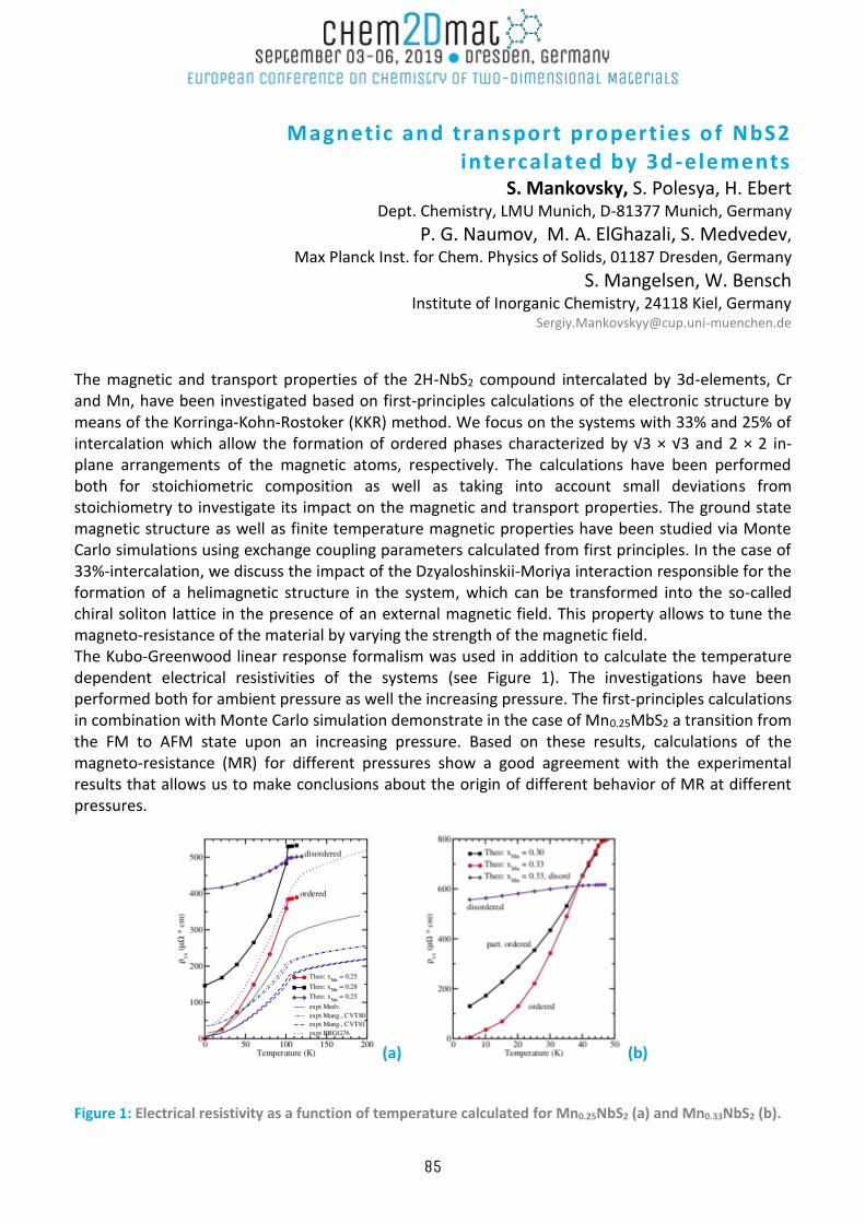
Magnetic and transport propert ies of NbS2 intercalated by 3d -elements
S. Mankovsky, S. Polesya, H. Ebert Dept. Chemistry, LMU Munich, D-81377 Munich, Germany
P. G. Naumov, M. A. ElGhazali, S. Medvedev,
Max Planck Inst. for Chem. Physics of Solids, 01187 Dresden, Germany
S. Mangelsen, W. Bensch Institute of Inorganic Chemistry, 24118 Kiel, Germany
The magnetic and transport properties of the 2H-NbS2 compound intercalated by 3d-elements, Cr and Mn, have been investigated based on first-principles calculations of the electronic structure by means of the Korringa-Kohn-Rostoker (KKR) method. We focus on the systems with 33% and 25% of intercalation which allow the formation of ordered phases characterized by √3 × √3 and 2 × 2 in-plane arrangements of the magnetic atoms, respectively. The calculations have been performed both for stoichiometric composition as well as taking into account small deviations from stoichiometry to investigate its impact on the magnetic and transport properties. The ground state magnetic structure as well as finite temperature magnetic properties have been studied via Monte Carlo simulations using exchange coupling parameters calculated from first principles. In the case of 33%-intercalation, we discuss the impact of the Dzyaloshinskii-Moriya interaction responsible for the formation of a helimagnetic structure in the system, which can be transformed into the so-called chiral soliton lattice in the presence of an external magnetic field. This property allows to tune the magneto-resistance of the material by varying the strength of the magnetic field. The Kubo-Greenwood linear response formalism was used in addition to calculate the temperature dependent electrical resistivities of the systems (see Figure 1). The investigations have been performed both for ambient pressure as well the increasing pressure. The first-principles calculations in combination with Monte Carlo simulation demonstrate in the case of Mn0.25MbS2 a transition from the FM to AFM state upon an increasing pressure. Based on these results, calculations of the magneto-resistance (MR) for different pressures show a good agreement with the experimental results that allows us to make conclusions about the origin of different behavior of MR at different pressures.
(a) (b) Figure 1: Electrical resistivity as a function of temperature calculated for Mn0.25NbS2 (a) and Mn0.33NbS2 (b).
85
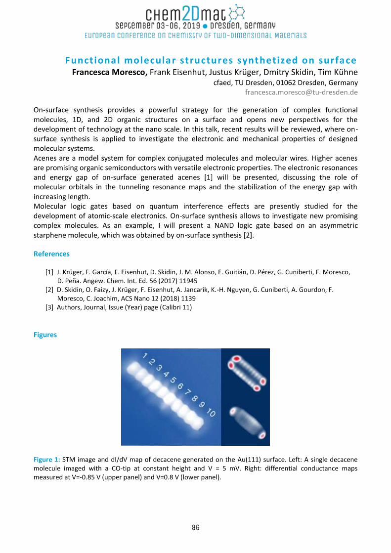
Functional molecular structures synthetized on surface Francesca Moresco, Frank Eisenhut, Justus Krüger, Dmitry Skidin, Tim Kühne
cfaed, TU Dresden, 01062 Dresden, Germany [email protected]
On-surface synthesis provides a powerful strategy for the generation of complex functional molecules, 1D, and 2D organic structures on a surface and opens new perspectives for the development of technology at the nano scale. In this talk, recent results will be reviewed, where on-surface synthesis is applied to investigate the electronic and mechanical properties of designed molecular systems. Acenes are a model system for complex conjugated molecules and molecular wires. Higher acenes are promising organic semiconductors with versatile electronic properties. The electronic resonances and energy gap of on-surface generated acenes [1] will be presented, discussing the role of molecular orbitals in the tunneling resonance maps and the stabilization of the energy gap with increasing length. Molecular logic gates based on quantum interference effects are presently studied for the development of atomic-scale electronics. On-surface synthesis allows to investigate new promising complex molecules. As an example, I will present a NAND logic gate based on an asymmetric starphene molecule, which was obtained by on-surface synthesis [2]. References
[1] J. Krüger, F. García, F. Eisenhut, D. Skidin, J. M. Alonso, E. Guitián, D. Pérez, G. Cuniberti, F. Moresco, D. Peña. Angew. Chem. Int. Ed. 56 (2017) 11945
[2] D. Skidin, O. Faizy, J. Krüger, F. Eisenhut, A. Jancarik, K.-H. Nguyen, G. Cuniberti, A. Gourdon, F. Moresco, C. Joachim, ACS Nano 12 (2018) 1139
[3] Authors, Journal, Issue (Year) page (Calibri 11)
Figures
Figure 1: STM image and dI/dV map of decacene generated on the Au(111) surface. Left: A single decacene molecule imaged with a CO-tip at constant height and V = 5 mV. Right: differential conductance maps measured at V=-0.85 V (upper panel) and V=0.8 V (lower panel).
86
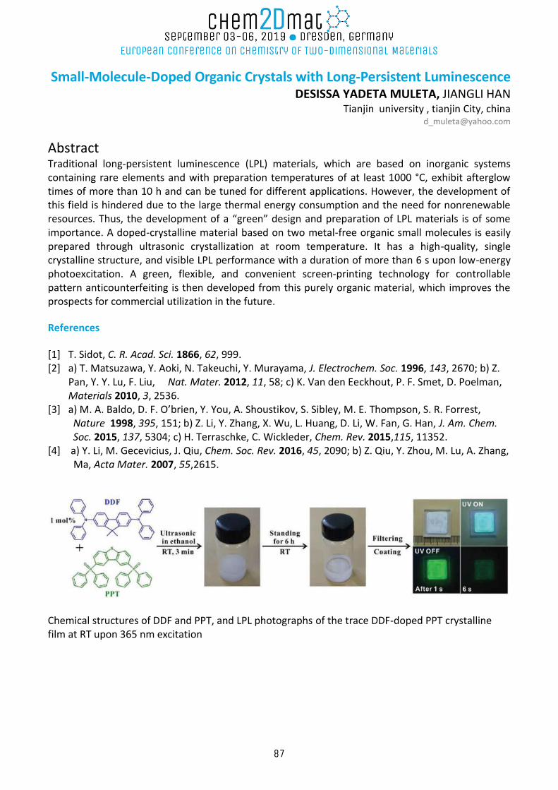
Small-Molecule-Doped Organic Crystals with Long-Persistent Luminescence DESISSA YADETA MULETA, JIANGLI HAN
Tianjin university , tianjin City, china [email protected]
Abstract Traditional long-persistent luminescence (LPL) materials, which are based on inorganic systems containing rare elements and with preparation temperatures of at least 1000 °C, exhibit afterglow times of more than 10 h and can be tuned for different applications. However, the development of this field is hindered due to the large thermal energy consumption and the need for nonrenewable resources. Thus, the development of a “green” design and preparation of LPL materials is of some importance. A doped-crystalline material based on two metal-free organic small molecules is easily prepared through ultrasonic crystallization at room temperature. It has a high-quality, single crystalline structure, and visible LPL performance with a duration of more than 6 s upon low-energy photoexcitation. A green, flexible, and convenient screen-printing technology for controllable pattern anticounterfeiting is then developed from this purely organic material, which improves the prospects for commercial utilization in the future.
References [1] T. Sidot, C. R. Acad. Sci. 1866, 62, 999. [2] a) T. Matsuzawa, Y. Aoki, N. Takeuchi, Y. Murayama, J. Electrochem. Soc. 1996, 143, 2670; b) Z. Pan, Y. Y. Lu, F. Liu, Nat. Mater. 2012, 11, 58; c) K. Van den Eeckhout, P. F. Smet, D. Poelman, Materials 2010, 3, 2536. [3] a) M. A. Baldo, D. F. O’brien, Y. You, A. Shoustikov, S. Sibley, M. E. Thompson, S. R. Forrest,
Nature 1998, 395, 151; b) Z. Li, Y. Zhang, X. Wu, L. Huang, D. Li, W. Fan, G. Han, J. Am. Chem. Soc. 2015, 137, 5304; c) H. Terraschke, C. Wickleder, Chem. Rev. 2015,115, 11352.
[4] a) Y. Li, M. Gecevicius, J. Qiu, Chem. Soc. Rev. 2016, 45, 2090; b) Z. Qiu, Y. Zhou, M. Lu, A. Zhang, Ma, Acta Mater. 2007, 55,2615.
Chemical structures of DDF and PPT, and LPL photographs of the trace DDF-doped PPT crystalline film at RT upon 365 nm excitation
87

Production of 2D nanocarbons through chemical , e lectrochemical , or mechanical methodologies
Yuta Nishina, Campeon Benoit, Ryuji Takata Okayama University, 3-1-1 Tsushimanaka, Okayama, Japan
Exfoliation of graphite through oxidation is a promising technique to produce two-dimensional nanocarbons especially graphene oxide (GO) on a large scale. We have achieved a 500 g scale production of GO in laboratory, and 10 kg production in prototype plant by optimized Hummers’ method using KMnO4 in H2SO4. These large-scale productions were achieved by mechanistic study of the oxidation process using in situ analyses, such as XRD and XANES analyses. Our optimized GO production processes enabled the control of the size, oxidation degree, and functional group distribution on GO [1]. However, the conventional oxidation of graphite uses a strong oxidant in concentrated sulfuric acid; thus, there are environmental and safety issues. In contrast, the electrochemical oxidation of a graphite electrode has recently attracted considerable attention because it does not require oxidants or sulfuric acid. GO produced through the existing electrochemical method is generally lacking in quality, due to the non-uniform destruction of the intermediately oxidized graphite. We developed a method for the non-destructive oxidation of graphite using specially designed electrolyte. It is confirmed that the choice of solvents and electrochemical conditions enabled fine control over the functionalization degree and type of functional groups on GO. Compared to chemically generated GO, the electrochemically generated GO exhibits similar or better physical and chemical properties toward lithium ion battery electrodes and water purification membranes. This electrochemical method is also applicable to a continuous flow system, thus promising the mass production of GO for future industrialization. Further, direct exfoliation of graphite in liquid was also achieved without oxidation.
References [1] N. Morimoto, Y. Nishina, et al, Chem. Mater, 46 (2017), 4160–4165.
Figures
Figure 1: Methods for the production of 2D nanocarbons.
88
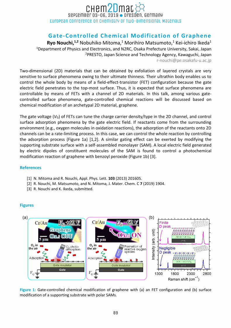
Gate-Control led Chemical Modification of Graphene Ryo Nouchi,1,2 Nobuhiko Mitoma,1 Morihiro Matsumoto,1 Kei-ichiro Ikeda1
1Department of Physics and Electronics, and N2RC, Osaka Prefecture University, Sakai, Japan 2PRESTO, Japan Science and Technology Agency, Kawaguchi, Japan
Two-dimensional (2D) materials that can be obtained by exfoliation of layered crystals are very sensitive to surface phenomena owing to their ultimate thinness. Their ultrathin body enables us to control the whole body by means of a field-effect-transistor (FET) configuration because the gate electric field penetrates to the top-most surface. Thus, it is expected that surface phenomena are controllable by means of FETs with a channel of 2D materials. In this talk, among various gate-controlled surface phenomena, gate-controlled chemical reactions will be discussed based on chemical modification of an archetypal 2D material, graphene. The gate voltage (VG) of FETs can tune the charge carrier density/type in the 2D channel, and control surface adsorption phenomena by the gate electric field. If reactants come from the surrounding environment (e.g., oxygen molecules in oxidation reactions), the adsorption of the reactants onto 2D channels can be a rate-limiting process. In this case, we can control the whole reaction by controlling the adsorption process (Figure 1a) [1,2]. A similar gating effect can be exerted by modifying the supporting substrate surface with a self-assembled monolayer (SAM). A local electric field generated by electric dipoles of constituent molecules of the SAM is found to control a photochemical modification reaction of graphene with benzoyl peroxide (Figure 1b) [3]. References
[1] N. Mitoma and R. Nouchi, Appl. Phys. Lett. 103 (2013) 201605. [2] R. Nouchi, M. Matsumoto, and N. Mitoma, J. Mater. Chem. C 7 (2019) 1904. [3] R. Nouchi and K. Ikeda, submitted.
Figures
Figure 1: Gate-controlled chemical modification of graphene with (a) an FET configuration and (b) surface modification of a supporting substrate with polar SAMs.
89
Chemistry of F luorographene, From Understanding to Applications
Michal Otyepka, Aristides Bakandritsos, Hugo Barès, Piotr Blonski, Demetrios D. Chronopoulos, Petr Jakubec, Petr Lazar, Miroslav Medveď, Martin Pykal, Eleni
Vermisoglou, Jiří Tuček, Radek Zbořil Regional Centre of Advanced Technologies and Materials & Department of Physical Chemistry,
Faculty of Science, Palacký University Olomouc, 17. listopadu 12, 771 46 Olomouc, Czech Republic [email protected]
Fluorographene (FG) is a stoichiometric graphene derivative with C1F1 composition. It can be prepared by delamination of graphite fluoride, which is an industrially available material. As a perfluorinated hydrocarbon, fluorographene was considered unreactive, but in reality, it undergoes various chemical reactions at rather mild conditions [1]. Fluorographene and fluorinated graphenes (CFx) are susceptible for reductive defluorination, nucleophilic attack, Grignard [2], Bingel-Hirsch [3], photo Diels-Alder [4] and Sonogashira [5] reactions. The reactions result in homogeneously and densely functionalized graphenes. These findings make fluorographene a well-suited material for large scale synthesis of a wide spectrum of graphene derivatives. Such materials can be utilized in a broad spectrum of applications. Due to high-conductivity and water dispersibility some of them can be used as electrode materials for supercapacitors [3, 6]. Various hydroxyfluorographenes can bear room-temperature antiferromagnetic or ferromagnetic ordering based on their composition [7]. Cyanographene, and graphene acid [8] are well biocompatible materials suitable for further functionalization. Conjugating these materials with redox active centers, e.g., ferrocene, can lead to heterogenous catalysts [9]. Anchoring metal ions to cyanographene resulted in a single-atom catalyst very active in oxidative amine coupling reactions [10]. ERC Consolidator grant (H2020, ID: 683024) 2D-Chem is gratefully acknowledged. References [1] Zboril R. et al., Small, 6 (2010) 2885; Dubecky M. et al., J. Phys. Chem. Lett., 6 (2015) 1430; Medveď M. et al., Nanoscale (2018), 4696; Chronopoulos D. et al., Appl. Mat. Today 9 (2017) 60. [2] Chronopoulos D. et al., Chem. Mater 29 (2017) 926. [3] Bakandritsos A. et al., Adv. Funct. Mater 28 (2018) 1801111. [4] Bares H. et al., Carbon 145 (2019) 251. [5] Chronopoulos D. et al., ChemComm 55 (2019) 1088. [6] Bakandritsos A. et al., FlatChem 13 (2019) 25. [7] Tuček J. et al., Nat. Commun. 8 (2017) 14525; Tuček J. et al., ACS Nano 12 (2018), 12847. [8] Bakandritsos A. et al., ACS Nano 11 (2017) 2982. [9] Mosconi D. et al., Carbon 143 (2019) 318. [10] Bakandritsos A. et al., Adv. Mater. (2019) in press (https://doi.org/10.1002/adma.201900323).
90
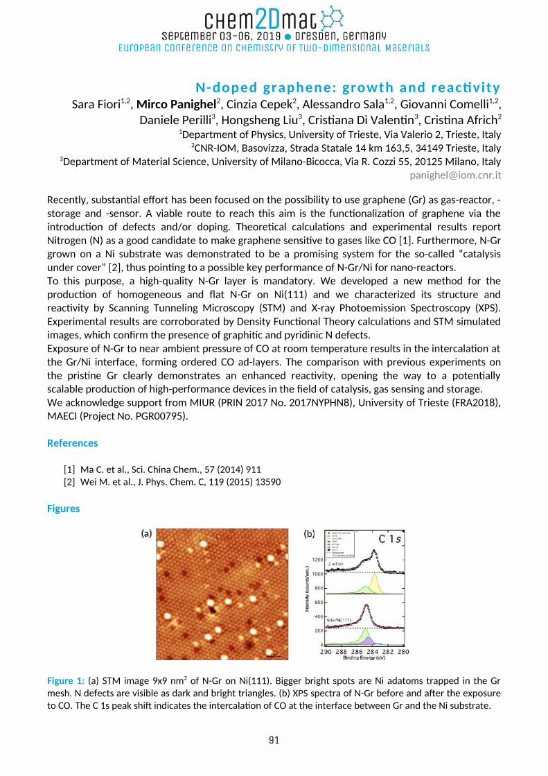
N-doped graphene: growth and reactivitySara Fiori1,2, Mirco Panighel2, Cinzia Cepek2, Alessandro Sala1,2, Giovanni Comelli1,2,
Daniele Perilli3, Hongsheng Liu3, Cristiana Di Valentin3, Cristina Africh2
1Department of Physics, University of Trieste, Via Valerio 2, Trieste, Italy2CNR-IOM, Basovizza, Strada Statale 14 km 163,5, 34149 Trieste, Italy
3Department of Material Science, University of Milano-Bicocca, Via R. Cozzi 55, 20125 Milano, [email protected]
Recently, substantial effort has been focused on the possibility to use graphene (Gr) as gas-reactor, -storage and -sensor. A viable route to reach this aim is the functionalization of graphene via the introduction of defects and/or doping. Theoretical calculations and experimental results report Nitrogen (N) as a good candidate to make graphene sensitive to gases like CO [1]. Furthermore, N-Gr grown on a Ni substrate was demonstrated to be a promising system for the so-called “catalysis under cover” [2], thus pointing to a possible key performance of N-Gr/Ni for nano-reactors.To this purpose, a high-quality N-Gr layer is mandatory. We developed a new method for the production of homogeneous and flat N-Gr on Ni(111) and we characterized its structure and reactivity by Scanning Tunneling Microscopy (STM) and X-ray Photoemission Spectroscopy (XPS). Experimental results are corroborated by Density Functional Theory calculations and STM simulated images, which confirm the presence of graphitic and pyridinic N defects.Exposure of N-Gr to near ambient pressure of CO at room temperature results in the intercalation at the Gr/Ni interface, forming ordered CO ad-layers. The comparison with previous experiments on the pristine Gr clearly demonstrates an enhanced reactivity, opening the way to a potentially scalable production of high-performance devices in the field of catalysis, gas sensing and storage.We acknowledge support from MIUR (PRIN 2017 No. 2017NYPHN8), University of Trieste (FRA2018), MAECI (Project No. PGR00795).
References
[1] Ma C. et al., Sci. China Chem., 57 (2014) 911[2] Wei M. et al., J. Phys. Chem. C, 119 (2015) 13590
Figures
Figure 1: (a) STM image 9x9 nm2 of N-Gr on Ni(111). Bigger bright spots are Ni adatoms trapped in the Gr mesh. N defects are visible as dark and bright triangles. (b) XPS spectra of N-Gr before and after the exposure to CO. The C 1s peak shift indicates the intercalation of CO at the interface between Gr and the Ni substrate.
91
New tools for the chemical modification of 2D materials Emilio M. Pérez
C/Faraday 9, Ciudad Universitaria de Canto Blanco, E28049 Madrid, Spain [email protected]
The extraordinary properties of graphene and transition metal dichalcogenides (TMDCs) can be further improved/tuned by decoration with adequate molecular entities. [1] However, the chemistry of 2D materials remains quite a challenge, in particular due to the typically low reactivity -that makes them stable- and the large number of identical atoms -which hinders selective functionalization.
In this presentation, we will describe a method to functionalize graphene covalently with exquisite (>97%) atomic selectivity and yield (92%). The periodic landscape is provided by a single monolayer of graphene grown on Ru(0001) that presents a moiré pattern due to the mismatch between the carbon and ruthenium hexagonal lattices. The moiré contains periodically arranged areas where the graphene–ruthenium interaction is enhanced and shows higher chemical reactivity.[2] Furthermore, we will show how this type of functionalized graphene acts as a catalyst for an unusual and reversible C-C bond forming reaction.[3]
With regards to TMDCs, we will describe improved methods for their production through liquid-phase exfoliation (LPE),[4] and describe strategies for their noncovalent[5] and covalent[6] functionalisation. The covalent functionalisation is very mild (room temperature) and exploits the inherent soft-nucleophilicity of sulfur to functionalize MoS2 and WS2 with the prototypical electrophilic counterpart of S: maleimides. Finally, we will report simple strategies to construct functioning electronic devices from colloidal suspensions of 2D materials obtained by LPE.[7]
References
[1] S. Bertolazzi, M. Gobbi, Y. Zhao, P. Samori, C. Backes, Chem. Soc. Rev. 2018, 47, 6845-6888. [2] a) J. J. Navarro, S. Leret, F. Calleja, D. Stradi, A. Black, R. Bernardo-Gavito, M. Garnica, D. Granados, A.
L. Vazquez de Parga, E. M. Pérez, R. Miranda, Nano Lett. 2016, 16, 355-361; b) J. J. Navarro, F. Calleja, R. Miranda, E. M. Pérez, A. L. V. d. Parga, Chem. Commun. 2017, 53, 10418-10421.
[3] J. J. Navarro, M. Pisarra, B. Nieto-Ortega, J. Villalva, C. G. Ayani, C. Díaz, F. Calleja, R. Miranda, F. Martín, E. M. Pérez, A. L. Vázquez de Parga, Science Adv. 2018, 4, eaau9366.
[4] M. M. Bernal, L. Alvarez, E. Giovanelli, A. Arnaiz, L. Ruiz-Gonzalez, S. Casado, D. Granados, A. M. Pizarro, A. Castellanos-Gomez, E. M. Pérez, 2D Mater. 2016, 3, 035014/035011
[5] A. J. Molina-Mendoza, L. Vaquero-Garzon, S. Leret, L. d. Juan-Fernández, E. M. Pérez, A. Castellanos-Gomez, Chem. Commun. 2016, 52, 14365-14368.
[6] M. Vera-Hidalgo, E. Giovanelli, C. Navio, E. M. Pérez, J. Am. Chem. Soc. 2019, 141, 3767-3771. [7] E. Burzuri, M. Vera-Hidalgo, E. Giovanelli, J. Villalva, A. Castellanos-Gomez, E. M. Pérez, Nanoscale
2018, 10, 7966-7970.
92
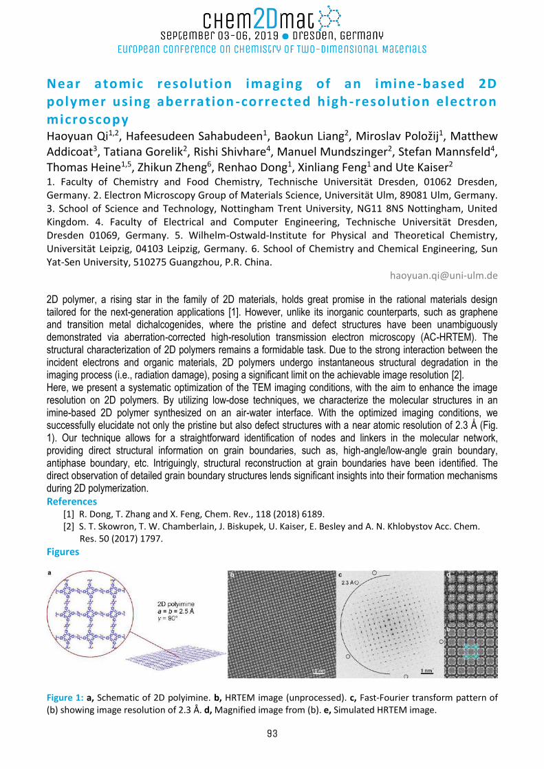
Near atomic resolution imaging of an imine -based 2D polymer using aberration -corrected high-resolution electron microscopy Haoyuan Qi1,2, Hafeesudeen Sahabudeen1, Baokun Liang2, Miroslav Položij1, Matthew Addicoat3, Tatiana Gorelik2, Rishi Shivhare4, Manuel Mundszinger2, Stefan Mannsfeld4, Thomas Heine1,5, Zhikun Zheng6, Renhao Dong1, Xinliang Feng1 and Ute Kaiser2 1. Faculty of Chemistry and Food Chemistry, Technische Universität Dresden, 01062 Dresden, Germany. 2. Electron Microscopy Group of Materials Science, Universität Ulm, 89081 Ulm, Germany. 3. School of Science and Technology, Nottingham Trent University, NG11 8NS Nottingham, United Kingdom. 4. Faculty of Electrical and Computer Engineering, Technische Universität Dresden, Dresden 01069, Germany. 5. Wilhelm-Ostwald-Institute for Physical and Theoretical Chemistry, Universität Leipzig, 04103 Leipzig, Germany. 6. School of Chemistry and Chemical Engineering, Sun Yat-Sen University, 510275 Guangzhou, P.R. China.
[email protected] 2D polymer, a rising star in the family of 2D materials, holds great promise in the rational materials design tailored for the next-generation applications [1]. However, unlike its inorganic counterparts, such as graphene and transition metal dichalcogenides, where the pristine and defect structures have been unambiguously demonstrated via aberration-corrected high-resolution transmission electron microscopy (AC-HRTEM). The structural characterization of 2D polymers remains a formidable task. Due to the strong interaction between the incident electrons and organic materials, 2D polymers undergo instantaneous structural degradation in the imaging process (i.e., radiation damage), posing a significant limit on the achievable image resolution [2]. Here, we present a systematic optimization of the TEM imaging conditions, with the aim to enhance the image resolution on 2D polymers. By utilizing low-dose techniques, we characterize the molecular structures in an imine-based 2D polymer synthesized on an air-water interface. With the optimized imaging conditions, we successfully elucidate not only the pristine but also defect structures with a near atomic resolution of 2.3 Å (Fig. 1). Our technique allows for a straightforward identification of nodes and linkers in the molecular network, providing direct structural information on grain boundaries, such as, high-angle/low-angle grain boundary, antiphase boundary, etc. Intriguingly, structural reconstruction at grain boundaries have been identified. The direct observation of detailed grain boundary structures lends significant insights into their formation mechanisms during 2D polymerization.
References [1] R. Dong, T. Zhang and X. Feng, Chem. Rev., 118 (2018) 6189. [2] S. T. Skowron, T. W. Chamberlain, J. Biskupek, U. Kaiser, E. Besley and A. N. Khlobystov Acc. Chem.
Res. 50 (2017) 1797. Figures
Figure 1: a, Schematic of 2D polyimine. b, HRTEM image (unprocessed). c, Fast-Fourier transform pattern of (b) showing image resolution of 2.3 Å. d, Magnified image from (b). e, Simulated HRTEM image.
93
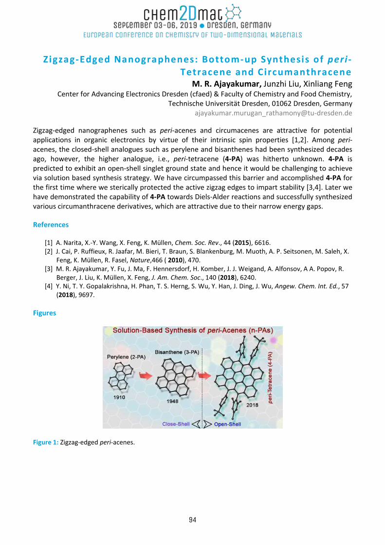
Zigzag-Edged Nanographenes: Bottom-up Synthesis of peri -Tetracene and Circumanthracene
M. R. Ajayakumar, Junzhi Liu, Xinliang Feng Center for Advancing Electronics Dresden (cfaed) & Faculty of Chemistry and Food Chemistry,
Technische Universitat Dresden, 01062 Dresden, Germany [email protected]
Zigzag-edged nanographenes such as peri-acenes and circumacenes are attractive for potential applications in organic electronics by virtue of their intrinsic spin properties [1,2]. Among peri-acenes, the closed-shell analogues such as perylene and bisanthenes had been synthesized decades ago, however, the higher analogue, i.e., peri-tetracene (4-PA) was hitherto unknown. 4-PA is predicted to exhibit an open‐shell singlet ground state and hence it would be challenging to achieve via solution based synthesis strategy. We have circumpassed this barrier and accomplished 4-PA for the first time where we sterically protected the active zigzag edges to impart stability [3,4]. Later we have demonstrated the capability of 4-PA towards Diels-Alder reactions and successfully synthesized various circumanthracene derivatives, which are attractive due to their narrow energy gaps.
References
[1] A. Narita, X.-Y. Wang, X. Feng, K. Müllen, Chem. Soc. Rev., 44 (2015), 6616. [2] J. Cai, P. Ruffieux, R. Jaafar, M. Bieri, T. Braun, S. Blankenburg, M. Muoth, A. P. Seitsonen, M. Saleh, X.
Feng, K. Müllen, R. Fasel, Nature,466 ( 2010), 470. [3] M. R. Ajayakumar, Y. Fu, J. Ma, F. Hennersdorf, H. Komber, J. J. Weigand, A. Alfonsov, A A. Popov, R.
Berger, J. Liu, K. Müllen, X. Feng, J. Am. Chem. Soc., 140 (2018), 6240. [4] Y. Ni, T. Y. Gopalakrishna, H. Phan, T. S. Herng, S. Wu, Y. Han, J. Ding, J. Wu, Angew. Chem. Int. Ed., 57
(2018), 9697.
Figures
Figure 1: Zigzag-edged peri-acenes.
94
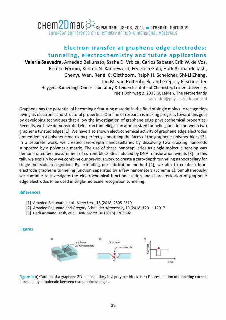
Electron transfer at graphene edge electrodes:
tunneling , electrochemistry and future applicat ions
Valeria Saavedra, Amedeo Bellunato, Sasha D. Vrbica, Carlos Sabater, Erik W. de Vos, Remko Fermin, Kirsten N. Kanneworff, Federica Galli, Hadi Arjmandi-Tash,
Chenyu Wen, René C. Olsthoorn, Ralph H. Scheicher, Shi-Li Zhang, Jan M. van Ruitenbeek, and Grégory F. Schneider
Huygens-Kamerlingh Onnes Laboratory & Leiden Institute of Chemistry, Leiden University, Niels Bohrweg 2, 2333CA Leiden, The Netherlands
Graphene has the potential of becoming a featuring material in the field of single molecule recognition owing its electronic and structural properties. Our line of research is making progress toward this goal by developing techniques that allow the investigation of graphene edge physicochemical properties. Recently, we have demonstrated electron tunneling in an atomic-sized tunneling junction between two graphene twisted edges [1]. We have also shown electrochemical activity of graphene edge electrodes embedded in a polymeric matrix by perfectly smoothing the faces of the graphene-polymer block [2]. In a separate work, we created zero-depth nanocapillaries by dissolving two crossing nanorods supported by a polymeric matrix. The use of these nanocapillaries as single-molecule sensing was demonstrated by measurement of current blockades induced by DNA translocation events [3]. In this talk, we explain how we combine our previous work to create a zero-depth tunneling nanocapillary for single-molecule recognition. By extending our fabrication method [2], we aim to create a four-electrode graphene tunneling junction separated by a few nanometers (Scheme 1). Simultaneously, we continue to investigate the electrochemical functionalization and characterization of graphene edge electrodes to be used in single-molecule recognition tunneling.
References
[1] Amedeo Bellunato, et al. Nano Lett., 18 (2018) 2505-2510 [2] Amadeo Bellunato and Grégory Schneider. Nanoscale, 10 (2018) 12011-12017 [3] Hadi Arjmandi-Tash, et al. Adv. Mater. 30 (2018) 1703602
Figures
Figure 1: a) Cartoon of a graphene 2D-nanocapillary in a polymer block. b-c) Representation of tunneling current
blockade by a molecule between two graphene edges.
95
Mimic 1D propert ies on continuous 2D materia ls: the pi lot case of graphene on NiC x /Ni(100)
A. Sala12, V. Carnevali1, Z. Zou2, M. Panighel2, F. Genuzio3, T. O. Menteş3, A. Locatelli3, C. Cepek2, M. Peressi1, C. Africh2, G. Comelli12
(1) Department of Physics, University of Trieste, via Valerio 2, 34127 Trieste, Italy (2) IOM-CNR, S.S. 14 km 163.5 in AREA Science Park, 34149 Trieste, Italy
(3) Elettra Sincrotrone Trieste, S.S. 14 km 163.5 in AREA Science Park, 34149 Trieste, Italy [email protected]
Tailoring electronic properties on 2D materials by inducing 1D electronic states via lateral confinement is a well-established research route, with real applications almost exclusively on graphene due to the difficulty of bottom-up synthesis of nanoribbon made of other 2D materials. Here we present a different approach, based on smart choice of the substrate, that allows the creation of 1D stripes embedded on a continuous 2D material, namely graphene grown on Ni(100)[1]. Such stripes are forced to have different electronic properties by the selective formation at the graphene/metal interface of nickel carbide that decouples graphene from the substrate only at selected lanes of 1D moiré. Our results, obtained with combination of microscopy, spectroscopy and diffraction techniques and corroborated by DFT calculations, show that such 1D stripes have electronic properties that resemble the ones of zig-zag graphene nanoribbons, and that this procedure offers the unprecedented possibility to measure the band structure of 2D materials with 1D states by angle-resolved photoelectron spectroscopy. This approach can in principle be extended to other 2D materials, giving access to characterization of low-dimensional states without passing through bottom-up synthesis of nanoribbons.
References
[1] Z. Zou et al., Carbon 130 (2018) 441-447
96
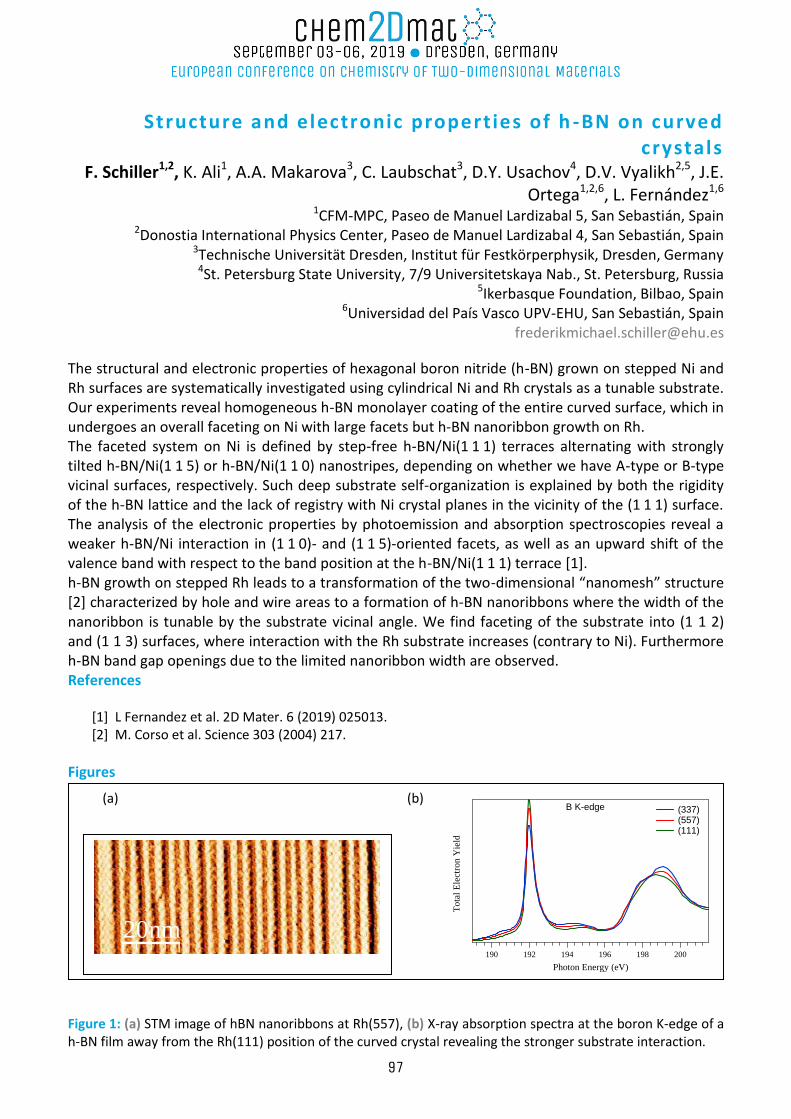
Structure and electronic propert ies of h -BN on curved crystals
F. Schiller1,2, K. Ali1, A.A. Makarova3, C. Laubschat3, D.Y. Usachov4, D.V. Vyalikh2,5, J.E. Ortega1,2,6, L. Fernández1,6
1CFM-MPC, Paseo de Manuel Lardizabal 5, San Sebastián, Spain 2Donostia International Physics Center, Paseo de Manuel Lardizabal 4, San Sebastián, Spain
3Technische Universität Dresden, Institut für Festkörperphysik, Dresden, Germany 4St. Petersburg State University, 7/9 Universitetskaya Nab., St. Petersburg, Russia
5Ikerbasque Foundation, Bilbao, Spain 6Universidad del País Vasco UPV-EHU, San Sebastián, Spain
The structural and electronic properties of hexagonal boron nitride (h-BN) grown on stepped Ni and Rh surfaces are systematically investigated using cylindrical Ni and Rh crystals as a tunable substrate. Our experiments reveal homogeneous h-BN monolayer coating of the entire curved surface, which in undergoes an overall faceting on Ni with large facets but h-BN nanoribbon growth on Rh. The faceted system on Ni is defined by step-free h-BN/Ni(1 1 1) terraces alternating with strongly tilted h-BN/Ni(1 1 5) or h-BN/Ni(1 1 0) nanostripes, depending on whether we have A-type or B-type vicinal surfaces, respectively. Such deep substrate self-organization is explained by both the rigidity of the h-BN lattice and the lack of registry with Ni crystal planes in the vicinity of the (1 1 1) surface. The analysis of the electronic properties by photoemission and absorption spectroscopies reveal a weaker h-BN/Ni interaction in (1 1 0)- and (1 1 5)-oriented facets, as well as an upward shift of the valence band with respect to the band position at the h-BN/Ni(1 1 1) terrace [1]. h-BN growth on stepped Rh leads to a transformation of the two-dimensional “nanomesh” structure [2] characterized by hole and wire areas to a formation of h-BN nanoribbons where the width of the nanoribbon is tunable by the substrate vicinal angle. We find faceting of the substrate into (1 1 2) and (1 1 3) surfaces, where interaction with the Rh substrate increases (contrary to Ni). Furthermore h-BN band gap openings due to the limited nanoribbon width are observed. References
[1] L Fernandez et al. 2D Mater. 6 (2019) 025013. [2] M. Corso et al. Science 303 (2004) 217.
Figures
Figure 1: (a) STM image of hBN nanoribbons at Rh(557), (b) X-ray absorption spectra at the boron K-edge of a h-BN film away from the Rh(111) position of the curved crystal revealing the stronger substrate interaction.
(a) (b)
Tota
l E
lect
ron Y
ield
200198196194192190
Photon Energy (eV)
(337) (557) (111)
B K-edge
20nm
97
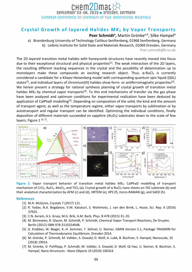
Crystal Growth of layered Halides MX3 by Vapor Transports Peer Schmidta, Martin Grönkea,b, Silke Hampelb
a) Brandenburg University of Technology Cottbus-Senftenberg, 01968 Senftenberg, Germany b) Leibniz Institute for Solid State and Materials Research, 01069 Dresden, Germany
The 2D layered transition metal halides with honeycomb structures have recently moved into focus due to their exceptional structural and physical properties[1]. The weak interaction of the 2D layers, the resulting different stacking sequences in the crystal and the possibility of delamination up to monolayers make these compounds an exciting research object. Thus, α-RuCl3 is currently considered a candidate for a Kitaev-Heisenberg model with corresponding quantum spin liquid (QSL) states[2], and individual layers of chromium(III) halides show ferro- or antiferromagnetic properties[3]. We herein present a strategy for rational synthesis planning of crystal growth of transition metal halides MX3 by chemical vapor transports[4]. To this end mechanisms of transfer via the gas phase have been analyzed and optimum conditions for experimental realization have been deduced by application of CalPhaD modelling[5]. Depending on composition of the solid, the kind and the amount of transport agent, as well as the temperature regime, either vapor transports by sublimation or by autotransport and regular transport can be identified. Optimizing the individual conditions, finally deposition of different materials succeeded on sapphire (Al2O3) substrates down to the scale of few layers, Figure 1 [6, 7].
Figure 1: Vapor transport behavior of transition metal halides MX3: CalPhaD modelling of transport mechanism of CrCl3, RuCl3, MoCl3, and TiCl3 (a); Crystal growth of α-RuCl3 nano sheets on YSZ substrate (b) and their analytical characterization by AFM (c) and (d), HRTEM (e), XPS (f), micro-RAMAN (g), and SAED (h).
References [1] M.A. McGuire, Crystals 7 (2017) 121. [2] R. Yadav, N.A. Bogdanov, V.M. Katukuri, S. Nishimoto, J. van den Brink, L. Hozoi, Sci. Rep. 6 (2016)
37925. [3] C.N. Avram, A.S. Gruia, M.G. Brik, A.M. Barb, Phys. B 478 (2015) 31−35. [4] M. Binnewies, R. Glaum, M. Schmidt, P. Schmidt, Chemical Vapor Transport Reactions, De Gruyter,
Berlin (2012) ISBN 978-3110254648. [5] G. Krabbes, W. Bieger, K.-H. Sommer, T. Söhnel, U. Steiner, GMIN Version 5.1, Package TRAGMIN for
Calculation of Thermodynamic Equilibrium, Dresden 2014. [6] M. Grönke, P. Schmidt, M. Valldor, S. Oswald, D. Wolf, A. Lubk, B. Büchner, S. Hampel, Nanoscale, 10
(2018) 19014. [7] M. Grönke, D. Pohflepp, P. Schmidt, M. Valldor, S. Oswald, D. Wolf, Qi Hao, U. Steiner, B. Büchner, S.
Hampel, Nano-Structures - Nano-Objects 19 (2019) 100324.
98
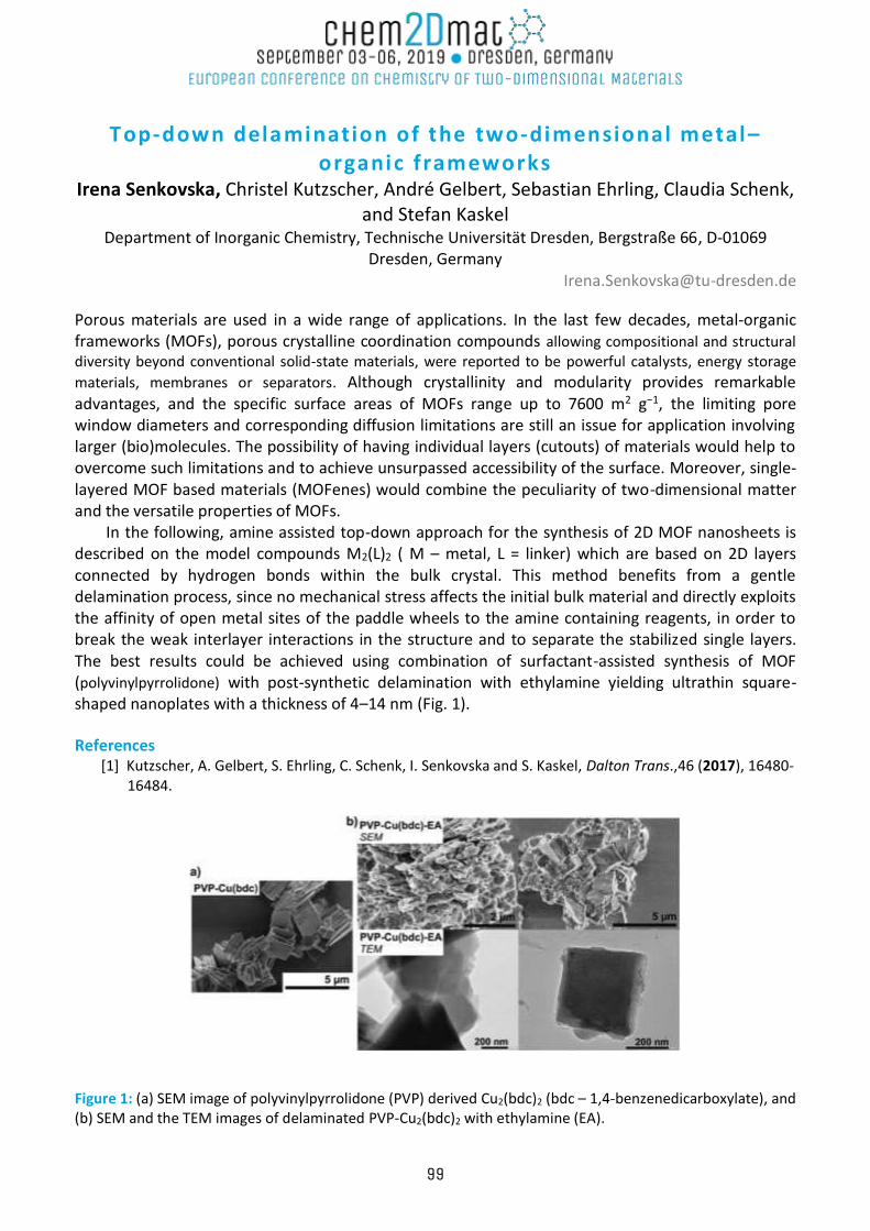
Top-down delamination of the two-dimensional metal–organic frameworks
Irena Senkovska, Christel Kutzscher, André Gelbert, Sebastian Ehrling, Claudia Schenk, and Stefan Kaskel
Department of Inorganic Chemistry, Technische Universität Dresden, Bergstraße 66, D-01069 Dresden, Germany
Porous materials are used in a wide range of applications. In the last few decades, metal-organic frameworks (MOFs), porous crystalline coordination compounds allowing compositional and structural diversity beyond conventional solid-state materials, were reported to be powerful catalysts, energy storage
materials, membranes or separators. Although crystallinity and modularity provides remarkable advantages, and the specific surface areas of MOFs range up to 7600 m2 g−1, the limiting pore window diameters and corresponding diffusion limitations are still an issue for application involving larger (bio)molecules. The possibility of having individual layers (cutouts) of materials would help to overcome such limitations and to achieve unsurpassed accessibility of the surface. Moreover, single-layered MOF based materials (MOFenes) would combine the peculiarity of two-dimensional matter and the versatile properties of MOFs.
In the following, amine assisted top-down approach for the synthesis of 2D MOF nanosheets is described on the model compounds M2(L)2 ( M – metal, L = linker) which are based on 2D layers connected by hydrogen bonds within the bulk crystal. This method benefits from a gentle delamination process, since no mechanical stress affects the initial bulk material and directly exploits the affinity of open metal sites of the paddle wheels to the amine containing reagents, in order to break the weak interlayer interactions in the structure and to separate the stabilized single layers. The best results could be achieved using combination of surfactant-assisted synthesis of MOF (polyvinylpyrrolidone) with post-synthetic delamination with ethylamine yielding ultrathin square-shaped nanoplates with a thickness of 4–14 nm (Fig. 1). References
[1] Kutzscher, A. Gelbert, S. Ehrling, C. Schenk, I. Senkovska and S. Kaskel, Dalton Trans.,46 (2017), 16480-16484.
Figure 1: (a) SEM image of polyvinylpyrrolidone (PVP) derived Cu2(bdc)2 (bdc – 1,4-benzenedicarboxylate), and (b) SEM and the TEM images of delaminated PVP-Cu2(bdc)2 with ethylamine (EA).
99
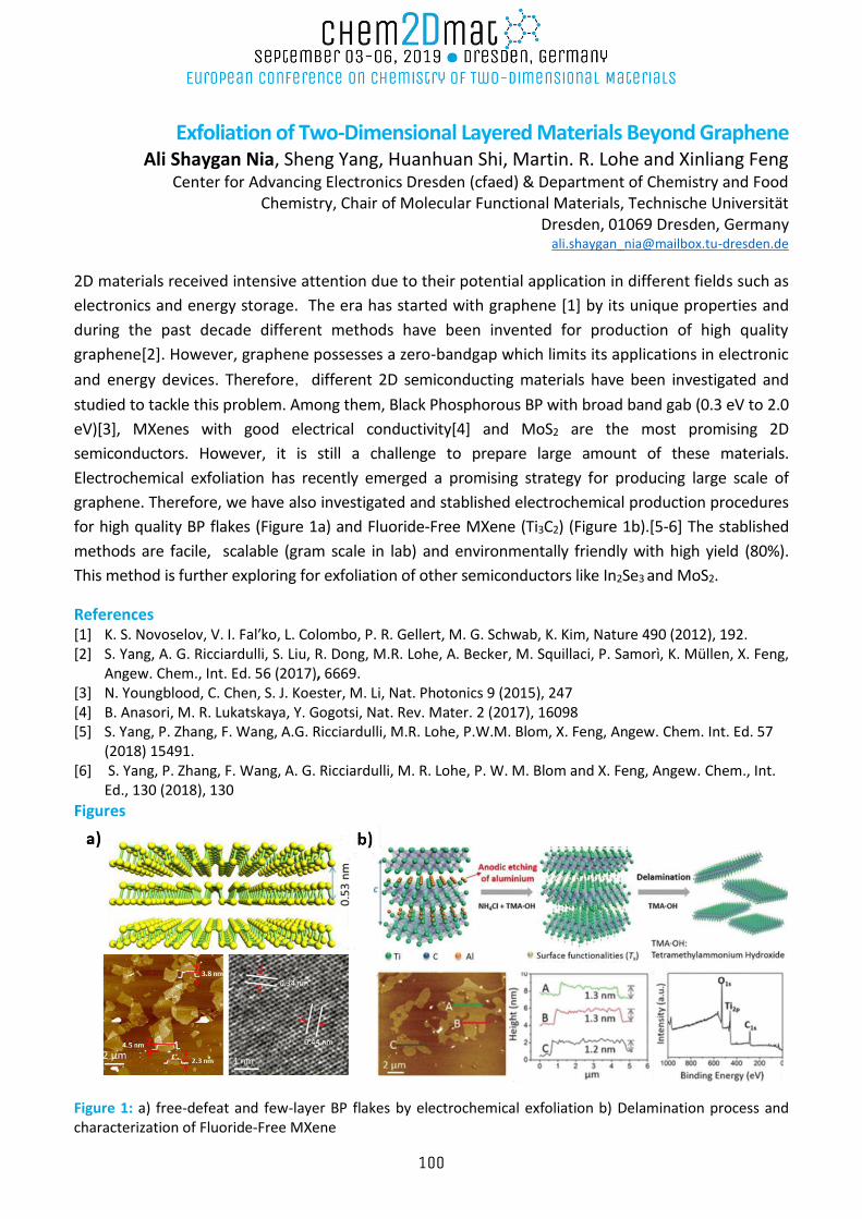
Exfoliation of Two-Dimensional Layered Materials Beyond Graphene Ali Shaygan Nia, Sheng Yang, Huanhuan Shi, Martin. R. Lohe and Xinliang Feng
Center for Advancing Electronics Dresden (cfaed) & Department of Chemistry and Food Chemistry, Chair of Molecular Functional Materials, Technische Universität
Dresden, 01069 Dresden, Germany [email protected]
2D materials received intensive attention due to their potential application in different fields such as
electronics and energy storage. The era has started with graphene [1] by its unique properties and
during the past decade different methods have been invented for production of high quality
graphene[2]. However, graphene possesses a zero-bandgap which limits its applications in electronic
and energy devices. Therefore,different 2D semiconducting materials have been investigated and
studied to tackle this problem. Among them, Black Phosphorous BP with broad band gab (0.3 eV to 2.0
eV)[3], MXenes with good electrical conductivity[4] and MoS2 are the most promising 2D
semiconductors. However, it is still a challenge to prepare large amount of these materials.
Electrochemical exfoliation has recently emerged a promising strategy for producing large scale of
graphene. Therefore, we have also investigated and stablished electrochemical production procedures
for high quality BP flakes (Figure 1a) and Fluoride-Free MXene (Ti3C2) (Figure 1b).[5-6] The stablished
methods are facile, scalable (gram scale in lab) and environmentally friendly with high yield (80%).
This method is further exploring for exfoliation of other semiconductors like In2Se3 and MoS2.
References [1] K. S. Novoselov, V. I. Fal′ko, L. Colombo, P. R. Gellert, M. G. Schwab, K. Kim, Nature 490 (2012), 192. [2] S. Yang, A. G. Ricciardulli, S. Liu, R. Dong, M.R. Lohe, A. Becker, M. Squillaci, P. Samorì, K. Müllen, X. Feng,
Angew. Chem., Int. Ed. 56 (2017), 6669. [3] N. Youngblood, C. Chen, S. J. Koester, M. Li, Nat. Photonics 9 (2015), 247 [4] B. Anasori, M. R. Lukatskaya, Y. Gogotsi, Nat. Rev. Mater. 2 (2017), 16098 [5] S. Yang, P. Zhang, F. Wang, A.G. Ricciardulli, M.R. Lohe, P.W.M. Blom, X. Feng, Angew. Chem. Int. Ed. 57
(2018) 15491. [6] S. Yang, P. Zhang, F. Wang, A. G. Ricciardulli, M. R. Lohe, P. W. M. Blom and X. Feng, Angew. Chem., Int.
Ed., 130 (2018), 130
Figures
Figure 1: a) free-defeat and few-layer BP flakes by electrochemical exfoliation b) Delamination process and characterization of Fluoride-Free MXene
100
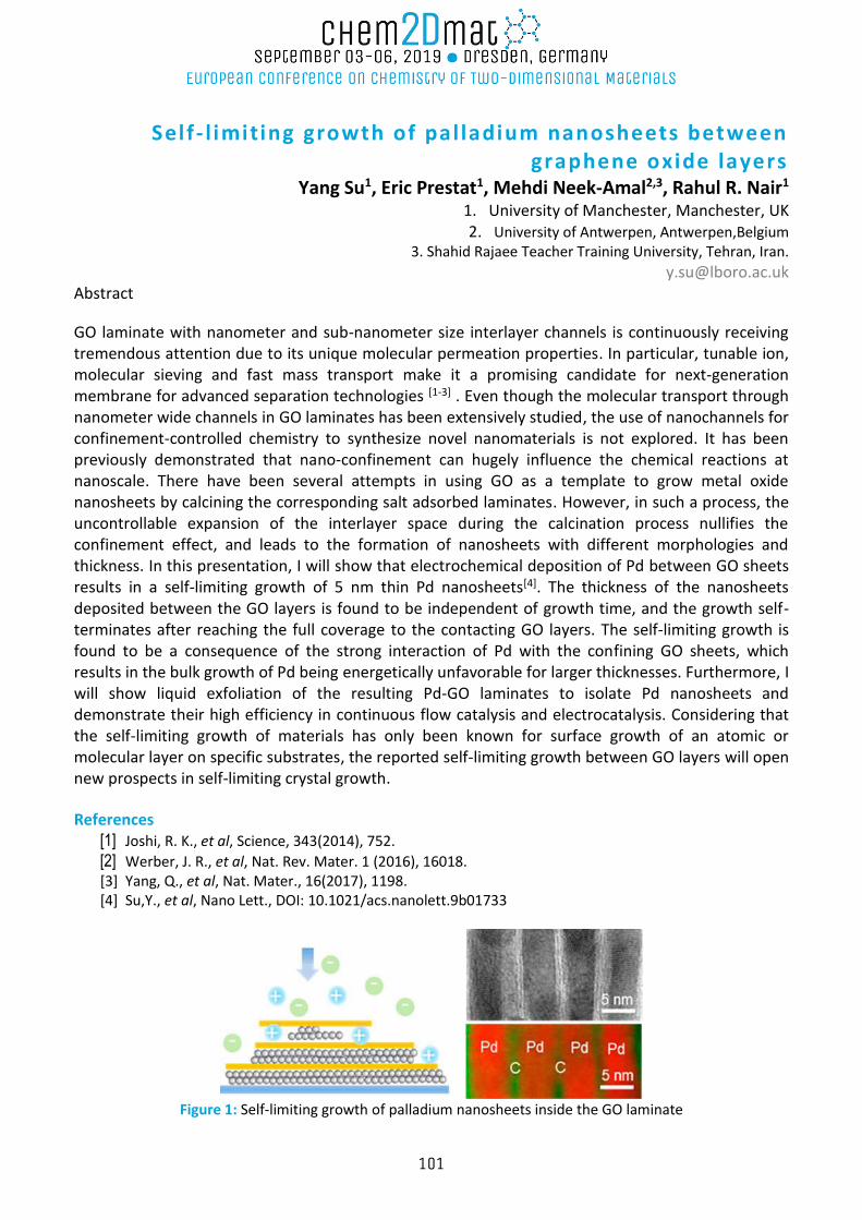
Self- l imiting growth of pal ladium nanosheets between graphene oxide layers
Yang Su1, Eric Prestat1, Mehdi Neek-Amal2,3, Rahul R. Nair1 1. University of Manchester, Manchester, UK 2. University of Antwerpen, Antwerpen,Belgium
3. Shahid Rajaee Teacher Training University, Tehran, Iran. [email protected]
Abstract
GO laminate with nanometer and sub-nanometer size interlayer channels is continuously receiving tremendous attention due to its unique molecular permeation properties. In particular, tunable ion, molecular sieving and fast mass transport make it a promising candidate for next-generation membrane for advanced separation technologies [1-3] . Even though the molecular transport through nanometer wide channels in GO laminates has been extensively studied, the use of nanochannels for confinement-controlled chemistry to synthesize novel nanomaterials is not explored. It has been previously demonstrated that nano-confinement can hugely influence the chemical reactions at nanoscale. There have been several attempts in using GO as a template to grow metal oxide nanosheets by calcining the corresponding salt adsorbed laminates. However, in such a process, the uncontrollable expansion of the interlayer space during the calcination process nullifies the confinement effect, and leads to the formation of nanosheets with different morphologies and thickness. In this presentation, I will show that electrochemical deposition of Pd between GO sheets results in a self-limiting growth of 5 nm thin Pd nanosheets[4]. The thickness of the nanosheets deposited between the GO layers is found to be independent of growth time, and the growth self-terminates after reaching the full coverage to the contacting GO layers. The self-limiting growth is found to be a consequence of the strong interaction of Pd with the confining GO sheets, which results in the bulk growth of Pd being energetically unfavorable for larger thicknesses. Furthermore, I will show liquid exfoliation of the resulting Pd-GO laminates to isolate Pd nanosheets and demonstrate their high efficiency in continuous flow catalysis and electrocatalysis. Considering that the self-limiting growth of materials has only been known for surface growth of an atomic or molecular layer on specific substrates, the reported self-limiting growth between GO layers will open new prospects in self-limiting crystal growth. References
[1] Joshi, R. K., et al, Science, 343(2014), 752.
[2] Werber, J. R., et al, Nat. Rev. Mater. 1 (2016), 16018. [3] Yang, Q., et al, Nat. Mater., 16(2017), 1198. [4] Su,Y., et al, Nano Lett., DOI: 10.1021/acs.nanolett.9b01733
Figure 1: Self-limiting growth of palladium nanosheets inside the GO laminate
101
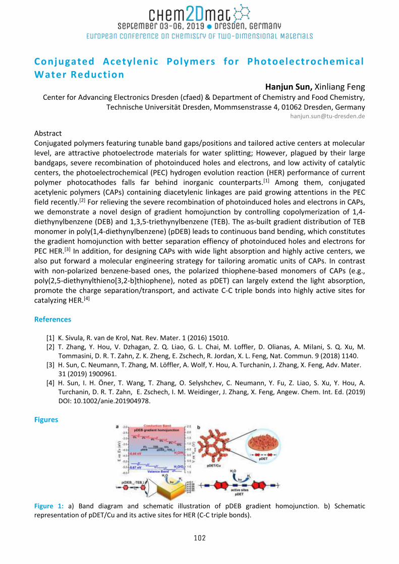
Conjugated Acetylenic Polymers for Photoelectrochemical Water Reduction
Hanjun Sun, Xinliang Feng Center for Advancing Electronics Dresden (cfaed) & Department of Chemistry and Food Chemistry,
Technische Universität Dresden, Mommsenstrasse 4, 01062 Dresden, Germany [email protected]
Abstract Conjugated polymers featuring tunable band gaps/positions and tailored active centers at molecular level, are attractive photoelectrode materials for water splitting; However, plagued by their large bandgaps, severe recombination of photoinduced holes and electrons, and low activity of catalytic centers, the photoelectrochemical (PEC) hydrogen evolution reaction (HER) performance of current polymer photocathodes falls far behind inorganic counterparts.[1] Among them, conjugated acetylenic polymers (CAPs) containing diacetylenic linkages are paid growing attentions in the PEC field recently.[2] For relieving the severe recombination of photoinduced holes and electrons in CAPs, we demonstrate a novel design of gradient homojunction by controlling copolymerization of 1,4-diethynylbenzene (DEB) and 1,3,5-triethynylbenzene (TEB). The as-built gradient distribution of TEB monomer in poly(1,4-diethynylbenzene) (pDEB) leads to continuous band bending, which constitutes the gradient homojunction with better separation effiency of photoinduced holes and electrons for PEC HER.[3] In addition, for designing CAPs with wide light absorption and highly active centers, we also put forward a molecular engineering strategy for tailoring aromatic units of CAPs. In contrast with non-polarized benzene-based ones, the polarized thiophene-based monomers of CAPs (e.g., poly(2,5-diethynylthieno[3,2-b]thiophene), noted as pDET) can largely extend the light absorption, promote the charge separation/transport, and activate C-C triple bonds into highly active sites for catalyzing HER.[4]
References [1] K. Sivula, R. van de Krol, Nat. Rev. Mater. 1 (2016) 15010. [2] T. Zhang, Y. Hou, V. Dzhagan, Z. Q. Liao, G. L. Chai, M. Loffler, D. Olianas, A. Milani, S. Q. Xu, M.
Tommasini, D. R. T. Zahn, Z. K. Zheng, E. Zschech, R. Jordan, X. L. Feng, Nat. Commun. 9 (2018) 1140. [3] H. Sun, C. Neumann, T. Zhang, M. Löffler, A. Wolf, Y. Hou, A. Turchanin, J. Zhang, X. Feng, Adv. Mater.
31 (2019) 1900961. [4] H. Sun, I. H. Öner, T. Wang, T. Zhang, O. Selyshchev, C. Neumann, Y. Fu, Z. Liao, S. Xu, Y. Hou, A.
Turchanin, D. R. T. Zahn, E. Zschech, I. M. Weidinger, J. Zhang, X. Feng, Angew. Chem. Int. Ed. (2019) DOI: 10.1002/anie.201904978.
Figures
Figure 1: a) Band diagram and schematic illustration of pDEB gradient homojunction. b) Schematic representation of pDET/Cu and its active sites for HER (C-C triple bonds).
102
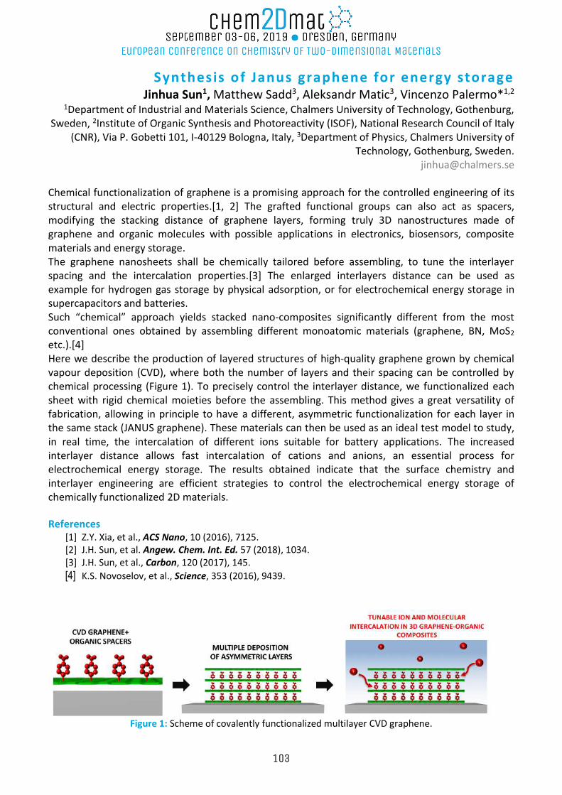
Synthesis of Janus graphene for energy storage Jinhua Sun1, Matthew Sadd3, Aleksandr Matic3, Vincenzo Palermo*1,2
1Department of Industrial and Materials Science, Chalmers University of Technology, Gothenburg, Sweden, 2Institute of Organic Synthesis and Photoreactivity (ISOF), National Research Council of Italy
(CNR), Via P. Gobetti 101, I-40129 Bologna, Italy, 3Department of Physics, Chalmers University of Technology, Gothenburg, Sweden.
[email protected] Chemical functionalization of graphene is a promising approach for the controlled engineering of its structural and electric properties.[1, 2] The grafted functional groups can also act as spacers, modifying the stacking distance of graphene layers, forming truly 3D nanostructures made of graphene and organic molecules with possible applications in electronics, biosensors, composite materials and energy storage. The graphene nanosheets shall be chemically tailored before assembling, to tune the interlayer spacing and the intercalation properties.[3] The enlarged interlayers distance can be used as example for hydrogen gas storage by physical adsorption, or for electrochemical energy storage in supercapacitors and batteries. Such “chemical” approach yields stacked nano-composites significantly different from the most conventional ones obtained by assembling different monoatomic materials (graphene, BN, MoS2 etc.).[4] Here we describe the production of layered structures of high-quality graphene grown by chemical vapour deposition (CVD), where both the number of layers and their spacing can be controlled by chemical processing (Figure 1). To precisely control the interlayer distance, we functionalized each sheet with rigid chemical moieties before the assembling. This method gives a great versatility of fabrication, allowing in principle to have a different, asymmetric functionalization for each layer in the same stack (JANUS graphene). These materials can then be used as an ideal test model to study, in real time, the intercalation of different ions suitable for battery applications. The increased interlayer distance allows fast intercalation of cations and anions, an essential process for electrochemical energy storage. The results obtained indicate that the surface chemistry and interlayer engineering are efficient strategies to control the electrochemical energy storage of chemically functionalized 2D materials. References
[1] Z.Y. Xia, et al., ACS Nano, 10 (2016), 7125. [2] J.H. Sun, et al. Angew. Chem. Int. Ed. 57 (2018), 1034. [3] J.H. Sun, et al., Carbon, 120 (2017), 145. [4] K.S. Novoselov, et al., Science, 353 (2016), 9439.
Figure 1: Scheme of covalently functionalized multilayer CVD graphene.
103
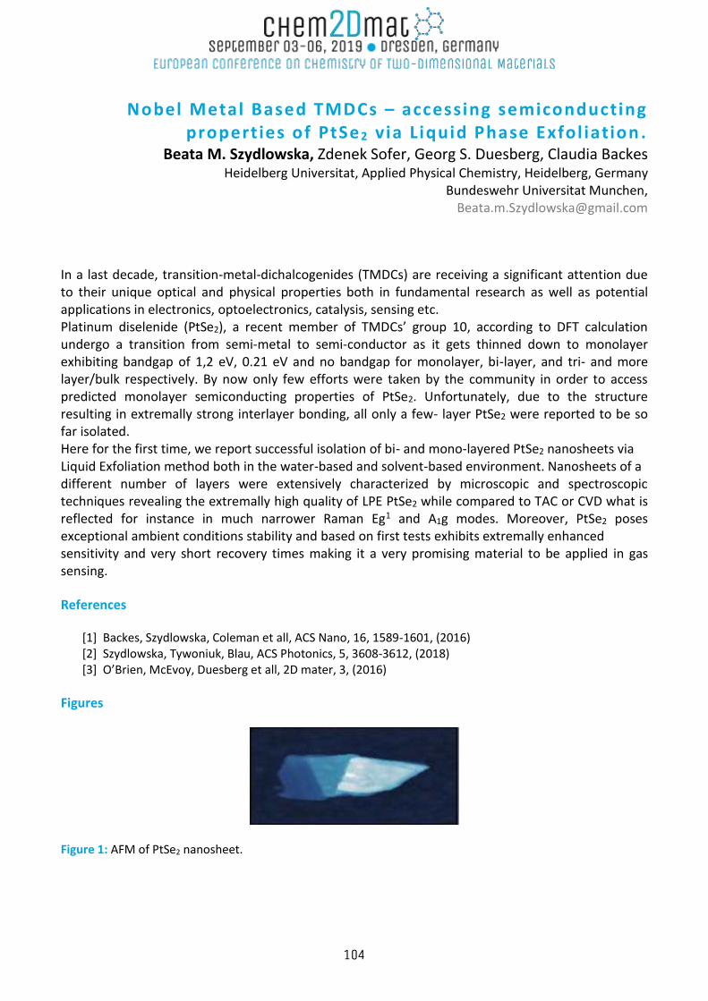
Nobel Metal Based TMDCs – accessing semiconducting propert ies of PtSe 2 v ia Liquid Phase Exfol iation .
Beata M. Szydlowska, Zdenek Sofer, Georg S. Duesberg, Claudia Backes Heidelberg Universitat, Applied Physical Chemistry, Heidelberg, Germany
Bundeswehr Universitat Munchen, [email protected]
In a last decade, transition-metal-dichalcogenides (TMDCs) are receiving a significant attention due to their unique optical and physical properties both in fundamental research as well as potential applications in electronics, optoelectronics, catalysis, sensing etc. Platinum diselenide (PtSe2), a recent member of TMDCs’ group 10, according to DFT calculation undergo a transition from semi-metal to semi-conductor as it gets thinned down to monolayer exhibiting bandgap of 1,2 eV, 0.21 eV and no bandgap for monolayer, bi-layer, and tri- and more layer/bulk respectively. By now only few efforts were taken by the community in order to access predicted monolayer semiconducting properties of PtSe2. Unfortunately, due to the structure resulting in extremally strong interlayer bonding, all only a few- layer PtSe2 were reported to be so far isolated. Here for the first time, we report successful isolation of bi- and mono-layered PtSe2 nanosheets via Liquid Exfoliation method both in the water-based and solvent-based environment. Nanosheets of a different number of layers were extensively characterized by microscopic and spectroscopic techniques revealing the extremally high quality of LPE PtSe2 while compared to TAC or CVD what is reflected for instance in much narrower Raman Eg1 and A1g modes. Moreover, PtSe2 poses exceptional ambient conditions stability and based on first tests exhibits extremally enhanced sensitivity and very short recovery times making it a very promising material to be applied in gas sensing.
References
[1] Backes, Szydlowska, Coleman et all, ACS Nano, 16, 1589-1601, (2016) [2] Szydlowska, Tywoniuk, Blau, ACS Photonics, 5, 3608-3612, (2018) [3] O’Brien, McEvoy, Duesberg et all, 2D mater, 3, (2016)
Figures
Figure 1: AFM of PtSe2 nanosheet.
104
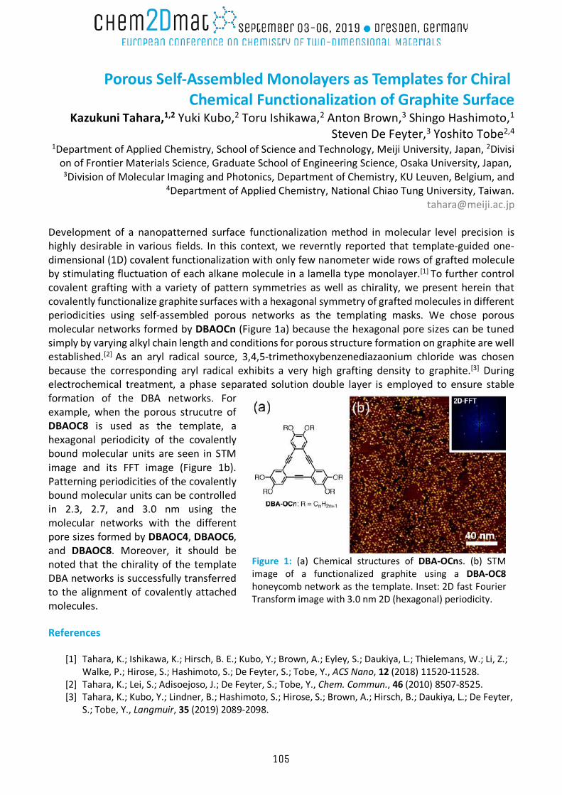
Porous Self-Assembled Monolayers as Templates for Chiral Chemical Functionalization of Graphite Surface
Kazukuni Tahara,1,2 Yuki Kubo,2 Toru Ishikawa,2 Anton Brown,3 Shingo Hashimoto,1 Steven De Feyter,3 Yoshito Tobe2,4
1Department of Applied Chemistry, School of Science and Technology, Meiji University, Japan, 2Division of Frontier Materials Science, Graduate School of Engineering Science, Osaka University, Japan,
3Division of Molecular Imaging and Photonics, Department of Chemistry, KU Leuven, Belgium, and 4Department of Applied Chemistry, National Chiao Tung University, Taiwan.
[email protected] Development of a nanopatterned surface functionalization method in molecular level precision is highly desirable in various fields. In this context, we reverntly reported that template-guided one-dimensional (1D) covalent functionalization with only few nanometer wide rows of grafted molecule by stimulating fluctuation of each alkane molecule in a lamella type monolayer.[1] To further control covalent grafting with a variety of pattern symmetries as well as chirality, we present herein that covalently functionalize graphite surfaces with a hexagonal symmetry of grafted molecules in different periodicities using self-assembled porous networks as the templating masks. We chose porous molecular networks formed by DBAOCn (Figure 1a) because the hexagonal pore sizes can be tuned simply by varying alkyl chain length and conditions for porous structure formation on graphite are well established.[2] As an aryl radical source, 3,4,5-trimethoxybenzenediazaonium chloride was chosen because the corresponding aryl radical exhibits a very high grafting density to graphite.[3] During electrochemical treatment, a phase separated solution double layer is employed to ensure stable formation of the DBA networks. For example, when the porous strucutre of DBAOC8 is used as the template, a hexagonal periodicity of the covalently bound molecular units are seen in STM image and its FFT image (Figure 1b). Patterning periodicities of the covalently bound molecular units can be controlled in 2.3, 2.7, and 3.0 nm using the molecular networks with the different pore sizes formed by DBAOC4, DBAOC6, and DBAOC8. Moreover, it should be noted that the chirality of the template DBA networks is successfully transferred to the alignment of covalently attached molecules. References
[1] Tahara, K.; Ishikawa, K.; Hirsch, B. E.; Kubo, Y.; Brown, A.; Eyley, S.; Daukiya, L.; Thielemans, W.; Li, Z.; Walke, P.; Hirose, S.; Hashimoto, S.; De Feyter, S.; Tobe, Y., ACS Nano, 12 (2018) 11520-11528.
[2] Tahara, K.; Lei, S.; Adisoejoso, J.; De Feyter, S.; Tobe, Y., Chem. Commun., 46 (2010) 8507-8525. [3] Tahara, K.; Kubo, Y.; Lindner, B.; Hashimoto, S.; Hirose, S.; Brown, A.; Hirsch, B.; Daukiya, L.; De Feyter,
S.; Tobe, Y., Langmuir, 35 (2019) 2089-2098.
Figure 1: (a) Chemical structures of DBA-OCns. (b) STM image of a functionalized graphite using a DBA-OC8 honeycomb network as the template. Inset: 2D fast Fourier Transform image with 3.0 nm 2D (hexagonal) periodicity.
105
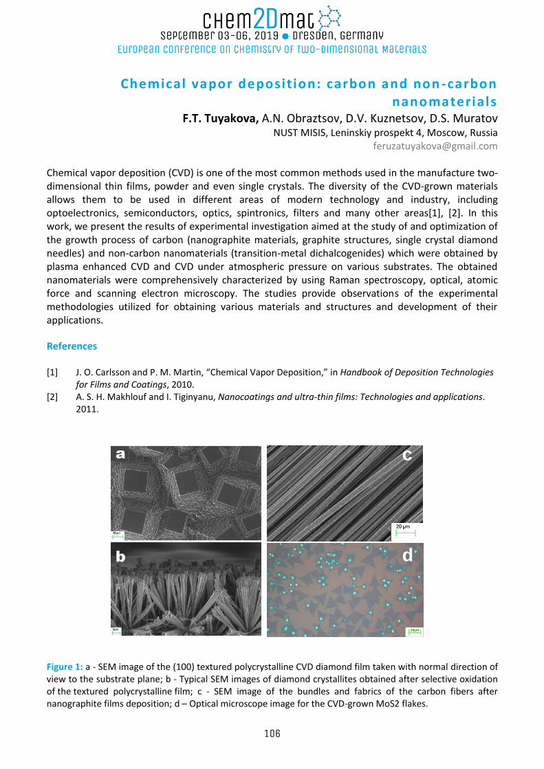
Chemical vapor deposition: carbon and non -carbon nanomaterials
F.T. Tuyakova, A.N. Obraztsov, D.V. Kuznetsov, D.S. Muratov NUST MISIS, Leninskiy prospekt 4, Moscow, Russia
Chemical vapor deposition (CVD) is one of the most common methods used in the manufacture two-dimensional thin films, powder and even single crystals. The diversity of the CVD-grown materials allows them to be used in different areas of modern technology and industry, including optoelectronics, semiconductors, optics, spintronics, filters and many other areas[1], [2]. In this work, we present the results of experimental investigation aimed at the study of and optimization of the growth process of carbon (nanographite materials, graphite structures, single crystal diamond needles) and non-carbon nanomaterials (transition-metal dichalcogenides) which were obtained by plasma enhanced CVD and CVD under atmospheric pressure on various substrates. The obtained nanomaterials were comprehensively characterized by using Raman spectroscopy, optical, atomic force and scanning electron microscopy. The studies provide observations of the experimental methodologies utilized for obtaining various materials and structures and development of their applications. References [1] J. O. Carlsson and P. M. Martin, “Chemical Vapor Deposition,” in Handbook of Deposition Technologies
for Films and Coatings, 2010. [2] A. S. H. Makhlouf and I. Tiginyanu, Nanocoatings and ultra-thin films: Technologies and applications.
2011.
Figure 1: a - SEM image of the (100) textured polycrystalline CVD diamond film taken with normal direction of view to the substrate plane; b - Typical SEM images of diamond crystallites obtained after selective oxidation of the textured polycrystalline film; c - SEM image of the bundles and fabrics of the carbon fibers after nanographite films deposition; d – Optical microscope image for the CVD-grown MoS2 flakes.
10 µm
d
c
d
10µm
106
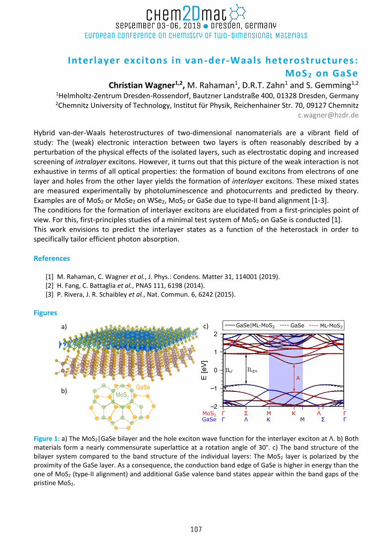
Interlayer excitons in van -der-Waals heterostructures : MoS 2 on GaSe
Christian Wagner1,2, M. Rahaman1, D.R.T. Zahn1 and S. Gemming1,2 1Helmholtz-Zentrum Dresden-Rossendorf, Bautzner Landstraße 400, 01328 Dresden, Germany 2Chemnitz University of Technology, Institut für Physik, Reichenhainer Str. 70, 09127 Chemnitz
Hybrid van-der-Waals heterostructures of two-dimensional nanomaterials are a vibrant field of study: The (weak) electronic interaction between two layers is often reasonably described by a perturbation of the physical effects of the isolated layers, such as electrostatic doping and increased screening of intralayer excitons. However, it turns out that this picture of the weak interaction is not exhaustive in terms of all optical properties: the formation of bound excitons from electrons of one layer and holes from the other layer yields the formation of interlayer excitons. These mixed states are measured experimentally by photoluminescence and photocurrents and predicted by theory. Examples are of MoS2 or MoSe2 on WSe2, MoS2 or GaSe due to type-II band alignment [1-3]. The conditions for the formation of interlayer excitons are elucidated from a first-principles point of view. For this, first-principles studies of a minimal test system of MoS2 on GaSe is conducted [1]. This work envisions to predict the interlayer states as a function of the heterostack in order to specifically tailor efficient photon absorption. References
[1] M. Rahaman, C. Wagner et al., J. Phys.: Condens. Matter 31, 114001 (2019). [2] H. Fang, C. Battaglia et al., PNAS 111, 6198 (2014). [3] P. Rivera, J. R. Schaibley et al., Nat. Commun. 6, 6242 (2015).
Figures
Figure 1: a) The MoS2|GaSe bilayer and the hole exciton wave function for the interlayer exciton at Λ. b) Both materials form a nearly commensurate superlattice at a rotation angle of 30°. c) The band structure of the bilayer system compared to the band structure of the individual layers: The MoS2 layer is polarized by the proximity of the GaSe layer. As a consequence, the conduction band edge of GaSe is higher in energy than the one of MoS2 (type-II alignment) and additional GaSe valence band states appear within the band gaps of the pristine MoS2.
MoS2 GaSe b)
a) c)
107
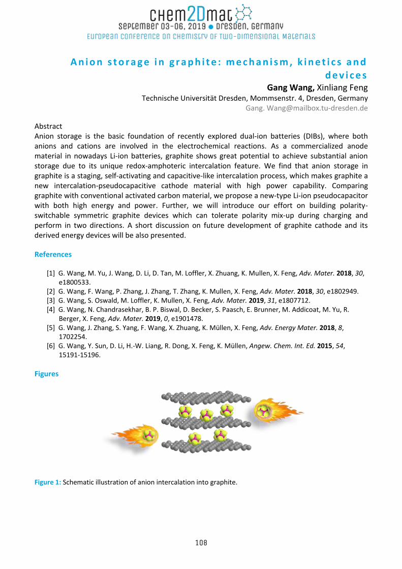
A n i o n s t o r a g e i n g r a p h i t e : m e c h a n i s m , k i n e t i c s a n d d e v i c e s
Gang Wang, Xinliang Feng Technische Universität Dresden, Mommsenstr. 4, Dresden, Germany
Gang. [email protected]
Abstract Anion storage is the basic foundation of recently explored dual-ion batteries (DIBs), where both anions and cations are involved in the electrochemical reactions. As a commercialized anode material in nowadays Li-ion batteries, graphite shows great potential to achieve substantial anion storage due to its unique redox-amphoteric intercalation feature. We find that anion storage in graphite is a staging, self-activating and capacitive-like intercalation process, which makes graphite a new intercalation-pseudocapacitive cathode material with high power capability. Comparing graphite with conventional activated carbon material, we propose a new-type Li-ion pseudocapacitor with both high energy and power. Further, we will introduce our effort on building polarity-switchable symmetric graphite devices which can tolerate polarity mix-up during charging and perform in two directions. A short discussion on future development of graphite cathode and its derived energy devices will be also presented.
References
[1] G. Wang, M. Yu, J. Wang, D. Li, D. Tan, M. Loffler, X. Zhuang, K. Mullen, X. Feng, Adv. Mater. 2018, 30, e1800533.
[2] G. Wang, F. Wang, P. Zhang, J. Zhang, T. Zhang, K. Mullen, X. Feng, Adv. Mater. 2018, 30, e1802949. [3] G. Wang, S. Oswald, M. Loffler, K. Mullen, X. Feng, Adv. Mater. 2019, 31, e1807712. [4] G. Wang, N. Chandrasekhar, B. P. Biswal, D. Becker, S. Paasch, E. Brunner, M. Addicoat, M. Yu, R.
Berger, X. Feng, Adv. Mater. 2019, 0, e1901478. [5] G. Wang, J. Zhang, S. Yang, F. Wang, X. Zhuang, K. Müllen, X. Feng, Adv. Energy Mater. 2018, 8,
1702254. [6] G. Wang, Y. Sun, D. Li, H.-W. Liang, R. Dong, X. Feng, K. Müllen, Angew. Chem. Int. Ed. 2015, 54,
15191-15196.
Figures
Figure 1: Schematic illustration of anion intercalation into graphite.
108
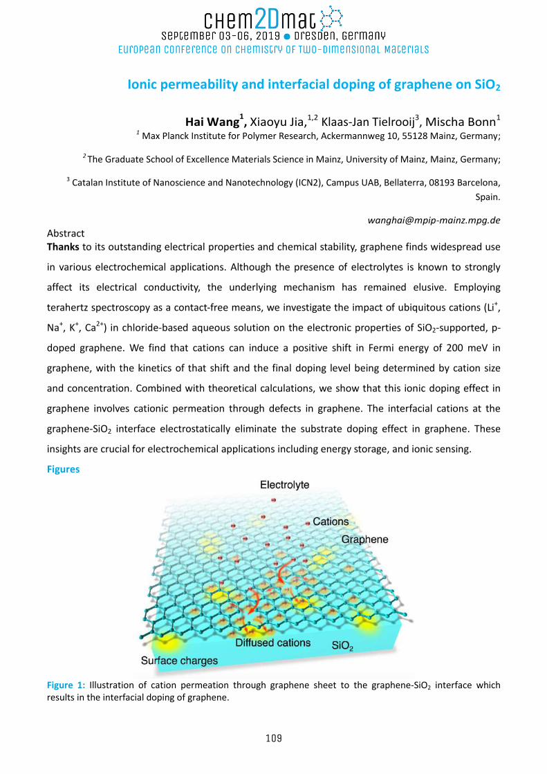
Ionic permeability and interfacial doping of graphene on SiO2
Hai Wang1, Xiaoyu Jia,1,2 Klaas-Jan Tielrooij3, Mischa Bonn1
1 Max Planck Institute for Polymer Research, Ackermannweg 10, 55128 Mainz, Germany;
2 The Graduate School of Excellence Materials Science in Mainz, University of Mainz, Mainz, Germany;
3 Catalan Institute of Nanoscience and Nanotechnology (ICN2), Campus UAB, Bellaterra, 08193 Barcelona,
Spain.
Abstract Thanks to its outstanding electrical properties and chemical stability, graphene finds widespread use
in various electrochemical applications. Although the presence of electrolytes is known to strongly
affect its electrical conductivity, the underlying mechanism has remained elusive. Employing
terahertz spectroscopy as a contact-free means, we investigate the impact of ubiquitous cations (Li+,
Na+, K+, Ca2+) in chloride-based aqueous solution on the electronic properties of SiO2-supported, p-
doped graphene. We find that cations can induce a positive shift in Fermi energy of 200 meV in
graphene, with the kinetics of that shift and the final doping level being determined by cation size
and concentration. Combined with theoretical calculations, we show that this ionic doping effect in
graphene involves cationic permeation through defects in graphene. The interfacial cations at the
graphene-SiO2 interface electrostatically eliminate the substrate doping effect in graphene. These
insights are crucial for electrochemical applications including energy storage, and ionic sensing.
Figures
Figure 1: Illustration of cation permeation through graphene sheet to the graphene-SiO2 interface which results in the interfacial doping of graphene.
109
Engineering of Nanographenes with Doping and Pores Kun Xu
TU Dresden, Dresden, Germany [email protected]
Nanographenes are important organic materials due to their great potential in electronics, optoelectronics and spintronics. The top-down synthesis of nanographenes via exfoliation presents well-known disadvantages such as non-regular edge structures or uncontrollable sizes. In contrast, the bottom-up organic synthesis approach has emerged in the last decades as a powerful tool to design structurally well-defined nanographenes. Here two different bottom-up approaches have been developed to engineer the structure and energy gap of nanographenes. In the first example, cationic nitrogen and helicity were introduced into nanographenes via solution synthesis. The obtained molecules exhibit unique nonplanar configurations with axial chirality, lower lying HOMOs/LUMOs and energy gaps, as well as quasi reversible electrochemical reduction. In the second case, through a combined solution and on-surface synthesis approach, non-planar nanopores were introduced into nanographene. The porous nanographene exhibits an increased energy gap and nonplanar configuration.
References
[1] J. Wu et al, Chem. Rev., 107 (2007) 718-747. [2] K. Xu et al, Angew. Chem. Int. Ed., 56 (2017) 15876-15881. [3] K. Xu et al, J. Am. Chem. Soc., 141 (2019) 7726-7730.
110
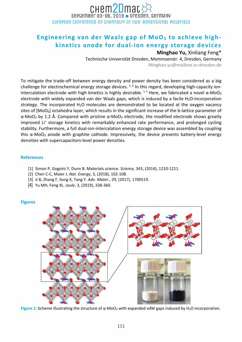
Engineering van der Waals gap of MoO 3 to achieve high-kinetics anode for dual- ion energy storage devices
Minghao Yu, Xinliang Feng* Technische Universität Dresden, Mommsenstr. 4, Dresden, Germany
To mitigate the trade-off between energy density and power density has been considered as a big challenge for electrochemical energy storage devices. 1, 2 In this regard, developing high-capacity ion-intercalation electrode with high kinetics is highly desirable. 3, 4 Here, we fabricated a novel α-MoO3 electrode with widely expanded van der Waals gaps, which is induced by a facile H2O-incorporation strategy. The incorporated H2O molecules are demonstrated to be located at the oxygen vacancy sites of [MoO6] octahedra layer, which results in the significant increase of the b-lattice parameter of α-MoO3 by 1.2 Å. Compared with pristine α-MoO3 electrode, the modified electrode shows greatly improved Li+ storage kinetics with remarkably enhanced rate performance, and prolonged cycling stability. Furthermore, a full dual-ion-intercalation energy storage device was assembled by coupling this α-MoO3 anode with graphite cathode. Impressively, the device presents battery-level energy densities with supercapacitors-level power densities. References
[1] Simon P, Gogotsi Y, Dunn B. Materials science. Science, 343, (2014), 1210-1211. [2] Chen C-C, Maier J. Nat. Energy, 3, (2018), 102-108. [3] Ji B, Zhang F, Song X, Tang Y. Adv. Mater., 29, (2017), 1700519.
[4] Yu MH, Feng XL. Joule, 3, (2019), 338-360. Figures
Figure 1: Scheme illustrating the structure of α-MoO3 with expanded vdW gaps induced by H2O incorporation.
111
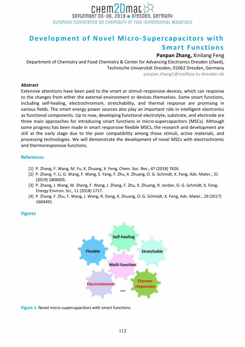
De ve lop ment o f N o vel Mic ro -Supe rc ap ac i to rs w i th Smart Fun ct ion s
Panpan Zhang, Xinliang Feng Department of Chemistry and Food Chemistry & Center for Advancing Electronics Dresden (cfaed),
Technische Universität Dresden, 01062 Dresden, Germany [email protected]
Abstract Extensive attentions have been paid to the smart or stimuli-responsive devices, which can response to the changes from either the external environment or devices themselves. Some smart functions, including self-healing, electrochromism, stretchability, and thermal response are promising in various fields. The smart energy power sources also play an important role in intelligent electronics as functional components. Up to now, developing functional electrolyte, substrate, and electrode are three main approaches for introducing smart functions in micro-supercapacitors (MSCs). Although some progress has been made in smart responsive flexible MSCs, the research and development are still at the early stage due to the poor compatibility among those stimuli, active materials, and processing technologies. We will demonstrate the development of novel MSCs with electrochromic and thermoresponsive functions.
References
[1] P. Zhang, F. Wang, M. Yu, X. Zhuang, X. Feng, Chem. Soc. Rev., 47 (2018) 7426. [2] P. Zhang, Y. Li, G. Wang, F. Wang, S. Yang, F. Zhu, X. Zhuang, O. G. Schmidt, X. Feng, Adv. Mater., 31
(2019) 1806005. [3] P. Zhang, J. Wang, W. Sheng, F. Wang, J. Zhang, F. Zhu, X. Zhuang, R. Jordan, O. G. Schmidt, X. Feng,
Energy Environ. Sci., 11 (2018) 1717. [4] P. Zhang, F. Zhu, F. Wang, J. Wang, R. Dong, X. Zhuang, O. G. Schmidt, X. Feng, Adv. Mater., 29 (2017)
1604491.
Figures
Figure 1: Novel micro-supercapacitors with smart functions.
112
Rational Synthesis of Two-Dimensional Conducting Polymer Crystals
Tao Zhang1, Haoyuan Qi2, Zhongquan Liao3, Ehrenfried Zschech3, Ute Kaiser2, Xinliang Feng1
1Faculty of Chemistry and Food Chemistry, Technische Universität Dresden, 01062 Dresden,
Germany. 2Central Facility of Electron Microscopy, Electron Microscopy Group of Materials Science, Universität
Ulm, 89081 Ulm, Germany. 3Fraunhofer Institute for Ceramic Technologies and Systems (IKTS), Maria-Reiche-Strasse 2, 01109
Dresden, Germany.
Abstract The discovery of linear conducting polymers made of organic monomers has led to unprecedented excitement over their potential applications in organic electronics. It is well known that structural disorder hinders efficient charge transport in conducting polymer films, thus degrading device performance [1]. To achieve long-range charge transport, one intriguing strategy is to align the linear conducting polymer chains into two-dimensional (2D) thin films [2]. The 2D thin film, with high-degree of molecular ordering (i.e. fully expanded-coil conformation) via supramolecular assembly by interchain interactions, can provide multiple pathways for interchain charge transport and bypass possible defects of individual polymer chains. Therefore, there is a long standing dream to achieve the synthesis of 2D conducting polymers to maximize interchain delocalization and achieve 2D delocalized transport [3]. In this talk, I will present a novel air-water interfacial methodology for the synthesis of 2D conducting polymers with controllable crystallinity, lateral size, orientation and crosslinking [4].
References [1] Noriega, R., Rivnay, J., Vandewal, K., et al. Nat. Mater., 12 (2013), 1038. [2] Kang, S. D., Snyder, G. J. Nat. Mater., 16 (2017), 252. [3] Sirringhaus, H., Brown, P. J., Friend, R. H., et al. Nature, 401 (1999), 685. [4] Zhang, T., Qi, H. Y., Liao, Z. Q., Zschech, E., Kaiser, U., Feng, X. L., et al. Submitted.
113

POSTERS
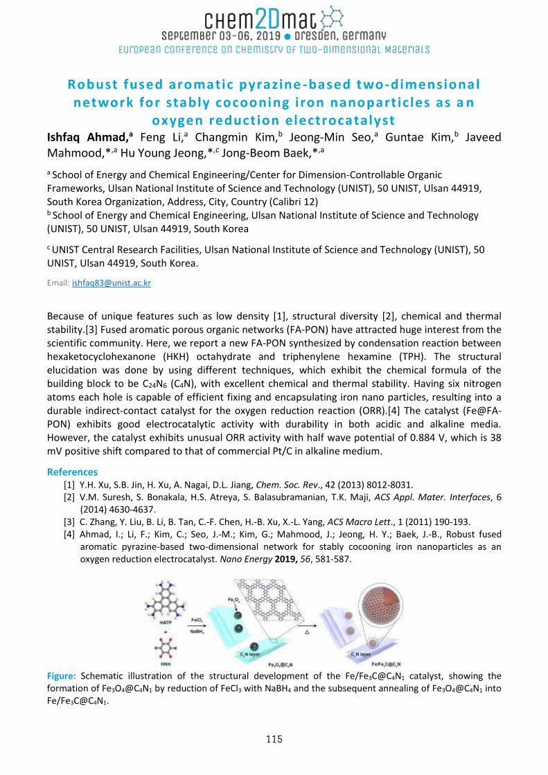
Robust fused aromatic pyrazine -based two-dimensional network for stably cocooning i ron nanopart ic les as a n
oxygen reduction electrocatalyst Ishfaq Ahmad,a Feng Li,a Changmin Kim,b Jeong-Min Seo,a Guntae Kim,b Javeed Mahmood,*,a Hu Young Jeong,*,c Jong-Beom Baek,*,a
a School of Energy and Chemical Engineering/Center for Dimension-Controllable Organic Frameworks, Ulsan National Institute of Science and Technology (UNIST), 50 UNIST, Ulsan 44919, South Korea Organization, Address, City, Country (Calibri 12) b School of Energy and Chemical Engineering, Ulsan National Institute of Science and Technology (UNIST), 50 UNIST, Ulsan 44919, South Korea
c UNIST Central Research Facilities, Ulsan National Institute of Science and Technology (UNIST), 50 UNIST, Ulsan 44919, South Korea.
Email: [email protected]
Because of unique features such as low density [1], structural diversity [2], chemical and thermal stability.[3] Fused aromatic porous organic networks (FA-PON) have attracted huge interest from the scientific community. Here, we report a new FA-PON synthesized by condensation reaction between hexaketocyclohexanone (HKH) octahydrate and triphenylene hexamine (TPH). The structural elucidation was done by using different techniques, which exhibit the chemical formula of the building block to be C24N6 (C4N), with excellent chemical and thermal stability. Having six nitrogen atoms each hole is capable of efficient fixing and encapsulating iron nano particles, resulting into a durable indirect-contact catalyst for the oxygen reduction reaction (ORR).[4] The catalyst (Fe@FA-PON) exhibits good electrocatalytic activity with durability in both acidic and alkaline media. However, the catalyst exhibits unusual ORR activity with half wave potential of 0.884 V, which is 38 mV positive shift compared to that of commercial Pt/C in alkaline medium.
References [1] Y.H. Xu, S.B. Jin, H. Xu, A. Nagai, D.L. Jiang, Chem. Soc. Rev., 42 (2013) 8012-8031. [2] V.M. Suresh, S. Bonakala, H.S. Atreya, S. Balasubramanian, T.K. Maji, ACS Appl. Mater. Interfaces, 6
(2014) 4630-4637. [3] C. Zhang, Y. Liu, B. Li, B. Tan, C.-F. Chen, H.-B. Xu, X.-L. Yang, ACS Macro Lett., 1 (2011) 190-193. [4] Ahmad, I.; Li, F.; Kim, C.; Seo, J.-M.; Kim, G.; Mahmood, J.; Jeong, H. Y.; Baek, J.-B., Robust fused
aromatic pyrazine-based two-dimensional network for stably cocooning iron nanoparticles as an oxygen reduction electrocatalyst. Nano Energy 2019, 56, 581-587.
Figure: Schematic illustration of the structural development of the Fe/Fe3C@C4N1 catalyst, showing the formation of Fe3O4@C4N1 by reduction of FeCl3 with NaBH4 and the subsequent annealing of Fe3O4@C4N1 into Fe/Fe3C@C4N1.
115
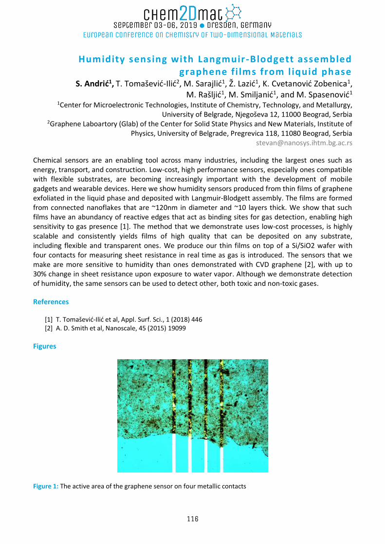
Humidity sensing with Langmuir-Blodgett assembled graphene fi lms from l iquid phase
S. Andrić1, T. Tomašević-Ilić2, M. Sarajlić1, Ž. Lazić1, K. Cvetanović Zobenica1, M. Rašljić1, M. Smiljanić1, and M. Spasenović1
1Center for Microelectronic Technologies, Institute of Chemistry, Technology, and Metallurgy, University of Belgrade, Njegoševa 12, 11000 Beograd, Serbia
2Graphene Laboartory (Glab) of the Center for Solid State Physics and New Materials, Institute of Physics, University of Belgrade, Pregrevica 118, 11080 Beograd, Serbia
Chemical sensors are an enabling tool across many industries, including the largest ones such as energy, transport, and construction. Low-cost, high performance sensors, especially ones compatible with flexible substrates, are becoming increasingly important with the development of mobile gadgets and wearable devices. Here we show humidity sensors produced from thin films of graphene exfoliated in the liquid phase and deposited with Langmuir-Blodgett assembly. The films are formed from connected nanoflakes that are ~120nm in diameter and ~10 layers thick. We show that such films have an abundancy of reactive edges that act as binding sites for gas detection, enabling high sensitivity to gas presence [1]. The method that we demonstrate uses low-cost processes, is highly scalable and consistently yields films of high quality that can be deposited on any substrate, including flexible and transparent ones. We produce our thin films on top of a Si/SiO2 wafer with four contacts for measuring sheet resistance in real time as gas is introduced. The sensors that we make are more sensitive to humidity than ones demonstrated with CVD graphene [2], with up to 30% change in sheet resistance upon exposure to water vapor. Although we demonstrate detection of humidity, the same sensors can be used to detect other, both toxic and non-toxic gases.
References
[1] T. Tomašević-Ilić et al, Appl. Surf. Sci., 1 (2018) 446 [2] A. D. Smith et al, Nanoscale, 45 (2015) 19099
Figures
Figure 1: The active area of the graphene sensor on four metallic contacts
116
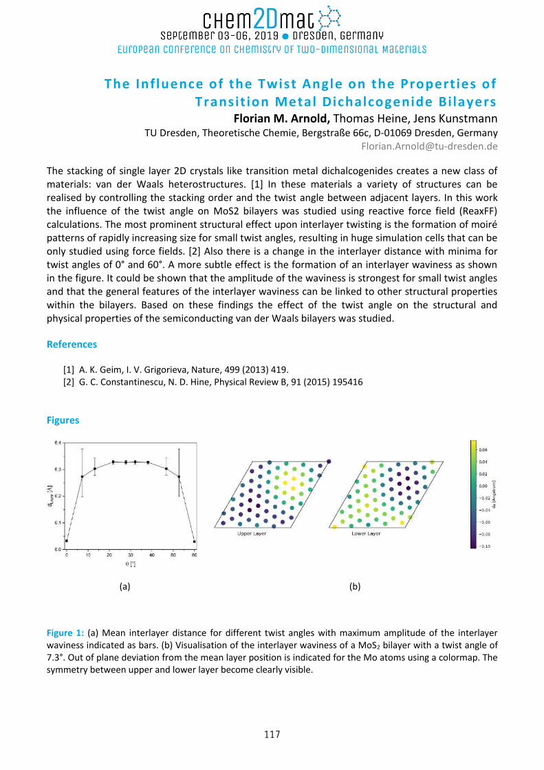
The Influence of the Twist Angle on the Propert ies of Transit ion Metal Dichalcogenide Bi layers
Florian M. Arnold, Thomas Heine, Jens Kunstmann TU Dresden, Theoretische Chemie, Bergstraße 66c, D-01069 Dresden, Germany
The stacking of single layer 2D crystals like transition metal dichalcogenides creates a new class of materials: van der Waals heterostructures. [1] In these materials a variety of structures can be realised by controlling the stacking order and the twist angle between adjacent layers. In this work the influence of the twist angle on MoS2 bilayers was studied using reactive force field (ReaxFF) calculations. The most prominent structural effect upon interlayer twisting is the formation of moiré patterns of rapidly increasing size for small twist angles, resulting in huge simulation cells that can be only studied using force fields. [2] Also there is a change in the interlayer distance with minima for twist angles of 0° and 60°. A more subtle effect is the formation of an interlayer waviness as shown in the figure. It could be shown that the amplitude of the waviness is strongest for small twist angles and that the general features of the interlayer waviness can be linked to other structural properties within the bilayers. Based on these findings the effect of the twist angle on the structural and physical properties of the semiconducting van der Waals bilayers was studied. References
[1] A. K. Geim, I. V. Grigorieva, Nature, 499 (2013) 419. [2] G. C. Constantinescu, N. D. Hine, Physical Review B, 91 (2015) 195416
Figures
(a) (b)
Figure 1: (a) Mean interlayer distance for different twist angles with maximum amplitude of the interlayer waviness indicated as bars. (b) Visualisation of the interlayer waviness of a MoS2 bilayer with a twist angle of 7.3°. Out of plane deviation from the mean layer position is indicated for the Mo atoms using a colormap. The symmetry between upper and lower layer become clearly visible.
117
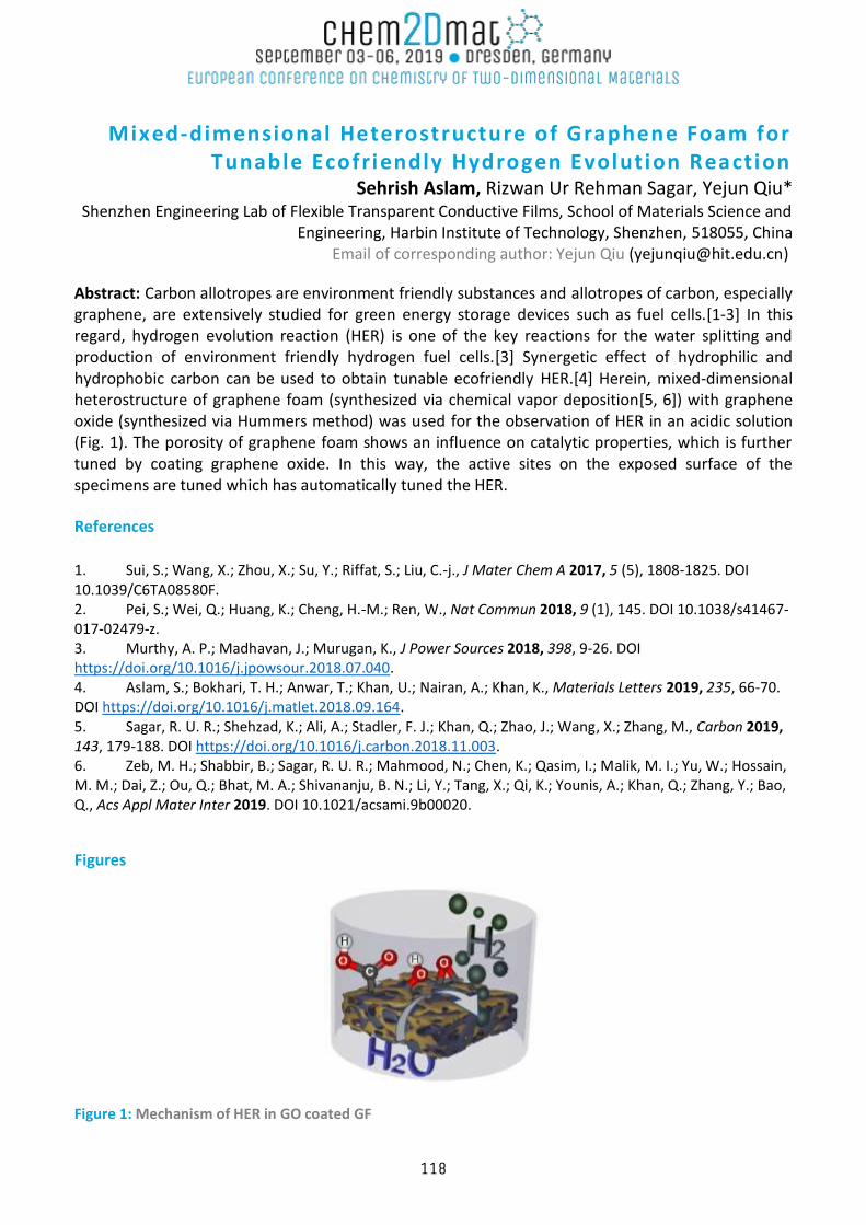
Mixed-dimensional Heterostructure of Graphene Foam for Tunable Ecofriendly Hydrogen Evolution Reaction
Sehrish Aslam, Rizwan Ur Rehman Sagar, Yejun Qiu* Shenzhen Engineering Lab of Flexible Transparent Conductive Films, School of Materials Science and
Engineering, Harbin Institute of Technology, Shenzhen, 518055, China Email of corresponding author: Yejun Qiu ([email protected])
Abstract: Carbon allotropes are environment friendly substances and allotropes of carbon, especially graphene, are extensively studied for green energy storage devices such as fuel cells.[1-3] In this regard, hydrogen evolution reaction (HER) is one of the key reactions for the water splitting and production of environment friendly hydrogen fuel cells.[3] Synergetic effect of hydrophilic and hydrophobic carbon can be used to obtain tunable ecofriendly HER.[4] Herein, mixed-dimensional heterostructure of graphene foam (synthesized via chemical vapor deposition[5, 6]) with graphene oxide (synthesized via Hummers method) was used for the observation of HER in an acidic solution (Fig. 1). The porosity of graphene foam shows an influence on catalytic properties, which is further tuned by coating graphene oxide. In this way, the active sites on the exposed surface of the specimens are tuned which has automatically tuned the HER. References
1. Sui, S.; Wang, X.; Zhou, X.; Su, Y.; Riffat, S.; Liu, C.-j., J Mater Chem A 2017, 5 (5), 1808-1825. DOI 10.1039/C6TA08580F. 2. Pei, S.; Wei, Q.; Huang, K.; Cheng, H.-M.; Ren, W., Nat Commun 2018, 9 (1), 145. DOI 10.1038/s41467-017-02479-z. 3. Murthy, A. P.; Madhavan, J.; Murugan, K., J Power Sources 2018, 398, 9-26. DOI https://doi.org/10.1016/j.jpowsour.2018.07.040. 4. Aslam, S.; Bokhari, T. H.; Anwar, T.; Khan, U.; Nairan, A.; Khan, K., Materials Letters 2019, 235, 66-70. DOI https://doi.org/10.1016/j.matlet.2018.09.164. 5. Sagar, R. U. R.; Shehzad, K.; Ali, A.; Stadler, F. J.; Khan, Q.; Zhao, J.; Wang, X.; Zhang, M., Carbon 2019, 143, 179-188. DOI https://doi.org/10.1016/j.carbon.2018.11.003. 6. Zeb, M. H.; Shabbir, B.; Sagar, R. U. R.; Mahmood, N.; Chen, K.; Qasim, I.; Malik, M. I.; Yu, W.; Hossain, M. M.; Dai, Z.; Ou, Q.; Bhat, M. A.; Shivananju, B. N.; Li, Y.; Tang, X.; Qi, K.; Younis, A.; Khan, Q.; Zhang, Y.; Bao, Q., Acs Appl Mater Inter 2019. DOI 10.1021/acsami.9b00020.
Figures
Figure 1: Mechanism of HER in GO coated GF
118
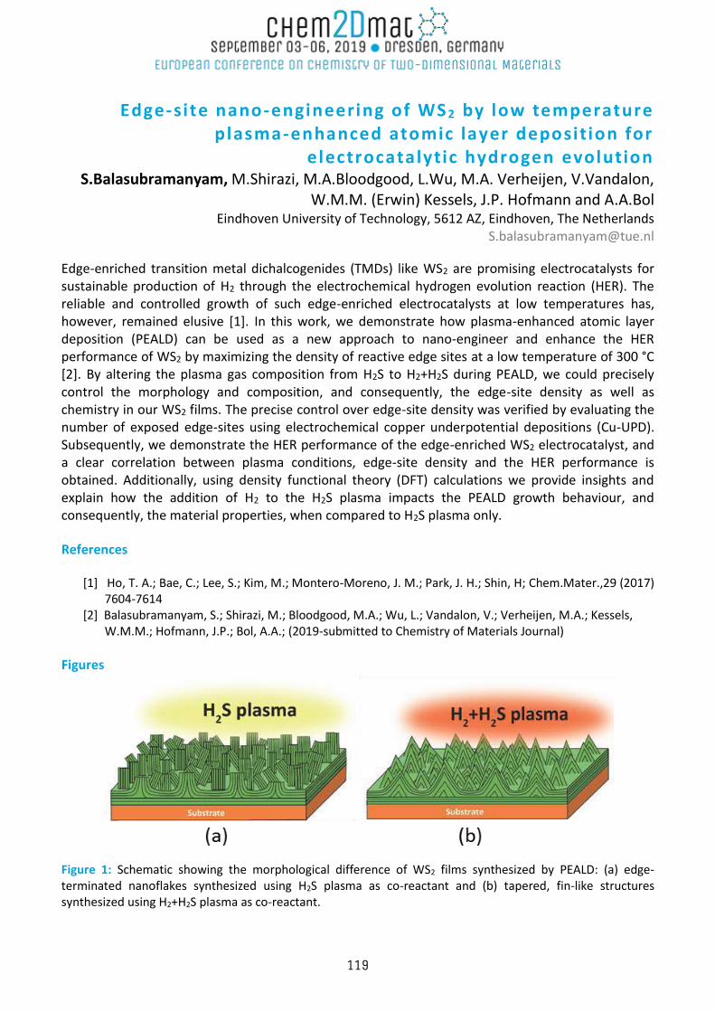
Edge-site nano-engineering of WS 2 by low temperature plasma-enhanced atomic layer deposition for
e lectrocatalytic hydrogen evolution S.Balasubramanyam, M.Shirazi, M.A.Bloodgood, L.Wu, M.A. Verheijen, V.Vandalon,
W.M.M. (Erwin) Kessels, J.P. Hofmann and A.A.Bol Eindhoven University of Technology, 5612 AZ, Eindhoven, The Netherlands
Edge-enriched transition metal dichalcogenides (TMDs) like WS2 are promising electrocatalysts for sustainable production of H2 through the electrochemical hydrogen evolution reaction (HER). The reliable and controlled growth of such edge-enriched electrocatalysts at low temperatures has, however, remained elusive [1]. In this work, we demonstrate how plasma-enhanced atomic layer deposition (PEALD) can be used as a new approach to nano-engineer and enhance the HER performance of WS2 by maximizing the density of reactive edge sites at a low temperature of 300 °C [2]. By altering the plasma gas composition from H2S to H2+H2S during PEALD, we could precisely control the morphology and composition, and consequently, the edge-site density as well as chemistry in our WS2 films. The precise control over edge-site density was verified by evaluating the number of exposed edge-sites using electrochemical copper underpotential depositions (Cu-UPD). Subsequently, we demonstrate the HER performance of the edge-enriched WS2 electrocatalyst, and a clear correlation between plasma conditions, edge-site density and the HER performance is obtained. Additionally, using density functional theory (DFT) calculations we provide insights and explain how the addition of H2 to the H2S plasma impacts the PEALD growth behaviour, and consequently, the material properties, when compared to H2S plasma only.
References
[1] Ho, T. A.; Bae, C.; Lee, S.; Kim, M.; Montero-Moreno, J. M.; Park, J. H.; Shin, H; Chem.Mater.,29 (2017) 7604-7614
[2] Balasubramanyam, S.; Shirazi, M.; Bloodgood, M.A.; Wu, L.; Vandalon, V.; Verheijen, M.A.; Kessels, W.M.M.; Hofmann, J.P.; Bol, A.A.; (2019-submitted to Chemistry of Materials Journal)
Figures
Figure 1: Schematic showing the morphological difference of WS2 films synthesized by PEALD: (a) edge-terminated nanoflakes synthesized using H2S plasma as co-reactant and (b) tapered, fin-like structures synthesized using H2+H2S plasma as co-reactant.
119
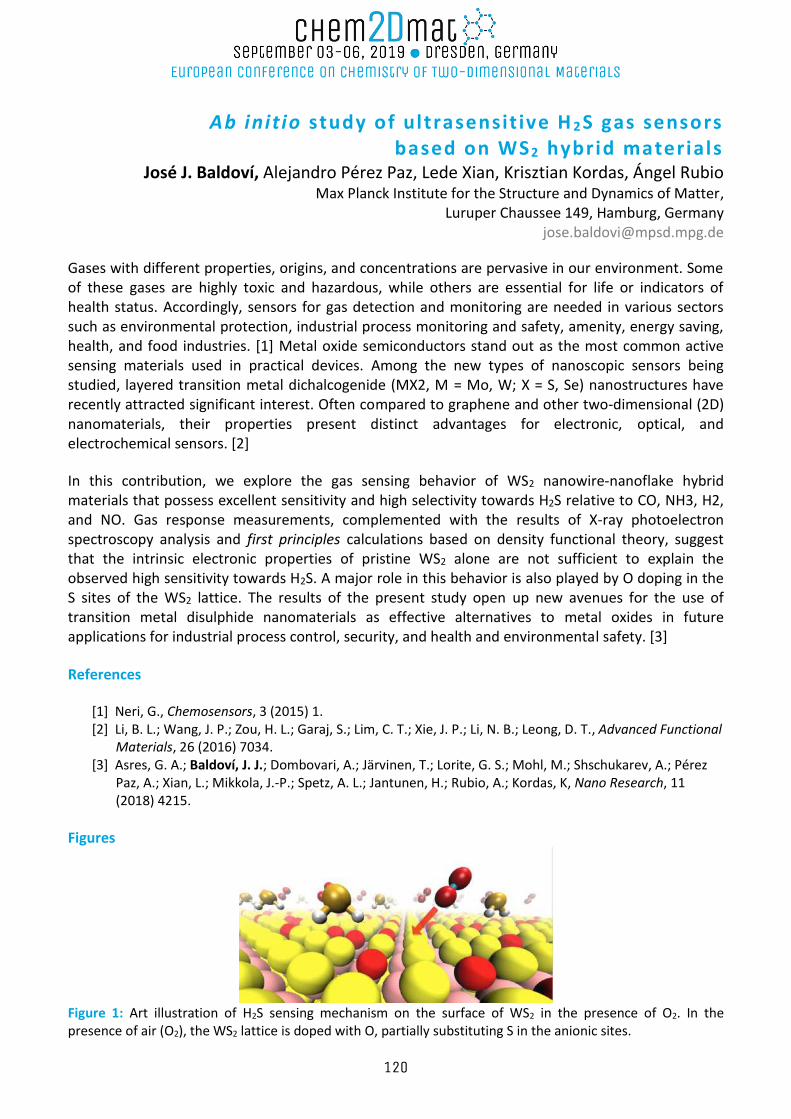
Ab initio study of ultrasensit ive H 2 S gas sensors based on WS2 hybrid materials
José J. Baldoví, Alejandro Pérez Paz, Lede Xian, Krisztian Kordas, Ángel Rubio Max Planck Institute for the Structure and Dynamics of Matter,
Luruper Chaussee 149, Hamburg, Germany [email protected]
Gases with different properties, origins, and concentrations are pervasive in our environment. Some of these gases are highly toxic and hazardous, while others are essential for life or indicators of health status. Accordingly, sensors for gas detection and monitoring are needed in various sectors such as environmental protection, industrial process monitoring and safety, amenity, energy saving, health, and food industries. [1] Metal oxide semiconductors stand out as the most common active sensing materials used in practical devices. Among the new types of nanoscopic sensors being studied, layered transition metal dichalcogenide (MX2, M = Mo, W; X = S, Se) nanostructures have recently attracted significant interest. Often compared to graphene and other two-dimensional (2D) nanomaterials, their properties present distinct advantages for electronic, optical, and electrochemical sensors. [2]
In this contribution, we explore the gas sensing behavior of WS2 nanowire-nanoflake hybrid materials that possess excellent sensitivity and high selectivity towards H2S relative to CO, NH3, H2, and NO. Gas response measurements, complemented with the results of X-ray photoelectron spectroscopy analysis and first principles calculations based on density functional theory, suggest that the intrinsic electronic properties of pristine WS2 alone are not sufficient to explain the observed high sensitivity towards H2S. A major role in this behavior is also played by O doping in the S sites of the WS2 lattice. The results of the present study open up new avenues for the use of transition metal disulphide nanomaterials as effective alternatives to metal oxides in future applications for industrial process control, security, and health and environmental safety. [3] References
[1] Neri, G., Chemosensors, 3 (2015) 1. [2] Li, B. L.; Wang, J. P.; Zou, H. L.; Garaj, S.; Lim, C. T.; Xie, J. P.; Li, N. B.; Leong, D. T., Advanced Functional
Materials, 26 (2016) 7034. [3] Asres, G. A.; Baldoví, J. J.; Dombovari, A.; Järvinen, T.; Lorite, G. S.; Mohl, M.; Shschukarev, A.; Pérez
Paz, A.; Xian, L.; Mikkola, J.-P.; Spetz, A. L.; Jantunen, H.; Rubio, A.; Kordas, K, Nano Research, 11 (2018) 4215.
Figures
Figure 1: Art illustration of H2S sensing mechanism on the surface of WS2 in the presence of O2. In the presence of air (O2), the WS2 lattice is doped with O, partially substituting S in the anionic sites.
120
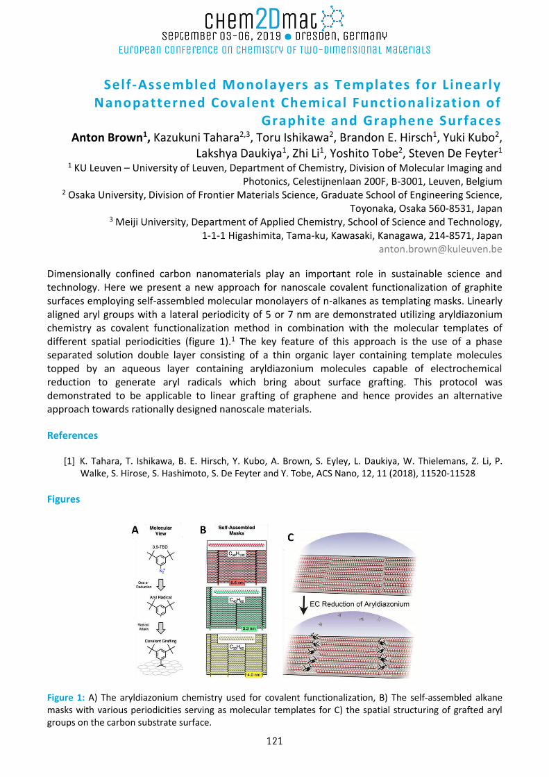
Self-Assembled Monolayers as Templates for Linearly Nanopatterned Covalent Chemical Functionalizat ion of
Graphite and Graphene Surfaces Anton Brown1, Kazukuni Tahara2,3, Toru Ishikawa2, Brandon E. Hirsch1, Yuki Kubo2,
Lakshya Daukiya1, Zhi Li1, Yoshito Tobe2, Steven De Feyter1 1 KU Leuven – University of Leuven, Department of Chemistry, Division of Molecular Imaging and
Photonics, Celestijnenlaan 200F, B-3001, Leuven, Belgium 2 Osaka University, Division of Frontier Materials Science, Graduate School of Engineering Science,
Toyonaka, Osaka 560-8531, Japan 3 Meiji University, Department of Applied Chemistry, School of Science and Technology,
1-1-1 Higashimita, Tama-ku, Kawasaki, Kanagawa, 214-8571, Japan [email protected]
Dimensionally confined carbon nanomaterials play an important role in sustainable science and technology. Here we present a new approach for nanoscale covalent functionalization of graphite surfaces employing self-assembled molecular monolayers of n-alkanes as templating masks. Linearly aligned aryl groups with a lateral periodicity of 5 or 7 nm are demonstrated utilizing aryldiazonium chemistry as covalent functionalization method in combination with the molecular templates of different spatial periodicities (figure 1).1 The key feature of this approach is the use of a phase separated solution double layer consisting of a thin organic layer containing template molecules topped by an aqueous layer containing aryldiazonium molecules capable of electrochemical reduction to generate aryl radicals which bring about surface grafting. This protocol was demonstrated to be applicable to linear grafting of graphene and hence provides an alternative approach towards rationally designed nanoscale materials.
References
[1] K. Tahara, T. Ishikawa, B. E. Hirsch, Y. Kubo, A. Brown, S. Eyley, L. Daukiya, W. Thielemans, Z. Li, P. Walke, S. Hirose, S. Hashimoto, S. De Feyter and Y. Tobe, ACS Nano, 12, 11 (2018), 11520-11528
Figures
Figure 1: A) The aryldiazonium chemistry used for covalent functionalization, B) The self-assembled alkane masks with various periodicities serving as molecular templates for C) the spatial structuring of grafted aryl groups on the carbon substrate surface.
121
Electrochemical Exfol iation of Black Phosphorus Alexandra Burger, Gonzalo Abellán, Frank Hauke, and Andreas Hirsch
Chair of Organic Chemistry II & Joint Institute of Advanced Materials and Processes (ZMP) Friedrich-Alexander-Universität Erlangen-Nürnberg (FAU), Nikolaus-Fiebiger-Straße 10
91058 Erlangen, Germany [email protected]
Black phosphorus (BP) has recently attracted great attention due to its tunable, layer-dependent bandgap, high carrier mobility, good current on/off ratio, as well as unique in-plane anisotropy, which renders the material attractive for nanoelectronic, thermoelectric and photonic devices.[1] The major challenge for a successful application lies in the fabrication of few- or single layer nanosheets of BP. Several methods have been developed, while mechanical and liquid exfoliation of the bulk crystals figure amongst the most prominent ones.[2] However, large-scale exfoliation leading to uniform and stable dispersions in high yield remains a challenge. At this point, electrochemical driven exfoliation, which has been successfully employed for graphene and other 2D materials, yielding nanosheets in good quality and high yield, emerged as an attractive alternative. Herein, we focus on the electrochemical exfoliation of BP. We present a screening of different electrolytes, reaction conditions, solvents and ionic liquids,[3] and their effects on both, the exfoliation process itself and on the quality of the obtained BP nanosheets.
References
[1] A. Hirsch, F. Hauke, Angew. Chem. Int. Ed. 2017, 57, 4338. [2] D. Hanlon, C. Backes, E. Doherty, C. S. Cucinotta, N. C. Berner, C. Boland, K. Lee, A. Harvey, P. Lynch, Z.
Gholamvand, S. Zhang, K. Wang, G. Moynihan, A. Pokle, Q. M. Ramasse, N. McEvoy, W. J. Blau, J. Wang, G. Abellan, F. Hauke, A. Hirsch, S. Sanvito, D. D. O'Regan, G. S. Duesberg, V. Nicolosi, J. N. Coleman, Nature communications 2015, 6, 8563.
[3] G. Abellán, S. Wild, V. Lloret, N. Scheuschner, R. Gillen, U. Mundloch, J. Maultzsch, M. Varela, F. Hauke, A. Hirsch, JACS 2017, 139, 10432.
122
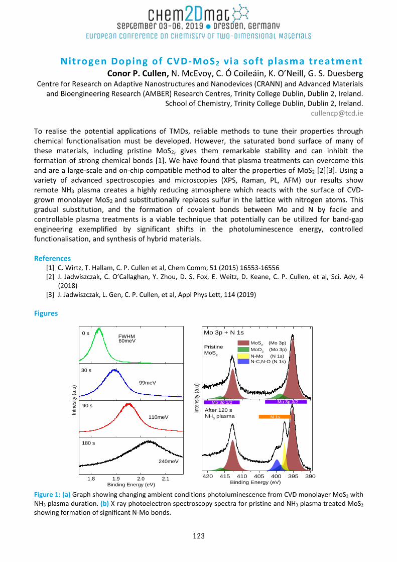
Nitrogen Doping of CVD-MoS2 v ia soft plasma treatment Conor P. Cullen, N. McEvoy, C. Ó Coileáin, K. O’Neill, G. S. Duesberg
Centre for Research on Adaptive Nanostructures and Nanodevices (CRANN) and Advanced Materials and Bioengineering Research (AMBER) Research Centres, Trinity College Dublin, Dublin 2, Ireland.
School of Chemistry, Trinity College Dublin, Dublin 2, Ireland. [email protected]
To realise the potential applications of TMDs, reliable methods to tune their properties through chemical functionalisation must be developed. However, the saturated bond surface of many of these materials, including pristine MoS2, gives them remarkable stability and can inhibit the formation of strong chemical bonds [1]. We have found that plasma treatments can overcome this and are a large-scale and on-chip compatible method to alter the properties of MoS2 [2][3]. Using a variety of advanced spectroscopies and microscopies (XPS, Raman, PL, AFM) our results show remote NH3 plasma creates a highly reducing atmosphere which reacts with the surface of CVD-grown monolayer MoS2 and substitutionally replaces sulfur in the lattice with nitrogen atoms. This gradual substitution, and the formation of covalent bonds between Mo and N by facile and controllable plasma treatments is a viable technique that potentially can be utilized for band-gap engineering exemplified by significant shifts in the photoluminescence energy, controlled functionalisation, and synthesis of hybrid materials. References
[1] C. Wirtz, T. Hallam, C. P. Cullen et al, Chem Comm, 51 (2015) 16553-16556 [2] J. Jadwiszczak, C. O’Callaghan, Y. Zhou, D. S. Fox, E. Weitz, D. Keane, C. P. Cullen, et al, Sci. Adv, 4
(2018) [3] J. Jadwiszczak, L. Gen, C. P. Cullen, et al, Appl Phys Lett, 114 (2019)
Figures
1.9 2.11.8 2.0
FWHM
180 s
90 s
30 s
60meV
110meV
99meV
240meV
0 s
Intn
esi
ty (
a.u
)
Binding Energy (eV)
420 415 410 405 400 395 390
After 120 s
NH3 plasma
Binding Energy (eV)
Inte
nsi
ty (
a.u
)
Pristine
MoS2
Mo 3p + N 1s
MoS2 (Mo 3p)
MoO3 (Mo 3p)
N-Mo (N 1s)
N-C,N-O (N 1s)
Mo 3p 3/2Mo 3p 1/2
N 1s
Figure 1: (a) Graph showing changing ambient conditions photoluminescence from CVD monolayer MoS2 with NH3 plasma duration. (b) X-ray photoelectron spectroscopy spectra for pristine and NH3 plasma treated MoS2 showing formation of significant N-Mo bonds.
123
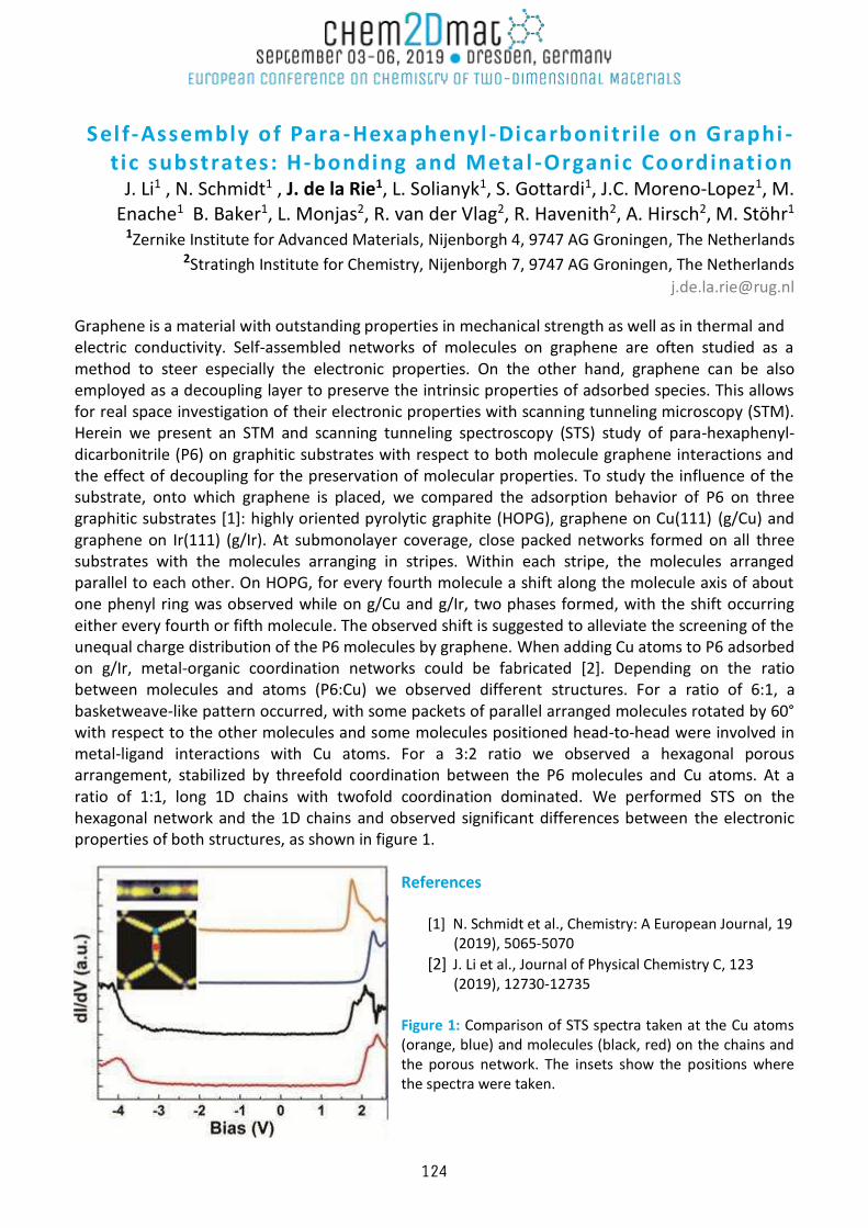
Sel f-Assembly of Para-Hexaphenyl -Dicarbonitri le on Graphi -t ic substrates: H-bonding and Metal -Organic Coordination
J. Li1 , N. Schmidt1 , J. de la Rie1, L. Solianyk1, S. Gottardi1, J.C. Moreno-Lopez1, M. Enache1 B. Baker1, L. Monjas2, R. van der Vlag2, R. Havenith2, A. Hirsch2, M. Stöhr1
1Zernike Institute for Advanced Materials, Nijenborgh 4, 9747 AG Groningen, The Netherlands 2Stratingh Institute for Chemistry, Nijenborgh 7, 9747 AG Groningen, The Netherlands
Graphene is a material with outstanding properties in mechanical strength as well as in thermal and electric conductivity. Self-assembled networks of molecules on graphene are often studied as a method to steer especially the electronic properties. On the other hand, graphene can be also employed as a decoupling layer to preserve the intrinsic properties of adsorbed species. This allows for real space investigation of their electronic properties with scanning tunneling microscopy (STM). Herein we present an STM and scanning tunneling spectroscopy (STS) study of para-hexaphenyl-dicarbonitrile (P6) on graphitic substrates with respect to both molecule graphene interactions and the effect of decoupling for the preservation of molecular properties. To study the influence of the substrate, onto which graphene is placed, we compared the adsorption behavior of P6 on three graphitic substrates [1]: highly oriented pyrolytic graphite (HOPG), graphene on Cu(111) (g/Cu) and graphene on Ir(111) (g/Ir). At submonolayer coverage, close packed networks formed on all three substrates with the molecules arranging in stripes. Within each stripe, the molecules arranged parallel to each other. On HOPG, for every fourth molecule a shift along the molecule axis of about one phenyl ring was observed while on g/Cu and g/Ir, two phases formed, with the shift occurring either every fourth or fifth molecule. The observed shift is suggested to alleviate the screening of the unequal charge distribution of the P6 molecules by graphene. When adding Cu atoms to P6 adsorbed on g/Ir, metal-organic coordination networks could be fabricated [2]. Depending on the ratio between molecules and atoms (P6:Cu) we observed different structures. For a ratio of 6:1, a basketweave-like pattern occurred, with some packets of parallel arranged molecules rotated by 60° with respect to the other molecules and some molecules positioned head-to-head were involved in metal-ligand interactions with Cu atoms. For a 3:2 ratio we observed a hexagonal porous arrangement, stabilized by threefold coordination between the P6 molecules and Cu atoms. At a ratio of 1:1, long 1D chains with twofold coordination dominated. We performed STS on the hexagonal network and the 1D chains and observed significant differences between the electronic properties of both structures, as shown in figure 1.
References
[1] N. Schmidt et al., Chemistry: A European Journal, 19 (2019), 5065-5070
[2] J. Li et al., Journal of Physical Chemistry C, 123 (2019), 12730-12735
Figure 1: Comparison of STS spectra taken at the Cu atoms (orange, blue) and molecules (black, red) on the chains and the porous network. The insets show the positions where the spectra were taken.
124
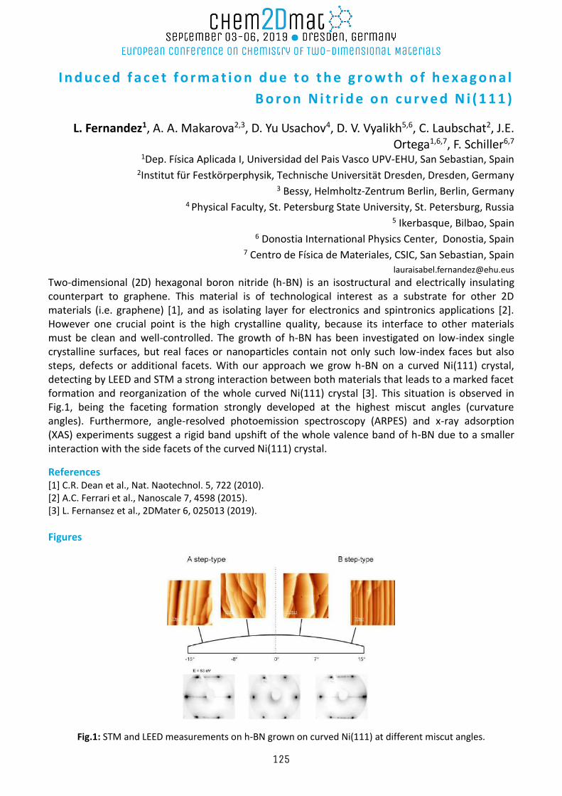
I n d u c e d f a c e t f o r m a t i o n d u e t o t h e g r o w t h o f h e x a g o n a l
B o r o n N i t r i d e o n c u r v e d N i ( 1 1 1 )
L. Fernandez1, A. A. Makarova2,3, D. Yu Usachov4, D. V. Vyalikh5,6, C. Laubschat2, J.E. Ortega1,6,7, F. Schiller6,7
1Dep. Física Aplicada I, Universidad del Pais Vasco UPV-EHU, San Sebastian, Spain 2Institut für Festkörperphysik, Technische Universität Dresden, Dresden, Germany
3 Bessy, Helmholtz-Zentrum Berlin, Berlin, Germany 4 Physical Faculty, St. Petersburg State University, St. Petersburg, Russia
5 Ikerbasque, Bilbao, Spain 6 Donostia International Physics Center, Donostia, Spain
7 Centro de Física de Materiales, CSIC, San Sebastian, Spain
Two-dimensional (2D) hexagonal boron nitride (h-BN) is an isostructural and electrically insulating counterpart to graphene. This material is of technological interest as a substrate for other 2D materials (i.e. graphene) [1], and as isolating layer for electronics and spintronics applications [2]. However one crucial point is the high crystalline quality, because its interface to other materials must be clean and well-controlled. The growth of h-BN has been investigated on low-index single crystalline surfaces, but real faces or nanoparticles contain not only such low-index faces but also steps, defects or additional facets. With our approach we grow h-BN on a curved Ni(111) crystal, detecting by LEED and STM a strong interaction between both materials that leads to a marked facet formation and reorganization of the whole curved Ni(111) crystal [3]. This situation is observed in Fig.1, being the faceting formation strongly developed at the highest miscut angles (curvature angles). Furthermore, angle-resolved photoemission spectroscopy (ARPES) and x-ray adsorption (XAS) experiments suggest a rigid band upshift of the whole valence band of h-BN due to a smaller interaction with the side facets of the curved Ni(111) crystal.
References [1] C.R. Dean et al., Nat. Naotechnol. 5, 722 (2010). [2] A.C. Ferrari et al., Nanoscale 7, 4598 (2015). [3] L. Fernansez et al., 2DMater 6, 025013 (2019).
Figures
Fig.1: STM and LEED measurements on h-BN grown on curved Ni(111) at different miscut angles.
125
Exfol iation, oxidation and functionalization of antimonene Michael Fickert,1,2 Mhamed Assebban,1,2 Carlos Gibaja,3 Frank Hauke, 1,2 Andreas
Hirsch, 1,2 Félix Zamora,3,* Gonzalo Abellan1,2,4* 1Zentralinstitut für Neue Materialien und Prozesstechnik (ZMP), Fürth, Germany
2Organic Chemistry II, FAU Erlangen/Nürnberg, Erlangen, Germany 3Departamento de Química Inorgánica, Institute for Advanced Research in Chemical Sciences
(IAdChem) Universidad Autónoma de Madrid, Spain 4Institute of Molecular Science,University of Valencia, Valencia, Spain
In recent years two dimensional (2D) materials like graphene, transition metal dichalcogenides, and more recently black phosphorus are receiving increasing attention.[1] One of the most promising 2D materials is antimonene, due to its strong spin-orbit coupling (SOC), with a drastic evolution from an indirect gap semiconductor (monolayer), through a possible 2D topological insulator (3-4 layers) to a 3D topological semimetal (> 7 layers).[2] However, the synthesis, characterization and chemistry of antimonene remain almost unexplored. Herein, we report a detailed study of the exfoliation, oxidation and functionalization of thin layer antimonene. The aim of this work was to find the best conditions for the exfoliation of antimonene thin flakes. Therefore, different solvents and different sonication times were used. In addition the oxidation behavior was analyzed. Different causes might be heat, sonication and laser induced oxidation. For the latter, different laser wavelength with different intensities were used. Furthermore a first possible pathway for the covalent functionalization of antimony was performed. The samples were analyzed, among others, with atomic force microscopy, statistical Raman spectroscopy and thermogravimetric analysis coupled with mass spectroscopy. This work provides insights into the understanding of the exfoliation, oxidation and functionalization of antimony and will serve as a guide for further applications in fields of utmost importance like energy storage and catalysis.
References
[1] Authors, Journal, Issue (Year) page (Calibri 11) Indicate references with sequential numbers within [square brackets].
[1] C. Gibaja, D. Rodriguez‐San‐Miguel, P. Ares, J. Gómez‐Herrero, M. Varela, R. Gillen, J. Maultzsch, F. Hauke, A. Hirsch, G. Abellán, Angewandte Chemie International Edition 2016, 55, 14345-14349.
[2] P. Ares, J. J. Palacios, G. Abellán, J. Gómez‐Herrero, F. Zamora, Advanced Materials 2018, 30, 1703771.
126
Separation and detection of antioxidants using a graphene-based electrochemical sensor platform
Emil Fuhry, Anna Raysyan, Michel Wehrhold, Tilman J Neubert, Rudolf Schneider, Kannan Balasubramanian
Humboldt-Universität zu Berlin, Unter den Linden 6, Berlin, Germany emil.fuhry~at~hu-berlin.de
Abstract
CVD-Graphene is ideally suited as an active element for electrical and electrochemical sensing platforms, since
it provides for high sensitivity and low detection limit. [1] Electrochemical sensors provide a simple way to
measure analytes in fluids with high sensitivity without the need for complex instrumentation. Due to these
aspects, graphene sensors are interesting for a wide range of applications in bio analytics. Antioxidants are
natural or synthetic compounds, which inhibit oxidation processes and hence often find use as preservatives.
It has been suggested that the long-term consumption of diets rich in antioxidants is associated with a lower
risk of developing diseases linked to oxidative stress. Gallic acid and ascorbic acid are representatives of
antioxidants. [2] We have developed a graphene-based sensor platform to separate and subsequently detect
antioxidants. Graphene exhibits low detection limits for ascorbic acid and polyphenols. [3,4] In this study, the
sensing of gallic acid and ascorbic acid on bare CVD graphene in various solvents was investigated by Square
Wave Voltammetry. Furthermore, the separation and detection of the bioanalytes by deploying different
membranes were evaluated.
References
[1] K. Balasubramanian, K. Kern, Advanced Materials 26 (2014) 1154. [2] Della Pelle F, Compagnone D, Sensors 18 (2018) 462. [3] X. Wang, D. Gao, M. Li, H. Li, C. Li, X. Wu, B. Yang, Scientific Reports 7 (2017) 7044. [4] C. E. Chng, Z. Sofer, M. Pumera, A. Bonanni, Scientific Reports 6 (2016) 20673.
127
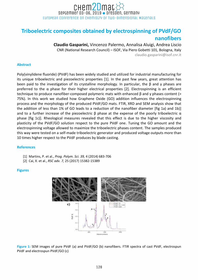
Triboelectric composites obtained by electrospinning of PVdF/GO nanofibers
Claudio Gasparini, Vincenzo Palermo, Annalisa Aluigi, Andrea Liscio CNR (National Research Council) – ISOF, Via Piero Gobetti 101, Bologna, Italy
[email protected] Abstract Poly(vinylidene fluoride) (PVdF) has been widely studied and utilized for industrial manufacturing for its unique triboelectric and piezoelectric properties [1]. In the past few years, great attention has been paid to the investigation of its crystalline morphology. In particular, the β and γ phases are preferred to the α phase for their higher electrical properties [2]. Electrospinning is an efficient technique to produce nanofiber-composed polymeric mats with enhanced β and γ phases content (> 75%). In this work we studied how Graphene Oxide (GO) addition influences the electrospinning process and the morphology of the produced PVdF/GO mats. FTIR, XRD and SEM analysis show that the addition of less than 1% of GO leads to a reduction of the nanofiber diameter [fig 1a) and 1b)] and to a further increase of the piezoelectric β phase at the expense of the poorly triboelectric α phase [fig 1c)]. Rheological measures revealed that this effect is due to the higher viscosity and plasticity of the PVdF/GO solution respect to the pure PVdF one. Tuning the GO amount and the electrospinning voltage allowed to maximize the triboelectric phases content. The samples produced this way were tested on a self-made triboelectric generator and produced voltage outputs more than 10 times higher respect to the PVdF produces by blade casting. References
[1] Martins, P. et al., Prog. Polym. Sci. 39, 4 (2014) 683-706 [2] Cai, X. et al., RSC adv. 7, 25 (2017) 15382-15389
Figures
Figure 1: SEM images of pure PVdF (a) and PVdF/GO (b) nanofibers. FTIR spectra of cast PVdF, electrospun PVdF and electrospun PVdF/GO (c)
128
MoS 2 monolayers under cluster ion irradiation : A molecular dynamics study
Sadegh Ghaderzadeh, Vladimir Ladygin, Mahdi Ghorbani-Asl, Arkady Krasheninnikov Institute of Ion Beam Physics and Materials Research, Helmholtz-Zentrum Dresden-Rossendorf,
01328 Dresden, Germany
Focused ion beams (FIB) have opened a new door on manipulation of low-dimensional materials and are sought to be particularly promising for patterning two-dimensional (2D) materials through tuning the energy, type, charge state of the incident particles and the supporting substrate [1,2,3]. This tool is recently employed to tackle the important issue of controlled pore creation in 2D materials to be performed as filters for water desalination, gas sensing, etc. This aim requires a clear insight into the microscopic process which is yet to be fully understood. In this work, we use classical Molecular Dynamics (MD) simulations to shed light on the behavior of 2D materials under cluster ion irradiation, and specifically focus on the production and characterization of defects. To a great extent, the properties of the induced defects depend on the size and energy of the clusters, which to our knowledge, has not been studied to irradiate beyond graphene so far [4]. In particular, we are focused on the response of MoS2 monolayers, which have shown various exciting properties complementary to graphene, under cluster irradiation. Furthermore, we show that depending on the incident angle and energy of the clusters, sulfur atoms can be sputtered mainly from the top layer, creating unique opportunities for patterning MoS2 monolayers. References [1] Ghorbani-Asl, Mahdi, et al. "Two-dimensional MoS2 under ion irradiation: from controlled defect production to electronic structure engineering." 2D Materials 4.2 (2017): 025078. [2] Kozubek, Roland, et al. "Perforating Freestanding Molybdenum Disulfide Monolayers with Highly Charged Ions." The journal of physical chemistry letters 10.5 (2019): 904-910. [3] Kretschmer, Silvan, et al. "Supported two-dimensional materials under ion irradiation: The substrate governs defect production." ACS applied materials & interfaces 10.36 (2018): 30827-30836. [4] Zhao, Shijun, et al. "Drilling nanopores in graphene with clusters: A molecular dynamics study." The Journal of Physical Chemistry C 116.21 (2012): 11776-11782.
129
EL ECTROCHEM ICA L MO DIF ICAT ION O F GRA PHEN E WITH MER C URY
Tobias Grosser1, M. Wehrhold1, K. Balasubramanian1 1Humboldt-Universität zu Berlin, Unter den Linden 6, 10117 Berlin, Germany
Graphene is a single sheet of sp2-hybridized carbon with outstanding physical and chemical properties such as excellent electron mobility. [1] Graphene has been investigated as an active material for numerous applications, such as electrodes in sensors and lithium-ion-batteries. [2,3] The application as sensor electrode for analytes with standard electrode potential (E0) below -0.8 V is limited due to the cathodic hydrogen evolution reaction. Mercury is still the electrode material of choice for such analytes due to its high overpotential for hydrogen evolution. [4] To combine the electrochemical properties of graphene and mercury, we modified the graphene surface through electrochemical deposition of mercury. We focused on optimizing the mercury deposition conditions and surface characterization via Atomic Force Microscopy (AFM), Electron Microscopy (SEM) and X-ray spectroscopic analysis (EDX). Subsequently, the shift of the cathodic hydrogen evolution was investigated. As an example of the performance of the mercury modified graphene electrode, we present the successful reduction of a nickel coordination complex using Square wave voltammetry (SWV). References
[1] K. S. Novoselov et al., Science, 5696 (2004), 666-669. [2] C. I. L. Justinoa, A. R. Gomes, A. C. Freitas, A. C. Duarte, T. A. P. Rocha-Santos, TrAC, 91 (2017), 53-66. [3] J. Hou, Y. Shao, M. W. Ellis, R. B. Moored, B. Yi, Phys. Chem. Chem. Phys., 34 (2011), 15384–15402. [4] D. Marin, F. Medicuti, C. Teijeiro, J. Chem. Educ., 11 (1994), A277 – A278.
130
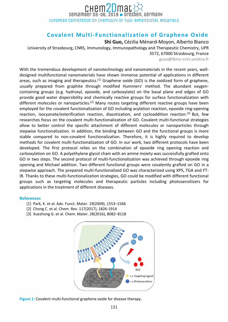
Covalent Multi -Functionalization of Graphene Oxide Shi Guo, Cécilia Ménard-Moyon, Alberto Bianco
University of Strasbourg, CNRS, Immunology, Immunopathology and Therapeutic Chemistry, UPR 3572, 67000 Strasbourg, France
With the tremendous development of nanotechnology and nanomaterials in the recent years, well-designed multifunctional nanomaterials have shown immense potential of applications in different areas, such as imaging and therapeutics.[1] Graphene oxide (GO) is the oxidized form of graphene, usually prepared from graphite through modified Hummers’ method. The abundant oxygen-containing groups (e.g. hydroxyl, epoxide, and carboxylate) on the basal plane and edges of GO provide good water dispersibility and chemically reactive groups for surface functionalization with different molecules or nanoparticles.[2] Many routes targeting different reactive groups have been employed for the covalent functionalization of GO including acylation reaction, epoxide ring-opening reaction, isocyanate/esterification reaction, diazotization, and cycloaddition reaction.[3] But, few researches focus on the covalent multi-functionalization of GO. Covalent multi-functional strategies allow to better control the specific attachment of different molecules or nanoparticles through stepwise functionalization. In addition, the binding between GO and the functional groups is more stable compared to non-covalent functionalization. Therefore, it is highly required to develop methods for covalent multi-functionalization of GO. In our work, two different protocols have been developed. The first protocol relies on the combination of epoxide ring opening reaction and carboxylation on GO. A polyethylene glycol chain with an amine moiety was successfully grafted onto GO in two steps. The second protocol of multi-functionalization was achieved through epoxide ring opening and Michael addition. Two different functional groups were covalently grafted on GO in a stepwise approach. The prepared multi-functionalized GO was characterized using XPS, TGA and FT-IR. Thanks to these multi-functionalization strategies, GO could be modified with different functional groups such as targeting molecules and therapeutic particles including photosensitizers for applications in the treatment of different diseases. References
[1] Park, K. et al. Adv. Funct. Mater. 19(2009), 1553–1566 [2] Chong C. et al. Chem. Rev. 117(2017), 1826-1914 [3] Xuezhong G. et al. Chem. Mater. 28(2016), 8082−8118
Figure 1: Covalent multi-functional graphene oxide for disease therapy.
131
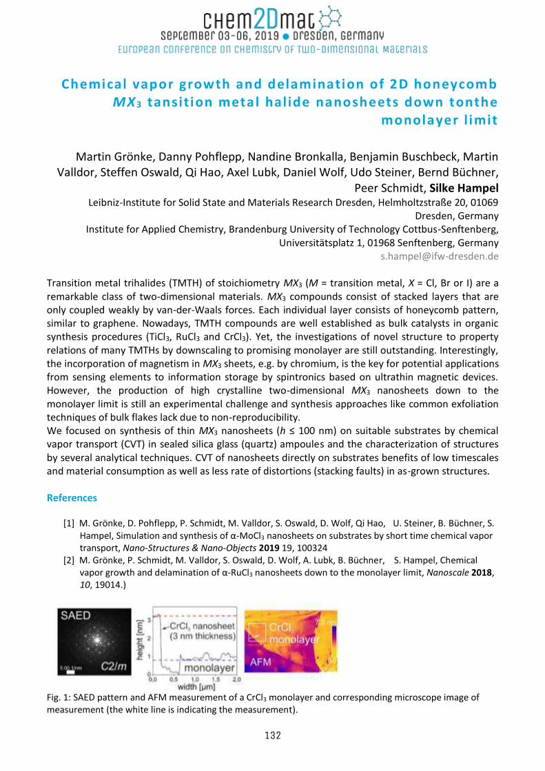
Chemical vapor growth and delamination of 2D honeycomb MX3 tansit ion metal hal ide nanosheets down tonthe
monolayer l imit
Martin Grönke, Danny Pohflepp, Nandine Bronkalla, Benjamin Buschbeck, Martin
Valldor, Steffen Oswald, Qi Hao, Axel Lubk, Daniel Wolf, Udo Steiner, Bernd Büchner, Peer Schmidt, Silke Hampel
Leibniz-Institute for Solid State and Materials Research Dresden, Helmholtzstraße 20, 01069 Dresden, Germany
Institute for Applied Chemistry, Brandenburg University of Technology Cottbus-Senftenberg, Universitätsplatz 1, 01968 Senftenberg, Germany
[email protected] Transition metal trihalides (TMTH) of stoichiometry MX3 (M = transition metal, X = Cl, Br or I) are a remarkable class of two-dimensional materials. MX3 compounds consist of stacked layers that are only coupled weakly by van-der-Waals forces. Each individual layer consists of honeycomb pattern, similar to graphene. Nowadays, TMTH compounds are well established as bulk catalysts in organic synthesis procedures (TiCl3, RuCl3 and CrCl3). Yet, the investigations of novel structure to property relations of many TMTHs by downscaling to promising monolayer are still outstanding. Interestingly, the incorporation of magnetism in MX3 sheets, e.g. by chromium, is the key for potential applications from sensing elements to information storage by spintronics based on ultrathin magnetic devices. However, the production of high crystalline two-dimensional MX3 nanosheets down to the monolayer limit is still an experimental challenge and synthesis approaches like common exfoliation techniques of bulk flakes lack due to non-reproducibility. We focused on synthesis of thin MX3 nanosheets (h ≤ 100 nm) on suitable substrates by chemical vapor transport (CVT) in sealed silica glass (quartz) ampoules and the characterization of structures by several analytical techniques. CVT of nanosheets directly on substrates benefits of low timescales and material consumption as well as less rate of distortions (stacking faults) in as-grown structures. References
[1] M. Grönke, D. Pohflepp, P. Schmidt, M. Valldor, S. Oswald, D. Wolf, Qi Hao, U. Steiner, B. Büchner, S. Hampel, Simulation and synthesis of α-MoCl3 nanosheets on substrates by short time chemical vapor transport, Nano-Structures & Nano-Objects 2019 19, 100324
[2] M. Grönke, P. Schmidt, M. Valldor, S. Oswald, D. Wolf, A. Lubk, B. Büchner, S. Hampel, Chemical vapor growth and delamination of α-RuCl3 nanosheets down to the monolayer limit, Nanoscale 2018, 10, 19014.)
Fig. 1: SAED pattern and AFM measurement of a CrCl3 monolayer and corresponding microscope image of measurement (the white line is indicating the measurement).
132
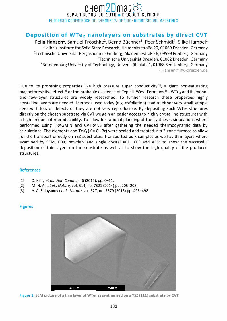
Deposition of WTe 2 nanolayers on substrates by direct CVT Felix Hansen1, Samuel Fröschke2, Bernd Büchner3, Peer Schmidt4, Silke Hampel1
1Leibniz Institute for Solid State Research, Helmholtzstraße 20, 01069 Dresden, Germany 2Technische Universität Bergakademie Freiberg, Akademiestraße 6, 09599 Freiberg, Germany
3Technische Universität Dresden, 01062 Dresden, Germany 4Brandenburg University of Technology, Universitätsplatz 1, 01968 Senftenberg, Germany
Due to its promising properties like high pressure super conductivity[1], a giant non-saturating magnetoresistive effect[2] or the probable existence of Type-II-Weyl-Fermions [3], WTe2 and its mono- and few-layer structures are widely researched. To further research these properties highly crystalline layers are needed. Methods used today (e.g. exfoliation) lead to either very small sample sizes with lots of defects or they are not very reproducible. By depositing such WTe2 structures directly on the chosen substrate via CVT we gain an easier access to highly crystalline structures with a high amount of reproducibility. To allow for rational planning of the synthesis, simulations where performed using TRAGMIN and CVTRANS after gathering the needed thermodynamic data by calculations. The elements and TeX4 (X = Cl, Br) were sealed and treated in a 2-zone-furnace to allow for the transport directly on YSZ substrates. Transported bulk samples as well as thin layers where examined by SEM, EDX, powder- and single crystal XRD, XPS and AFM to show the successful deposition of thin layers on the substrate as well as to show the high quality of the produced structures. References [1] D. Kang et al., Nat. Commun. 6 (2015), pp. 6–11. [2] M. N. Ali et al., Nature, vol. 514, no. 7521 (2014) pp. 205–208. [3] A. A. Soluyanov et al., Nature, vol. 527, no. 7579 (2015) pp. 495–498.
Figures
Figure 1: SEM picture of a thin layer of WTe2 as synthesized on a YSZ (111) substrate by CVT
133
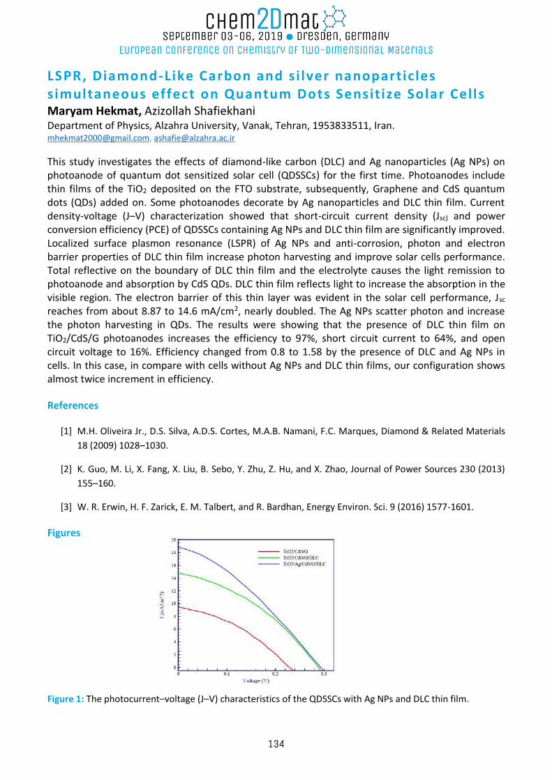
LSPR, Diamond-Like Carbon and s i lver nanoparticles s imultaneous effect on Quantum Dots Sensitize Solar Cel ls Maryam Hekmat, Azizollah Shafiekhani Department of Physics, Alzahra University, Vanak, Tehran, 1953833511, Iran. [email protected], [email protected]
This study investigates the effects of diamond-like carbon (DLC) and Ag nanoparticles (Ag NPs) on photoanode of quantum dot sensitized solar cell (QDSSCs) for the first time. Photoanodes include thin films of the TiO2 deposited on the FTO substrate, subsequently, Graphene and CdS quantum dots (QDs) added on. Some photoanodes decorate by Ag nanoparticles and DLC thin film. Current density-voltage (J–V) characterization showed that short-circuit current density (Jsc) and power conversion efficiency (PCE) of QDSSCs containing Ag NPs and DLC thin film are significantly improved. Localized surface plasmon resonance (LSPR) of Ag NPs and anti-corrosion, photon and electron barrier properties of DLC thin film increase photon harvesting and improve solar cells performance. Total reflective on the boundary of DLC thin film and the electrolyte causes the light remission to photoanode and absorption by CdS QDs. DLC thin film reflects light to increase the absorption in the visible region. The electron barrier of this thin layer was evident in the solar cell performance, Jsc reaches from about 8.87 to 14.6 mA/cm2, nearly doubled. The Ag NPs scatter photon and increase the photon harvesting in QDs. The results were showing that the presence of DLC thin film on TiO2/CdS/G photoanodes increases the efficiency to 97%, short circuit current to 64%, and open circuit voltage to 16%. Efficiency changed from 0.8 to 1.58 by the presence of DLC and Ag NPs in cells. In this case, in compare with cells without Ag NPs and DLC thin films, our configuration shows almost twice increment in efficiency. References
[1] M.H. Oliveira Jr., D.S. Silva, A.D.S. Cortes, M.A.B. Namani, F.C. Marques, Diamond & Related Materials
18 (2009) 1028–1030.
[2] K. Guo, M. Li, X. Fang, X. Liu, B. Sebo, Y. Zhu, Z. Hu, and X. Zhao, Journal of Power Sources 230 (2013)
155–160.
[3] W. R. Erwin, H. F. Zarick, E. M. Talbert, and R. Bardhan, Energy Environ. Sci. 9 (2016) 1577-1601.
Figures
Figure 1: The photocurrent–voltage (J–V) characteristics of the QDSSCs with Ag NPs and DLC thin film.
134
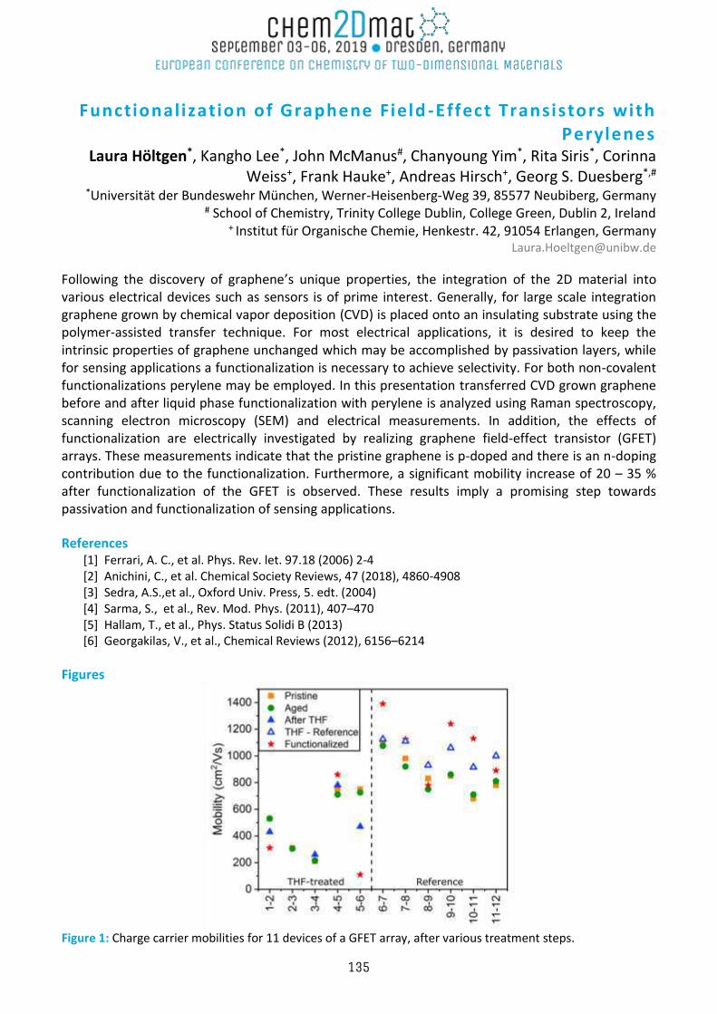
Functionalization of Graphene Field -Effect Transistors with Perylenes
Laura Höltgen*, Kangho Lee*, John McManus#, Chanyoung Yim*, Rita Siris*, Corinna Weiss+, Frank Hauke+, Andreas Hirsch+, Georg S. Duesberg*,#
*Universität der Bundeswehr München, Werner-Heisenberg-Weg 39, 85577 Neubiberg, Germany # School of Chemistry, Trinity College Dublin, College Green, Dublin 2, Ireland
+ Institut für Organische Chemie, Henkestr. 42, 91054 Erlangen, Germany [email protected]
Following the discovery of graphene’s unique properties, the integration of the 2D material into various electrical devices such as sensors is of prime interest. Generally, for large scale integration graphene grown by chemical vapor deposition (CVD) is placed onto an insulating substrate using the polymer-assisted transfer technique. For most electrical applications, it is desired to keep the intrinsic properties of graphene unchanged which may be accomplished by passivation layers, while for sensing applications a functionalization is necessary to achieve selectivity. For both non-covalent functionalizations perylene may be employed. In this presentation transferred CVD grown graphene before and after liquid phase functionalization with perylene is analyzed using Raman spectroscopy, scanning electron microscopy (SEM) and electrical measurements. In addition, the effects of functionalization are electrically investigated by realizing graphene field-effect transistor (GFET) arrays. These measurements indicate that the pristine graphene is p-doped and there is an n-doping contribution due to the functionalization. Furthermore, a significant mobility increase of 20 – 35 % after functionalization of the GFET is observed. These results imply a promising step towards passivation and functionalization of sensing applications.
References [1] Ferrari, A. C., et al. Phys. Rev. let. 97.18 (2006) 2-4 [2] Anichini, C., et al. Chemical Society Reviews, 47 (2018), 4860-4908 [3] Sedra, A.S.,et al., Oxford Univ. Press, 5. edt. (2004) [4] Sarma, S., et al., Rev. Mod. Phys. (2011), 407–470 [5] Hallam, T., et al., Phys. Status Solidi B (2013) [6] Georgakilas, V., et al., Chemical Reviews (2012), 6156–6214
Figures
Figure 1: Charge carrier mobilities for 11 devices of a GFET array, after various treatment steps.
135
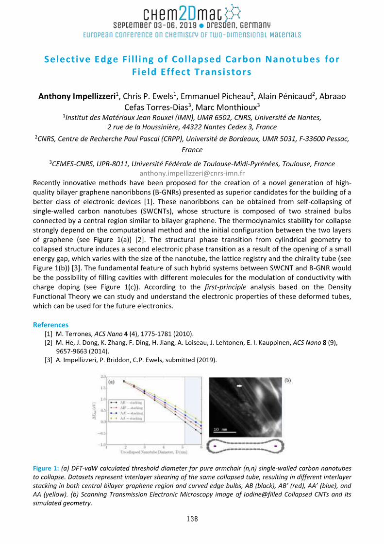
Selective Edge Fi l l ing of Collapsed Carbon Nanotubes for F ield Effect Transistors
Anthony Impellizzeri1, Chris P. Ewels1, Emmanuel Picheau2, Alain Pénicaud2, Abraao
Cefas Torres-Dias3, Marc Monthioux3
1Institut des Matériaux Jean Rouxel (IMN), UMR 6502, CNRS, Université de Nantes, 2 rue de la Houssinière, 44322 Nantes Cedex 3, France
2CNRS, Centre de Recherche Paul Pascal (CRPP), Université de Bordeaux, UMR 5031, F-33600 Pessac,
France
3CEMES-CNRS, UPR-8011, Université Fédérale de Toulouse-Midi-Pyrénées, Toulouse, France [email protected]
Recently innovative methods have been proposed for the creation of a novel generation of high-quality bilayer graphene nanoribbons (B-GNRs) presented as superior candidates for the building of a better class of electronic devices [1]. These nanoribbons can be obtained from self-collapsing of single-walled carbon nanotubes (SWCNTs), whose structure is composed of two strained bulbs connected by a central region similar to bilayer graphene. The thermodynamics stability for collapse strongly depend on the computational method and the initial configuration between the two layers of graphene (see Figure 1(a)) [2]. The structural phase transition from cylindrical geometry to collapsed structure induces a second electronic phase transition as a result of the opening of a small energy gap, which varies with the size of the nanotube, the lattice registry and the chirality tube (see Figure 1(b)) [3]. The fundamental feature of such hybrid systems between SWCNT and B-GNR would be the possibility of filling cavities with different molecules for the modulation of conductivity with charge doping (see Figure 1(c)). According to the first-principle analysis based on the Density Functional Theory we can study and understand the electronic properties of these deformed tubes, which can be used for the future electronics. References
[1] M. Terrones, ACS Nano 4 (4), 1775-1781 (2010). [2] M. He, J. Dong, K. Zhang, F. Ding, H. Jiang, A. Loiseau, J. Lehtonen, E. I. Kauppinen, ACS Nano 8 (9),
9657-9663 (2014). [3] A. Impellizzeri, P. Briddon, C.P. Ewels, submitted (2019).
Figure 1: (a) DFT-vdW calculated threshold diameter for pure armchair (n,n) single-walled carbon nanotubes to collapse. Datasets represent interlayer shearing of the same collapsed tube, resulting in different interlayer stacking in both central bilayer graphene region and curved edge bulbs, AB (black), AB’ (red), AA’ (blue), and AA (yellow). (b) Scanning Transmission Electronic Microscopy image of Iodine@filled Collapsed CNTs and its simulated geometry.
136
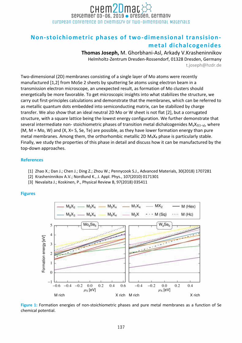
Non-stoichiometric phases of two -dimensional transision -metal dichalcogenides
Thomas Joseph, M. Ghorbhani-Asl, Arkady V.Krasheninnikov
Helmholtz-Zentrum Dresden-Rossendorf, 01328 Dresden, Germany
Two-dimensional (2D) membranes consisting of a single layer of Mo atoms were recently manufactured [1,2] from MoSe 2 sheets by sputtering Se atoms using electron beam in a transmission electron microscope, an unexpected result, as formation of Mo clusters should energetically be more favorable. To get microscopic insights into what stabilizes the structure, we carry out first-principles calculations and demonstrate that the membranes, which can be referred to as metallic quantum dots embedded into semiconducting matrix, can be stabilized by charge transfer. We also show that an ideal neutral 2D Mo or W sheet is not flat [2], but a corrugated structure, with a square lattice being the lowest energy configuration. We further demonstrate that several intermediate non- stoichiometric phases of transition metal dichalcogenides MyX2(1−y), where (M, M = Mo, W) and (X, X= S, Se, Te) are possible, as they have lower formation energy than pure metal membranes. Among them, the orthorhombic metallic 2D M4X4 phase is particularly stable. Finally, we study the properties of this phase in detail and discuss how it can be manufactured by the top-down approaches.
References
[1] Zhao X.; Dan J.; Chen J.; Ding Z.; Zhou W.; Pennycook S.J., Advanced Materials, 30(2018) 1707281 [2] Krasheninnikov A.V.; Nordlund K., J. Appl. Phys., 107(2010) 0171301 [3] Nevalaita J.; Koskinen, P., Physical Review B, 97(2018) 035411
Figures
Figure 1: Formation energies of non-stoichiometric phases and pure metal membranes as a function of Se chemical potential.
137
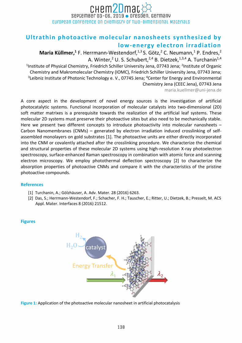
Ultrathin photoactive molecular nanosheets synthesized by low-energy electron i rradiation
Maria Küllmer,1 F. Herrmann-Westendorf,1,3 S. Götz,2 C. Neumann,1 P. Endres,2 A. Winter,2 U. S. Schubert,2,4 B. Dietzek,1,3,4 A. Turchanin1,4
1Institute of Physical Chemistry, Friedrich Schiller University Jena, 07743 Jena; 2Institute of Organic Chemistry and Makromolecular Chemistry (IOMC), Friedrich Schiller University Jena, 07743 Jena;
3Leibniz Institute of Photonic Technology e. V., 07745 Jena; 4Center for Energy and Environmental Chemistry Jena (CEEC Jena), 07743 Jena
A core aspect in the development of novel energy sources is the investigation of artificial photocatalytic systems. Functional incorporation of molecular catalysts into two-dimensional (2D) soft matter matrixes is a prerequisite towards the realization of the artificial leaf systems. These molecular 2D systems must preserve their photoactive sites but also need to be mechanically stable. Here we present two different concepts to introduce photoactivity into molecular nanosheets – Carbon Nanomembranes (CNMs) – generated by electron irradiation induced crosslinking of self-assembled monolayers on gold substrates [1]. The photoactive units are either directly incorporated into the CNM or covalently attached after the crosslinking procedure. We characterize the chemical and structural properties of these molecular 2D systems using high-resolution X-ray photoelectron spectroscopy, surface-enhanced Raman spectroscopy in combination with atomic force and scanning electron microscopy. We employ photothermal deflection spectroscopy [2] to characterize the absorption properties of photoactive CNMs and compare it with the characteristics of the pristine photoactive compounds. References
[1] Turchanin, A.; Gölzhäuser, A. Adv. Mater. 28 (2016) 6263. [2] Das, S.; Herrmann-Westendorf, F.; Schacher, F. H.; Tauscher, E.; Ritter, U.; Dietzek, B.; Presselt, M. ACS
Appl. Mater. Interfaces 8 (2016) 21512.
Figures
Figure 1: Application of the photoactive molecular nanosheet in artificial photocatalysis
CNM
catalyst
Energy Transfer
138
Liquid-gated transistors based on reduced graphene oxide for sensing and biosensing
Pietro Antonio Livio, Stefano Casalini, Rafael Furlan De Oliveira, Verónica Montes-García, Paolo Samorì
Université de Strasbourg, CNRS, ISIS UMR 7006, 8 allée Gaspard Monge, F-67000 Strasbourg, France [email protected]
Liquid-gated transistors (LGTs) have been recognized as powerful electrical transducers of physical, chemical and biochemical events due to their unique characteristics, such as high sensitivity, signal amplification ability, multi-parametricity, inherent operation in water, and low working voltages [1]. Traditionally, organic semiconductors and conducting polymers have been employed as the active thin-film materials in LGTs. The use of reduced graphene oxide (rGO), however, offers several additional characteristics to LGT sensors and biosensors, namely ultrathin thickness, flexibility, elevated conductivity, low-cost and green (water-based) processing. The main advantage of rGO though lies on its rich chemical functionality endowed by oxygen groups (-OH, -COOH, -COC-) that allows one to tether (bio)molecules on the device while preserving the rGO elevated conductivity [2]. Thus, LGT sensors and biosensors based on functionalized rGO films can be developed for one or more targeted analytes. Here we present a robust, all-green, and industrial scalable fabrication of rGO LGTs for sensing and biosensing. Rigid and flexible rGO devices have been fabricated and functionalized with chemical and biochemical species. The first route exploits the direct covalent binding of amino-terminated crown-ether molecules on the GO basal plane through the ring opening reaction of its epoxide groups. The functionalized GO is therefore electrochemically reduced to produce functional rGO LGTs for the detection of metal cations in solution. For this purpose, two derived strategies have been studied, the in-situ GO functionalization (in solution) and the ex-situ one (as a film). The second application relies on the biochemical functionalization of rGO LGTs also by epoxide ring opening reactions to attach LupuzorTM – a biological drug for the treatment of systemic Lupus [3]. For both chemical and biochemical functionalization strategies, the GO and rGO structural, morphological and electrical properties in LGT configuration have been detailed investigated. This work aims to gain deeper insights on realistic development of commercial sensors and biosensors based on functionalized 2D materials. References
[1] Kergoat, L.; Herlogsson, L.; Braga, D.; Piro, B.; Pham, M.-C.; Crispin, X.; Berggren, M.; Horowitz, G. A Water-Gate Organic Field-Effect Transistor. Adv. Mater. 2010, 22 (23), 2565–2569.
[2] Xu, J.; Wang, Y.; Hu, S. Nanocomposites of Graphene and Graphene Oxides: Synthesis, Molecular Functionalization and Application in Electrochemical Sensors and Biosensors. A Review. Microchimica Acta 2017, 184 (1), 1–44.
[3] Zimmer, R.; Scherbarth, H. R.; Rillo, O. L.; Gomez-Reino, J. J.; Muller, S. Lupuzor/P140 Peptide in Patients with Systemic Lupus Erythematosus: A Randomised, Double-Blind, Placebo-Controlled Phase IIb Clinical Trial. Ann Rheum Dis 2013, 72 (11), 1830–1835.
139
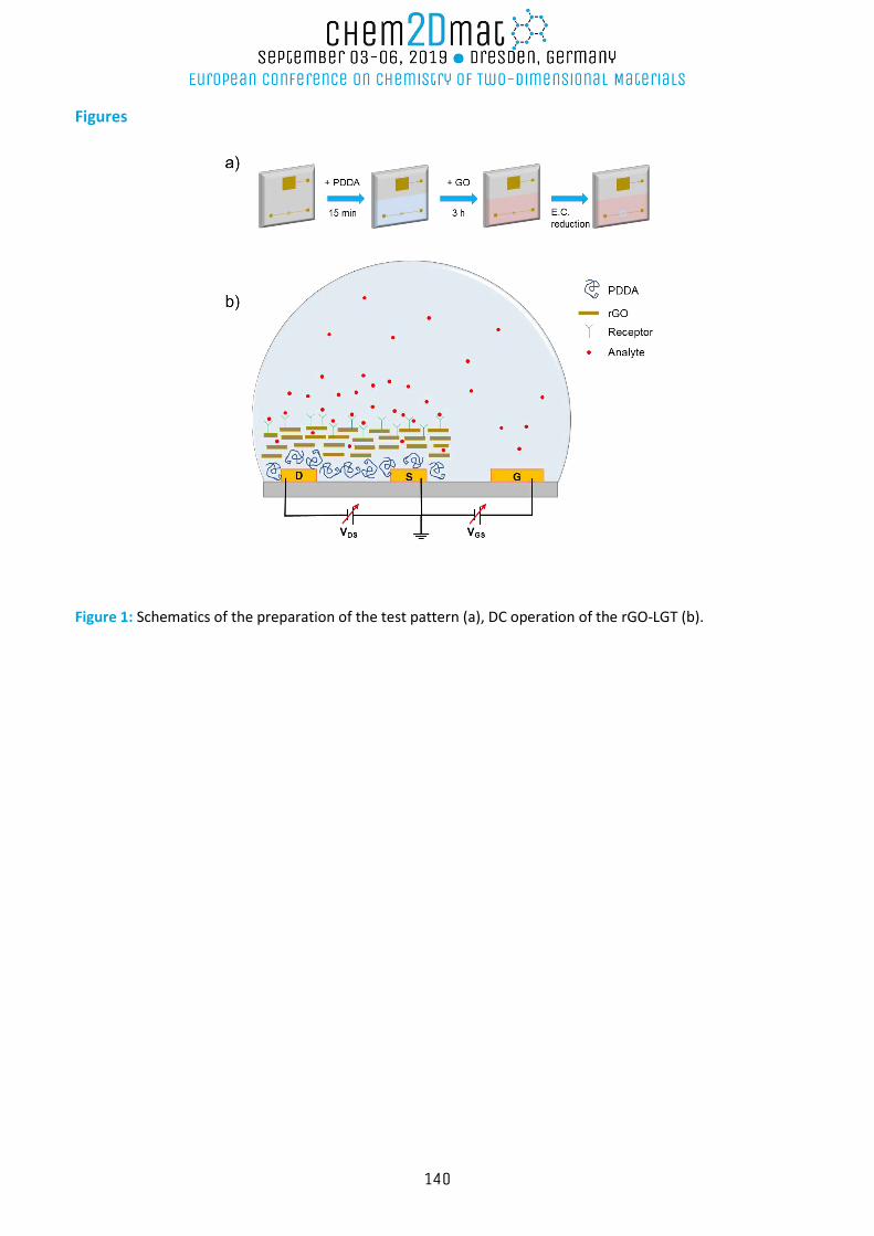
Figures
Figure 1: Schematics of the preparation of the test pattern (a), DC operation of the rGO-LGT (b).
140
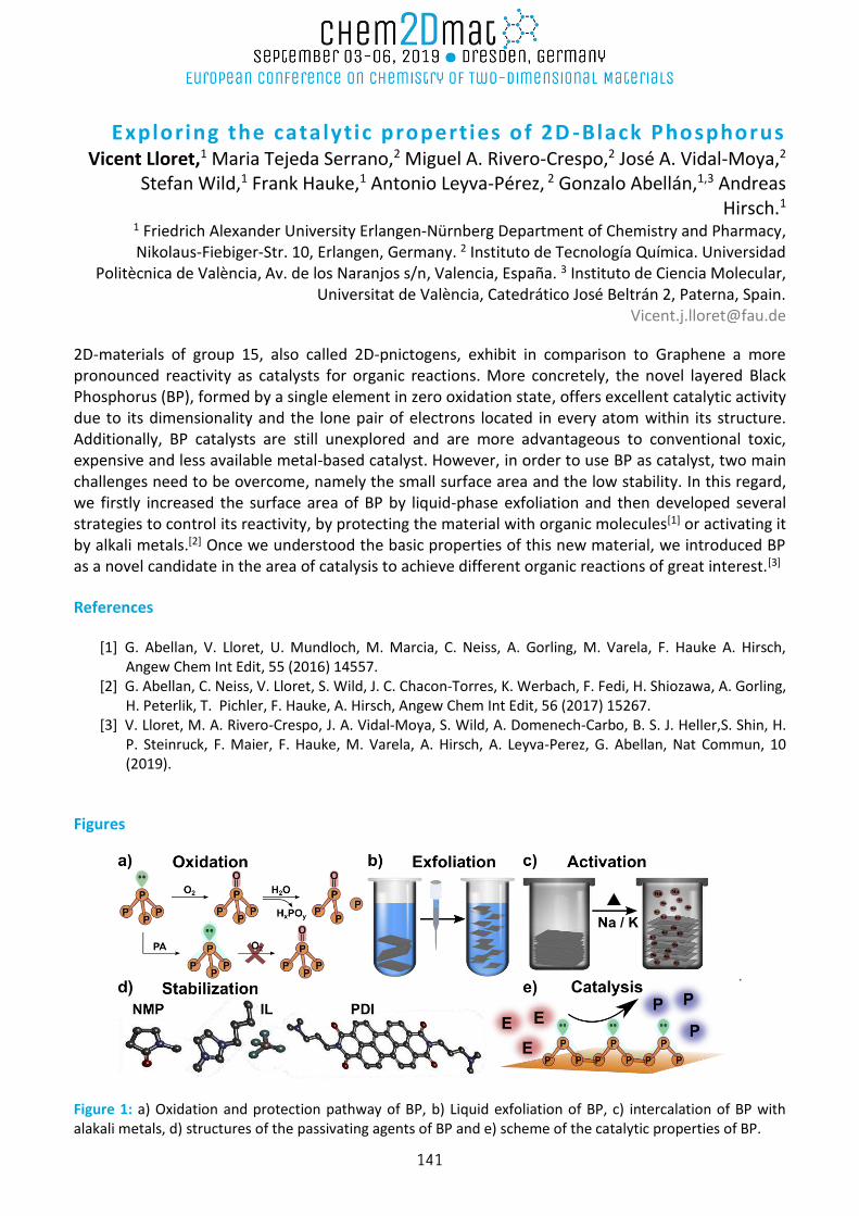
Exploring the catalytic propert ies of 2D -Black Phosphorus Vicent Lloret,1 Maria Tejeda Serrano,2 Miguel A. Rivero-Crespo,2 José A. Vidal-Moya,2
Stefan Wild,1 Frank Hauke,1 Antonio Leyva-Pérez, 2 Gonzalo Abellán,1,3 Andreas Hirsch.1
1 Friedrich Alexander University Erlangen-Nürnberg Department of Chemistry and Pharmacy, Nikolaus-Fiebiger-Str. 10, Erlangen, Germany. 2 Instituto de Tecnología Química. Universidad
Politècnica de València, Av. de los Naranjos s/n, Valencia, España. 3 Instituto de Ciencia Molecular, Universitat de València, Catedrático José Beltrán 2, Paterna, Spain.
2D-materials of group 15, also called 2D-pnictogens, exhibit in comparison to Graphene a more pronounced reactivity as catalysts for organic reactions. More concretely, the novel layered Black Phosphorus (BP), formed by a single element in zero oxidation state, offers excellent catalytic activity due to its dimensionality and the lone pair of electrons located in every atom within its structure. Additionally, BP catalysts are still unexplored and are more advantageous to conventional toxic, expensive and less available metal-based catalyst. However, in order to use BP as catalyst, two main challenges need to be overcome, namely the small surface area and the low stability. In this regard, we firstly increased the surface area of BP by liquid-phase exfoliation and then developed several strategies to control its reactivity, by protecting the material with organic molecules[1] or activating it by alkali metals.[2] Once we understood the basic properties of this new material, we introduced BP as a novel candidate in the area of catalysis to achieve different organic reactions of great interest.[3] References
[1] G. Abellan, V. Lloret, U. Mundloch, M. Marcia, C. Neiss, A. Gorling, M. Varela, F. Hauke A. Hirsch, Angew Chem Int Edit, 55 (2016) 14557.
[2] G. Abellan, C. Neiss, V. Lloret, S. Wild, J. C. Chacon-Torres, K. Werbach, F. Fedi, H. Shiozawa, A. Gorling, H. Peterlik, T. Pichler, F. Hauke, A. Hirsch, Angew Chem Int Edit, 56 (2017) 15267.
[3] V. Lloret, M. A. Rivero-Crespo, J. A. Vidal-Moya, S. Wild, A. Domenech-Carbo, B. S. J. Heller,S. Shin, H. P. Steinruck, F. Maier, F. Hauke, M. Varela, A. Hirsch, A. Leyva-Perez, G. Abellan, Nat Commun, 10 (2019).
Figures
Figure 1: a) Oxidation and protection pathway of BP, b) Liquid exfoliation of BP, c) intercalation of BP with alakali metals, d) structures of the passivating agents of BP and e) scheme of the catalytic properties of BP.
141
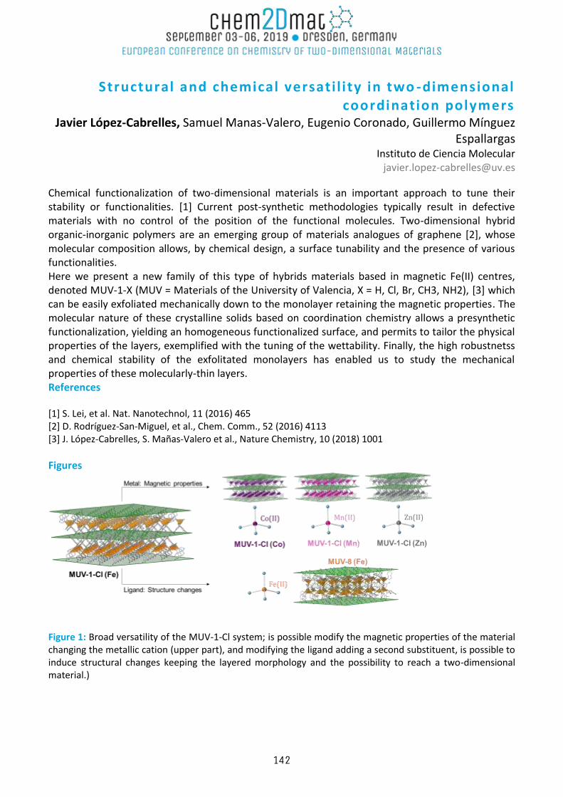
Structural and chemical versati l i ty in two -dimensional coordination polymers
Javier López-Cabrelles, Samuel Manas-Valero, Eugenio Coronado, Guillermo Mínguez Espallargas
Instituto de Ciencia Molecular [email protected]
Chemical functionalization of two-dimensional materials is an important approach to tune their stability or functionalities. [1] Current post-synthetic methodologies typically result in defective materials with no control of the position of the functional molecules. Two-dimensional hybrid organic-inorganic polymers are an emerging group of materials analogues of graphene [2], whose molecular composition allows, by chemical design, a surface tunability and the presence of various functionalities. Here we present a new family of this type of hybrids materials based in magnetic Fe(II) centres, denoted MUV-1-X (MUV = Materials of the University of Valencia, X = H, Cl, Br, CH3, NH2), [3] which can be easily exfoliated mechanically down to the monolayer retaining the magnetic properties. The molecular nature of these crystalline solids based on coordination chemistry allows a presynthetic functionalization, yielding an homogeneous functionalized surface, and permits to tailor the physical properties of the layers, exemplified with the tuning of the wettability. Finally, the high robustnetss and chemical stability of the exfolitated monolayers has enabled us to study the mechanical properties of these molecularly-thin layers. References [1] S. Lei, et al. Nat. Nanotechnol, 11 (2016) 465 [2] D. Rodríguez-San-Miguel, et al., Chem. Comm., 52 (2016) 4113 [3] J. López-Cabrelles, S. Mañas-Valero et al., Nature Chemistry, 10 (2018) 1001
Figures
Figure 1: Broad versatility of the MUV-1-Cl system; is possible modify the magnetic properties of the material changing the metallic cation (upper part), and modifying the ligand adding a second substituent, is possible to induce structural changes keeping the layered morphology and the possibility to reach a two-dimensional material.)
142
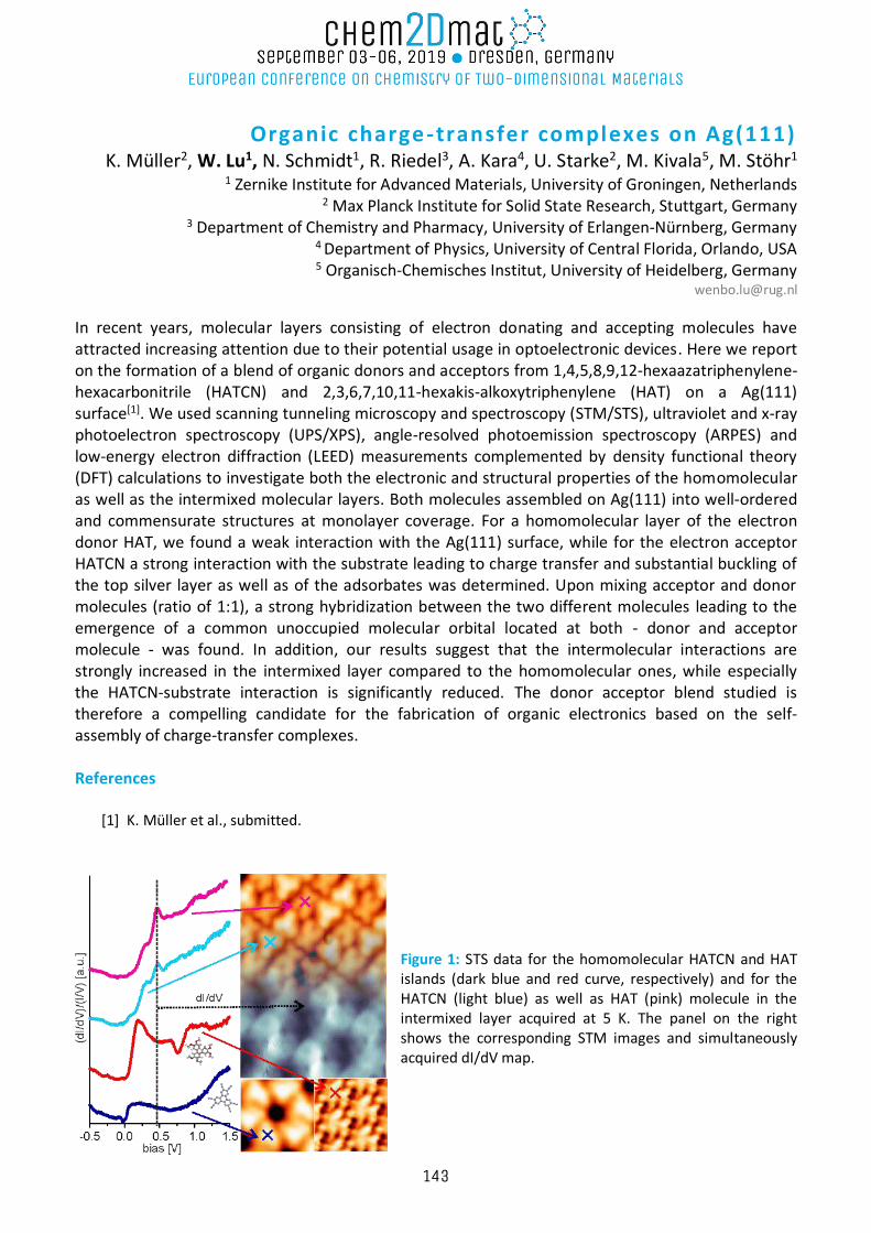
Organic charge-transfer complexes on Ag(111) K. Müller2, W. Lu1, N. Schmidt1, R. Riedel3, A. Kara4, U. Starke2, M. Kivala5, M. Stöhr1
1 Zernike Institute for Advanced Materials, University of Groningen, Netherlands 2 Max Planck Institute for Solid State Research, Stuttgart, Germany
3 Department of Chemistry and Pharmacy, University of Erlangen-Nürnberg, Germany 4 Department of Physics, University of Central Florida, Orlando, USA 5 Organisch-Chemisches Institut, University of Heidelberg, Germany
In recent years, molecular layers consisting of electron donating and accepting molecules have attracted increasing attention due to their potential usage in optoelectronic devices. Here we report on the formation of a blend of organic donors and acceptors from 1,4,5,8,9,12-hexaazatriphenylene-hexacarbonitrile (HATCN) and 2,3,6,7,10,11-hexakis-alkoxytriphenylene (HAT) on a Ag(111) surface[1]. We used scanning tunneling microscopy and spectroscopy (STM/STS), ultraviolet and x-ray photoelectron spectroscopy (UPS/XPS), angle-resolved photoemission spectroscopy (ARPES) and low-energy electron diffraction (LEED) measurements complemented by density functional theory (DFT) calculations to investigate both the electronic and structural properties of the homomolecular as well as the intermixed molecular layers. Both molecules assembled on Ag(111) into well-ordered and commensurate structures at monolayer coverage. For a homomolecular layer of the electron donor HAT, we found a weak interaction with the Ag(111) surface, while for the electron acceptor HATCN a strong interaction with the substrate leading to charge transfer and substantial buckling of the top silver layer as well as of the adsorbates was determined. Upon mixing acceptor and donor molecules (ratio of 1:1), a strong hybridization between the two different molecules leading to the emergence of a common unoccupied molecular orbital located at both - donor and acceptor molecule - was found. In addition, our results suggest that the intermolecular interactions are strongly increased in the intermixed layer compared to the homomolecular ones, while especially the HATCN-substrate interaction is significantly reduced. The donor acceptor blend studied is therefore a compelling candidate for the fabrication of organic electronics based on the self-assembly of charge-transfer complexes. References
[1] K. Müller et al., submitted.
Figure 1: STS data for the homomolecular HATCN and HAT islands (dark blue and red curve, respectively) and for the HATCN (light blue) as well as HAT (pink) molecule in the intermixed layer acquired at 5 K. The panel on the right shows the corresponding STM images and simultaneously acquired dI/dV map.
143
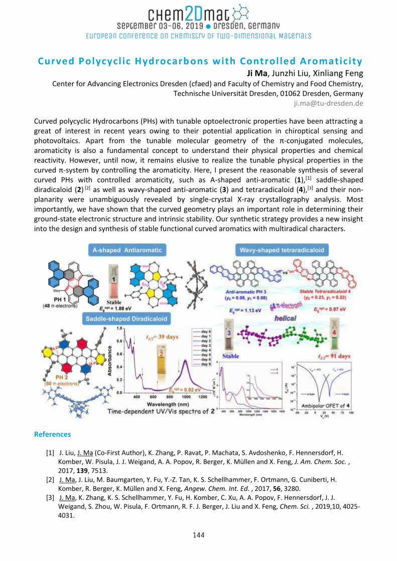
Curved Polycycl ic Hydrocarb ons with Control led Aromaticity Ji Ma, Junzhi Liu, Xinliang Feng
Center for Advancing Electronics Dresden (cfaed) and Faculty of Chemistry and Food Chemistry, Technische Universität Dresden, 01062 Dresden, Germany
Curved polycyclic Hydrocarbons (PHs) with tunable optoelectronic properties have been attracting a great of interest in recent years owing to their potential application in chiroptical sensing and photovoltaics. Apart from the tunable molecular geometry of the π-conjugated molecules, aromaticity is also a fundamental concept to understand their physical properties and chemical reactivity. However, until now, it remains elusive to realize the tunable physical properties in the curved π-system by controlling the aromaticity. Here, I present the reasonable synthesis of several curved PHs with controlled aromaticity, such as A-shaped anti-aromatic (1),[1] saddle-shaped diradicaloid (2) [2] as well as wavy-shaped anti-aromatic (3) and tetraradicaloid (4),[3] and their non-planarity were unambiguously revealed by single-crystal X-ray crystallography analysis. Most importantly, we have shown that the curved geometry plays an important role in determining their ground-state electronic structure and intrinsic stability. Our synthetic strategy provides a new insight into the design and synthesis of stable functional curved aromatics with multiradical characters.
References
[1] J. Liu, J. Ma (Co-First Author), K. Zhang, P. Ravat, P. Machata, S. Avdoshenko, F. Hennersdorf, H. Komber, W. Pisula, J. J. Weigand, A. A. Popov, R. Berger, K. Müllen and X. Feng, J. Am. Chem. Soc. , 2017, 139, 7513.
[2] J. Ma, J. Liu, M. Baumgarten, Y. Fu, Y.-Z. Tan, K. S. Schellhammer, F. Ortmann, G. Cuniberti, H. Komber, R. Berger, K. Müllen and X. Feng, Angew. Chem. Int. Ed. , 2017, 56, 3280.
[3] J. Ma, K. Zhang, K. S. Schellhammer, Y. Fu, H. Komber, C. Xu, A. A. Popov, F. Hennersdorf, J. J. Weigand, S. Zhou, W. Pisula, F. Ortmann, R. F. J. Berger, J. Liu and X. Feng, Chem. Sci. , 2019,10, 4025-4031.
144
Properties of h-BN monolayer grown on curved Ni crystal :
oxidation and oxygen intercalat ion Anna Makarova1,2*, L. Fernandez1,3, D. Yu. Usachov4, A. Fedorov5, K. A. Bokai4,
D. A. Smirnov1, C. Laubschat1, D. V. Vyalikh6,7, F. Schiller3,6, and J. E. Ortega3,6,8
1Technische Universität Dresden, Dresden, Germany 2*Physikalische Chemie, Institut für Chemie und Biochemie, Freie Universität Berlin, Berlin, Germany
3CFM-MPC, Paseo de Manuel Lardizabal 5, San Sebastian, Spain 4St. Petersburg State University, Universitetskaya Nab.7-9, St. Petersburg, Russia
5ISSR IFW-Dresden, Dresden, Germany 6Donostia International Physics Centre, Paseo de Manuel Lardizabal 4, San Sebastian, Spain
7IKERBASQUE, Basque Foundation for Science, Bilbao, Spain 8Universidad del Pas Vasco, UPV-EHU, San Sebastian, Spain
*present address
Curving crystals to expose surfaces of variable orientation is a straightforward approach to explore
appropriate templates and tunable substrates for 2D materials. It allows the systematic search and
rational determination of an optimal growth substrate. A cylindrical crystal with a high-symmetry
axis is the simplest curved geometry, but sufficient to span a full set of vicinal planes with close-
packed steps. As demonstrated repeatedly, the cylindrical geometry is easy to handle and process in
standard vacuum setups [1,2]. Moreover, it is particularly convenient for electron spectroscopies
that make use of micron-sized photon beams in synchrotrons, such as Near-Edge X-ray Absorption
and X-ray photoemission, since these can be scanned on the curved surface to smoothly probe
different vicinal planes. Recently, we investigated the growth of h-BN on a Ni surface curved around
the (111) direction [c-Ni(111)] [1]. We observed the formation of a well-defined, homogeneous h-BN
monolayer all across the curved crystal, exhibiting an increasing presence of h-BN-covered micro-
facets, as the surface plane tilted away from the (111) plane.
In the present study we systematically investigate the effect of thermal oxygen exposure of the h-BN
monolayer interfacing a full variety of vicinal orientations around the Ni(111) high-symmetry
direction [2]. Using Scanning Tunneling Microscopy, X-ray Absorption and Photoemission
Spectroscopies we demonstrate the occurrence of two processes upon oxygen exposure: oxygen
intercalation underneath the h-BN layer, which leads to decoupling of the h-BN from the substrate,
and oxidation of h-BN itself, which proceeds via substitution of nitrogen atoms
References
[1] Fernandez, L., et al. 2D Materials, 6 (2019) 025013.
[2] Makarova, A., et al. J. Phys. Chem. C, 123 (2019) 593–602.
145
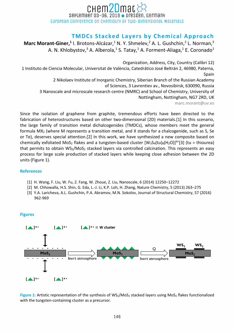
TMDCs Stacked Layers by Chemical Approach Marc Morant-Giner,1 I. Brotons-Alcázar,1 N. Y. Shmelev,2 A. L. Gushchin,2 L. Norman,3
A. N. Khlobystov,3 A. Alberola,1 S. Tatay,1 A. Forment-Aliaga,1 E. Coronado1
Organization, Address, City, Country (Calibri 12) 1 Instituto de Ciencia Molecular, Universitat de València, Catedrático José Beltrán 2, 46980, Paterna,
Spain 2 Nikolaev Institute of Inorganic Chemistry, Siberian Branch of the Russian Academy
of Sciences, 3 Lavrentiev av., Novosibirsk, 630090, Russia 3 Nanoscale and microscale research centre (NMRC) and School of Chemistry, University of
Nottingham, Nottingham, NG7 2RD, UK [email protected]
Since the isolation of graphene from graphite, tremendous efforts have been directed to the fabrication of heterostructures based on other two-dimensional (2D) materials.[1] In this scenario, the large family of transition metal dichalcogenides (TMDCs), whose members meet the general formula MX2 (where M represents a transition metal, and X stands for a chalcogenide, such as S, Se or Te), deserves special attention.[2] In this work, we have synthesized a new composite based on chemically exfoliated MoS2 flakes and a tungsten-based cluster [W3S4(tu)8(H2O)]4+[3] (tu = thiourea) that permits to obtain WS2/MoS2 stacked layers via controlled calcination. This represents an easy process for large scale production of stacked layers while keeping close adhesion between the 2D units (Figure 1). References
[1] H. Wang, F. Liu, W. Fu, Z. Fang, W. Zhoue, Z. Liu, Nanoscale, 6 (2014) 12250–12272 [2] M. Chhowalla, H.S. Shin, G. Eda, L.-J. Li, K.P. Loh, H. Zhang, Nature Chemistry, 5 (2013) 263–275 [3] Y.А. Laricheva, A.L. Gushchin, P.А. Аbramov, М.N. Sokolov, Journal of Structural Chemistry, 57 (2016)
962-969
Figures
Figure 1: Artistic representation of the synthesis of WS2/MoS2 stacked layers using MoS2 flakes functionalized with the tungsten-containing cluster as a precursor.
146
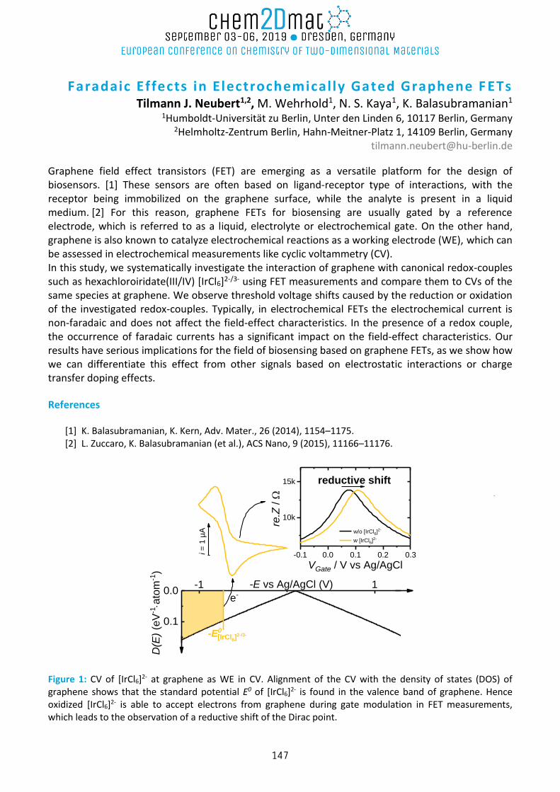
Faradaic Effects in Electrochemical ly Gated Graphene F ETs Tilmann J. Neubert1,2, M. Wehrhold1, N. S. Kaya1, K. Balasubramanian1
1Humboldt-Universität zu Berlin, Unter den Linden 6, 10117 Berlin, Germany 2Helmholtz-Zentrum Berlin, Hahn-Meitner-Platz 1, 14109 Berlin, Germany
[email protected] Graphene field effect transistors (FET) are emerging as a versatile platform for the design of biosensors. [1] These sensors are often based on ligand-receptor type of interactions, with the receptor being immobilized on the graphene surface, while the analyte is present in a liquid medium. [2] For this reason, graphene FETs for biosensing are usually gated by a reference electrode, which is referred to as a liquid, electrolyte or electrochemical gate. On the other hand, graphene is also known to catalyze electrochemical reactions as a working electrode (WE), which can be assessed in electrochemical measurements like cyclic voltammetry (CV). In this study, we systematically investigate the interaction of graphene with canonical redox-couples such as hexachloroiridate(III/IV) [IrCl6]2-/3- using FET measurements and compare them to CVs of the same species at graphene. We observe threshold voltage shifts caused by the reduction or oxidation of the investigated redox-couples. Typically, in electrochemical FETs the electrochemical current is non-faradaic and does not affect the field-effect characteristics. In the presence of a redox couple, the occurrence of faradaic currents has a significant impact on the field-effect characteristics. Our results have serious implications for the field of biosensing based on graphene FETs, as we show how we can differentiate this effect from other signals based on electrostatic interactions or charge transfer doping effects.
References
[1] K. Balasubramanian, K. Kern, Adv. Mater., 26 (2014), 1154–1175. [2] L. Zuccaro, K. Balasubramanian (et al.), ACS Nano, 9 (2015), 11166–11176.
-0.1 0.0 0.1 0.2 0.3
10k
15k
-1 1
0.1
0.0-E vs Ag/AgCl (V)
D(E
) (e
V-1a
tom
-1)
-E0[IrCl6]2-/3-
e-
i =
1 µ
A w/o [IrCl6]2-
w [IrCl6]2-
re.Z
/
VGate / V vs Ag/AgCl
reductive shift
Figure 1: CV of [IrCl6]2- at graphene as WE in CV. Alignment of the CV with the density of states (DOS) of graphene shows that the standard potential E0 of [IrCl6]2- is found in the valence band of graphene. Hence oxidized [IrCl6]2- is able to accept electrons from graphene during gate modulation in FET measurements, which leads to the observation of a reductive shift of the Dirac point.
147
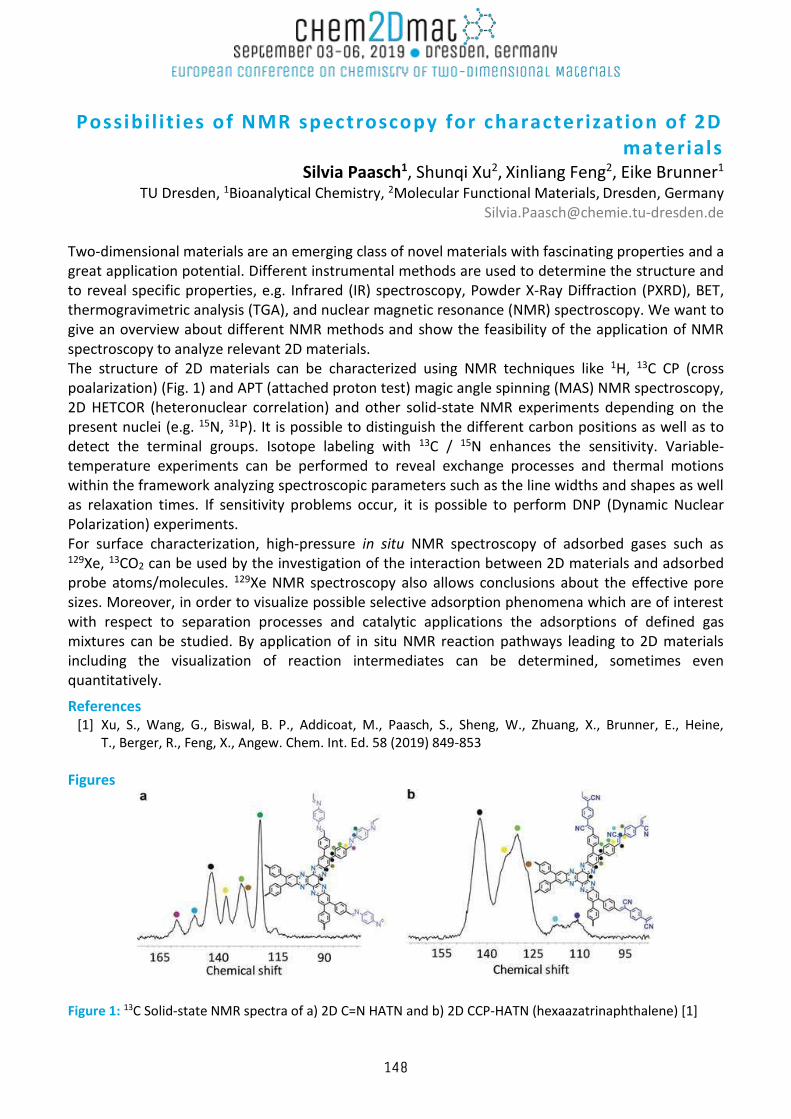
Possibi l i t ies of NMR spectroscopy for characterizat ion of 2D materials
Silvia Paasch1, Shunqi Xu2, Xinliang Feng2, Eike Brunner1 TU Dresden, 1Bioanalytical Chemistry, 2Molecular Functional Materials, Dresden, Germany
Two-dimensional materials are an emerging class of novel materials with fascinating properties and a great application potential. Different instrumental methods are used to determine the structure and to reveal specific properties, e.g. Infrared (IR) spectroscopy, Powder X-Ray Diffraction (PXRD), BET, thermogravimetric analysis (TGA), and nuclear magnetic resonance (NMR) spectroscopy. We want to give an overview about different NMR methods and show the feasibility of the application of NMR spectroscopy to analyze relevant 2D materials. The structure of 2D materials can be characterized using NMR techniques like 1H, 13C CP (cross poalarization) (Fig. 1) and APT (attached proton test) magic angle spinning (MAS) NMR spectroscopy, 2D HETCOR (heteronuclear correlation) and other solid-state NMR experiments depending on the present nuclei (e.g. 15N, 31P). It is possible to distinguish the different carbon positions as well as to detect the terminal groups. Isotope labeling with 13C / 15N enhances the sensitivity. Variable-temperature experiments can be performed to reveal exchange processes and thermal motions within the framework analyzing spectroscopic parameters such as the line widths and shapes as well as relaxation times. If sensitivity problems occur, it is possible to perform DNP (Dynamic Nuclear Polarization) experiments. For surface characterization, high-pressure in situ NMR spectroscopy of adsorbed gases such as 129Xe, 13CO2 can be used by the investigation of the interaction between 2D materials and adsorbed probe atoms/molecules. 129Xe NMR spectroscopy also allows conclusions about the effective pore sizes. Moreover, in order to visualize possible selective adsorption phenomena which are of interest with respect to separation processes and catalytic applications the adsorptions of defined gas mixtures can be studied. By application of in situ NMR reaction pathways leading to 2D materials including the visualization of reaction intermediates can be determined, sometimes even quantitatively.
References [1] Xu, S., Wang, G., Biswal, B. P., Addicoat, M., Paasch, S., Sheng, W., Zhuang, X., Brunner, E., Heine,
T., Berger, R., Feng, X., Angew. Chem. Int. Ed. 58 (2019) 849-853
Figures
Figure 1: 13C Solid-state NMR spectra of a) 2D C=N HATN and b) 2D CCP-HATN (hexaazatrinaphthalene) [1]
148
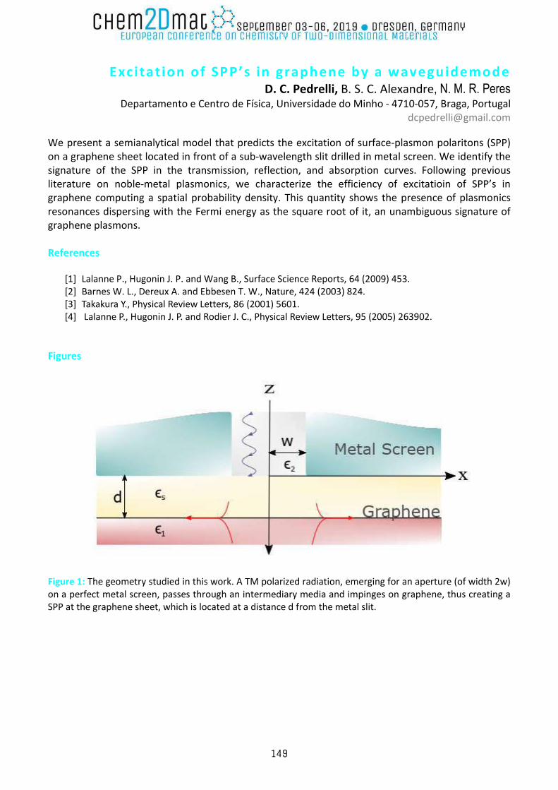
Excitat ion of SPP’s in graphene by a waveguidemodeD. C. Pedrelli, B. S. C. Alexandre, N. M. R. Peres
Departamento e Centro de Física, Universidade do Minho - 4710-057, Braga, [email protected]
We present a semianalytical model that predicts the excitation of surface-plasmon polaritons (SPP)on a graphene sheet located in front of a sub-wavelength slit drilled in metal screen. We identify thesignature of the SPP in the transmission, reflection, and absorption curves. Following previousliterature on noble-metal plasmonics, we characterize the efficiency of excitatioin of SPP’s ingraphene computing a spatial probability density. This quantity shows the presence of plasmonicsresonances dispersing with the Fermi energy as the square root of it, an unambiguous signature ofgraphene plasmons.
References
[1] Lalanne P., Hugonin J. P. and Wang B., Surface Science Reports, 64 (2009) 453.[2] Barnes W. L., Dereux A. and Ebbesen T. W., Nature, 424 (2003) 824.[3] Takakura Y., Physical Review Letters, 86 (2001) 5601.[4] Lalanne P., Hugonin J. P. and Rodier J. C., Physical Review Letters, 95 (2005) 263902.
Figures
Figure 1: The geometry studied in this work. A TM polarized radiation, emerging for an aperture (of width 2w)on a perfect metal screen, passes through an intermediary media and impinges on graphene, thus creating aSPP at the graphene sheet, which is located at a distance d from the metal slit.
149
Photoswitching of commercial azobenzenes in di fferent environments
V. Quintano,[1] A. Kovtun,[1] F. Liscio,[2] A. Liscio,[3] V. Palermo[1,4] [1] CNR-ISOF, via P. Gobetti 101, 40129 Bologna, Italy
[2] CNR-IMM sezione di Bologna, via P. Gobetti 101, 40129 Bologna, Italy [3] CNR-IMM sezione di Roma, via del Fosso del Cavaliere 100, 00133 Roma, Italy
[4] Chalmers University of Technology, Chalmersplatsen 4, 412 96 Göteborg, Svezia
Molecular switches are a class of molecules able, upon optical or thermal stimuli, to change their chemical structure in a reversible way. They have been extensively studied for useful applications in electronics and sensing[1] attracting more and more interest from scientific community, resulting in the nobel prise in Chemistry assigned in 2016 to Sauvage, Stoddart and Feringa.[2] One of the most well-known class of switching molecules is the one of azobenzenes[add general description of azobenzenes and citations] whose fundamental properties have been extensively studied and they are also currently used at industrial level, as example up to 70% of the world’s commercial dyes are based on azobenzene.[1] Often, their optical properties are studied in solution; though, in most of the possible industrial applications[3], from (opto)electronics to composite materials, azobenzenes are in solid environments; as example, applications in electronics require the azobenzenes to be deposited on a 2D substrate, possibly in ordered layers.[4] Applications as industrial dyes require the azobenzenes to be dispersed in a 3D material (typically a polymer). Here, we study the properties of two commercial azobenzene molecules, and how its cis-trans switching behavior is influenced when the molecule is solubilized in different solvents, dispersed in polymers, deposited on a substrate or arranged in 3D crystals. To study the molecule in so many different systems, we have to use a combination of different techniques to study the morphological and the electronic properties, such as Scanning Probe Microscopies, conventional and time-resolved UV-vis spectroscopies and X-ray Photoelectron Spectroscopies.
References [1] Leigh, D.A., Genesis of the Nanomachines: The 2016 Nobel Prize in Chemistry. Angewandte Chemie-International Edition, 2016. 55(47): p. 14506-14508. [2] Armaroli, N. and V. Balzani, The future of energy supply: Challenges and opportunities. Angewandte Chemie-International Edition, 2007. 46(1-2): p. 52-66. [3] Zollinger, H., Color chemistry : syntheses, properties, and applications of organic dyes and pigments. 3rd, rev. ed. 2003, Zurich Weinheim: Verlag Helvetica Chimica Acta; Wiley-VCH. x, 637 p. [4] Crivillers, N., et al., Photoinduced work function changes by isomerization of a densely packed azobenzene-based SAM on Au: a joint experimental and theoretical study. Physical Chemistry Chemical Physics, 2011. 13(32): p. 14302-14310.
150
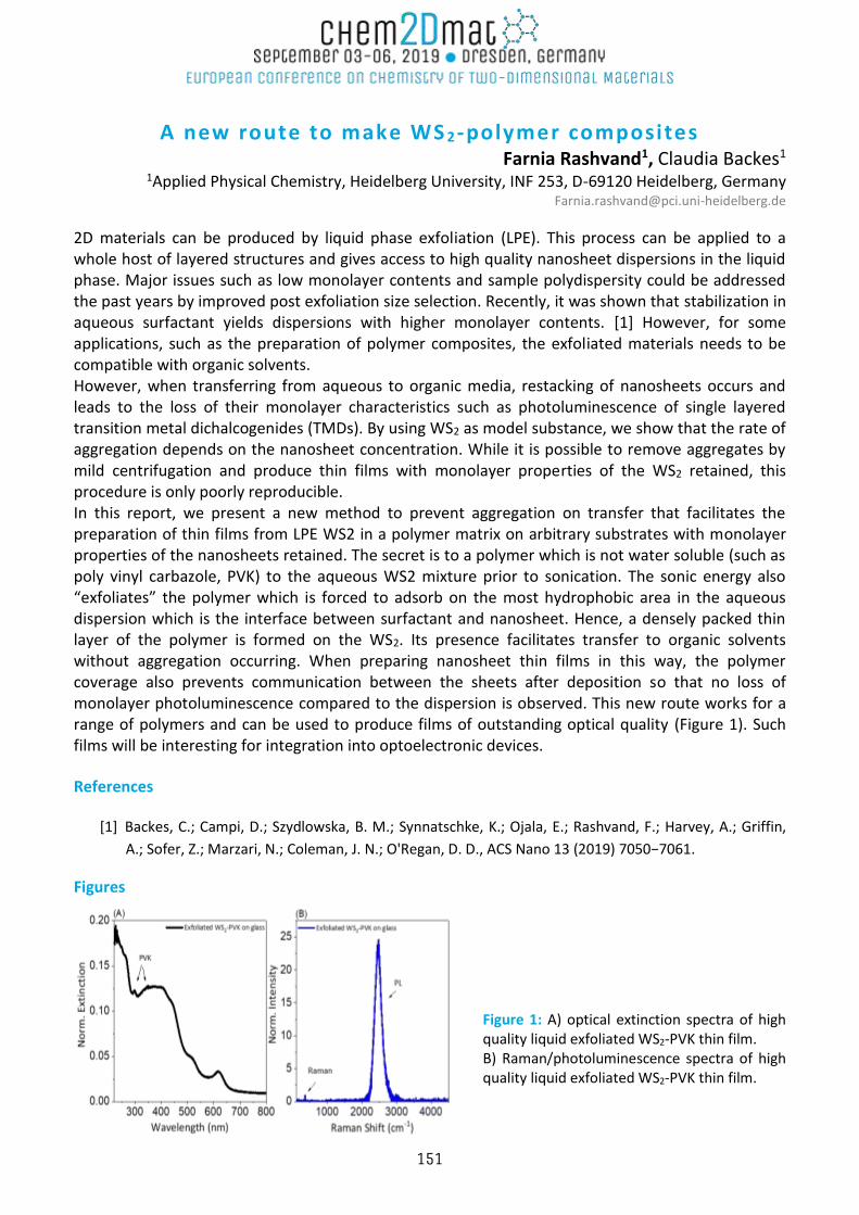
A new route to make WS 2 -polymer composites Farnia Rashvand1, Claudia Backes1
1Applied Physical Chemistry, Heidelberg University, INF 253, D-69120 Heidelberg, Germany [email protected]
2D materials can be produced by liquid phase exfoliation (LPE). This process can be applied to a whole host of layered structures and gives access to high quality nanosheet dispersions in the liquid phase. Major issues such as low monolayer contents and sample polydispersity could be addressed the past years by improved post exfoliation size selection. Recently, it was shown that stabilization in aqueous surfactant yields dispersions with higher monolayer contents. [1] However, for some applications, such as the preparation of polymer composites, the exfoliated materials needs to be compatible with organic solvents. However, when transferring from aqueous to organic media, restacking of nanosheets occurs and leads to the loss of their monolayer characteristics such as photoluminescence of single layered transition metal dichalcogenides (TMDs). By using WS2 as model substance, we show that the rate of aggregation depends on the nanosheet concentration. While it is possible to remove aggregates by mild centrifugation and produce thin films with monolayer properties of the WS2 retained, this procedure is only poorly reproducible. In this report, we present a new method to prevent aggregation on transfer that facilitates the preparation of thin films from LPE WS2 in a polymer matrix on arbitrary substrates with monolayer properties of the nanosheets retained. The secret is to a polymer which is not water soluble (such as poly vinyl carbazole, PVK) to the aqueous WS2 mixture prior to sonication. The sonic energy also “exfoliates” the polymer which is forced to adsorb on the most hydrophobic area in the aqueous dispersion which is the interface between surfactant and nanosheet. Hence, a densely packed thin layer of the polymer is formed on the WS2. Its presence facilitates transfer to organic solvents without aggregation occurring. When preparing nanosheet thin films in this way, the polymer coverage also prevents communication between the sheets after deposition so that no loss of monolayer photoluminescence compared to the dispersion is observed. This new route works for a range of polymers and can be used to produce films of outstanding optical quality (Figure 1). Such films will be interesting for integration into optoelectronic devices.
References
[1] Backes, C.; Campi, D.; Szydlowska, B. M.; Synnatschke, K.; Ojala, E.; Rashvand, F.; Harvey, A.; Griffin,
A.; Sofer, Z.; Marzari, N.; Coleman, J. N.; O'Regan, D. D., ACS Nano 13 (2019) 7050−7061.
Figures
Figure 1: A) optical extinction spectra of high quality liquid exfoliated WS2-PVK thin film. B) Raman/photoluminescence spectra of high quality liquid exfoliated WS2-PVK thin film.
151
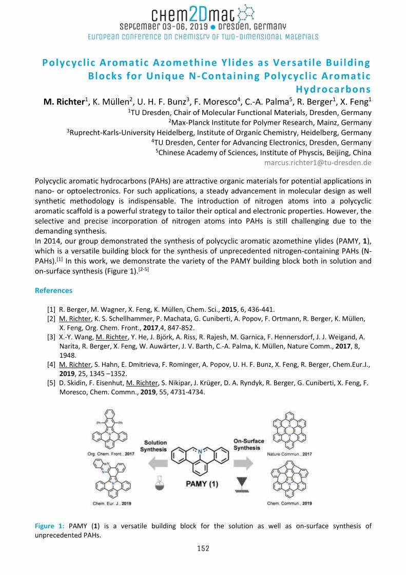
Polycycl ic Aromatic Azomethine Yl ides as Versati le Building Blocks for Unique N-Containing Polycycl ic Aromatic
Hydrocarbons M. Richter1, K. Müllen2, U. H. F. Bunz3, F. Moresco4, C.-A. Palma5, R. Berger1, X. Feng1
1TU Dresden, Chair of Molecular Functional Materials, Dresden, Germany 2Max-Planck Institute for Polymer Research, Mainz, Germany
3Ruprecht-Karls-University Heidelberg, Institute of Organic Chemistry, Heidelberg, Germany 4TU Dresden, Center for Advancing Electronics, Dresden, Germany
5Chinese Academy of Sciences, Institute of Physcis, Beijing, China [email protected]
Polycyclic aromatic hydrocarbons (PAHs) are attractive organic materials for potential applications in nano- or optoelectronics. For such applications, a steady advancement in molecular design as well synthetic methodology is indispensable. The introduction of nitrogen atoms into a polycyclic aromatic scaffold is a powerful strategy to tailor their optical and electronic properties. However, the selective and precise incorporation of nitrogen atoms into PAHs is still challenging due to the demanding synthesis. In 2014, our group demonstrated the synthesis of polycyclic aromatic azomethine ylides (PAMY, 1), which is a versatile building block for the synthesis of unprecedented nitrogen-containing PAHs (N-PAHs).[1] In this work, we demonstrate the variety of the PAMY building block both in solution and on-surface synthesis (Figure 1).[2-5]
References
[1] R. Berger, M. Wagner, X. Feng, K. Müllen, Chem. Sci., 2015, 6, 436-441. [2] M. Richter, K. S. Schellhammer, P. Machata, G. Cuniberti, A. Popov, F. Ortmann, R. Berger, K. Müllen,
X. Feng, Org. Chem. Front., 2017,4, 847-852. [3] X.-Y. Wang, M. Richter, Y. He, J. Björk, A. Riss, R. Rajesh, M. Garnica, F. Hennersdorf, J. J. Weigand, A.
Narita, R. Berger, X. Feng, W. Auwärter, J. V. Barth, C.-A. Palma, K. Müllen, Nature Comm., 2017, 8, 1948.
[4] M. Richter, S. Hahn, E. Dmitrieva, F. Rominger, A. Popov, U. H. F. Bunz, X. Feng, R. Berger, Chem.Eur.J., 2019, 25, 1345 –1352.
[5] D. Skidin, F. Eisenhut, M. Richter, S. Nikipar, J. Krüger, D. A. Ryndyk, R. Berger, G. Cuniberti, X. Feng, F. Moresco, Chem. Commn., 2019, 55, 4731-4734.
Figure 1: PAMY (1) is a versatile building block for the solution as well as on-surface synthesis of unprecedented PAHs.
152
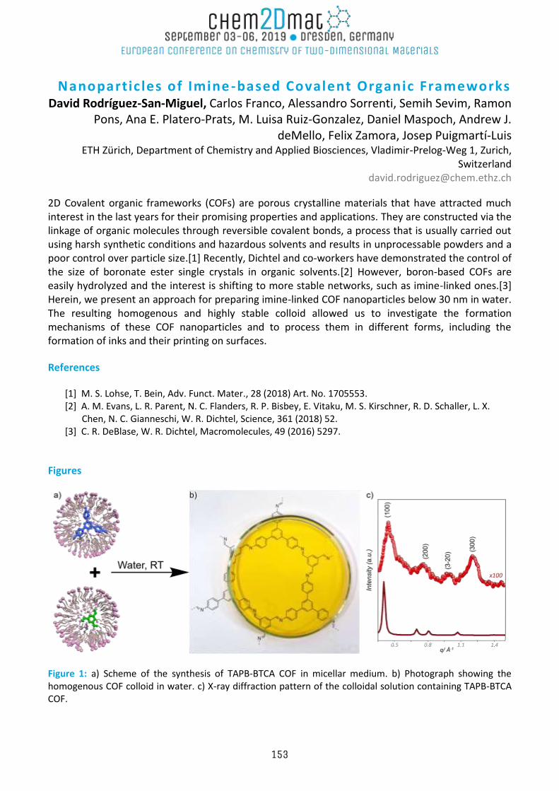
Nanopartic les of Imine -based Covalent Organic Frameworks David Rodríguez-San-Miguel, Carlos Franco, Alessandro Sorrenti, Semih Sevim, Ramon
Pons, Ana E. Platero-Prats, M. Luisa Ruiz-Gonzalez, Daniel Maspoch, Andrew J. deMello, Felix Zamora, Josep Puigmartí-Luis
ETH Zürich, Department of Chemistry and Applied Biosciences, Vladimir-Prelog-Weg 1, Zurich, Switzerland
2D Covalent organic frameworks (COFs) are porous crystalline materials that have attracted much interest in the last years for their promising properties and applications. They are constructed via the linkage of organic molecules through reversible covalent bonds, a process that is usually carried out using harsh synthetic conditions and hazardous solvents and results in unprocessable powders and a poor control over particle size.[1] Recently, Dichtel and co-workers have demonstrated the control of the size of boronate ester single crystals in organic solvents.[2] However, boron-based COFs are easily hydrolyzed and the interest is shifting to more stable networks, such as imine-linked ones.[3] Herein, we present an approach for preparing imine-linked COF nanoparticles below 30 nm in water. The resulting homogenous and highly stable colloid allowed us to investigate the formation mechanisms of these COF nanoparticles and to process them in different forms, including the formation of inks and their printing on surfaces.
References
[1] M. S. Lohse, T. Bein, Adv. Funct. Mater., 28 (2018) Art. No. 1705553. [2] A. M. Evans, L. R. Parent, N. C. Flanders, R. P. Bisbey, E. Vitaku, M. S. Kirschner, R. D. Schaller, L. X.
Chen, N. C. Gianneschi, W. R. Dichtel, Science, 361 (2018) 52. [3] C. R. DeBlase, W. R. Dichtel, Macromolecules, 49 (2016) 5297.
Figures
Figure 1: a) Scheme of the synthesis of TAPB-BTCA COF in micellar medium. b) Photograph showing the homogenous COF colloid in water. c) X-ray diffraction pattern of the colloidal solution containing TAPB-BTCA COF.
153
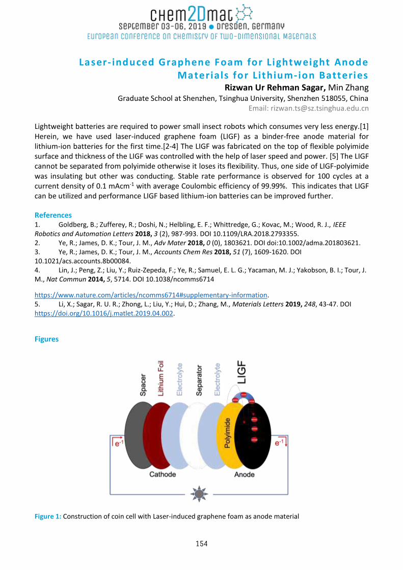
Laser- induced Graphene Foam for Lightweight Anode Materials for Lithium-ion Batteries
Rizwan Ur Rehman Sagar, Min Zhang Graduate School at Shenzhen, Tsinghua University, Shenzhen 518055, China
Email: [email protected]
Lightweight batteries are required to power small insect robots which consumes very less energy.[1] Herein, we have used laser-induced graphene foam (LIGF) as a binder-free anode material for lithium-ion batteries for the first time.[2-4] The LIGF was fabricated on the top of flexible polyimide surface and thickness of the LIGF was controlled with the help of laser speed and power. [5] The LIGF cannot be separated from polyimide otherwise it loses its flexibility. Thus, one side of LIGF-polyimide was insulating but other was conducting. Stable rate performance is observed for 100 cycles at a current density of 0.1 mAcm-1 with average Coulombic efficiency of 99.99%. This indicates that LIGF can be utilized and performance LIGF based lithium-ion batteries can be improved further. References 1. Goldberg, B.; Zufferey, R.; Doshi, N.; Helbling, E. F.; Whittredge, G.; Kovac, M.; Wood, R. J., IEEE Robotics and Automation Letters 2018, 3 (2), 987-993. DOI 10.1109/LRA.2018.2793355. 2. Ye, R.; James, D. K.; Tour, J. M., Adv Mater 2018, 0 (0), 1803621. DOI doi:10.1002/adma.201803621. 3. Ye, R.; James, D. K.; Tour, J. M., Accounts Chem Res 2018, 51 (7), 1609-1620. DOI 10.1021/acs.accounts.8b00084. 4. Lin, J.; Peng, Z.; Liu, Y.; Ruiz-Zepeda, F.; Ye, R.; Samuel, E. L. G.; Yacaman, M. J.; Yakobson, B. I.; Tour, J. M., Nat Commun 2014, 5, 5714. DOI 10.1038/ncomms6714
https://www.nature.com/articles/ncomms6714#supplementary-information. 5. Li, X.; Sagar, R. U. R.; Zhong, L.; Liu, Y.; Hui, D.; Zhang, M., Materials Letters 2019, 248, 43-47. DOI https://doi.org/10.1016/j.matlet.2019.04.002.
Figures
Figure 1: Construction of coin cell with Laser-induced graphene foam as anode material
154
Graphene Dispersions Prepared with Pyrene Derivatives and use in Cel l Internalisation and s iRNA Complexation Assays
Yuyoung Shin1, Xavier Just-Baringo1, Sandra Vranic2, Sai Manoj Gali3,
Alexandra Gkoutzidou4, Eric Prestat4,6, David Beljonne3, Igor Larrosa1, Kostas Kostarelos2, Cinzia Casiraghi1
1School of Chemistry, University of Manchester, Oxford Road, Manchester, UK 2Nanomedicine Lab, AV Hill Building, University of Manchester, Manchester, UK
3Laboratory for Chemistry of Novel Materials, University of Mons, Mons, Belgium 4School of Materials, University of Manchester, Oxford Road, Manchester, UK
5Dalton Cumbrian Facility, University of Manchester, Westlakes Science and Technology Park, Moor Row, Cumbria, UK
6SuperSTEM Laboratory, SciTech Daresbury Campus, Daresbury, UK Contact@ [email protected]
Liquid-phase exfoliation (LPE) is a simple, mass-scalable and cost effective method to produce solution processed graphene [1,2]. To effectively disperse defects-free graphene in water, which is needed in biological applications, a stabilizer must be used [3]. Anionic pyrene derivatives have been shown to be very effective at exfoliating graphite, compared to traditional surfactants [4-6]. However, only very few studies have reported the use of cationic pyrene derivatives, giving rise to low concentration and/or limited dispersion stability [7.8]. Amphoteric pyrene-derivatives were also reported, however with limited stability at neutral pH [9]. In this work we produced and tested various cationic pyrene derivatives as stabilizers in LPE in water. By designing pyrene derivatives with different functional groups and variable distance between pyrene and the charged group, we have been able to get insights on the exfoliation mechanism and to understand how to design the pyrene derivative to achieve efficient exfoliation [10]. The graphene dispersions produced with such pyrene derivatives show excellent biocompatibility, cell internalization capacity, and colloidal stability even in the biological environment [10]. By taking advantage of the positive charge of such graphene flakes, we have tested the material for siRNA complexation, obtaining better siRNA complex formation than with negatively charged graphene, including graphene oxide [10,11]. In conclusion, in this work we demonstrate that highly concentrated, stable and biocompatible graphene dispersions with positive charge can be easily produced by LPE in water by using designed cationic pyrene derivatives. This material shows great potential for biological applications.
References [1] Novoselov, K., et al. Nature, 490, (2012), 192. [2] Hernandez, Y., et al. Nature Nanotechnology, 3, (2008), 563. [3] Lotya, M., et al. JACS, 131, (2009), 3611. [4] Yang, H.,et al., Carbon, 53, (2013), 357-365. [5] Parviz, D., et al., ACS Nano, 6(10), (2012) 8857-8867. [6] Schlierf, A., et al. Nanoscale, 5.10 (2013): 4205-4216. [7] Li, W., et al., Physical Chemistry Chemical Physics, 19(26), (2017), 17036-17043. [8] Malig, J.,et al., Advanced Materials, 24(6), (2012), 800-805. [9] Shin, Y. et al. Molecular Systems Design & Engineering (2019). DOI:10.1039/C9ME00024K [10] Shin, Y. et al, submitted [11] de Lazaro, I., et al. bioRxiv (2018): 486522.
155
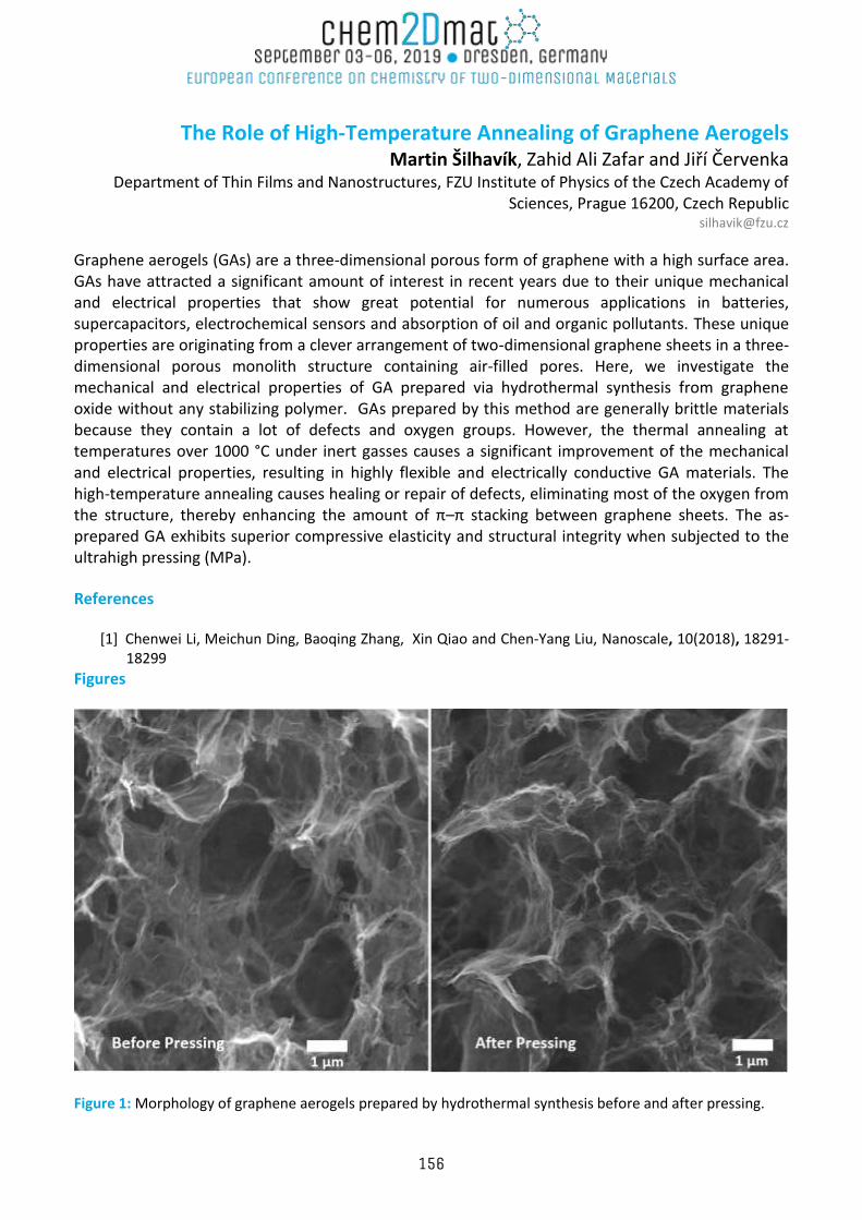
The Role of High-Temperature Annealing of Graphene Aerogels Martin Šilhavík, Zahid Ali Zafar and Jiří Červenka
Department of Thin Films and Nanostructures, FZU Institute of Physics of the Czech Academy of Sciences, Prague 16200, Czech Republic
Graphene aerogels (GAs) are a three-dimensional porous form of graphene with a high surface area. GAs have attracted a significant amount of interest in recent years due to their unique mechanical and electrical properties that show great potential for numerous applications in batteries, supercapacitors, electrochemical sensors and absorption of oil and organic pollutants. These unique properties are originating from a clever arrangement of two-dimensional graphene sheets in a three-dimensional porous monolith structure containing air-filled pores. Here, we investigate the mechanical and electrical properties of GA prepared via hydrothermal synthesis from graphene oxide without any stabilizing polymer. GAs prepared by this method are generally brittle materials because they contain a lot of defects and oxygen groups. However, the thermal annealing at temperatures over 1000 °C under inert gasses causes a significant improvement of the mechanical and electrical properties, resulting in highly flexible and electrically conductive GA materials. The high-temperature annealing causes healing or repair of defects, eliminating most of the oxygen from the structure, thereby enhancing the amount of π–π stacking between graphene sheets. The as-prepared GA exhibits superior compressive elasticity and structural integrity when subjected to the ultrahigh pressing (MPa).
References
[1] Chenwei Li, Meichun Ding, Baoqing Zhang, Xin Qiao and Chen-Yang Liu, Nanoscale, 10(2018), 18291-18299
Figures
Figure 1: Morphology of graphene aerogels prepared by hydrothermal synthesis before and after pressing.
156
Inorganic-organic Heterostructures formed by Non-Covalent Functionalization of MoS 2
Rita Siris, Tanja Stimpel-Lindner, Siwei Luo***, Connor Cullen**, Corinna Weiß*, Frank Hauke*, Georg S. Duesberg
Institute of Physics, EIT 2, Faculty of Electrical Engineering and Information Technology, Universität der Bundeswehr München, Germany
*Institute of Advanced Materials and Processes, ZMP, Group of Functional Carbon Allotropes, University Erlangen-Nuernberg, Germany
**Centre for Research on Adaptive Nanostructures and Nanodevices (CRANN), Trinity College Dublin, Ireland
***Hunan Key Laboratory for Micro-Nano Energy Materials and Devices, Laboratory for Quantum Engineering and Micro-Nano Energy Technology, and School of Physics and Optoelectronics, Xiangtan
University, Hunan, People’s Republic of China [email protected]
Abstract Transition metal dichalcogenides (TMDs) represent a class of layered 2D materials with exciting electronic, optical and mechanical properties, making them suitable candidates for diverse applications in the fields of electronics and optoelectronics. Due to their layered, high surface nature the properties of 2D materials strongly depend on the environment, offering highly variable platforms for on-surface chemical modification and functionalization. Therefore, merging the fields of non-covalent organic functionalization and 2D TMDs can lead to doping via charge transfer, resulting in tunable electrical properties in the heterostructures, which can be exploited in electrical devices such as diodes, FETs, chemiresistors or ChemFETs. The approach discussed in this contribution includes non-covalent functionalization of organic molecules onto monolayer CVD grown MoS2, forming self-assembled monolayers (SAMs) through van der Waals interactions. In particular, we focus on the on-chip non-covalent functionalization with perylene bisimide molecules, forming surface functionalized MoS2 or molecule-encapsulated structures. The effect of molecular functionalization is investigated with Raman spectroscopy, XPS, TOF-SIMS surface analysis and scanning probe techniques. The potential of hybrid inorganic-organic structures is pointed out within this study, giving rise to possible electronic and optoelectronic applications.
References
[1] N. C. Berner, S. Winters, C. Backes, C. Yim, K. C. Dümbgen, I. Kaminska, S. Mackowski, A. A. Cafolla, A. Hirsch, G. S. Duesberg, Nanoscale, 7 (2015), 16337.
[2] S. Winters, S. Winters, N. C. Berner, R. Mishra, K. C. Dümbgen, C. Backes, M. Hegner, A. Hirsch, G. S. Duesberg, Chem. Commun., 51 (2015),16778.
[3] H. Kim, W. Kim, M. O’Brien, N. McEvoy, C. Yim, M. Marcia, F. Hauke, A. Hirsch, G. Kim, G. S. Duesberg, Nanoscale,10 (2018), 17557.
157
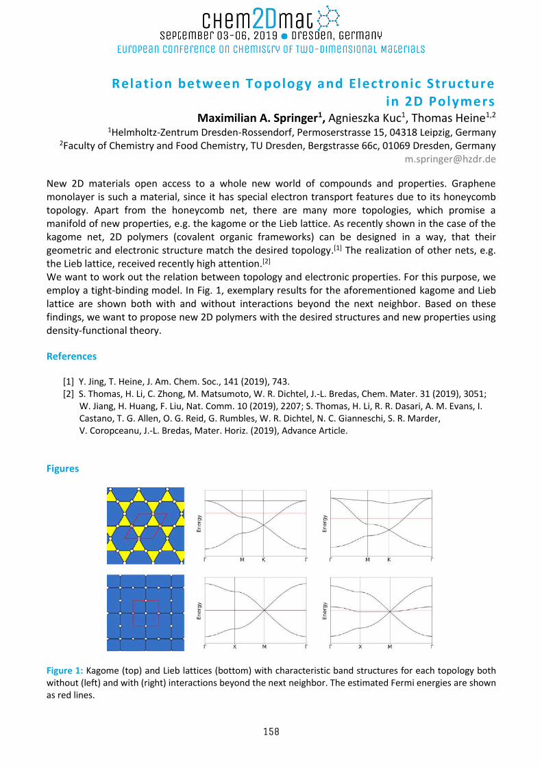
Relation between To pology and Electronic Structure in 2D Polymers
Maximilian A. Springer1, Agnieszka Kuc1, Thomas Heine1,2
1Helmholtz-Zentrum Dresden-Rossendorf, Permoserstrasse 15, 04318 Leipzig, Germany 2Faculty of Chemistry and Food Chemistry, TU Dresden, Bergstrasse 66c, 01069 Dresden, Germany
[email protected] New 2D materials open access to a whole new world of compounds and properties. Graphene monolayer is such a material, since it has special electron transport features due to its honeycomb topology. Apart from the honeycomb net, there are many more topologies, which promise a manifold of new properties, e.g. the kagome or the Lieb lattice. As recently shown in the case of the kagome net, 2D polymers (covalent organic frameworks) can be designed in a way, that their geometric and electronic structure match the desired topology.[1] The realization of other nets, e.g. the Lieb lattice, received recently high attention.[2] We want to work out the relation between topology and electronic properties. For this purpose, we employ a tight-binding model. In Fig. 1, exemplary results for the aforementioned kagome and Lieb lattice are shown both with and without interactions beyond the next neighbor. Based on these findings, we want to propose new 2D polymers with the desired structures and new properties using density-functional theory.
References
[1] Y. Jing, T. Heine, J. Am. Chem. Soc., 141 (2019), 743. [2] S. Thomas, H. Li, C. Zhong, M. Matsumoto, W. R. Dichtel, J.-L. Bredas, Chem. Mater. 31 (2019), 3051;
W. Jiang, H. Huang, F. Liu, Nat. Comm. 10 (2019), 2207; S. Thomas, H. Li, R. R. Dasari, A. M. Evans, I. Castano, T. G. Allen, O. G. Reid, G. Rumbles, W. R. Dichtel, N. C. Gianneschi, S. R. Marder, V. Coropceanu, J.-L. Bredas, Mater. Horiz. (2019), Advance Article.
Figures
Figure 1: Kagome (top) and Lieb lattices (bottom) with characteristic band structures for each topology both without (left) and with (right) interactions beyond the next neighbor. The estimated Fermi energies are shown as red lines.
158
Covalent modification of graphite via iodonium salts: A versati le alternative to diazonium salts.
Roelof Steeno, Kunal S. Mali, Steven De Feyter KU Leuven, Department of Chemistry, Division of Molecular Imaging and Photonics, Leuven,
Belgium-3001 [email protected]
Covalent modification of carbon materials with organic functional groups is highly desired as it allows manipulation of their functional properties. Diazonium chemistry has remained a method of choice since it was first applied in 1992 for covalent attachment of aryl groups onto the surface of an amorphous carbon electrode.[1] Reductive decomposition of diazonium salts, which can be achieved electrochemically, chemically, or photochemically, to produce aryl radicals has been used for modification of a wide variety of substrates including graphene and MoS2.[2,3]
While diazonium salts have proven to be versatile over the years, they are often unstable under ambient conditions necessitating their generation in-situ during the functionalization protocol. This complicates the already complex process of surface functionalization. Secondly, their high reactivity, while desired for modification of unreactive substrates such as graphene, often leads to side reactions that are difficult to control.
In this contribution, I will discuss the use of iodonium salts for covalent functionalization of graphite and graphene. Iodonium salts are known to be stable under ambient conditions compared to their diazonium counterparts and hence provide a comparatively simpler alternative. Furthermore, in contrast to aryl diazonium salts, this chemistry allows attachment of heterocycles[4], and alkynyl groups[5] groups to the surface. The covalent modification of graphite and graphene using electrochemical decomposition of iodonium salts will be discussed. The in-depth characterization of the modified surface using atomic force microscopy (AFM), scanning tunneling microscopy (STM) and Raman spectroscopy will be presented. Finally, a thorough comparison between the surfaces modified using diazonium chemistry and iodonium chemistry will be presented.
References [1] JM. Savéant, J. Pinson, R. Hitmi and M Delamar, JACS 1992, 114, 5883-5884. [2] F. I. Podvorica, J. Pinson, M. M. Chehimi and A. Berisha, Electroanalytical Chemistry: A Series of Advances
2016, 26, 115-223 [3] C. Backes, J. N. Coleman, A. Hirsch, F. Hauke, V. Nicolosi, G. S. Duesberg, S. Sanvito, M. Halik, P. Vecera, I.
Abramovic, Z. Wang, N. McEvoy, Z. Gholamvand, C. S. Cucinotta, H. C. Nerl, N. C. Berner and K. C. Knirsch , ACS Nano 2015, 9, 6018-6030
[4] K. Daasbjerg, S. U. Pedersen and A. Sommerfeldt, Electrochimica Acta 2018, 261, 356-364
[5] C. Coutanceau, S. Baranton and M. Weissmann, Langmuir 2010, 26, 15002-15009
159
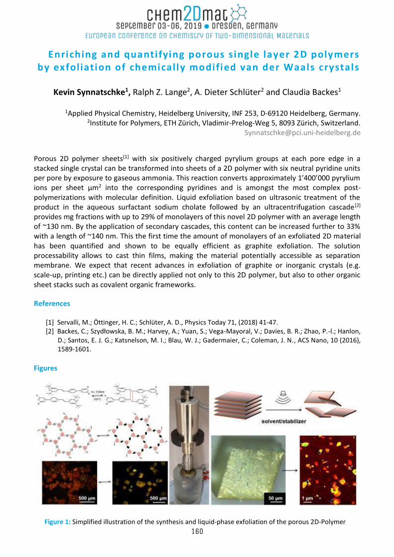
Enriching and quanti fying porous single layer 2D polymers by exfol iation of chemical ly modified van der Waals crystals
Kevin Synnatschke1, Ralph Z. Lange2, A. Dieter Schlüter2 and Claudia Backes1
1Applied Physical Chemistry, Heidelberg University, INF 253, D-69120 Heidelberg, Germany.
2Institute for Polymers, ETH Zürich, Vladimir-Prelog-Weg 5, 8093 Zürich, Switzerland. [email protected]
Porous 2D polymer sheets[1] with six positively charged pyrylium groups at each pore edge in a stacked single crystal can be transformed into sheets of a 2D polymer with six neutral pyridine units per pore by exposure to gaseous ammonia. This reaction converts approximately 1’400’000 pyrylium ions per sheet µm2 into the corresponding pyridines and is amongst the most complex post-polymerizations with molecular definition. Liquid exfoliation based on ultrasonic treatment of the product in the aqueous surfactant sodium cholate followed by an ultracentrifugation cascade[2] provides mg fractions with up to 29% of monolayers of this novel 2D polymer with an average length of ~130 nm. By the application of secondary cascades, this content can be increased further to 33% with a length of ~140 nm. This the first time the amount of monolayers of an exfoliated 2D material has been quantified and shown to be equally efficient as graphite exfoliation. The solution processability allows to cast thin films, making the material potentially accessible as separation membrane. We expect that recent advances in exfoliation of graphite or inorganic crystals (e.g. scale-up, printing etc.) can be directly applied not only to this 2D polymer, but also to other organic sheet stacks such as covalent organic frameworks. References
[1] Servalli, M.; Öttinger, H. C.; Schlüter, A. D., Physics Today 71, (2018) 41-47. [2] Backes, C.; Szydłowska, B. M.; Harvey, A.; Yuan, S.; Vega-Mayoral, V.; Davies, B. R.; Zhao, P.-l.; Hanlon,
D.; Santos, E. J. G.; Katsnelson, M. I.; Blau, W. J.; Gadermaier, C.; Coleman, J. N., ACS Nano, 10 (2016), 1589-1601.
Figures
Figure 1: Simplified illustration of the synthesis and liquid-phase exfoliation of the porous 2D-Polymer 160
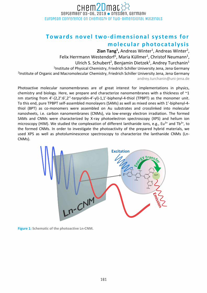
To wards no ve l tw o -d imen siona l sys tems fo r
mo lecu lar pho to cata lys i s Zian Tang1, Andreas Winter1, Andreas Winter2,
Felix Herrmann Westendorf1, Maria Küllmer1, Christof Neumann1, Ulrich S. Schubert2, Benjamin Dietzek1, Andrey Turchanin1
1Institute of Physical Chemistry, Friedrich Schiller University Jena, Jena Germany 2Institute of Organic and Macromolecular Chemistry, Friedrich Schiller University Jena, Jena Germany
Photoactive molecular nanomembranes are of great interest for implementations in physics, chemistry and biology. Here, we prepare and characterize nanomembranes with a thickness of ~1 nm starting from 4’-(2,2’:6’,2’’-terpyridin-4’-yl)-1,1’-biphenyl-4-thiol (TPBPT) as the monomer unit. To this end, pure TPBPT self-assembled monolayers (SAMs) as well as mixed ones with 1’-biphenyl-4-thiol (BPT) as co-monomers were assembled on Au substrates and crosslinked into molecular nanosheets, i.e. carbon nanomembranes (CNMs), via low-energy electron irradiation. The formed SAMs and CNMs were characterized by X-ray photoelectron spectroscopy (XPS) and helium ion microscopy (HIM). We studied the complexation of different lanthanide ions, e.g., Eu3+ and Tb3+, to the formed CNMs. In order to investigate the photoactivity of the prepared hybrid materials, we used XPS as well as photoluminescence spectroscopy to characterize the lanthanide CNMs (Ln-CNMs).
Figure 1: Schematic of the photoactive Ln-CNM.
161
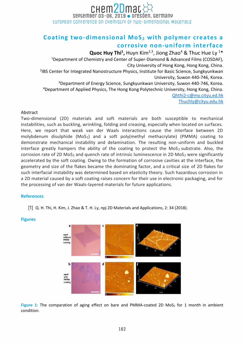
Coating two-dimensional MoS 2 with polymer creates a corrosive non-uniform interface
Quoc Huy Thi1, Huyn Kim2,3, Jiong Zhao4 & Thuc Hue Ly 1* 1Department of Chemistry and Center of Super-Diamond & Advanced Films (COSDAF),
City University of Hong Kong, Hong Kong, China. 2IBS Center for Integrated Nanostructure Physics, Institute for Basic Science, Sungkyunkwan
University, Suwon 440-746, Korea. 3Department of Energy Science, Sungkyunkwan University, Suwon 440-746, Korea.
4Department of Applied Physics, The Hong Kong Polytechnic University, Hong Kong, China. [email protected]
Abstract Two-dimensional (2D) materials and soft materials are both susceptible to mechanical instabilities, such as buckling, wrinkling, folding and creasing, especially when located on surfaces. Here, we report that weak van der Waals interactions cause the interface between 2D molybdenum disulphide (MoS2) and a soft poly(methyl methacrylate) (PMMA) coating to demonstrate mechanical instability and delamination. The resulting non-uniform and buckled interface greatly hampers the ability of the coating to protect the MoS2 substrate. Also, the corrosion rate of 2D MoS2 and quench rate of intrinsic luminescence in 2D MoS2 were significantly accelerated by the soft coating. Owing to the formation of corrosive cavities at the interface, the geometry and size of the flakes became the dominating factor, and a critical size of 2D flakes for such interfacial instability was determined based on elasticity theory. Such hazardous corrosion in a 2D material caused by a soft coating raises concern for their use in electronic packaging, and for the processing of van der Waals-layered materials for future applications.
References
[1] Q. H. Thi, H. Kim, J. Zhao & T. H. Ly, npj 2D Materials and Applications, 2: 34 (2018).
Figures
Figure 1: The comparation of aging effect on bare and PMMA-coated 2D MoS2 for 1 month in ambient condition.
162
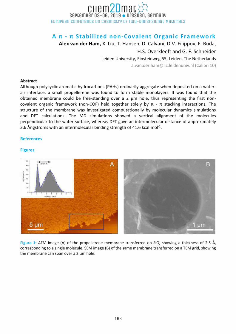
A π - π Stabil ized non-Covalent Organic Framework Alex van der Ham, X. Liu, T. Hansen, D. Calvani, D.V. Filippov, F. Buda,
H.S. Overkleeft and G. F. Schneider Leiden University, Einsteinweg 55, Leiden, The Netherlands
[email protected] (Calibri 10)
Abstract Although polycyclic aromatic hydrocarbons (PAHs) ordinarily aggregate when deposited on a water-air interface, a small propellerene was found to form stable monolayers. It was found that the obtained membrane could be free-standing over a 2 μm hole, thus representing the first non-covalent organic framework (non-COF) held together solely by π - π stacking interactions. The structure of the membrane was investigated computationally by molecular dynamics simulations and DFT calculations. The MD simulations showed a vertical alignment of the molecules perpendicular to the water surface, whereas DFT gave an intermolecular distance of approximately 3.6 Ångstroms with an intermolecular binding strength of 41.6 kcal·mol-1.
References
Figures
Figure 1: AFM image (A) of the propellerene membrane transferred on SiO, showing a thickness of 2.5 Å, corresponding to a single molecule. SEM image (B) of the same membrane transferred on a TEM grid, showing the membrane can span over a 2 μm hole.
163
Graphene l iquid cel ls for visual ization of wet samples by transmission electron microscopy at ambient temperature
Pauline M.G. van Deursen, P. Papadopoulou, Niek S.A. Crone, Roman I. Koning, Abraham J. Koster, Alexander Kros, Grégory F. Schneider
Leiden University, Netherlands [email protected]
Cryo-electron microscopy enables visualization of vitrified biological molecules and molecular assemblies, but does not allow the study of water-based processes as they occur, for example, in living organisms. Fixation of liquid-based specimen between graphene allows the visualization room-temperature samples and processes in the TEM. Our group developed a high-yield method for graphene liquid cell formation on a TEM grid, enabling us to encapsulate gold nanoparticles in water as well as whole bacterial cells. The protective properties of graphene against beam damage are such that graphene-fixated sample withstand extended periods of beam exposure, allowing 3D tomography reconstructions based on an unprecedented number of slices. The most exciting promise of graphene liquid phase electron microscopy, meanwhile, lies in the atomic resolution imaging of liquid-based processes. The methods presented in this work – particularly the reproducibility and simplicity of fabrication – enable the high resolution imaging of dynamic biomolecular systems.
164
Electrochemical sensing of phenols on f lat carbon surfaces functionalized with di fferent chemical groups
Fabio Vulcano1,2, Chiara Zanardi1,2, Andrea Liscio3, Andrea Candini2, Alessandro
Kovtun2, Emanuele Treossi2, Vincenzo Palermo2,4
1Department of Chemical and Geological Sciences, Università di Modena e Reggio Emilia, Via G. Campi 103, 41125 Modena, Italy
2Institute of Organic Synthesis and Photoreactivity (ISOF), National Research Council of Italy (CNR), via P. Gobetti 101 - 40129 Bologna, Italy
3Istitute of Microelectronics and Microsystems (IMM), National Research Council of Italy (CNR), via del Fosso del Cavaliere 100 - 00133 Rome, Italy
4Department of Industrial and Materials Science, Chalmers University of Technology, SE-412 96 Gothenburg, Sweden
E-mail: [email protected]
Graphene oxide is an interesting material for (bio)sensing[1], thanks to its tunable electrical conductivity and surface. It is very easy to tune its surface chemistry by varying the amount of epoxy, hydroxy and carboxy groups. Though, this rich surface chemistry makes also very difficult to understand the role of each functional group[2]. In this work, we tried to tackle this problem by creating thin layers of GO on otherwise perfect substrates of highly oriented pyrolitic graphite (HOPG). We compared the properties of pristine HOPG with activated HOPG (namely HOPGact), prepared following an electrochemical procedure previously described[3], that consist in an oxidation in an acidic medium that leads to the formation of hydroxyl, carbonilic and carboxyl groups, for the oxidative sensing of phenol derivatives. Phenols are an important class of organic compounds that can be found in different environments: they occur in foodstuff and plants (i.e. polyphenols) but also in drugs of abuse (e.g. morphine and cannabinoids). We first characterized HOPG and HOPGact surfaces by atomic force microscopy (AFM), X-rays photoemission spectroscopy (XPS) and cyclic voltammetry (CV) measurements using a common redox probe, namely 1,1’-ferrocenedimethanol. We then compared the performance of HOPG and HOPGact in CV sensing of three benzenediols isomers, namely hydroquinone, cathecol and resorcinol. The results obtained showed a significant difference between HOPG and HOPGact in sensing of hydroquinone, due to the –OH and C=O residues present on the latter, while no difference was found for cathecol and resorcinol. We are also using a similar approach to study the sensing of morphine and gallic acid (work in progress). References
[1] K. H. Hui, M. Pumera, A. Bonanni, Chem. Eur. J. 21 (2015), 11793 - 11798 [2] R. J. Bowling, R. T. Packard, R. L. McCreery, J. Am. Chem. Soc. 111 (1989), 1217 – 1223 [3] C. Zanardi, E. Ferrari, L. Pigani, F. Arduini, R. Seeber, Chemosensors 3 (2015), 118 - 128
165
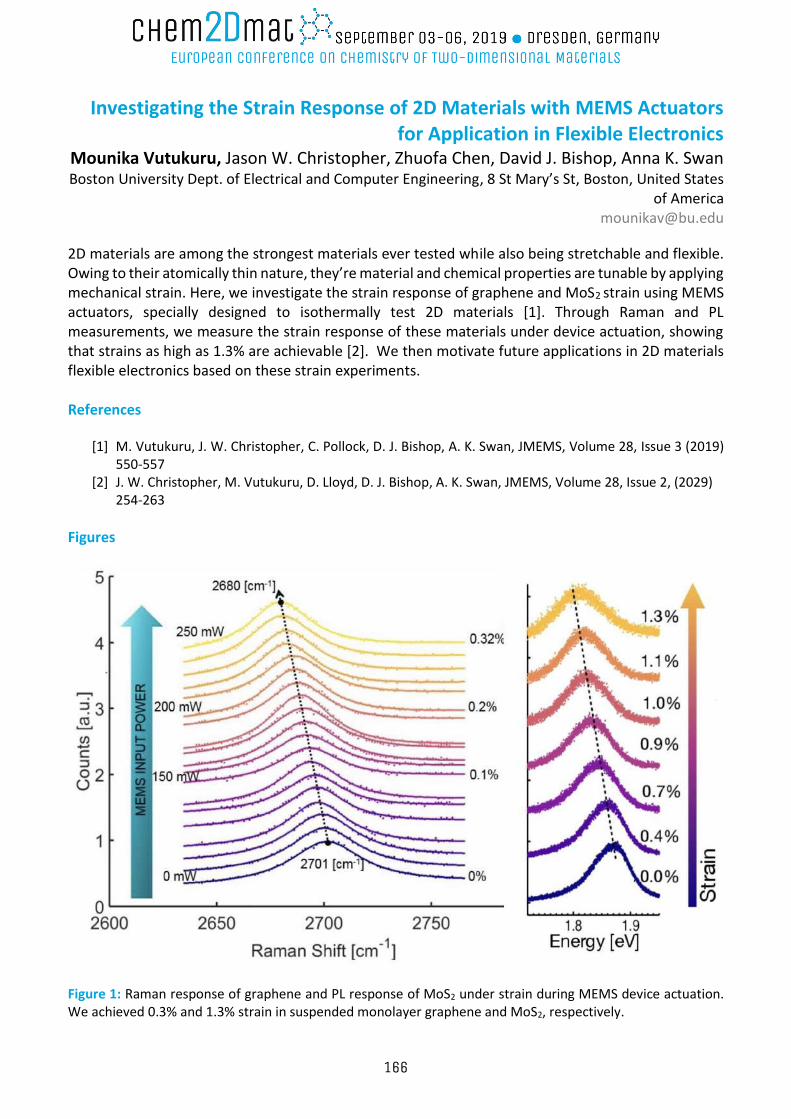
Investigating the Strain Response of 2D Materials with MEMS Actuators for Application in Flexible Electronics
Mounika Vutukuru, Jason W. Christopher, Zhuofa Chen, David J. Bishop, Anna K. Swan Boston University Dept. of Electrical and Computer Engineering, 8 St Mary’s St, Boston, United States
of America [email protected]
2D materials are among the strongest materials ever tested while also being stretchable and flexible. Owing to their atomically thin nature, they’re material and chemical properties are tunable by applying mechanical strain. Here, we investigate the strain response of graphene and MoS2 strain using MEMS actuators, specially designed to isothermally test 2D materials [1]. Through Raman and PL measurements, we measure the strain response of these materials under device actuation, showing that strains as high as 1.3% are achievable [2]. We then motivate future applications in 2D materials flexible electronics based on these strain experiments. References
[1] M. Vutukuru, J. W. Christopher, C. Pollock, D. J. Bishop, A. K. Swan, JMEMS, Volume 28, Issue 3 (2019) 550-557
[2] J. W. Christopher, M. Vutukuru, D. Lloyd, D. J. Bishop, A. K. Swan, JMEMS, Volume 28, Issue 2, (2029) 254-263
Figures
Figure 1: Raman response of graphene and PL response of MoS2 under strain during MEMS device actuation. We achieved 0.3% and 1.3% strain in suspended monolayer graphene and MoS2, respectively.
166
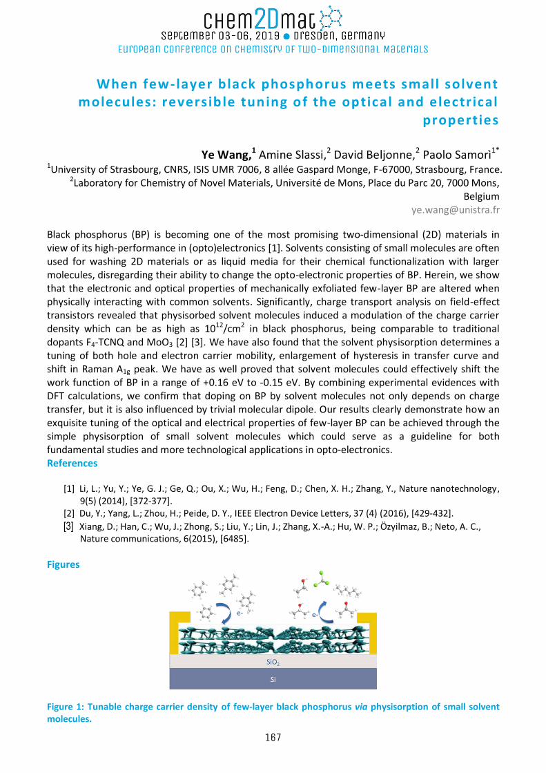
When few-layer black phosphorus meets small solvent molecules: reversib le tuning of the optical and electrical
properties
Ye Wang,1 Amine Slassi,2 David Beljonne,2 Paolo Samorì1* 1University of Strasbourg, CNRS, ISIS UMR 7006, 8 allée Gaspard Monge, F-67000, Strasbourg, France.
2Laboratory for Chemistry of Novel Materials, Université de Mons, Place du Parc 20, 7000 Mons, Belgium
Black phosphorus (BP) is becoming one of the most promising two-dimensional (2D) materials in view of its high-performance in (opto)electronics [1]. Solvents consisting of small molecules are often used for washing 2D materials or as liquid media for their chemical functionalization with larger molecules, disregarding their ability to change the opto-electronic properties of BP. Herein, we show that the electronic and optical properties of mechanically exfoliated few-layer BP are altered when physically interacting with common solvents. Significantly, charge transport analysis on field-effect transistors revealed that physisorbed solvent molecules induced a modulation of the charge carrier density which can be as high as 1012/cm2 in black phosphorus, being comparable to traditional dopants F4-TCNQ and MoO3 [2] [3]. We have also found that the solvent physisorption determines a tuning of both hole and electron carrier mobility, enlargement of hysteresis in transfer curve and shift in Raman A1g peak. We have as well proved that solvent molecules could effectively shift the work function of BP in a range of +0.16 eV to -0.15 eV. By combining experimental evidences with DFT calculations, we confirm that doping on BP by solvent molecules not only depends on charge transfer, but it is also influenced by trivial molecular dipole. Our results clearly demonstrate how an exquisite tuning of the optical and electrical properties of few-layer BP can be achieved through the simple physisorption of small solvent molecules which could serve as a guideline for both fundamental studies and more technological applications in opto-electronics. References
[1] Li, L.; Yu, Y.; Ye, G. J.; Ge, Q.; Ou, X.; Wu, H.; Feng, D.; Chen, X. H.; Zhang, Y., Nature nanotechnology, 9(5) (2014), [372-377].
[2] Du, Y.; Yang, L.; Zhou, H.; Peide, D. Y., IEEE Electron Device Letters, 37 (4) (2016), [429-432].
[3] Xiang, D.; Han, C.; Wu, J.; Zhong, S.; Liu, Y.; Lin, J.; Zhang, X.-A.; Hu, W. P.; Ö zyilmaz, B.; Neto, A. C., Nature communications, 6(2015), [6485].
Figures
Figure 1: Tunable charge carrier density of few-layer black phosphorus via physisorption of small solvent molecules.
167
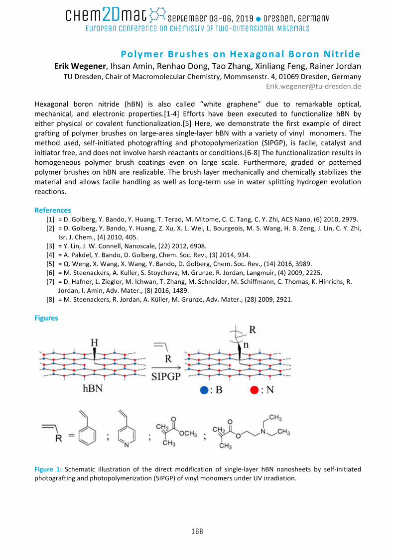
PolymerBrushesonHexagonal BoronNitr ide ErikWegener,IhsanAmin,RenhaoDong,TaoZhang,XinliangFeng,RainerJordan
TUDresden,ChairofMacromolecularChemistry,Mommsenstr.4,01069Dresden,[email protected]
Hexagonal boron nitride (hBN) is also called “white graphene” due to remarkable optical,mechanical, and electronic properties.[1-4] Efforts have been executed to functionalize hBN byeither physical or covalent functionalization.[5] Here, we demonstrate the first example of directgraftingofpolymerbrusheson large-areasingle-layerhBNwithavarietyofvinyl monomers.Themethod used, self-initiated photografting and photopolymerization (SIPGP), is facile, catalyst andinitiatorfree,anddoesnotinvolveharshreactantsorconditions.[6-8]Thefunctionalizationresultsinhomogeneous polymer brush coatings even on large scale. Furthermore, graded or patternedpolymerbrushesonhBNarerealizable.Thebrush layermechanicallyandchemicallystabilizes thematerial and allows facile handling aswell as long-termuse inwater splittinghydrogenevolutionreactions. References
[1] =D.Golberg,Y.Bando,Y.Huang,T.Terao,M.Mitome,C.C.Tang,C.Y.Zhi,ACSNano,(6)2010,2979.[2] =D.Golberg,Y.Bando,Y.Huang,Z.Xu,X.L.Wei,L.Bourgeois,M.S.Wang,H.B.Zeng,J.Lin,C.Y.Zhi,
Isr.J.Chem.,(4)2010,405.[3] =Y.Lin,J.W.Connell,Nanoscale,(22)2012,6908.[4] =A.Pakdel,Y.Bando,D.Golberg,Chem.Soc.Rev.,(3)2014,934.[5] =Q.Weng,X.Wang,X.Wang,Y.Bando,D.Golberg,Chem.Soc.Rev.,(14)2016,3989.[6] =M.Steenackers,A.Kuller,S.Stoycheva,M.Grunze,R.Jordan,Langmuir,(4)2009,2225.[7] =D.Hafner,L.Ziegler,M.Ichwan,T.Zhang,M.Schneider,M.Schiffmann,C.Thomas,K.Hinrichs,R.
Jordan,I.Amin,Adv.Mater.,(8)2016,1489.[8] =M.Steenackers,R.Jordan,A.Küller,M.Grunze,Adv.Mater.,(28)2009,2921.
Figures
Figure 1: Schematic illustration of the direct modification of single-layer hBN nanosheets by self-initiatedphotograftingandphotopolymerization(SIPGP)ofvinylmonomersunderUVirradiation.
168
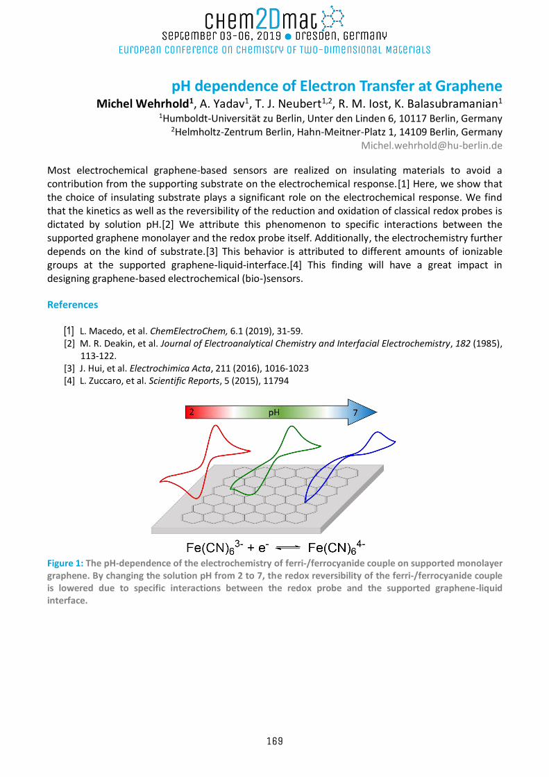
pH dependence of Electron Transfer at Graphene Michel Wehrhold1, A. Yadav1, T. J. Neubert1,2, R. M. Iost, K. Balasubramanian1
1Humboldt-Universität zu Berlin, Unter den Linden 6, 10117 Berlin, Germany 2Helmholtz-Zentrum Berlin, Hahn-Meitner-Platz 1, 14109 Berlin, Germany
[email protected] Most electrochemical graphene-based sensors are realized on insulating materials to avoid a contribution from the supporting substrate on the electrochemical response.[1] Here, we show that the choice of insulating substrate plays a significant role on the electrochemical response. We find that the kinetics as well as the reversibility of the reduction and oxidation of classical redox probes is dictated by solution pH.[2] We attribute this phenomenon to specific interactions between the supported graphene monolayer and the redox probe itself. Additionally, the electrochemistry further depends on the kind of substrate.[3] This behavior is attributed to different amounts of ionizable groups at the supported graphene-liquid-interface.[4] This finding will have a great impact in designing graphene-based electrochemical (bio-)sensors.
References
[1] L. Macedo, et al. ChemElectroChem, 6.1 (2019), 31-59. [2] M. R. Deakin, et al. Journal of Electroanalytical Chemistry and Interfacial Electrochemistry, 182 (1985),
113-122. [3] J. Hui, et al. Electrochimica Acta, 211 (2016), 1016-1023 [4] L. Zuccaro, et al. Scientific Reports, 5 (2015), 11794
Figure 1: The pH-dependence of the electrochemistry of ferri-/ferrocyanide couple on supported monolayer graphene. By changing the solution pH from 2 to 7, the redox reversibility of the ferri-/ferrocyanide couple is lowered due to specific interactions between the redox probe and the supported graphene-liquid interface.
169
Hematene for the oxygen evolution reaction: oxygen vacancy role
Yidan Wei, Mahdi Ghorbani-Asl, and Arkady V. Krasheninnikov Helmholtz-Zentrum Dresden-Rossendorf, Dresden 01328, Germany
[email protected], [email protected] and [email protected]
Abstract Using density functional theory (DFT) calculations, the catalytic activity of a recent member of two-dimensional (2D) materials, hematene (α-Fe2O3 monolayer), has been studied for oxygen evolution reactions (OER). The stability and electronic structure of two experimentally faceted sheets of hematene, (001) with anti-ferromagnetic and ferromagnetic coupling, was investigated. It was found that the isolation of bulk hematite to hematene leads to a surface energy of 1.03 J/m2 which is much higher than those for layered materials and indicates the non-van der Waals character of the exfoliated materials. The electronic structure calculations indicate that (001) facets of hematene with anti-ferromagnetic and ferromagnetic coupling are semiconducting monolayer with a band gap of about 1.06 eV and 0.6 eV, respectively. We also studied the relationship between the experimentally observed facets and their OER catalytic reactivity. In comparison to the bulk surface, hematene has a smaller OER overpotential (1.59 eV) due to the high density of surface-active sites and modified electronic structure. The presence of oxygen vacancy creates a greater number of active sites for enhancing the electrochemical OER activity and reduces the OER potential barrier from 1.39 eV to 1.28 eV. Our theoretical and experimental results provide insights for optimizing the electrocatalytic character of the naturally occurring materials for OER application.
170
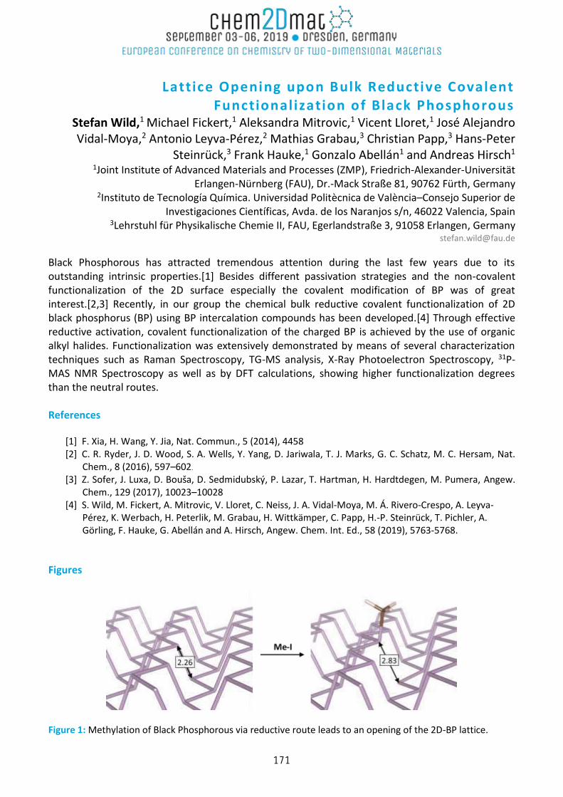
Lattice Opening upon Bulk Reductive Covalent Functionalization of Black Phosphorous
Stefan Wild,1 Michael Fickert,1 Aleksandra Mitrovic,1 Vicent Lloret,1 José Alejandro Vidal-Moya,2 Antonio Leyva-Pérez,2 Mathias Grabau,3 Christian Papp,3 Hans-Peter
Steinrück,3 Frank Hauke,1 Gonzalo Abellán1 and Andreas Hirsch1 1Joint Institute of Advanced Materials and Processes (ZMP), Friedrich-Alexander-Universität
Erlangen-Nürnberg (FAU), Dr.-Mack Straße 81, 90762 Fürth, Germany 2Instituto de Tecnologia Quimica. Universidad Politecnica de Valencia–Consejo Superior de
Investigaciones Cientificas, Avda. de los Naranjos s/n, 46022 Valencia, Spain 3Lehrstuhl für Physikalische Chemie II, FAU, Egerlandstraße 3, 91058 Erlangen, Germany
Black Phosphorous has attracted tremendous attention during the last few years due to its outstanding intrinsic properties.[1] Besides different passivation strategies and the non-covalent functionalization of the 2D surface especially the covalent modification of BP was of great interest.[2,3] Recently, in our group the chemical bulk reductive covalent functionalization of 2D black phosphorus (BP) using BP intercalation compounds has been developed.[4] Through effective reductive activation, covalent functionalization of the charged BP is achieved by the use of organic alkyl halides. Functionalization was extensively demonstrated by means of several characterization techniques such as Raman Spectroscopy, TG-MS analysis, X-Ray Photoelectron Spectroscopy, 31P-MAS NMR Spectroscopy as well as by DFT calculations, showing higher functionalization degrees than the neutral routes. References
[1] F. Xia, H. Wang, Y. Jia, Nat. Commun., 5 (2014), 4458 [2] C. R. Ryder, J. D. Wood, S. A. Wells, Y. Yang, D. Jariwala, T. J. Marks, G. C. Schatz, M. C. Hersam, Nat.
Chem., 8 (2016), 597–602. [3] Z. Sofer, J. Luxa, D. Bouša, D. Sedmidubský, P. Lazar, T. Hartman, H. Hardtdegen, M. Pumera, Angew.
Chem., 129 (2017), 10023–10028 [4] S. Wild, M. Fickert, A. Mitrovic, V. Lloret, C. Neiss, J. A. Vidal-Moya, M. Á. Rivero-Crespo, A. Leyva-
Pérez, K. Werbach, H. Peterlik, M. Grabau, H. Wittkämper, C. Papp, H.-P. Steinrück, T. Pichler, A. Görling, F. Hauke, G. Abellán and A. Hirsch, Angew. Chem. Int. Ed., 58 (2019), 5763-5768.
Figures
Figure 1: Methylation of Black Phosphorous via reductive route leads to an opening of the 2D-BP lattice.
171
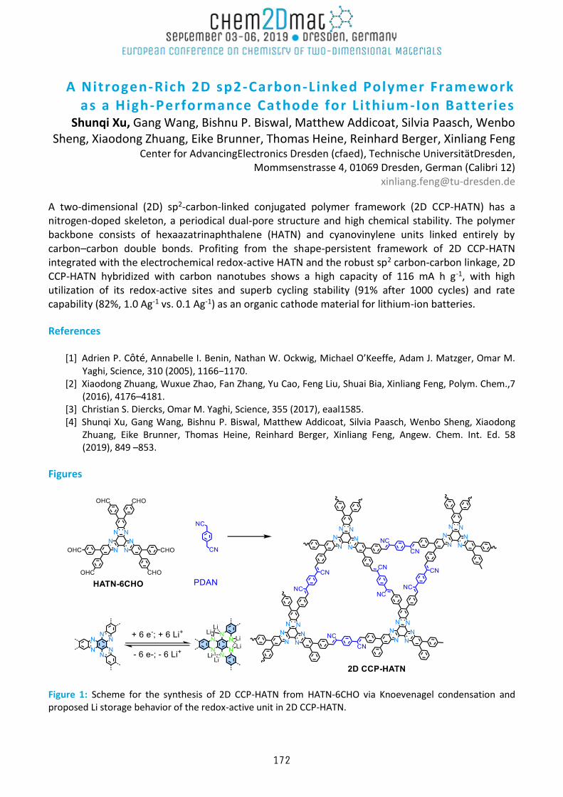
A Nitrogen-Rich 2D sp2-Carbon-Linked Polymer Framework as a High-Performance Cathode for Li thium -Ion Batteries
Shunqi Xu, Gang Wang, Bishnu P. Biswal, Matthew Addicoat, Silvia Paasch, Wenbo Sheng, Xiaodong Zhuang, Eike Brunner, Thomas Heine, Reinhard Berger, Xinliang Feng
Center for AdvancingElectronics Dresden (cfaed), Technische UniversitätDresden, Mommsenstrasse 4, 01069 Dresden, German (Calibri 12)
A two-dimensional (2D) sp2-carbon-linked conjugated polymer framework (2D CCP-HATN) has a nitrogen-doped skeleton, a periodical dual-pore structure and high chemical stability. The polymer backbone consists of hexaazatrinaphthalene (HATN) and cyanovinylene units linked entirely by carbon–carbon double bonds. Profiting from the shape-persistent framework of 2D CCP-HATN integrated with the electrochemical redox-active HATN and the robust sp2 carbon-carbon linkage, 2D CCP-HATN hybridized with carbon nanotubes shows a high capacity of 116 mA h g-1, with high utilization of its redox-active sites and superb cycling stability (91% after 1000 cycles) and rate capability (82%, 1.0 Ag-1 vs. 0.1 Ag-1) as an organic cathode material for lithium-ion batteries.
References
[1] Adrien P. Côté, Annabelle I. Benin, Nathan W. Ockwig, Michael O’Keeffe, Adam J. Matzger, Omar M. Yaghi, Science, 310 (2005), 1166−1170.
[2] Xiaodong Zhuang, Wuxue Zhao, Fan Zhang, Yu Cao, Feng Liu, Shuai Bia, Xinliang Feng, Polym. Chem.,7 (2016), 4176–4181.
[3] Christian S. Diercks, Omar M. Yaghi, Science, 355 (2017), eaal1585. [4] Shunqi Xu, Gang Wang, Bishnu P. Biswal, Matthew Addicoat, Silvia Paasch, Wenbo Sheng, Xiaodong
Zhuang, Eike Brunner, Thomas Heine, Reinhard Berger, Xinliang Feng, Angew. Chem. Int. Ed. 58 (2019), 849 –853.
Figures
Figure 1: Scheme for the synthesis of 2D CCP-HATN from HATN-6CHO via Knoevenagel condensation and proposed Li storage behavior of the redox-active unit in 2D CCP-HATN.
172
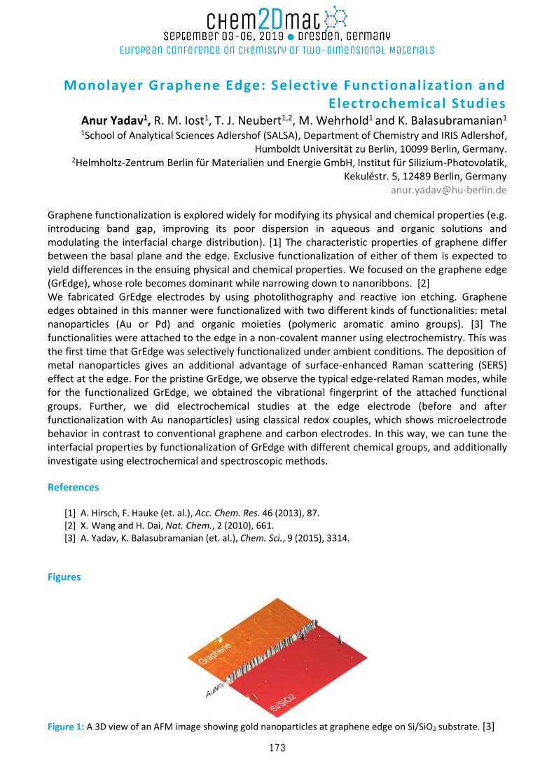
Monolayer Graphene Edge: Select ive Functional izat ion and Electrochemical Studies
Anur Yadav1, R. M. Iost1, T. J. Neubert1,2, M. Wehrhold1 and K. Balasubramanian1 1School of Analytical Sciences Adlershof (SALSA), Department of Chemistry and IRIS Adlershof,
Humboldt Universität zu Berlin, 10099 Berlin, Germany. 2Helmholtz-Zentrum Berlin für Materialien und Energie GmbH, Institut für Silizium-Photovolatik,
Kekuléstr. 5, 12489 Berlin, Germany [email protected]
Graphene functionalization is explored widely for modifying its physical and chemical properties (e.g. introducing band gap, improving its poor dispersion in aqueous and organic solutions and modulating the interfacial charge distribution). [1] The characteristic properties of graphene differ between the basal plane and the edge. Exclusive functionalization of either of them is expected to yield differences in the ensuing physical and chemical properties. We focused on the graphene edge (GrEdge), whose role becomes dominant while narrowing down to nanoribbons. [2] We fabricated GrEdge electrodes by using photolithography and reactive ion etching. Graphene edges obtained in this manner were functionalized with two different kinds of functionalities: metal nanoparticles (Au or Pd) and organic moieties (polymeric aromatic amino groups). [3] The functionalities were attached to the edge in a non-covalent manner using electrochemistry. This was the first time that GrEdge was selectively functionalized under ambient conditions. The deposition of metal nanoparticles gives an additional advantage of surface-enhanced Raman scattering (SERS) effect at the edge. For the pristine GrEdge, we observe the typical edge-related Raman modes, while for the functionalized GrEdge, we obtained the vibrational fingerprint of the attached functional groups. Further, we did electrochemical studies at the edge electrode (before and after functionalization with Au nanoparticles) using classical redox couples, which shows microelectrode behavior in contrast to conventional graphene and carbon electrodes. In this way, we can tune the interfacial properties by functionalization of GrEdge with different chemical groups, and additionally investigate using electrochemical and spectroscopic methods.
References
[1] A. Hirsch, F. Hauke (et. al.), Acc. Chem. Res. 46 (2013), 87. [2] X. Wang and H. Dai, Nat. Chem., 2 (2010), 661. [3] A. Yadav, K. Balasubramanian (et. al.), Chem. Sci., 9 (2015), 3314.
Figures
Figure 1: A 3D view of an AFM image showing gold nanoparticles at graphene edge on Si/SiO2 substrate. [3]
173
Electrochemical Energy Storage using Graphene Materia ls in Water- In-Salt Based Electrolyte (WiSE)
Zahid Ali Zafar, Martin Silhavik, Jiri Cervenka Department of Thin Films and Nanostructures, FZU – Institute of Physics of The Czech Academy of
Sciences, Prague 16200, Czech Republic [email protected]
Energy storage systems based on aqueous electrolytes offer higher safety and lower costs. Nevertheless, their biggest bottleneck is the narrow electrochemical window (1.23V) that is preventing from attaining higher energy and power densities in most of the aqueous electrochemical energy storage devices. For instance, aqueous rechargeable aluminum ion batteries promise high energy density due to multivalent redox chemistry of aluminum ion (Al3+) but they exhibit much lower energy density in real experiments due to the limited electrochemical windows of the aqueous electrolytes. The water-in-salt based electrolytes (WiSE) can potentially eliminate this barrier by offering a larger electrochemical window by reducing the overall electrochemical activity of water on the electrodes. Here, we demonstrate a new concept using aluminum perchlorate based WiSE that is showing a stable and wide electrochemical window of nearly 3 V against Ag/AgCl. The electrochemistry tests of the electrolyte are performed using Kish graphite and hydrothermally reduced graphene electrodes. We employ the new electrochemical system in aqueous rechargeable aluminum ion batteries and supercapacitors, revealing superior performance to standard aqueous electrolytes. Our findings provide new possibilities for enhancing the electrochemical window and enhancing the energy and power density in aqueous electrochemical energy storage systems.
References
[1] L. Smith, B. Dunn, Science, 6263 (2015) 918. [2] Z.A. Zafar, S. Imtiaz, R. Razaq, S. Ji, T. Huang, Z. Zhang, Y. Huang, J.A. Anderson, Journal of Materials
Chemistry A, 12 (2017) 5646-5660. [3] Q. Dou, Y. Lu, L. Su, X. Zhang, S. Lei, X. Bu, L. Liu, D. Xiao, J. Chen, S. Shi, X. Yan, Energy Storage
Materials (2019) [4] M. Kazazi, Z.A. Zafar, M. Delshad, J. Cervenka, C. Chen, Solid State Ionics, 320 (2018) 64-69.
174
Fluorine-free Bottom-up Strategy for the Synthesis of 2D TiO 2 Anatase
Marco Zarattini1, Alexandre Felten2, Liam Isherwood1, Jarrid Wittkopf3, Robert Cri Ionescu3, Helen Holder3*, Cinzia Casiraghi1*
1The University of Manchester, Oxford Road, Manchester, United Kingdom 2Université de Namur ASBL, Rue de Bruxelles 61, Namur, Belgium
3HP Labs, Page Mill Road 1501, Palo Alto, United States of America [email protected]
Titanium oxide (TiO2) is an inorganic compound that belongs to the wide group of d-metal oxides TMOs, which has been widely studied over the past few decades due to its low cost, chemical stability, non-toxicity, allowing its use in photocatalysis, electronics and biomedical applications [1], to give a few examples. TiO2 exists in different polymorphs of which Anatase (tetragonal, l41/amd), Rutile (tetragonal, P42/mnm), Brookite (orthorhombic, Pbca) and TiO2 (B) (monoclinic, C2/m) are the most commonly investigated structures. Among the four different crystalline phases of TiO2, Anatase TiO2 has been widely accepted to possess the most photoactive reactivity in catalytic applications [2]. 2D TiO2 Anatase has been shown to have even better photocatalytic performance due to its dimensionality, which gives rise to higher surface to volume ratio [3]. One of the most used strategies for the synthesis of 2D TiO2 Anatase is based on the use of a hydrothermal route, employing hydrofluoric acid (HF) as a capping agent [4]. Although the synthetic procedure is highly efficient, it involves the use of HF which is known to be highly corrosive and toxic. In this work we use a novel fluorine-free bottom-up strategy to synthesize 2D TiO2 Anatase. The material has been fully characterized by X-ray diffraction (XRD), X-ray photoelectron spectroscopy (XPS), atomic force microscopy (AFM), transmission electron microscopy (TEM) and Raman spectroscopy. We show that the material has a two-dimensional morphology with high degree of crystallinity which is useful for photocatalysis applications. References
[1] L. Wang et. al, Chemical Reviews 114 (2014) 9455-9486
[2] W.J. Ong et. al, Nanoscale 6 (2014) 1946-2008
[3] A. Selloni, Nature Materials 7 (2008) 613-615
[4] H.G. Yang et. al, Nature 453 (2008) 638-642
175