Embed Size (px)
Citation preview
1
Chemical Bonding Transformation Mapping to Optimize Low-k Dielectric Nanostructure Fabrication and Post-etch
Residue Clean
Oliver Chyan*, Sirish Rimal, Tamal Mukherjee,
Muthappan Asokan, Seare A. Berhe
Interfacial Electrochemistry and Materials Research Lab, University of North Texas
Present to SPCC-2017, *[email protected]
Kanwaljit Singh
Components Research, Intel Corporation
Ian Brown, Jacques Faguet
US-Technology Development Center, TEL Technology Center

2
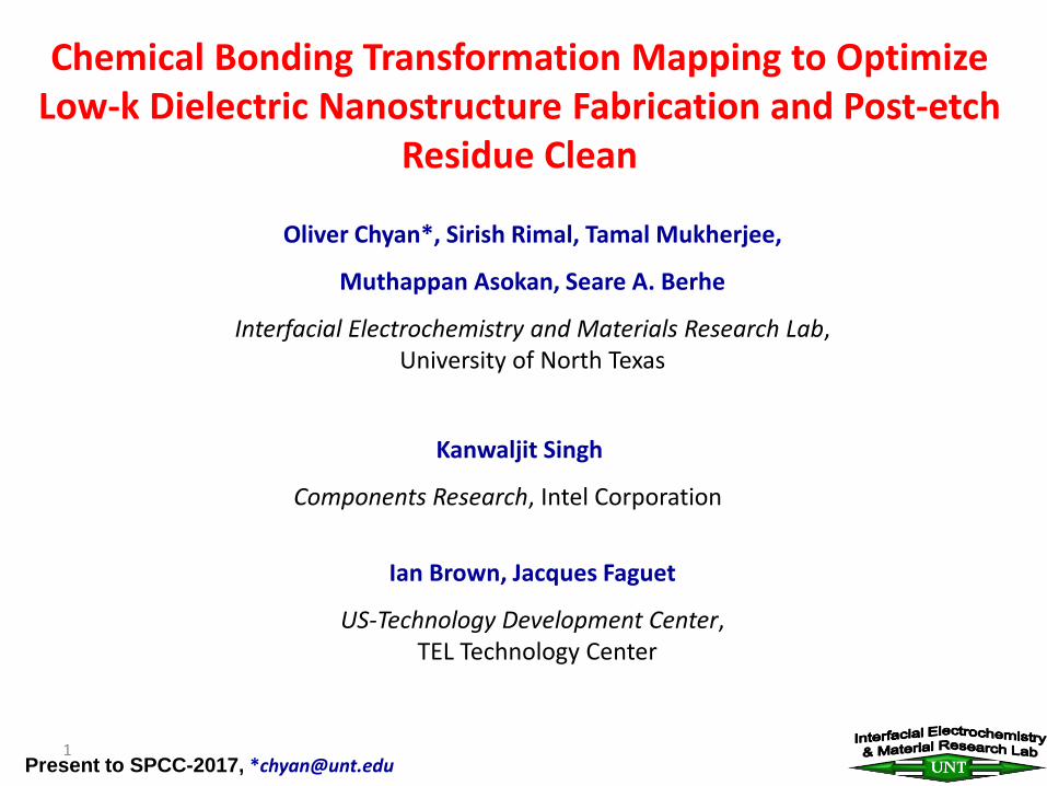
Goal: Explore the underlying fundamental science that leads to real engineering solutions for important interfacial issues in
microelectronic fabrication.
Group members:
Alex Lambert, Issac Goutham, Muthappan Asokan, Seare Berhe
Alumni :
Dr. Sirish Rimal (JSR-Micro)
Dr. Tamal Mukherjee (LAM)
Dr. Nick Ross (Intel)
Dr. Kyle Yu (TEL)
Dr. Karthik Pillai (TEL)
Dr. Simon Koskey (Intel) 3
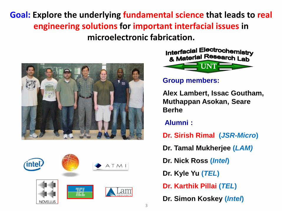
Interfacial Electrochemistry & Materials Research Lab
Front end (FEOL): Silicon surface preparation, H-passivation, SC1/SC2 cleaning, Silicon oxide etching, metal (Cu) and organic contamination control/detection.
"An Apparatus and Method for Detecting Impurities in Wet Chemicals " U.S. Patent 6145372, 2000.
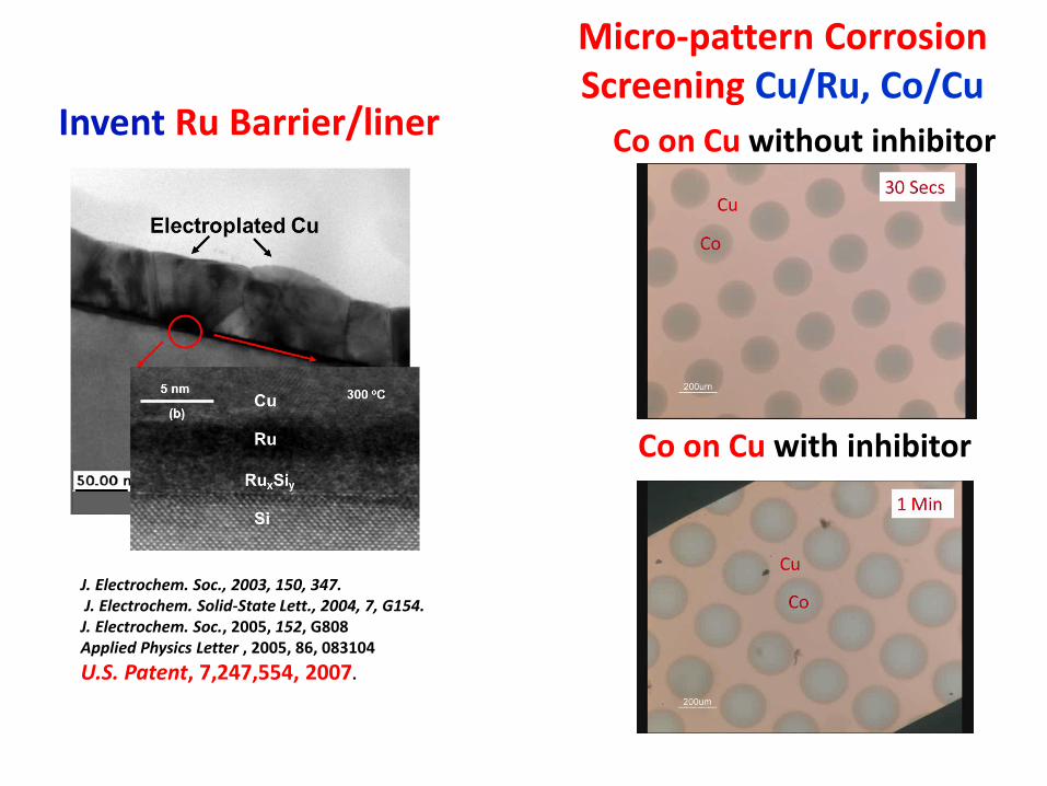
Back end (BEOL): Cu ECD, Ru-based liner/barrier, Cu cleaning chemistry, Cu bimetallic corrosion mechanism, Post etch residue, Porous Low-k damage control.
"Method of Making Integrated Circuits Using Ruthenium and Its Oxides as Cu Diffusion Barrier", U.S. Patent 7247554, 2007.
IC Packaging: Cu vs. Au wire bonded device, Al pad corrosion prevention, molding compounds, Subtractive Cu Etching.
“Systems and Methods for Copper Etch Monitoring and Control", U.S. Patent Application, 2016.
“Method for Wafer Characterization", U.S. Patent 9366601, 2016.
(1992-2002)
(2000 - Date)
(2015 - Date)
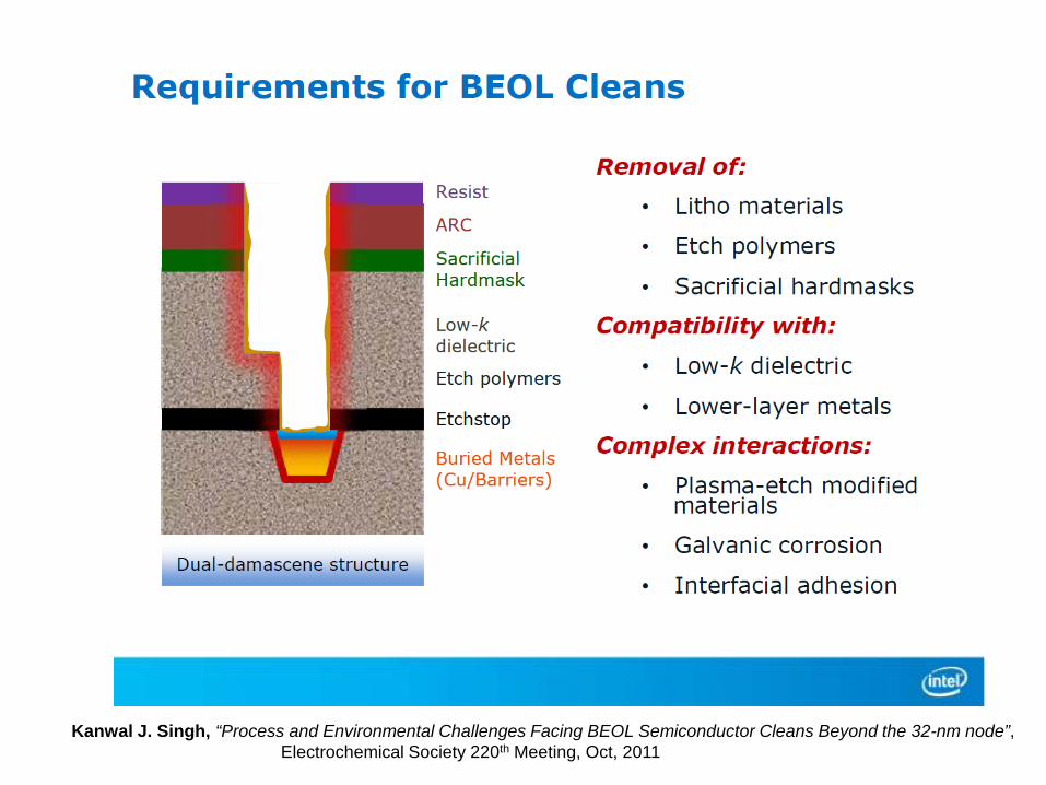
Kanwal J. Singh, “Process and Environmental Challenges Facing BEOL Semiconductor Cleans Beyond the 32-nm node”, Electrochemical Society 220th Meeting, Oct, 2011
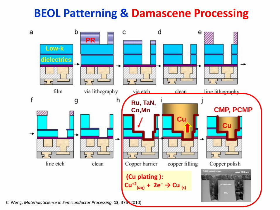
C. Weng, Materials Science in Semiconductor Processing, 13, 376 (2010)
BEOL Patterning & Damascene Processing
(Cu plating ): Cu+2
(aq) + 2e− → Cu (s)
Cu Cu
Low-k
dielectrics
CMP, PCMP
PR
Ru, TaN, Co,Mn
Micro-pattern Corrosion Screening Cu/Ru, Co/Cu
Co on Cu without inhibitor
Co on Cu with inhibitor
J. Electrochem. Soc., 2003, 150, 347. J. Electrochem. Solid-State Lett., 2004, 7, G154. J. Electrochem. Soc., 2005, 152, G808 Applied Physics Letter , 2005, 86, 083104 U.S. Patent, 7,247,554, 2007.
Invent Ru Barrier/liner
C. Weng, Materials Science in Semiconductor Processing, 13, 376 (2010) 8
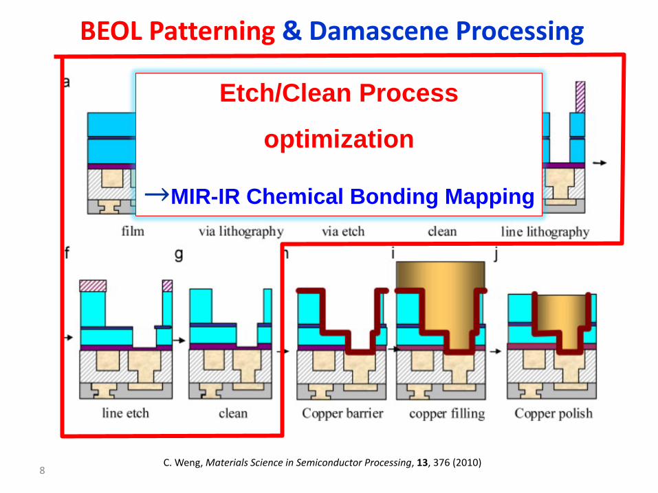
BEOL Patterning & Damascene Processing
Etch/Clean Process
optimization
→MIR-IR Chemical Bonding Mapping
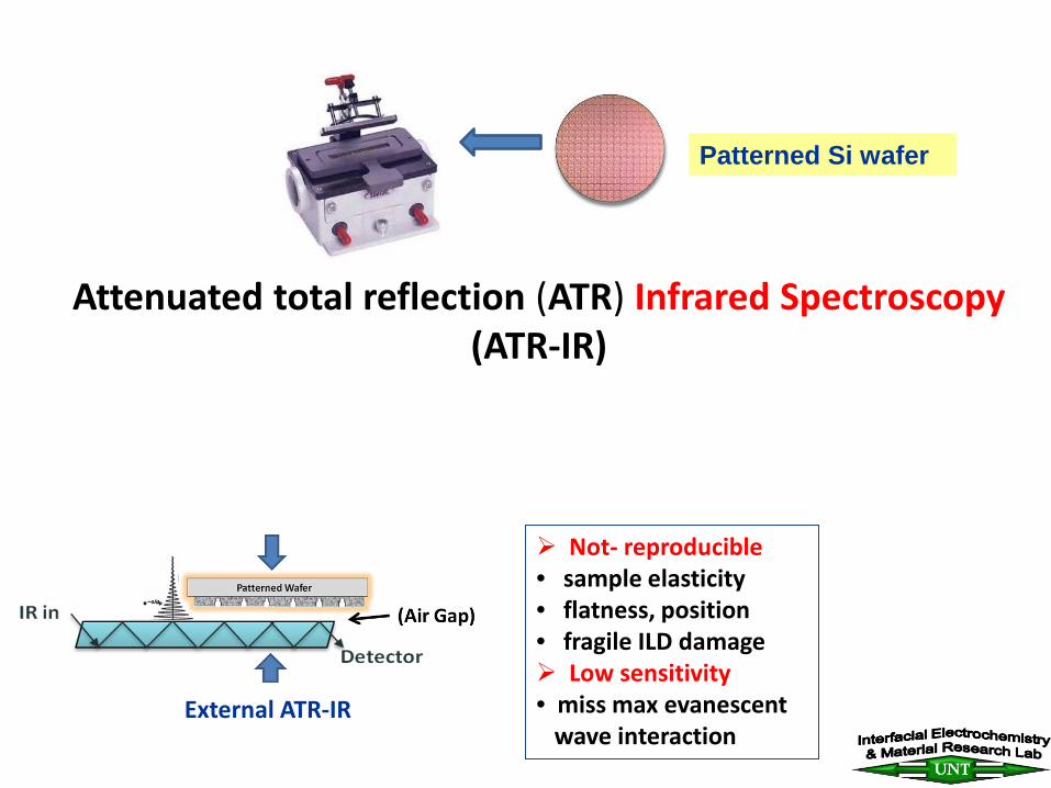
Attenuated total reflection (ATR) Infrared Spectroscopy (ATR-IR)
External ATR-IR
Not- reproducible • sample elasticity • flatness, position • fragile ILD damage Low sensitivity • miss max evanescent wave interaction
Patterned Si wafer
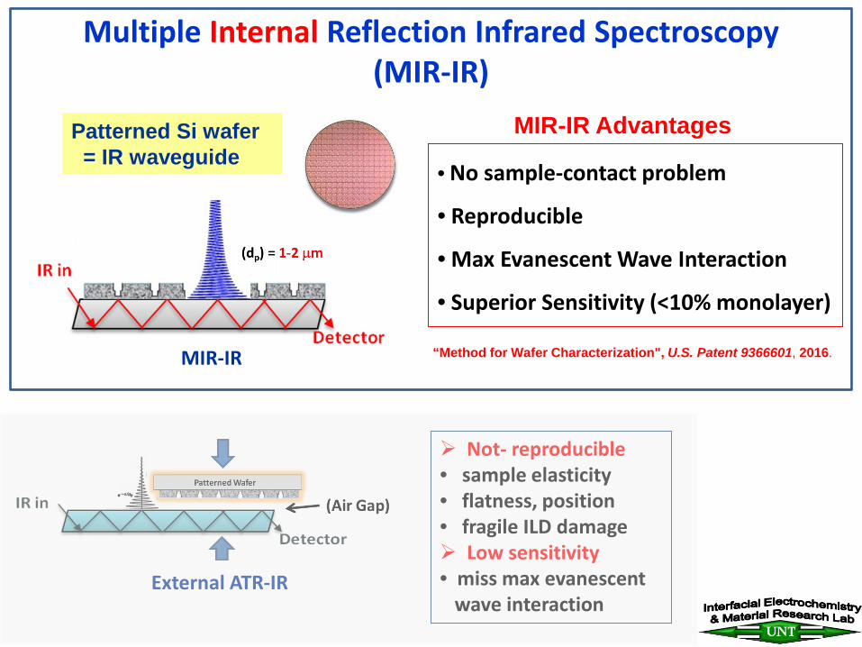
• No sample-contact problem
• Reproducible
• Max Evanescent Wave Interaction
• Superior Sensitivity (<10% monolayer)
Multiple Internal Reflection Infrared Spectroscopy (MIR-IR)
MIR-IR Advantages Patterned Si wafer = IR waveguide
“Method for Wafer Characterization", U.S. Patent 9366601, 2016. MIR-IR
External ATR-IR
Not- reproducible • sample elasticity • flatness, position • fragile ILD damage Low sensitivity • miss max evanescent wave interaction
11
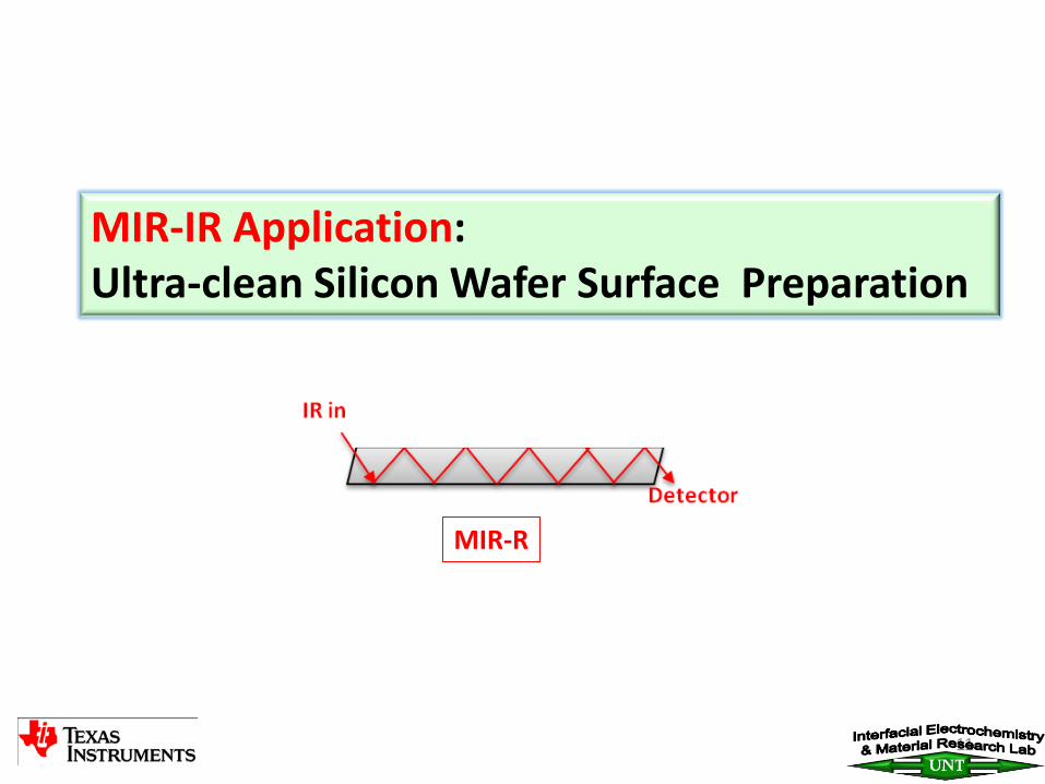
MIR-IR Application: Ultra-clean Silicon Wafer Surface Preparation
MIR-R
O-SiHx
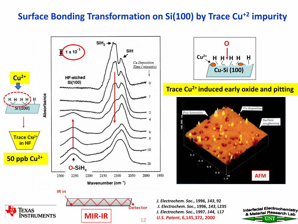
Surface Bonding Transformation on Si(100) by Trace Cu+2 impurity
12 MIR-IR
50 ppb Cu2+
J. Electrochem. Soc., 1996, 143, 92 J. Electrochem. Soc., 1996, 143, L235 J. Electrochem. Soc., 1997, 144, L17 U.S. Patent, 6,145,372, 2000
H
Cu-Si (100)
H H H H Cu2+
O
Trace Cu2+ induced early oxide and pitting
AFM
Cu2+
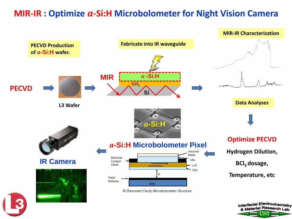
Optimize PECVD
Hydrogen Dilution,
BCl3 dosage,
Temperature, etc
𝒂𝒂-Si:H Microbolometer Pixel
IR Camera
MIR-IR : Optimize 𝒂𝒂-Si:H Microbolometer for Night Vision Camera
PECVD
Fabricate into IR waveguide
MIR-IR Characterization
Data Analyses L3 Wafer
PECVD Production of 𝒂𝒂-Si:H wafer.
SiNx
𝒂𝒂 -Si:H
Si
MIR
𝒂𝒂-Si:H
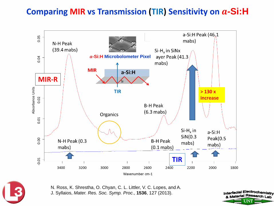
Comparing MIR vs Transmission (TIR) Sensitivity on 𝒂𝒂-Si:H
N. Ross, K. Shrestha, O. Chyan, C. L. Littler, V. C. Lopes, and A. J. Syllaios, Mater. Res. Soc. Symp. Proc., 1536, 127 (2013).
𝒂𝒂-Si:H Microbolometer Pixel
MIR-R
TIR
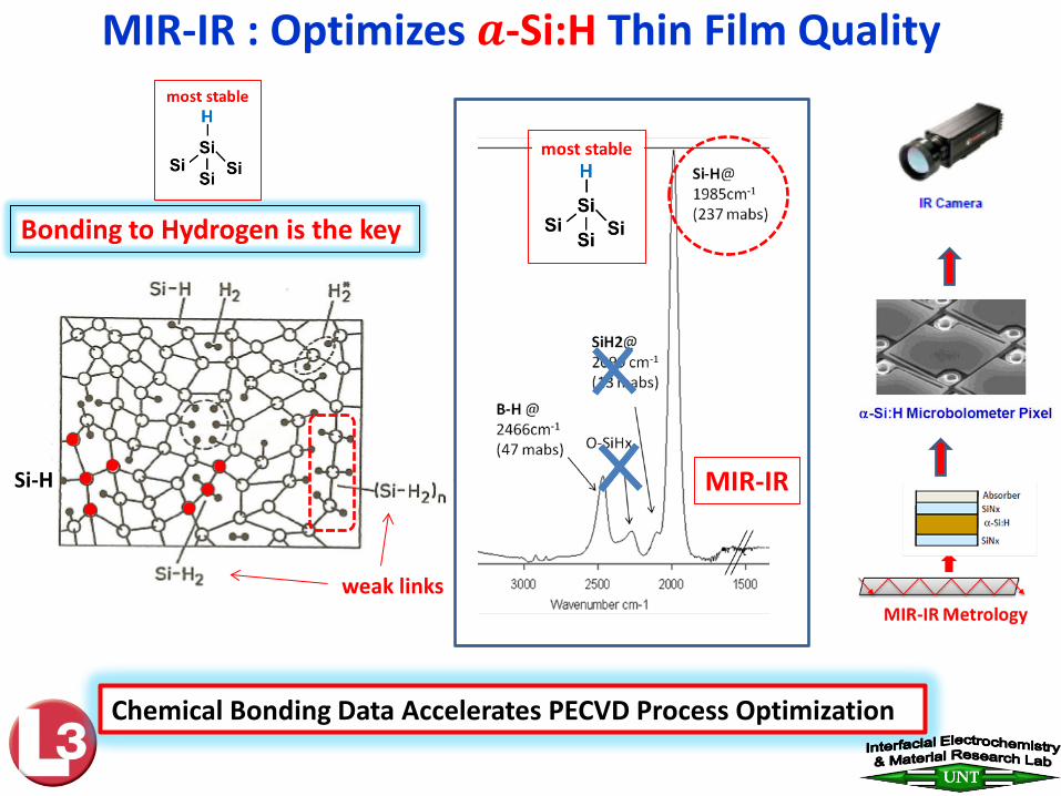
weak links
Si-H
MIR-IR : Optimizes 𝒂𝒂-Si:H Thin Film Quality
Bonding to Hydrogen is the key
Chemical Bonding Data Accelerates PECVD Process Optimization
MIR-IR
16
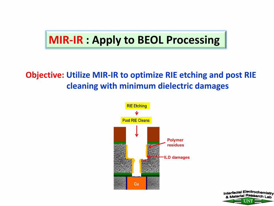
MIR-IR : Apply to BEOL Processing
Objective: Utilize MIR-IR to optimize RIE etching and post RIE cleaning with minimum dielectric damages
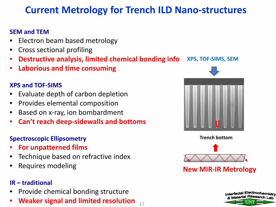
SEM and TEM • Electron beam based metrology • Cross sectional profiling • Destructive analysis, limited chemical bonding info • Laborious and time consuming XPS and TOF-SIMS • Evaluate depth of carbon depletion • Provides elemental composition • Based on x-ray, ion bombardment • Can’t reach deep-sidewalls and bottoms Spectroscopic Ellipsometry • For unpatterned films • Technique based on refractive index • Requires modeling
IR – traditional • Provide chemical bonding structure • Weaker signal and limited resolution 17
Trench bottom
XPS, TOF-SIMS, SEM
New MIR-IR Metrology
Current Metrology for Trench ILD Nano-structures
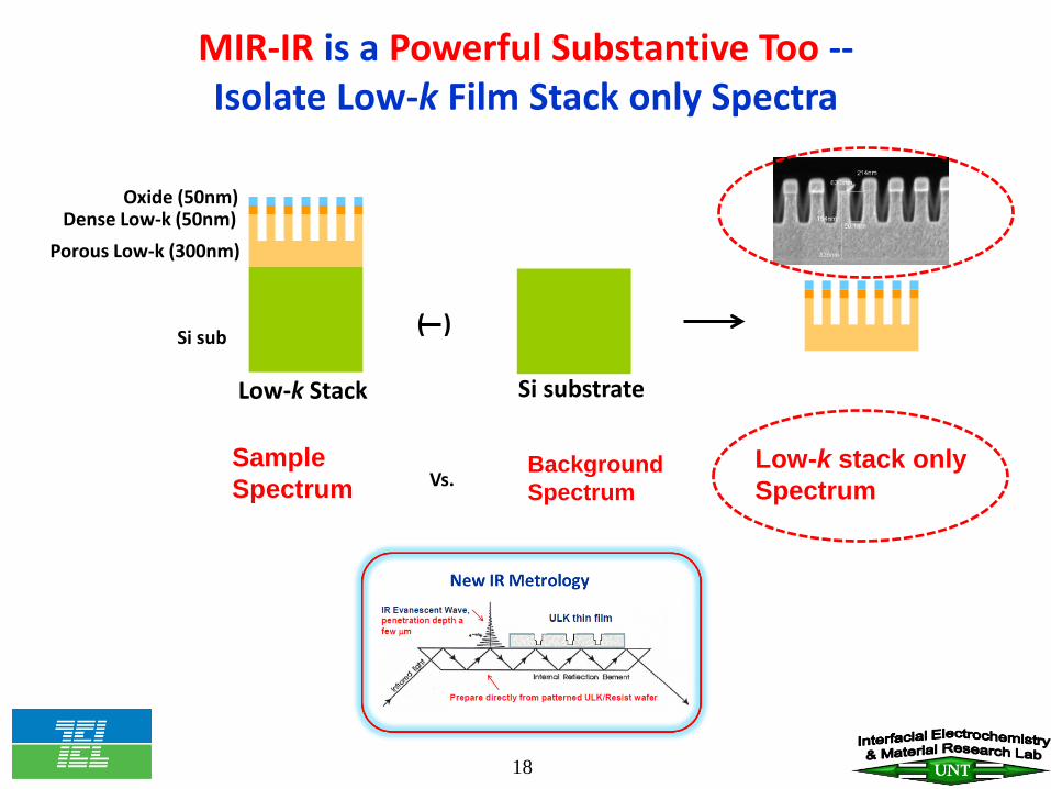
MIR-IR is a Powerful Substantive Too -- Isolate Low-k Film Stack only Spectra
Si sub
Porous Low-k (300nm) Dense Low-k (50nm)
Oxide (50nm)
Low-k Stack
Sample Spectrum
Background Spectrum
Si substrate
Vs.
( )
Low-k stack only Spectrum
18
Abso
rban
ce
Wavenumber cm-1
Si-OH
a-CH3
CH2
SiHx O-SiHx
Si-CH3 (bend)
Si-O cage Si-O
network
Si-CH3 (rock
Low-k Damage
Carbon Doping
Carbon Doping
Low-k
Low-k damage
Residue removal
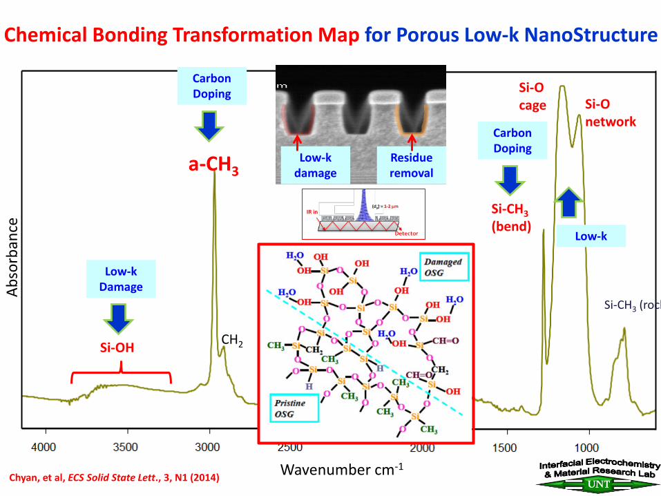
Chyan, et al, ECS Solid State Lett., 3, N1 (2014)
Chemical Bonding Transformation Map for Porous Low-k NanoStructure
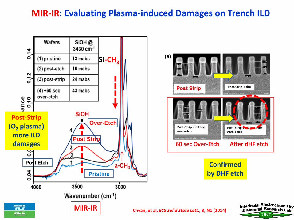
MIR-IR: Evaluating Plasma-induced Damages on Trench ILD
Chyan, et al, ECS Solid State Lett., 3, N1 (2014)
Post Strip
Over-Etch
Si-CH3
MIR-IR
Post Etch
Pristine Confirmed
by DHF etch
Post-Strip (O2 plasma)
more ILD damages
2400 2600 2800 3000 3200 3400 3600 3800 4000
Wavenumber (cm-1)
0.02
0.
04
0.06
0.
08
0.10
0.
12
0.14
Abso
rban
ce
Strip 1 Strip 2 Strip 3 Strip 4
a-CH3
Si-OH
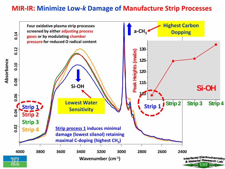
MIR-IR: Minimize Low-k Damage of Manufacture Strip Processes
Four oxidative plasma strip processes screened by either adjusting process gases or by modulating chamber pressure for reduced O radical content
Strip process 1 induces minimal damage (lowest silanol) retaining maximal C-doping (highest CH3)
Strip 1 Strip 2 Strip 3 Strip 4
110
115
120
125
130
Peak
Hei
ghts
(mab
s)
Si-OH
Strip 1 Lowest Water Sensitivity
Highest Carbon Dopping
Abso
rban
ce
Wavenumber cm-1
Si-OH
a-CH3
CH2
SiHx O-SiHx
Si-CH3 (bend)
Si-O cage Si-O
network
Si-CH3 (rock
Low-k Damage
Carbon Doping
Carbon Doping
FC=CF
C=CF
C=C
CH3, CH2, CH (def.)
Etch residue Low-k
Low-k damage
Residue removal
Chemical Bonding Transformation Map for Porous Low-k NanoStructure
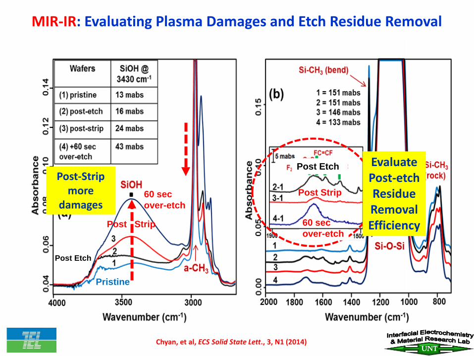
MIR-IR: Evaluating Plasma Damages and Etch Residue Removal
Pristine
Post Etch
Post Strip
60 sec over-etch
Post-Strip more
damages
Evaluate Post-etch Residue Removal Efficiency
Chyan, et al, ECS Solid State Lett., 3, N1 (2014)
60 sec over-etch
Post Strip
Post Etch
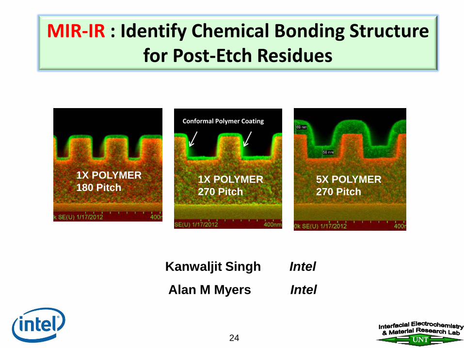
1X POLYMER 270 Pitch
Conformal Polymer Coating
1X POLYMER 180 Pitch
5X POLYMER 270 Pitch
Kanwaljit Singh Intel
Alan M Myers Intel
24
MIR-IR : Identify Chemical Bonding Structure for Post-Etch Residues
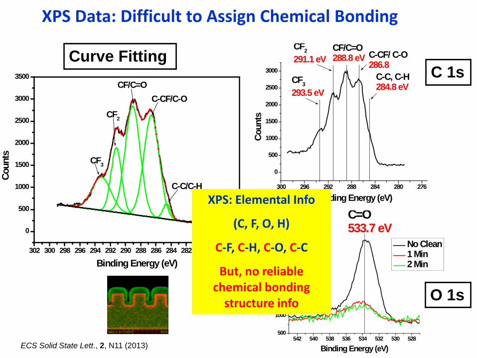
XPS Data: Difficult to Assign Chemical Bonding
542 540 538 536 534 532 530 528500
1000
1500
2000
2500
3000
3500
C=O533.7 eV
Coun
ts
Binding Energy (eV)
No Clean 1 Min 2 Min
300 296 292 288 284 280 276
0
500
1000
1500
2000
2500
3000CF3293.5 eV
CF2
291.1 eVCF/C=O288.8 eV C-CF/ C-O
286.8C-C, C-H284.8 eV
Coun
ts
Binding Energy (eV)
C 1s Curve Fitting
O 1s
302 300 298 296 294 292 290 288 286 284 282 280 278 276
0
500
1000
1500
2000
2500
3000
3500
CF3
CF2
CF/C=OC-CF/C-O
C-C/C-H
Coun
ts
Binding Energy (eV)
ECS Solid State Lett., 2, N11 (2013)
XPS: Elemental Info
(C, F, O, H)
C-F, C-H, C-O, C-C
But, no reliable chemical bonding
structure info
2000 1600 1200 800
Abso
rban
ce (a
.u.)
Wavenumber (cm-1)
1x 5x
. (CF2)
def (am)
. . (CF2)s
(CF2)as
. CF3i . . . .
C=CF F2C=CF C=O
FC=CF
. CF3
t
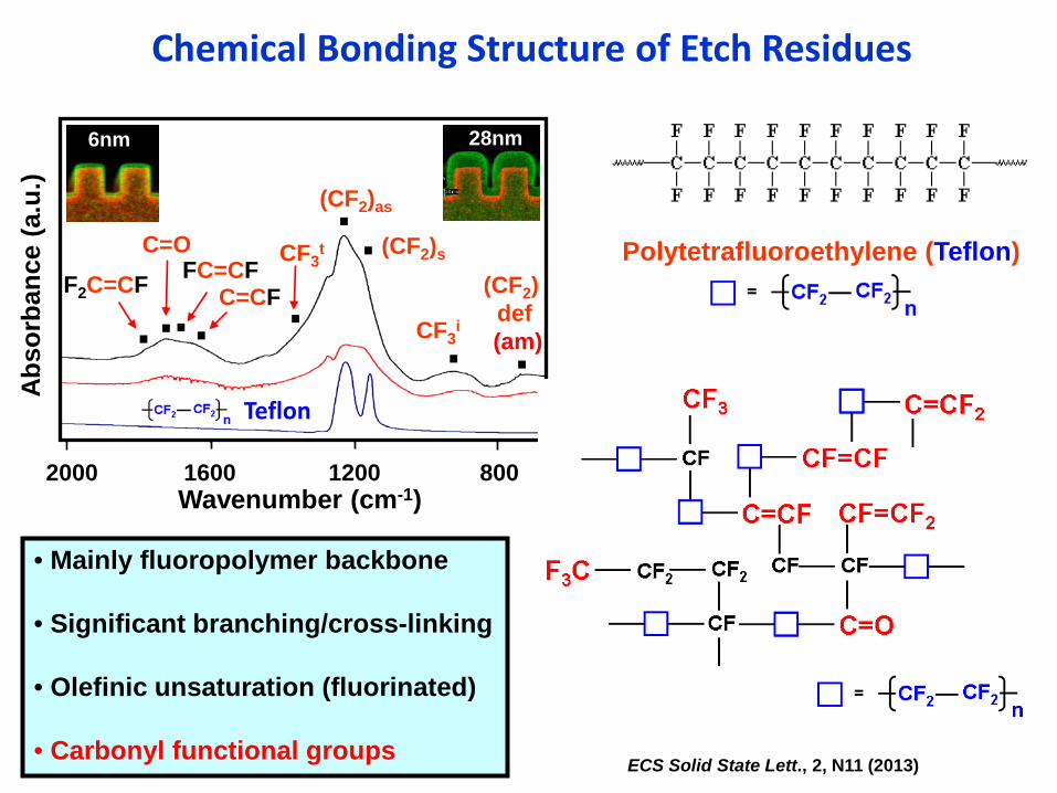
• Mainly fluoropolymer backbone
• Significant branching/cross-linking
• Olefinic unsaturation (fluorinated)
• Carbonyl functional groups
Polytetrafluoroethylene (Teflon)
6nm 28nm
Chemical Bonding Structure of Etch Residues
ECS Solid State Lett., 2, N11 (2013)
Teflon
FC
CF2
FC
CF
CF2CF2
CFC
F2F2C
CF2
FCF2C
CF
F2C CF2
FC
F2C CF2
CF
C
F2C
F2C
CCF2
O
H3C
C
F2C CF2 FC CF2
CF2
FC
CF2
CF2
F2C
n
n
CF2
FC F
C
F2CFC
F2C
F2C CF2
CFCF2
CF2
n
COO
n
n
n
n
nn
CF3F2C
CF2
F2C
CF3
F2C
n
F2Cn
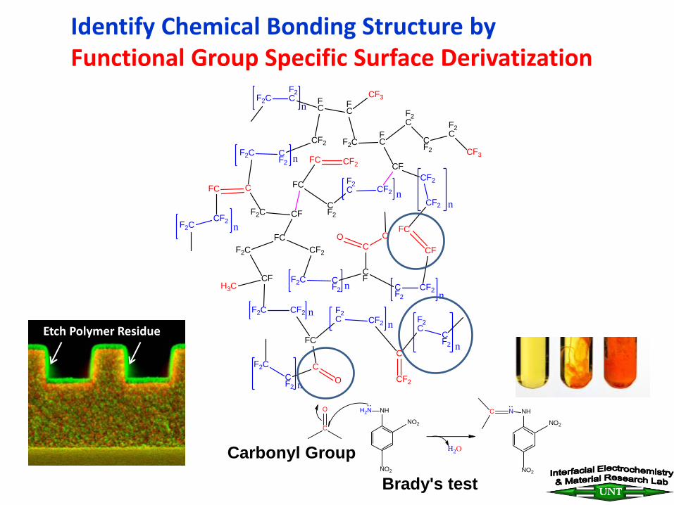
Identify Chemical Bonding Structure by Functional Group Specific Surface Derivatization
Etch Polymer Residue
C
O NHH2N
NO2
NO2
NHN
NO2
NO2
C
H2O
Brady's test
Carbonyl Group
1710
C
O NHH2N
NO2
NO2
NHN
NO2
NO2
C
H2OFC
CF2
FC
CF
CF2CF2
CFC
F2F2C
CF2
FCF2C
CF
F2C CF2
FC
F2C CF2
CF
C
F2C
F2C
CCF2
O
H3C
C
F2C CF2 FC CF2
CF2
FC
CF2
CF2
F2C
n
n
CF2
FC F
C
F2CFC
F2C
F2C CF2
CFCF2
CF2
n
COO
n
n
n
n
nn
CF3F2C
CF2
F2C
CF3
F2C
n
F2Cn
1500 2200 1600 1700 2100 1800 1900 2000 cm-1
AU
-0.015
-0.010
-0.005
0.000
0.005 before
after
differential
1619
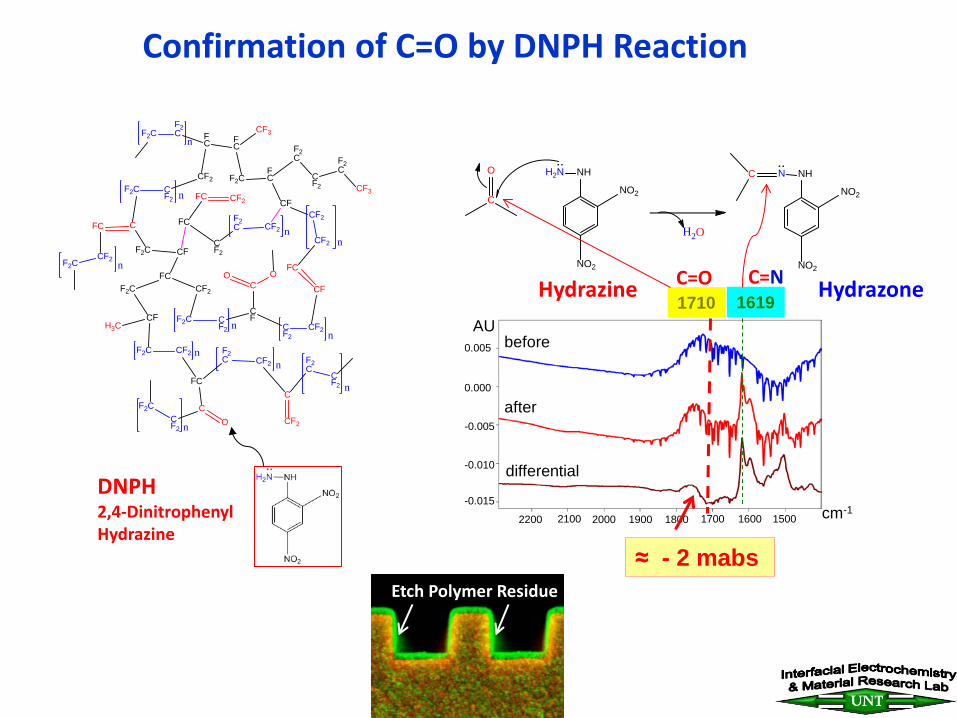
Confirmation of C=O by DNPH Reaction
DNPH 2,4-Dinitrophenyl Hydrazine
C=O C=N
≈ - 2 mabs Etch Polymer Residue
Hydrazine Hydrazone
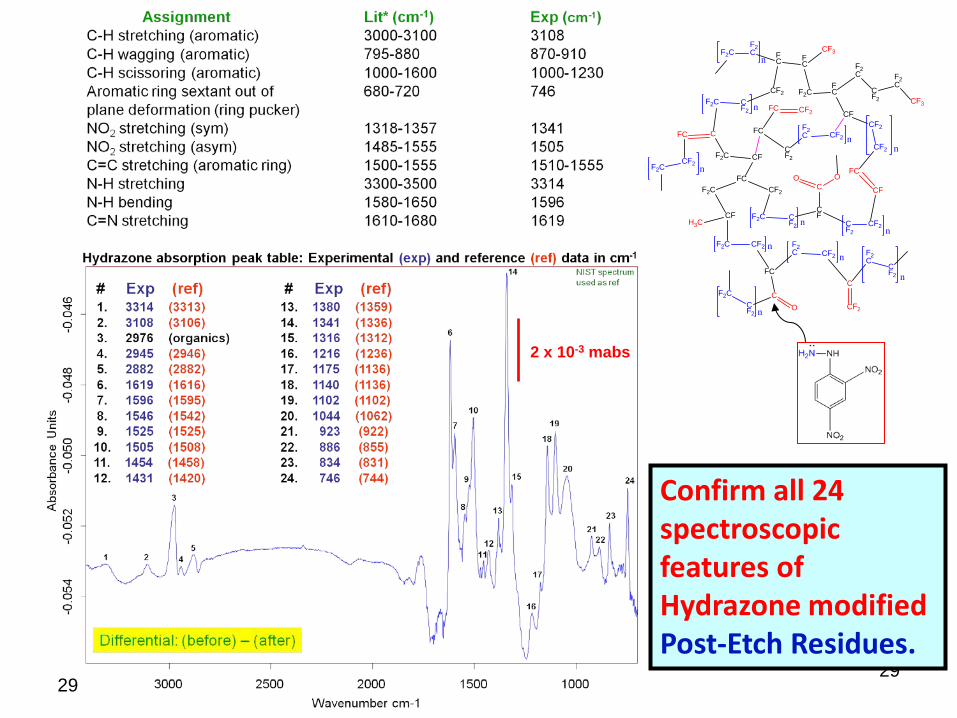
29
2 x 10⁻³ mabs
Confirm all 24 spectroscopic features of Hydrazone modified Post-Etch Residues.
29
FC
CF2
FC
CF
CF2CF2
CFC
F2F2C
CF2
FCF2C
CF
F2C CF2
FC
F2C CF2
CF
C
F2C
F2C
CCF2
O
H3C
C
F2C CF2 FC CF2
CF2
FC
CF2
CF2
F2C
n
n
CF2
FC F
C
F2CFC
F2C
F2C CF2
CFCF2
CF2
n
COO
n
n
n
n
nn
CF3F2C
CF2
F2C
CF3
F2C
n
F2Cn
1500 1000
4000 3500 2000 1500
0.60
0.70
0.90
0.80
3500 3000 2500 2000 1500 1000
FC
CF2
FC
CF
CF2CF2
CFC
F2F2C
CF2
FCF2C
CF
F2C CF2
FC
F2C CF2
CF
C
F2C
F2C
CCF2
O
H3C
C
F2C CF2 FC CF2
CF2
FC
CF2
CF2
F2C
n
n
CF2
FC F
C
F2CFC
F2C
F2C CF2
CFCF2
CF2
n
COO
n
n
n
n
nn
CF3F2C
CF2
F2C
CF3
F2C
n
F2Cn
C C
F
FBr
2C C
F
F
Br
C C
F
Br
Br
F
C C
F
Br
OH
F
H2O
Br
Br2
Before
After
Differential
After
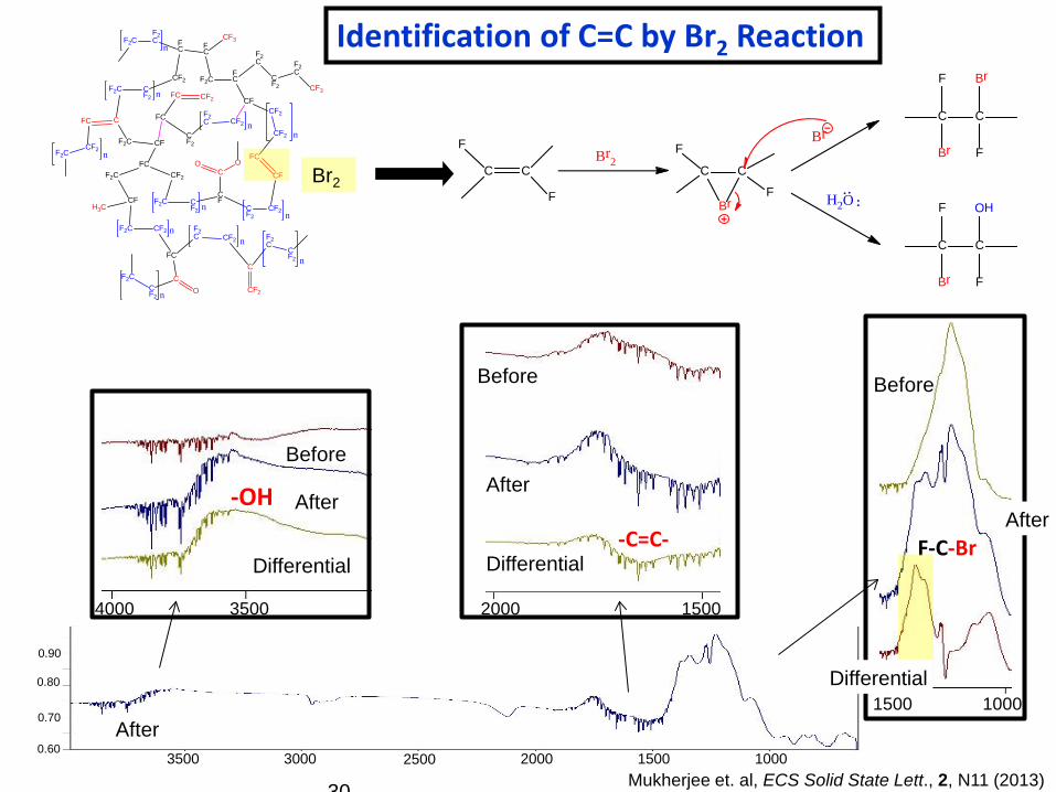
Identification of C=C by Br2 Reaction
-OH
Before
After
Differential -C=C- F-C-Br
Before
After
Differential
Mukherjee et. al, ECS Solid State Lett., 2, N11 (2013) 30
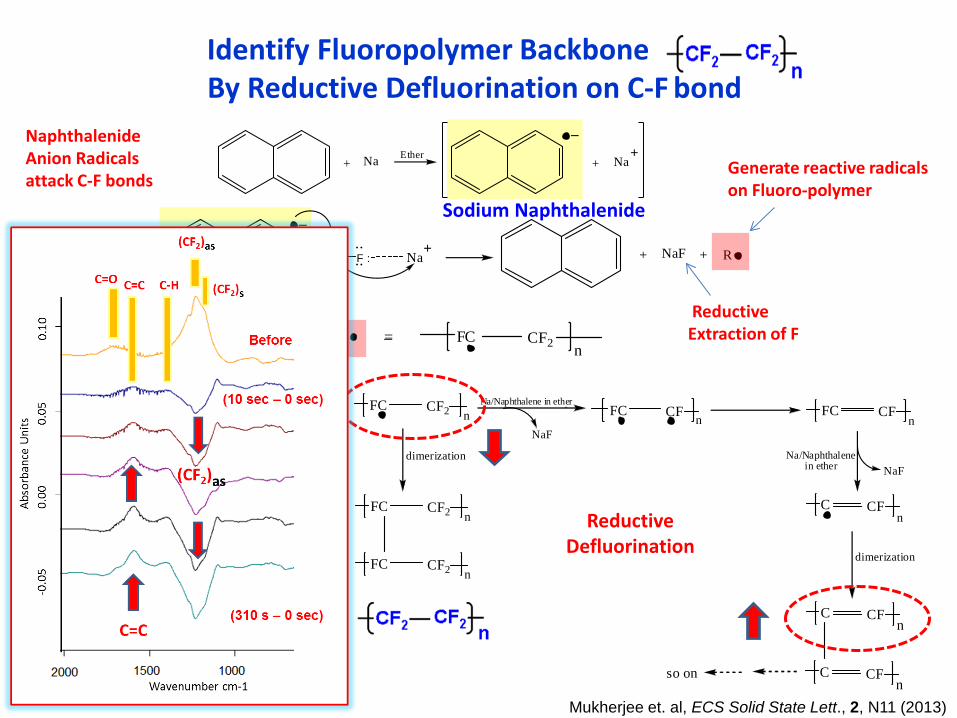
+ Na + NaEther
R F : Na + NaF + R
R FC CF2 n=_
Reductive Extraction of F
Naphthalenide Anion Radicals attack C-F bonds
FC CF2 n+
Na/Naphthalene in etherFC CF n
FC CFn
NaF
FC CF2 n
FC CF2 n
dimerization
C CFn
Na/Naphthalenein ether NaF
dimerization
C CFn
C CFn
so on
Generate reactive radicals on Fluoro-polymer
FC
CF2
FC
CF
CF2CF2
CFC
F2F2C
CF2
FCF2C
CF
F2C CF2
FC
F2C CF2
CF
C
F2C
F2C
CCF2
O
H3C
C
F2C CF2 FC CF2
CF2
FC
CF2
CF2
F2C
n
n
CF2
FC F
C
F2CFC
F2C
F2C CF2
CFCF2
CF2
n
COO
n
n
n
n
nn
CF3F2C
CF2
F2C
CF3
F2C
n
F2Cn
Reductive Defluorination
31
Sodium Naphthalenide
Identify Fluoropolymer Backbone By Reductive Defluorination on C-F bond
Mukherjee et. al, ECS Solid State Lett., 2, N11 (2013)
32
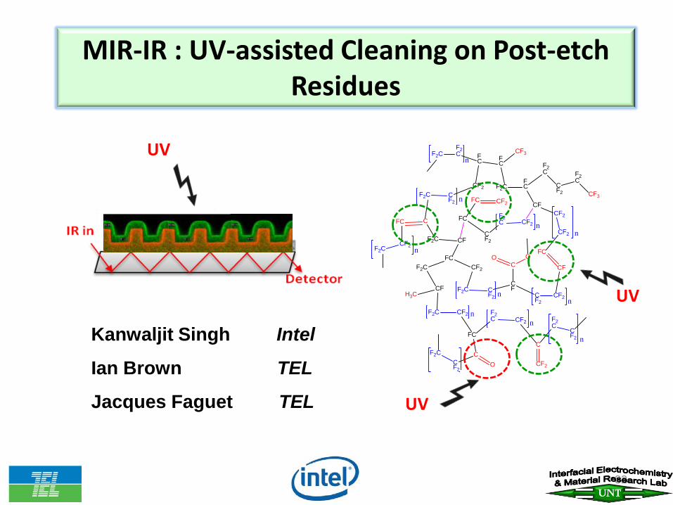
MIR-IR : UV-assisted Cleaning on Post-etch Residues
FC
CF2
FC
CF
CF2CF2
CFC
F2F2C
CF2
FCF2C
CF
F2C CF2
FC
F2C CF2
CF
C
F2C
F2C
CCF2
O
H3C
C
F2C CF2 FC CF2
CF2
FC
CF2
CF2
F2C
n
n
CF2
FC F
C
F2CFC
F2C
F2C CF2
CFCF2
CF2
n
COO
n
n
n
n
nn
CF3F2C
CF2
F2C
CF3
F2C
n
F2Cn
UV
UV
Kanwaljit Singh Intel
Ian Brown TEL
Jacques Faguet TEL
UV
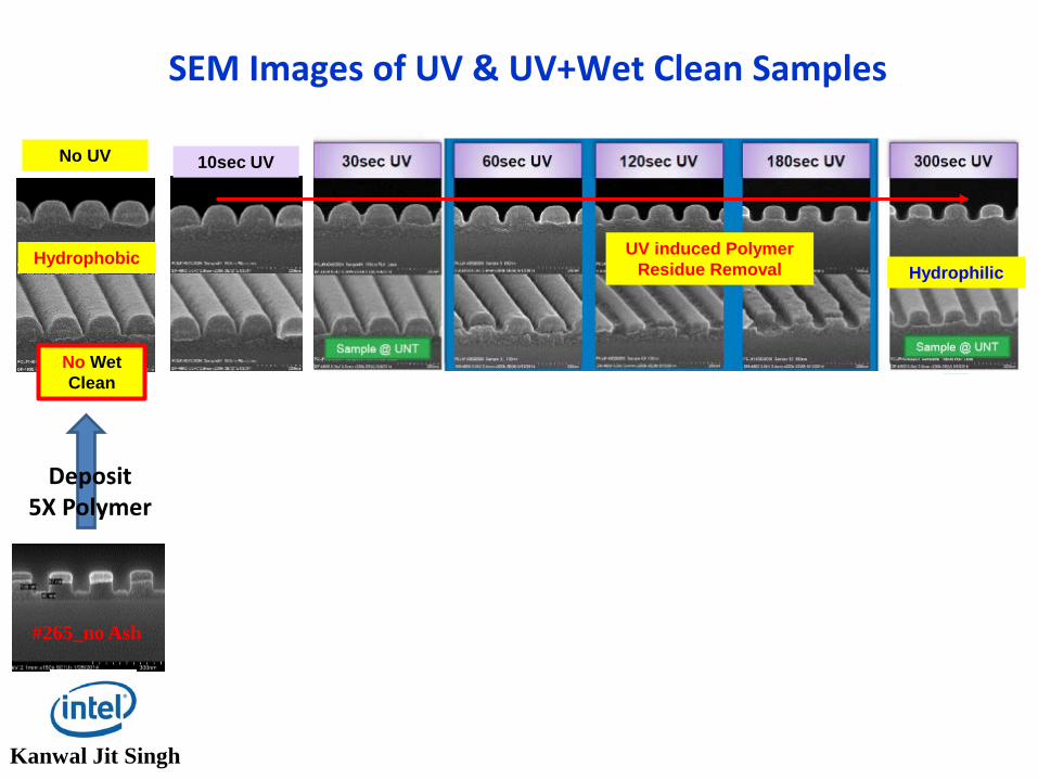
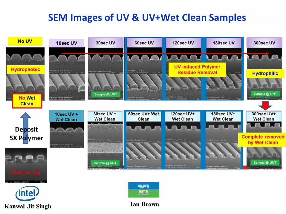
10sec UV
10sec UV + Wet Clean
No UV
Ian Brown
SEM Images of UV & UV+Wet Clean Samples
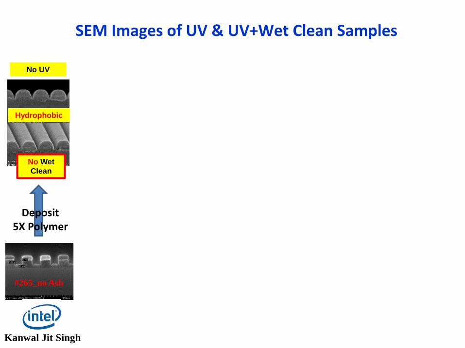
#265_no Ash
Deposit 5X Polymer
No Wet Clean
UV induced Polymer Residue Removal
Complete removed by Wet Clean
Hydrophobic Hydrophilic
Kanwal Jit Singh
10sec UV
10sec UV + Wet Clean
No UV
Ian Brown
SEM Images of UV & UV+Wet Clean Samples
#265_no Ash
Deposit 5X Polymer
No Wet Clean
UV induced Polymer Residue Removal
Complete removed by Wet Clean
Hydrophobic Hydrophilic
Kanwal Jit Singh
36
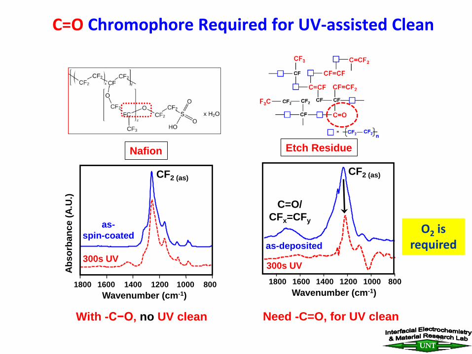
C=O Chromophore Required for UV-assisted Clean
800 1000 1200 1400 1600 1800 Wavenumber (cm-1)
as-deposited
300s UV
CF2 (as)
C=O/ CFx=CFy
800 1000 1200 1400 1600 1800
CF2 (as)
Nafion
as- spin-coated
300s UV
Abso
rban
ce (A
.U.)
Wavenumber (cm-1)
With -C−O, no UV clean Need -C=O, for UV clean
Etch Residue
O2 is required
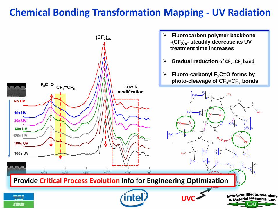
Fluorocarbon polymer backbone -(CF2)n- steadily decrease as UV treatment time increases Gradual reduction of CFx=CFx band
Fluoro-carbonyl FxC=O forms by
photo-cleavage of CFx=CFx bonds
Chemical Bonding Transformation Mapping - UV Radiation
FC
CF2
FC
CF
CF2CF2
CFC
F2F2C
CF2
FCF2C
CF
F2C CF2
FC
F2C CF2
CF
C
F2C
F2C
CCF2
O
H3C
C
F2C CF2 FC CF2
CF2
FC
CF2
CF2
F2C
n
n
CF2
FC F
C
F2CFC
F2C
F2C CF2
CFCF2
CF2
n
COO
n
n
n
n
nn
CF3F2C
CF2
F2C
CF3
F2C
n
F2Cn
UVC
CFx=CFx
Provide Critical Process Evolution Info for Engineering Optimization
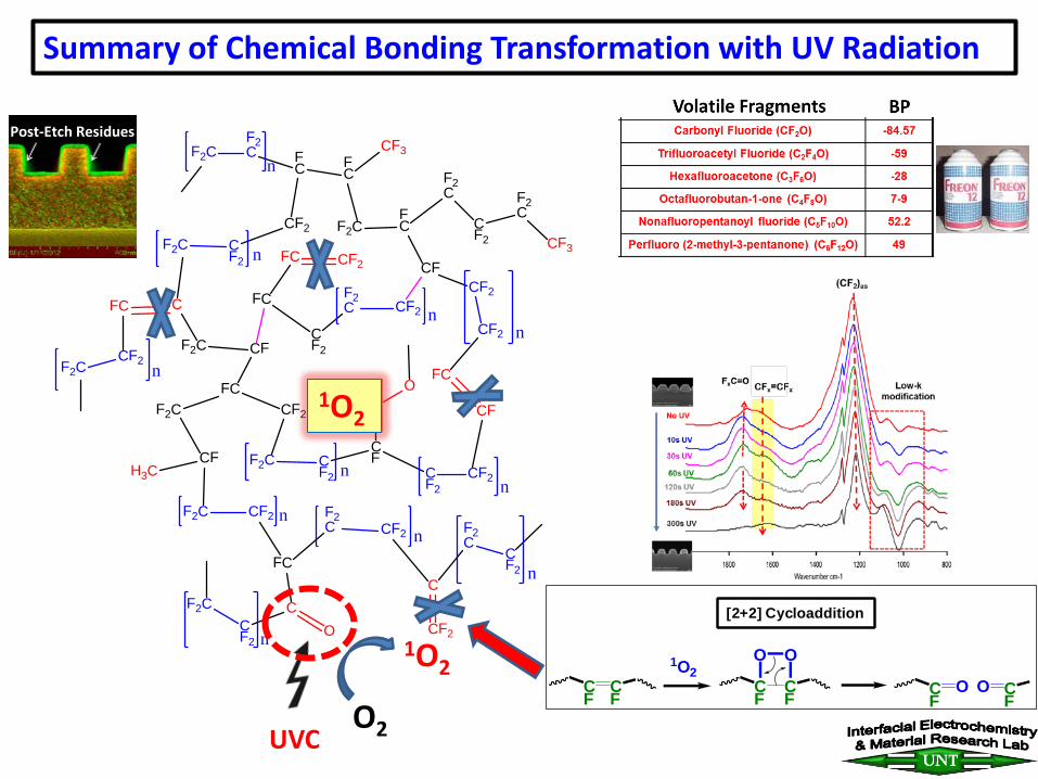
Summary of Chemical Bonding Transformation with UV Radiation
FC
CF2
FC
CF
CF2CF2
CFC
F2F2C
CF2
FCF2C
CF
F2C CF2
FC
F2C CF2
CF
C
F2C
F2C
CCF2
O
H3C
C
F2C CF2 FC CF2
CF2
FC
CF2
CF2
F2C
n
n
CF2
FC F
C
F2CFC
F2C
F2C CF2
CFCF2
CF2
n
COO
n
n
n
n
nn
CF3F2C
CF2
F2C
CF3
F2C
n
F2Cn
UVC
1O2
O2
1O2 1O2
[2+2] Cycloaddition
CF
CF
O O
CF
CF
O OCF
CF
Post-Etch Residues
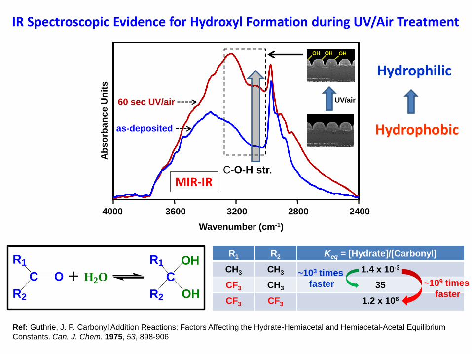
2400 2800 3200 3600 4000 Wavenumber (cm-1)
Abso
rban
ce U
nits
60 sec UV/air
C-O-H str.
OH OH OH
UV/air
C OR2
R1C
R2
R1 OH
OHH2O+
as-deposited
R1 R2 Keq = [Hydrate]/[Carbonyl]
CH3 CH3 1.4 x 10⁻³
CF3 CH3 35 CF3 CF3 1.2 x 10⁶
~103 times faster ~109 times
faster
Ref: Guthrie, J. P. Carbonyl Addition Reactions: Factors Affecting the Hydrate-Hemiacetal and Hemiacetal-Acetal Equilibrium Constants. Can. J. Chem. 1975, 53, 898-906
IR Spectroscopic Evidence for Hydroxyl Formation during UV/Air Treatment
Hydrophobic
Hydrophilic
MIR-IR
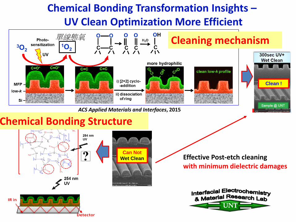
Chemical Bonding Transformation Insights – UV Clean Optimization More Efficient
Chemical Bonding Structure ACS Applied Materials and Interfaces, 2015
Effective Post-etch cleaning with minimum dielectric damages
Can Not Wet Clean
Clean !
單線態氧 Cleaning mechanism
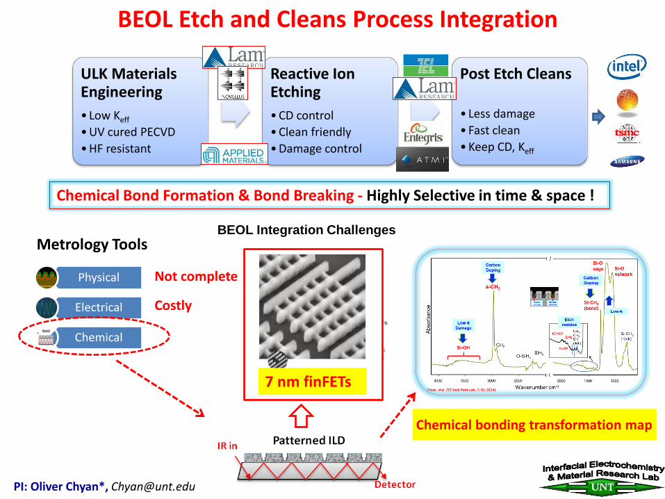
BEOL Integration Challenges
BEOL Etch and Cleans Process Integration
ULK Materials Engineering • Low Keff • UV cured PECVD • HF resistant
Reactive Ion Etching • CD control • Clean friendly • Damage control
Post Etch Cleans
• Less damage • Fast clean • Keep CD, Keff
Physical
Electrical
Chemical
Metrology Tools
Chemical Bond Formation & Bond Breaking - Highly Selective in time & space !
Chemical bonding transformation map
PI: Oliver Chyan*, [email protected]
Costly
Not complete
7 nm finFETs
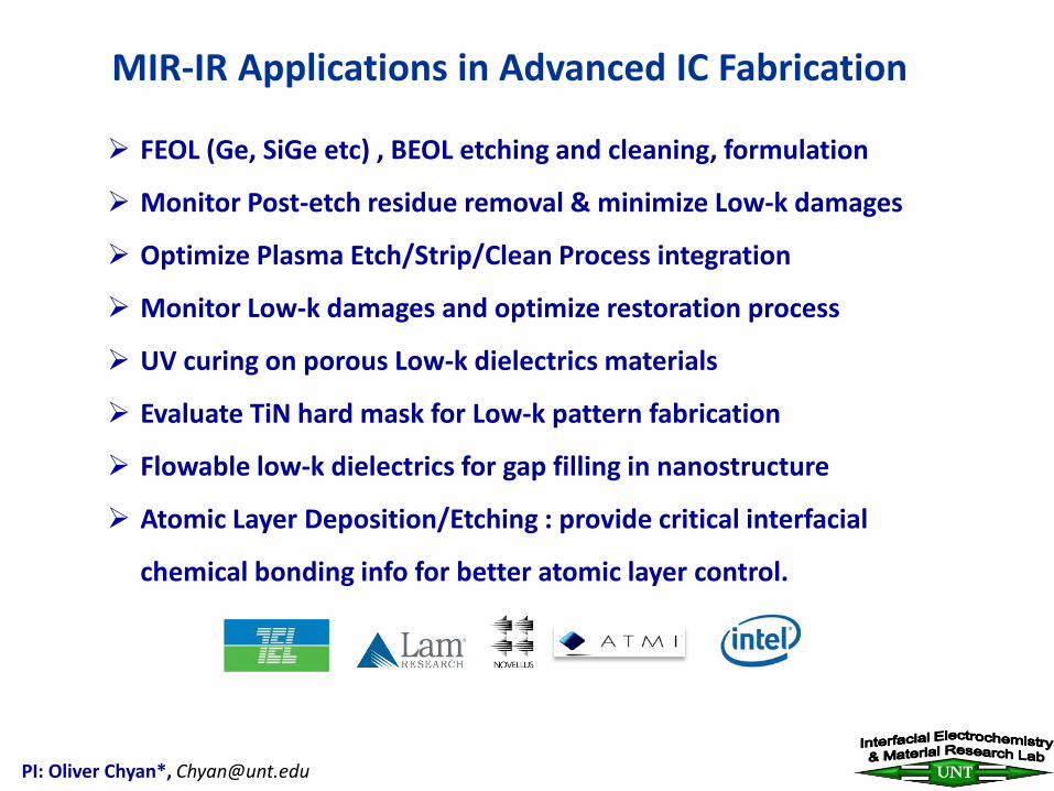
MIR-IR Applications in Advanced IC Fabrication
FEOL (Ge, SiGe etc) , BEOL etching and cleaning, formulation
Monitor Post-etch residue removal & minimize Low-k damages
Optimize Plasma Etch/Strip/Clean Process integration
Monitor Low-k damages and optimize restoration process
UV curing on porous Low-k dielectrics materials
Evaluate TiN hard mask for Low-k pattern fabrication
Flowable low-k dielectrics for gap filling in nanostructure
Atomic Layer Deposition/Etching : provide critical interfacial
chemical bonding info for better atomic layer control.
PI: Oliver Chyan*, [email protected]
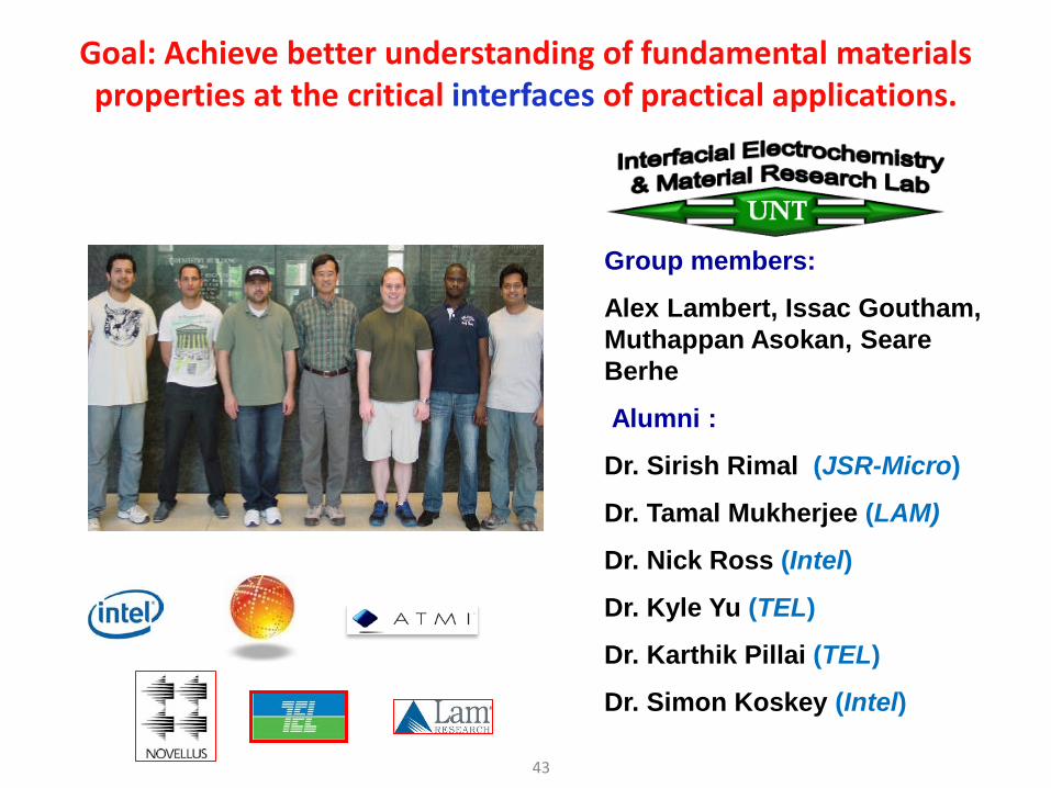
Goal: Achieve better understanding of fundamental materials properties at the critical interfaces of practical applications.
Group members:
Alex Lambert, Issac Goutham, Muthappan Asokan, Seare Berhe
Alumni :
Dr. Sirish Rimal (JSR-Micro)
Dr. Tamal Mukherjee (LAM)
Dr. Nick Ross (Intel)
Dr. Kyle Yu (TEL)
Dr. Karthik Pillai (TEL)
Dr. Simon Koskey (Intel)
43

END
44