Embed Size (px)
Citation preview

APPLIED PHYSICS REVIEWS
Chip-scale atomic devices
John KitchingTime and Frequency Division, National Institute of Standards and Technology, Boulder, Colorado 80305, USA
(Received 16 February 2018; accepted 1 May 2018; published online 14 August 2018)
Chip-scale atomic devices combine elements of precision atomic spectroscopy, silicon
micromachining, and advanced diode laser technology to create compact, low-power, and manufac-
turable instruments with high precision and stability. Microfabricated alkali vapor cells are at the
heart of most of these technologies, and the fabrication of these cells is discussed in detail. We
review the design, fabrication, and performance of chip-scale atomic clocks, magnetometers, and
gyroscopes and discuss many applications in which these novel instruments are being used. Finally,
we present prospects for future generations of miniaturized devices, such as photonically integrated
systems and manufacturable devices, which may enable embedded absolute measurement of a broad
range of physical quantities. VC 2018 Author(s). All article content, except where otherwise noted, islicensed under a Creative Commons Attribution (CC BY) license (http://creativecommons.org/licenses/by/4.0/). https://doi.org/10.1063/1.5026238
TABLE OF CONTENTS
I. INTRODUCTION . . . . . . . . . . . . . . . . . . . . . . . . . . . . 1
A. Atomic instrumentation: Clocks, sensors,
and fundamental constants. . . . . . . . . . . . . . . . 1
B. Alkali vapor cells . . . . . . . . . . . . . . . . . . . . . . . 3
C. Vapor cell atomic clocks . . . . . . . . . . . . . . . . . 5
D. Vapor cell atomic magnetometers . . . . . . . . . 7
E. Vapor cell NMR gyroscopes . . . . . . . . . . . . . . 8
F. Laser technology . . . . . . . . . . . . . . . . . . . . . . . . 9
II. MICROMACHINED ALKALI VAPOR CELLS . 10
A. Alkali metals . . . . . . . . . . . . . . . . . . . . . . . . . . . 10
B. Cell fabrication . . . . . . . . . . . . . . . . . . . . . . . . . 11
C. Introduction of alkali atoms. . . . . . . . . . . . . . . 12
D. Alternative cell geometries . . . . . . . . . . . . . . . 16
E. Alternatives to anodic bonding . . . . . . . . . . . . 17
III. MEMS-BASED ATOMIC CLOCKS. . . . . . . . . . . 18
A. Introduction . . . . . . . . . . . . . . . . . . . . . . . . . . . . 18
B. Design considerations . . . . . . . . . . . . . . . . . . . . 19
C. Physics packages . . . . . . . . . . . . . . . . . . . . . . . . 20
D. Compact, low-power local oscillators . . . . . . 22
E. Control electronics . . . . . . . . . . . . . . . . . . . . . . 23
F. CSAC prototypes . . . . . . . . . . . . . . . . . . . . . . . . 25
G. Performance and impact . . . . . . . . . . . . . . . . . 26
H. Applications . . . . . . . . . . . . . . . . . . . . . . . . . . . . 28
IV. CHIP-SCALE ATOMIC MAGNETOMETERS. . 29
A. Device design, fabrication, and performance 29
B. Chip-scale nuclear magnetic resonance . . . . . 31
C. Biomagnetics with chip-scale atomic
magnetometers . . . . . . . . . . . . . . . . . . . . . . . . . . 31
D. Chip-scale atomic magnetometers for space. 32
V. CHIP-SCALE ATOMIC GYROSCOPES. . . . . . . . 33
A. Nuclear magnetic resonance gyroscopes . . . . 33
B. Device design, fabrication, and performance 33
VI. OTHER INSTRUMENTS AND
TECHNOLOGIES. . . . . . . . . . . . . . . . . . . . . . . . . . . 34
A. Integration of atoms and photonics . . . . . . . . 34
B. Field imaging . . . . . . . . . . . . . . . . . . . . . . . . . . . 34
C. Other optical/atomic devices . . . . . . . . . . . . . . 35
VII. OUTLOOK. . . . . . . . . . . . . . . . . . . . . . . . . . . . . . . . 35
I. INTRODUCTION
A. Atomic instrumentation: Clocks, sensors, andfundamental constants
For the last half-century, atoms in the vapor phase or con-
fined in traps, where they interact only weakly with their envi-
ronment, have been a valuable tool for precision measurement.
Since measurements on these systems have been so successful,
in 1967, the second was redefined in terms of atomic energy
level structure to be the duration of 9 192 631 770 periods of
the radiation corresponding to the transition between the two
hyperfine-split levels of the ground state of the cesium atom.
Time remains the most accurately measured physical quantity
and frequency measurements usually result in the best mea-
surements of other physical quantities. For example, when the
speed of light was defined to be a fixed quantity in 1983, the
realization of the meter became fundamentally a measurement
of the frequency of optical radiation with respect to the SI
second.
There are several fundamental reasons why isolated
atomic systems are so useful in metrology. The first is that
isolated atoms are simple, well-defined quantum systems.
Every isolated atom of cesium or rubidium has identical
dynamics that depend only on fundamental (and presumably
invariant) constants of nature, a proposition articulated1 by
Sir William Thomson (later Lord Kelvin) in 1879. For
1931-9401/2018/5(3)/031302/38 VC Author(s) 2018.5, 031302-1
APPLIED PHYSICS REVIEWS 5, 031302 (2018)

example, the hyperfine Hamiltonian for the hydrogen atom is
given by
H ¼ 4
3
mec2a2gI
n31þ me
mp
� ��3~I � ~J ; (1)
where ~I and ~J are the (quantum mechanical) angular
momentum operators associated with the nucleus and elec-
tron, respectively; me and mp are the rest mass of the electron
and proton, respectively; c is the speed of light; a is the fine
structure constant; gI is the Lande g-factor of the proton; and
n is the energy quantum number. Under the assumption that
the atomic constants in Eq. (1) are not changing (and no vari-
ation has ever been observed), the energy level structure of
the hydrogen atom is also invariant in space and time and is
the same for every hydrogen atom. Transitions between other
energy levels in atoms (for example, Zeeman transitions or
optical transitions) have similar properties. It is such consid-
erations that have led to instruments based on atomic transi-
tions being referred to as “quantum technologies.”
Alkali atoms, with a single valence electron, are used in
almost all microwave atomic clocks for the following rea-
sons. First, they have a high vapor pressure at a given tem-
perature resulting in large spectroscopic signals. Second, the
non-zero nuclear spin leads to a ground state hyperfine split-
ting in the GHz range, which is a convenient frequency band
for standard RF electronics. Third, the simple electronic
structure allows for efficient optical pumping and the optical
absorption cross sections are large enough for efficient detec-
tion of the atomic state through interaction with an optical
field.
The energy spectrum of the 87Rb atom is shown in
Fig. 1. The S1/2 ground state is coupled to the two lowest
energy excited states, P1/2 and P3/2, by optical fields at 795
and 780 nm, respectively. These transitions, usually excited
by a lamp or a laser, allow efficient energy or spin optical
pumping2,3 by appropriately tuned and polarized optical
fields. They also provide a convenient, SI-traceable reference
for optical frequency and, ultimately, wavelength. Each of
these states has hyperfine structure with the energy splitting
in the MHz-GHz range. It is the ground state hyperfine split-
ting (6.8 GHz for 87Rb) that is used in most microwave
atomic clocks. Finally, each hyperfine level is split again in
the presence of a magnetic field. This Zeeman splitting or
Larmor frequency, which is on the order of 10 GHz/T, is
used in atomic magnetometers.
Because any interaction with the environment causes
environment-dependent deviations from this fundamental
dynamics, much of the work in the area of atomic clocks, for
example, is focused on this one goal: isolating atoms from
their environment. Under this condition, the dynamics of
atomic systems can have very long relaxation times and cor-
responding high quality factors (Q). Optical coherences in
trapped ions, for example, have reached Q’s well above4
1015. This remarkable property of atomic systems has
resulted in optical atomic clocks that now reach frequency
uncertainties in the low 10�18 range.5 In the microwave
domain, hyperfine coherences in alkali atoms can have relax-
ation times near 100 ms in alkali cells containing buffer
gases6,7 and near 1 s in atomic fountains based on laser-
cooled atoms.8,9 Spin coherence times in atoms confined in
buffer gases are typically near 1 s for cells on the size scale
of 10 cm, and even longer spin coherence times have been
reported in wall-coated cells.10 Finally, nuclear spin coher-
ence times of atoms in the vapor phase can be as high as sev-
eral days.11,12
The commercial atomic clock market today is domi-
nated by two clock designs: vapor cell atomic clocks, dis-
cussed in detail below and usually based on Rb, and beam
clocks based on Cs. Vapor cell clocks rely on an atomic
vapor coexisting with a solid or liquid phase, all confined in
a cell. They are smaller and less expensive than beam clocks
and are typically used where timing over hours to days is
important. The largest application space for vapor cell clocks
at present is base stations for cellular telephone systems.
Beam clocks, based on a collimated beam of atoms moving
at thermal velocities along a single axis, are larger and more
expensive and tend to be used in applications where accuracy
or stability over periods longer than one month are impor-
tant. Beam clocks are used as master clocks for high-speed
telecommunications systems and for basic time and fre-
quency metrology.
More advanced atomic clocks are under development in
laboratories around the world, but significant use as com-
mercial products is not yet found. Fountain clocks use laser-
cooled atoms to lengthen the time in which the atoms can
oscillate without perturbation and currently serve as the best
realizations of the SI second13,14 at a level of about 10�16.
FIG. 1. Energy level spectrum of 87Rb.
031302-2 John Kitching Appl. Phys. Rev. 5, 031302 (2018)

Optical clocks5 are based on laser-interrogation of optical
transitions in atoms. They have emerged over the last two
decades as the highest-performing timing instruments due to
the development of optical frequency combs, which can effi-
ciently divide the high optical frequency down to the micro-
wave domain where the signal can be counted and used for
timing. Currently, clocks based on single trapped ions and
those based on neutral atoms trapped in an optical lattice
both achieve frequency uncertainties below 10�17.
Chip-scale atomic clocks (CSACs) grew out of a con-
vergence of atomic spectroscopy, silicon micromachining,
and semiconductor laser technology in the early 2000s.
These atomic clocks combine small size and low power with
moderate frequency stability in the 1 h to 1 week time frame.
A significant research effort was undertaken in the United
States by multiple teams throughout the 2000s, culminating
in the release of a commercial product in 2011. The work on
chip-scale atomic clocks and related instruments continues
to this day at a rapid pace, with active programs in countries
throughout the world including France, Switzerland,
Germany, The United Kingdom, Japan, and China.
In this section, we introduce the basic physics and instru-
mentation concepts that underlie chip-scale atomic devices. In
most cases, this physics is several decades old and is reviewed
here to enable a clearer understanding of subsequent sections
of the paper. In Sec. II the fabrication of micromachined
alkali vapor cells, first developed in the early 2000s, is dis-
cussed. The use of these microfabricated cells in clocks, mag-
netometers, and gyros is discussed in Secs. III–V, and the
emerging applications in which these unique instruments are
being used are identified in Sec. VI. Section VII concludes
with a discussion of more recent, forward-looking work that
may hint at what the future holds for chip-scale atomic
devices.
B. Alkali vapor cells
Evacuated glass cells containing alkali atoms have been
used in atomic spectroscopy as far back as the 1950s. The
cells are typically made using glassblowing techniques, in
which a sealed glass container is fitted with a filling tube
through which the cell is evacuated before a small quantity
of solid or liquid alkali metal is distilled into the cell body.
The filling tube is then sealed by heating. Without any addi-
tional gas added to the cell, the alkali atoms undergo ballistic
transport across the vapor cell, at velocities of a few hundred
m/s and with a typical transit time on the order of 1 ls for a
cell of 1 cm in size. Since collisions with untreated glass cell
walls completely depolarize the spin of the atoms, the
Fourier limited “transit time” width of any atomic coherence
is near 1 MHz and the resulting quality factor for a hyperfine
resonance is about 104. Doppler broadening of the transition
is also present and limits the Q to about 106.
The addition of inert “buffer” gases to the cell can sub-
stantially narrow the transition linewidths. Gases such as Ne,
N2, Ar, and He interact only very weakly with the spin of the
alkali atoms and hence the atoms can undergo many colli-
sions (typically hundreds of thousands) with the buffer gas
before the spin depolarizes. The result is that for typical
buffer gas pressures of �10 Torr, the mean free path of the
alkali atoms is on the order of 1 lm and the atoms undergo
diffusive motion through the cell rather than ballistic motion.
The time between depolarizing wall collisions is therefore
considerably longer, typically �10 ms for a 1 cm cell with
10 Torr of buffer gas. In addition, the short mean-free-path
leads to “Dicke narrowing,”15 in which Doppler broadening
from the atoms’ thermal motion is suppressed.
The buffer gas is not completely benign, however. Some
small relaxation of the hyperfine or Zeeman transitions does
occur due to collisions and for hyperfine transitions, the tran-
sition line is significantly shifted16 and broadened. Typically,
the buffer gas pressure is adjusted to balance relaxation from
the walls, which is inversely proportional to the buffer gas
pressure P, and relaxation from buffer gas collisions, which
is proportional to P. The relaxation rate for a diffusion mode
� is then given by3
C� ¼ c0
P
760 Torr
� �þ D0
K2�
760 Torr
P
� �; (2)
where c0 and D0 are the relaxation rate and diffusion con-
stant of the alkali atoms at 760 Torr, and K� is the diffusion
length for the mode �. Usually only the lowest-order diffu-
sion mode is considered (the others decay more rapidly), for
which K0 � L, where L is the length of the cell. For example,
for a cylindrical cell of radius a and length L, the diffusion
length of the lowest-order mode is given by17
1
K20
¼ 2:405ð Þ2
a2þ p2
L2
" #: (3)
The coefficients c0 and D0 have been measured for many
combinations of buffer gases and alkali atoms and are tabu-
lated in various places.3,17 From Eq. (2), the relaxation rate
of the lowest-order diffusion mode as a function of buffer
gas pressure exhibits a broad minimum near a pressure of
Popt ¼ffiffiffiffiffiffiD0
c0
s1
K0
760 Torrð Þ; (4)
for which the relaxation rate is C0 ¼ 2
ffiffiffiffiffiffiffic0D0
pK0
and the broad-
ening of the transition linewidth is therefore
D�bg ¼2
p
ffiffiffiffiffiffiffiffiffiffic0D0
p
K0
: (5)
Spin-exchange collisions between alkali atoms can also
cause broadening proportional to the alkali atom density. For
Rb, for example, spin-exchange collisions result in a broad-
ening of the hyperfine transition linewidth of about 700 Hz
at a cell temperature of 85 �C. Spin exchange broadening
becomes increasingly important for small cell sizes where
higher alkali densities are needed to give optimal signals.
Spin-exchange relaxation is also important for atomic mag-
netometers, which typically operate at higher cell tempera-
tures than atomic clocks.
For optimal buffer gas pressure, the relaxation rate is
therefore inversely proportional to the cell size. Typical
031302-3 John Kitching Appl. Phys. Rev. 5, 031302 (2018)

relaxation rates (and optimal buffer gas pressures) for hyper-
fine transitions are a few hundred s�1 (a few tens of Torr) for
cm-scale cells and a few thousand s�1 (a few hundreds of
Torr) for mm-scale cells. Since the collisions between alkali
atoms and the buffer gas are electronic in nature, the pres-
ence of the buffer gas results in significant homogeneous
broadening of the optical transitions, typically by �20 MHz/
Torr.17 At 500 Torr, this broadening is �10 GHz, implying
that both the ground state and excited state hyperfine struc-
tures are unresolved. This imposes some limitations on the
types of spectroscopy that can be carried out. For example,
optically excited higher-order coherences usually require
resolved excited state hyperfine structure.
Molecular nitrogen has a unique role in vapor cells
because of its very large excited state quenching cross-
section for alkali atoms. In the presence of N2, alkali atoms
decay non-radiatively from their excited states via transfer of
energy to ro-vibrational modes of the molecule, and the
issues related to radiation trapping can be avoided.
Collisions of the alkali atoms with the buffer gas also
result in a net shift of the hyperfine frequency. During such a
collision, the alkali atoms spend a short time in the potential of
a buffer gas atom, during which the energy levels of the alkali
atom are shifted from their unperturbed values. Averaged over
many collisions, this results in a net shift that depends on the
buffer gas density and the cell temperature.16,18 This shift can
be written (to second order in temperature) as17
�bg ¼ P0 b0 þ c0 T � T0ð Þ þ d0 T � T0ð Þ2� �
; (6)
where P0 is the buffer gas pressure; T is the cell temperature;
and b0, c0, d0; and T0 are phenomenological constants spe-
cific to a given buffer gas and alkali atom species.19 The val-
ues of b0 and c0 depend on the alkali species and buffer gas
but are (fractionally) on the order of17 10�7/Torr and 10�11/
Torr/K, respectively, which can lead to significant clock
instabilities if the temperature of the vapor cell fluctuates.
Lighter buffer gases result in temperature coefficients c0 of
opposite sign from those of heavier buffer gases. It is there-
fore possible to use combinations of buffer gases to bring the
first-order dependence of the buffer gas shift to zero at some
specific temperature, resulting in a residual second-order
shift.6 When the vapor cell is stabilized at this temperature,
the sensitivity of the hyperfine frequency to temperature var-
iations is reduced dramatically and the stability of a clock is
improved correspondingly.
An alternative approach to reduce the effects of wall colli-
sions is to apply a coating such as paraffin on the interior walls
of the vapor cell.20,21 While similar (and sometimes even nar-
rower) linewidths can be obtained, wall coatings have not gen-
erally been adopted for vapor cell atomic clocks, in part due to
the instability of the coating materials at elevated temperatures.
However, wall coatings offer some significant advantages for
chip-scale atomic clocks and magnetometers, since the excited
state hyperfine structure can be well resolved while still achiev-
ing narrow Zeeman and hyperfine transitions.
When an alkali atom collides with, for example, a paraffin-
coated wall, the energies of the hyperfine-split ground states of
the atom are shifted relative to each other by the Van der Walls
interaction. This energy splitting, averaged over the time the
atom spends on the wall (the adsorption time), results in a phase
shift, /, of the atom’s hyperfine coherence. Under the assump-
tion that /� 1, the cumulative effect of many such collisions
is an overall shift in the hyperfine frequency by
�w ¼/
2ptc; (7)
where / is the average phase shift per collision and tc is the
average time between collisions. The parameter /; therefore,
represents a property of the coating, which is independent of
size and shape of the vapor cell, and is the primary way in
which a particular wall coating is characterized.
Wall collisions also result in line broadening, primarily
because of the dispersion in adsorption time, which causes a
dispersion in /. Under some conditions,21 it can be shown that
after N collisions, the dispersion in the accumulated phase shift
is d/ tð Þ ¼ffiffiffiffiNp
/ ¼ffiffiffittc
q/; and the resonance width is22
D�w ¼/
2
ptc: (8)
For example, the average phase shift for the hyperfine transition
of 87Rb on ParaflintTM is23 �0.08 rad, from which the wall shift
and relaxation linewidth can be calculated from the above
equations.
The interaction of an atom with a wall coating can also
be characterized by the average number of wall bounces, Nb,
which an alkali atom can undergo before it relaxes. This is
given by the condition21
1
2Nb/
2 ¼ 1; (9)
which leads to an alternate formulation of the linewidth as
D�w ¼2
pNbtc: (10)
The linewidths for a cell with diameter equal to length
are shown as a function of buffer gas pressure and cell diam-
eter in Fig. 2. As a function of buffer gas pressure, the line-
width exhibits a broad minimum at the pressure for which
the relaxation due to wall collisions is equal to the relaxation
due to buffer gas collisions, as shown in Fig. 2(a). An opti-
mal buffer gas pressure and corresponding linewidth exist
for each cell diameter, as predicted by Eqs. (4) and (5). For a
wall-coated cell, the linewidth decreases inversely with the
cell diameter, as indicated by Eq. (7). For buffer gas cells at
a fixed buffer gas pressure, the linewidth is a constant at
large cell diameter, where the linewidth is dominated by
buffer gas collisions, and increases at smaller cell sizes
where the effects of wall relaxation dominate, as shown in
Fig. 2(b). The “knee” in these curves represents the optimal
linewidth and corresponding minimum cell diameter for the
given buffer gas pressure. These optimal linewidths decrease
inversely with the cell diameter as indicated by Eq. (5).
031302-4 John Kitching Appl. Phys. Rev. 5, 031302 (2018)

The light used for optically pumping and probing the
atoms also results in a shift of the atomic energy levels. For
a near-resonant optical field interacting with a two-level
atom, the scalar AC Stark shift is
�LS ¼1
4
X2D
D2 þ C=2pð Þ2; (11)
where X is the Rabi frequency, D is the detuning from opti-
cal resonance, and C is the relaxation rate of the excited
state. Since the intensity I � X2, this shift is proportional to
the intensity of the interrogating light. For a two-level sys-
tem, this light shift is zero when the optical field is exactly
on resonance with the atomic transitions. In real atoms, how-
ever, the optical field interacts with transitions to many other
atomic energy levels, resulting in an overall light shift even
in perfect resonance with a single transition.
For polarized atoms interacting with a polarized optical
field, a second-order AC Stark effect can shift the Zeeman-
split levels. For circularly polarized light and a homoge-
neously broadened transition, this shift can be viewed as a
fictitious magnetic field proportional to the light intensity
and directed along the k-vector of the optical field24,25
BLS ¼ �recfU
cD
D2 þ C=2pð Þ2; (12)
where re is the classical electron radius, c is the speed of
light, f is the transition strength, U is the photon flux, and cis the gyromagnetic ratio of the electron.
Microwave atomic clocks typically use the first-order
magnetically insensitive transition between the mF ¼ 0 lev-
els of the hyperfine ground states. This transition has a
second-order magnetic field shift
�Z;2 ¼gJ þ gIð Þ lBð Þ=�h
� �2�hfs
B20; (13)
which can be important for very high performance or accu-
rate atomic clocks.
C. Vapor cell atomic clocks
Vapor cell atomic clocks6,26–28 are based on the excita-
tion of hyperfine transitions in alkali atoms (usually 87Rb)
confined in a vapor cell; a typical configuration is shown in
Fig. 3. In this implementation, an RF 87Rb discharge lamp
produces pump light resonant with optical transitions in 87Rb.85Rb has an absorption resonance nearly overlapping one, but
not both, of the spectral lines emitted by the lamp; a cell con-
taining 85Rb positioned between the lamp and the reference
cell filters the light and creates an intensity imbalance
between the spectral lines emitted by the lamp. This imbal-
anced spectrum optically pumps 87Rb atoms in the reference
cell into the F¼ 2 hyperfine ground state, which results in an
increased transmission of the pump light through the cell.
The reference cell, also containing a suitable buffer gas
to reduce the hyperfine transition linewidth, is situated inside
a microwave cavity tuned to the hyperfine resonance fre-
quency. Microwaves applied to the cavity induce transitions
between the hyperfine states in the 87Rb atoms only when
the microwave frequency corresponds to the atomic hyper-
fine transition frequency. Under this resonance condition, the
population difference between the two hyperfine states is
driven toward zero and the pump absorption increases
toward its equilibrium value. By monitoring the transmitted
pump power on a photodiode, the reference oscillator that
serves as the microwave source can be locked electronically
onto the atomic transition and stabilized. The entire device is
placed inside a magnetic shield to prevent magnetic-field
FIG. 2. (a) Hyperfine linewidth for a cylindrical cell with its diameter equal to
its length, L, as a function of buffer gas pressure for 85Rb in N2 at 85 �C and
L¼ 1 mm. The dashed lines show the contributions due to wall relaxation (red),
Rb-Rb spin-exchange collisions (blue), and Rb-buffer gas collisions (magenta).
The green solid line shows the total linewidth, with a broad minimum near
300 Torr as a function of cell diameter. (b) Hyperfine linewidth as a function of
cell diameter. The solid lines assume a N2 buffer gas pressure of 100 Torr (black),
300 Torr (red), and 1000 Torr (blue). The magenta dashed line indicates the line-
width of a cell with no buffer gas and a wall coating with NB ¼ 1000. The black
dotted-dashed line indicates the spin-exchange relaxation linewidth at T¼ 85 �C.
Note: calculated linewidths are approximate as relaxation cross-sections are not
known exactly.
031302-5 John Kitching Appl. Phys. Rev. 5, 031302 (2018)

induced changes in the atomic energy spectrum and hence
the frequency of the clock.
With the advent of semiconductor lasers able to be tuned
to the relevant transitions in alkali atoms, new approaches to
vapor cell atomic clocks have been possible. In one such
approach, optically induced hyperfine coherences based on
the phenomenon of coherent population trapping (CPT)29,30
are used, as shown in Fig. 4. Instead of applying the micro-
wave field directly to the atoms, the injection current of a
diode laser is instead modulated, which creates sidebands on
the optical carrier spaced by the hyperfine frequency (or a
sub-harmonic). When the modulation frequency is equal to
the ground state hyperfine splitting, the resulting optical
spectrum optically pumps the atoms into a coherent dark
state: a superposition state of the two hyperfine ground states
that does not absorb the pump light. The power transmitted
through the reference cell therefore increases, leading to a
detectable CPT resonance, which is used to stabilize the ref-
erence oscillator as above. In a longitudinal magnetic field,
linearly polarized light does not excite CPT resonances
between magnetically insensitive levels for symmetry rea-
sons, and a quarter-wave plate is needed in the beam path to
convert the light from the linearly polarized output of the
laser to circular polarization.
CPT excitation has the advantage over conventional
microwave excitation that a microwave cavity is not required
around the atoms. This leads to a reduced experimental com-
plexity and the possibility of smaller size, since the conven-
tional microwave cavities used in most vapor cell atomic
clocks must be larger than one-half the wavelength of the
microwave radiation (2.2 cm for 87Rb) to be resonant.
Coherent population trapping was investigated31–35 in the
context of atomic beam clocks throughout the 1980s. More
recently, CPT has been used in vapor cell clocks,36,37 includ-
ing CPT masers.38–41 Most chip-scale atomic clocks rely on
coherent population trapping, although new miniature micro-
wave cavities42 remain a viable alternative for miniaturized
atomic clocks. A review of the application of CPT to atomic
clocks can be found in Ref. 43.
The use of a laser also relaxes the need to use Rb as the
reference atom. Traditionally, Cs has not been used in vapor
cell atomic clocks because there is no good way of spectrally
filtering the light generated by the lamp to achieve hyperfine
optical pumping. Because a single-mode laser lases at one
wavelength only, hyperfine optical pumping can also be
achieved in Cs (or even K).
A modulation of the current of a diode laser produces a
combination of AM and FM modulation on the optical field
because of the linewidth enhancement factor44 present in the
semiconductor gain media. When the buffer gas pressure in
the cell is small enough that optical transitions from the
hyperfine ground states to the excited state are well resolved,
both AM and FM modulation produce the same CPT signal.
For higher buffer-gas pressures, however, when the transi-
tions overlap, it has been demonstrated45 that AM modula-
tion produces a strong CPT signal, while the destructive
interference that occurs for FM modulation results in a
strongly suppressed CPT signal.
Discharge lamps typically operate on 1 W of power or
more, and the use of a laser can considerably reduce the
power needed to produce the light. As discussed below,
vertical-cavity surface emitting lasers are a suitable light
source for CPT atomic clocks and can operate on only a few
mW of power. Microfabricated46,47 discharge lamps with
potentially lower power than their larger counterparts are
FIG. 3. (a) Vapor cell atomic clock. (b) The clock operation can be thought
of as occurring in in three steps: optical pumping to prepare the atomic state;
coherent, resonant microwave excitation; and optical detection of the final
state. Feedback of the detected signal to the drive oscillator stabilizes its fre-
quency to the atomic transition. In practice, all steps occur simultaneously.
FIG. 4. Vapor cell atomic clock based on coherent population trapping. A
modulated laser excites hyperfine coherences without any direct application
of microwaves to the atomic ensemble.
031302-6 John Kitching Appl. Phys. Rev. 5, 031302 (2018)

currently under development and may provide an alternative
to low-power lasers for future chip-scale atomic devices.
Current commercial compact vapor cell atomic clocks
have volumes of about 0.1 l, consume about 10 W of electri-
cal power, and achieve short-term fractional frequency sta-
bilities of around 10�11 at 1 s of integration. The long-term
drift is about 10�11/month. The main commercial application
for this type of clock is in synchronization of telecommuni-
cations systems such as cell phone networks.48 Research
instruments being developed for next-generation satellite
navigation systems achieve about two orders of magnitude
better short- and long-term stability in the laboratory.49
D. Vapor cell atomic magnetometers
Atomic (or optical) magnetometers50 have an overall
design, shown in Fig. 5, very similar to that of a vapor cell
atomic clock. Once again, there is a discharge lamp (or laser)
as the light source and a reference cell containing the alkali
atoms. Magnetometers, however, rely on the Zeeman split-
ting of the atomic energy levels rather than the hyperfine
splitting (see Fig. 1). The optical pumping is with respect to
the spin degree of freedom rather than the energy degree of
freedom. The pump light must therefore be polarized, but
does not need to be spectrally filtered. In a spin precession
magnetometer, a precession of the atomic spins about the
ambient magnetic field can be driven by a pair of Helmholtz
coils and defines a Larmor frequency from which the field
can be determined. Once again, a photodiode detects the
response of the atomic system to the applied RF field, and
the resulting signal is used to stabilize the drive oscillator
onto the Larmor frequency.
Both the AC (Mx mode) and DC (Mz mode) signals
from the photodiode can be used.51 In the Mx mode, the
phase of the photodiode signal at the drive frequency is com-
pared with the phase of the drive frequency itself, and a dis-
persive error signal is generated as this frequency is scanned
across the magnetic resonance line. In the Mz mode, the DC
photodiode signal is used to measure the magnitude of the
projection of the spin precession onto the magnetic field
axis. This signal is symmetrical about the magnetic reso-
nance and is converted to a dispersive signal using a modula-
tion of the drive frequency and lock-in detection. The Mx
mode has better sensitivity and bandwidth, while the Mz
mode is less sensitive to the sensor’s orientation in the mag-
netic field (has lower heading error). Since the spin preces-
sion frequency depends only on the magnitude of the
ambient magnetic field, these sensors are referred to as scalar
sensors and are useful on moving platforms since the chang-
ing projection of the ambient magnetic field onto the sensor
axis does not change the sensor reading.
At very low magnetic fields (such that the Larmor fre-
quency is much smaller than the relaxation rate of the
atoms), an alternative “zero-field” approach52 can be used.
Here, there is no drive field at the Larmor frequency, and
instead the presence of a weak magnetic field perpendicular
to the atomic polarization induces a quasi-static reorientation
of the atomic spin polarization. This reorientation results in
increased optical absorption, and hence a zero-field reso-
nance in the transmission spectrum of the light as a function
of magnetic field. By applying a low-frequency transverse
field and using lock-in detection, this absorptive resonance
can be turned into a dispersive resonance with a maximal
slope at zero field suitable for detection. Zero field magneto-
meters operated at high atomic densities (i.e., high cell tem-
peratures) exhibit a remarkable suppression of spin-
exchange collisions53,54 that can lead to strong, narrow zero
field resonances. Such resonances have been used in spin-
exchange relaxation-free (SERF) magnetometry to achieve
exceptionally high field sensitivities, below 1 fT/�Hz.55,56 It
was recognized early on53 that SERF magnetometry would
be particularly important for highly miniaturized sensors
where high alkali atom densities are required to offset the
shorter optical path length.
Light narrowing57 can also be used to reduce broadening
due to spin-exchange collisions and improve the sensitivity
of atomic magnetometers. Light narrowing is the use of
strong optical fields to optically pump most of the atoms into
the same high-angular momentum state resulting in reduced
angular momentum transfer between colliding atoms. This
line-narrowing method is not as effective as the full suppres-
sion of spin-exchange broadening achieved at high alkali
densities and low magnetic fields, but has the advantage that
it can operate in high fields.
Current commercial atomic magnetometers have vol-
umes of about 1 l, consume about 10 W of power while oper-
ating, and achieve a field sensitivity of 1 pT at 1 s of
integration time. The main applications are oil and mineral
FIG. 5. (a) Atomic (or optical) magnetometer. (b) A circularly polarized
light beam spin-polarizes the atomic ensemble; RF coils drive a precession
of the spins about the ambient magnetic field; final orientation of spins is
detected optically. Measurement of the resulting Larmor frequency is used
to determine the ambient magnetic field.
031302-7 John Kitching Appl. Phys. Rev. 5, 031302 (2018)

exploration, the detection of unexploded ordinance, and
magnetic anomaly detection.
E. Vapor cell NMR gyroscopes
Vapor cell nuclear magnetic resonance (NMR) gyro-
scopes58–60 are also based on the precession of atomic spins
in a magnetic field. If such a field is kept very stable, a rota-
tion of the apparatus about the field axis results in change in
phase of the atomic spins with respect to the apparatus coor-
dinate system. This phase shift can be measured and the rota-
tion rate can be deduced from the apparent shift of the spin
precession frequency. Although electron spins in alkali
atoms can, in principle, be used, nuclear spins in noble gases
have considerably longer spin relaxation times, are less sen-
sitive to magnetic fields, and result in better gyro perfor-
mance. The basic design of an NMR gyro is shown in Fig. 6.
As in an atomic magnetometer, alkali spins in a vapor cell
are optically pumped with a circularly polarized pump beam.
A noble gas with non-zero nuclear spin is confined inside the
cell with the alkali atoms and becomes polarized itself
through spin-exchange collisions with the alkali atoms.61
A transverse coil creates an oscillating magnetic field at the
approximate Larmor frequency of the noble gas which drives
a precession of the nuclear spins about a static applied mag-
netic field. These precessing spins have a magnetization,
which adds transversely to the static magnetic field seen by
the alkali atoms. The alkali atoms therefore see a magnetic
field precessing at the nuclear Larmor frequency on a cone
whose axis is defined by the original static field. A pair of
longitudinally oriented coils drives a precession of the alkali
spins about the precession total field at �100� higher fre-
quency. The phase of this alkali precession is detected with a
transverse probe field tuned to the optical resonance in the
alkali atoms.
The resulting signal has a double modulation, with sig-
nal at the high-frequency alkali Larmor frequency amplitude
modulated by the lower-frequency noble gas Larmor fre-
quency. Using two-stage demodulation, the noble gas preces-
sion frequency can be determined with high signal-to-noise
ratio. Changes in this �100 Hz frequency can be detected
with �nHz resolution, leading to a gyro bias drift below
0.01�/h.59,62,63 Several reviews of NMR gyroscopes have
been published previously.63–67
A key ingredient to the successful implementation of an
NMR gyro design is the comagnetometer. Because magnetic
fields shift the spin resonance frequency of a single atomic
species in a manner similar to rotations, fluctuations in mag-
netic field cause corresponding fluctuations in the apparent
rotation rate. It is possible to circumvent this difficulty using
a comagnetometer, in which two spin-polarized atomic spe-
cies with different gyromagnetic ratios are confined in the
same volume. In one implementation, two noble gas species
are used and ratios of the precession frequencies determine
the rotation rate in a field-independent manner (129Xe/131Xe,199Hg/201Hg, 83Kr/129Xe, and 3He/129Xe).60,68,69 One species
in effect measures the magnetic field, and this signal can be
used to correct the field-induced shifts of the second species.
A second type of comagnetometer70 is based on a single
noble gas species monitored with an in-situ atomic magne-
tometer, but in a configuration where the fields seen by both
atomic species are quite low, leading to a resonant interac-
tion between the two atomic species near DC. As shown in
Fig. 7, a circularly polarized pump laser optically pumps an
alkali species in a longitudinal magnetic field, Bc. The noble
gas species is polarized by spin-exchange collisions, just as
in a traditional spin-precession NMR gyro. Because both
species of atoms are polarized, each produces a magnetic
field seen by the other species. If the longitudinal magnetic
field, Bc, is set such that it largely cancels the magnetic field,
B, of the noble gas seen by the alkali atoms, the precession
frequency of the alkali species can be reduced to near zero
and roughly equal to the precession frequency of the noble
gas. In this regime, the spin-exchange interaction produces a
coupling between the noble gas and alkali atoms. Under rota-
tion, the nuclear and alkali spins become misaligned result-
ing in a quasi-static rotation of the alkali spins into the
inertial rotation axis. This spin rotation angle is proportional
to the inertial rotation rate and can be detected using a probe
light field propagating along the rotation axis.
FIG. 6. (a) NMR gyroscope based on spin-exchange optical pumping of
noble gas nuclei with a polarized alkali vapor. (b) Alkali atoms are polarized
with a circularly polarized optical field; alkali atoms collide with noble gas
atoms and transfer spin to noble gas nuclei; noble gas atoms precess in mag-
netic field; orientation of noble gas is determined using alkali atoms as an
in-situ magnetometer.
031302-8 John Kitching Appl. Phys. Rev. 5, 031302 (2018)

DC comagnetometers have some advantageous features
compared with conventional NMR gyro designs. First,
because the alkali species sees a very low magnetic field,
suppression of spin-exchange relaxation in the alkali can
occur, resulting in much higher magnetometer sensitivities
and improved angle-random-walk. Although SERF magne-
tometry can be used to improve the angle-random walk of
spin-precession NMR gyroscopes, current schemes require
complex synchronous modulation and probing of the alkali
spins.69 Second, the alkali-noble gas DC comagnetometer
can be made largely insensitive to magnetic field gradients,
transients, and light shifts while improving the rotation sensi-
tivity bandwidth and dynamical response.
F. Laser technology
Until recently, all commercial atomic clocks and magne-
tometers have used an alkali discharge lamp to create the light
used for optical pumping and state detection. Discharge lamps
produce low-noise optical fields on resonance with the rele-
vant optical transitions in alkali atoms, but require consider-
able power to initiate and sustain the discharge, typically
around 1 W. Since 1980, lower power, more efficient, and
higher spectral purity semiconductor lasers have emerged as
an attractive alternative for both Cs beam clocks71–74 and Rb
vapor cell clocks.74 Because light from appropriately
designed lasers can be at a single optical frequency, there is
no need for spectral filtering in optical pumping experiments
to create the initial population imbalance. The light can also
be easily and quickly modulated in intensity and frequency,
which is difficult to do with discharge lamps. NIST-7, an
atomic-beam-based primary frequency standard, used semi-
conductor lasers for optical pumping and detection of the final
atomic state.75 Commercial Cs beam clocks have also been
adapted to incorporate lasers.76
To be useful for precision atomic spectroscopy, lasers
must satisfy some criteria. First, they must be able to be
tuned to a relevant optical transition in an alkali atom species
in the 750 nm–900 nm range. The lasers must also operate at
a single optical frequency, which usually implies lasing in a
single longitudinal and transverse mode. A narrow linewidth
is also required: below about 100 MHz for pressure-
broadened buffer gas cells and below �1 MHz for evacuated
cells. A low relative intensity noise is desirable; discharge
lamps usually operate near photon shot noise, and so the use
of a laser usually increases the noise in an instrument. And
finally, the laser ageing and mode-hop properties should be
sufficient to support long-term locking of the laser wave-
length to a fixed optical transition.
Vertical cavity surface-emitting lasers (VCSELs)77–80 are
a unique type of semiconductor laser, in which the light is
emitted perpendicular to the plane of the wafer. The laser,
shown schematically in Fig. 8(a), is formed by a thin quantum-
well gain region grown between two high-reflectivity distrib-
uted Bragg reflector (DBR) mirrors. Current flow is confined
to a small area in the active region by modifying the material
around this region appropriately. Because of the extremely
small mode diameter (as low as several microns), the threshold
currents of this type of laser can be very low, typically around
1 mA for commercial devices81 and even lower for research
devices.82 This low threshold current means that, unlike edge-
emitting lasers, a VCSEL can produce coherent light with only
a few mW of electrical input power. The small cavity size
(also only a few microns) implies that the laser can have a
very high modulation efficiency, sometimes extending to near
10 GHz. The linewidth of commercial VCSELs is typically
around 50 MHz, making them suitable for optical pumping
experiments in low-pressure buffer gas cells.
The advantages of VCSELs for atomic spectroscopy and
atomic frequency references were identified in the
1990s.85–87 It was realized at that time that the low threshold
currents and corresponding low power consumption could be
a great advantage for low-power instruments.
Modulated VCSELs were shown to be suitable for vari-
ous types of nonlinear spectroscopy, including coherent pop-
ulation trapping.84 A key requirement for high-contrast CPT
is that the two excitation fields be of roughly equal amplitude
and have sufficient intensity to optically pump the atoms effi-
ciently into the coherent “dark” state. As shown in Fig. 9, the
excitation fields can be either the carrier and one first-order
sideband (for modulation at the atomic hyperfine frequency)
or the two first-order sidebands (for modulation at the first
sub-harmonic). Since at least one modulation sideband is
always required, it is usually important to obtain a modula-
tion index near unity at GHz frequencies. Most commercial
VCSELs can be modulated with a sufficient modulation
amplitude to create large first-order sidebands on the optical
carrier with only about 1 mW of RF power. It has also been
found that the modulation efficiency can be enhanced by
adding an external reflector at a specific distance from the
laser.86 The non-zero linewidth enhancement factor in these
lasers implies that high-frequency current modulation produ-
ces both AM and FM modulation, leading to somewhat
FIG. 7. Operation of a comagnetometer NMR gyroscope. Reprinted with
permission from T. W. Kornack, et al., Phys. Rev. Lett. 95, 230801 (2005).
Copyright 2005 American Physical Society.
FIG. 8. (a) Schematic of a vertical cavity surface-emitting laser (VCSEL). A
quantum well gain region, shown by the horizontal red region, is grown
between two DBR mirrors (blue/white), which form the laser cavity.
Threshold currents below 1 mA are possible with VCSELs. (b) Photograph
of a commercial VCSEL die mounted to a baseplate and wire-bonded.
031302-9 John Kitching Appl. Phys. Rev. 5, 031302 (2018)

asymmetrical sidebands in the optical spectrum. Interestingly,
VCSELs can be used in compact instruments without the need
for optical isolators. This is unusual for semiconductor lasers
and is indeed fortunate since most optical isolators are large
and expensive. The insensitivity to optical feedback is proba-
bly due to the proximity of reflecting surfaces and because the
first optical component in the beam path is usually a high-
attenuation neutral density filter.
VCSELs now are the basis of most instrumentation
being developed with chip-scale atomic technology. They
are commercially available at most of the relevant wave-
lengths for Rb (780 and 795 nm) and Cs (852 and 894 nm)
with small enough current apertures to generate light in a
single transverse, polarization and longitudinal mode. They
have threshold currents below 1 mA (and as low as 200 lA),
a spectral linewidth of 50–100 MHz, modulation bandwidths
of �5 GHz, and can generate up to 1 mW of optical output
power. Their optical frequency tunes with current by about
300 GHz/mA, about 100 times more than edge-emitting
lasers, and with temperature by about 30 GHz/K. The low
threshold current is critical in enabling low-power atomic
instrumentation; edge-emitting lasers typically have thresh-
old current well above 10 mA, and hence require consider-
ably more power to operate. The broad spectral linewidth is
problematic for some spectroscopic applications, but for
vapor cells containing buffer gases, where the transition line-
width is collisionally broadened to 1 GHz or more, the large
FM noise of the laser causes only minimal degradation in the
clock performance.87 When lower buffer gas pressures
(below 100 Torr) are used, the FM noise of the laser can con-
tribute significantly to the clock instability, however.88
Some VCSELs have been developed specifically for chip-
scale atomic devices.83,89 In one design,90 the VCSEL was
grown with an integrated photodetector to collect the light
reflected back toward the VCSEL from a surface. VCSELs las-
ing at 894 nm with a threshold current of 0.32 mA at an ele-
vated temperature (110 �C) have also been developed for
application to chip-scale atomic clocks.91 These lasers were
able to produce over 1 mW of output power with only 3 mA of
input current at 90 �C.
In many chip-scale atomic devices, the laser is placed in
close thermal contact with the alkali vapor cell. Because the
cell must operate at elevated temperature (typically between
80 and 150 �C), the VCSEL must also operate at that temper-
ature in this configuration. If the VCSEL is designed to oper-
ate at lower temperature, the threshold current typically
increases as the temperature rises because of the mismatch
between the cavity resonance and the wavelength of highest
gain in the semiconductor. VCSELs at 895 nm have been
designed to address this problem by intentionally detuning
the optical cavity from the gain peak at room temperature
such that the coincidence of the two is better at elevated tem-
perature.91,92 Extended lifetime testing of commercial
795 nm lasers at elevated temperature and current has been
carried out in the context of magnetometers for space mis-
sions.93 This testing suggested that VCSELs from some sup-
pliers can support mission durations as long as 17 years
without failure. However, age-related changes in wavelength
tuning and mode-hops still may present a problem.
Vertical external cavity surface emitting lasers
(VECSELs) are composed of the gain region and lower
Bragg mirror of a standard VCSEL, but the upper Bragg mir-
ror is replaced with a conventional mirror in an external cav-
ity configuration. Usually a frequency-selective element such
as an etalon is placed in the external cavity to force single-
frequency operation. Because of the large amount of coherent
optical energy stored in the external cavity, much narrower
laser linewidths can be achieved as compared with VCSELs.
In addition, higher output power is typically achieved, since
the mode area on the chip surface can be expanded with
appropriate design of the external cavity.
It is possible to create an external cavity in which the
two polarization modes oscillate at different optical frequen-
cies. This can be done through the introduction of a birefrin-
gent plate into the external cavity, which causes a difference
in the roundtrip phase delays for the two polarizations.94
With appropriate design, the difference in optical frequencies
can be made approximately equal to the ground state hyper-
fine transition in alkali atoms. With appropriate feedback,
the difference frequency of the two optical fields can be
locked to an external RF oscillator, creating a highly coher-
ent beatnote at the external oscillator frequency.95 In this
configuration, the laser is well-suited to the generation of
coherent population trapping resonances in alkali vapor cells.
While the operating power currently remains too high for
useful operation in a chip-scale atomic clock, this approach
provides an interesting alternative to direct modulation of a
VCSEL, with the advantages of higher optical output power
and narrower optical linewidth.
VECSELs with microfabricated external mirrors and
short (25 lm) external cavities have also been developed at
850 nm.96 These offer the fabrication and size advantages of
VCSELs, while simultaneously achieving higher optical out-
put powers and narrower linewidths. Threshold currents near
2 mA were achieved with a differential quantum efficiency
of 41% and a maximum output power of 2.1 mW.
II. MICROMACHINED ALKALI VAPOR CELLS
A. Alkali metals
A key component in many of the chip-scale atomic devi-
ces discussed here is the cell that confines the alkali atoms
FIG. 9. (a) Excitation of a CPT resonance using a laser modulated at the
atomic hyperfine frequency. The optical carrier and first-order sideband form
the K-system that interacts with the atoms. (b) Excitation of a CPT resonance
using a laser modulated at one-half the atomic hyperfine frequency. The two
first-order sidebands form the K-system that interacts with the atoms.
031302-10 John Kitching Appl. Phys. Rev. 5, 031302 (2018)

and buffer gas. The cell accomplishes several tasks. First, it
confines the atoms to some region of space so they can be
excited and probed by the laser fields. Second, it prevents
reactive contaminants such as oxygen and water from enter-
ing the cell and oxidizing the alkali atoms. Finally, the cell
prevents non-reactive contaminants, such as He and N2,
from entering or leaving the cell and causing shifts in the fre-
quency of the alkali atom transitions.
Because of the strong reactivity of alkali metals, they
must be handled in an inert atmosphere and stored in hermet-
ically sealed containers or under an inert liquid. There are
several ways in which pure alkali metal can be obtained.
First, it is possible to purchase pure alkali metal, usually
sealed and shipped in a sealed glass ampoule under an inert
atmosphere. If the ampoule is broken in an inert environment
(for example, an anaerobic glovebox), the metal can be trans-
ferred between vessels using a pipette or by coating the tip
of a pin. Because some amount of oxygen and water vapor is
usually present even in highly controlled environments, an
exposed sample of alkali metal might oxidize over the course
of several hours to several days unless resealed in a hermetic
container.
Alkali metals can also be produced by reacting stable
alkali-containing compounds with reducing agents or by disso-
ciating them with heat or light. For example, alkali chlorides
(salts) can be reacted with barium azide, which decomposes at
150 �C–250 �C, to produce alkali metal, BaCl, and nitrogen
gas97
MeClþ BaN6 ! BaClþ 3N2 þMe
@ 150 �C� 250 �C: (14)
Here, Me refers to the alkali metal. Alkali chromates (or
molybdates) can be reacted with zirconium, titanium, alumi-
num, or silicon at a much higher temperature (above 350 �C)
to produce elemental alkali metal97–100
2Me2CrO4 þ Zr3Al2 ! Cr2O3 þ Al2O3
þ3ZrO2 þ 4Me @ 500�C: (15)
Although higher temperatures are required to drive these
reactions, no residual gases are produced allowing a vacuum
to be maintained throughout the reaction. This reaction is
commonly used to deposit alkali metals as getters inside vac-
uum tubes. Alkalis can also be produced by reduction of
MeCl by Ca97,101 or Mg
2MeClþ Ca ! CaCl2 þ 2Me @ 450 �C: (16)
Finally, alkali azides can be decomposed with elevated
temperature97 or ultraviolet illumination,102 releasing nitro-
gen gas
2MeN3 þ UV ! 2Meþ 3N2; (17)
2MeN3 ! 2Meþ 3N2 @ 390 �C: (18)
It is also worth noting that alkali metals are strongly
absorbed by graphite, making this material an excellent get-
ter for Cs and other alkali metals. Gold is also known to react
with alkali metals103 and should generally be avoided in
alkali vapor cells.
Alkali metal can be also extracted from alkali ions
infused into a material such as glass104 or ceramic105–107
with a mechanism similar to lithium ion batteries. Electrodes
placed around the material create an electric field that causes
alkali ions to diffuse to the cathode surface where they
recombine with electrons to create alkali metal.
B. Cell fabrication
The cells used in most vapor cell atomic clocks, shown
in Fig. 10(a), are made using glass-blowing techniques. This
involves melting and shaping glass with high-temperature
flames. Often Pyrex or an equivalent borosilicate glass is
used because of its low softening temperature. Fused silica
can also be used if enhanced transparency in the ultraviolet
is required. A typical cell fabrication process begins with a
glass chamber such as a glass-blown spherical shell or a hol-
low cylinder, with windows fused onto either end. A filling
tube connects the interior of the glass cell to a vacuum pump
and a sealed ancillary chamber containing highly pure alkali
metal. The chamber is evacuated and extensively baked and
often cleaned further with a plasma discharge. The ancillary
chamber is then opened with a glass break-seal, and the
alkali metal is distilled into the main chamber. The main
chamber is back-filled with an appropriate combination of
buffer gases and is removed from the manifold by melting
the filling tube closed. With this method, cells can be fabri-
cated with volumes ranging from several cubic meters down
to roughly 10 mm3. It becomes increasingly difficult to fabri-
cate cells with volumes smaller than a few mm3 with this
method, mainly because handling them becomes difficult.
Early attempts to adapt conventional glass-blowing tech-
niques for the fabrication of millimeter-scale cells involved
the use of hollow-core glass fibers sealed with light from a
CO2 laser.108 The glass fibers allowed for small cell dimen-
sions, while the CO2 laser allowed for highly localized heating
of the glass. Some related techniques for confining alkali
atoms into even smaller structures with dimensions on the
order of an optical wavelength have been developed.109–111
While these latter types of cells appear well-suited for certain
types of spectroscopy, the very small cell dimension may limit
their application in microwave atomic frequency references
FIG. 10. (a) Photograph of a traditional glass-blown alkali vapor cell. Cells
made using glass blowing are used in most atomic clocks and magneto-
meters. (b) Overall structure for MEMS-based alkali vapor cells. Atoms are
confined in a cavity etched in a Si wafer. Glass wafers are bonded to the top
and the bottom of the Si to seal the cell allowing optical access. (c)
Photograph of a silicon/glass cell.
031302-11 John Kitching Appl. Phys. Rev. 5, 031302 (2018)

due to relaxation from rapid collisions of the atoms with the
cell walls, as discussed above.
While small cells can be fabricated with the method
described above,63,112 there are several significant detracting
features. One is that the cells must be made one by one; fab-
ricating large numbers of cells therefore takes considerable
time. Another is that the shape of the cell does not lend itself
to easy integration with other optical components. Finally,
each cell is slightly different in size, shape, and in the pres-
sure of the buffer gas contained inside it. More sophisticated
cell fabrication techniques were therefore developed based
on micromachined structures in silicon.113
The overall structure for many of these types of cells is
shown in Fig. 10(b). The alkali atoms are confined in a cav-
ity etched in a wafer of Si, and glass wafers are bonded to
the upper and lower surfaces of the Si forming a hermetic
seal. The glass windows allow optical access to the cell from
the top and the bottom. This design offers several advantages
over glass-blown cells. The first is that cells with sub-
millimeter dimensions can be made quite easily by defining
the etch pattern appropriately and by choosing the thickness
of the Si wafer. The process is also, in principle, easy to scale
in size, simply by changing these parameters. Another is that
many cells can be made on the same wafer by parallel etch-
ing of many cavities. Finally, the flat upper and lower surfa-
ces and well-determined thickness of the cell enable easy
integration with other optical components. Disadvantages of
this structure are that it allows light to enter only from two
opposing sides and that it is therefore difficult to integrate
with light beams propagating in the horizontal direction. A
photograph of a cell fabricated at NIST in 2003 is shown in
Fig. 10(c).
In some cells, a low-outgassing epoxy has been used to
seal the layers of the cell to each other111,114,115 or to seal a
glass tube over a hole in the cell window for convenient fill-
ing using traditional glass blowing.114,116 It has been found
that, however, the outgassing of the glue can result in gas
contamination inside the cell115 or cell failure after thermal
cycling.116
For most cells, the glass and Si are bonded using anodic
bonding.117 This technique is widely used in the MEMS
community for sealing some types of glasses to conductive
materials. To form the bond, the surfaces of the glass and sil-
icon wafers are polished and cleaned and placed in contact
with each other. The wafers are then heated to near 300 �C,
at which temperature impurity ions in the glass become
mobile. A voltage of a few hundred volts is then applied to
the exterior surfaces. The voltage causes the alkali and alka-
line earth ions in the glass to diffuse toward the cathode and
away from the glass-Si interface. Negatively charged oxygen
ions drift toward the interface in the resulting space-charge
field and react with the silicon at the interface to form SiO2,
creating a strong bond between the glass and the silicon.
This technique is advantageous for alkali vapor cells in that
no materials other than Si and glass are used, meaning that
the cells can be largely devoid of gaseous impurities.
However, the high temperature needed to form the bond
does limit the technique in some ways. This requirement
necessitates the use of glass materials with a coefficient of
thermal expansion matched to the secondary material. If
such materials are not used, the glass tends to crack upon
cooling due to the resulting mechanical stress. In addition,
alkali atoms can diffuse into the glass at elevated tempera-
ture; it is precisely this diffusion (of Na and K) that is
responsible for anodic bonding. If the cell is bonded at too
high a temperature, alkalis contained within the cell can dif-
fuse into the glass (or through the interface between the glass
and the silicon) during bonding and be lost. Finally, it is
challenging to incorporate features such as wax wall coatings
into the cell fabrication process because of the lower melting
temperature of the wax.
The general process for silicon-based cell fabrication is
as follows. A polished silicon wafer is lithographically pat-
terned and the cavities of the desired size are then etched
through the wafer using either wet chemical etching or deep
reactive ion etching. The cavities can also be created using
abrasive machining or ultrasonic drilling. After etching, the
wafer is cleaned and a piece of glass is anodically bonded
onto one surface of the wafer forming a “preform.” Alkali
atoms, or their precursors, are then deposited into the pre-
form in some manner and a buffer gas is added to the cham-
ber as desired. Finally, the cell is sealed by anodically
bonding a second glass window to the upper surface of the
silicon without exposure to air.
The leakage of He through the glass walls of the cell can
cause pressure shifts of the clock transition and long-term
drifts of the clock frequency. He induces a pressure shift17 of
�10�7=Torr for Rb and Cs, implying that if the He pressure in
the interior of the cell were at atmospheric concentration
(�5 ppm), a shift of �4� 10�10 would result. The time con-
stant for changes in He pressure inside a 1 mm3 microfabri-
cated alkali vapor cell with 0.3 mm borosilicate glass windows
is several months, implying a drift rate of �3� 10�12=day is
possible due to this effect. Cells have been fabricated118 using
windows made from aluminosilicate glasses, which have con-
siderably reduced He permeation rates compared to borosili-
cate glasses.119 These cells show much lower frequency drift
when placed in a He environment.
C. Introduction of alkali atoms
The most challenging part of the fabrication of cells as
described above is the deposition of the alkali metal into the
cell and subsequent sealing. It is of course possible to use
traditional filling processes used for glass-blown cells
described above, in which the filling tube ends not in a glass
cell but on the glass window of a silicon/glass cell such as
that shown in Fig. 10(c).90,120 However, these processes typi-
cally leave a sealed glass stem protruding from the cell,
which makes it difficult to assemble the cell with other opti-
cal components. In addition, the cells must be filled and
sealed one by one, which is costly and time-consuming. In
Secs. II D and II E, we review the various ways in which
alkali metal cells have been fabricated using processes that
could be adapted for large-scale parallel production of many
cells simultaneously. These processes take advantage of a
great strength of the use of micromachined silicon and the
cell volumes can be etched at the wafer scale in parallel after
031302-12 John Kitching Appl. Phys. Rev. 5, 031302 (2018)
lithographic patterning. Cells can therefore be made in large
numbers with a single process sequence.
As described above, the typical optimal buffer gas pres-
sures for a cell of volume 1 mm3 are in the range of 200 Torr
to 600 Torr. The use of anodic bonding in cell fabrication
can limit the types of buffer gases that are used. For exam-
ple, the high voltage applied in the final bonding step is
applied under the buffer gas atmosphere. The use of neon as
the buffer gas can lead to arcing within the bonding chamber
if care is not used in the design of the cell holders and elec-
trodes within the cell filling chamber. In some cases, a weak
bond is established inside the vacuum chamber at low volt-
age to prevent arcing, and the cell is then rebonded with a
higher voltage under a gas less susceptible to breakdown,
such as air.121
The simplest method conceptually for transferring alkali
metal into the vapor cell is the direct deposition of pure
metallic alkali into the cell preform using a pipette or
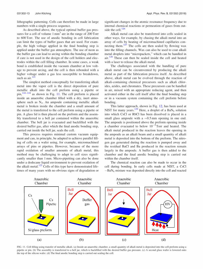
pin,122–124 as shown in Fig. 11. The cell preform is placed
inside an anaerobic chamber filled with a dry, inert atmo-
sphere such as N2. An ampoule containing metallic alkali
metal is broken inside the chamber and a small amount of
the metal is transferred to the cell preform using a pipette or
pin. A glass lid is then placed on the preform and the assem-
bly transferred to a bell jar contained within the anaerobic
chamber. The bell jar is evacuated and backfilled with the
desired buffer gas, after which the final anodic bonding step,
carried out inside the bell jar, seals the cell.
This process requires minimal custom vacuum equip-
ment and can, in principle, be adapted to achieve parallel fill-
ing of cells on a wafer using, for example, micromachined
arrays of pins or pipettes. However, because of the more
rapid oxidation of smaller amounts of alkali metal, this
method may be challenging to adapt to cell sizes signifi-
cantly smaller than 1 mm. Micro-pipetting can also be done
under a dodecane liquid environment to prevent oxidation of
the alkali metal.125 Cells of this type have demonstrated life-
times of many years with no obvious signs of degradation or
significant changes in the atomic resonance frequency due to
internal chemical reactions or permeation of gases from out-
side the cell.126
Alkali metal can also be transferred into cells sealed in
other ways, for example, by chasing the alkali metal into an
array of cells by heating of micromachined capillaries con-
necting them.127 The cells are then sealed by flowing wax
into the filling channels. Wax can also be used to coat alkali
metal droplets into “micropackets,” which can be handled in
air.128 These can then be sealed inside the cell and heated
with a laser to release the alkali metal.
The challenges associated with the handling of pure
alkali metal can be circumvented by producing the alkali
metal as part of the fabrication process itself. As described
above, alkali metal can be evolved through the reaction of
alkali-containing chemical precursors such as alkali chlor-
ides, azides, and chromates. These precursors can be handled
in air, mixed with an appropriate reducing agent, and then
activated either in the cell itself after the final bonding step
or in a vacuum system containing the cell preform before
bonding.
This latter approach, shown in Fig. 12, has been used at
NIST for many years.129 Here, a droplet of a BaN6 solution
into which CsCl or RbCl has been dissolved is placed in a
small glass ampoule with a �0.5 mm opening in one end.
The ampoule is positioned above the preform opening inside
a chamber evacuated to below 10�5 Torr and heated. The
alkali metal produced in the reaction leaves the opening in
the ampoule as an alkali beam and a small quantity of alkali
metal is deposited into the bottom of the preform. The nitro-
gen gas generated during the reaction is pumped away and
the residual BaCl and Ba produced in the reaction remain
largely in the ampoule. A buffer gas is then added to the
chamber and the final anodic bonding step is carried out
within the chamber itself.
The chemical reaction can also be made to occur in the
cell during bonding. In early cells made at NIST, a CsCl
�BaN6 mixture was deposited directly into the cell and reacted
FIG. 11. Cell filling using transfer of metallic alkali. (a) Inside an anaerobic chamber, a small quantity of alkali metal is deposited into the cell preform using a
pipette or pin. (b) The assembly is transferred to a bell jar, which is backfilled with the desired buffer gas pressure. (c) A second glass wafer is lowered onto
the top of the silicon wafer. (d) The final anodic bonding step is carried out sealing the cell.
031302-13 John Kitching Appl. Phys. Rev. 5, 031302 (2018)

as part of the anodic bonding step.122 Cells made in this manner
were found to have an unacceptably high drift of the atomic
hyperfine resonance frequency129 as a result of changing buffer
gas pressure, and this method was therefore abandoned in favor
of the ampoule method described above.
The Cs2CrO4 reaction described above produces much
less residual gas, and hence is better suited to in-situ activa-
tion. Cells have been fabricated100,130 by placing a small
pill131 of ðCs2MoO4Þ=Zr=Al (or ðCs2CrO4Þ=Zr=Al) inside
the vapor cell preform before bonding, as shown in Fig. 13(a).
The cell is then sealed under vacuum or the desired buffer gas
mixture. After sealing, the cell is removed from the chamber
and the pill is illuminated with light from a high-power
laser, which heats the pill to its reaction temperature and
releases the alkali metal. A photograph of such a cell is shown
in Fig. 13(b).
This cell fabrication method is simple and avoids the
somewhat complex deposition inherent to the processes
described above. Since the pill is stable in air, it can be
handled conveniently and the vacuum system need only be
able to perform anodic bonding. This process has been
adapted for wafer-level fabrication in a commercial anodic
bonding machine.121 Upon reaction, the pill getters N2,
implying that N2 cannot be used as a buffer gas. As men-
tioned previously, N2 is a commonly used buffer gas due to
its ability to non-radiatively quench the alkali excited state
population and hence reduce the effects of radiation trap-
ping. However, gases other than N2, such as Ne or Ar, can be
used and appropriately temperature compensated.
A turning point in the buffer gas collisional shift as a func-
tion of temperature has been demonstrated with a Ne buffer
gas alone at a temperature of 80 �C, independent of the Ne
density.132 The turning point temperature can be increased133
above 80 �C through the addition of He. Diffusion of He out of
the cell (through the borosilicate glass windows) resulted in a
substantial frequency drift, �5� 10�9/day, which could possi-
bly be alleviated by the use of different glasses as described
below.
FIG. 12. Ex-situ cell fabrication using chemical reaction outside the cell volume. (a) Inside a high vacuum chamber, alkali metal is created through a chemical
reaction in an ampoule suspended above the cell. (b) The alkali metal is deposited into the cell preform in an atomic beam. (c) A buffer gas is added and the
cell lid is placed on the top surface of the silicon. (d) Anodic bonding is carried out in the vacuum chamber.
FIG. 13. Fabrication of microfabricated alkali vapor cells using compounds of ðCs2MoO4Þ=Ti=Al. (a) Filling method. Reprinted with permission from L.
Nieradko et al., J. Micro/Nanolithogr. MEMS MOEMS 7, 033013 (2008). Copyright 2008 SPIE. (b) Photograph of finished cell. Reprinted with permission
from A. Douahi et al., Electron. Lett. 43, 279–280 (2007). Copyright 2007 the Institute of Engineering and Technology.
031302-14 John Kitching Appl. Phys. Rev. 5, 031302 (2018)

The ðCs2MoO4Þ=Zr=Al mixture can also be mixed with
a paste-like binder material and deposited into cells using an
automated epoxy dispensing tool, allowing for much faster
deposition of the required materials.134 In cells filled using
this method containing a Ne buffer gas alone, a frequency
drift below 5� 10�12/day was measured,134 indicating that
there are no significant changes in buffer gas pressure occur-
ring due to the presence of the unreacted precursors. A simi-
lar fabrication process was developed that used an alkali
dichromate in a titanium tablet.135
Ex-situ filling of cells has also been demonstrated,136 in
which an alkali metal dispenser containing an alkali chromate/
molybdate is situated above the cell preform and the alkalis
are deposited as a thermal beam through a shadow mask.
Many types of glass contain alkali atoms, usually origi-
nating from an alkali carbonate added to the glass precursors
to control the melting point of the glass. These alkali atoms
can diffuse in the glass at elevated temperature and in the
presence of an electric field; it is this process that enables,
for example, anodic bonding. Microfabricated alkali vapor
cells have been made137 by first creating a glass containing a
substantial amount of Cs by heating a mixture of cesium car-
bonate and boron oxide to form a strongly cesiated glass.
Pieces of this glass were then placed inside the Si-glass pre-
form and the cell sealed in an argon atmosphere. The cell
was heated to melt the cesiated glass onto the inner surface
of the borosilicate glass window, and a high voltage was
then applied across the glass from a NaNO3 electrode. Na
ions diffused into the glass, displacing the Cs, which accu-
mulated in solid form on the top window of the cell and
formed a vapor. This process is shown in Fig. 14.
The decomposition of alkali azides has been also used to
fabricate MEMS vapor cells. In an early demonstration,138
CsN3 was deposited into a silicon/glass preform through a
shadow mask, as shown in Fig. 15. The CsN3 was thermally
evaporated with a very slow heating rate to avoid self-
heating and possible explosion during deposition. After
anodic bonding of the second wafer, the cell was extracted
from the deposition chamber and irradiated with ultra-violet
light to dissociate the CsN3 and release Cs and N2. The final
pressure of the N2 gas, which served as a buffer gas, could
be controlled through the irradiation time.
Further work139 showed that the CsN3 could be easily
deposited inside the cells with good uniformity by first dis-
solving it in water and pipetting it into the cell preforms and
that the UV irradiation time could be reduced to a few
minutes instead of several hours by using a UV laser rather
than a lamp. Finally, the alkali azide solution can be depos-
ited on a microstructured material with large surface area to
improve deposition consistency and efficiency and lower the
reaction temperature.140,141
One challenge with the alkali azide cell filling method is
that the final quantity of alkali metal is limited by stoichiom-
etry and the desired buffer gas pressure. For example, if one
atmosphere of N2 is desired in a 1 mm 87Rb cell, only 1 lg of
Rb is produced, which can subsequently be lost due to reac-
tions inside the cell or diffusion into the cell walls at elevated
temperature. It has been found that thin coatings of Al2O3
applied to the interior widow surfaces by atomic layer depo-
sition could improve142 the lifetime of the alkali metal inside
a microfabricated cell at elevated temperatures by a factor of
100. It was also found that anodic bonding could be done
without having to remove the Al2O3 coating from the bond-
ing surface of the glass. A more detailed assessment of the
long-term physical stability of cells with Al2O3 coatings
filled using the CsN3 method was carried out.143 By measur-
ing the size of the alkali metal droplets observed on the
inside glass surface of a microfabricated vapor cell as a func-
tion of time, it was determined that roughly 1 lg of alkali
metal would suffice for a cell operated at 95 �C for 10 yr.
An important aspect of vapor cells used in atomic clocks
is the stability of the buffer gas pressure over long periods.
As described above, small changes in the pressure can lead to
drifts of the clock output frequency through the pressure shift.
The gas pressure can change if chemical reactions occur in
FIG. 14. Electrolytic fabrication of microfabricated alkali vapor cells.
Reprinted from Rev. Sci. Instrum. 77, 076101 (2006). Copyright 2006 AIP
Publishing LLC.
FIG. 15. Microfabricated alkali vapor cells filled using ultra-violet decom-
position of CsN3. Reprinted with permission from L.-A. Liew et al., in
Proceeding of Eurosensors (2007). Copyright 2007 AIP Publishing LLC.
031302-15 John Kitching Appl. Phys. Rev. 5, 031302 (2018)

the vapor cell or if gases such as He leak into or out of the
cell through the windows. Measurements of the long-term sta-
bility of the buffer gas in cells filled with the pipette method
shown in Fig. 11 showed126 a frequency drift of 1.7� 10�13/
day in a clock incorporating such a cell after several years of
operation. Cells fabricated using the alkali molybdate dissoci-
ation method have also been measured in a clock configura-
tion144 and showed a frequency drift of �5� 10�11/day,
consistent with slow permeation of the Ne buffer gas out of
the cell through the glass windows.
D. Alternative cell geometries
It is sometimes the case that it is useful, particularly in
the case of magnetometry, to have optical fields propagating
in the cells in orthogonal directions. Cell geometries with two
planar glass windows are cumbersome to use in this case,
since the orthogonal beams must pass through the cell at an
angle with respect to the cell surface. Several approaches
have been developed to address this issue. A novel type of
spherical cell geometry has been developed,145,146 in which
small glass bubbles were blown from blind cavities etched in
silicon and capped with glass, as shown in Fig. 16. The silicon
backside was then etched out to allow access to the cell inte-
rior and the cells filled with alkali metal using the deposition
method shown in Fig. 12. These cells are particularly useful
for NMR gyros where the self-field of the polarized noble gas
in non-spherical cells can create important systematics.
Cells have also been fabricated with angled interior walls
that can reflect light incident normal to the cell window sur-
face into the transverse direction. The natural etch angle of
silicon is 54.7� and it is therefore straightforward to fabricate
cells with the interior walls at this angle using standard chem-
ical etching. Cells with such angled sidewalls with dielectric
anti-reflection coatings have been demonstrated.147,148 The
54.7� angle of the silicon walls does not allow reflection of a
vertical beam into the horizontal plane. However, it is possi-
ble to incorporate grating structures on the input windows to
diffract the light entering the cell by an angle such that hori-
zontal propagation is achieved after reflection from the silicon
sidewall,149 as shown in Fig. 17.
While anodic bonding has in most cases been used to
fabricate small vapor cells with dimensions on the order of
1 mm, the approach has also been adapted for larger vapor
cells. It is challenging to etch through thick silicon wafers
without damaging the surface polish and hence reducing the
yield of the anodic bonding step. In order to make larger
cells, a glass interposer with a hole drilled through it can be
bonded to two etched silicon wafers, onto which the glass
windows are bonded in turn.150 GaP can also be used as the
wall of the cell preform151 if high thermal conductivity and
low helium permeation are required. Glass can be bonded
onto GaP at about 200 �C, making this material useful for
low-temperature cell filling also. Finally, anodic bonding
between glass and sputtered SiN can enable the integration
of metal feedthroughs into microfabricated alkali vapor
cells.152 The application of this approach to a triple-stack
anodically bonded cell is shown in Fig. 18. In this process,
the layers being bonded are all glass. Cr electrodes are
deposited on the upper and lower glass layers and run from
inside to outside the cell. A 200 nm SiN layer is deposited
over the Cr and onto the glass where the Cr has been etched
away to form a rim matching the walls of the middle glass
layer to which the SiN is anodically bonded.
Since lithographic patterning and etching is used to
define the cell geometry on the surface of a silicon wafer,
parallel processing can enable the fabrication of many cells
FIG. 16. Micro-glassblown alkali vapor cells. Reprinted with permission
from E. J. Eklund et al., Sens. Actuators A 143, 275–280 (2008). Copyright
2008 Elsevier.
FIG. 17. Generation of horizontally propagating beams in a micromachined
vapor cell using diffraction gratings on the input window. Reprinted with
permission from R. Chutani et al., Sci. Rep. 5, 14001 (2015). Copyright
2015 Author(s), licensed under CC BY.
FIG. 18. Triple-stack anodic bonding of glass wafers using a sputtered SiN
layer. This approach allows metallic electrical feedthroughs to extend from
outside to inside the cell. In this visualization, the view is looking at one of
the cell walls from the side, with the Cr electrodes extending out of and into
the page. Reprinted with permission from Appl. Phys. Lett. 105, 041107
(2014). Copyright 2014 AIP Publishing LLC.
031302-16 John Kitching Appl. Phys. Rev. 5, 031302 (2018)

on a single wafer using a single process sequence. The fabri-
cation of cells in arrays was demonstrated quite early with
the pipetting cell fabrication technique.124 Processes have
also been developed to separate and thermally isolate cells,
while maintaining the rigidity of the array spacing by using a
common window for all cells in the array.139 Finally, multi-
ple cells can be connected by channels to the same reservoir
to form arrays of cells with the same buffer-gas pressure,153
as shown in Fig. 19. Magnetometer arrays based on this
multi-cell approach have also been demonstrated for mag-
netic gradiometry and imaging.153 Glass cells with thick-
nesses between 20 lm and 200 lm have also been fabricated
using lithographic glass etching techniques.154
E. Alternatives to anodic bonding
One of the challenges associated with cell fabrication
using anodic bonding is that the cell must usually be heated
to near 300 �C. This requirement has been a major limitation
in, for example, the development of microfabricated cells
with a wall coating instead of a buffer gas to suppress wall
relaxation. Many wall coatings, such as paraffin, are unable
to withstand temperatures substantially above 100 �C and
therefore are destroyed during the anodic bonding process.
Microfabricated alkali vapor cells have therefore been
recently developed that use a low-temperature solder on sili-
con155 or low-temperature cofired ceramic125 for sealing,
rather than anodic bonding, as shown in Fig. 20. In Ref. 155,
thermocompression bonding at 140 �C was used to seal a
cell, the interior of which was coated with octadecyltrichlor-
osilane (OTS), which is stable up to 170 �C in the presence
of alkali vapor.156 This cell showed a hyperfine resonance
linewidth of under 10 kHz, suggesting that the wall coating
was acting effectively to prevent depolarization. Low tem-
perature anodic bonding techniques have also been devel-
oped, and silicon/glass alkali vapor cells have been
fabricated by bonding at temperatures as low as room
temperature.157 In these cells, the low-temperature bonding
was enabled by a �1 lm layer of lithium-niobate-phosphate
glass, which has a very high ionic conductivity and was
deposited onto one surface of the second glass wafer. Cells
have also been fabricated158 using Cu-Cu thermocompres-
sion bonding, which may allow the use of different substrate
materials.
Glass frits have also been used to seal potassium atoms
and buffer gas inside an evacuated enclosure.101,140 In this
process, small channels �10 lm in cross-sectional size and
�1 mm long are etched in a silicon frame to connect the
inside of an etched silicon cavity with the outside. A Bi2O3-
B2O3 frit with a softening temperature below 400 �C is then
deposited in a frame pattern on a glass wafer to be used as
the lid. Alkali precursors (in this case, KCl and Ca) are
placed inside the cavity and the glass lid placed over the cav-
ity such that the frit is situated over the channels. The alkali
source is activated at 450 �C under vacuum, any gas pro-
duced in the reaction is pumped away through the channels,
and the chamber is then backfilled with the desired buffer
gas. Finally, the lid is pressed against the silicon wafer at
480 �C and the frit reflows into the channels creating a her-
metic seal. This process was demonstrated in �1 cm glass
cells, but should be easily adaptable to microfabricated cells.
There are several factors that traditionally contribute to
the long-term frequency drift of vapor cell atomic clocks.
The two most important factors are small changes in the
buffer gas pressure due to leakage or diffusion through the
cell walls and light shifts due to the slowly varying inten-
sity of the interrogation light. The use of non-traditional
materials and cell-filling processes raises the possibility
that the drift of microfabricated alkali vapor cells could be
significantly different from traditional glass-blown cells. In
Table I, the measured drift rates for some microfabricated
cells fabricated under a variety of conditions are listed. The
best drift rate obtained so far is �8� 10�13/day for a cell
packaged in an evacuated enclosure after several months of
operation. The long-term ageing of a number of commercial
chip-scale atomic clocks deployed on the ocean floor has
been monitored over a period of several years.159
FIG. 19. Many alkali vapor cells can be connected to the same alkali reser-
voir to form cell arrays useful in, for example, magnetic imaging. Reprinted
with permission from Rev. Sci. Instrum. 83, 113106 (2012). Copyright 2012
AIP Publishing LLC.
FIG. 20. Schematic of a process for microfabricating silicon/glass alkali
vapor cells based on an indium seal. Reprinted with permission from Appl.
Phys. Lett. 105, 043502 (2014). Copyright 2014 AIP Publishing LLC.
031302-17 John Kitching Appl. Phys. Rev. 5, 031302 (2018)

Significant variation in the ageing behavior was observed
from clock to clock, but the best units demonstrated ageing
at or below 2� 10�12/day.
III. MEMS-BASED ATOMIC CLOCKS
A. Introduction
Throughout the 1990s, considerable effort was spent at
companies around the world developing compact atomic
clocks. This was driven largely by the cellular telephone
industry, which was installing atomic clocks in cell-phone
base stations to provide holdover timing in the event of a
failure of the GPS timing system.48 The baseline timing
requirement for synchronization of cell-phone networks was
an error of no more than 10 ls over one day. Clocks were
developed with a volume of �100 cm3 and operating on
�10 W of power for this purpose. While these clocks served
the cell phone industry needs well, they consumed too much
power to allow them to be integrated into portable, battery-
operated instruments.
With the proliferation of handheld consumer and mili-
tary GPS receivers, it was realized that battery-powered
atomic frequency references that could be integrated into
such receivers could provide significant benefits to satellite-
based navigation.162–164 This, along with the potential
application to secure wireless communications, was a strong
motivation to begin the development of significantly lower
power vapor cell clocks.
The use of VCSELs in atomic clocks was pioneered by
a group at Westinghouse (now Northrup-Grumman) through-
out the 1990s.85 Their goal was to reduce the power con-
sumption and size of a vapor cell clock using laser
technology in place of the discharge lamp. Using miniature
glass-blown vapor cells85,165 in small microwave cavities,
they achieved a clock short-term stability ry sð Þ <2� 10�11=�s and long-term drift of 3� 10�12 at 104 s in a
physics package with a volume of 16 cm3 running on a few
hundred mW of electrical power.
This section deals with the development of atomic
clocks incorporating silicon micromachined vapor cells as
described above. The use of micromachining enabled the
development of millimeter-scale physics packages that could
be well thermally isolated from the environment and hence
required very little power to heat. This, along with the use of
VCSELs for the light source and the development of low-
power RF synthesizers and control electronics, were the
three key elements that enabled chip-scale atomic clock
(CSAC) technology to succeed.
TABLE I. Drift rates measured in microfabricated vapor cells.
Reference Alkali filling method Buffer gas Drift Temperature (�C) Notes
160 In situ BaN6þCsCl 150 Torr N2/Ar �2� 10�8/day 85 Attributed to internal cell chemistry
129 Ex situ BaN6þRbCl Not stated �5� 10�11/day 90 Probably limited by cell tempco
161 Pure Cs (glovebox) Not stated �8� 10�11/day 80 Initial 20 days
161 Pure Cs (glovebox) Not stated �8� 10�13/day 80 After 100 days of operation
133 In situ 2Me2CrMbþ Zr3Al2 He/Ne �5� 10�9/day 94.6 Possibly due to He leakage out of cell
144 In situ 2Me2CrMbþ Zr3Al2 100 Torr Ne �5� 10�11/day 81 Consistent with Ne diffusion through glass
118 Ex situ BaN6þRbCl 200 Torr Ar/N2 1.8� 10�7/day 96 In chamber containing 500 Torr He; borosilicate glass
118 Ex situ BaN6þRbCl 200 Torr Ar/N2 9� 10�10/day 91 In chamber containing 500 Torr He; aluminosilicate glass
134 In situ 2Me2CrMbþ Zr3Al2 paste 60 Torr Ne �4� 10�12/day 75
FIG. 21. (a) Conceptual design of a chip-scale atomic clock physics package. Reprinted with permission from L. Hollberg and J. Kitching, U.S. patent
6,806,784 B2 (2004). (b) Estimated stability as a function of cell size for a wall coating with NB ¼ 500 (black line) and a N2 buffer gas at P¼ 76 Torr (red
line). Adapted from Appl. Phys. Lett. 81, 553–555 (2002). Copyright 2002 AIP Publishing LLC.
031302-18 John Kitching Appl. Phys. Rev. 5, 031302 (2018)

B. Design considerations
At the heart of any atomic frequency reference lies the
physics package. This subsystem comprises at a minimum
the alkali vapor cell, excitation and detection components,
such as the light source and photodetector, and all the optical
components. In large part, the physics package determines
both the short- and long-term frequency instabilities of the
clock. It also contributes directly to the size and power dissi-
pation of the frequency reference. We discuss here several
key considerations that impact the design of MEMS-based
physics packages.
Some early suggestions of batch-fabricated atomic
clocks centered on the idea of using etchable ceramics to
form the gas cell and application-specific integrated circuit
(ASIC) technology for the control electronics,165 with the
goal of producing a $100 atomic clock that could hold 10 ns
over 1 day. More specific designs for a chip-scale atomic
clock and magnetometer physics package113 envisioned an
anodically bonded silicon/glass microfabricated alkali vapor
cell coupled to a vertical-cavity surface-emitting laser in
which the atoms were excited using coherent population
trapping, as shown in Fig. 21(a).
Under some assumptions with respect to the signal
amplitude and noise, it is possible to project the achievable
Allan deviation as a function of cell size for a clock based on
coherent population trapping,166 as shown in Fig. 21(b). For
cell sizes between 100 lm and 1 mm, short-term frequency
stabilities near 10�10 at 1 s can, in principle, be achieved.
The degradation of the frequency stability at small cell sizes
arises for two main reasons. First, the transition linewidth
increases, as shown in Fig. 2, due to increased collision rate
with the cell walls and the buffer gas. Second, the cross-
sectional area of the interrogating light field drops, leading
to a smaller detected photon flux and hence a reduced signal
to noise ratio. It is assumed here that the cell temperature is
adjusted for constant optical absorption as a function of cell
size and spin-exchange collisional broadening is ignored.
The stability degrades as 1=R3=2 under optimal buffer gas
pressures and if the detection noise is limited by photon shot
noise, as shown in Fig. 21(b).
The power required to run the physics package can be sep-
arated by component. Most commercially available VCSEL
light sources require about 5 mW of power. However, it should
be noted that VCSELs with threshold currents well below
1 mA have been reported and the use of such devices may
therefore allow operation of a CSAC at considerably lower
powers. The laser must also be temperature-stabilized to be
able to lock the laser wavelength onto the atomic optical transi-
tion while avoiding large variations in output power. All viable
CSAC designs produced so far have avoided the use of active
cooling (with thermoelectric coolers, for example) in the ther-
mal design, due to the inefficiency of this process. The laser is
instead stabilized at a temperature above the maximum ambi-
ent temperature using only heating elements. Since the lifetime
of a laser gets shorter as its operating temperature is increased,
there is potentially a tradeoff between the lifetime of a chip-
scale atomic clock and its operating temperature range.
Accelerated lifetime testing89 of VCSELs developed for
CSAC applications suggests that device lifetimes over 6 yr are
reasonable for operating temperatures of 85 �C.
The cell must also be temperature stabilized to reduce
temperature-dependent frequency shifts due to collisional
processes within the cell. With temperature compensated
buffer gas mixtures of a few hundred Torr, a temperature sta-
bility of �0.1 K is required to maintain a fractional fre-
quency stability of 10�12. While the cell temperature must
also be maintained above the maximum ambient temperature
for the same reasons as the laser, an additional requirement
is that the atom density in the cell be sufficient to produce a
good CPT signal. For cells based on 133Cs or 87Rb of length
1 mm, a cell temperature in the range of 80 �C to 100 �C is
optimal for conventional CPT interrogation. It is somewhat
fortuitous that this temperature range fits well with the
requirement related to the maximum ambient temperature.
The power radiated by a black body at temperature Tcell
into an ambient temperature Tamb is given by the Stefan-
Boltzmann law as
Prad ¼ �rA T4cell � T4
amb
� �; (19)
where � is the surface emissivity, r is the Stefan-Boltzmann
constant, and A is the surface area of the cell. For a cubic
cell, this radiated power is plotted as a function of side length
L for an emissivity of unity in Fig. 22. For a radiated power
below 10 mW, the cell (or whatever parts of the physics
package are hot) must be on the order of 1 mm in size. In
addition, the cell must be sufficiently well thermally isolated
that conduction and convection losses are small.
Because of the high operating temperatures of the cell
and the laser, thermal isolation of both components is critical
in achieving low power dissipation. In some designs,160 the
cell and laser are controlled independently, while in others,124
they are controlled together at the same temperature. It should
be noted that the thermal resistance cannot be made too high
due to the presence of heat sources inside the physics pack-
age. The largest of these results from the DC current required
to run the laser. The wall-plug efficiency of most VCSELs is
in the range of 20%; most of the electrical power that drives
the VCSEL therefore ends up as heat. If the thermal resistance
FIG. 22. Radiated power into a 0 �C ambient as a function of cell size for
three different cell temperatures.
031302-19 John Kitching Appl. Phys. Rev. 5, 031302 (2018)

between the laser and package wall is too high, the physics
package will overheat at high ambient temperatures simply
due to this internal heat source. One way of solving this prob-
lem is to use a thermal link with a variable thermal resis-
tance.167 While such techniques have yet to be demonstrated
in chip-scale atomic devices, they represent a compelling pos-
sibility for future design improvements.
A final key consideration is manufacturability and
device cost. Because of the possibility for wafer-level proc-
essing and integration, micromachining techniques offer
considerable advantage here if high device volumes are
needed. Ideally, the physics package should have a simple
design, such that either the entire physics package can be
fabricated on a single wafer or the individual components
can be fabricated and integrated in wafers. In either case, the
result is that large numbers of physics packages can be fabri-
cated with the same process sequence.
C. Physics packages
The MEMS-based atomic clock physics package dem-
onstrated in 2004 at NIST160,168 is shown in Fig. 23. This
device was vertically integrated, in the sense that the light
beam propagated in a direction perpendicular to the substrate
surface and components were integrated by stacking layers,
one on top of the other. At the lower end of the device, a
vertical-cavity surface-emitting laser was mounted onto a
custom substrate of gold traces patterned on a rigid insulator
(AlN, in this early design). A series of optics layers were
positioned over the laser and held off the surface by a dual
strip isolator. The optics included two neutral density filters,
which attenuated the light beam to about 10 lW, a micro-
lens, which collimated the beam to a diameter of about
250 lm, and a quarter-wave plate, which converted the light
polarization from linear to circular.
The cell and heater assembly was mounted on top of the
optics assembly. The cell heaters were pieces of thin glass
with a thin layer of indium-tin oxide (ITO) deposited on the
surface. ITO is a commonly used transparent, conductive
material, and useful here since it allows light to pass through
the windows of the cell while at the same time allowing for
resistive heating via current flow along the window surface.
The cell itself was fabricated with the in-situ MeCl/BaN6
technique described above and had external dimensions of
1.5 mm� 1.5 mm� 1.4 mm. The heaters were wire-bonded
to gold traces on the substrate with gold wires with a diame-
ter of 25 lm. Finally, a photodetector was placed on the very
top of the structure to monitor the light transmitted by the
cell. The complete structure was 4.2 mm tall and had a
square cross-section of 1.5 mm, leading to a total volume of
less than 10 mm3.
This first device, based on Cs atoms excited on their D2
line, had a resonance linewidth of 7 kHz and a measured
short-term frequency instability of 3� 10�10/�s. The long-
term frequency drift was quite large compared to larger
vapor cell frequency references at 1.6� 10�8/day. The reso-
nance linewidth, frequency as a function of time, and corre-
sponding Allan deviation are shown in Fig. 24. The physics
package operated on 75 mW of electrical power at an ambi-
ent temperature of 46 �C.
FIG. 23. A microfabricated atomic clock physics package. (A) Schematic of
assembly. Layers from bottom to top: a, Glass (500 lm); b, Spacer
(375 lm); c, ND filter (500 lm); d, Glass (125 lm, not shown); e, Quartz
(70 lm, not shown); f, ND filter (500 lm); g, Glass/ITO (125 lm/30 nm); h,
Glass (200 lm); i, Si (1000 lm); j, Glass (200 lm); k, Glass/ITO (125 lm/
30 nm); l, Si (375 lm); and m, Glass (125 lm). Total height: 4.5 mm; width
and depth: 1.5 mm. Photographs (B) photodiode assembly, (C) cell assem-
bly, (D) optics assembly, (E) laser assembly, and (F) the full atomic clock
physics package realized as a microchip. The black lines in the photographs
indicate 1 mm. Reprinted with permission from Appl. Phys. Lett. 85,
1460–1462 (2004). Copyright 2004 AIP Publishing LLC.
FIG. 24. Performance of an early chip-scale atomic clock physics package. (a) CPT resonance. The contrast here is defined as the ratio of the change in absorp-
tion due to the CPT effect to the total absorption. (b) Output frequency of a large-scale local oscillator locked to the CSAC physics package, as a function of
time. (c) Allan deviation calculated from the data in (b). Reprinted with permission from Appl. Phys. Lett. 85, 1460–1462 (2004). Copyright 2004 AIP
Publishing LLC.
031302-20 John Kitching Appl. Phys. Rev. 5, 031302 (2018)

Several improvements to this device were demonstrated.
First, the short-term frequency stability was improved by
building a device that could be excited on the D1 line.169 It
is known that CPT resonances based on D1 excitation in
vapor cells have considerably larger contrast and therefore
result in better clock frequency stability.169–171
The large frequency drift in the CSAC physics package
shown in Fig. 24 was most likely due to chemistry internal to
the cell. The cell in this device was filled by depositing the
CsCl/BaN6 precursors into the cell itself and initiating the
reaction to produce the Cs during the bonding process. As a
result, the reactants remained in the cell after sealing. The
drift was eliminated129 at a level considerably below 10�10/
day through the atomic beam deposition technique. Other
cell-filling techniques have demonstrated even better long-
term frequency stabilities.172–174
A major improvement in the power dissipation of CSAC
physics packages was reported in Ref. 124. In this design,
shown in Fig. 25, the physics package was suspended from
thin polyimide tethers, on which metal traces were deposited
to electrically connect the physics package with the control
system. This suspension had a thermal conductance of only
0.14 mW/K, which allowed essentially radiation-limited
operation at a cell temperature approaching 100 �C when
vacuum packaged. A physics package based on this design
has demonstrated172 a short-term fractional frequency insta-
bility of near 2� 10�11/�s while running on less than 10
mW at an ambient temperature of 25 �C. Similar thermal iso-
lation solutions have been used in other designs to achieve
comparably low power dissipation.173,174 The CSAC design
shown in Fig. 25 included several other novel features. The
physics package was based on a folded optics geometry [see
Fig. 25(a)], in which diverging light emitted by the laser
passed through the cell was reflected off a mirror and passed
back through the cell a second time before being detected
with a photodetector in the same plane as the laser. This dou-
bled the interaction length and increased the signal strength.
A novel integrated laser/photodetector89 was also developed
for this design.
A second vertically integrated design is shown in
Fig. 26. In this design, size is again reduced by allowing the
laser beam to expand in a folded geometry. The laser is
mounted such that it initially propagates away from the
vapor cell. A dual focus optic combined with a mirror allows
the transverse beam profile to expand such that it fills the
vapor cell in a much smaller longitudinal distance that it
would otherwise.
A physics package design that relies more heavily on
advanced MEMS processing175 is shown in Fig. 27. In this
design, light from a VCSEL is redirected by a mirror etched
in Si into the horizontal plane. The light then passes through
FIG. 25. A CSAC physics package design with a power dissipation below 10
mW. (a) Physics package design showing the physics package mounted on pol-
yimide thermal isolation tethers and the folded optics design. (b) A photograph
of completed physics packaged in polyimide suspension system. Reprinted
with permission from R. Lutwak et al., in Proceeding of Precise Time andTime Interval (PTTI) Meeting (2004), pp. 339–354.
FIG. 26. A vertically integrated CSAC physics package. (a) Physics package
design with folded geometry and (b) photograph of the assembled physics
package, with shielding removed. Reprinted with permission from J. F.
DeNatale et al., in Proceeding of IEEE Position Location and NavigationSymposium (PLANS) (2008), pp. 67-70. Copyright 2008 IEEE.
031302-21 John Kitching Appl. Phys. Rev. 5, 031302 (2018)

some optics and into a vapor cell suspended in vacuum by
thin, thermally isolating bridges. The light is redirected
toward the photodetector by a second angled mirror. The cell
in this design is formed by deep reactive ion etching (DRIE)
and is sealed after filling with a reflow solder. The advantage
of this design is that essentially all components can be etched
into only three wafers, which are then bonded together to
assemble the physics package.
A second horizontally integrated design was pro-
posed,176 in which the top and bottom plates that confine the
alkali metal in the cell are sealed by anodic bonding. This
design uses conventional excitation of the atomic resonance
by integrating a stripline waveguide onto the top of the cell
assembly. A laser diode is proposed as the light source.
Thermal isolation in most chip-scale atomic devices is
achieved by mounting the heated components in an evacu-
ated package and suspending them on thin tethers, which
limits the heat conduction to the package walls. The tethers
have been fabricated from a polyimide,124 shown in Fig. 25,
or from glass, as shown in Fig. 28. The cells are heated with
a current flowing in metallic traces patterned on the cell sur-
face and the tethers. Heating can also be done by flowing
current through etched, doped silicon, fabricated either as
part of the cell177 or mounted externally after cell fabrica-
tion.178 In one considerably simpler design, shown in Fig.
29, a chip-scale physics package was mounted on a
polytetrafluoroethylene (PTFE) pillar for thermal isolation
and packaged inside an evacuated container.179 The physics
package could be heated to 100 �C using 150 mW of electri-
cal heating power.
D. Compact, low-power local oscillators
In a passive atomic frequency standard, the frequency
stability of the local oscillator is important from several per-
spectives. First, the overall stability of the oscillator must be
low enough that the servo system can lock the oscillator to
the atomic transition. Sudden jumps in the (unlocked) oscil-
lator frequency, for example, may be beyond the locking
range of the servo loop and therefore bring the oscillator out
of lock. Second, the phase noise of the oscillator at frequen-
cies larger than the servo bandwidth must be consistent with
the application for which the clock is intended. Finally, the
phase noise of the oscillator at all even harmonics of the
servo modulation frequency can create instability in the
locked frequency over long integration times as a result of
aliasing.180 Usually, the noise at the second harmonic domi-
nates, in which case, this last requirement can be simply
stated for white frequency noise as
Sy 2fmð Þ < 4sry sð Þ2; (20)
where Syð2fmÞ is the power spectral density of the fractional
frequency fluctuations at twice the modulation frequency,
ry sð Þ is the desired Allen deviation, and s is the integration
time.
For chip-scale atomic clocks, the oscillator must satisfy
several other conditions. First, it must be tunable to a subhar-
monic of the hyperfine frequency of the atom being interro-
gated. Usually the first subharmonic (4.596 GHz for 133Cs
and 3.405 GHz for 87Rb) is a good compromise between con-
venience and performance. It must also be tunable with an
FIG. 27. Horizontally integrated design for a chip-scale atomic clock phys-
ics package. (a) Schematic of physics package and (b) photograph of vapor
cell integrated into optical path. Reprinted with permission from D. W.
Youngner et al., in Proceeding of IEEE Transducers (2007), pp. 39–44.
Copyright 2007 IEEE.
FIG. 28. Alkali vapor cell suspended on glass tethers to thermally isolate the
heated cell from the walls. Reprinted with permission from D. W. Youngner
et al., in Proceeding of IEEE Transducers (2007), pp. 39–44. Copyright
2007 IEEE.
031302-22 John Kitching Appl. Phys. Rev. 5, 031302 (2018)

analog or digital control signal over a range large enough to
compensate for all oscillator frequency variations caused by
environment or aging. In addition, about 0.1 mW–1 mW of
RF power is needed to drive the VCSEL and the oscillator
must provide that or amplification must be used. Finally,
most applications require a 5 MHz or 10 MHz clock output
to interface with existing signal channels.
Traditionally, local oscillators for vapor cell atomic
clocks have been based on a 5 MHz or 12.5 MHz quartz crys-
tal oscillator, multiplied up to the alkali transition frequency
(6.8 GHz) by a step recovery diode.17 The oscillator is locked
to the atomic resonance with a frequency-locked loop.
However, step-recovery diodes require considerable input
power to generate the high harmonics necessary to access
the atomic resonance frequencies, making them largely
impractical for low-power instruments.
Fractional-N dividers (or dual modulus prescalers) are a
much lower-power alternative for bridging the frequency
gap between the required 5 MHz output and the GHz-range
atomic transition frequencies. With such a device, a high-
frequency voltage-controlled oscillator (VCO) can be phase-
locked to a 10 MHz quartz oscillator using only a few mW
of power. Thus, fractional-N dividers have been widely used
in chip-scale atomic clocks. The basic architecture of such a
phase-locking circuit, along with the frequency-locked loop
that controls the oscillator frequency, is shown in Fig. 30.
Several types of novel oscillators were developed spe-
cifically for chip-scale atomic clocks. Coaxial waveguide
resonators have been used,181,182 with the gain provided by a
bipolar junction transistor. The resonator had a small form
factor (2 mm� 2 mm� 3.9 mm), low cost, moderately high
Q-factor (�100), and a resonant frequency near 3.4 GHz.
The oscillator produced 0.25 mW of RF power with only 2.1
mW of DC power at 1.2 V and the single sideband phase
noise at 300 Hz was about �55 dBc/Hz.
Oscillators based on thin-film bulk acoustic resonators
(TFRs or FBARs)183,184 were also developed. A Colpitts
oscillator based on a TFR produced 0.25 mW of RF power at
4.6 GHz with 10 mW of DC power.185 The phase noise at
300 Hz was –53 dBc/Hz. A similar oscillator was developed
by Yu et al. VCOs for chip-scale atomic clocks have been
demonstrated using more conventional oscillator
approaches,186 but have yet to achieve low power operation.
In one novel low-power oscillator design,174 a 569 MHz
quartz crystal oscillator was used to directly injection lock a
3.4 GHz VCO. This eliminated the need for a phase-locked
loop entirely, and the power required to run it. The phase
noise at 3.4 GHz was measured to be –92 dBc/Hz at 1 kHz
offset and the oscillator required less than 7 mW to operate.
However, the clock output frequency was 569 MHz and fur-
ther division and corresponding power would be needed to
reach a 5 MHz or 10 MHz output.
Application-specific integrated circuits (ASICs) have been
developed to achieve good oscillator performance at even
lower power. A PLL circuit was implemented187 in 0.18 lm
CMOS and integrated on chip with a transimpedance amplifier
and phase-sensitive detection element for the photodetector sig-
nal. This IC ran on 26 mW, including the RF power amplifier
required to reach 1 mW of RF output power. The phase noise
at 1 kHz offset was –86 dBc/Hz at 3.4 GHz. When locked to an
atomic physics package, this oscillator supported a short-term
frequency stability of 4� 10�10=�s. An even lower power of
12 mW was achieved in another ASIC,188 which also incorpo-
rated high-resolution frequency tuning of 10�13. The phase
noise 1 kHz from the carrier was –83 dBc/Hz and the active
area of this chip was only 0.7 mm2. This chip supported a clock
frequency stability of 5� 10�11 at 1 s of integration. A sche-
matic and photograph of this last chip is shown in Fig. 31.
E. Control electronics
Electronics are required in any vapor cell atomic clock
to power the entire instrument and implement several control
loops that stabilize various instrument parameters. The pri-
mary control loop in a laser-pumped passive atomic standard
is that which stabilizes the local oscillator frequency to the
atomic microwave resonance. Since the quality of this con-
trol loop directly impacts the short- and long-term frequency
stability of the frequency reference, it is the most critical ele-
ment in the control system. Secondary control loops stabilize
the temperature of the vapor cell and laser and lock the laser
wavelength to the atomic optical transition.
FIG. 29. Chip-scale atomic clock in which the physics package is mounted
on a PTFE pillar for thermal isolation. Reprinted with permission from S. L.
Li et al., Chin. Phys. B 23, 6 (2014). Copyright 2014 Institute of Physics,
Chinese Academy of Sciences.
FIG. 30. Architecture of a phase-locked loop based on a fractional-N divider
(in blue) and a frequency-locked loop that controls the oscillator frequency
(in red).
031302-23 John Kitching Appl. Phys. Rev. 5, 031302 (2018)

As described above, the temperature of the vapor cell
determines the signal size (via the alkali vapor density) and
the magnitude of the alkali-buffer gas collision shift. The
cell temperature is usually stabilized by monitoring the cell
temperature with a temperature sensor (thermistor or Pt film)
and then feeding an error signal generated from this mea-
surement back into the cell heaters. Temperature stability of
�10 mK is not difficult to achieve with this method.
The wavelength of the radiation emitted by the laser must
also be tuned and locked to the optical resonance in the atoms
in order to excite the CPT resonance. The wavelength of a
VCSEL can be tuned by changing either the laser temperature
or laser current. Thus, feedback to either temperature or current
could be used to stabilize the laser wavelength. Usually, the
laser temperature is measured with a temperature sensor
located nearby and stabilized to a roughly constant value using
a small heater. The laser current is then modulated at a fre-
quency of a few kHz (thereby modulating the laser wavelength)
and the photodetector signal demodulated synchronously to
generate an error signal. This error signal is then used to adjust
the laser current and stabilize the laser frequency to the peak of
the optical absorption spectrum. This basic locking scheme,
shown in Fig. 32(a), can be modified as described in detail
below.
There are also several tertiary control functions that can be
implemented and that generally lead to improved long-term fre-
quency stability. These include active stabilization of the laser
output power, the RF power going into the laser, and the DC
magnetic field applied to the vapor cell. Control systems for
early atomic frequency references were implemented using ana-
log electronic circuits. The recent development of low-power
microprocessors and field programmable gate arrays (FPGAs)
have allowed the control systems to be implemented instead as
firmware with only a modest analog interface circuit.189–191 This
type of implementation not only reduces power consumption but
also allows considerably more functionality to be included with
only minor design changes to the hardware. Microprocessor-
based control circuits have been demonstrated that run on less
than 30 mW of electrical power, including power regulation.191
A control system was also developed at CSEM based on
application-specific integrated circuit.187 Like the design above,
it was based on a low-power VCO phase-locked to a lower-
frequency VCXO using a fractional-N divider. This chip ran on
only 24 mW of electrical power, with the main sources of
power consumption being the VCO and the output amplifier.
FIG. 31. Application-specific integrated circuit implementation of a local
oscillator for a chip-scale atomic clock. (a) Chip architecture and (b) micro-
graph of chip. Reprinted with permission from Y. Z. Zhao et al., IEEE
Trans. Instrum. Meas. 64, 263–270 (2015). Copyright 2015 IEEE.
FIG. 32. Atom-based stabilization schemes. Reprinted with permission from
V. Gerginov et al., Opt. Lett. 31, 1851 (2006). Copyright 2006 The Optical
Society of America. (a) Conventional stabilization, in which the laser and
cell temperatures are stabilized with thermistors, and the laser wavelength is
stabilized using feedback to the laser injection current from the atomic
absorption resonance. (b) The laser current is driven with a constant current
source and the laser wavelength is stabilized with feedback from the atomic
absorption resonance. (c) The cell temperature is now also stabilized with
feedback from the atomic absorption resonance. (d) A photodiode before the
cell monitors the output power of the laser.
031302-24 John Kitching Appl. Phys. Rev. 5, 031302 (2018)

This chip successfully controlled a clock based on a glass vapor
cell to a short-term stability192 of 4� 10�10=�s.
The basic control architecture described above suffers
from some minor limitations that result in long-term instabil-
ity of the output frequency. One class of limitations involves
temperature gradients between the cell and laser and their
respective temperature sensors. Although the temperature
sensors are typically located as close as possible to the ele-
ment to be controlled, some spatial separation is unavoid-
able, which results in a finite thermal resistance between
them. Even if the sensor temperature is perfectly stabilized,
temperature fluctuations of the cell and laser can therefore
still be present.
As mentioned above, temperature fluctuations of the laser
cause changes in the laser output wavelength. The disadvantage
of the basic scheme shown in Fig. 32(a) is that as the laser cur-
rent is adjusted to maintain a constant wavelength under chang-
ing temperature conditions, the optical power also changes.
Changes in optical power result in changes in the AC Stark
shift and cause secondary fluctuations in the clock output fre-
quency. An alternative, shown schematically in Fig. 32(b), is to
drive the laser current with a constant current source and feed
the laser wavelength error signal back into the laser heater,
thereby eliminating the need for a thermistor near the laser.193
The laser temperature is therefore stabilized directly using the
parameter of interest (the wavelength), rather than indirectly
using a thermistor.
The temperature of the cell can be controlled using a
similar modification, in which the DC absorption of the
alkali atoms is used as a measure of the cell temperature.
Since the alkali vapor pressure depends strongly on tempera-
ture (factor of ten change in density for every �30 K change
in temperature), the optical absorption of the light by the
atoms changes by about 1%/K. The DC signal from the pho-
todiode after the cell can therefore be compared to a prede-
termined voltage and the difference signal sent back to the
cell heater [see Fig. 32(c)]. This again eliminates the need
for a thermistor to monitor the cell temperature, which is
instead stabilized based on the parameter of interest, the
alkali density. A final possible control element is to monitor
the light power level before the cell and feed an error signal
based on this back to the laser current, as shown in Fig.
32(d). This control loop will correct for long-term changes in
the laser intensity at constant temperature caused, for exam-
ple, by laser aging.
A more sophisticated way of controlling the AC stark
shift is to use the fact that the sign of the shift depends on
whether the wavelength of the excitation field is tuned above
or below the optical resonance. The output of the modulated
laser used in most CPT clocks generally has a spectrum of
optical lines spaced by the modulation frequency and the
spectral distribution can be controlled by adjusting the mod-
ulation index. In some cases, there exists a specific modula-
tion index for which the spectral distribution is such that the
light shift vanishes.194 The operation of the clock at this
modulation index results in reduced frequency instability
due to power variations of the laser. The light shift can also
be monitored continuously195 by a modulation of the optical
power transmitted through the cell accomplished with a
variable attenuator. The error signal is used to control the RF
power that modulates the laser and stabilize it to the level at
which the light shift is zero. This control loop is useful if,
over time, the RF power or input impedance of the laser
drifts causing a corresponding drift in the light modulation
index. The RF power that modulates the laser can also be
controlled through a variable RF attenuator placed between
the local oscillator and the laser. The attenuation is modu-
lated and the DC attenuation level set such that the effect of
the modulation on the optical power transmitted through the
cell is minimized.172
F. CSAC prototypes
Fully integrated chip-scale atomic clocks, in which the
physics package, local oscillator, and compact control elec-
tronics were assembled together in a single package, have
been demonstrated by several groups to date.173,174,191
Photographs of these clocks are shown in Fig. 33. One
clock,172 shown in Fig. 33(b), had a total volume of 15 cm3,
ran on 125 mW of power, and had a precisely calibrated out-
put frequency of 10.0 MHz. The power budget is shown in
Table II. This clock incorporated four main servo loops. The
microwave frequency was stabilized to the CPT resonance
by modulating the VCO frequency via the PLL and using
lock-in detection; the laser frequency was stabilized to the
optical transition in the atoms in a similar manner; the phys-
ics package temperature was stabilized by monitoring the
DC optical power transmitted through the cell and compar-
ing it to a setpoint voltage; and the RF power going into the
VCSEL was stabilized by modulating this quantity using a
microwave attenuator and setting the attenuator level such
that the resulting modulation of transmitted optical power
was a minimum. Ten of these units were fabricated and all
had short-term instabilities at 1 s of integration under
3� 10�10. Aging below 3� 10�12/day (after burn-in) and
retrace of about 1� 10�10 was demonstrated. The long-term
instability of this clock was below 10�11 at 1 day. The short-
and long-term stabilities of this clock are shown in Fig. 34.
A second clock, shown in Fig. 33(c), with a total volume
of 1.7 cm3 and running on 57 mW of power, demonstrated
similar stability levels.
Even smaller, lower-power instruments have been
developed, although these contain design changes that make
them difficult to use. The clock shown in Fig. 35(a), with a
volume of only 1 cm3 and running on under 30 mW of power
had an instability below 10�11 at 1 h of integration.174 To
reach the low power consumption, the frequency synthesizer
and 10 MHz quartz crystal oscillator were replaced with a
4.6 GHz VCO based on a thin film resonator. As a result, this
clock had an output frequency of 4.6 GHz, making it difficult
to use in most applications, which require a 10 MHz signal.
This clock also did not have power conditioning or magnetic
shielding. A second 1 cm3, 30 mW clock,161 shown in Fig.
35(b), achieved equivalent performance using direct injec-
tion locking of a 3.4 GHz oscillator with a 569 MHz voltage
controlled crystal oscillator. This oscillator configuration
consumed under 7 mW of power and the rest of the control
electronics was brought below 9 mW by adjusting the
031302-25 John Kitching Appl. Phys. Rev. 5, 031302 (2018)

control system clock speed. The physics package of this
clock consumed under 15 mW, with most of the power used
for heating the vapor cell.
G. Performance and impact
Commercial chip-scale atomic clocks achieve quite sig-
nificant advances in miniaturization and power consumption
as compared with previous vapor cell clocks. The power con-
sumption of a variety of commercial vapor cell atomic
clocks as a function of the year they were released is shown
in Fig. 36. Between 1970 and 2010, the power consumption
of such clocks was reduced from about 40 W to 5 W.
The commercial chip-scale atomic clock,196 released in 2011
runs on only 120 mW, achieving a power consumption
30� lower than any previous vapor cell clock. As described
above, this improvement is the result of two main design
changes: the use of a vertical cavity surface-emitting laser as
the light source and the use of a thermally isolated microfab-
ricated alkali vapor cell that can be heated to its operating
temperature with only 10 mW of power. The low power con-
sumption of the instrument allows it to operate on battery
power. The energy density of lithium ion batteries at present
is roughly 500 W-h/l. A chip-scale atomic clock could there-
fore run on a battery of volume 10 cm3 for almost 2 days.
The fractional frequency stability as a function of inte-
gration time for a commercial chip-scale atomic clock196 is
compared to other commercial atomic clocks in Fig. 37.
FIG. 33. Photographs of three fully inte-
grated chip-scale atomic clocks. (a) A
fully integrated chip-scale atomic clock
built at NIST in 2006. (b) Chip-scale
atomic clock prototype. Reprinted with
permission from R. Lutwak et al., in
Proceedings of IEEE InternationalFrequency Control Symposiums andEuropean Frequency and Time Forum(2007), pp. 1327-1333. Copyright 2007
IEEE. (c) Chip-scale atomic clock proto-
type. Reprinted with permission from D.
W. Youngner et al., in Proceeding ofIEEE Transducers (2007), pp. 39-44.
Copyright 2007 IEEE.
TABLE II. Power budget for the clock shown in Fig. 33(b). Reprinted with
permission from R. Lutwak et al., in Proceeding of Precise Time and TimeInterval (PTTI) Meeting (2007), pp. 269-290.
System Component Power (mW)
MicroController 20
Signal processing 16-Bit DACs 13
Analog 8
Heater power 7
Physics VCSEL power 3
C-Field 1
4.6 GHz VCO 32
Microwave/RFPLL 20
10 MHz TCXO 7
Output buffer 1
Power regulation
and passive losses
13
Total 125
031302-26 John Kitching Appl. Phys. Rev. 5, 031302 (2018)

Chip-scale atomic clocks have a short- and long-term fre-
quency stability about one order of magnitude worse than
other, larger vapor cell atomic clocks. However, the long-
term stability at 1 day and beyond is over two orders of mag-
nitude better than a low-power oven controlled quartz oscil-
lator, running on comparable power.
The frequency stability shown in Fig. 37 can be com-
bined with the environmental sensitivities to establish an
overall timing error. This is shown in Fig. 38. A chip-scale
clock can hold 1 ls for about 1000 s and 1 ms for about
1 week. The timing error over 1 day is roughly 100 ls.
There is an important expected trade-off between the size
and power consumption of an instrument and its performance.
This can ultimately be traced back to the transition linewidth
and relaxation due to interactions with the environment. As the
instrument dimensions become smaller, the interrogation time
over which the atoms can be measured becomes smaller. The
FIG. 34. (a) Short-term frequency stability and (b) long term drift of the clock shown in Fig. 33(b). Reprinted with permission from R. Lutwak et al., in
Proceedings of IEEE International Frequency Control Symposiums and Proceeding of European Frequency and Time Forum (2007), pp. 1327–1333.
Copyright 2007 IEEE and from R. Lutwak, Proc. Precise Time and Time Interval (PTTI) Meeting, pp. 207–220 (2011).
FIG. 35. Chip-scale atomic clocks with a volume below 1 cm3 and a power
dissipation below 30 mW. (a) Reprinted with permission from R. Lutwak
et al., in Proceeding of Precise Time and Time Interval (PTTI) Meeting(2007), pp. 269–290. (b) Reprinted with permission from J. F. DeNatale
et al., in Proceeding of IEEE Position Location and Navigation Symposium(PLANS) (2008), pp. 67–70. Copyright 2008 IEEE.
FIG. 36. Power consumption for a variety of commercial vapor cell atomic
clocks as a function of their release year.
FIG. 37. Fractional frequency instability of a chip-scale atomic clock com-
pared to other frequency references. Blue solid line: Commercial chip-scale
atomic clock; red solid line: commercial low-power oven-controlled crystal
oscillator (250 mW); hatched region: other compact commercial vapor cell
atomic clocks developed for telecommunications applications.
031302-27 John Kitching Appl. Phys. Rev. 5, 031302 (2018)

timing error of several types of commercial frequency referen-
ces over a broad range of technology approaches is shown in
Fig. 39. It is interesting to note that many references lie on a
monotonic curve, while microcontroller quartz crystal oscilla-
tors and chip-scale atomic clocks lie somewhat off the curve.
In Table III, the instrument size, power consumption, and
performance are listed for four types of microwave atomic fre-
quency references. As the size, power consumption, and cost
drop, so does the frequency stability, retrace, and accuracy.
H. Applications
It has long been realized that the good medium-term and
long-term stability of atomic clocks can be of value for
satellite-based navigation if such a clock could serve as the
time base for the global navigation satellite system (GNSS)
receiver.162–164 One area in which the performance can be
improved for a military GNSS receiver is in the sensitivity to
jamming. Since the military P(Y) code is encoded at a higher
frequency than the civilian (C/A) code, 10 MHz chipping
rate for the former compared to 1 MHz for the latter, the mil-
itary code is more difficult to jam. However, the military
code is a pseudo-random code that repeats itself only every
week. Thus, to acquire the military code via a cross-
correlation measurement without some knowledge of the
time requires considerable computing power: the correlator
must search through > 1012 bit sequences as illustrated sche-
matically in Fig. 40. Most military GNSS receivers therefore
first acquire the civilian code (which repeats itself every mil-
lisecond and hence is very easy to acquire), establish the
time from this process, and then use this knowledge of the
time to narrow the search window for the military code.
Fruehauf et al.164 found that roughly 1 ms timing accuracy is
required for fast direct acquisition of the P(Y) code. Because
of its better medium and long-term frequency stability, an
atomic clock can maintain this 1 ms requirement for several
days after synchronization considerably longer than can the
quartz oscillator usually found in GPS receivers.
Commercial chip-scale atomic clocks have been shown
experimentally to operate successfully as the time base of a
GPS receiver.197 In addition, a time base with good medium-
term and long-term stability can help considerably in satellite
navigation where only two or three satellites are visible,198
for example, in urban canyons. Four or more satellites are
FIG. 38. Timing error for a commercial chip-scale atomic clock as a func-
tion of time interval being measured. Projections are made under a variety
of environmental conditions. If calibrated, a CSAC can maintain about 100
ls over 1 day.
FIG. 39. Timing error at 1 day as a function of power consumption for a
variety of commercial frequency references. Adapted from an original figure
by R. M. Garvey. MEMS: silicon micromachined mechanical; TCXO: tem-
perature compensated crystal oscillator; OCXO: oven-controlled crystal
oscillator; MCXO: microprocessor-controlled crystal oscillator; Rb: vapor
cell rubidium standard; Cs beam: cesium beam clock; H-maser: hydrogen
maser; and CSAC: chip-scale atomic clock.
TABLE III. Comparison of performance of several commercial frequency
references.
Hydrogen
maser Beam clock
Telecom-grade
vapor cell clock CSAC
Volume [cm3] 4� 105 30 000 124 16
Power [W] 75 50 15 0.12
Stability at 1 s. 2� 10�13 1.2� 10�11 3� 10�11 3� 10�10
Drift [/day] 2� 10�16 3� 10�14 10�11 1� 10�11
Drift [/mo.] 3� 10�15 5� 10�11 3� 10�10
Retrace 10�13 10�13 2� 10�11 5� 10�11
Frequency uncertainty
after 5 years
10�12 >10�9 >10�9
FIG. 40. Illustration of how the acquisition time for the military P(Y) code
depends on the receiver clock offset. The larger the clock offset uncertainty,
the more correlations need to be calculated to lock on to the signal.
031302-28 John Kitching Appl. Phys. Rev. 5, 031302 (2018)

usually needed for a complete navigation solution (x, y, z, t)
when the receiver time is unknown. A receiver time base
with a sufficiently low instability can therefore reduce the
required number of satellites to three. Ramlall et al.199 simu-
lated the use of a CSAC for this application and found that
the absolute position error after 3 h of navigation using only
two satellites could be improved from �300 m for a quartz
oscillator time base to less than 50 m for a CSAC time base,
as shown in Fig. 41. Improvements in the vertical and hori-
zontal dilution of precision were also found. Similar results
were presented in other work.200
Precise timing at low power consumption is also of
value for seismic measurements on the ocean floor related to
earthquake detection, acoustic sensing, and oil exploration.
Gardner et al.201 describe the deployment of 13 commercial
chip-scale atomic clocks for 6 months in ocean-bottom seis-
mographs for microearthquake monitoring, for which timing
accuracies of �1 ms are required. They reported that under
these conditions, most of the CSACs operated as expected,
with one showing evidence of a leak in the physical package
vacuum packaging and two others showing higher than
expected drift.
Chip-scale atomic clocks are also being developed for
use in low-earth orbit space applications. With appropriate
packaging, commercial chip-scale clock physics packages
have been able to withstand ionizing radiation doses of up
to202 43 krad (Si) TID, although the TCXO failed consider-
ably below that. This dose is approximately equal to that
accumulated over 1 yr in low-earth orbit. Chip-scale atomic
clocks were also flown on the international space station203
in 2011 but failed to operate.
IV. CHIP-SCALE ATOMIC MAGNETOMETERS
A. Device design, fabrication, and performance
The similarities in both underlying physics and instru-
ment design between atomic clocks and atomic
magnetometers (see Figs. 3 and 5) generally allow advances
in one area to be transferred and applied to the other quite eas-
ily. Miniaturization of these instruments is no exception; very
soon after the first chip-scale atomic clock was developed,160
a chip-scale atomic magnetometer was also demonstrated.204
This magnetometer was based on CPT spectroscopy of mag-
netically sensitive transitions in alkali atoms between levels
with mF 6¼ 0 and hence operation could be achieved simply
by detuning the frequency of the local oscillator from the
clock transition by an amount roughly equal to the Larmor
frequency. It achieved a sensitivity of 50 pT/�Hz at 10 Hz and
a bandwidth of approximately 100 Hz, as shown in Fig. 43,
Trace A.
A more conventional Mx magnetometer (see Fig. 5)
based on microfabricated alkali vapor cells205 is shown in
Fig. 42. This magnetometer incorporated a pair of litho-
graphically defined coils placed on either side of the vapor
cell. An oscillating current through the coils created a time-
varying magnetic field, which drove the atomic spin preces-
sion. To avoid magnetic fields from the �10 mA current
needed to heat the cell, the ITO heaters used to heat the cell
FIG. 41. Calculated positioning error for four time bases. Reprinted with
permission from R. Ramlall et al., in Proceeding of International TechnicalMeeting of the Satellite Division of the Institute of Navigation (2011), pp.
2937-2945.
FIG. 42. A chip-scale Mx atomic magnetometer. The coils used to drive the
Larmor precession are shown. Reprinted with permission from Appl. Phys.
Lett. 90, 081102 (2007). Copyright 2007 AIP Publishing LLC.
FIG. 43. Magnetic sensitivity of chip-scale atomic magnetometers. A: CPT
magnetometer;204 B: Mx magnetometer,205 see Fig. 42; C: Single-beam
SERF magnetometer;206 D: best sensitivity achieved in a micromachined
vapor cell;207 and E: Fiber-optically coupled SERF magnetometer.210
031302-29 John Kitching Appl. Phys. Rev. 5, 031302 (2018)

were laser-patterned and two layers of current were used
such that the current path doubled back on itself in two dif-
ferent ways. An AC current was also used to move the heat-
ing current frequency outside the sensitive range of the
magnetometer. This device achieved a sensitivity of 5 pT/
�Hz throughout most of the band from 1 Hz to 100 Hz, as
shown in Fig. 43, Trace B.
Zero-field chip-scale magnetometers have also been
developed that take advantage of the suppression of spin-
exchange collisions at high alkali densities, as described in
Sec. I D above. A considerable enhancement of the sensitiv-
ity is achieved through the combination of larger signal and
reduced transition linewidth afforded by the zero-field tech-
nique. While most SERF magnetometers use two orthogo-
nally propagating beams to pump and probe the atoms, it is
also possible to use a single laser beam to do both functions.
Initial results in table-top experiments using microfabricated
vapor cells showed a field sensitivity of 70 fT/�Hz in this sin-
gle beam mode,206 which was improved to 5 fT/�Hz with
separate pump and probe beams.207 At this level of sensitiv-
ity, the thermal noise of electrons in electrical conducting
elements near the atomic vapor can be an important contri-
bution to the overall field noise.208 Flux concentrators can
also be used around the cell to increase the signal at the cost
of increased temperature sensitivity and increased noise at
low frequencies due to thermal magnetization noise.209
Light narrowing was demonstrated in a magnetometer
based on a microfabricated Rb vapor cell.211 Considerably
more laser power was required to achieve the high atomic
polarization needed for light narrowing but the sensitivity
was improved from 1.5 pT/�Hz without light narrowing to
42 fT/�Hz. This sensitivity was achieved at a field of 5 lT
showing that femtotesla sensitivity can be achieved in a
microfabricated vapor cell in a high-field environment.
Implementing two orthogonally propagating optical
fields can improve significantly the noise performance, but
this optical configuration is challenging in a conventional
micromachined alkali vapor cell because only two sides of
the cell have transparent windows. As described above, there
are several fabrication methods developed to enable the gen-
eration of orthogonally propagating fields. However, most
chip-scale atomic magnetometers still use a single laser
beam. In one novel magnetometer design,212 non-colinear
light propagation vectors were achieved using the natural
diffractive beam divergence of a laser output. In this design,
spins precessing about the nominal optical axis created dif-
ferential absorption in different parts of the beam. By using a
quadrant detector to detect the light, some common-mode
noise sources, such as laser intensity noise, could be sup-
pressed. A simple 3-axis magnetometer was also demon-
strated using microfabricated hemispherical bubble cells,146
although no sensitivity measurements were reported.
For magnetometers with a sensitivity in the fT range,
one concern is the proximity of the electrically active ele-
ments, such as resistive cell heaters and the injection current
of the laser, to the vapor cell. Such elements can generate
magnetic fields that can interfere with, or simply add to, the
fields to be measured. It can therefore be advantageous to sit-
uate the vapor cell away from the laser and other electronics
and couple the light with the cell using fiber optics213 or
even over free space.214 Drive coils can also be avoided by
exciting the spin precession with an optical field modulated
at the Larmor frequency.215 Similar sensitivities can be
achieved with this method, as compared to conventional
coil-based excitation.216
Fiber-optically coupled chip-scale atomic magnetometers
have been developed,210,217–220 which incorporated a novel
method for heating the vapor cell. The cell was mounted into
a thermally isolated package and small pieces of colored glass
were glued to each of the cell windows. The glass was chosen
to be transparent at the probe laser wavelength (795 nm) but
absorbing at a different wavelength (typically 1.5 lm). Light
from a heating laser at this latter wavelength was then trans-
mitted to the vapor cell running alongside the probe fiber and
was absorbed by the colored glass, thereby heating the cell.
Magnetometers based on this technique have achieved a sen-
sitivity below 20 fT/�Hz at frequencies above 15 Hz and can
run on 150 mW of optical power.210
Advances in sensor design and engineering now make it
possible to fabricate moderate numbers of chip-scale mag-
netic sensors with a high degree of uniformity from sensor to
sensor in terms of operating power and sensitivity.221,222 An
example of such a sensor is shown in Fig. 44. In all, 33 of
these sensors were fabricated, with 30 of these operating
with a power consumption below 100 mW and 26 having
sensitivities under 30 fT/�Hz. Simple localization of a mag-
netic dipole was demonstrated by mounting the sensors on a
spherical support structure 20 cm in diameter.221
FIG. 44. A fiber-optically coupled chip-scale atomic magnetometer. (a) The vacuum assembly housing the vapor cell. (b) A schematic of the optical bench. (c) A photo-
graph of the final package. Reprinted with permission from O. Alem et al., Opt. Express 25, 7849–7858 (2017). Copyright 2017 the Optical Society of America.
031302-30 John Kitching Appl. Phys. Rev. 5, 031302 (2018)

A very simple packaging approach based on precisely plac-
ing components into etched silicon wafers was develped223 and
an Mz magnetometer was demonstrated with this approach.
B. Chip-scale nuclear magnetic resonance
The generation of electronic or nuclear spin polarized
samples in microfabricated alkali vapor cells also has appli-
cation to problems in nuclear magnetic resonance. Unlike
the pickup coils usually used for detecting NMR signals,
atomic magnetometers are sensitive at DC, making them par-
ticularly well-suited for detecting NMR signals at low mag-
netic fields. It is possible, for example, to detect the DC
magnetic field produced by a polarized water sample with a
magnetometer based on a microfabricated alkali vapor cell
coupled to a microfluidic channel through which the water
flows.224 Such an experiment is shown in Fig. 45(a), with the
magnetic signal produced by the polarized water shown in
Fig. 45(b). This may be useful for remote detection of NMR
signals.225–227
This type of chip-based detection can also be useful for
magnetic resonance experiments. At low magnetic fields,
chemical shifts are typically too small to be observed, but J-
coupling resonances228 can exist in heteronuclear molecules,
and are typically at frequencies within the bandwidth of
chip-scale atomic magnetometers. These can be detected,
potentially on-chip, and can give information about molecu-
lar structure in a manner similar to the chemical shift.229,230
The ability to detect NMR signals at low frequencies
removes the need for high-field magnets to produce the high
resonance frequencies required for coil-based detection.
However, most NMR experiments and instruments still
require a high field for the initial polarization of the nuclei.
Spin-exchange optical pumping61 can circumvent this diffi-
culty, since the nuclear spins are polarized through collisions
with polarized electrons in alkali atoms. A chip-scale source
of hyperpolarized Xe atoms231 is shown in Fig. 46. With this
�1 cm� 2 cm chip, a Xe polarization fraction of 0.5% was
demonstrated at flow rates of 5 ll/s. Subsequent improve-
ments in the device such as over-pressuring the input channel
have led to improvements such as polarization fractions of
7% and a device lifetime of over 2 weeks.232 This latter
device had a spin transfer efficiency of 0.005 and a produc-
tion rate of 3 ml/h/W at an optical power of 10 mW.
C. Biomagnetics with chip-scale atomicmagnetometers
With the advances in sensitivity for atomic magneto-
meters made over the last 20 years, it has become possible to
measure magnetic fields emanating from biological sources
with these instruments. The human heart and brain produce
FIG. 45. Chip-scale detection of nuclear polarization of water with a micro-
fabricated alkali vapor cell used as a magnetometer. (a) Experimental setup,
in which tap water is sent through a polarizing magnet and into a microflui-
dic channel positioned near the vapor cell. (b) Change in magnetic field
observed when the water magnetization is reoriented using the encoding
bulb shown in (a). Reprinted with permission from M. P. Ledbetter et al.,Proc. Natl. Acad. Sci. U. S. A. 105, 2286–2290 (2008). Copyright 2008
National Academy of Sciences.
FIG. 46. A chip-scale source of hyperpolarized Xe atoms, based on micro-
machined silicon and a fabrication method similar to the MEMS vapor cells
described above. Xe gas enters the chip from a tube connected to one cham-
ber, flows through a small micromachined channel into the pump chamber,
in which it is optically pumped via spin-exchange collisions with a polarized
Rb vapor. The polarized Xe then flows into a probe chamber, where the
magnetization is measured with an in-situ Rb magnetometer. Reprinted with
permission from R. Jim�enez-Mart�ınez et al., Nat. Commun. 5, 3908 (2014).
Copyright 2014 Nature Publishing Group.
031302-31 John Kitching Appl. Phys. Rev. 5, 031302 (2018)

magnetic fields on the order of 100 pT and 1 pT respectively,
when measured outside the body. Magnetic sensors based on
superconducting quantum interference devices (SQUIDs)
have been able to detect these signals since the 1970s and
such measurements are now used commercially in magneto-
cardiography (MCG) and magnetoencephalography (MEG)
systems for clinical applications such as the diagnosis and
treatment of epilepsy.
An early demonstration of the detection of biomagnetic
signals with atomic magnetometers233 has been improved on
considerably using new sensitivity-enhancing techniques
such as the suppression of spin-exchange collisions. High-
resolution measurements of both heart234–236 and brain237
magnetic fields have been demonstrated over the last
20 years and atomic magnetometers are gaining acceptance
within the biomagnetics community as a noteworthy alterna-
tive to cryogenically cooled SQUIDS.238,239
Measurements of magnetic fields produced by the heart
have been carried out with chip-scale atomic magneto-
meters217,240 and have been confirmed with near-
simultaneous SQUID-based measurements. The somewhat
worse sensitivity of these early chip-scale atomic magneto-
meters was partially offset by an increase in the detected sig-
nal due to the proximity of the chip-scale magnetometers to
the sources, as compared with the SQUIDS, which require
considerable thermal shielding to function in a room-
temperature environment. Representative signals from the
detection of a human heartbeat measured near the subject’s
chest for both SQUIDs and atomic magnetometers are shown
in Fig. 47(a). While the noise is larger due to worse sensitiv-
ity of the chip-scale atomic magnetometer, the signal is sev-
eral times larger due to the closer proximity of the sensor
head to the source. Improvements in the device sensitivity210
led to the ability to measure brain magnetic fields,241
and chip-scale atomic magnetometers have demonstrated
detection of both alpha rhythms and evoked responses.
The alpha-rhythm is a well-known signal in electro- and
magneto-encephalography and appears as a small peak in the
broadband detected signal spectrum at 10 Hz. The alpha-
rhythm is known to increase when the subject closes his/her
eyes and can therefore serve as a confirmation that actual
brain signals are being measured rather than some other type
of noise. Alpha-rhythms detected by a chip-scale atomic
magnetometer241 are shown in Fig. 47(b).
The main clinical application of MEG at present is the
diagnosis and treatment of epilepsy. The ability to measure
epileptic discharges is therefore an important demonstration
for any new magnetometer technology and such measure-
ments were carried out in mice.242 The development of flexi-
ble, reconfigurable chip-scale atomic magnetometer arrays222
has enabled the detection of fetal magnetocardiographic sig-
nals with reduced interference from the heartbeat of the
mother.222 A photograph of the array used for MEG imaging
is shown in Fig. 48.
D. Chip-scale atomic magnetometers for space
Chip-scale atomic magnetometers are also under develop-
ment for applications in space,243,244 primarily for planetary
science missions. These instruments are based on Mx or Mz
mode detection and incorporate a novel Silicon-on-Sapphire
(SOS) CMOS heater chip. The SOS-COMS chip has several
desirable features: the use of sapphire to efficiently spread
heat generated in electrical heater traces at the chip edge to
the center of the cell window; very narrow heater traces
(�1 lm) to allow for high electrical resistance and very close
proximity of neighboring opposing current flow to reduce
magnetic fields; and temperature-sensing diodes coupled to
on-chip signal conditioning circuits. Control electronics based
FIG. 47. Measurements of biomagnetic signals with chip-scale atomic mag-
netometers. (a) The magnetic field produced by a human heart measured out-
side the subject’s chest. Reprinted with permission from Appl. Phys. Lett.
97, 133703 (2010). Copyright 2010 AIP Publishing LLC. (b) Measurements
of brain magnetic fields with a chip-scale atomic magnetometer processed
with a wavelet transform. The alpha-rhythm at 10 Hz is clearly visible in the
intervals when the subject’s eyes are closed. Reprinted with permission from
T. H. Sander et al., Biomed. Opt. Express 3, 981–990 (2012). Copyright
2012 the Optical Society of America.
FIG. 48. An array of chip-scale atomic magnetometers arranged on a plastic
helmet for imaging of brain magnetic signals. Reprinted with permission
from O. Alem et al., Opt. Express 25, 7849–7858 (2017). Copyright 2017 the
Optical Society of America.
031302-32 John Kitching Appl. Phys. Rev. 5, 031302 (2018)

on field-programmable gate arrays (FPGAs) were developed
to process the magnetometer physics package output signals
and an overall sensitivity of 15 pT/�Hz was demonstrated.
V. CHIP-SCALE ATOMIC GYROSCOPES
A. Nuclear magnetic resonance gyroscopes
Throughout the 1970s and early 1980s, there was con-
siderable activity to develop gyroscopes based on the preces-
sion of nuclear spins in a magnetic field. The core ideas are
described above in Sec. I E. With the advent of the ring-laser
gyro and the fiber-optic gyro in the mid-1980s, the develop-
ment of NMR gyroscopes was largely halted. A resurgence
in activity occurred starting in the mid-2000s and was pre-
cipitated by three main factors: the availability of new elec-
tronic parts capable, for example, of carrying out efficient
division of frequencies; the development of new, low-power
light sources such as vertical-cavity surface-emitting lasers;
and the development of microfabricated alkali vapor cells, as
described above. Each of these developments brought new
possibilities for the development of more compact and low-
power instruments.
B. Device design, fabrication, and performance
Some early ideas for miniaturized NMR gyroscopes
using MEMS technology245 proposed the use of out-of-plane
microfabricated optical elements such as mirrors, fresnel
lenses, grating polarizers, and waveplates to route light
around the surface of the chip. The proposed cell design was
a small spherical cell, through which perpendicular beams
could be passed to enable optical pumping and probing along
perpendicular axes. More sophisticated approaches have
been developed246 using origami-like folding of planar
micromachined silicon structures, as shown in Fig. 49.
Spin-exchange optical pumping of 129Xe and 131Xe
atoms was demonstrated247 in a cubic microfabricated vapor
cell of volume 1 mm3 at 145 �C, with a spin-polarization life-
time of 5 s, as shown in Fig. 50. A large nuclear quadrupole
splitting for 131Xe was observed in these cells of about 200
mHz, attributed to the fact that the walls of the cell were
made of different materials (silicon and glass). Even longer
spin lifetimes, above 20 s, have been observed in some com-
pact cells.248
FIG. 49. Implementation of a NMR gyroscope using a folded MEMS
design. Components are fabricated on a single silicon backplane and folded
to achieve the appropirate optical geometry. Reprinted, with permission,
from R. M. Noor et al., in Proceeding of 2017 IEEE InternationalSymposium on Inertial Sensors and Systems (INERTIAL) (2017), pp. 156-
159. Copyright 2017 IEEE.
FIG. 50. Decay of the polarization of Xe gas of natural abundance confined
with alkali atoms in a microfabricated vapor cell. Reprinted with permission
from E. A. Donley et al., Phys. Rev. A 79, 013420 (2009). Copyright 2009
American Physical Society.
FIG. 51. (a) Compact glass vapor cell and (b) compact NMR gyroscope
physics package with a total volume of 1 cm3. From Walker and Larsen,
Advances in Atomic, Molecular, and Optical Physics. Copyright 2016
Elsevier. Reprinted with permission from Elsevier.
FIG. 52. Stability of the NMR gyro shown in Fig. 51. From Walker and
Larsen, Advances in Atomic, Molecular, and Optical Physics. Copyright
2016 Elsevier. Reprinted with permission from Elsevier.
031302-33 John Kitching Appl. Phys. Rev. 5, 031302 (2018)

A compact NMR gyroscope physics package63,248 with
a total volume of 10 cm3 is shown in Fig. 51. The gyroscope
was based on millimeter-scale alkali/noble gas vapor cells
filled using conventional glass-blowing techniques.63 An
angle-random walk of 0.005 deg/�h, a bias instability of
0.02 deg/h, shown in Fig. 52, and a scale factor stability of
about 4 ppm were reported.
High-performance, compact magnetic shields have been
developed to satisfy the stringent shielding requirements of
NMR gyro technology.249 A five-layer set of nested shields
with volumes ranging from 2.5 cm3 to 0.01 cm3 were demon-
strated. The shielding factor for the three outer-most layers
was measured to be 6� 106, and the shielding factor for all
five layers together was calculated to be possibly as high as
1011. This high shielding factor is a result of the very strong
scaling with shield dimension for multi-layer shields under
the condition that the shield thickness remains constant.250
VI. OTHER INSTRUMENTS AND TECHNOLOGIES
A. Integration of atoms and photonics
The devices and instruments described above, while com-
pact and low-power, are still based on the propagation of light
as a free-space beam. Increased manufacturability, and much
lower size and power, could potentially be achieved by con-
necting the light source to the cell using single-mode photonic
waveguides. If atomic vapor cells could be integrated with
optical fibers or into silicon or silicon nitride photonic circuits,
the complexity and functionality of chip-scale atomic devices
could be increased considerably. Thermal atomic vapors can
be loaded around tapered fibers251 or into hollow-core optical
fibers110,252–258 or hollow waveguides on a chip.111,259 This
allows for long interaction lengths, while maintaining strong
transverse confinement, which can be useful for low-power
non-linear optics. Laser-cooled atoms have also been coupled
to tapered optical fibers,260,261 photonic crystals,262,263 or pho-
tonic optical resonators264 for experiments in quantum optics
and cavity quantum electrodynamics.
Optical frequency references based on acetylene-filled
hollow core optical fibers109 have achieved frequency uncer-
tainties in the range of 10 kHz near 1.5 lm.265
On-chip approaches using thermal vapors offers simplic-
ity and the potential for high design complexity. For example,
the waveguide can be directly exposed to an atomic vapor,
such that the evanescent field around the waveguide interacts
with the atoms. Chip-based “atomic cladding” coupling,
shown in Fig. 53, has been demonstrated in SiN waveguides
and Rb vapor.114,266–270 This approach has the potential for
high manufacturability, particularly for low-power nonlinear
optics. Despite large transit-time broadening (�100 MHz) and
light shifts, the high degree of integration may allow for
extremely small wavelength references. This evanescent field
approach has also been used in the development of photoni-
cally integrated molecular sensors in Si using ring resona-
tors,271 photonic crystals272 or long, serpentine waveguides to
increase absorption.273
The transit-time broadening and light shifts in small-
dimension photonic systems can be reduced by expanding
the transverse dimensions of the light beam. The transit time
broadening of an atom or molecule with a transverse thermal
velocity of 300 m/s is shown as a function of the beam size
in Fig. 54. Several cell/confinement geometries (vertical)
and optical transition linewidths (horizontal) are also shown.
The transit-time broadening in microfabricated vapor cells
with dimensions between 100 lm and 1 mm is consistent
with the natural linewidth of single and two-photon
transitions in alkali atoms and transitions between rotational-
vibrational states in molecules. On the other hand,
evanescent field interrogation is more appropriate for
Doppler-broadened transitions, since the transit time is typi-
cally too short to resolve more narrow features.
A wavelength reference at 780 nm based on this
approach was recently demonstrated274 with a stability of
10�11 at integration times beyond 10 s. In this design,
transit-time broadening was reduced using grating output
couplers275 and a photonic extreme mode converter that gen-
erated a �50 lm output beam from a sub-micron mode in
the waveguide.
B. Field imaging
It is also possible to carry out spatially resolved mea-
surements of hyperfine or electron spin polarizations in
microfabricated alkali vapor cells. From such measurements,
imaging of RF and magnetic fields that perturb the polariza-
tion can be done. Spatially resolved measurements of both
FIG. 53. Atomic cladding waveguide. (a) Schematic showing the exposed
SiN waveguides inside a glass cell. (b) Calculated mode profile of the optical
field in the waveguide. (c) Photograph of final chip with the alkali vapor cell
attached. Reprinted with permission from L. Stern et al., Nat. Commun. 4,
1548 (2012). Copyright 2012 Nature Publishing Group.
FIG. 54. Transit time broadening as a function of beam size for an atom
moving at 300 m/s.308 Reprinted with permission from J. Kitching et al., J.
Phys.: Conf. Ser. 723, 012056 (2016). Copyright 2016 Institute of Physics.
031302-34 John Kitching Appl. Phys. Rev. 5, 031302 (2018)

transverse and longitudinal polarization in a microfabricated
cell inside a microwave cavity were carried out.276 In these
pulsed measurements, the atoms are first optically pumped
into a single hyperfine level and the population of the depu-
mped level is measured some time later using a probe pulse.
A spatially resolved measurement of this level population as
a function of time results in a transverse image of the relaxa-
tion time throughout the cell, as shown in Fig. 55(a). If
instead a microwave field is injected into the cavity during
the period between the pumping and population measure-
ment pulses, a spatially resolved image of the microwave
field amplitude can be deduced from Rabi flopping rate, as
shown in Fig. 55(b).
Microfabricated cells with thin sidewalls can allow the
alkali vapor to be very close to RF-emitting components, for
example those in the surfaces of chips. This can allow imag-
ing of the RF magnetic field above a coplanar waveguide
carrying a microwave field resonant with the alkali hyperfine
transition, for example.277 A sensitivity of 1.4 lT/�Hz at
microwave frequencies with a spatial resolution of 50 lm by
50 lm� 140 lm was obtained. Microwave field frequencies
between 2.3 GHz and 26.4 GHz could be measured by tuning
the DC field applied to the atoms.
C. Other optical/atomic devices
Several other devices have been developed based on
microfabricated alkali vapor cells. Doppler-free saturated
absorption lines were obtained in a compact saturated
absorption spectrometer,278 and the microfabricated alkali
vapor cells were used to implement a modulation-free
dichroic atomic vapor laser lock.279,280 VCSELs have been
stabilized to optical transitions in a Cs MEMS cell281 and a
stability below 10�8 was obtained at integration times from
1 s to 104 s. Microfabricated vapor cells were also used in a
compact optical isolator.282
Laser cooling of atoms, developed in the late 1970s and
1980s, has led to substantial improvements in the perfor-
mance of atomic clocks and underlies most primary frequency
standards in leading national metrology labs. By cooling
atoms to microkelvin temperatures using optical fields, the
mean velocity of neutral atoms can be reduced to �1 cm/s or
below. This implies that the atoms can be interrogated for
much longer than in a room-temperature vapor without inter-
action with surfaces or other atoms. Current fountain atomic
clocks achieve interrogation times of �1 s, limited by the
acceleration due to gravity and the size of the vacuum system
that contains the atoms. With quality factors for alkali atom
microwave transitions therefore approaching 1010, fractional
frequency uncertainties near 10�16 can be achieved. Laser
cooling is also an important tool in atom interferometry, with
the longer interrogation times leading to improved perfor-
mance in, for example, gravimeters and gravity gradiometers.
The miniaturization of such instruments, while still in its
infancy, has been investigated by several groups283–291 for
both defense and space applications. The dependence of the
number of laser-cooled atoms, and hence the instrument sig-
nal-to-noise ratio, was investigated as a function of the cool-
ing beam size.292 This work suggested that the use of cell
dimensions below 1 mm would make it difficult to achieve
the signal-to-noise ratios needed for many clock applica-
tions. Progress has been made in the development of com-
pact UHV chambers, convenient laser cooling approaches
using single laser beams, and miniaturized laser and optical
systems. While most existing clocks based on laser cooled
atoms use large vacuum systems to allow long freefall times,
it has been shown293 that a frequency instability of 3� 10�13
can be achieved with atoms falling only 1.6 mm during the
interrogation period of 18 ms. Novel microfabricated struc-
tures, such as pyramidal294–298 and grating-based reflec-
tors,299–301 have also been used to trap and cool atoms in
simple, compact optical geometries. Atom chips302 remain a
compelling approach to manipulating laser-cooled atoms at
the micro-scale and the compact systems303 are beginning to
be developed as clocks.304–306 A proposal for a chip-based
cold atom system was described in Ref. 307 and the reduc-
tion of helium permeation into microfabricated cells using
appropriate materials has been demonstrated.118 While
much remains to be done in this area, the prospect of a
microfabricated platform for the creation and manipulation
of laser-cooled atoms is a compelling research direction that
could lead to several miniaturized and highly precise instru-
ments for timing and inertial sensing.
VII. OUTLOOK
The concept of the chip-scale atomic clock grew out of
several key developments in atomic physics, microengineer-
ing, and laser science that have occurred over the last 50
years. Coherent population trapping, integral to many of the
CSAC efforts, has created a unique opportunity for miniatur-
ized frequency standards. By avoiding the need for direct
microwave excitation of hyperfine resonances in atoms, limi-
tations to miniaturization related to the wavelength of the
microwave transition can be avoided. The processes of
microelectromechanical systems enable highly miniaturized
alkali vapor cells, which, when integrated with vertical cav-
ity surface-emitting lasers enable millimeter-scale structures
running on tens of milliwatts of power, which achieve long
term frequency stabilities comparable to their much larger
counterparts.
Growing out of important research and ideas developed
in 1990s, work began in earnest on the development of chip-
scale atomic clocks in 2001. The first microfabricated alkali
FIG. 55. Imaging of (a) the T1 relaxation time and (b) the amplitude of a
microwave field inside a microwave cavity using a microfabricated alkali
vapor cell. Reprinted with permission from A. Horsley et al., Phys. Rev. A
88, 063407 (2013). Copyright 2013 American Physical Society.
031302-35 John Kitching Appl. Phys. Rev. 5, 031302 (2018)

vapor cells were demonstrated in 2003 and the first physics
packages in 2004. A commercial product was released in
2011. Commercial devices are now being evaluated for use
in several application areas including satellite-based naviga-
tion and underwater timing.
Microfabricated alkali vapor cells are finding increased
use in other devices and instruments. Magnetometers have
been demonstrated with sensitivity at the fT level that are
now being used in applications ranging from biomagnetics to
nuclear magnetic resonance. It appears possible that high
performance, possibly approaching navigation grade, can be
obtained from gyroscopes based on the precession of atoms
in such cells. Higher levels of integration of atoms with opti-
cal systems are also being developed, in which free-space
beams are being replaced with integrated photonics to
increase manufacturability and reduce device size. It there-
fore appears that there any many more things to be done in
this interesting and growing field of research.
ACKNOWLEDGMENTS
This work is a contribution of NIST, an agency of the
U.S. Government, and is not subject to copyright in the
United States. We thank E. A. Donley, R. Lutwak, V.
Maurice, G. Mileti, J. Moreland, and C. Oates for their
thoughtful comments on the manuscript.
1S. W. Thomson and P. G. Tait, Elements of Natural Philosophy(Cambridge University Press, 1879).
2A. Kastler, J. Phys. Radium 11, 255–265 (1950).3W. Happer, Rev. Mod. Phys. 44, 169–249 (1972).4C. W. Chou et al., Phys. Rev. Lett. 106, 160801 (2011).5A. D. Ludlow et al., Rev. Mod. Phys. 87, 637–701 (2015).6M. Arditi, in Proceeding of IEEE International Frequency ControlSymposiums (1958), pp. 606–622.
7J. Vanier et al., Phys. Rev. A 9, 1031–1040 (1974).8A. Clairon et al., Europhys. Lett. 16, 165–170 (1991).9T. Kovachy et al., Nature 528, 530–533 (2015).
10M. V. Balabas et al., Phys. Rev. Lett. 105, 070801 (2010).11T. R. Gentile et al., Rev. Mod. Phys. 89, 045004 (2017).12C. Gemmel et al., Eur. Phys. J. D 57, 303–320 (2010).13K. Szymaniec et al., in Proceeding of 8th Symposium on Frequency
Standards and Metrology (2016), p. 012003.14T. P. Heavner et al., Metrologia 51, 174–182 (2014).15R. H. Dicke, Phys. Rev. 89, 472–473 (1953).16M. Arditi and T. R. Carver, Phys. Rev. 124, 800–809 (1961).17J. Vanier and C. Audoin, The Quantum Physics of Atomic Frequency
Standards (Adam Hilger, Bristol, 1992).18H. Margenau et al., Phys. Rev. 115, 87–92 (1959).19These constants are tabulated in, for example, Ref. 17.20M. A. Bouchiat et al., Phys. Rev. Lett. 5, 373–375 (1960).21H. Goldenberg et al., Phys. Rev. 123, 530–537 (1961).22D. Budker et al., Phys. Rev. A 71, 012903 (2005).23H. G. Robinson and C. E. Johnson, Appl. Phys. Lett. 40, 771–773 (1982).24W. Happer and B. S. Mathur, Phys. Rev. 163, 12 (1967).25S. Seltzer, Ph.D. thesis, Department of Physics, Princeton University,
2008.26T. R. Carver, in Proceeding of IEEE International Frequency Control
Symposiums (1957), pp. 307–317.27M. Arditi and T. R. Carver, Phys. Rev. 109, 1012–1013 (1958).28P. L. Bender et al., Phys. Rev. Lett. 1, 311–313 (1958).29E. Arimondo and G. Orriols, Lett. Nuovo Cimento 17, 333–338 (1976).30E. Arimondo, Prog. Opt. 35, 257–354 (1996).31J. E. Thomas et al., Phys. Rev. Lett. 48, 867–870 (1982).32S. Ezekiel et al., Phys. Rev. Lett. 50, 549–549 (1983).33P. R. Hemmer et al., Opt. Lett. 8, 440–442 (1983).34P. R. Hemmer et al., J. Opt. Soc. Am. B 1, 528–528 (1984).
35P. R. Hemmer et al., Proc. 39th Annual Symposium on Frequency
Control, pp. 88–90 (1985).36N. Cyr et al., IEEE Trans. Instrum. Meas. 42, 640–649 (1993).37F. Levi et al., in Proceeding of European Frequency and Time Forum
(1997), pp. 216–220.38J. Vanier et al., Phys. Rev. A 58, 2345–2358 (1998).39A. Godone et al., IEEE Trans. Instrum. Meas. 48, 504–507 (1999).40A. Godone et al., Phys. Rev. A 59, R12–R15 (1999).41F. Levi et al., IEEE Trans. Ultrason. Ferroelectr. Freq. Control 46,
609–615 (1999).42M. Violetti et al., IEEE Sens. 14, 3193–3200 (2014).43V. Shah and J. Kitching, in Advances in Atomic, Molecular, and Optical
Physics, edited by E. Arimondo, P. Berman, and C. Chin (Elsevier,
2010), Vol. 59, pp. 21–74.44C. H. Henry, IEEE J. Quantum Electron. 18, 259–264 (1982).45A. B. Post et al., Phys. Rev. A 72, 033417 (2005).46V. Venkatraman et al., in Proceedings of IEEE International Frequency
Control Symposiums and European Frequency and Time Forum (2011),
pp. 804–807.47V. Venkatraman et al., Appl. Phys. Lett. 104, 054104 (2014).48J. A. Kusters and C. A. Adams, RF Design (May 1999), pp. 28–38.49S. Micalizio et al., Metrologia 49, 425–436 (2012).50D. Budker and M. Romalis, Nat. Phys. 3, 227–234 (2007).51E. B. Alexandrov, Phys. Scr. T105, 27–30 (2003).52J. Dupont-Roc et al., Phys. Lett. A 28, 638 (1969).53W. Happer and H. Tang, Phys. Rev. Lett. 31, 273–276 (1973).54W. Happer and A. C. Tam, Phys. Rev. A 16, 1877–1891 (1977).55J. C. Allred et al., Phys. Rev. Lett. 89, 130801 (2002).56I. K. Kominis et al., Nature 422, 596–599 (2003).57S. Appelt et al., Phys. Rev. A 59, 2078–2084 (1999).58B. D. Leete, U.S. patent 2,720,625 (11 October 1955).59E. Kanegsberg, Proc. SPIE 157, 73–80 (1978).60B. C. Grover et al., U.S. patent 4,157,495 (1979).61T. G. Walker and W. Happer, Rev. Mod. Phys. 69, 629–642 (1997).62F. A. Karwacki, J. Inst. Navig. 27, 72–78 (1980).63T. G. Walker and M. S. Larsen, in Advances in Atomic, Molecular, and
Optical Physics, edited by E. Arimondo, C. C. Lin, and S. F. Yelin
(Elsevier, 2016), Vol. 65, pp. 373–401.64D. Meyer and M. Larsen, Gyroscopy Navig. 5, 75–82 (2014).65E. A. Donley, in Proceeding of IEEE Sensor Conference (2010), pp.
17–22.66J. Kitching et al., IEEE Sens. 11, 1749–1758 (2011).67E. A. Donley and J. Kitching, in Optical Magnetometry, edited by D.
Budker and D. J. Kimball (Cambridge University Press, 2013), pp.
369–386.68S. K. Lamoreaux et al., Phys. Rev. Lett. 57, 3125–3128 (1986).69M. E. Limes et al., Phys. Rev. Lett. 120, 033401 (2018).70T. W. Kornack et al., Phys. Rev. Lett. 95, 230801 (2005).71M. Arditi and J. L. Picque, J. Phys. Lett. 41, 379–381 (1980).72M. Arditi, Metrologia 18, 59–66 (1982).73M. Feldman et al., in Proceeding of IEEE International Frequency
Control Symposiums (1981), pp. 625–636.74M. Hashimoto and M. Ohtsu, IEEE J. Quantum Electron. 23, 446–451
(1987).75J. H. Shirley et al., Metrologia 38, 427 (2001).76R. Lutwak et al., in Proceeding of Precise Time and Time Interval (PTTI)
Meeting (2001), pp. 19–32.77T. Sakaguchi et al., Electron. Lett. 24, 928–929 (1988).78F. Koyama et al., Appl. Phys. Lett. 55, 221–222 (1989).79J. L. Jewell et al., IEEE J. Quantum Electron. 27, 1332–1346 (1991).80H. Soda et al., Jpn. J. Appl. Phys. 18, 2329 (1979).81N. Jikutani et al., in Proceeding of Vertical-Cavity Surface-Emitting
Lasers (2016), Vol. XX, pp. 976601–976605.82D. G. Deppe et al., IEEE J. Sel. Top. Quantum Electron. 3, 893–904
(1997).83H. P. Zappe, in Proceeding of Precise Time and Time Interval (PTTI)
Meeting (1999), pp. 589–596.84C. Affolderbach et al., Appl. Phys. B 70, 407–413 (2000).85P. J. Chantry et al., in Proceedings of IEEE International Frequency
Control Symposiums (1996), pp. 1002–1010.86N. Gavra et al., Appl. Phys. Lett. 92, 221113 (2008).87J. Kitching et al., J. Opt. Soc. Am. B 18, 1676–1683 (2001).88J. Kitching et al., IEEE Trans. Instrum. Meas. 49, 1313–1317 (2000).89D. K. Serkland et al., Proc. SPIE 6484, 648406 (2007).
031302-36 John Kitching Appl. Phys. Rev. 5, 031302 (2018)

90R. Lutwak et al., in Proceeding of Precise Time and Time Interval (PTTI)Meeting (2003), pp. 467–478.
91J. W. Zhang et al., Opt. Express 23, 14763–14773 (2015).92J. Zhang et al., Laser Phys. Lett. 10, 045802 (2013).93M. Ellmeier et al., Appl. Phys. B 124, 18 (2018).94F. A. Camargo et al., IEEE Photonics Technol. Lett. 24, 1218–1220
(2012).95F. A. Camargo et al., in Proceeding of Vertical External Cavity Surface
Emitting Lasers (VECSELs) (2013), Vol. III.96D. K. Serkland et al., Proc. SPIE 7952, 79520L (2011).97W. Espe, Materials of High Vacuum Technology (Pergamon Press,
Oxford, New York, 1966).98H. A. Liebhafsky and A. F. Winslow, J. Appl. Phys. 18, 1128–1132 (1947).99D. G. Lovering, Molten Salt Technology (Springer ScienceþBusiness
Media, LLC, 1982).100L. Nieradko et al., J. Micro/Nanolithogr. MEMS MOEMS 7, 033013
(2008).101K. Tsujimoto et al., in Proceeding of IEEE International Conference on
Micro Electro Mechanical Systems (2011), pp. 368–371.102L.-A. Liew et al., in Proceeding of Eurosensors (2006).103M. Hirashima and M. Asano, in Advances in Electronics and Electron
Physics, edited by J. D. McGee, D. McMullan, and E. Kahan (Elsevier,
1966), Vol. 22A, p. 643.104R. C. Burt, thesis, California Institute of Technology, 1926.105P. P. Kumar and S. Yashonath, J. Chem. Sci. 118, 135–154 (2006).106J. J. Bernstein et al., Solid State Ionics 198, 47–49 (2011).107S. Kang et al., Appl. Phys. Lett. 110, 244101 (2017).108S. Knappe et al., Rev. Sci. Instrum. 74, 3142–3145 (2003).109R. Thapa et al., Opt. Lett. 31, 2489–2491 (2006).110S. Ghosh et al., Phys. Rev. Lett. 97, 023603 (2006).111W. G. Yang et al., Nat. Photonics 1, 331 (2007).112M. V. Balabas et al., J. Opt. Soc. Am. B 23, 1001–1006 (2006).113L. Hollberg and J. Kitching, U.S. patent 6,806,784 B2 (2004).114L. Stern et al., Nat. Commun. 4, 1548 (2013).115R. Daschner et al., Appl. Phys. Lett. 105, 041107 (2014).116J. F. Hulbert et al., J. Vac. Sci. Technol. A 31, 033001 (2013).117G. Wallis and D. I. Pomerantz, J. Appl. Phys. 40, 3946–3949 (1969).118A. T. Dellis et al., Opt. Lett. 41, 2775–2778 (2016).119F. J. Norton, J. Am. Ceram. Soc. 36, 90–96 (1953).120M. Zhu et al., in Proceedings of IEEE International Frequency Control
Symposiums and IEEE Transactions Ultrasonics, Ferroelectrics, andFrequency Control (2004), pp. 100–103.
121M. Hasegawa et al., Sens. Actuators A 167, 594–601 (2011).122L. A. Liew et al., Appl. Phys. Lett. 84, 2694–2696 (2004).123M. H. Kwakernaak et al., in Proceeding of Precise Time and Time
Interval (PTTI) Meeting (2004), pp. 355–368.124R. Lutwak et al., in Proceeding of Precise Time and Time Interval (PTTI)
Meeting (2004), pp. 339–354.125F. Vecchio et al., Sens. Actuators A 172, 330–335 (2011).126R. Lutwak, in Proceeding of Precise Time and Time Interval (PTTI)
Meeting (2011), pp. 207–220.127C.-H. Lee et al., in Proceeding of Hilton Head Solid-State Sensor,
Actuator and Microsystems Workshop (2004).128S. Radhakrishnan and A. Lal, in Proceeding of Hilton Head Solid-State
Sensor, Actuator and Microsystems Workshop (2005), pp. 23–26.129S. Knappe et al., Opt. Lett. 30, 2351–2353 (2005).130A. Douahi et al., Electron. Lett. 43, 279–280 (2007).131Pills of this form are sold by SAES Getters. The use of product names is
for technical clarity only and does not imply endorsement by NIST.132D. Miletic et al., Electron. Lett. 46, 1069–1070 (2010).133E. Kroemer et al., Opt. Express 23, 18373–18380 (2015).134V. Maurice et al., Appl. Phys. Lett. 110, 164103 (2017).135S. V. Ermak et al., St. Petersburg Polytechnical Univ. J.: Phys. Math. 1,
37–41 (2015).136J. D. Francesco et al., in Proceeding of Semiconductor Lasers and Laser
Dynamics (2010), Vol. IV, pp. 77201T–77209T.137F. Gong et al., Rev. Sci. Instrum. 77, 076101 (2006).138L.-A. Liew et al., Appl. Phys. Lett. 90, 114106–114103 (2007).139S. Woetzel et al., Rev. Sci. Instrum. 82, 033111 (2011).140K. Tsujimoto et al., J. Micromech. Microeng. 23, 115003 (2013).141K. Ban et al., J. Vac. Sci. Technol. A 34, 061601 (2016).142S. Woetzel et al., Surf. Coat. Technol. 221, 158–162 (2013).143S. Karlen et al., Opt. Express 25, 2187–2194 (2017).144S. Abdullah et al., Appl. Phys. Lett. 106, 163505 (2015).
145E. J. Eklund et al., Sens. Actuators A 143, 175–180 (2008).146Y. Ji et al., in Proceeding of IEEE Electrical and Computer Technology
Conference (2015), pp. 946–949.147M. A. Perez et al., Sens. Actuators A 154, 295–303 (2009).148M. A. Perez et al., Sens. Actuators A 155, 23–32 (2009).149R. Chutani et al., Sci. Rep. 5, 14001 (2015).150Y. Petremand et al., J. Micromech. Microeng. 22, 025013 (2012).151N. Dural and M. V. Romalis, APL Mater. 2, 086101 (2014).152R. Daschner et al., Opt. Lett. 37, 2271–2273 (2012).153R. Ijsselsteijn et al., Rev. Sci. Instrum. 83, 113106 (2012).154T. Baluktsian et al., Opt. Lett. 35, 1950–1952 (2010).155R. Straessle et al., Appl. Phys. Lett. 105, 043502 (2014).156S. J. Seltzer and M. V. Romalis, J. Appl. Phys. 106, 114905 (2009).157S. Woetzel et al., J. Micromech. Microeng. 24, 095001 (2014).158S. Karlen et al., in Proceedings of 2017 Joint Conference of the European
Frequency and Time Forum and IEEE International Frequency ControlSymposium (EFTF/IFCS) (2017), pp. 625–627.
159A. T. Gardner et al., A Second Look at Chip Scale Atomic Clocks forLong Term Precision Timing Four Years in the Field (IEEE, New York,
2016).160S. Knappe et al., Appl. Phys. Lett. 85, 1460–1462 (2004).161R. Lutwak et al., in Proceeding of Precise Time and Time Interval (PTTI)
Meeting (2007), pp. 269–290.162J. R. Vig, IEEE Trans. Ultrason. Ferroelectr. Freq. Control 40, 522–527
(1993).163R. Filler and J. Vig, in Proceeding of Institute of Navigation Annual
Meeting (1995).164H. Fruehauf, in Proceeding of Precise Time and Time Interval (PTTI)
Meeting (2001), pp. 359–369.165H. C. Nathanson et al., in Proceeding of IEEE International Conference
on Micro Electro Mechanical Systems (1995), pp. 72–76.166J. Kitching et al., Appl. Phys. Lett. 81, 553–555 (2002).167K. Hyeun-Su et al., in Proceeding of IEEE International Conference on
Micro Electro Mechanical Systems (2007), pp. 852–855.168S. Knappe et al., in Proceeding of IEEE International Ultrasonics,
Ferroelectrics, and Frequency Control, 50th Anniversary JointConference (2004), pp. 87–91.
169S. Knappe et al., Opt. Express 13, 1249–1253 (2005).170M. Stahler et al., Opt. Lett. 27, 1472–1474 (2002).171M. Zhu, U.S. patent 6,359,916 (2002).172R. Lutwak et al., in Proceedings of IEEE International Frequency
Control Symposiums and European Frequency and Time Forum (2007),
pp. 1327–1333.173D. W. Youngner et al., in Proceeding of IEEE Transducers (2007), pp.
39–44.174J. F. DeNatale et al., in Proceeding of IEEE Position Location and
Navigation Symposium (PLANS) (2008), pp. 67–70.175D. W. Youngner et al., U.S. patent 6,900,702 (2005).176H. C. Nathanson and I. Liberman, U.S. patent 6,570,459 (2003).177L.-A. Liew et al., in Proceeding of Eurosensors (2007).178L. Wu et al., in Proceeding of International Conference on Electronic
Packaging Technology (2015).179S. L. Li et al., Chin. Phys. B 23, 074302 (2014).180C. Audoin et al., IEEE Trans. Instrum. Meas. 40, 121–125 (1991).181A. Brannon et al., in Proceeding of IEEE Microwave Theory and
Techniques Society Symposium (2005).182A. Brannon et al., in Proceeding of IEEE International Frequency
Control Symposiums (2006), pp. 443–447.183K. M. Lakin and J. S. Wang, Appl. Phys. Lett. 38, 125–127 (1981).184H. Yu et al., in Proceeding of IEEE Transactions on Ultrasonics,
Ferroelectrics, and Frequency Control (2009).185S. Romisch and R. Lutwak, in Proceeding of IEEE International
Frequency Control Symposiums (2006), pp. 448–451.186J. Lei et al., Int. J. Mod. Phys. B 31, 1741010 (2017).187D. Ruffieux et al., in Proceeding of IEEE International Solid-State
Circuits Conference (2011), pp. 48–50.188Y. Z. Zhao et al., IEEE Trans. Instrum. Meas. 64, 263–270 (2015).189J. Vanier et al., in Proceedings of IEEE International Frequency Control
Symposiums and IEEE Transactions Ultrasonics, Ferroelectrics, andFrequency Control (2004), pp. 92–99.
190J. Vanier et al., IEEE Trans. Instrum. Meas. 54, 2531–2539 (2005).191R. Lutwak et al., in Proceedings of IEEE International Frequency
Control Symposium and Precise Time and Time Interval (PTTI) Meeting(2005), pp. 752–757.
031302-37 John Kitching Appl. Phys. Rev. 5, 031302 (2018)

192J. Haesler et al., in Proceedings of IEEE International Frequency ControlSymposiums and European Frequency and Time Forum (2011), pp.
225–229.193V. Gerginov et al., Opt. Lett. 31, 1851–1853 (2006).194M. Zhu and L. S. Cutler, in Proceeding of Precise Time and Time
Interval (PTTI) Meeting (2000), pp. 311–324.195V. Shah et al., Appl. Phys. Lett. 89, 151124 (2006).196Microsemi (2011).197A. Ucar et al., J. Navig. 66, 449–464 (2013).198M. A. Sturza, Navigation 2, 146–156 (1984).199R. Ramlall et al., in Proceeding of International Technical Meeting of the
Satellite Division of the Institute of Navigation (2011), pp. 2937–2945.200T. Krawinkel and S. Sch€on, in Proceeding of ION GNSS (2015), pp.
2867–2874.201A. T. Gardner and J. A. Collins, in Proceeding of Oceans (2012), pp. 1–8.202M. Stanczyk et al., in Proceeding of Precise Time and Time Interval
Systems and Applications Meeting (2013), pp. 81–86.203See https://phys.org/news/2012-03-darpa-chip-scale-atomic-clocks-
aboard.html for and http://ssl.mit.edu/spheres/issdb/reports/
SPHERES_ISS_TS031_Report.pdf for information on chip-scale atomic
clocks on board the International Space Station.204P. D. D. Schwindt et al., Appl. Phys. Lett. 85, 6409–6411 (2004).205P. D. D. Schwindt et al., Appl. Phys. Lett. 90, 081102 (2007).206V. Shah et al., Nat. Photonics 1, 649–652 (2007).207W. C. Griffith et al., Opt. Express 18, 27167–27172 (2010).208S. K. Lee and M. V. Romalis, J. Appl. Phys. 103, 084904 (2008).209W. C. Griffith et al., Appl. Phys. Lett. 94, 023502 (2009).210R. Mhaskar et al., Appl. Phys. Lett. 101, 241105 (2012).211T. Scholtes et al., Phys. Rev. A 84, 043416 (2011).212E. Hodby et al., Appl. Phys. Lett. 91, 011109 (2007).213J. Belfi et al., J. Opt. Soc. Am. B 24, 1482–1489 (2007).214B. Patton et al., Appl. Phys. Lett. 101, 083502 (2012).215W. E. Bell and A. L. Bloom, Phys. Rev. Lett. 6, 280–281 (1961).216R. Jimenez-Martinez et al., IEEE Trans. Instrum. Meas. 59, 372–378
(2010).217S. Knappe et al., Appl. Phys. Lett. 97, 133703 (2010).218J. Preusser et al., in Proceedings of IEEE International Frequency
Control Symposiums and European Frequency and Time Forum (2009),
pp. 1180–1182.219J. Preusser et al., in Proceeding of IEEE Sensors Conference (2008), pp.
344–346.220R. R. Mhaskar et al., in Proceeding of IEEE International Frequency
Control Symposiums (2010), pp. 376–379.221O. Alem et al., Opt. Express 25, 7849–7858 (2017).222O. Alem et al., Phys. Med. Biol. 60, 4797–4811 (2015).223Q. Gan et al., in International Conference on Electronic Packaging
Technology (2015), pp. 947–950.224M. P. Ledbetter et al., Proc. Natl. Acad. Sci. U. S. A. 105, 2286–2290
(2008).225A. J. Moule et al., Proc. Natl. Acad. Sci. U. S. A. 100, 9122–9127 (2003).226J. Granwehr et al., Phys. Rev. Lett. 95, 075503 (2005).227C. Hilty et al., Proc. Natl. Acad. Sci. U. S. A. 102, 14960–14963 (2005).228A. Abragam, Principles of Nuclear Magnetism (Oxford University Press,
Oxford, 1961).229M. P. Ledbetter et al., J. Magn. Reson. 199, 25–29 (2009).230T. Theis et al., Nat. Phys. 7, 571–575 (2011).231R. Jim�enez-Mart�ınez et al., Nat. Commun. 5, 3908 (2014).232D. J. Kennedy et al., Sci. Rep. 7, 43994 (2017).233M. N. Livanov et al., Adv. Cardiol. 28, 78–80 (1981).234G. Bison et al., Opt. Express 11, 904–909 (2003).235G. Bison et al., Appl. Phys. B 76, 325–328 (2003).236G. Bison et al., J. Opt. Soc. Am. B 22, 77–87 (2005).237H. Xia et al., Appl. Phys. Lett. 89, 211104 (2006).238R. T. Wakai, in Proceeding of XIII Mexican Symposium on Medical
Physics (2014), pp. 46–54.239E. Boto et al., Neuroimage 149, 404–414 (2017).240B. Lindseth et al., in Proceeding of Computers in Cardiology (2007), pp.
443–446.241T. H. Sander et al., Biomed. Opt. Express 3, 981–990 (2012).242O. Alem et al., J. Neurosci. 34, 14324–14327 (2014).243H. Korth et al., Johns Hopkins APL Tech. Dig. 28, 248–249 (2010), see
http://www.jhuapl.edu/techdigest/TD/td2803/38KorthChip.pdf.244H. Korth et al., J. Geophys. Res.: Space Phys. 121, 7870–7880, https://
doi.org/10.1002/2016JA022389 (2016).
245M. S. Holston, M.Sc. thesis, Department of Chemical and Materials
Physics, The University of California, Irvine, 2004.246R. M. Noor et al., in Proceeding of 2017 IEEE International
Symposium on Inertial Sensors and Systems (INERTIAL) (2017), pp.
156–159.247E. A. Donley et al., Phys. Rev. A 79, 013420 (2009).248M. Larsen and M. Bulatowicz, in Proceeding of IEEE International
Frequency Control Symposiums (2012), pp. 597–601.249E. A. Donley et al., Rev. Sci. Instrum. 78, 083102 (2007).250A. J. Mager, IEEE Trans. Magn. 6, 67–75 (1970).251S. M. Hendrickson et al., Phys. Rev. Lett. 105, 173602 (2010).252M. J. Renn et al., Phys. Rev. A 53, R648–R651 (1996).253A. D. Slepkov et al., Opt. Express 16, 18976–18983 (2008).254A. D. Slepkov et al., Phys. Rev. A 81, 053825 (2010).255P. Londero et al., Phys. Rev. Lett. 103, 043602 (2009).256A. Lurie et al., Opt. Lett. 36, 4776–4778 (2011).257C. Perrella et al., Phys. Rev. A 85, 012518 (2012).258A. M. Jones et al., Opt. Express 19, 2309–2316 (2011).259H. Schmidt and A. R. Hawkins, Appl. Phys. Lett. 86, 032106 (2005).260G. Sague et al., Phys. Rev. Lett. 99, 163602 (2007).261E. Vetsch et al., Phys. Rev. Lett. 104, 203603 (2010).262S. P. Yu et al., Appl. Phys. Lett. 104, 111103 (2014).263A. Goban et al., Nat. Commun. 5, 3808 (2014).264T. Aoki et al., Nature 443, 671–674 (2006).265K. Knabe et al., Opt. Express 17, 16017–16026 (2009).266L. Stern and U. Levy, Opt. Express 20, 28082 (2012).267L. Stern et al., Nat. Commun. 5, 4865 (2014).268A. Szapiro et al., e-print arXiv:1501.04218 (2015).269R. Ritter et al., Appl. Phys. Lett. 107, 041101 (2015).270R. Ritter et al., New J. Phys. 18, 103031 (2016).271A. Nitkowski et al., Opt. Express 16, 11930–11936 (2008).272W.-C. Lai et al., Opt. Lett. 36, 984–986 (2011).273L. Tombez et al., Optica 4, 1322–1325 (2017).274M. Hummon et al., Optica 5, 443–449 (2018).275M. L. Dakss et al., Appl. Phys. Lett. 16, 523 (1970).276A. Horsley et al., Phys. Rev. A 88, 063407 (2013).277A. Horsley et al., New J. Phys. 17(11), 112002 (2015).278S. A. Knappe et al., Opt. Express 15, 6293–6299 (2007).279C. Lee et al., Rev. Sci. Instrum. 82, 043107 (2011).280S. Pustelny et al., private communication (2016).281F. Gruet et al., Opt. Laser Eng. 51, 1023–1027 (2013).282L. Weller et al., Opt. Lett. 37, 3405–3407 (2012).283V. Shah et al., in Proceeding of Precise Time and Time Interval (PTTI)
Meeting (2011), pp. 221–230.284D. R. Scherer et al., in Proceeding of 46th Annual Precise Time and Time
Interval Systems and Applications Meeting (2014), pp. 154–163.285V. Shah et al., in Proceeding of IEEE International Frequency Control
Symposiums (2012), pp. 700–705.286K. Nelson et al., in Proceeding of IEEE/ION Position Location and
Navigation Symposium (2012), pp. 1094–1098.287K. Salit et al., in Proceedings of IEEE International Frequency Control
Symposiums (2012), pp. 706–709.288J. Sebby-Strabley et al., in Proceeding of Precise Time and Time Interval
(PTTI) Meeting (2011), pp. 231–238.289T. Muller et al., Phys. Rev. A 76, 063611 (2007).290T. M€uller et al., Eur. Phys. J. D 53, 273–281 (2009).291F. Sorrentino et al., Microgravity Sci. Technol. 22, 551–561 (2010).292G. W. Hoth et al., Opt. Lett. 38, 661–663 (2013).293X. Liu et al., Phys. Rev. Appl. 8, 054001 (2017).294M. Trupke et al., Appl. Phys. Lett. 88, 071116 (2006).295G. N. Lewis et al., J. Micro Electro Mech. Syst. 18, 347–353 (2009).296S. Pollock et al., Opt. Express 17, 14109–14114 (2009).297S. Pollock et al., New J. Phys. 13, 043029 (2011).298Q. Bodart et al., Appl. Phys. Lett. 96, 134101 (2010).299C. C. Nshii et al., Nat. Nanotechnol. 8, 321–324 (2013).300J. P. McGilligan et al., Opt. Express 23, 8948–8959 (2015).301J. P. McGilligan et al., Sci. Rep. 7, 384 (2017).302J. Reichel, Appl. Phys. B 74, 469–487 (2002).303E. A. Salim et al., Quantum Inf. Process. 10, 975–994 (2011).304D. M. Farkas et al., Appl. Phys. B 101, 705–721 (2010).305P. Rosenbusch, Appl. Phys. B 95, 227–235 (2009).306F. Ram�ırez-Mart�ınez et al., Adv. Space Res. 47, 247–252 (2011).307J. A. Rushton et al., Rev. Sci. Instrum. 85, 121501 (2014).308J. Kitching et al., J. Phys.: Conf. Ser. 723, 012056 (2016).
031302-38 John Kitching Appl. Phys. Rev. 5, 031302 (2018)