Embed Size (px)
Citation preview
CHR2244-QDG RoHS COMPLIANT
Ref. : DSCHR2244-QDG9030 - 30 Jan 09 1/14 Specifications subject to change without notice
united monolithic semiconductors S.A.S. Route Départementale 128 - B.P.46 - 91401 Orsay Cede x France
Tel. : +33 (0)1 69 33 03 08 - Fax : +33 (0)1 69 33 03 09
5.8 GHz One Antenna Reflective Transponder for Tag
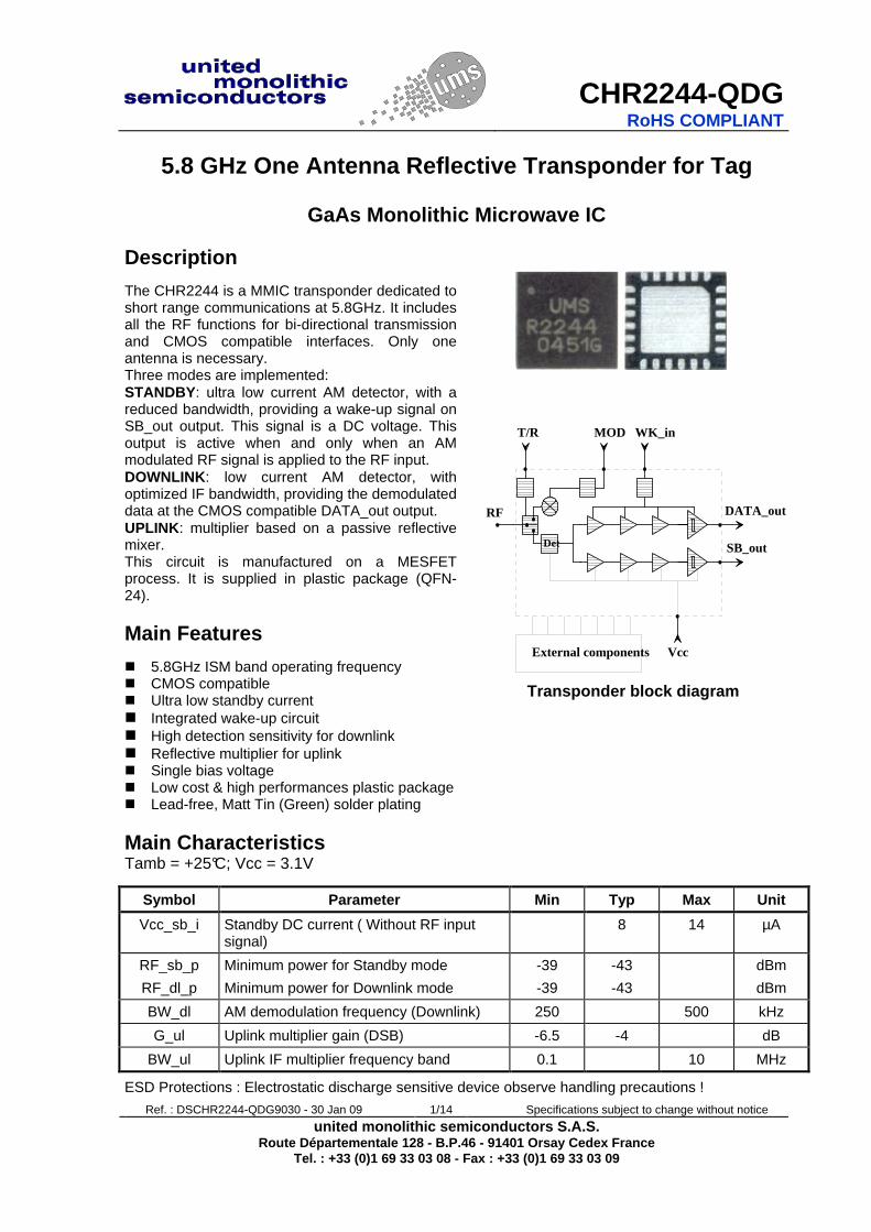
GaAs Monolithic Microwave IC Description The CHR2244 is a MMIC transponder dedicated to short range communications at 5.8GHz. It includes all the RF functions for bi-directional transmission and CMOS compatible interfaces. Only one antenna is necessary. Three modes are implemented: STANDBY : ultra low current AM detector, with a reduced bandwidth, providing a wake-up signal on SB_out output. This signal is a DC voltage. This output is active when and only when an AM modulated RF signal is applied to the RF input. DOWNLINK : low current AM detector, with optimized IF bandwidth, providing the demodulated data at the CMOS compatible DATA_out output. UPLINK : multiplier based on a passive reflective mixer. This circuit is manufactured on a MESFET process. It is supplied in plastic package (QFN-24).
Main Features 5.8GHz ISM band operating frequency CMOS compatible Ultra low standby current Integrated wake-up circuit High detection sensitivity for downlink Reflective multiplier for uplink Single bias voltage Low cost & high performances plastic package Lead-free, Matt Tin (Green) solder plating
Det
T/R MOD WK_in
DATA_outRF
External components Vcc
SB_out
Transponder block diagram
Main Characteristics Tamb = +25°C; Vcc = 3.1V
Symbol Parameter Min Typ Max Unit
Vcc_sb_i Standby DC current ( Without RF input signal)
8 14 µA
RF_sb_p
RF_dl_p
Minimum power for Standby mode
Minimum power for Downlink mode
-39
-39
-43
-43
dBm
dBm
BW_dl AM demodulation frequency (Downlink) 250 500 kHz
G_ul Uplink multiplier gain (DSB) -6.5 -4 dB
BW_ul Uplink IF multiplier frequency band 0.1 10 MHz
ESD Protections : Electrostatic discharge sensitive device observe handling precautions !

CHR2244-QDG 5.8 GHz One Antenna Reflective Tag
Ref. : DSCHR2244-QDG9030 - 30 Jan 09 2/14 Specifications subject to change without notice
Route Départementale 128 , B.P.46 - 91401 ORSAY Cedex - FRANCE Tel.: +33 (0)1 69 33 03 08 - Fax : +33 (0)1 69 3 3 03 09
Electrical Characteristics (Full operating range) Tamb = -30°C to +80°C
Symbol Parameter Test
Conditions Min Typ Max Unit
Fop Operating RF frequency range (1) 5.725 5.8 5.875 GHz
BW_rf RF bandwidth 50 MHz
RL_rf (*) RF input return loss 50 Ω 12 7 dB
Vcc Bias voltage 2.7 3.1 3.6 V
WK_in_imp (*)
WK_in port impedance 6
10
kΩ
pF
T/R_imp (*) T/R input port impedance 100
10
kΩ
pF
T/R_t (*) Transmit to Receive recovery time 150 µs
R/T_t (*) Receive to Transmit recovery time 50 µs
(1) The centre frequency can be adjusted by a matching network located between the antenna and the RF component. (*) Note: Min & Max values include technological spreads, supply & temperature range effect.
STANDBY mode : T/R_v=0V , MOD_v=0V , WK_in_v=0V
Symbol Parameter Test
Conditions Min Typ Max Unit
SB_out_load Standby output port load impedance
1
10
MΩ
pF
SB_out_v (*)
Standby output port
DC voltage high level (1)
low level
Vcc-1
0
Vcc
1
V
V
RF_sb_bw Amplitude modulation frequency of RF for wake-up
250 500 kHz
RF_sb_p (*) Amplitude modulated RF input power for wake-up
(2) -38 -43 dBm
Vcc_sb_i (*) Standby DC current (3) 8 20 µA
(1) The SB_out voltage is high when the RF input signal is AM modulated. (2) Total transmitted power of the modulated signal (modulation index = 0.5) (3) Without RF input signal (*) Note: Min & Max values include technological spreads, supply & temperature range effect.

5.8 GHz One Antenna Reflective Tag CHR2244-QDG
Ref. :DSCHR2244-QDG9030 - 30 Jan 09 3/14 Specifications subject to change without notice
Route Départementale 128 , B.P.46 - 91401 ORSAY Cedex - FRANCE Tel.: +33 (0)1 69 33 03 08 - Fax : +33 (0)1 69 3 3 03 09
DOWNLINK mode : T/R_v=0V , MOD_v=0V , WK_in_v=‘Vcc’
Symbol Parameter Test
Conditions Min Typ Max Unit
Data_out_load Downlink output port
load impedance
CMOS compatible
Data_out_f Amplitude demodulation frequency 250 500 kHz
Data_out_dc (*)
Data_out signal duty cycle 40 50 60 %
RF_dl_p (*) Amplitude modulated RF input power
(1) -38 -43 dBm
WK_in_i (*) WK_in DC current 200 500 µA
(1) Total transmitted power of the modulated signal (modulation index = 0.5) (*) Note: Min & Max values include technological spreads, supply & temperature range effect.
UPLINK mode : T/R_v =‘Vcc’ , WK_in_v =‘Vcc’
Symbol Parameter Test
Conditions Min Typ Max Unit
MOD_imp (*) Modulated signal input port impedance
100
10
kΩ
pF
MOD_v Modulated signal input port voltage
Square wave (1)
0/Vcc
MOD_f Uplink IF multiplier frequency 0.1 10 MHz
G_ul (*) Uplink multiplier gain (DSB) -7 -4 dB
WK_in_i (*) WK_in DC current 200 500 µA
(1) The shape of the modulated signal can be optimized if better linearity is needed. (*) Note: Min & Max values include technological spreads, supply & temperature range effect.
Absolute Maximum Ratings (1) Tamb = -30°C to +80°C
Symbol Parameter Values Unit
Vcc Bias voltage 5 V
Wk_in_v Wk_in input voltage 5 V
T/R_v T/R input voltage 5 V
MOD_v MOD input voltage 5 V
RF_sb_p
RF_dl_p
Maximum Standby and Downlink
RF input power (2)
+10 dBm
Top Operating temperature range -30 to +80 °C
Tstg Storage temperature range -55 to +125 °C
(1) Operation of this device above anyone of these parameters may cause permanent damage. (2) Duration < 1s.
Package outline (1)

CHR2244-QDG 5.8 GHz One Antenna Reflective Tag
Ref. : DSCHR2244-QDG9030 - 30 Jan 09 4/14 Specifications subject to change without notice
Route Départementale 128 , B.P.46 - 91401 ORSAY Cedex - FRANCE Tel.: +33 (0)1 69 33 03 08 - Fax : +33 (0)1 69 3 3 03 09
Pin number
Pin name
Description
4, 5, 6, 8, 9, 10, 16, 18, 23, 24 Non Connected
1 RF RF port
2 T/R Transmit / Receive input port
3 MOD Modulation input port
7 SENS Stand-by sensitivity adjust port
11 Vcc Supply voltage
12 Ga_SB Stand-by amplifiers Gain adjust port
13 SB_out Stand-by output port
14 C4 External decoupling
15 DATA_out Downlink output port
17 WK_in Supply voltage input port for wake-up
19 AD Wake-up threshold adjust port
20 Ga_WK Wake-up amplifiers Gain adjust port (optional)
21 CG External decoupling
22 FD External decoupling
25 slug GND Ground
(1)The package outline drawing included to this data-sheet is given for indication. Refer to the application note AN0017 available at http://www.ums-gaas.com for exact package dimensions.
External Components
5.8 GHz One Antenna Reflective Tag CHR2244-QDG
Ref. :DSCHR2244-QDG9030 - 30 Jan 09 5/14 Specifications subject to change without notice
Route Départementale 128 , B.P.46 - 91401 ORSAY Cedex - FRANCE Tel.: +33 (0)1 69 33 03 08 - Fax : +33 (0)1 69 3 3 03 09
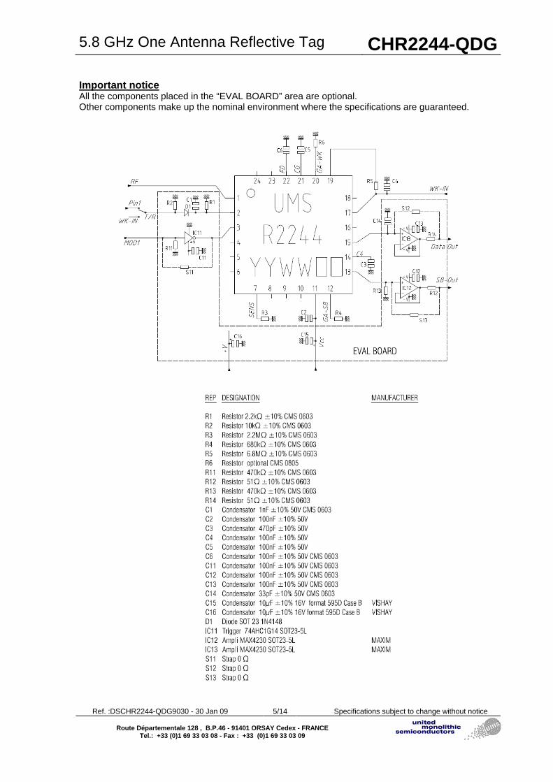
Important notice All the components placed in the “EVAL BOARD” area are optional. Other components make up the nominal environment where the specifications are guaranteed.

CHR2244-QDG 5.8 GHz One Antenna Reflective Tag
Ref. : DSCHR2244-QDG9030 - 30 Jan 09 6/14 Specifications subject to change without notice
Route Départementale 128 , B.P.46 - 91401 ORSAY Cedex - FRANCE Tel.: +33 (0)1 69 33 03 08 - Fax : +33 (0)1 69 3 3 03 09
Design Recommendations All of the different inputs (TR, Mod) and outputs (SB_out, DATA_out) should be properly isolated
(separated enough or with a ground path between them). As T/R port is the most sensitive one, a specific circuit (see on diagram) can be used for high level
of isolation.
Device slug should be connected to RF ground plane through multiples vias (>=9). An external matching may be required to optimize RF performances on 50Ω impedance, versus
substrate height. A RF ground plane height of 0.008” (0.203mm) under the component (evaluation board) provides the highest RF performances thanks to low RF ground inductance and low pin to pin coupling.
Adjustment abilities
Pin number Pin name Component Description
7 SENS R3
Standby sensitivity adjust port :
A value lower than 2.2MΩ decreases Standby chain sensitivity.
12 Ga_SB R4
Standby amplifiers Gain adjust port :
A value lower than 680kΩ increases Standby chain sensitivity.
19 AD R5
Downlink threshold adjust port :
A value lower than 6.8MΩ decreases Downlink chain sensitivity.
20 Ga_WK R6
Downlink amplifiers Gain adjust port :
A value lower than 220 kΩ increases Downlink chain sensitivity.
IMPORTANT NOTICE : All this adjustments may cause non linear response of the performances versus resistors values. The sensitivity is –1x(Minimum RF power for considered mode). Indeed, a decrease of the sensitivity means an increase of the minimum RF power for considered mode.

5.8 GHz One Antenna Reflective Tag CHR2244-QDG
Ref. :DSCHR2244-QDG9030 - 30 Jan 09 7/14 Specifications subject to change without notice
Route Départementale 128 , B.P.46 - 91401 ORSAY Cedex - FRANCE Tel.: +33 (0)1 69 33 03 08 - Fax : +33 (0)1 69 3 3 03 09
Adjustment abilities characterization Typical performance, Tamb = +25°C, Vcc = 3.1V STANDBY sensitivity
The maximum value of R3 resistor is 2.2MΩ. It could be used in order to reduce the Standby sensitivity. The R4 resistor should be used to set the Standby sensitivity higher or lower. The following table gives the typical relation between R3, R4 and the Standby sensitivity.
R3 (MΩΩΩΩ) R4 (kΩΩΩΩ) Sensitivity (dB)
>2.2 indifferently Non guaranteed functionality 2.2 100 S + 1.5 dB 2.2 220 S + 1 dB 2.2 390 S + 0.5 dB
2.2 (*) 680 (*) S (*) 2.2 1200 S - 0.5 dB 2.2 3300 S - 1.5 dB 2.2 6800 S - 3 dB 2.2 No Resistor S - 4 dB 1.5 No Resistor S - 5 dB
(*) S is the sensitivity of a given chip in the recommended environment.
In the full operating range and the recommended environment, -|S| < -38 dBm in accordance with the electrical characteristics.
DOWNLINK sensitivity
R5 could be used in order to reduce the Downlink sensitivity or to set the compromise between sensitivity and unwanted data, when no RF signal, due to noise or parasitic coupling. The R6 resistor should be used to set the Downlink sensitivity higher or lower. The following table gives the typical relation between R5, R6 and the Downlink sensitivity.
R5 (MΩΩΩΩ) R6 (kΩΩΩΩ) Sensitivity (dB)
No Resistor 10 S + 2 dB No Resistor 47 S + 1.5 dB No Resistor 220 S + 1 dB No Resistor No Resistor S + 0.5 dB
6.8 (*) No Resistor (*) S (*) (1) 4.7 No Resistor S - 1 dB 3.3 No Resistor S - 2 dB 2.2 No Resistor S - 3 dB 1.5 No Resistor S - 4 dB 1 No Resistor S - 5 dB
(*) S is the sensitivity of a given chip in the recommended environment.
In the full operating range and the recommended environment, -|S| < -38 dBm in accordance with the electrical characteristics.
(1) A higher sensitivity than in recommended configuration may cause significant density of unwanted
data when RF is not modulated. These data are random because of the component noise floor proximity, or can be sensitive to an environment perturbation.

CHR2244-QDG 5.8 GHz One Antenna Reflective Tag
Ref. : DSCHR2244-QDG9030 - 30 Jan 09 8/14 Specifications subject to change without notice
Route Départementale 128 , B.P.46 - 91401 ORSAY Cedex - FRANCE Tel.: +33 (0)1 69 33 03 08 - Fax : +33 (0)1 69 3 3 03 09
Frequency response characterization Typical performance, Tamb = +25°C, Vcc = 3.1V, Recommended envi ronment STANDBY sensitivity versus AM frequency :
-12
-10,5
-9
-7,5
-6
-4,5
-3
-1,5
0
10 100 1000 10000
AM Frequency (kHz)
Sen
sitiv
ity (
dBre
l)
DOWNLINK sensitivity versus AM frequency :
-12
-10,5
-9
-7,5
-6
-4,5
-3
-1,5
0
10 100 1000 10000
AM Frequency (kHz)
Sen
sitiv
ity (
dBre
l)

5.8 GHz One Antenna Reflective Tag CHR2244-QDG
Ref. :DSCHR2244-QDG9030 - 30 Jan 09 9/14 Specifications subject to change without notice
Route Départementale 128 , B.P.46 - 91401 ORSAY Cedex - FRANCE Tel.: +33 (0)1 69 33 03 08 - Fax : +33 (0)1 69 3 3 03 09
Evaluation board Important notice / design recommendations Device slug should be connected to RF ground plane through multiples vias (>=9). An external matching may be required to optimize RF performances on 50Ω impedance, versus substrate height. A RF ground plane height of 0.008” (0.203mm) under the component (evaluation board) provides the highest RF performances thanks to low RF ground inductance and low pin to pin coupling.

CHR2244-QDG 5.8 GHz One Antenna Reflective Tag
Ref. : DSCHR2244-QDG9030 - 30 Jan 09 10/14 Specifications subject to change without notice
Route Départementale 128 , B.P.46 - 91401 ORSAY Cedex - FRANCE Tel.: +33 (0)1 69 33 03 08 - Fax : +33 (0)1 69 3 3 03 09
Application Information General Transmission system The transmission system is described as following, the tag doesn’t generate any frequency:
FoF-AM
TRANSMITMODE
RECEIVEMODE
RECEIVEMODE
TRANSMITMODEFo
Fm
Fo
BEACON
TAG
DOWNLINK
figure 1a
UPLINK
figure 1b
BEACON
TAG
Figure 1: Transmission system operating principle
Two modes of communication are implemented From beacon to tag (figure 1a): the beacon is in transmit mode while the tag is in the receive mode. The beacon sends an Amplitude Modulated (AM) RF signal to the tag. In figure 1a, F-AM is the amplitude modulation frequency and F0 is the carrier. From tag to beacon (figure 1b): the beacon is in receive mode while the tag is in transmit mode. The beacon sends a continuous wave (CW) RF signal to the tag, this signal is then mixed (at tag level) with the MOD input signal (Fm) thanks to a reflective mixer. The reflected signal is sent back to the beacon and is demodulated thanks to an homodyne receiver.

5.8 GHz One Antenna Reflective Tag CHR2244-QDG
Ref. :DSCHR2244-QDG9030 - 30 Jan 09 11/14 Specifications subject to change without notice
Route Départementale 128 , B.P.46 - 91401 ORSAY Cedex - FRANCE Tel.: +33 (0)1 69 33 03 08 - Fax : +33 (0)1 69 3 3 03 09
Tag operating modes Within this transmission system, the CHR2244 operates in three basic modes depending on the WK_in and T/R input signal levels. They are described hereafter:
1 - The STANDBY MODE (figures 2a; 2B and 2c) is a very low power consumption state. In this mode an Amplitude Modulated RF signal is necessary to produce a DC voltage at the SB_out output which may be used to wake-up the CHR2244 by applying Vcc to the WK_in input.
Figure 2a: Standby mode
The received AM modulated RF spectrum is the following (figure 2b), versus the modulation index (m). This plot is done for the minimum AM modulated RF input power ( -40 dBm ) and only for an ideal spectrum with only 2 rows ( 5.7995 and 5.8005 GHz ) i.e. the 5.8 GHz carrier AM modulated with a 500 kHz signal.
7dB9dB12dB
5.8005GHz5.7995GHz
5.8GHz
m=0.5
5.8GHz 5.8GHz
-40dBm
m=0.7 m=0.9
5.8005GHz5.7995GHz 5.8005GHz5.7995GHz
Figure 2b: AM modulated RF spectrum
IF 500kHz
RF 5,8GHz
MODULATOR ATTENUATOR
CHR2244 +V
OSCILLOSCOPE
SB_OUT
Figure 2c: Standby test bench diagram
De
T/R 0V or HI
MOD 0V or HI
WK_in 0V or HI
DATA_out
RF in AM
modulated SB_out to controller
Data from controller
RF-in AM
modulate
T/R0V
WK_in 0V
SB_out
Vcc

CHR2244-QDG 5.8 GHz One Antenna Reflective Tag
Ref. : DSCHR2244-QDG9030 - 30 Jan 09 12/14 Specifications subject to change without notice
Route Départementale 128 , B.P.46 - 91401 ORSAY Cedex - FRANCE Tel.: +33 (0)1 69 33 03 08 - Fax : +33 (0)1 69 3 3 03 09
2 - When the WK_in is set to Vcc (TR remaining at 0V), the CHR2244 switches to the DOWNLINK MODE (figure 3a), allowing an optimized bandwidth for the demodulation. The received data is demodulated and accessible at the DATA_out output.
Figure 3a: Downlink mode
The received AM modulated RF spectrum is as in standby mode.
IF 500kHz
RF 5,8GHz
MODULATOR ATTENUATOR
CHR2244 +V +WK_in
OSCILLOSCOPE
DAT A_OUT
SB_OUT
Figure 3b: Downlink test bench diagram
Vcc
De
T/R0V
MOD 0V
WK_in Vcc
DATA_out to controller
RF in AM
modulated
SB_out
Data from controller
T/ 0V
WK_in 3V
DATA_out
RF-in AM
modulate

5.8 GHz One Antenna Reflective Tag CHR2244-QDG
Ref. :DSCHR2244-QDG9030 - 30 Jan 09 13/14 Specifications subject to change without notice
Route Départementale 128 , B.P.46 - 91401 ORSAY Cedex - FRANCE Tel.: +33 (0)1 69 33 03 08 - Fax : +33 (0)1 69 3 3 03 09
3 - In the UPLINK MODE (figure 4a), the received CW carrier (F0) is multiplied with the modulation signal (Fm) coming from MOD input. In fact, if ETSI CEN TC278 recommendation is applied, the modulation is around the sub-carrier Fm. The resulting reflected signal is a transposition of Fm around the carrier F0 (F0 ± Fm) .
Figure 4a: Uplink mode
RF 5,8GHz
ATTENUATOR
SPEC TRUM ANALYSER
CHR2244 +V T/R
MOD
IF 500kHz
WK_in
Figure 4b: Uplink test bench diagram
De
T/R Vc
modulated 2MHz sub- carrie
WK_i Vc
DATA_ou
Vcc
SB_out
RF 5.8GHz
C
Data from controller
RF product of
5.8GHz X
modulated sub-carrier
RF-
T/ 3
WK_in 3
RF_outSpectru
modulated sub-carrier around carrier
CARRIER

CHR2244-QDG 5.8 GHz One Antenna Reflective Tag
Ref. : DSCHR2244-QDG9030 - 30 Jan 09 14/14 Specifications subject to change without notice
Route Départementale 128 , B.P.46 - 91401 ORSAY Cedex - FRANCE Tel.: +33 (0)1 69 33 03 08 - Fax : +33 (0)1 69 3 3 03 09
4 - I/O configuration summary
T/R WK_in RF_in SB_out DATA_out MOD
Standby 0V or High impedance
0V or High impedance
AM signal >Vcc-1V
CW or no signal <1V
Downlink 0V Vcc CMOS
Uplink Vcc Vcc Input : CW
Output : Fm around the carrier
Modulation signal
(Fm)
AM: Amplitude Modulated CW: Continuous Wave
Ordering Information QFN 4x4 RoHS compliant package : CHR2244-QDG/XY Stick: XY = 20 Tape & reel: XY = 21 Information furnished is believed to be accurate and reliable. However United Monolithic Semiconductors S.A.S. assumes no responsibility for the consequences of use of such information nor for any infringement of patents or other rights of third parties which may result from its use. No license is granted by implication or otherwise under any patent or patent rights of United Monolithic Semiconductors S.A.S. . Specifications mentioned in this publication are subject to change without notice. This publication supersedes and replaces all information previously supplied. United Monolithic Semiconductors S.A.S. products are not authorized for use as critical components in life support devices or systems without express written approval from United Monolithic Semiconductors S.A.S.