Embed Size (px)
Citation preview

Christof WöllInstitute of Functional Interfaces (IFG)Karlsruhe Institute of Technology, KIT
Organics at surfaces, self-assembly
Karlsruhe Institute of Technology, KIT
Institute of Functional Interfaces, IFG
Christof Wöll
Gold-Substrat
Organic Semiconductors making their way to applications
„Chips on a chips bag“
Fabrication using printing technology
S OrganicsInsulator
G
D
„cheap electronics“Organic Field-Effect
Transistor
Siemens (2003)
- PolymersOligomers with high solubility
( “amorphous” OFET‘s)
- RFID-tags
- limited charge carrier mobility causes low frequencies
www.ofet.de

Organic Semiconductors: Charge Carrier Mobilities
Polymers
Molecules, Oligomers
a-Si
Pentacene-OFET
Rubrene-OFET
poly-Si krist.-Si
OFETBottom-Gate-Geometry
Nelson, Lin, Gundlach, Jackson,
APL 72, 1854 (1998)
Rogers and cowork.Sundar et al., Science 303
1644 (2004)
DS
org. HL
Charge Carrier Mobility [cm /Vs] 210-3 10-2 10-1 100 101 102 103
Oligomers:- highly ordered, single crystals - high purity- main interest polycyclic aromatic hydrocarbons (Polyacenes, Benzoids)
For “smart tag” Applications: > 1 cm2/Vs
GVSG
VSD
Insulator

Organic Conductors: Conduction mechanism and influence of impurities
N. Karl, in:Organic Electronic
MaterialsFarchioni & Grosso (Eds)
Anthracene
RT
Farchioni & Grosso (Eds) Springer,
Material Science 41 (2001)
Clear evidence for band-like transport,at higher temperatures hopping transport
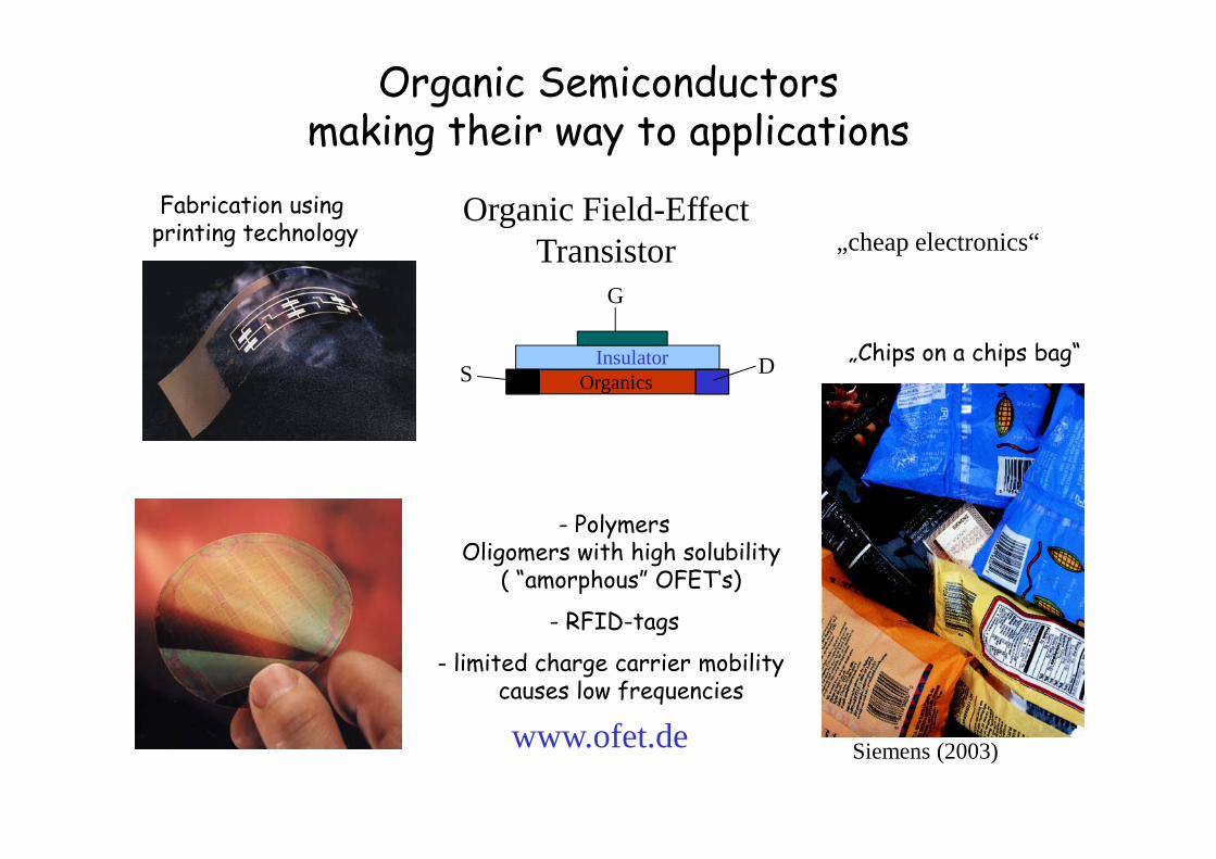
Electronic structure: Conventional vs. organic semiconductors
eV]
Si
Pentacene6.14
Å
a
(1)
(2)
a+ba-b
b
c16.03 Å
7.93 Å
(145 meV)(59 meV)
Ener
gy[e
0.06
GaAs
(260 meV)
R. G. Endres, C. Y. Fong, L. H. Yang, G. Witte, and Ch. W.Comp. Mat. Sci., 29, 362, (2004)
(75 meV)
Precise ab-initio DFT electronic structure calculations

Nucleation & growth on bottom contact OFET-structuresco-operation with Prof. Kunze, Chair for Nano-Electronics, RUB, Bochum
nucleationat
electrodes
9nm pentacene @50oC
Au
SiO2
SiO2
Au
enhanced diffusion
30nm pentacene @90oC
SiO2
50nm pentacene @ 50oC
dewetting at electrodesC.Bock D.V.Pham, U.Kunze, D.Käfer, G.Witte, CW
J. Appl. Phys. 100, 114517 (2006)

It is rather difficult to measure charge carrier mobilities
in organic semiconductors
Would be good to have a modelWould be good to have a model „ideal device“
Metal
Metal
OSC

Fabrication of an „ideal“ OSC-device
Use organic molecular beam deposition, or OMBD,
in ultrahigh vacuum (UHV)
Substrate
Anisotropy !

Molecule (Benzene)
Fabrication of organic surfaces by adsorption of organic molecules on a metal substrate
Gas phase
9
Substrate (Metal)
H.Ohtani, R.J.Wilson, S.Chiang and C.M. Mate,
Phys.Rev.Lett. 60, 2398 (1988)
Rh(111)

NEXAFS for benzene adsorbed on metal surfaces
12
14
16
18
20
22
*
*Benzene multilayer
Au(111)
ofed
geju
mp]
*
Benzene physisorbed
30°
90°
10Weiss, Gebert, Wühn, Wadepohl, WöllJVST A 16, 1017-1022, (1998)
280 285 290 295 300 305 310 315 3200
2
4
6
8
10Rh(111)
Pt(111)
Benzene chemisorbed
Photon Energy [eV]
PEY
[uni
tso
~20°
~30°
Benzene physisorbed
Strong broadening of *-resonance-> chemical interaction
Reduced dichroism of *-resonance-> aplanar distortion

Organic molecular beam deposition of rubrene
OMBD on Au(111) & SiO2
- at RT: only amorphous films
- at 100 oC: dendritc growth 5 µm
- higher substrate temperatures:very rough dendritic islands
then dewetting & desorption
(Tsub~150 oC)
What is so peculiar about rubrene ?

Near Edge X-ray absorption fine structure, NEXAFS
Spectroscopy of unoccupied valence states using synchrotron radiation
Phot
on E
nerg
y
IP
Unoccupiedmolecular orbitals
Absorption
Synchrotron radiationBESSY II, Berlin

OMBD of Rubrene on Au and SiO2C1s NEXAFS:
Multilagen
Additional *-resonanceNo contaminations
Au SiO2
D.Käfer, L.Ruppel, G.Witte and CW, Phys. Rev. Lett. 95, 166602 (2005)

Rubrene: the importance of molecular conformations

OMBD of Rubrene on Au and SiO2C1s NEXAFS:Multilagen
E=210 meV
bulk
Initial growth: twisted gas-phase conformation
Layer thickness >12nm: Nano-crystals, no twist
Twisted conformation: additional *-resonance
Au SiO2
D. Käfer, L. Ruppel, G. Witte and CW, Phys. Rev. Lett. 95, 166602 (2005)

Fabrication of an „ideal“ OSC-device
Rubrene is not the right molecule for OMBD !

Molecules on metals: what is hard and what is soft ?The case of perylene adsorbed on Cu(110)
[10]
1
5 nm
a b9.0Å
00 2020 4040 6060 80 80length [Å]length [Å]
5 nm
0
1
heig
ht [Å
]
heig
ht [Å
]-1
0
1c
III
[1 0]1 [001]
6.4Å
Perylene

Perylene on Cu(110) - Adsorbate-induced reconstruction
9.0Å
6.4Å
Perylene
hw
(5x5)
40 50 60 70 80length [Å]l
dh /
dl
I
II
l 0 1 2 3 4lateral shift
events
[Å]lMolecules
embossing a pattern into a
metal
( )

Perylene on Cu(110) – roughening at higher temperatures
9.0Å
Å
[10]1
[00
cIII
6
3
0
heig
ht [Å
]
a
6.4ÅPerylene
Annealing leads to faceting
d
[001] 0 20 40 60 80 100length [Å]
{551} facet
(5 x 10)
[110
][001]
b
G.Witte, K.Hänel, C.Busse, A.Birkner, CW; Chem. Mater.19, 4228 (2007)

Organic Semiconductors: Charge Carrier Mobilities
Polymers
Molecules, Oligomers
a-Si
Pentacene-OFET
Rubrene-OFET
poly-Si krist.-Si
Nelson, Lin, Gundlach, Jackson,
APL 72, 1854 (1998)
Rogers and cowork.Sundar et al., Science 303
1644 (2004)
Charge Carrier Mobility [cm /Vs] 210-3 10-2 10-1 100 101 102 103
Rubrene: - highly ordered, single crystals - high purity
- not a planar aromatic molecule
For “smart tag” Applications: > 1 cm2/Vs
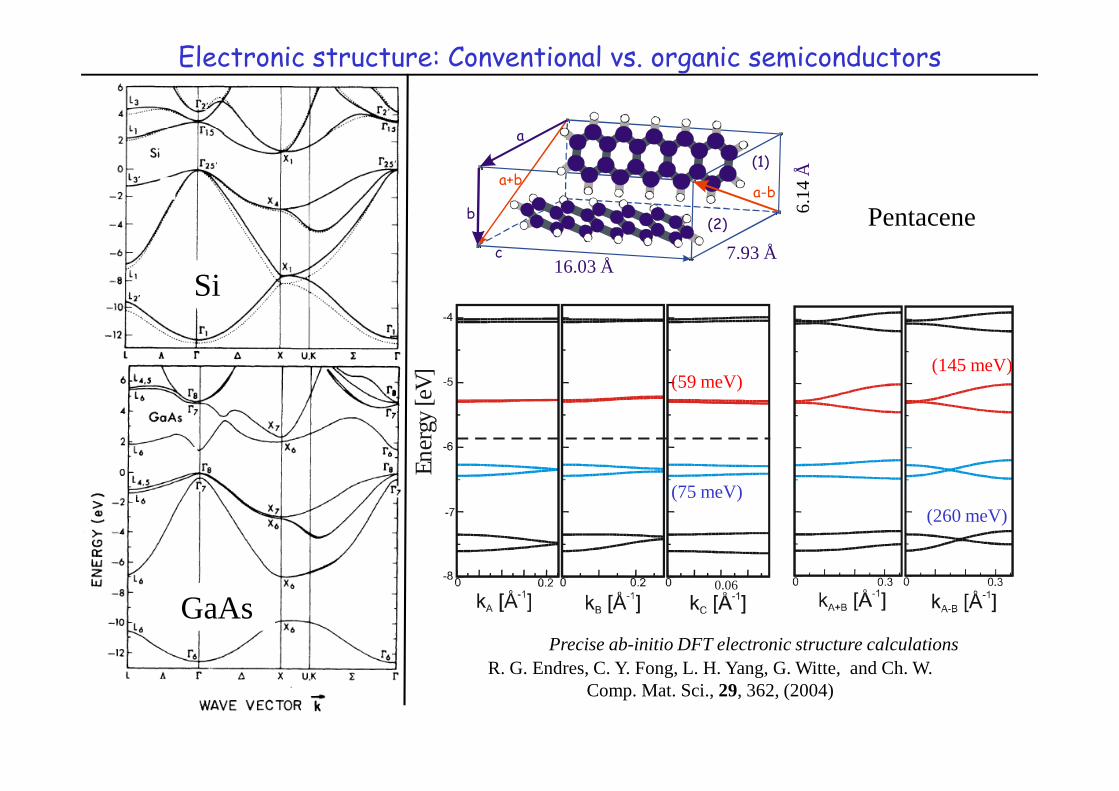
Growth of pentacene on metal substratesGrowth of pentacene on metal substrates
- no -stacking- Bulk structure
- dewetting
Orientational transitions
No OMBE, impossible to grow homogenous, crystalline films on a metal surface
G. Beernink, T. Strunskus,G. Witte, Ch. Wöll Appl. Phys. Lett. 85, 398, (2004)
More detailed studies: rather rule than exception in OMBD of aromatic molecules on metals
Review: Witte & Wöll in : Journal Materials Research, J. Mater. Res. 19, 1889 (2004)

The „ideal“ metal/organic interface: the problems
• Epitaxial growth only for organic molecules which exhibit „orientational precursor“ in bulk(very few, one example is PTCDA)
• Molecular conformation of molecule may be differentMolecular conformation of molecule may be different (rubrene)
• Variation of workfunction (adjustment of electronic level alignment) difficult
Need modification of metal substrate
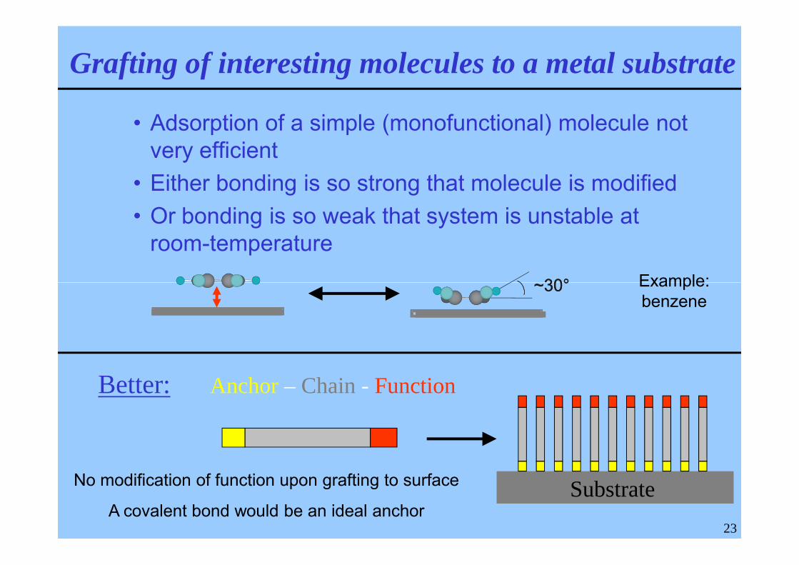
• Adsorption of a simple (monofunctional) molecule not very efficient
• Either bonding is so strong that molecule is modified• Or bonding is so weak that system is unstable at
room-temperature
Grafting of interesting molecules to a metal substrate
30°30° Example:
23
~30°~30°
Better: Anchor – Chain - Function
Substrate
Example: benzene
No modification of function upon grafting to surface
A covalent bond would be an ideal anchor

Most important system today:SAMs made from organothiols
Head group
Anchoring through Au-thiolate bond
24
Anchor
chain,backbone
Octanethiol, alkanethiols
H Gold substrate
R.G. Nuzzo, D.L. Allara, J.Am.Chem.Soc. 105, 4481, (1983)

Most organic molecules are suited for incorporation into organothiols ….
25

Two principal ways to fabricate SAMs …
Deposition in Ultrahigh Vacuum (UHV) Deposition from solution (ambient conditions)
10-10 mBar 1 Bar
26
Very difficult to determine preparation method for SAM after
formation!
All standard methods in
Surface Scienceare applicable !

Diffraction of electrons (LEED):Formation of highly ordered molecular adlayers
27
LEEDDiffraction of low energy electrons(27 eV)
Decane thiolate

Substrate spots
Diffraction of electrons (LEED):Formation of highly ordered molecular adlayers
28
LEEDDiffraction of low energy electrons(27 eV)
Decane thiolate

Decane thiolate
Substrate spots
Superstructure spotsGold substrate
Diffraction of electrons (LEED):Formation of highly ordered molecular adlayers
29
LEEDDiffraction of low energy electrons(27 eV)
(2 3* 3)R30°
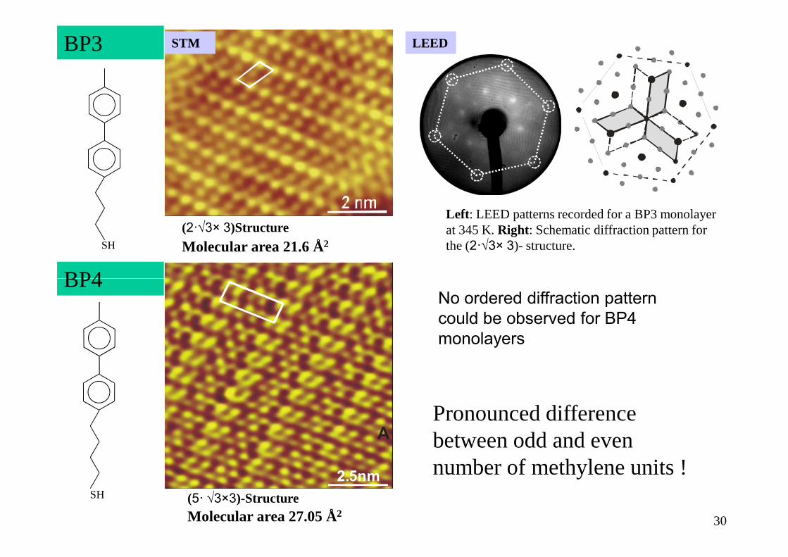
BP3
BP4
STM LEED
(2·3× 3)StructureMolecular area 21.6 Å2
Left: LEED patterns recorded for a BP3 monolayer at 345 K. Right: Schematic diffraction pattern for the (2·3× 3)- structure.SH
30
2.5nm
A
BP4No ordered diffraction pattern could be observed for BP4 monolayers
(5· 3×3)-StructureMolecular area 27.05 Å2
Pronounced difference between odd and even number of methylene units !
SH

Determination of composition and molecular orientation using IR -spectroscopy
0,05
0,10
0,15
0,20
Terphenylthiol Pellet
E
Surface selection rule
Terphenylthiol
KBr pelletIR bulk
31
1000 950 900 850 800 750
0,00
Wavenumbers [cm-1]
-0,0002
0,0000
0,0002
0,0004
0,0006
0,0008
prepared in EtOH solution
1000 950 900 850 800 750
Terphenylthiol/Au(111)
Thiolat-Adlayer on Au
Metal
IRRAS

Analysis of SAM infrared data: Comparison of experiment and theory
S S S S SHarmonic approx.
SH
Summer School on Modern Concepts for Creating and Analyzing
Surfaces and Nanoscale MaterialsSan Feliu, Spain
12. – 16.5.2008
Poor agreementBetween experiment
and theory

Analysis of SAM IRRAS‐data: Comparison of experiment and theory
SH
Katrin Forster‐Tonigold, X. Stammer, CW and A. Groß, submitted for publication
ab initio molecular dynamics simulations

Analysis of SAM IRRAS‐data: Comparison of experiment and theory
Increasingtemperature
SH
temperature
Katrin Forster‐Tonigold, X. Stammer, CW and A. Groß, submitted for publication
ab initio molecular dynamics simulations

Self-assembled monolayers fabricated by immersion of Au-substrates into solutions of organothiols
• SAMs are ultrathin organic films with extremely high structural quality (2D single crystal)
• exhibits organic surfaces mainly defined by -function of thiol
• Basically all traditional techniques form traditional surface science can be applied (including XPS,UPS
35
surface science can be applied (including XPS,UPS and STM)
• Ideal model system for organic molecular beam deposition (?)
Goldkristall
35°

Pentacene / SAM/ Au(111)
Pentacene growth on modified Au(111)-surfaces
Pentacene/Phenylthiol
ab
100 nm
a=6.5 ± 0.4 Åb=7.4 ± 0.4 Å
d=2nm @rt
no morphological changeswithin 72 h
Pentacene/Alkanethiol h=17 ± 3 Å
h
L.Ruppel, A.Birkner, G.Witte, C.Busse, T.Lindner, G.Paasch, CW, J.Appl.Phys. 102, 033708 (2007)
SEM AFM data

Fabrication of an „ideal“ OSC-device
Metal
Metal
OSC
Diode with ohmic contacts
Metal
Metal
Au
Diode with two different tunneling contacts
STM-tip
Au
SAM
Pentacene
Perfect growth on modified substrate !

L l l
Current-Voltage characteristics of „diode“-setup
A total of ~ 50 islands have been investigated
Log. plot onset values at noise level (3·10-4 nA)

Current-Voltage characteristics of „diode“-setup
A total of ~ 50 islands have been investigated
SAM
1 ML
2 ML 3 ML Pentacen
Au(111)
STM
Log. plot onset values at noise level (3·10-4 nA)
• asymmetric onset voltages
• thickness dependent onset voltages for positive sample bias
• onset voltage stays fixed for negative voltage

Conclusions from “model” diode
• n-conduction possible for pentacene, not only p-conduction
• absence of n-conduction evidence for contaminations (e-traps)• Strong evidence for band-like transport in pentacene
(temperature-dep.)• Determination of mobilities should be possible,
numerical simulations underway (difficult)1 ML
2 ML 3 ML Pentacen
STM
Crucial test: Introduce e-trapsOH-groups at organic/metal interface
n-conduction for OSC in the absence of charge traps (-OH at interface)Chua, Zaumseil, Chang, Ou, Ho, Sirringhaus, Friend, Nature 434, 194 (2005).
SAM
1 ML
Au(111)
n-conduction in pentacene ? – absent in most real devices

Idea: Integrate organic semiconductor andinsulator to produce an OFET in a
single-comonent SAM
O i
Au
Organicsemiconductor
Insulatingchain

Long columnar structure
60Ǻ
5Ǻ
SAMs SAMs ofof HBCHBC--CC33 thiolthiol on Au(111on Au(111))
R
RR
R R
S
Christof Wöll, KIT Karlsruhe Organic Electronics: Using SAMs for model devices
Soft tether long range ordered of parallel lamella under the guidance of π-π stacking.
Ut=500 mV, It=100 pA

SAMs SAMs ofof PP--HBC HBC thiolthiol on Au(111) (on Au(111) (measuredmeasured in UHV)in UHV)
Adlayer is transparent
Christof Wöll, KIT Karlsruhe Organic Electronics: Using SAMs for model devicesUt=500 mV, It=100 pA
A
B
A5Å
B30Å
Adlayer is transparentDisk diameter ~ 2.5-3nm

Our results after optimization of preparation conditions:
HBC thiol: preparation conditions matter !
L. Piot, C. Marie, X. Dou, X. Feng, K. Müllen, D. Fichou, JACS 2009, 131, 1378
Christof Wöll, KIT Karlsruhe Organic Electronics: Using SAMs for model devices
Low degree of order, many defects Long-range ordering, low density of defects

NEXAFS for p-HBC-thiolTop view
StructuralStructural model model ofof HBC HBC modifiedmodified thiolthiol
Christof Wöll, KIT Karlsruhe Organic Electronics: Using SAMs for model devices
Side viewCommensurate structure
2 mol./ unit cell

ElectronElectron transporttransport mechanismmechanism ofofHBC SAMs: Information HBC SAMs: Information fromfrom STM ?STM ?
d
STM tip
e-
Apparent height of HBC-islands embedded in insulating matrixdepends on island size
Christof Wöll, KIT Karlsruhe Organic Electronics: Using SAMs for model devices
(e-) transport only along HBC molecule
or(e-) transport also laterally
Au(111)
h
T. Ishida et al., J. Phys. Chem. B. 1999, 103, 1686

Lateral conduction in HBC SAMsLateral conduction in HBC SAMs(insertion of HBC into C10SH(insertion of HBC into C10SH--SAMs)SAMs)
25 min insertion time Apparent island height (h) vs size (d)
α(d +∆h)
Christof Wöll, KIT Karlsruhe Organic Electronics: Using SAMs for model devices
0 10 20 30 40 50-0,2
0,0
0,2
0,4
0,6
0,8
1,0
1,2
Line ALine B
Hei
ght [
nm]
Length [nm]
gap
gap
α(d +∆h)tn HBC gap
α(d +∆h)tn latlat tn gap
HBC HBC
0.5 (R -R - C (d +∆h)e )width =
R R1 1R 1- -R + +1 C (d +∆h)e3 R 3 R
strong evidence for lateral transport
no strong temperature dependence (110K) no hopping transport [~exp(-const/T2)]
Rmol = 13.3/10.4 GΩ (300K),11.6/9.8 GΩ (110K)
Rlat = 2.0/1.5 MΩ (300K),1.7/1.0 MΩ (110K)

An OSC device based on SAMs ?An OSC device based on SAMs ?HBC-thiols form SAMswith long range orderPlane tilted by around 40°
d
Temperature dependence suggeststunneling transport between HBC and Au (Rlat)b d l k ll l h f
Au
Christof Wöll, KIT Karlsruhe Organic Electronics: Using SAMs for model devices
hdband-like transport parallel to the surface
(i.e. within HBC monolayer)Hopping-transport parallel to surface notconsistent with exp. data
Evidence for intrinsic e-mobilities > 5 cm2/Vs

Going tothree dimensions
Christof Wöll, KIT Karlsruhe Organic Electronics: Using SAMs for model devices

Electronic properties of 3‐d NP arrays
MetalInsulator
3d NP‐arrays
EE
C/e2E
spacing
Christof Wöll, KIT Karlsruhe Organic Electronics: Using SAMs for model devices
Metal‐Insulator Transition
D
E = e2/C
Not a metaleven for metal NPs
Single ParticleE ~ EF//N
(3nm Au, 103 atoms,~ 10 meV)
e‐ Charging a capacitor
(~ 0.3 eV)
Exchangecoupling
Markovich, Collier, Henrichs, Remacle, Levine, Heath, Acc Chem Res 32 (1999) 415

2d arrays of metal NPs : Experiment
3d‐arrays
3d NP‐arrays
2d ‐ arrays
Christof Wöll, KIT Karlsruhe Organic Electronics: Using SAMs for model devices
Collier, Saykally, Schiang, Henrichs, Heath Science 277, 1978, (1997)
Needed: Fabrication of 3d‐array with high degree of order (XRD –peaks in all 3 dir.)
Magnetic effects, plasmonics,
Josephson tunneling, Superconductivity,…..
D
10 nm
D = 1…10 nm = 0.5 … 2 nm

Using a 3D shelf system for assembling a 3d NP array
„…it remains a challenge to pattern superlattices with comprehensivecontrol over internal order and overall morphologies…“
W.L. Cheng, N.Y. Park, M.T. Walter, M.R. Hartmann, D. Luo, Nature Nanotechn. 3, 683 (2008)
Ligand shell toavoid sintering
Christof Wöll, KIT Karlsruhe Organic Electronics: Using SAMs for model devices
Problems: How can the shelf be fabricated?How should the loading be carried out?How can electrical contacts be provided?What about using different types of NPs? Non‐spherical?

Loading Au‐clusters into SURMOFs
?
Christof Wöll, KIT Karlsruhe Organic Electronics: Using SAMs for model devices

Objects exhibiting functionality
The goal: surface‐anchored
3d arrays containingadaptable functionalities
Functionality: Static
DynamicSwitchable
The approach: molecular storage racks
Linker+
Connector
The status: SURMOF process
successfully established
AuUltrahinorganic layer
JACS 2007
New process:Liquid phase epitaxy
Switchable
+
Metal‐organic frameworks, MOFs
But:Conventional MOF synthesis not appropriate
Oriented growthCrystallineLoadingElectrical contactsChiral informationPores > 3 nm
Surface‐anchoredMetal‐organic framework
Nat. Mat. 2009
ACIE 2009
JACS 2011
ChemComm2012
Adv.Funct.Mat.2012
Compositional gradient
ACIE 2012
Lateral structuringMOFs are established
Nat.Sci.Rep 2012
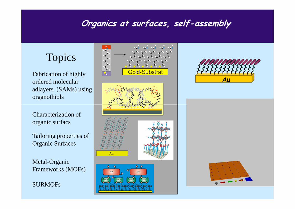
Fabrication of highly ordered molecular adlayers (SAMs) using organothiols
TopicsGold-Substrat
Organics at surfaces, self-assembly
Au
Metal-Organic Frameworks (MOFs)
SURMOFs
Characterization of organic surfacs
Tailoring properties of Organic Surfaces
Au

56

SH
BP3
SAMs from Organothiols with oligopheny-backbone
Systematic studies by
57SH
BP4 varying alkyl chain length
Circular depressions are not defects in film, corrosion of Au-substrate