Embed Size (px)
Citation preview
ACTIVITIES
Characterization of Gallium Antimonide Grown on Semi-Insulating Gallium Arsenide Using Interfacial Misfit Technique
REU Student: Daniel Kim
Graduate Student Mentor: Orlando S. Romero, Nassim Rahimi
Faculty Mentor: Dr. Luke F. Lester, Dr. Sayan D. Mukherjee
A. Introduction
The determination of semiconductor characteristics is an essential part of the process of understanding particular properties of the material. The actual process of characterization can involve different methods depending on the context but consistent to all contexts is the idea that one uses particular methods in order to obtain measurable quantities that relate to the material’s properties. The context here is that of the determination of three characteristic values related to the material being studied, gallium antimonide. The characteristic values are carrier type, carrier concentration, and carrier mobility. Consistently associating the word carrier with all three of these characteristic quantities is not without reason. The word carrier simply refers to the particles that carry charge throughout the material. Though it is worth mentioning that implicit in the word carrier is the idea that these charges are free to move and contribute to a current, which will be elaborated on later. There are two possible charged particles to be considered which are electrons and holes, holes being virtual particles that result from the absence of an electron. Both particles may be referred to synonymously as carriers. The method that is utilized here to obtain the characteristic values mentioned above, and that will be elaborated on in a later portion of this paper, is that of Hall measurements. While the prevalence of material characterization may make Hall measurements made on gallium antimonide seem unexceptional, there are aspects of the characterization of gallium antimonide that make this project particularly deserving of attention. This is especially so when considering the inability to obtain a semi-insulating substrate of gallium antimonide and the reason why this is necessary will be elaborated on and hopefully made clear in the discussion of the method of Hall measurements in the following section. This introduces the added intrigue to an otherwise routine experimental process of studying how the growth technique used to grow the gallium antimonide will affect the characteristic values obtained through Hall measurements.
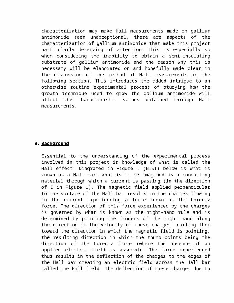
B. Background
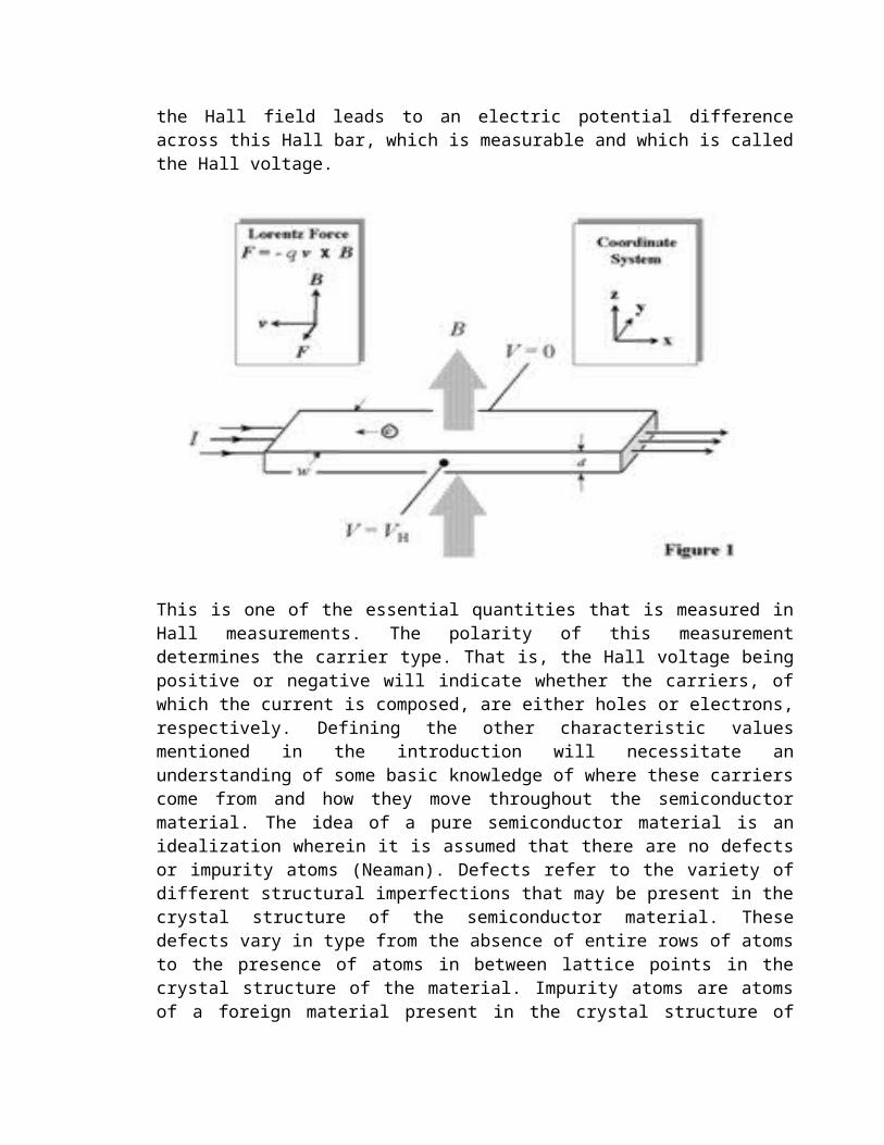
Essential to the understanding of the experimental process involved in this project is knowledge of what is called the Hall effect. Diagramed in Figure 1 (NIST) below is what is known as a Hall bar. What is to be imagined is a conducting material through which a current is passing (in the direction of I in Figure 1). The magnetic field applied perpendicular to the surface of the Hall bar results in the charges flowing in the current experiencing a force known as the Lorentz force. The direction of this force experienced by the charges is governed by what is known as the right-hand rule and is determined by pointing the fingers of the right hand along the direction of the velocity of these charges, curling them toward the direction in which the magnetic field is pointing, the resulting direction in which the thumb points being the direction of the Lorentz force (where the absence of an applied electric field is assumed). The force experienced thus results in the deflection of the charges to the edges of the Hall bar creating an electric field across the Hall bar called the Hall field. The deflection of these charges due to the Hall field leads to an electric potential difference across this Hall bar, which is measurable and which is called the Hall voltage.
This is one of the essential quantities that is measured in Hall measurements. The polarity of this measurement determines the carrier type. That is, the Hall voltage being positive or negative will indicate whether the carriers, of which the current is composed, are either holes or electrons, respectively. Defining the other characteristic values mentioned in the introduction will necessitate an understanding of some basic knowledge of where these carriers come from and how they move throughout the semiconductor material. The idea of a pure semiconductor material is an idealization wherein it is assumed that there are no defects or impurity atoms (Neaman). Defects
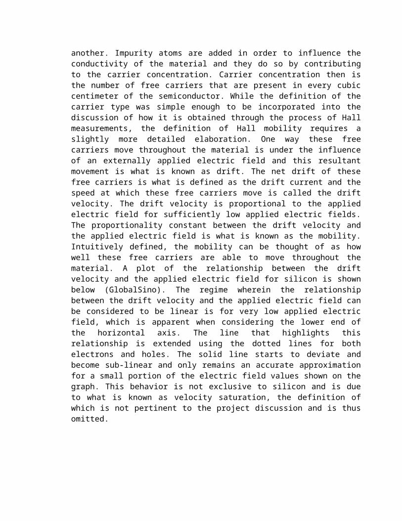
refer to the variety of different structural imperfections that may be present in the crystal structure of the semiconductor material. These defects vary in type from the absence of entire rows of atoms to the presence of atoms in between lattice points in the crystal structure of the material. Impurity atoms are atoms of a foreign material present in the crystal structure of another. Impurity atoms are added in order to influence the conductivity of the material and they do so by contributing to the carrier concentration. Carrier concentration then is the number of free carriers that are present in every cubic centimeter of the semiconductor. While the definition of the carrier type was simple enough to be incorporated into the discussion of how it is obtained through the process of Hall measurements, the definition of Hall mobility requires a slightly more detailed elaboration. One way these free carriers move throughout the material is under the influence of an externally applied electric field and this resultant movement is what is known as drift. The net drift of these free carriers is what is defined as the drift current and the speed at which these free carriers move is called the drift velocity. The drift velocity is proportional to the applied electric field for sufficiently low applied electric fields. The proportionality constant between the drift velocity and the applied electric field is what is known as the mobility. Intuitively defined, the mobility can be thought of as how well these free carriers are able to move throughout the material. A plot of the relationship between the drift velocity and the applied electric field for silicon is shown below (GlobalSino). The regime wherein the relationship between the drift velocity and the applied electric field can be considered to be linear is for very low applied electric field, which is apparent when considering the lower end of the horizontal axis. The line that highlights this relationship is extended using the dotted lines for both electrons and holes. The solid line starts to deviate and become sub-linear and only remains an accurate approximation for a small portion of the electric field values shown on the graph. This behavior is not exclusive to silicon and is due to what is known as velocity saturation, the definition of which is not pertinent to the project discussion and is thus omitted.
The concept of the lattice mismatch between the two materials, that of the substrate GaAs and that of the epitaxial layer under study GaSb, is important to acknowledge. Unit cells are the “small volumes of the crystal that can be used to reproduce the entire crystal” (Neaman, p. 3). The intrinsic crystal structures of the materials under study are comprised of regularly reproduced unit cells in periodic fashion and the space between these unit cells is what is known as the lattice constant (Neaman, p. 3). The lattice constant of GaAs is ~6 Angstrom and of GaSb is ~5.6 Angstrom (Ioffe Institute). This mismatch results in a high concentration of dislocation defects. These dislocation defects can trap carriers thus degrading the characteristic values considered in this project. The growth technique has an effect on this concentration. The growth technique used in this project is that of interfacial misfit (IMF) technique with the growth method being molecular beam epitaxy (MBE). Without this growth technique the dislocation densities, meaning the number of dislocations found per square centimeter, is ~108cm-2 while the density with the IMF technique is ~106cm-2. The method and technique of MBE and IMF will not be explained because the relevant information to be considered is the comparison of the dislocation densities with and without the IMF technique in order to highlight the likelihood of degradation.
C. Research Objective
Objectives as my professor mentor outlined them are as follows (Dr. Luke F. Lester, Center for High Technology Materials, personal communication)
(1) Compare the carrier concentration of n-type (Te-doped) and p-type (Be-doped) GaAs grown on SI-GaAs with n- and p-type GaSb grown with the Interfacial Misfit Dislocation (IMF) technique on SI-GaAs. Orlando Romero will grow these wafers targeting 3 different doping concentrations each for the four sets. There are a total of 12 growths. It is anticipated that these growths will be completed by June 15th.
(2) Learn Hall setup and theory. Measure the samples grown by Orlando in (1). Learn how to interpret Hall data as to its quality and reproducibility.
(3) Assist Orlando in photoluminescence and x-ray diffraction characterization of the structures grown in (1) whenever practical. Observe Molecular Beam Epitaxy (MBE) growth with Orlando.
The primary objective explicitly stated is to obtain the characteristic values of the samples of GaSb grown on SI-GaAs. Acquiring an understanding of Hall setup and theory is essential to this primary objective in that the method utilized to ascertain these characteristic values is that of Hall measurements. An understanding of the relations between the characteristic values and the interfacial misfit (IMF) growth technique is a natural extension outlined in the objectives written by Dr. Luke F. Lester. An assessment of the magnitudes of degradation in the mobility values obtained by Hall measurements of GaSb on SI-GaAs with IMF as compared to GaSb grown on its native substrate will be made possible provided the possibility of making Hall measurements of GaSb when grown on its native substrate. The hypothesized
outcome is that the mobility values will be degraded due to the large concentration of dislocation defects that arise from the mismatch of the lattice constants of GaSb and GaAs.
D. Methodology
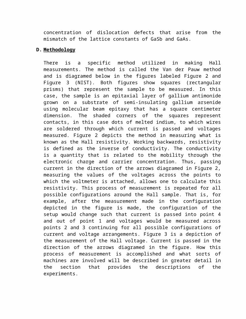
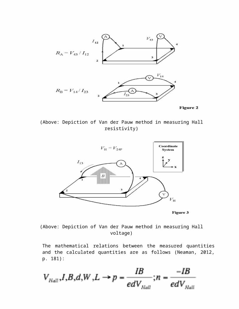
There is a specific method utilized in making Hall measurements. The method is called the Van der Pauw method and is diagramed below in the figures labeled Figure 2 and Figure 3 (NIST). Both figures show squares (rectangular prisms) that represent the sample to be measured. In this case, the sample is an epitaxial layer of gallium antimonide grown on a substrate of semi-insulating gallium arsenide using molecular beam epitaxy that has a square centimeter dimension. The shaded corners of the squares represent contacts, in this case dots of melted indium, to which wires are soldered through which current is passed and voltages measured. Figure 2 depicts the method in measuring what is known as the Hall resistivity. Working backwards, resistivity is defined as the inverse of conductivity. The conductivity is a quantity that is related to the mobility through the electronic charge and carrier concentration. Thus, passing current in the direction of the arrows diagramed in Figure 2, measuring the values of the voltages across the points to which the voltmeter is attached, allows one to calculate this resistivity. This process of measurement is repeated for all possible configurations around the Hall sample. That is, for example, after the measurement made in the configuration depicted in the figure is made, the configuration of the setup would change such that current is passed into point 4 and out of point 1 and voltages would be measured across points 2 and 3 continuing for all possible configurations of current and voltage arrangements. Figure 3 is a depiction of the measurement of the Hall voltage. Current is passed in the direction of the arrows diagramed in the figure. How this process of measurement is accomplished and what sorts of machines are involved will be described in greater detail in the section that provides the descriptions of the experiments.
(Above: Depiction of Van der Pauw method in measuring Hall resistivity)
(Above: Depiction of Van der Pauw method in measuring Hall voltage)
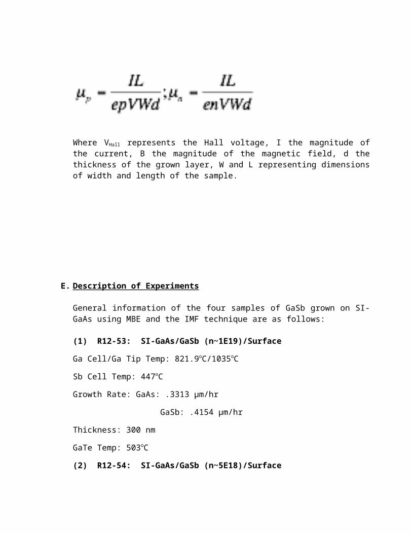
The mathematical relations between the measured quantities and the calculated quantities are as follows (Neaman, 2012, p. 181):
Where VHall represents the Hall voltage, I the magnitude of the current, B the magnitude of the magnetic field, d the thickness of the grown layer, W and L representing dimensions of width and length of the sample.
E. Description of Experiments
General information of the four samples of GaSb grown on SI-GaAs using MBE and the IMF technique are as follows:
(1)R12-53: SI-GaAs/GaSb (n~1E19)/Surface
Ga Cell/Ga Tip Temp: 821.9oC/1035oC
Sb Cell Temp: 447oC
Growth Rate: GaAs: .3313 µm/hr
GaSb: .4154 µm/hr
Thickness: 300 nm
GaTe Temp: 503oC
(2)R12-54: SI-GaAs/GaSb (n~5E18)/Surface
Ga Cell/Ga Tip Temp: 821.9oC/1035oC
Sb Cell Temp: 447oC
Growth Rate: GaAs: .3313 µm/hr
GaSb: .4154 µm/hr
Thickness: 500 nm
GaTe Temp: 484oC
(3)R12-55: SI-GaAs/GaSb (n~1E18)/Surface
Ga Cell/Ga Tip Temp: 821.9oC/1035oC
Sb Cell Temp: 447oC
Growth Rate: GaAs: .3313 µm/hr
GaSb: .4154 µm/hr
Thickness: 1 µm
GaTe Temp: 444oC
(4)R12-56: SI-GaAs/GaSb (n~5E17)/Surface
Ga Cell/Ga Tip Temp: 821.9oC/1035oC
Sb Cell Temp: 445oC
Growth Rate: GaAs: .3313 µm/hr
GaSb: .4154 µm/hr
Thickness: 1 µm
GaTe Temp: 428oC
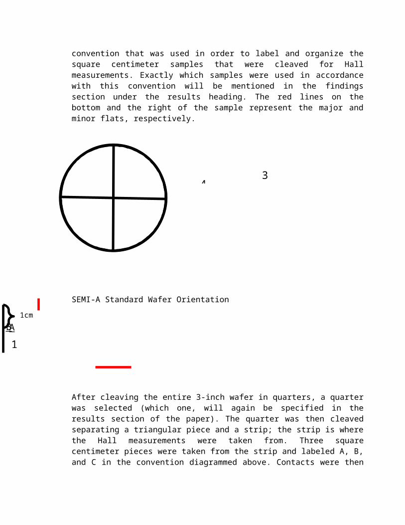
These samples were grown on 3-inch SEMI-A standard wafers. The SEMI-A standard wafers are depicted below along with the convention that was used in order to label and organize the square centimeter samples that were cleaved for Hall measurements. Exactly which samples were used in accordance with this convention will be mentioned in the findings section under the results heading. The red lines on the bottom and the right of the sample represent the major and minor flats, respectively.
SEMI-A Standard Wafer Orientation
3 4
2 1
A
B
C
1cm
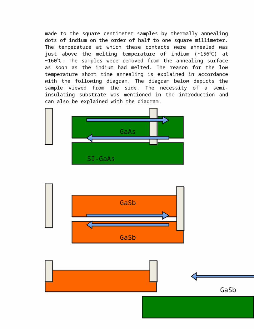
After cleaving the entire 3-inch wafer in quarters, a quarter was selected (which one, will again be specified in the results section of the paper). The quarter was then cleaved separating a triangular piece and a strip; the strip is where the Hall measurements were taken from. Three square centimeter pieces were taken from the strip and labeled A, B, and C in the convention diagrammed above. Contacts were then made to the square centimeter samples by thermally annealing dots of indium on the order of half to one square millimeter. The temperature at which these contacts were annealed was just above the melting temperature of indium (~156oC) at ~160oC. The samples were removed from the annealing surface as soon as the indium had melted. The reason for the low temperature short time annealing is explained in accordance with the following diagram. The diagram below depicts the sample viewed from the side. The necessity of a semi-insulating substrate was mentioned in the introduction and can also be explained with the diagram.
GaAs
SI-GaAs
GaSb
GaSb
SI-GaAs
GaSb
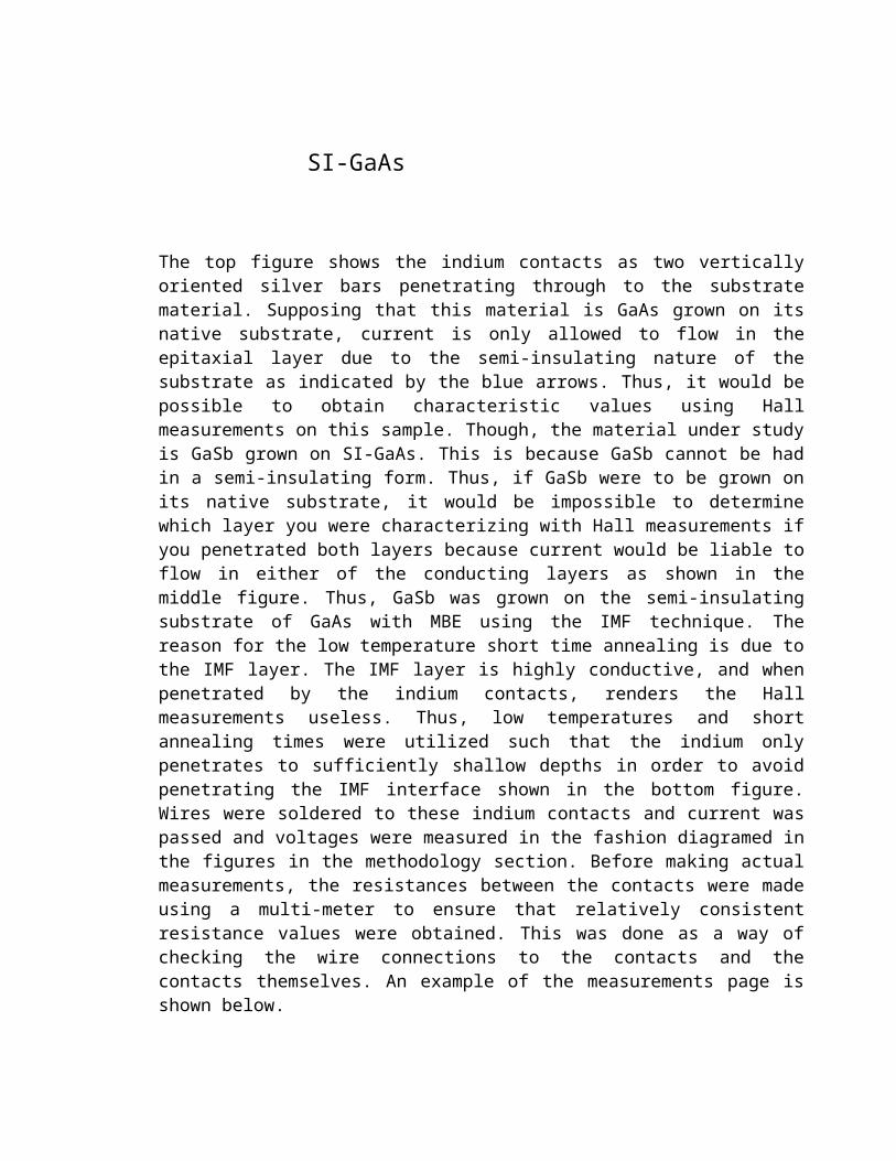
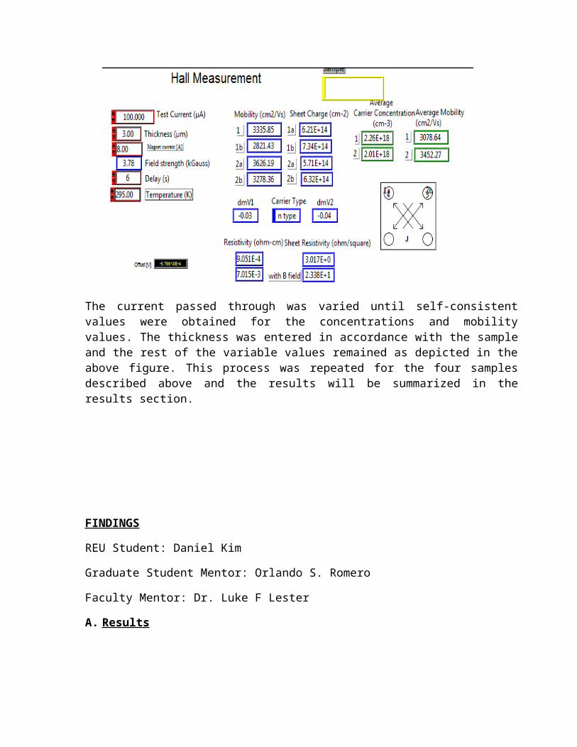
The top figure shows the indium contacts as two vertically oriented silver bars penetrating through to the substrate material. Supposing that this material is GaAs grown on its native substrate, current is only allowed to flow in the epitaxial layer due to the semi-insulating nature of the substrate as indicated by the blue arrows. Thus, it would be possible to obtain characteristic values using Hall measurements on this sample. Though, the material under study is GaSb grown on SI-GaAs. This is because GaSb cannot be had in a semi-insulating form. Thus, if GaSb were to be grown on its native substrate, it would be impossible to determine which layer you were characterizing with Hall measurements if you penetrated both layers because current would be liable to flow in either of the conducting layers as shown in the middle figure. Thus, GaSb was grown on the semi-insulating substrate of GaAs with MBE using the IMF technique. The reason for the low temperature short time annealing is due to the IMF layer. The IMF layer is highly conductive, and when penetrated by the indium contacts, renders the Hall measurements useless. Thus, low temperatures and short annealing times were utilized such that the indium only penetrates to sufficiently shallow depths in order to avoid penetrating the IMF interface shown in the bottom figure. Wires were soldered to these indium contacts and current was passed and voltages were measured in the fashion diagramed in the figures in the methodology section. Before making actual measurements, the resistances between the contacts were made using a multi-meter to ensure that relatively consistent resistance values were obtained. This was done as a way of checking the wire connections to the contacts and the contacts themselves. An example of the measurements page is shown below.
The current passed through was varied until self-consistent values were obtained for the concentrations and mobility values. The thickness was entered in accordance with the
sample and the rest of the variable values remained as depicted in the above figure. This process was repeated for the four samples described above and the results will be summarized in the results section.
FINDINGS
REU Student: Daniel Kim
Graduate Student Mentor: Orlando S. Romero
Faculty Mentor: Dr. Luke F Lester
A. Results
The results for the four samples given in the experimental description section of the activities portion of the paper are summarized in the following table:
Hall Sample
Average Carrier
Concentration (cm-3)
Average Mobility (cm2/V-s)
Resistivity Without
B-Field (-cm)
Sheet Resistivity Without B-
field (/square)
Resistivity With B-Field
(-cm)
Sheet Resistivity
With B-Field
(/square)
Test Current
(A)R12-53 9.69E17 1203.84 5.379E-3 1.793E2 4.777E-3 1.592E2 120.0R12-54 6.95E17 1908.86 4.712E-3 9.423E1 3.982E-3 7.964E1 150.0R12-55 2.16E17 3648.26 7.933E-3 7.933E1 6.010E-3 6.010E1 100.0R12-56 9.25E16 4562.04 1.482E-2 1.482E2 1.301E-2 1.301E2 100.0
Each sample was taken from quarter 1 in the SEMI-A standard. With the exception of sample R12-56, each sample was section A in accordance with the convention diagramed in the experimental description section of the activities portion above. Sample R12-56 was section C in accordance with the same convention. The concentrations are significantly lower from the expected concentrations. Before the low temperature short time annealing methods were used, the values for the concentrations were in the 1020-1021 range, which were even larger than the expected concentration values and even less likely considering the expectation of seeing lower concentrations due to the nature of the material. Current-Voltage (IV) characteristics were taken of the indium contacts made on the sample and resulted in determining the nature of the contacts to be indeed ohmic. It was then though that higher
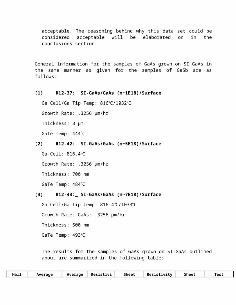
annealing temperatures would help but after a brief discussion of the questionable results it was determined that the unreliable measurements being taken was due to the penetration of the contact through to the IMF layer. The concentrations when compared with the mobility values also appeared counter-intuitive before the low temperature annealing methods were used. After low temperature short time annealing was used, the values given in the table were obtained and were considered to be acceptable. The reasoning behind why this data set could be considered acceptable will be elaborated on in the conclusions section.
General information for the samples of GaAs grown on SI GaAs in the same manner as given for the samples of GaSb are as follows:
(1)R12-37: SI-GaAs/GaAs (n~1E18)/Surface
Ga Cell/Ga Tip Temp: 816oC/1032oC
Growth Rate: .3256 µm/hr
Thickness: 3 µm
GaTe Temp: 444oC
(2)R12-42: SI-GaAs/GaAs (n~5E18)/Surface
Ga Cell: 816.4oC
Growth Rate: .3256 µm/hr
Thickness: 700 nm
GaTe Temp: 484oC
(3)R12-43: SI-GaAs/GaAs (n~7E18)/Surface
Ga Cell/Ga Tip Temp: 816.4oC/1033oC
Growth Rate: GaAs: .3256 µm/hr
Thickness: 500 nm
GaTe Temp: 493oC
The results for the samples of GaAs grown on SI-GaAs outlined about are summarized in the following table:
Hall Average Average Resistivit Sheet Resistivity Sheet Test
Sample
Carrier Concentratio
n (cm-3)Mobility (cm2/V-s)
y Without B-Field (-cm)
Resistivity Without B-
field (/square)
With B-Field (-cm)
Resistivity With B-
Field (/square)
Current (A)
R12-37 2.43E18 2312.42 1.113E-3 3.708 8.649E-4 2.883 3000.0R12-42 3.66E18 2039.00 8.369E-4 1.196E1 6.532E-4 9.332 1000.0R12-43 2.35E18 2280.46 1.164E-3 2.328E1 9.414E-4 1.883E1 500.0
There is an issue with the results for the sample R12-43. As compared to the values measured for R12-37, there is a lower concentration; yet, there is also a lower mobility. With a lower doping concentration one would expect that the mobility values be higher. The reasoning for this will again be elaborated on in the conclusions section, though it should be known that this error was expected. There was a notification of the error during this sample’s growth where the temperature had been raised for an appreciable amount of time (~10 minutes) and lowered back down to the original value (listed in the information as the GaTe temperature). This temperature fluctuation could possibly have had a significant impact on the quality of the growth and consequentially the characteristics of the sample. Thus, there is less reason for the sample R12-43 to be considered as having been measured with success.
B. Conclusions
The objectives of this project were not only to obtain the characteristic values of GaSb epitaxially grown on semi-insulating GaAs but also to understand the affect that the IMF growth technique would have on the mobility values. There are many factors that are not taken into account when making Hall measurements. For example one does not incorporate depletion widths into the calculated values. Thus, many of the characteristic values taken from Hall measurements are considered as averages and thus other methods may be used to obtain more precise measurements of characteristic values like carrier concentration. However, carrier mobility is unambiguous and reliable because the growth process determines the factors taken into account in its calculation. It was expected that the characteristic values of GaSb grown on semi-insulating GaAs would be degraded and that was observed in the results section. The ideal mobility values can be calculated using the following formula (Bett, 2001):
m=mmin+mmax−mmin
1+((ND+N A)/N ref )α
Tables summarizing the measured concentrations and the mobility values and the plot of the carrier concentration versus mobility for both the expected values in
accordance with the formula and the measured values taken from Hall measurements are as follows:
Carrier Concentration (cm-3) Measured Mobility
(cm2/V-s) Ideal Mobility (cm2/V-s)
9.69E+17 1203.84 6590.35
6.95E+17 1908.86 6590.35
2.16E+17 3648.26 6590.35
9.25E+16 4562.04 6590.35
1.00E+16 1.00E+17 1.00E+180
1000
2000
3000
4000
5000
6000
7000
Carrier Concentration vs. Mobility
Mobility (cm2/V-s)Ideal Mobility (cm2/V-s)
Carrier Concentration (cm-3)
Mob
ilit
y (c
m2
/V-s
)
The concentration values of the GaSb were expected to be lower than GaAs because of the intrinsic p-type nature of GaSb that needed to be compensated before becoming n-type. With this data one could determine the amount of p-doping that was being compensated by the n-doping. A sample of un-doped GaSb grown on semi-insulating GaAs using the IMF technique was measured also. On average, the difference in the measured values and the ideal values is approximately 54 percent. The calculation of the compensation could then be compared with this measured value for the un-doped substrate and theoretically they should be comparable to each other. Qualitatively, the outcome of the Hall measurements made on GaSb agrees with our expectations. The natural extension of this agreement would be to determine quantitative relations that

the interfacial misfit growth technique has on the characteristic values of GaSb grown on semi-insulating GaAs.
C. Future Work
Provided evaporated metal contacts can be connected to the Hall set up, it could be possible to take Hall measurements on GaSb samples grown on its native substrate and compare the values with the GaSb grown on the non-native substrate of GaAs. These metal contacts would be shallow enough to ensure that the substrate layer is not penetrated thus only passing current through the epitaxial layer. Diagramed below is a crude depiction of what this would look like.
The shallow contacts would be wired to the Hall set up much in the same way that the samples with the indium contacts were. This would aid in the characterization of GaSb and could contribute to the research of thermal photovoltaic (TPV) generators. (Bett, 2003). This could also contribute to the study of utilizing GaSb in multi-junction solar cell applications (Bett, 2001).
(p- or n-type) GaSb
(n- or p-type) GaSb
References
Neaman, Donald A., 2012, Semiconductor Physics and Devices, McGraw-Hill, New York City, 758 p.
NIST, December 2, 2011, National Institute of Standards and Technology, The Hall Effect, http://www.nist.gov/pml/div683/hall_effect.cfm, July 23, 2012
GlabalSino, October 15, 2011, GlobalSino, Drift Velocity Versus Electric Field in Silicon, http://www.globalsino.com/micro/1/1micro9938.html
Ioffe Institute, 1998-2001, Ioffe Physico-Technical Institute, New Semiconductor Materials. Characteristics and Properties, Gallium Arsenide, http://www.ioffe.ru/SVA/NSM/Semicond/GaAs/basic.html
Ioffe Institute, 1998-2001, Ioffe Physico-Technical Institute, New Semiconductor Materials. Characteristics and Properties, Gallium Antimonide,http://www.ioffe.rssi.ru/SVA/NSM/Semicond/GaSb/basic.html
Bett A. W., Sulima O. V., 2003, GaSb Photovoltaic Cells for Applications in TPV Generators, IOP Science, http://iopscience.iop.org/0268-1242/18/5/307
Bett A. W., Adelhelm R., Agert C., Beckert R., Dimroth F., Shubert U., 2001, Advanced III-V Solar Cell Structures Grown by MOVPE, Solar Energy Materials & Solar Cells
Bett, A. W., Sulima O. V., 2001, Fabrication and Simulation of GaSb Thermophotovoltaic Cells, Solar Energy Materials & Solar Cells 66