Embed Size (px)
Citation preview

CIRCUIT DESIGN FOR AN ION MOBILITY SPECTROMETER
by
Ravindra Puthumbaka
A Project
submitted in partial fulfillment
of the requirements for the degree of
Master of Science in Electrical Engineering,
Boise State University
November, 2004

ii
The project presented by Ravindra Puthumbaka entitled “CIRCUIT DESIGN
FOR AN ION MOBILITY SPECTROMETER” is hereby approved:
Dr. R. Jacob Baker, Advisor Date
Dr. Joe Hartman, Committee Member Date
Dr. Jeff Jessing, Committee Member Date
Dr. John R. Pelton, Graduate Dean Date

iii
ACKNOWLEDGEMENTS
It has been a great honor to do my Masters in EE at Boise State University.
First of all, I would like to thank my advisor, Dr. Jake Baker who has given me quality
education, guidance and motivation. I thank the Environmental Protection Agency (EPA)
for funding the sensor project and providing an opportunity for me for research. I also
thank the Project Investigator, Dr. Joe Hartman and other team members whose
suggestions have helped me complete this project. Last but not the least, I would like to
thank Dr. Jeff Jessing for his valuable suggestions.
I dedicate this work to my family.

iv
TABLE OF CONTENTS
ACKNOWLEDGEMENTS............................................................................................... iii
LIST OF ABBREVATIONS ............................................................................................. vi
LIST OF FIGURES .......................................................................................................... vii
ABSTRACT........................................................................................................................ x
CHAPTER 1: INTRODUCTION....................................................................................... 1
WORKING OF AN IMS................................................................................................. 3
DESIGN REQUIREMENTS .......................................................................................... 6
CHAPTER 2: DESIGN OF POWER SUPPLY ................................................................. 8
CHAPTER 3: DESIGN OF LEVEL TRANSLATOR CIRCUITS .................................. 10
LEVEL TRANSLATOR 1............................................................................................ 10
SPICE SIMULATIONS ............................................................................................. 12
MEASURED RESULTS ............................................................................................ 15
LEVEL TRANSLATOR 2............................................................................................ 17
SPICE SIMULATIONS ............................................................................................. 20
PROTECTION CIRCUITS........................................................................................... 22
CHAPTER 4: DESIGN OF CHARGE PUMP ................................................................. 24
SIMULATION RESULTS: .......................................................................................... 28
CHAPTER 5: BUILDING PC BOARDS & TESTING CIRCUITS................................ 31

v
CHAPTER 6: PERFORMANCE AND RESULTS.......................................................... 35
VARIATION OF LOAD VS INPUT CLOCK FREQUENCY........................................................ 35
OUTPUT VOLTAGE VARIATION WITH NUMBER OF STAGES ............................................ 37
EFFICIENCY ............................................................................................................... 38
CONCLUSION............................................................................................................. 39
FUTURE WORK .............................................................................................................. 39
CHAPTER 7: SENSING CIRCUIT ................................................................................. 40
FIRST ORDER ΔΕ MODULATOR ..................................................................................... 43
CHAPTER 8: SIMPLE NOISE-SHAPING MODULATOR........................................... 49
MODULATION NOISE IN A FIRST ORDER NS MODULATOR ............................................ 51
IDEAL SNR OF A FIRST ORDER NS MODULATOR........................................................... 56
CHAPTER 9: IMPLEMENTATION OF THE SENSING CIRCUIT.............................. 60
CONCLUSION............................................................................................................. 64
APPENDIX: SPICE MODELS AND NETLIST ............................................................. 65
REFERENCES ................................................................................................................. 73

vi
LIST OF ABBREVATIONS
BSU ..................................................................................................Boise State University.
DC ................................................................................................................. Direct Current
DSM ……………………………………………………….........Delta Sigma Modulation.
EPA ...............................................................................Environmental Protection Agency.
IMS ...........................................................................................Ion Mobility Spectrometer.
HRIMS .......................................................... High Resolution Ion Mobility Spectrometer.
LTCC .......................................................................Low Temperature Co Fired Ceramics.
CHEMFET ......................................................................Chemical Field Effect Transistor.
PIC ........................................................................................ Program Interrupt Controller.
MOS ....................................................................................... Metal Oxide Semiconductor.
PMOS .................................................................... P-channel Metal Oxide Semiconductor.
NMOS ...................................................................N-channel Metal Oxide Semiconductor.
PCB ................................................................................................... Printed Circuit Board.
SPICE ............................................ Simulation Program with Integrated Circuit Emphasis.
PSD ………………………………………………………………Power Spectral Density.
AC ............................................................................................................ Alternate current.
ADC …………………………………………………………Analog to Digital Converter.
SNR ……………………………………………………………….. Signal to Noise Ratio.
RMS ………………………………………………………………….. Root Mean Square.
NTF …………………………………………………………….. Noise Transfer Function.
NS ……………………………………………………………………...…. Noise Shaping.

vii
LIST OF FIGURES Figure 1.1: Sensor system overview .................................................................................. 2 Figure 1.2: Block Diagram of the IMS system................................................................... 4 Figure 1.3: Conceptual Drawing of IMS (solid works) ...................................................... 5 Figure 2.1: Block diagram of Power supply scheme .......................................................... 8 Figure 3.1: Schematic of the level translator circuit ......................................................... 10 Figure 3.2: Schematic of the inverters [labeled as U]....................................................... 11 Figure 3.3: Simulation showing PIC signal [top] and the level translator’s output.......... 12 Figure 3.4: Simulation showing the output transition and contention current [in red]..... 13 Figure 3.5: Simulation showing the rise time of the inverter [80ns] ................................ 14 Figure 3.6: Simulation showing the fall time of the inverter [8ns]................................... 14 Figure 3.7: Measured results on the PCB ......................................................................... 15 Figure 3.8: Rise time of the inverter measured on the PCB [90ns] .................................. 16 Figure 3.9: Fall time of the inverter measured on the PCB [20ns] ................................... 16 Figure 3.10: Schematic of circuit used for 12V to 200V conversion ............................... 17 Figure 3.11: Voltage shifts on the gate of the MOSFETs Q1/Q3..................................... 18 Figure 3.12: Combined schematic of the level translators................................................ 19 Figure 3.13: Voltage switching on the gate of the PMOSFET Q1 ................................... 20 Figure 3.14: CLKHV and CLKHVI from simulations. .................................................... 21 Figure 3.15: Expanded schematic view of one phase of the clock ................................... 22 Figure 3.16: Power supply protection circuit.................................................................... 23 Figure 4.1: Schematic of the charge pump. ...................................................................... 24

viii
Figure 4.2: Final simulated output of the power supply circuit [2kV] ............................. 28 Figure 4.3: Feed back signal from the power supply circuit to the PIC ........................... 29 Figure 4.4: Final output of the power supply circuit and 200V clocks............................. 30 Figure 5.1: Printed Circuit Board Layout of the power supply circuit ............................. 31 Figure 5.2: Final prototype of the power supply circuit ................................................... 32 Figure 5.3: Equipment used to test the PCB circuits ........................................................ 33 Figure 6.1: Load resistance versus frequency with 12 stages........................................... 35 Figure 6.2: Load resistance versus frequency with 7 stages............................................. 36 Figure 6.3: Output Voltage vs. Number of Stages in Charge Pump................................. 37 Figure 7.1: Typical output signals from the IMS.............................................................. 40 Figure 7.2: Frequency domain for an oversampling converter......................................... 41 Figure 7.3: Block diagram of an oversampling ADC....................................................... 42 Figure 7.4: Basic first order delta sigma modulator ......................................................... 43 Figure 7.5: Frequency domain model of a first-order delta-sigma modulator.................. 45 Figure 7.6: Frequency response of the first-order delta sigma modulator. ....................... 46 Figure 7.7: RMS quantization noise in a typical ADC with sampling frequency fs ......... 47 Figure 7.8: RMS quantization noise in an oversampled ADC (sampling frequency Kfs) 47 Figure 8.1: Analog implementation of a first order Noise shaping modulator................. 49 Figure 8.2: Spice simulation of a first order NS modulator in figure 40 ......................... 50 Figure 8.3: z-domain representation of the NS modulator ............................................... 51 Figure 8.4: Theoretical Modulation noise for a first order NS modulator........................ 53 Figure 8.5: Slow ramp input to the modulator and its corresponding output ................... 54

ix
Figure 8.6: Modulation noise for a slow ramp input to the modulator ............................. 55 Figure 8.7: PSD of the modulation noise for a slow ramp input to the modulator. .......... 56 Figure 9.1: Schematic of the first order NS modulator implemented............................... 60 Figure 9.2: PCB layout of the Delta Sigma Modulator [size – 1.7”x4”] .......................... 60 Figure 9.3: Measured response of the Delta Sigma Modulator ........................................ 60
Figure 9.4: DC analysis of the Delta Sigma Modulator.................................................... 60

x
ABSTRACT
The Ion Mobility Spectrometer needs a high voltage power supply circuit and a
sensing circuit. The high voltage power supply is used to maintain a uniform potential
difference across the drift tube. A sensing circuit is needed to amplify the output signals
from the Ion Mobility Spectrometer so that they can be read and interpreted by the micro
controller.
The design of the power supply is achieved by using a voltage multiplier circuit and a
level shifting circuit is employed to produce high voltage clock pulses from a low voltage
clock pulse source. Low power consumption, stable response to load resistance and
oscillator frequency changes, and good efficiency are vital characteristics, which
determine the performance of the power supply.
Sensing circuit design needs a low-cost, low-bandwidth, low-power consuming high
resolution Analog to Digital Converter. The design is conceived by using Delta Sigma
modulation techniques. Delta sigma modulation uses simple analog electronics. It’s a
very low cost technique that achieves high resolution by shaping the Quantization noise.

xi
Report Organization The project is divided in to six chapters:
• Chapter one gives an overview of the Sensor Project and a brief description of the
concept of Ion Mobility Spectrometry. The assembly of an IMS is also described.
It also gives the design requirements to be met.
• Chapter two gives an introduction of the design of the power supply circuit.
• Chapter three describes the design of the level translator circuits, simulations in
Hspice and measured results on printed circuit boards.
• Chapter four describes the design of the charge pump circuit, simulations and
measured results.
• Chapter five describes the layout of the printed circuit board and the experimental
results.
• Chapter six describes the performance of the power supply circuit.
• Chapter seven gives an introduction to the sensing circuit needed for the IMS and
the concept of delta sigma modulation
• Chapter eight describes the design of the first order Noise-shaping modulator with
simulations.
• Chapter nine describes the implementation of the first order Noise-shaping
modulator on a Printed Circuit Board using discrete components.

xii
Achievements
• A 2000V, 1.25W, power supply is built on a Printed Circuit Board (PCB) using
discrete components.
• The power supply built was 1.2” x 6” in size.
• Prototype built was tolerant to loads between 20MΩ and 60MΩ with frequency
ranging between 20KHz and 100KHz.
• The prototype was also tolerant to supply voltage variations, with power
efficiency equal to 9%.
• A first-order noise-shaping modulator was built on a PCB using discrete
components and the concept demonstrated.

1
CHAPTER 1: INTRODUCTION
The Multipurpose Sensors project to detect and analyze environmental [subsurface]
contaminants was started in July 2002. The goal is to develop sensors to provide real time
data on the quantity and identity of contaminants like heavy metals and volatile organic
compounds. This involves development of solid-state electrochemical sensors for heavy
metals, and fabrication of a miniaturized High Resolution Ion Mobility Spectrometer.
The whole system has the following components:
a) Ion Mobility Spectrometer,
b) Electrochemical sensors,
c) Control and Sensing circuitry,
d) Embedded microcontroller,
e) Temperature and Pressure Sensors,
f) Wireless transmission subsystem,
g) Optional GPS Subsystem and
h) A host computer with software to accumulate transmitted data from sensors.

2
The system overview would look as shown in figure 1.1.
Cellular Transmission
Figure 1.1: Sensor system overview
Our group was assigned to design the power supply and sensing circuit for the IMS.
The micro controller turns on the power supply to power up the IMS when a cycle of
sensing is started. After 32 cycles of sensing are done, the IMS power supply is turned
off. Each cycle of sensing lasts 20ms. During this period, the IMS outputs signals which
represent the contaminants concentration. The sensing circuit is used to amplify these
signals to levels that can be read by the micro controller.
Ion Mobility Spectrometer
Electrochemical Sensors
Sensing Circuit
Embedded Microcontroller
GPS
Power Supply
Wireless Transmission Sub-system
Sensing Circuit
Central Computer
3
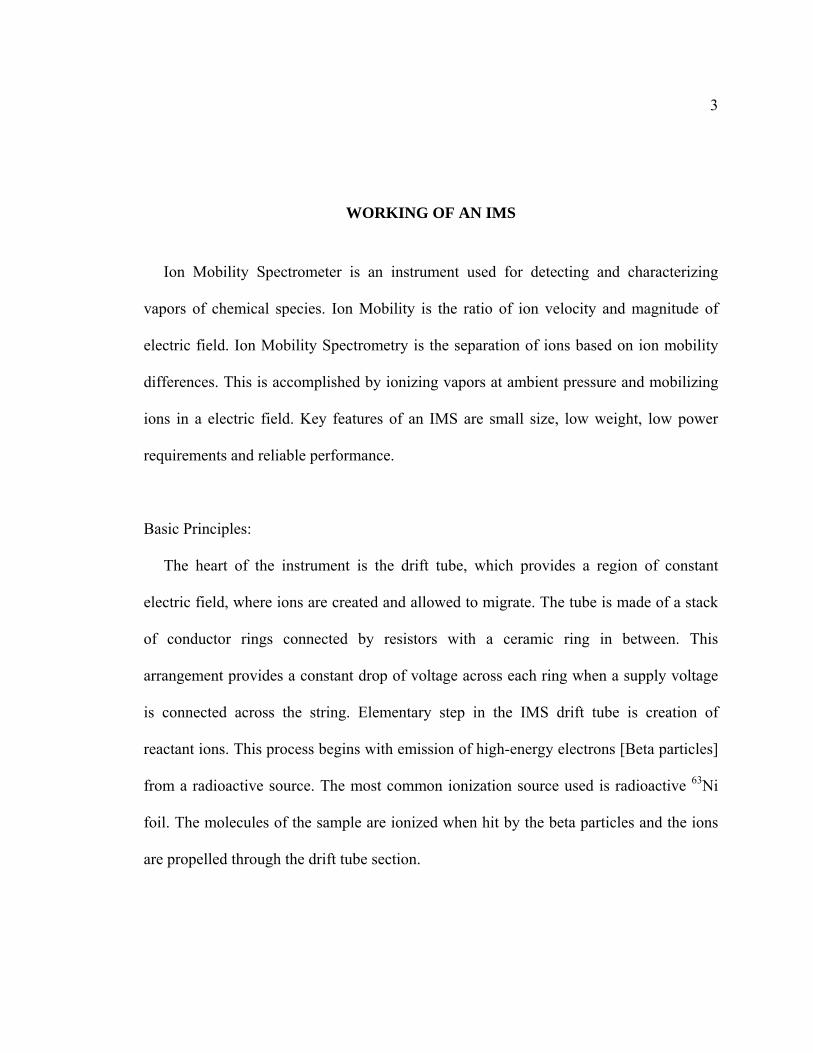
WORKING OF AN IMS
Ion Mobility Spectrometer is an instrument used for detecting and characterizing
vapors of chemical species. Ion Mobility is the ratio of ion velocity and magnitude of
electric field. Ion Mobility Spectrometry is the separation of ions based on ion mobility
differences. This is accomplished by ionizing vapors at ambient pressure and mobilizing
ions in a electric field. Key features of an IMS are small size, low weight, low power
requirements and reliable performance.
Basic Principles:
The heart of the instrument is the drift tube, which provides a region of constant
electric field, where ions are created and allowed to migrate. The tube is made of a stack
of conductor rings connected by resistors with a ceramic ring in between. This
arrangement provides a constant drop of voltage across each ring when a supply voltage
is connected across the string. Elementary step in the IMS drift tube is creation of
reactant ions. This process begins with emission of high-energy electrons [Beta particles]
from a radioactive source. The most common ionization source used is radioactive 63Ni
foil. The molecules of the sample are ionized when hit by the beta particles and the ions
are propelled through the drift tube section.

4
Ions are injected into the drift region as a packet of ions using the shutter grid. This
packet moves under the influence of electric field and the ions attain a velocity according
to their mobility. A steady flow of drift gas is swept through the drift tube to minimize
the secondary effect of buildup of impurities that could otherwise react with ions and
distort mobility spectra.
The Gate [Tyndall gate] is used to control the flow of ions down the drift tube. It used
two parallel rings with a wire mesh normal to the flow of ions. This is controlled by the
micro controller to block or pass ions traveling in drift field. Flow of ions is stopped by
raising the field voltage at the gate above the field voltage in the tube. The gate is pulsed
(around every 20ms) to transport ions. Figure 1.2 shows the block diagram of the IMS
system.
Figure 1.2: Block Diagram of the IMS system
Amplifier
Drift Gas
Data Processor Drift Tube
High Voltage
Gate Control
Sample
Aperture Grid Shutter Grid
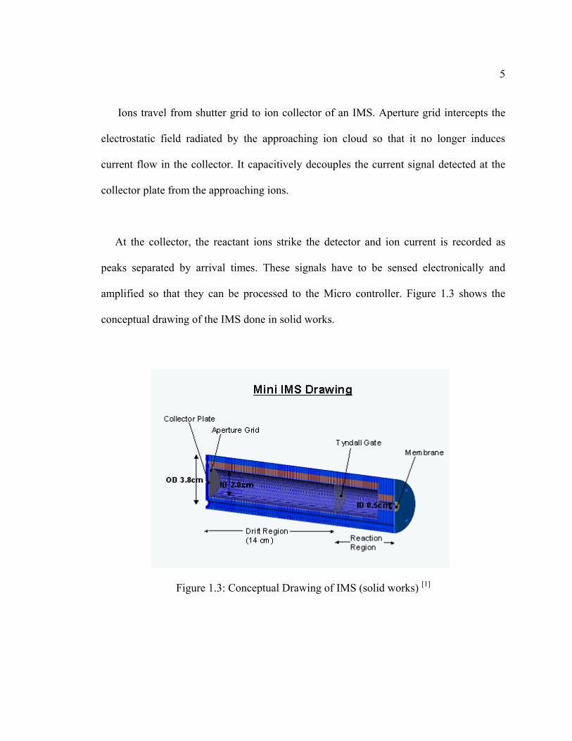
5
Ions travel from shutter grid to ion collector of an IMS. Aperture grid intercepts the
electrostatic field radiated by the approaching ion cloud so that it no longer induces
current flow in the collector. It capacitively decouples the current signal detected at the
collector plate from the approaching ions.
At the collector, the reactant ions strike the detector and ion current is recorded as
peaks separated by arrival times. These signals have to be sensed electronically and
amplified so that they can be processed to the Micro controller. Figure 1.3 shows the
conceptual drawing of the IMS done in solid works.
Figure 1.3: Conceptual Drawing of IMS (solid works) [1]

6
DESIGN REQUIREMENTS
High Voltage Power Supply The IMS requires a high voltage across the drift tube. We need to maintain a uniform
potential difference of about 500V/cm along the drift tube. The length of the drift tube is
4cm for the proposed design. So, for the miniature IMS we need a 2KV power supply.
The drift tube consists of resistors connecting stacks of conductor rings. The resistors
form a combined IMS load of 20 MΩ.
In addition to the signal preprocessing, the microprocessor uses digital channels to
control the timing of the high voltage pulse, the ion shutter, and system-level functions
such as gas turn-on and drift tube purge. A 0-5V pulse signal from the PIC is to be used
to control [turn on and off] the power supply.
The requirements can be listed as follows:
a) A precise 2KV power supply for a 20 MΩ load controlled with a 0-5V signal
from the PIC,
b) Use a nominal 1W power supply,
c) Cost should be a minimum [around $150-$200].
d) The PC board size should be 15cm x 3cm x 0.85cm.

7
Sensing Circuitry
The purpose of the sensing circuitry is to amplify, and digitize small output signals
from the IMS. The complete IMS signal occurs within a 20ms period. The peak spikes in
the IMS signal occur within a time period of 0.5-1 ms. The sampling rate would be 50us
so that we get 10-20 samples for every IMS spike and the peak of the spike is not missed.
So, the sensing circuit should provide the amplified value of the signal atleast for every
50us.
The microcontroller in the sensor scheme uses its own Vdd [5V] as a reference
voltage and does not support incoming signals higher than Vdd. So the sensing circuit
output should be limited to the maximum voltage input of the microcontroller, Vdd.

8
CHAPTER 2: DESIGN OF POWER SUPPLY Our main aim was to build a cheap, low power consuming voltage supply for the IMS.
There are power supplies available commercially that can supply high voltages, but size
is a big constraint. And power supplies with small size are very expensive. Voltage
converters can generate the desired voltage levels, and charge pumps are often the best
choice for applications requiring some combination of low power, simplicity, and low
cost. Charge pumps are easy to use and do not require expensive components.
The design consists of a high voltage charge pump and a level shifting control circuitry.
We selected a 1.25W, 200V [input 12V DC] power supply for this purpose. Figure 2.1
shows the block diagram of the scheme.
Figure 2.1: Block diagram of Power supply scheme

9
A brief description of the various components involved is given below
1) DC power supply: A dc power supply of 12V is used as the power source for the
level translator circuit.
2) DC-to-DC Converter: A dc power supply is used which generates 200V from a
12V input.
3) Protection Circuits: Protection circuits are used with both the dc power supplies to
protect them from negative voltages. One circuit is used to protect high voltage
transistors from breakdown.
4) Level Translator Circuits: Two level translator circuits are employed. One is used
to convert the 0-5V signal from the PIC to a 0-12V signal. The new signal is fed
to the second level translator circuit, which changes it to a 0-200V signal.
5) Charge Pump Circuit: This circuit pumps up the 200V voltage from the DC power
supply to 2KV. It consists of multiple stages pumped with two non-overlapping
oscillators [0-200V].

10
CHAPTER 3: DESIGN OF LEVEL TRANSLATOR CIRCUITS
LEVEL TRANSLATOR 1
The control signal from the PIC is a 0-5V pulse. It is level shifted to a 0-12V pulse
with a string of inverters. Figure 3.1 shows the schematic of the circuit.
Figure 3.1: Schematic of the level translator circuit
The 0-5V pulse from the PIC is level shifted to 0-12V using a string of inverters. Each
of the inverters labeled as U1, U2, ..U6 has an NMOS and PMOS. The schematic of each
of the inverters is shown in figure 3.2.
12 0
12 0 5
0
12 0
12 0

11
Figure 3.2: Schematic of the inverters [labeled as U]
The resistor R is used to reduce power consumption. It limits the current that can flow
to the circuit. When the input is at 5V, the PMOS should be OFF. In other words, the
Source to Gate voltage, Vsg of the PMOS should be less than the threshold voltage.
Some voltage is dropped across the resistor R1 and hence Vsg is reduced. Large resistor
for R1 would shut the PMOS off when input is 5V and reduce the power consumption,
but this will affect the output pulse [slow rise time].

12
SPICE SIMULATIONS Figure 3.3 shows the spice simulation of the level translator. Top trace is the 0-5V
input signal to the translator and the bottom trace is the 0-12V output of the level
translator at the output node of U1.
Figure 3.3: Simulation showing PIC signal [top] and the level translator’s output Ideally, either the NMOS or PMOS in the inverter is ON at any given time. But that is
not the case practically. During transition period [mid-way between low-to-high
transition] or for a particular range of voltages, there is always a period in which both the
NMOS and PMOS are ON. This creates a low resistance path from VDD to ground and
there is scope for large current to flow. This is called Contention current or Short Circuit
current. Figure 3.4 shows the spice simulation of the contention current seen in the first
inverter of the level translator.

13
Figure 3.4: Simulation showing the output transition and contention current [in red]
Efficiency of the level translator is reduced due to this contention current. As seen in
the below simulation, when the input pulse is at 3V, the NMOS is completely ON, but the
PMOS is not OFF yet. A resistor of 200ohms was used. The rise time will be greater than
the fall time. This can be seen in the simulations too and also in the measured results.
Figure 3.5 shows the rise time of the inverter and figure 3.6 shows the fall time of the
inverter. The rise time is around 80ns and the fall time is around 8ns.

14
Figure 3.5: Simulation showing the rise time of the inverter [80ns]
Figure 3.6: Simulation showing the fall time of the inverter [8ns]

15
MEASURED RESULTS
Figure 3.7 shows the measured results on the printed circuit board. The bottom trace
shows the 0-5V CLK input and the top trace is the 0-12V output generated.
Figure 3.7: Measured results on the PCB
Figure 3.8 shows the measured rise time of the inverter and figure 3.9 shows the
measured fall time of the inverter. The rise time was 90ns and the fall time was 20ns,
values close to the simulated values.

16
Figure 3.8: Rise time of the inverter measured on the PCB [90ns]
Figure 3.9: Fall time of the inverter measured on the PCB [20ns]
17
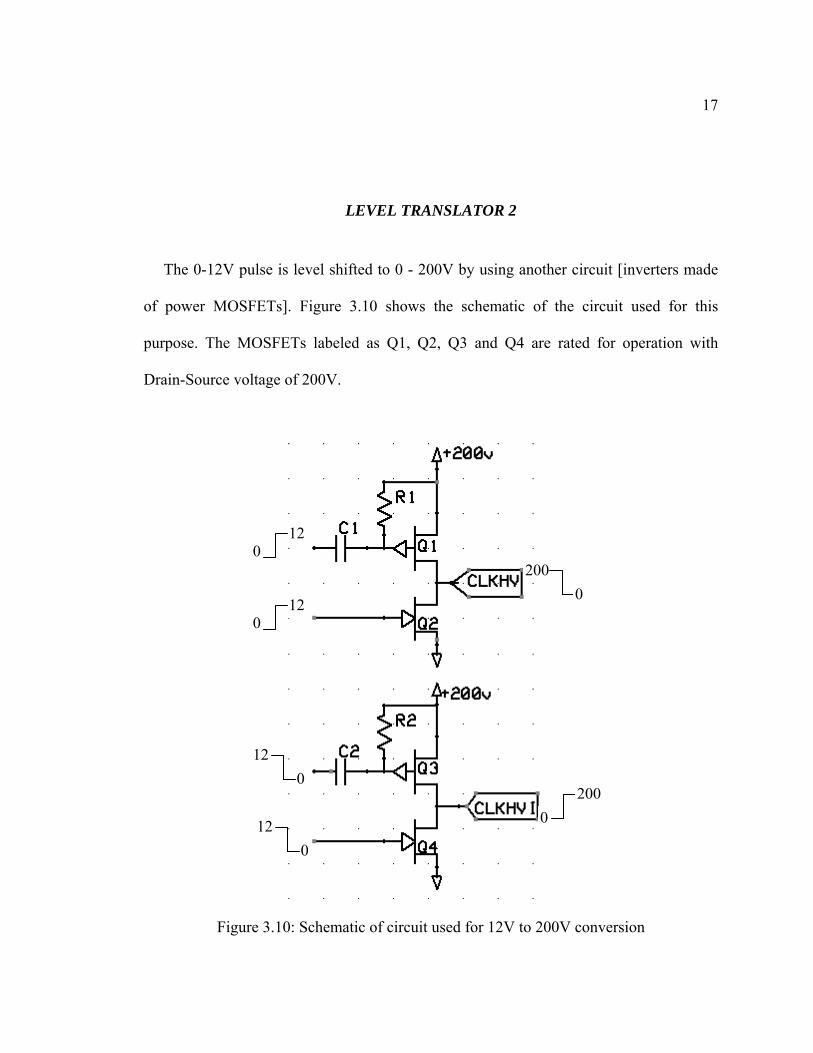
LEVEL TRANSLATOR 2
The 0-12V pulse is level shifted to 0 - 200V by using another circuit [inverters made
of power MOSFETs]. Figure 3.10 shows the schematic of the circuit used for this
purpose. The MOSFETs labeled as Q1, Q2, Q3 and Q4 are rated for operation with
Drain-Source voltage of 200V.
Figure 3.10: Schematic of circuit used for 12V to 200V conversion
200 0
12 0
12 0
12 0
12 0
200 0

18
When the input is at 0V, the source and gate of PMOS [Q1/Q3] are at 200V. Since
Vsg is 0V, they turn on and charge the output node to 200V. When the input swings to
12V, the Vgs of NMOS [Q2/Q4] is greater than the threshold voltage and so, they turn
ON. This pulls the output node to 0V.
With one plate of the capacitor [C1/C2] tied to 0-12V pulse, the gates of the PMOS
swing between 188V – 212V. The voltage on the gates will look as in figure 3.11
Figure 3.11: Voltage shifts on the gate of the MOSFETs Q1/Q3
We see an issue here. When the input is at 12V, the voltage on the gate is 212V. If the
clocking frequency is fast, the voltage on the gate may not discharge fully to 200V before
the next transition occurs. When the input changes from 12V to 0, the voltage on the gate
will not go all the way to 188V. It may stay at a higher voltage [more than the threshold
200 V
212 V
197 V
200 V
212 V
188 V
200 V
RC= 1us
Ideal Case
With fast clocking frequency

19
voltage of the PMOS] causing the PMOS to remain off when it should have been on.
To avoid this situation, diodes D1 and D2 are used to clamp the gates of the PMOS to
200V faster [way faster than the RC time constant]. The clamping mechanism of the
diode is very important to reduce the imperfections in the operation of the circuit when
the clock time period is less than the discharging time of the R-C network.
The total schematic of both the level translator circuits is shown in figure 3.12
Figure 3.12: Combined schematic of the level translators.

20
SPICE SIMULATIONS
Figure 3.13 shows the voltage on the gate of Q1 [pmosfet] in level translator 2. Top
view clearly shows the gate switching from 189V [ON] to 200V [off].
Figure 3.13: Voltage switching on the gate of the PMOSFET Q1

21
Figure 3.14 shows the high voltage clocks CLKHV and CLKHVI generated from
the level translator.
Figure 3.14: CLKHV and CLKHVI from simulations.

22
PROTECTION CIRCUITS
Consider the figure 3.15 showing an expanded schematic view of the translator
circuits which generate one phase of the clock.
Figure 3.15: Expanded schematic view of one phase of the clock
Initially the capacitor ‘C1’ is charged to 200V through the ‘R7’ resistor. A 1000pF
capacitor and a resistor of 1Meg were used. The clock pulse from the PIC should be
applied to the circuit only after the capacitor is given enough time to charge to 200V
[around 3RC=3.5ms]. This ensures that the PMOS devices used in the second level
translators do not breakdown.
200 0
5 0

23
If the R-C circuit was removed and the 12V clock signal was applied directly to the
PMOS transistor, then the Source to Gate Voltage VSG for the PMOS would be
VSG= 200-12 = 188V, if the input is high (12V)
VSG= 200 - 0 = 200V, if the input is low (0V)
But the maximum gate to source voltage is 20V. So, this can break the PMOS
transistor. The NMOS transistor (ZVNL120A) does not require such protection circuit
since the source is grounded and gate to source voltage is nominal.
The 12V power supply voltage is not ideal and may have small variations. So
decoupling capacitors are connected across the power supply terminals to smoothen out
the signal. This also reduces the ground bounce [2]. Ground bounce is the term used to
determine the increase in the potential of ideal ground potential due to the resistance of
the ground rail. When a current flows through the circuit, the resistance of the ground rail
tends to change the effective potential to a potential higher than zero volts. Placing a
capacitor pulls the node to zero. A diode is placed on the input and the output to cut off
the power supply if a negative voltage is applied. Figure 3.16 shows the power supply
protection circuit.
Figure 3.16: Power supply protection circuit.

24
A B C
CHAPTER 4: DESIGN OF CHARGE PUMP
Charge pumps are often the best choice for powering an application requiring a
combination of low power and low cost. A common problem in system engineering is
having a subsystem whose power requirements are not met by the main supply. Voltage
converters can generate the desired voltage levels, and charge pumps are often the best
choice for applications requiring some combination of low power, simplicity, and low
cost. Charge pumps are economical to use, because they require no expensive inductors.
The charge pump used was a high voltage Dickson’s charge pump [4]. This works on
alternately charging and discharging capacitors using two complementary clocks. The
clocks swing from 0 to 200V and are generated using the level shifting circuitry. Figure
4.1 shows the schematic of the charge pump used with 12 stages.
Figure 4.1: Schematic of the charge pump.

25
When CLKHV is low, node A is at (200- Vd), where Vd is the voltage drop across
the diode. When CLKHV goes high, the node A goes up to (2*200- Vd) . Node B is
charged to (400-2Vd). In the next cycle, when CLKHVI goes high, node B goes up to
(600-2 Vd). So node B swings from (400-2Vd) to (600-2 Vd). Node C swings from (600-2
Vd) to (800-2 Vd). In this way, the charge pump action proceeds through the circuit. So
the output of the charge pump swings from (n*200- n*Vd) down to [n*200- (n+1)*Vd].
The load capacitor is made larger than other capacitances to reduce this swing (ripple).
The diodes are selected such that their reverse breakdown voltage is greater than
200V. We selected the 1N4004 high voltage diode with a peak reverse voltage rating of
400v. For the 200V power supply we used 12AS200S, which is a 1.25W, 12V – 200V
power supply.
The number of stages required to generate 2kv from a 200V source can be estimated
as follows. The output of an N-stage charge pump swings from (N*200- N*Vd) down to
[N*200- (N+1)*Vd]. For simplicity, it is assumed that the forward voltage drop of the
diodes is negligible.
Output of charge pump = Vout = N*VDD ……………………. (4.1)
The load resistance at the output of the charge pump circuit discharges the last
capacitor when CLKHVI is low. So, the voltage drop due to this in one clock cycle can
be estimated as
26
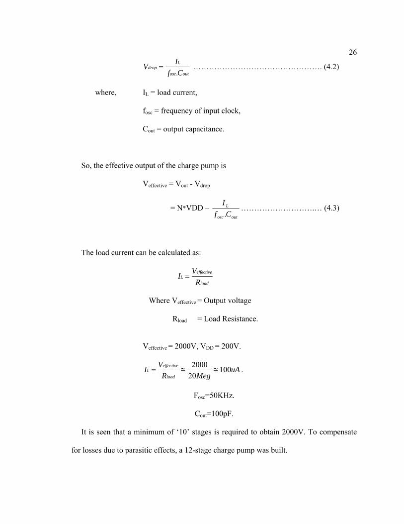
outosc
Ldrop
CfIV.
= …………………………………………. (4.2)
where, IL = load current,
fosc = frequency of input clock,
Cout = output capacitance.
So, the effective output of the charge pump is
Veffective = Vout - Vdrop
= N*VDD – outosc
L
CfI.
……………………….… (4.3)
The load current can be calculated as:
load
effectiveL
RVI =
Where Veffective = Output voltage Rload = Load Resistance. Veffective = 2000V, VDD = 200V.
uAMegR
VIload
effectiveL 100
202000
≅≅= .
Fosc=50KHz.
Cout=100pF.
It is seen that a minimum of ‘10’ stages is required to obtain 2000V. To compensate
for losses due to parasitic effects, a 12-stage charge pump was built.

27
From equation (4.3) we can observe that:
1) Charge pump output increases with an increase in the number of stages.
2) The output voltage increases with increase in frequency. But it will stay constant
after the frequency has reached a threshold value because the second term
becomes negligible for higher frequencies.
3) Output voltage also increases with a decrease in the output capacitance. However,
this increases the ripple on the output due to fast discharge time of the R-C
network on the output. Increasing the load resistance can reduce the ripple while
still using a lower output capacitance on the output compared to other capacitors.
4) Increasing the supply voltage VDD can also increase the output voltage but this in
turn reduces the power efficiency of the circuit.
The simplicity in equation 4.3 was achieved by neglecting the forward bias voltage
drop of the diode (around 1V) and also by neglecting the parasitic (stray) capacitances.
Due to parasitic capacitances, the charge sharing between the capacitors at the rising and
falling edges of the clocks is reduced and this degrades the performance of the circuit.
The voltage divider on the output of the charge pump is used to generate a feedback
signal to the PIC. This can be used to precisely control the output voltage at 2KV.

28
SIMULATION RESULTS:
Figure 4.2 shows the final simulation result of the power supply circuit. The control
signal from the PIC is delayed by 4ms, to allow for the gates of the high voltage PMOS
transistors to charge to 200V. Figure 4.3 shows the feedback signal across the 40K
resistor [2kv across 20Meg:40K resistive divider], which goes to the PIC.
Figure 4.2: Final simulated output of the power supply circuit [2kV]

29
Figure 4.3: Feed back signal from the power supply circuit to the PIC
30
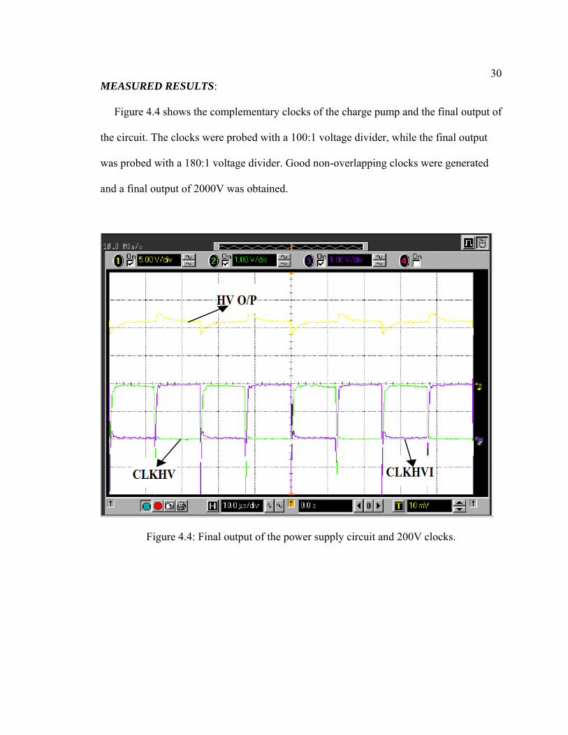
MEASURED RESULTS:
Figure 4.4 shows the complementary clocks of the charge pump and the final output of
the circuit. The clocks were probed with a 100:1 voltage divider, while the final output
was probed with a 180:1 voltage divider. Good non-overlapping clocks were generated
and a final output of 2000V was obtained.
Figure 4.4: Final output of the power supply circuit and 200V clocks.

31
CHAPTER 5: BUILDING PC BOARDS & TESTING CIRCUITS
The circuit was built on a Printed Circuit Board. The schematic and layout of the
whole circuit was drawn in Express PCB. Express PCB is a free CAD tool available at
www.expresspcb.com. The circuit boards were ordered using this service. The PCB
layout of the power supply is shown in figure 5.1. The red traces are laid on the front side
of the board and the green traces are laid on the back side of the board. The thick green
trace on the bottom is the ground rail. It is laid out very wide to decrease resistance and
eliminate ground bounce.
Figure 5.1: Printed Circuit Board Layout of the power supply circuit
Power Supply Trace
Ground TraceTransistors 12V-200V DC-DC Converter
Ceramic Capacitors

32
The prototype of the power supply board with all the components soldered is shown
in figure 5.2.
Figure 5.2: Final prototype of the power supply circuit
Testing the PC Boards
The testing is done in a systematic way.
1) First of all, the 5v to 12v level shifting circuitry is soldered and tested.
2) Then, the 200V power supply and the 12V to 200V level-shifting circuitry is
soldered.
Power Supply
Ceramic Capacitor
Transistors
Diode
Printed wires Resistors

33
3) The 12V DC supply is turned ON and then the control signal is turned ON. The
order is important because the gates of the PMOS should be charged to 200V
before the transistor switching action starts.
4) The 200V complementary clocks can be verified on the oscilloscope using a 100:
1 voltage divider. The oscilloscope inputs are rated for a maximum of 20V. So
care should be taken during testing, not to connect high voltage nodes directly to
the oscilloscope.
5) The charge pump circuit is then soldered. The pumped output of the circuit can be
measured with a high voltage probe in a multi-meter.
The figure 5.3 shows the equipment used to test the circuits on PC boards. The
equipment consists of an Oscilloscope, function generators, multi-meters and DC power
supplies.
Figure 5.3: Equipment used to test the PCB circuits
Oscilloscope
Multimeter
Function generator
DC power supply

34
The table below describes the apparatus used and their function.
Table 5.1 Apparatus used for testing
Apparatus Name Type Function
Multimeter HP 34401A Used to measure voltages,
currents and impedances
between nodes.
Function generator HP 33120A To generate a pulse waveform
(used as the control signal for
the circuit).
DC Power Supply HP E3631A To provide DC voltage.
Oscilloscope HP infinium Provides real time display of
waveforms.
Soldering Station AUTO-TEMP 379 Used to solder the components
onto the PCB.

35
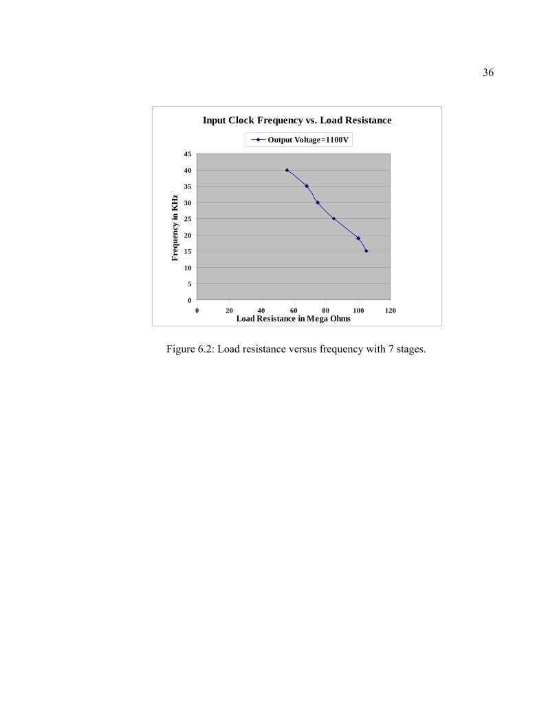
CHAPTER 6: PERFORMANCE AND RESULTS
Variation of load vs input clock frequency
The actual load of the power supply [the IMS] is subject to a 20MΩ + 30% variation
depending on how effectively the resistor material is printed on the LTCC conductors. As
the load resistance increases, the input clock frequency must be decreased to obtain the
same output voltage. Figure 6.1 shows a plot of load resistances and the input frequencies
to obtain an output voltage of 2000V. Figure 6.2 shows a plot of load resistances and the
input frequencies to obtain an output voltage of 1100V.
Input Clock Frequency vs. Load Resistance
0
10
20
30
40
50
60
0 50 100 150 200 250Load Resistance in Mega Ohms
Inpu
t Fre
quen
cy in
KH
z
Output Voltage=2000V
Figure 6.1: Load resistance versus frequency with 12 stages.
36
Input Clock Frequency vs. Load Resistance
0
5
10
15
20
25
30
35
40
45
0 20 40 60 80 100 120Load Resistance in Mega Ohms
Freq
uenc
y in
KH
z `
Output Voltage=1100V
Figure 6.2: Load resistance versus frequency with 7 stages.

37
Output Voltage Variation with Number of Stages The output voltage is primarily dependent on the number of stages used in the
multiplier circuit. As the number of stages increases, the output voltage also increases.
The voltage increase is basically due to increase of the charge being stored in each
capacitor from stage to stage. Figure 6.3 shows the output voltage variation with the
number of stages.
0
500
1000
1500
2000
2500
0 1 2 3 4 5 6 7 8 9 10 11 12 13 14Number of Capacitors / Stages
Out
put V
olta
ge (V
)
Rload=47Meg, Frequency=50KHz, Vdd=12V
Figure 6.3: Output Voltage vs. Number of Stages in Charge Pump

38
EFFICIENCY The power efficiency of the circuit can be defined as the ratio of the power delivered
to the load to the total power supplied by the source [5]. Mathematically,
)100.(..%
DDDD
loadload
IVIV
=η …………………………… (6.1)
where, η=power efficiency.
Vload = Output voltage at the load.
Iload = Current supplied to the load.
VDD = Supply Voltage.
IDD = Current supplied by VDD.
The efficiency of the charge pump is directly dependent on the 12V-200V DC-DC
converter. The charge pump is powered by an off-the-shelf 200 V power supply. The
power efficiency of the power supply is 78% at full-load [7].
The efficiency of the charge pump circuit developed in this project with 12 stages was
around 10% running at 50 KHz.

39
CONCLUSION A charge pump power supply circuit with a size of 1.2” x 6” was built and tested. A
level translator circuit is used to convert the 0-5V control input to a 0-200V clock pulse.
The voltage multiplier is based on a simple Dickson charge pump principle.
The output voltage was linearly increasing with increase in number of stages (diode-
capacitor pairs) as seen in figure 6.3. Power consumed by the circuit is 1.25W and the
output voltage generated with the prototype is 2000V. Typical clock frequencies vary
between 10-100KHz depending upon the load resistance. Power efficiency of the charge
pump circuit is around 9%. The circuit exhibits good tolerance to supply voltages and
load resistances.
Future Work Low power efficiency of the circuit can be attributed to the power loss in the level
translator circuit. Further modifications to the level translator circuit should be made to
increase the overall power efficiency. Contention current should be reduced in the 5V to
12V level translator.
Higher clock frequencies can be applied by decreasing the series resistance in the
inverter block, but this will increase the power consumption of the circuit. The feedback
circuit for the charge pump controlling the frequency of the input clock signal should be
integrated with the PIC.

40
CHAPTER 7: SENSING CIRCUIT
At the end of the Ion Mobility Spectrometer is a collector plate, which collects ions
and delivers a time dependent signal corresponding to the mobility of the arriving ions.
The resulting output signal comprises of peaks corresponding to the various compounds
in the mixture. Such an ion mobility spectrum consists of information about different
trace compounds present in the sampled gas.
The complete IMS signal occurs within a 20ms period. The peak spikes in the IMS
signal occur within a time period of 0.5-1 ms. The series of peaks have to be amplified
and digitized such that they can be fed into the micro controller. An ADC architecture is
needed for this purpose.
Figure 7.1: Typical output signals from the IMS [16]

41
Traditional ADC architectures like successive approximation converters and dual-
slope converters provide high resolution, but trimming is needed for accuracy. They
provide high resolution at the expense of using high-speed and high accuracy integrators
and high-precision sample and hold circuits. Over sampling ADCs are preferred over
these because, they achieve high resolution with digital signal processing techniques used
in place of precise and complex analog components [3].
The signal is sampled at a rate much higher than the signal bandwidth, so aliasing is
not a major factor. If we consider the frequency domain representation of an
oversampling converter, the frequency spectra are widely spaced. So, there is no problem
of frequency spectra overlap and aliasing. So compared to Nyquist rate converters,
oversampling ADCs achieve higher resolution, need simple anti-aliasing circuitry and
less analog circuitry, have accuracy independent of component matching. The only
disadvantage compared to Nyquist rate converters is that they take more time to sample
the input resulting in less throughput. So, oversampling ADCs tradeoff time resolution
for amplitude resolution [6].
Figure 7.2: Frequency domain for an oversampling converter.
0 -fs fs f

42
Figure 7.3 shows the block diagram of an oversampling ADC. The input signal is
sampled, quantized and digitized. The modulator outputs a pulse-density modulated
signal, which represents the average of the input signal. This type of modulation is
referred to as sigma-delta or delta-sigma modulation. The oversampling converter can
take hundreds of samples over a period of time to output a pulse density signal. Digital
filters are used to filter the quantization noise and attenuate spurious signals.
Analog input Digital Output
Figure 7.3: Block diagram of an oversampling ADC
ΔΕ Modulator
Digital Filter

43
First Order ΔΕ Modulator
A first order ΔΕ modulator can be conceived with an integrator, a 1-bit ADC and a 1-
bit DAC in the feedback path. Figure 7.4 shows a basic first order ΕΔ modulator.
Figure 7.4: Basic first order delta sigma modulator
The output of the integrator can be written as
u(nT) = integrator’s previous input + integrator’s previous output
= [x(nT-T) – q(nT-T)] + u(nT-T) ……………………….……….. (7.1)
where T = 1/fs = 1/sampling frequency,
n is an integer value.
The 1-bit ADC can be realized with a simple comparator, which converts an analog
signal into either a high or a low. The 1-bit DAC sums +VREF to the input if the
comparator output is low and –VREF if the comparator output is high.
Integrator
y(nT) u(nT)
q(nT)
x(nT) Delay 1-bit ADC
1-bit DAC

44
The quantization error associated with the 1-bit ADC can be written as
Qe(nT) = y(nT) – u(nT) ………………………………………. (7.2)
Plugging equation 7.2 in equation 7.1, the output of the modulator is
y(nT) = Qe(nT) + x(nT-T) – [q(nT-T) – u(nT-T)] …………………………. (7.3)
Assuming the 1-bit DAC to be ideal, we can write
y(nT) = q(nT) …………………………………………… (7.4)
Using equations 7.4 and 7.2 in equation 7.3, we get
y(nT) = Qe(nT) + x(nT-T) – [y(nT-T) – u(nT-T)]
y(nT) = x(nT-T) + Qe(nT) - Qe(nT-T) ………………………………… (7.5)
From equation 7.5, we can observe that, the output of the sigma delta modulator
consists of a quantized value of the input signal delayed by one sample period and a
difference of quantization error between present and preceding values. So, to a first order,
quantization noise cancels itself.
Frequency Domain Analysis
Figure 7.5 shows a model of first order modulator in the s domain. The integrator is
represented with its ideal transfer function of 1/s. The 1-bit ADC can be represented with
a simple error source, Qe(s). The 1-bit DAC is assumed to be ideal.

45
Figure 7.5: Frequency domain model of a first-order delta-sigma modulator
The output of the modulator can be written as
vout(s) = Qe(s) + s1 .[vin(s) – vout(s)]
vout(s) = Qe(s) 1+s
s + vin(s) 1
1+s
The modulator behaves as a low-pass filter on the input signal and as a high-pass filter
on the quantization noise. If we observe the frequency response of the modulator (shown
in Figure 7.6), we see that in the region of input signal, the signal has high gain while the
noise has a small value. At higher frequencies beyond the bandwidth of the input signal,
quantization noise increases. This high-pass characteristic of pushing the noise out of the
bandwidth of the input signal is called Noise Shaping [3].
q(s)
vin(s) vout(s)
Qe(s)
s1

46
Figure 7.6: Frequency response of the first-order delta sigma modulator.
By oversampling, the noise bandwidth is distributed over a wider bandwidth as shown
in figure 7.7. If a digital low pass filter is applied to the modulator output, much of the
quantization noise is removed without affecting the wanted signal. Sigma-delta
modulator shapes the quantization noise so that most of it lies above the pass band of the
digital output filter. So, a high resolution A/D conversion can be obtained with a low
resolution ADC.
ω
Bandwidth of the modulator
Signal bandwidth
vout
|Qe . 1+s
s |
|vin . 1
1+s
|

47
Figure 7.7: RMS quantization noise in a typical ADC with sampling frequency fs
Figure 7.8: RMS quantization noise in an over sampled ADC (sampling frequency Kfs)
SIGNAL OUTPUT
fs/2 fs
fs
ADC
RMS Quantization noise
Kfs/2fs
SIGNAL OUTPUT
fs/2
Kfs
ADC LPF
RMS Quantization noise removed by filtering
Filter Passband

48
Since the digital output filter reduces the bandwidth, the output data rate may be
lower than the original sampling rate and still satisfy the Nyquist criterion. This can be
achieved by passing every Mth result to the output and discarding the rest. This process is
known as ‘Decimation by a factor of M’. M can be any integer value, provided that the
output data rate is more than twice the signal bandwidth. Decimation does not cause any
loss of information.

49
CHAPTER 8: SIMPLE NOISE-SHAPING MODULATOR
Figure 8.1 shows a continuous time implementation of a first order noise-shaping
modulator. This is simple to implement and easy to test on the bench. It consists of an op-
amp, a comparator, capacitors and resistors.
Figure 8.1: Analog implementation of a first order Noise shaping modulator
Spice simulations are used to demonstrate the operation of this modulator. The
sampling frequency is assumed to be 32MHz and the input signal used is a 100KHz
sinusoidal wave with peak amplitude of 2.0V and centered around VCM. VDD=5V and
VCM = 2.5V. Ideal spice models were used for the opamp and comparator in the
simulations.
CLK, clocked at fs
VCM
R
C
R VCM
VOut

50
Figure 8.2 shows the spice simulation result with the input and output signals of the
modulator. We can clearly see that the average of the output of modulator tracks the
input. When the input is at its maximum amplitude, the output of the modulator stays
high [logic one] for the most part. If the input is at its minimum amplitude, the output of
the modulator stays low [logic zero] for the most part. When the input signal level is
moving through the common mode voltage, the modulator output bounces between VDD
and ground, so that the average value matches the input value.
Figure 8.2: Spice simulation of a first order NS modulator in figure 8.1
This 1-bit output of the modulator can be connected to a digital averaging filter to get
a higher resolution output. The output of the filter would be a digital word representing
the analog input voltage.

51
Modulation Noise In a First Order NS Modulator
From equation 7.5, the output of the NS modulator in the time domain is
y(nT) = x(nT-T) + Qe(nT) - Qe(nT-T)
Modulation noise is the differentiated quantization noise. In the z-domain, the block
diagram of the NS modulator can be represented as shown in Figure 8.3
Figure 8.3: z-domain representation of the NS modulator
So, the output of the modulator is related to the input as shown in
Y(z) = )()(1
)( zXzA
zA⋅
++ )(
)(11 zQ
zA⋅
+
Assuming A(z) = z-1, this can be re-written as
Y(z) = z-1 X(z) + (1-z-1) E(z) …………………………………. (8.1)
The product of the noise transfer function and modulation noise can be written as
NTF(z).E(z) = (1-z-1) E(z) ………………………………….. (8.2)
ADC
Sigma Delta
X(z) Y(z)
Q(z)
A(z)
1-bit DAC

52
The noise voltage spectral density is given by
VQe(f) = s
LSB
fV12
So, in the frequency domain, equation 8.2 can be written as
NTF(f). VQe(f) = (1- sffj
eΠ− 2
). s
LSB
fV12
The power spectral density, PSD of the modulator’s Modulation Noise can be written
as[3]
|NTF(f)|2 . | VQe(f)|2 = s
LSB
fV12
2
. 2 (1- cos2sf
fΠ ) ,V2/Hz ………………(8.3)
Figure 8.4 shows the theoretical PSD from the above equation with
VLSB = 5V [1-bit ADC/DAC in the modulator]
fs = 32MHz,
fn = fs/2 = 16MHz.

53
Figure 8.4: Theoretical Modulation noise for a first order NS modulator
From figure 8.4, we can see that the modulation noise is significant. But by restricting
the bandwidth of the modulation noise, we can considerably reduce the RMS
quantization noise.
The modulation noise spectrum of the first order NS modulator in figure 8.1 can be
viewed in SPICE. A slow moving voltage ramp is given as the input to the modulator.
The difference between the input and output of the modulator is the modulation noise.
Frequency Mhz
V2/Hz x 10-9

54
Figure 8.5 shows the input and output of the modulator. Figure 8.6 shows the
modulation noise of the NS modulator in figure 8.1.
Figure 8.5: Slow ramp input to the modulator and its corresponding output

55
Figure 8.6: Modulation noise for a slow ramp input to the modulator
The PSD of the modulation noise can be obtained by squaring the magnitude of
modulation noise and dividing the result with the resolution of the Fourier transform
used. Figure 8.7 shows the PSD of the modulation noise. The shape of the modulation
noise spectrum is comparable to the theoretical noise spectrum in figure 8.4

56
Figure 8.7: PSD of the modulation noise for a slow ramp input to the modulator.
Ideal SNR of a First Order NS Modulator
The RMS quantization noise can be reduced by using simple averaging of ADCs
outputs. If K samples are averaged, the sampling frequency is effectively increased by K
times. The RMS quantization can be written as [3]
VQe,RMS = 12
.1 LSBVK
The ideal Signal to Noise Ratio in this case is

57
SNRideal = 20. RMSQe
p
VV
,
2log
SNRideal = 6.02N + 1.76 + 10logK ……………………………… (8.4)
So, every doubling in the oversampling ratio results in a 0.5 bit increase in resolution.
Consider now the case of a first-order NS modulator with K of its output samples
averaged. Assuming f ≤ fn and the output of the modulator is passed through a perfect
low pass filter, equation 8.3 can be rewritten as
|NTF(f)| . | VQe(f)| = s
LSB
fV12
. 2sinsff
Π V/√Hz
The RMS quantization noise introduced in a bandwidth B can be calculated as
V2Qe,RMS = 2 ∫
BQe dffV
0
2 ).(
V2Qe,RMS = 2 ∫
B
0|NTF(f)|2 . | VQe(f)|2 . df
V2Qe,RMS = 2 .
s
LSB
fV12
2. ∫
B
04 sin2
sff
Π . df ……………………. (8.5)
The maximum bandwidth of the input signal can be written as
B = Kf s
2

58
where K= oversampling ratio, which is the number of output samples averaged.
Using this in equation 8.5 , we can write
VQe,RMS = 2/3
1312 K
VLSB ⋅Π
⋅
So, ideal data converter SNR using the first-order NS modulator can be written as [3]
SNRideal = 6.02N + 1.76 - 5.17 + 30logK …………………….. (8.6)
From this equation, we can see that every doubling in oversampling ratio results in
1.5bits increase in the resolution which corresponds to a 9dB increase in SNRideal. So for
this NS modulator with a 1-bit ADC, the final resolution [after digital filter] of the
resulting data converter is Ninc+1 bits, where Ninc is given as
Ninc = 6.02
5.17-30logK
Digital Filtering
The current peaks from the collector plate of the IMS occur in a time period of 0.5ms
to 1ms. The worst-case minimum time period is supposed to be 0.2ms. So, we have a low
frequency input signal to the modulator. The modulator’s resolution is greatly dependent
on the number of samples taken in a given time, KTs. Digital filtering can be done by

59
passing the output of the modulator to a single accumulate and dump circuit or a
counter. The output of the modulator can be band limited to fs/K

60
CHAPTER 9: IMPLEMENTATION OF THE SENSING CIRCUIT
The figure 9.1 shows schematic of the first order Delta Sigma modulator implemented
in this project work. When compared to figure 8.1 we can see that the clocked
comparator is implemented using a D flip-flop. By using discrete components to build the
modulator, we can precisely set the values of the resistors and capacitors.
Figure 9.1: Schematic of the first order Delta Sigma modulator implemented
The TLC2201 is a precision, low-noise opamp. It is used as an integrator with the non-
inverting input tied to a reference voltage [2.5V here]. The integrator accumulates the
difference between the input signal and fed back signal. This is compared with the
reference voltage using the LM339 comparator. The D flip-flop is used to clock the
comparator output. So, the LM339 comparator combined with the D flip-flop forms a

61
clocked comparator. The output of the modulator tracks the average of the input. The
average fed back signal would also ideally be the same as the input signal.
The figure 9.2 shows the printed circuit board layout of the modulator shown in figure
9.1. The component packaging style is chosen as DIP for ease of soldering to the PCB.
Decoupling capacitors are used on the power supply routing to smoothen out the signal.
Figure 9.2: PCB layout of the Delta Sigma modulator
Power Supply Trace
Ground Trace D flip-flopOpamp (TLC220x)
Comparator (LM339)

62
Figure 9.3 shows the response of the NS modulator for a sinusoidal input waveform
centered around VCM = 2.5V. The peak-to-peak amplitude of the input is 5V and running
at 10KHz. The output of the comparator is clocked at 10Mhz.
Figure 9.3: Measured response of the delta sigma modulator
DC Analysis:
A DC input signal to the modulator and varying the amplitude of the signal, the output
of the modulator was measured. Since the modulation noise is zero at DC, we can
measure the exact value of the input at the output. 10Mohm resistors were used for the
input and feedback resistors. The input was varied in steps of 10mV and the output

63
measured. The minimum resolution of input current was 1nA [10mV/10Meg]. Figure
9.4 shows the plot showing the modulator output voltage vs the input current.
DC Analysis
0.000
1.000
2.000
3.000
4.000
5.000
-2.5E-7 -2.0E-7 -1.5E-7 -1.0E-7 -5.0E-8 0.0E+0 5.0E-8 1.0E-7 1.5E-7 2.0E-7 2.5E-7
I/P current
O/P
vol
tage
Figure 9.4: DC analysis of the delta sigma modulator

64
CONCLUSION
A basic first order delta sigma modulator was built and tested on a Printed Circuit
Board. The size of the PCB built was 1.7”x4”. The first order ΔΕ modulator was
conceived with an integrator, a 1-bit ADC (comparator) and a 1-bit DAC in the feedback
path. The modulator outputs a pulse-density modulated signal, which represents the
average of the input signal.
The output of the sigma delta modulator consists of a quantized value of the input
signal delayed by one sample period and a difference of quantization error between
present and preceding values. To a first order, quantization noise gets cancelled. This is
achieved by pushing the noise out of the bandwidth of the input signal [Noise Shaping].
A high resolution ADC can be obtained with a 1-bit resolution ADC.

65
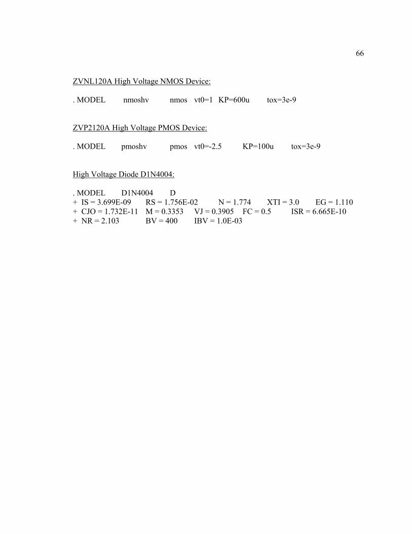
APPENDIX: SPICE MODELS AND NETLIST
SPICE MODELS
ZVN3306A NMOS DEVICE:
. SUBCKT ZVN3306A 3 4 5 * D G S M1 3 2 5 5 N3306M RG 4 2 270 RL 3 5 1.2E8 C1 2 5 28E-12 C2 3 2 3E-12 D1 5 3 N3306D * . MODEL N3306M NMOS VTO=1.824 RS=1.572 RD=1.436 IS=1E-15 KP=.1233 +CBD=35E-12 PB=1 . MODEL N3306D D IS=5E-12 RS= 0.768 . ends ZVP2106A PMOS DEVICE: . SUBCKT ZVP2106A 3 4 5 * D G S M1 3 2 5 5 MP2106 RG 4 2 160 RL 3 5 1.2E8 C1 2 5 47E-12 C2 3 2 10E-12 D1 3 5 DP2106 * . MODEL MP2106 PMOS VTO=-3.193 RS=2.041 RD=0.697 IS=1E-15 KP=0.277 +CBD=105E-12 PB=1 LAMBDA=1.2E-2 . MODEL DP2106 D IS=2E-13 RS=0.309 . ends
66
ZVNL120A High Voltage NMOS Device: . MODEL nmoshv nmos vt0=1 KP=600u tox=3e-9 ZVP2120A High Voltage PMOS Device: . MODEL pmoshv pmos vt0=-2.5 KP=100u tox=3e-9 High Voltage Diode D1N4004: . MODEL D1N4004 D + IS = 3.699E-09 RS = 1.756E-02 N = 1.774 XTI = 3.0 EG = 1.110 + CJO = 1.732E-11 M = 0.3353 VJ = 0.3905 FC = 0.5 ISR = 6.665E-10 + NR = 2.103 BV = 400 IBV = 1.0E-03

67
H-SPICE NETLIST [POWER SUPPLY] *Netlist . SUBCKT INVERTER VIN VOUT VDD X1 vout vin vdd1 ZVP2106A X2 vout vin 0 ZVN3306A R1 vdd vdd1 200 . SUBCKT ZVN3306A 3 4 5 * D G S M1 3 2 5 5 N3306M RG 4 2 270 RL 3 5 1.2E8 C1 2 5 28E-12 C2 3 2 3E-12 D1 5 3 N3306D . MODEL N3306M NMOS VTO=1.824 RS=1.572 RD=1.436 IS=1E-15 KP=.1233 +CBD=35E-12 PB=1 .MODEL N3306D D IS=5E-12 RS=.768 .ENDS . SUBCKT ZVP2106A 3 4 5 * D G S M1 3 2 5 5 MP2106 RG 4 2 160 RL 3 5 1.2E8 C1 2 5 47E-12 C2 3 2 10E-12 D1 3 5 DP2106 * . MODEL MP2106 PMOS VTO=-3.193 RS=2.041 RD=0.697 IS=1E-15 KP=0.277 CBD=105E-12 PB=1 LAMBDA=1.2E-2 . MODEL DP2106 D IS=2E-13 RS=0.309 . ENDS . ENDS

68
Vlow low 0 dc 12 Dlow LOW VDD D1N4004 CLOW VDD 0 1UF VCLOCK CLOCK 0 DC 0 AC 0 0 PULSE (0 5 4m 1N 1N 5U 10U) X1 CLOCK OUTPUT vdd0 INVERTER Xb1 OUTPUT clk vdd1 INVERTER Xb2 clk clki vdd2 INVERTER Xb3 clk ng vdd3 INVERTER Xb4 OUTPUT ngp vdd4 INVERTER Xb5 OUTPUT ngn vdd5 INVERTER VB0 VDD VDD0 0 VB1 VDD VDD1 0 VB2 VDD VDD2 0 VB3 VDD VDD3 0 VB4 VDD VDD4 0 VB5 VDD VDD5 0 M1 clkhv n3 hv0 hv pmoshv L=1u W=1000u M2 clkhv ng 0 0 nmoshv L=1u W=1000u R2 hv n3 1MEG Vd6 hv hv1 0v r11 HV1 HV0 200 D100 n3 hv D1N4004 C2 n3 clki 1000P R3 hv clkhv 500k M3 clkhvi n4 hv3 hv pmoshv L=1u W=1000u M4 clkhvi ngn 0 0 nmoshv L=1u W=1000u R4 hv n4 1MEG Vd7 hv hv4 0v R12 HV4 HV3 200 D101 n4 hv D1N4004 C3 n4 ngp 1000p R5 hv clkhvi 500k Vhv High 0 DC 200 DHIGH high HV D1N4004 Cmain hv 0 10u

69
*VOLTAGE MULTIPLIER Vd5 HV HV5 0v D1 HV5 A D1N4004 D2 A B D1N4004 D3 B C D1N4004 D4 C D D1N4004 D5 D E D1N4004 D6 E F D1N4004 D7 F G D1N4004 D8 G H D1N4004 D9 H I D1N4004 D10 I J D1N4004 D11 J K D1N4004 D12 K L D1N4004 C4 A CLKHV 100PF IC=0 C5 B CLKHVI 100PF IC=0 C6 C CLKHV 100PF IC=0 C7 D CLKHVI 100PF IC=0 C8 E CLKHV 100PF IC=0 C9 F CLKHVI 100PF IC=0 C10 G CLKHV 100PF IC=0 C11 H CLKHVI 100PF IC=0 C12 I CLKHV 100PF IC=0 C13 J CLKHVI 100PF IC=0 C14 K CLKHV 100PF IC=0 C15 L 0 100PF IC=0 R6 L M 20MEG R7 M 0 50K *. IC V (n3)=200 *. IC V (n4)=200 . Tran 1000n 8M UIC . MODEL D1N4004 D + IS = 3.699E-09 RS = 1.756E-02 N = 1.774 XTI = 3.0 EG = 1.110 + CJO = 1.732E-11 M = 0.3353 VJ = 0.3905 FC = 0.5 ISR = 6.665E-10 + NR = 2.103 BV = 400 IBV = 1.0E-03

70
. Model nmoshv nmos vt0=1 KP=600u tox=3e-9
. Model pmoshv pmos vt0=-2.5 KP=100u tox=3e-9
. Model nmoslv nmos vt0=1 KP=60u tox=30e-9
. Model pmoslv pmos vt0=-2.5 KP=10u tox=30e-9 . End

71
SPICE NETLIST [ 1st Order DSM]
* Netlist* .tran 20n 10u 0 20n uic * SPICE command scripts .control destroy all run plot Vout Vin ylimit 0 6 plot voutop .endc *Input power and references VDD VDD 0 DC 5 Vtrip Vtrip 0 DC 2.5 VCM VCM 0 DC 2.5 *Input Signal Vin Vin 0 DC 0 Sin 2.5 2.0 100k *Clock Signals Vphi1 phi1 0 DC 0 Pulse 0 5 0 200p 200p 15n 31.25n R1 vinm vin 10MEG R2 vinm vout1 10meg R3 phi2 0 1MEG *Use a VCVS for the op-amp Eopamp Voutop 0 VCM Vinm 100MEG *Setup switched capacitors and load CF Voutop Vinm 100p *clocked comparator implementation XSH VDD Vtrip Voutop Outsh phi1 SAMPHOLD S6 VDD Vout Vcm Outsh switmod S7 Vout 0 Outsh Vcm switmod

72
.model switmod SW RON=0.1 * Ideal Sample and Hold subcircuit .SUBCKT SAMPHOLD VDD Vtrip Vin Vout CLOCK Ein Vinbuf 0 Vin Vinbuf 100MEG S1 Vinbuf VinS VTRIP CLOCK switmod Cs1 VinS 0 1e-10 S2 VinS Vout1 CLOCK VTRIP switmod Cout1 Vout1 0 1e-16 Eout Vout 0 Vout1 0 1 .model switmod SW .ends Mn vout1 vout 0 0 cmosn L=2u W=3u Mp vout1 vout vdd vdd cmosp L=2u W=9u * Level 2 model nchan model for CN20 .MODEL CMOSN NMOS LEVEL=2 PHI=0.600000 TOX=4.3500E-08 XJ=0.200000U TPG=1 + VTO=0.8756 DELTA=8.5650E+00 LD=2.3950E-07 KP=4.5494E-05 + UO=573.1 UEXP=1.5920E-01 UCRIT=5.9160E+04 RSH=1.0310E+01 + GAMMA=0.4179 NSUB=3.3160E+15 NFS=8.1800E+12 VMAX=6.0280E+04 + LAMBDA=2.9330E-02 CGDO=2.8518E-10 CGSO=2.8518E-10 + CGBO=4.0921E-10 CJ=1.0375E-04 MJ=0.6604 CJSW=2.1694E-10 + MJSW=0.178543 PB=0.800000 * Weff = Wdrawn - Delta_W * The suggested Delta_W is -4.0460E-07 * Level 2 model pchan model for CN20 .MODEL CMOSP PMOS LEVEL=2 PHI=0.600000 TOX=4.3500E-08 XJ=0.200000U TPG=-1 + VTO=-0.8889 DELTA=4.8720E+00 LD=2.9230E-07 KP=1.5035E-05 + UO=189.4 UEXP=2.7910E-01 UCRIT=9.5670E+04 RSH=1.8180E+01 + GAMMA=0.7327 NSUB=1.0190E+16 NFS=6.1500E+12 VMAX=9.9990E+05 + LAMBDA=4.2290E-02 CGDO=3.4805E-10 CGSO=3.4805E-10 + CGBO=4.0305E-10 CJ=3.2456E-04 MJ=0.6044 CJSW=2.5430E-10 + MJSW=0.244194 PB=0.800000 * Weff = Wdrawn - Delta_W * The suggested Delta_W is -3.6560E-07

73
REFERENCES
[1] Donald G. Plumlee, Ion Mobility Spectrometer (IMS) Fabricated in Low
Temperature Co fire Ceramic (LTCC), IMPAS CII, April 9 2003,
http://coen.boisestate.edu/sensor/CMEMS/Presentations.htm
[2] R. Jacob Baker, Harry W. Li and David E. Boyce, CMOS Circuit Design, Layout
and Simulation, John Wiley and Sons publishers, ISBN-81-203-1682-7.
[3] R. Jacob Baker, CMOS MIXED-SIGNAL CIRCUIT DESIGN, John Wiley and
Sons Publishers, ISBN-0-471-27256-6.
[4] JOHN F. DICKSON, On-Chip High-Voltage Generation in MNOS Integrated
Circuits Using an Improved Voltage Multiplier Technique, IEEE Journal of Solid-
State Circuits, Vol. SC-11, No.3, June 1976.
[5] Janusz A. Starzyk, Ying-Wei Jan, and Fengjing Qiu, A DC–DC Charge Pump
Design Based on Voltage Doublers, IEEE Transactions on Circuits and Systems —
I: Fundamental theory and Applications, Vol.48, No.3, March 2001,pp. 350-359
[6] J. C. Candy and G. C. Temes (eds.), Oversampling Delta-Sigma Data Converters,
IEEE Press, 1992. ISBN 0-87942-285-8.
[7] Specification of the 12A200S DC-DC converter is available at
http://www.picoelectronics.com/dcdclow/pe62_63.htm
[8] Specifications of the ZVP2106A transistor:
http://www.zetex.com/3.0/pdf/ZVP2106A.pdf

74
[9] Specifications of the ZVN3306A transistor:
http://www.zetex.com/3.0/pdf/ZVN3306A.pdf.
[10] Specifications of the ZVP2120A transistor:
http://www.zetex.com/3.0/pdf/ZVP2120A.pdf
[11] Specifications of the ZVNL120A transistor:
http://www.zetex.com/3.0/pdf/zvnl120.pdf
[12] Specifications of the 1N4004 Diode:
http://www.fairchildsemi.com/ds/1N/1N4004.pdf.
[13] Specifications of the LM339 available at:
http://www.national.com/search/search.cgi/main?keywords=lm339
[14] Specifications of the 74HC74 available at:
http://www.standardproducts.philips.com/products/flipflops/74
[15] Specifications of the TLC220x opamp available at:
http://focus.ti.com/docs/prod/folders/print/tlc220x.html
[16] http://coen.boisestate.edu/sensor/WordFiles/ProgressReport12_23_02.htm