Embed Size (px)
Citation preview

Circuit Retiming with Interconnect Delay
CUHK CSE CAD Group Meeting OneEvangeline Young
Aug 19, 2003

Circuit Retiming
Given a circuit, we want to relocate the registers to achieve a better clock period.
Registers
Retiming
Clock period= 3 units
Clock period= 2 units

Circuit Retiming
In order to maintain the functionality of the circuit, registers can only be moved in certain ways:
Retiming

Circuit Retiming
Given a circuit, how should we place the registers to minimize the clock period?

Traditional Approach
This retiming problem is firstly introduced in the following classical paper: “Retiming Synchronous Circuitry”, Charles
E. Leiserson and James B. Saxe, Algorithmica, 6:5-35, 1991
Only gate delay was considered. Three methods are proposed. One of them so
lves the problem by mixed integer linear programming (MILP).

Traditional Approach
Notations: d(v) is the delay of node v. w(e) is the original no. of registers on edge e. c is the clock period that we want to check if it
is feasible. r(v) is the retiming value of node v, i.e., the no.
of registers moved from the output to the input of node v. (r(v) is what we want to find.)
s(v) is the longest delay from a register connected directly to node v to the output of v.

Traditional Approach
More about s(v)…
v
s(v) is the delay from point A to B,including the delay of v.
A
B

Traditional Approach
Integer Linear Program:
d(v) s(v) for all node v (1) s(v) c for all node v (2) r(u) r(v) w(e) for all edge e(u,v) (3) s(u) – s(v) -d(v) wherever e(u,v) s.t.
r(u) - r(v) = w(e)(4)

Traditional Approach
Write R(v) as r(v) + s(v)/c The ILP can be written as an MILP:
r(v) – R(v) -d(v)/c for all node v (1)
R(v) – r(v) 1 for all node v (2) r(u) r(v) w(e) for all edge e(u,v) (3) R(u) – R(v) w(e)-d(v)/c for all edge e(u,v)
(4)
The above set of difference constraints can be solved in polynomial time, though it consists of both integer and real variables.

Traditional Approach
Use binary search to find the optimal clock: T0 = 0
T1 = e10 // a large no. Repeat
c = (T0 + T1)/2 Check if c is a feasible clock period by solving the
MILP. If success, T1 = c; otherwise, T0 = c.
Until success and (T1 - T0)/T1 < ε

Retiming with Interconnect Delay
We consider clock period minimization. Retiming has been studied and applied
extensively at logic synthesis. However, most previous retiming algorithms
ignore interconnect delay. Interconnect delay should be considered for
high performance circuits in DSM design.
This solution is going to be presented in the upcoming ICCAD 2003.
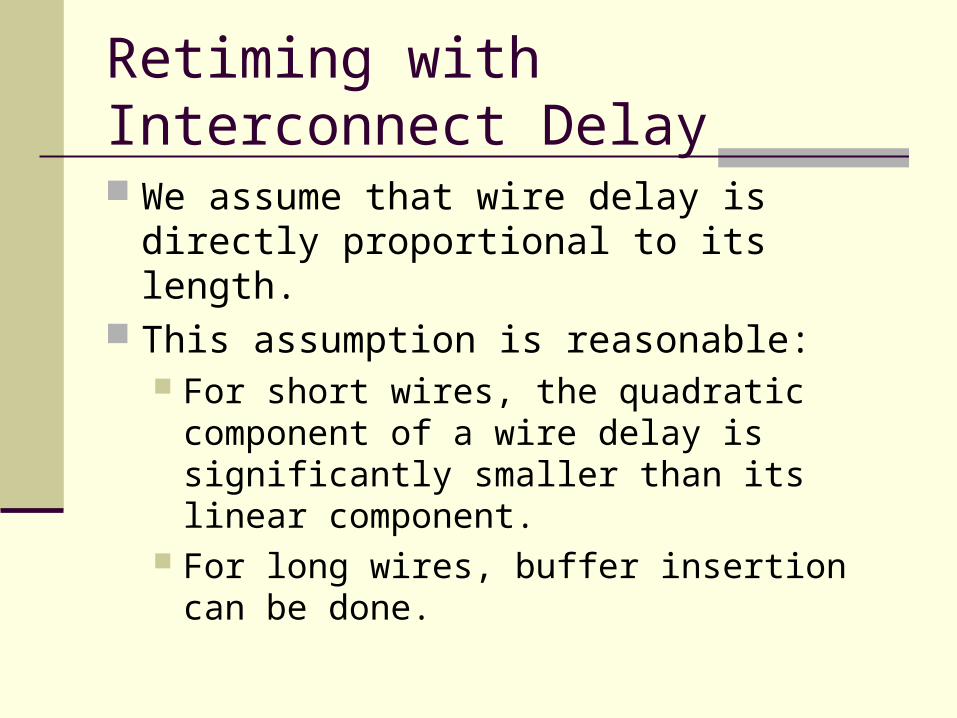
Retiming with Interconnect Delay
We assume that wire delay is directly proportional to its length.
This assumption is reasonable: For short wires, the quadratic component of a
wire delay is significantly smaller than its linear component.
For long wires, buffer insertion can be done.

Retiming with Interconnect Delay

Retiming with Interconnect Delay
Now, a retiming solution needs to specify: the retiming label r(v) for each node v. the positions of the registers on each edge.
The positions of the registerson the edges are important asthere are interconnect delay.
Retiming
r( ) = 0 r( ) = 0
r( ) = 0 r( ) = -1

Our Contributions
Optimal algorithm: O(|V||E| log |V| + |V|2 log2|V|) time per iteration.
Near-optimal algorithm: Only 0.13% larger than the optimal on average. O(|Vb||E| + |Vb||Eh|) time per iteration, e.g., a cir
cuit with 16.1K gates and 28.6K wires can be retimed in 44.32s by a 1.8GHz PIII PC.
Based on an optimal algorithm handling interconnect delay only, i.e., no gate delay.

Optimal Approach
Rewrite the ILP on p.8 as follows:
d(v) s(v) for all node v (1) s(v) c for all node v (2) r(u) r(v) w(e) for all edge e(u,v) (3) s(v) ≥ s(u) + d(e) + d(v) - c(r(v) - r(u) + w(e))
for all edge e(u,v) (4)

Optimal Approach
Similarly, write R(v) as r(v) + s(v)/c:
r(v) – R(v) -d(v)/c for all node v (1)
R(v) – r(v) 1 for all node v (2) r(u) r(v) w(e) for all edge e(u,v) (3) R(u) – R(v) w(e) - d(v)/c - d(e)/c for all edge e(u,v)
(4)
Again, the above set of constraints can be solved in polynomial time, though the runtime is quite long.

Optimal Approach
Circuit |V| |E| copt Runtime (s)
s1488 655 1405 18.85 5.62s1494 649 1411 20.78 4.37s3271 1574 2707 10.24 33.70s3330 1791 2890 27.05 43.14s3384 1687 2782 24.16 25.19s4863 2344 4093 23.58 87.75s5378 2781 4261 27.25 138.68s6669 3082 5399 22.96 177.59s9234 5599 8005 42.73 512.86
s13207 7953 11302 72.34 1161.07s15850 9774 13794 67.82 1545.59s35932 16067 28590 29.54 8644.27s38417 22181 32135 36.52 7680.79s38584 19255 33010 >15000

Near Optimal Approach
Transform the original graph G by splitting each node v (represents a gate) into a pair of nodes v1 and v2 connected by an edge with delay d(v).
v
v1
v2
delay = d(v)
delay = d(v)
delay = 0

Near Optimal Approach
After representing each gate by a wire, we can find an optimal retiming solution S for the transformed circuit G1. (We will show how to find the optimal solution with no gate delay.)
The clock period of S will be a lower bound L for the optimal solution Topt of G.
From S, we can obtain a feasible retiming solution for the original circuit G.

Near Optimal Approach
Registers retimed into a wire representing a gate v will be moved backward to the input edges or forward to the output edges depending on their distances from v1 and v2.
Linear programming is used to determine the positions of the registers on each edge after this relocation step to minimize the clock period considering both gate and wire delay.
v1
v2

Near Optimal Approach
It is now the problem of solving the retiming problem optimally assuming that gate delay is zero.
When there is no gate delay, the set of constraints on p.17 becomes:
r(v) – R(v) 0 for all node v (1) R(v) – r(v) 1 for all node v (2) r(u) r(v) w(e) for all edge e(u,v) (3) R(u) – R(v) w(e)-d(e)/c for all edge e(u,
v) (4)

Near Optimal Approach
Lemma 1: Given R(v) for all node v that satisfy constraint (4), we can obtain a solution to constraint (1)-(4) by setting
r(v) = trunc(R(v)) Given Lemma 1, we only need to solve constr
aint (4): R(u) – R(v) w(e)-d(e)/c for all edge e(u,v).
Consider the input graph G(V,E) such that the weight of each edge e(u,v) is -w(e)+d(e)/c.

Near Optimal Approach
There is a solution to constraint (4) iff G has no positive cycles.
Positive cycle detection in G can be achieved by positive cycle detection in a smaller graph H(Vb,Eh) constructed from G. This technique can be applied in other positive cycle detection problems, not necessarily in circuit retiming.
After solving R(v), we can find r(v) and s(v) for all node v.

Near Optimal Approach
After the binary search, we can find the optimal clock and the corresponding r(v) and s(v) for all node v. Then, we can place the registers accordingly:
u v
c
Other registers are placedright in front of v.
c - s(u)
Assume that r(v)-r(u)+w(e) = 4

Near Optimal Approach
First, assuming that gate delay is zero. Binary search to find the minimum feasible
clock period c To test the feasibility of a fixed c:
Transforming to a positive cycle detection problem on a reduced graph
Can be solved by a single-source longest-path algorithm

Results
Circuit copt Topt (s)
s1488 18.82 5.62s1494 20.78 4.37s3271 10.24 33.70s3330 27.05 43.14s3384 24.16 25.19s4863 23.58 87.75s5378 27.25 138.68s6669 22.96 177.59s9234 42.73 512.86
s13207 72.34 1161.07s15850 67.82 1545.59s35932 29.54 8644.27s38417 36.52 7680.79s38584 >15000
cnear opt
18.8520.7810.2427.0524.2123.5827.2723.0742.7372.3467.8229.5936.53
Tnear opt (s)
0.280.251.090.500.743.121.161.914.088.11
24.0261.2583.56
445.6394.26
Future Directions
Consider a more accurate modeling for the interconnect delay, e.g., use Elmore delay.
How to map the retiming solution to the floorplanning or placement solution? Registers are large and take up silicon resources.
How to consider fan-out capacitance with interconnect delay?