Embed Size (px)
Citation preview
VLSI ScalingMAH 1
Circuits and InterconnectsIn Aggressively Scaled CMOS
Mark HorowitzComputer Systems Laboratory
Stanford [email protected]
VLSI ScalingMAH 2
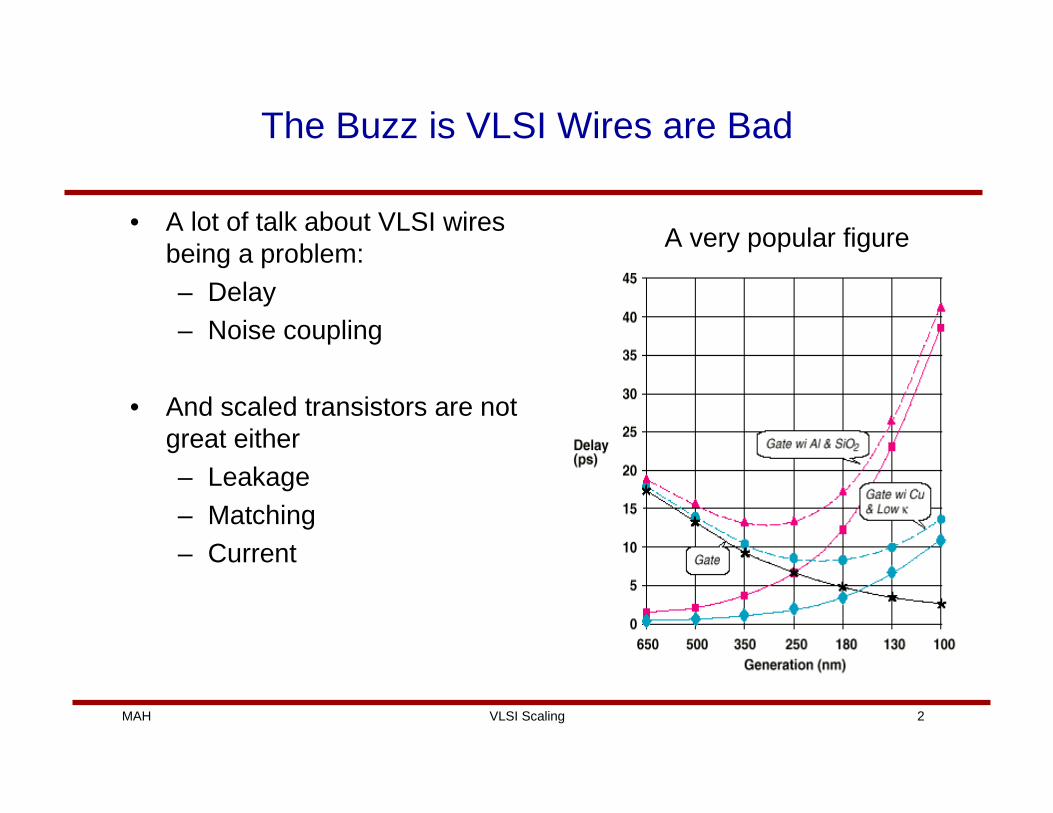
The Buzz is VLSI Wires are Bad
• A lot of talk about VLSI wires being a problem:– Delay– Noise coupling
• And scaled transistors are not great either– Leakage– Matching– Current
A very popular figure
VLSI ScalingMAH 3
How Will Scaling Change Design?
To answer this question:• First look at what changes when technology scales
– Surprisingly less changes than you might think– Components get faster (both wires and gates)– Mostly it allows one to build more complex devices
• Then look at how computing devices use silicon technology– How architects and circuit designers use the transistors– What are the looming problems with scaling– What can be done to help
• Let’s start by looking at scaling CMOS technology
VLSI ScalingMAH 4
Predicting the Future (without making a fool of yourself)
• Is very difficult– The only guarantee is:
The future will happen, and you will be wrong
• Two approaches– Think about limitations
• SIA 1994 Roadmap– Limited oxide thickness, small clock frequency growth, etc.– Industry hit points above the curve
– Project from current trends• SIA 1997 Roadmap
– Allow miracles to occur, continue trends– Project clock rates higher than physically possible
• So use a range of technology scalings– Better chance of covering the correct answer
VLSI ScalingMAH 5
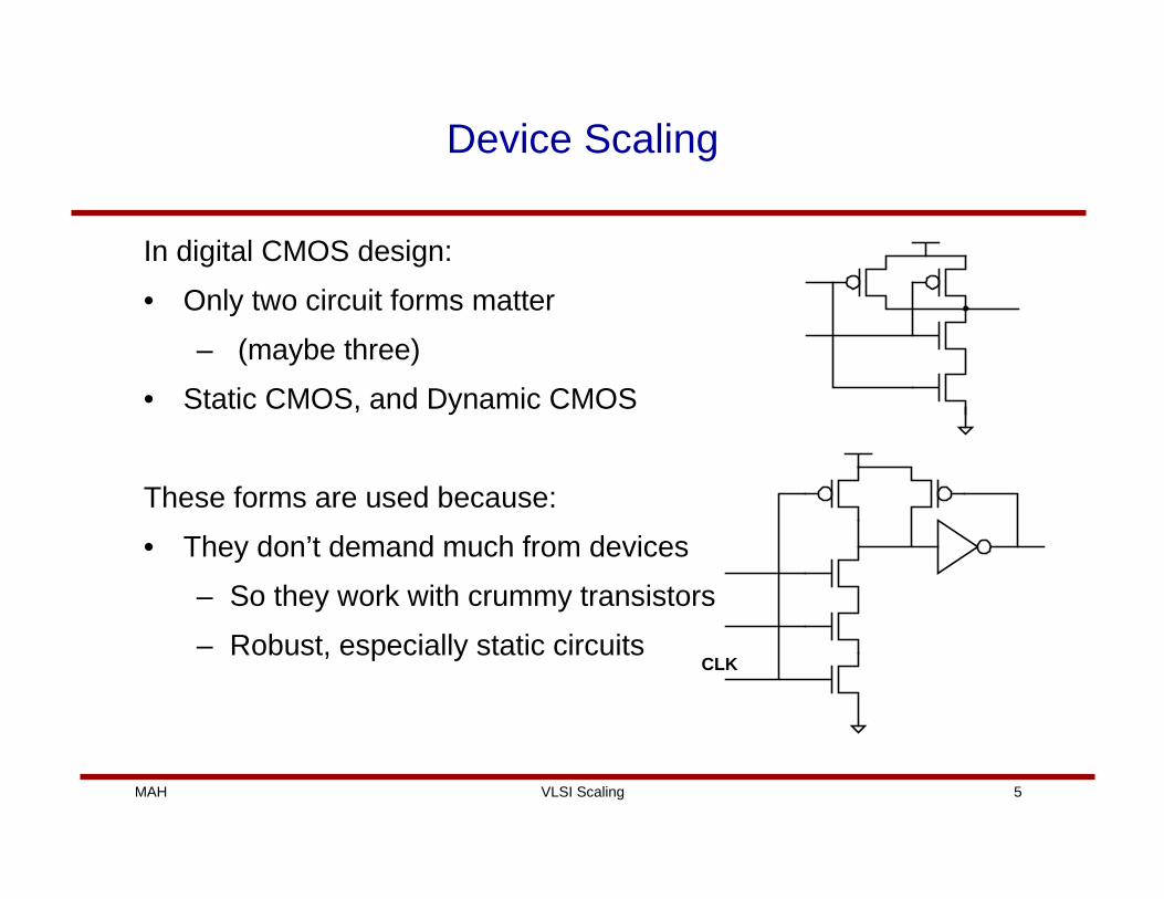
Device Scaling
In digital CMOS design:
• Only two circuit forms matter
– (maybe three)
• Static CMOS, and Dynamic CMOS
These forms are used because:
• They don’t demand much from devices
– So they work with crummy transistors
– Robust, especially static circuitsCLK
VLSI ScalingMAH 6
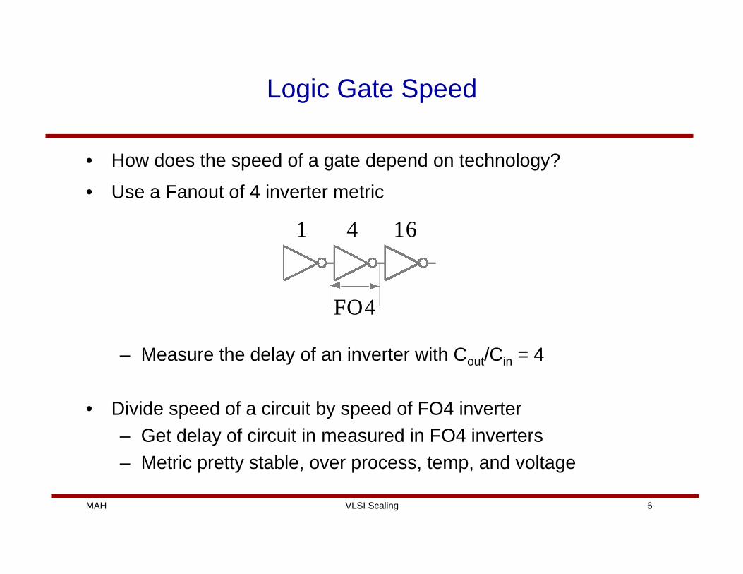
Logic Gate Speed
• How does the speed of a gate depend on technology?
• Use a Fanout of 4 inverter metric
– Measure the delay of an inverter with Cout/Cin = 4
• Divide speed of a circuit by speed of FO4 inverter– Get delay of circuit in measured in FO4 inverters– Metric pretty stable, over process, temp, and voltage
1 4 16
FO4
VLSI ScalingMAH 7
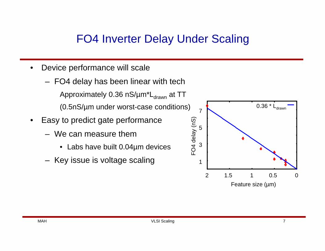
FO4 Inverter Delay Under Scaling
• Device performance will scale
– FO4 delay has been linear with tech
Approximately 0.36 nS/µm*Ldrawn at TT
(0.5nS/µm under worst-case conditions)
• Easy to predict gate performance
– We can measure them
• Labs have built 0.04µm devices
– Key issue is voltage scaling 1
3
5
7
00.511.52
FO
4 de
lay
(nS
)
Feature size (µm)
0.36 * Ldrawn
VLSI ScalingMAH 8
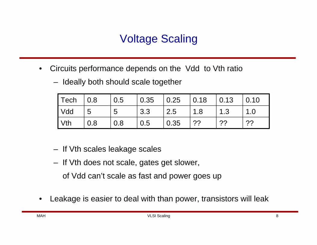
Voltage Scaling
• Circuits performance depends on the Vdd to Vth ratio
– Ideally both should scale together
– If Vth scales leakage scales
– If Vth does not scale, gates get slower,
of Vdd can’t scale as fast and power goes up
• Leakage is easier to deal with than power, transistors will leak
??
1.8
0.18
??
1.3
0.13
??
1.0
0.10
0.35
2.5
0.25
0.50.80.8Vth
3.355Vdd
0.350.50.8Tech
VLSI ScalingMAH 9
Circuit Power
• Is very much tied to voltage scaling
• If the power supply scales with technology
For a fixed complexity circuit
– Power scales down as α^3 if you run as same frequency
– Power scales down as α^2 if you run it 1/ α times faster
• Power scaling is a problem because
– Freq has been scaling at faster than 1/ α
– Complexity of machine has been growing
• This will continue to be an issue in future chips
• Remember scaling the technology makes a chip lower power!
VLSI ScalingMAH 10
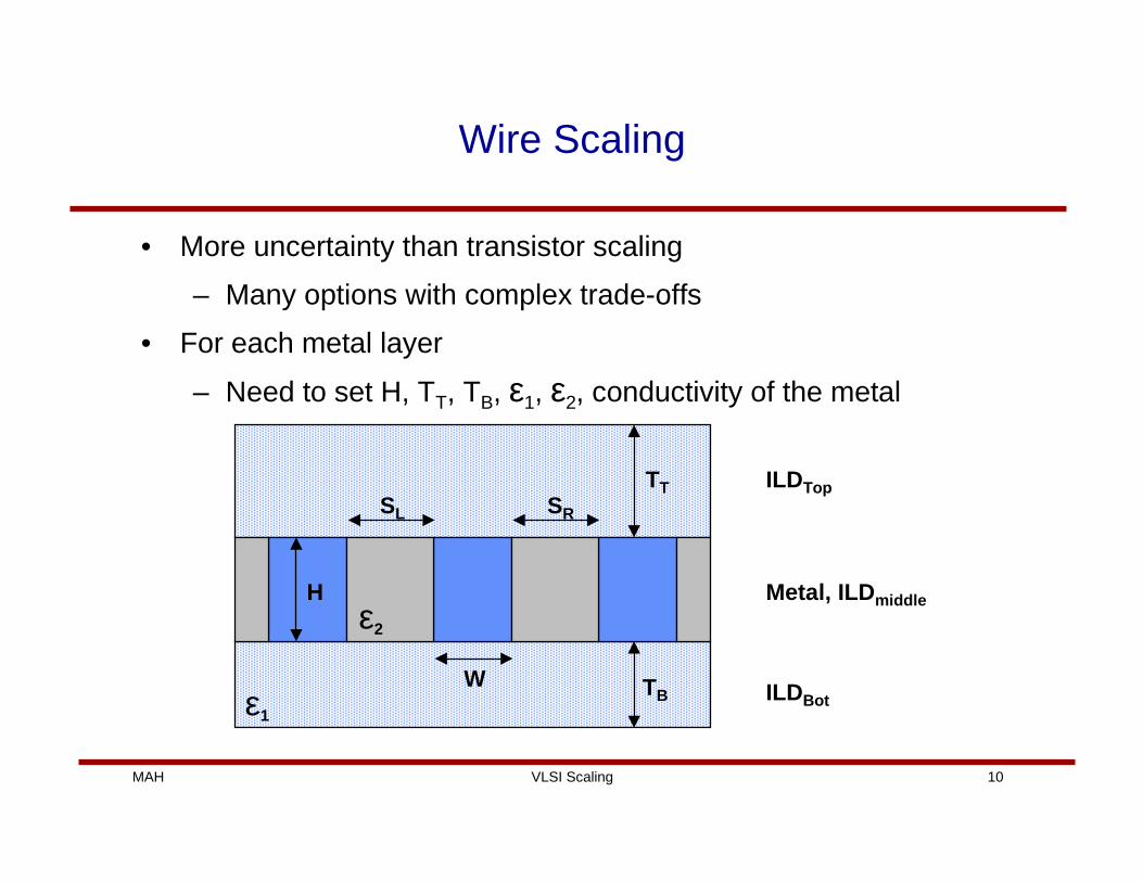
Wire Scaling
• More uncertainty than transistor scaling
– Many options with complex trade-offs
• For each metal layer
– Need to set H, TT, TB, ε1, ε2, conductivity of the metal
W
SRSL
TB
TT
H
ε1
ε2
ILDTop
ILDBot
Metal, ILDmiddle
VLSI ScalingMAH 11
0
0.2
0.4
0.6
0.25 0.18 0.13 0.1 0.07 0.05 0.035
pF
Technology Ldrawn (um)
Semi-global wire capacitance, 1mm long
Aggressive scalingConservative scaling
0
0.1
0.2
0.3
0.4
0.25 0.18 0.13 0.1 0.07 0.05 0.035
Ko
hm
s
Technology Ldrawn (um)
Semi-global wire resistance, 1mm long
Aggressive scalingConservative scaling
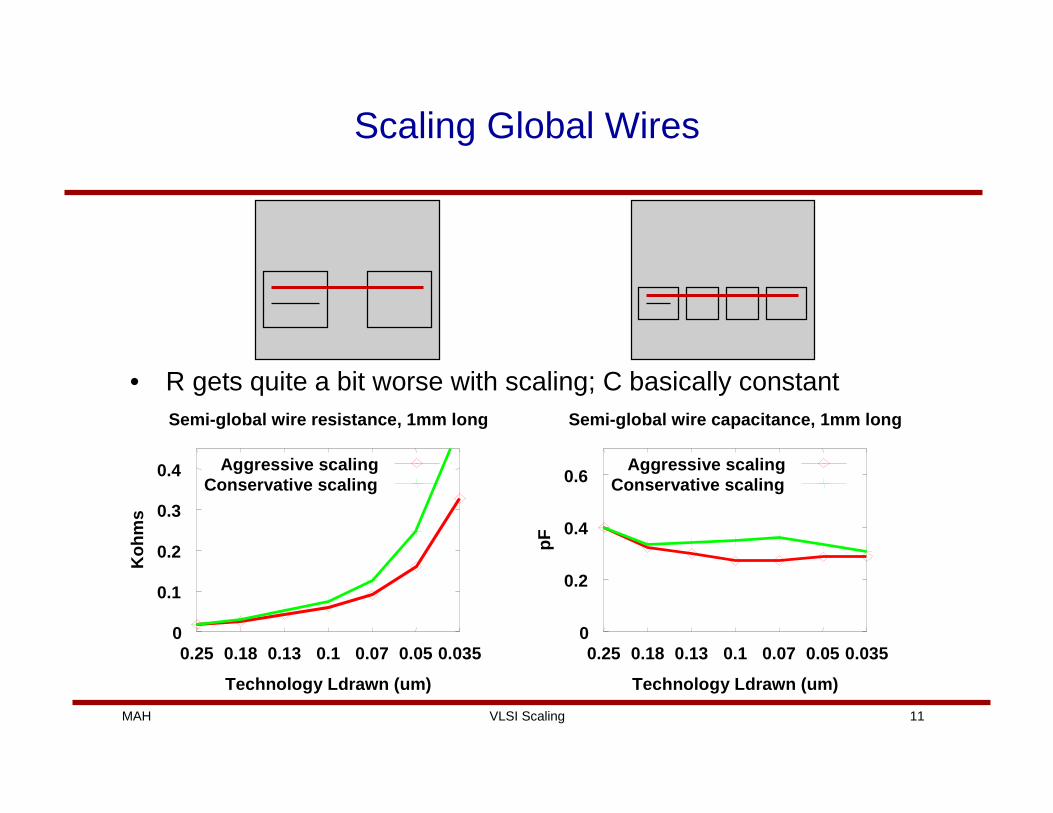
Scaling Global Wires
• R gets quite a bit worse with scaling; C basically constant
VLSI ScalingMAH 12
0
0.2
0.4
0.6
0.25 0.18 0.13 0.1 0.07 0.05 0.035
pF
Technology Ldrawn (um)
Semi-global wire capacitance, scaled length
Aggressive scalingConservative scaling
0
0.1
0.2
0.3
0.4
0.25 0.18 0.13 0.1 0.07 0.05 0.035
Ko
hm
s
Technology Ldrawn (um)
Semi-global wire resistance, scaled length
Aggressive scalingConservative scaling
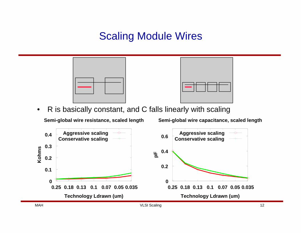
Scaling Module Wires
• R is basically constant, and C falls linearly with scaling
VLSI ScalingMAH 13
0
0.1
0.2
0.3
0.4
0.5
0.25 0.18 0.13 0.1 0.07 0.05 0.035
Wir
e d
elay
/Gat
e d
elay
Technology Ldrawn (um)
Semi-global wire, scaled length
Aggressive scalingConservative scaling
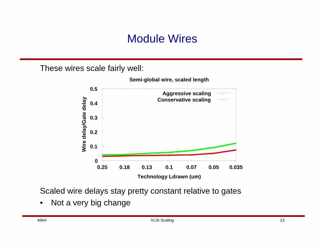
Scaled wire delays stay pretty constant relative to gates• Not a very big change
Module Wires
These wires scale fairly well:
VLSI ScalingMAH 14
0
1
2
3
4
5
6
7
0.25 0.18 0.13 0.1 0.07 0.05 0.035
Wir
e d
elay
/Gat
e d
elay
Technology Ldrawn (um)
Semi-global wire, 1mm long
Aggressive scalingConservative scaling
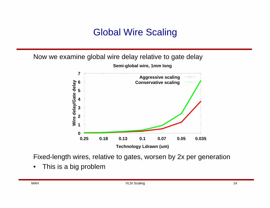
Global Wire Scaling
Fixed-length wires, relative to gates, worsen by 2x per generation• This is a big problem
Now we examine global wire delay relative to gate delay
VLSI ScalingMAH 15
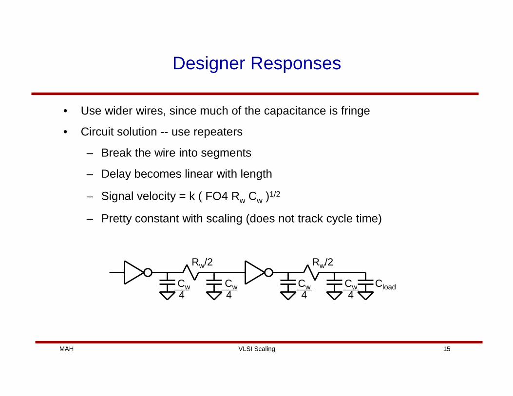
Designer Responses
• Use wider wires, since much of the capacitance is fringe
• Circuit solution -- use repeaters
– Break the wire into segments
– Delay becomes linear with length
– Signal velocity = k ( FO4 Rw Cw )1/2
– Pretty constant with scaling (does not track cycle time)
CloadCw4
Cw4
Rw/2
CloadCw4
Cw4
Rw/2
Cw4
Rw/2
Cw4
VLSI ScalingMAH 16
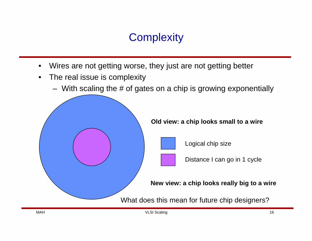
Complexity
• Wires are not getting worse, they just are not getting better• The real issue is complexity
– With scaling the # of gates on a chip is growing exponentially
Old view: a chip looks small to a wire
Logical chip size
Distance I can go in 1 cycle
New view: a chip looks really big to a wire
What does this mean for future chip designers?
VLSI ScalingMAH 17
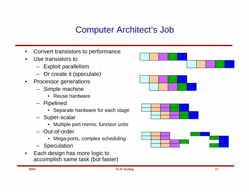
Computer Architect’s Job
• Convert transistors to performance• Use transistors to
– Exploit parallelism– Or create it (speculate)
• Processor generations– Simple machine
• Reuse hardware
– Pipelined• Separate hardware for each stage
– Super-scalar• Multiple port mems, function units
– Out-of-order• Mega-ports, complex scheduling
– Speculation• Each design has more logic to
accomplish same task (but faster)
VLSI ScalingMAH 18
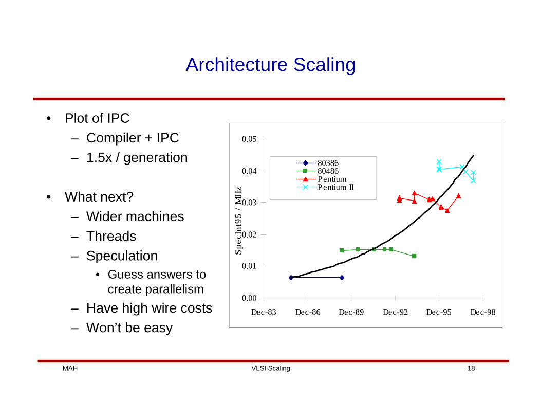
Architecture Scaling
• Plot of IPC– Compiler + IPC– 1.5x / generation
• What next?– Wider machines– Threads– Speculation
• Guess answers to create parallelism
– Have high wire costs– Won’t be easy
0.00
0.01
0.02
0.03
0.04
0.05
Dec-83 Dec-86 Dec-89 Dec-92 Dec-95 Dec-98
8038680486PentiumPentium II
Spe
cIn
t95
/ M
Hz
VLSI ScalingMAH 19
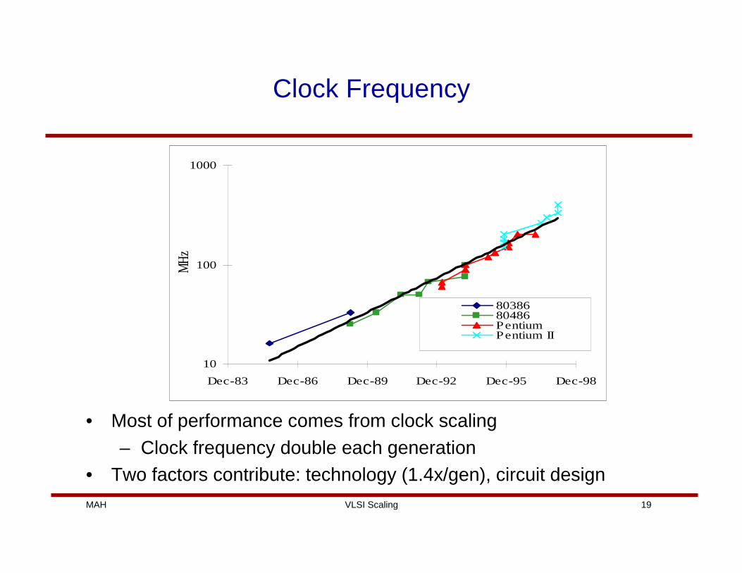
Clock Frequency
• Most of performance comes from clock scaling– Clock frequency double each generation
• Two factors contribute: technology (1.4x/gen), circuit design
10
100
1000
Dec-83 Dec-86 Dec-89 Dec-92 Dec-95 Dec-98
8038680486PentiumPentium II
MHz
VLSI ScalingMAH 20
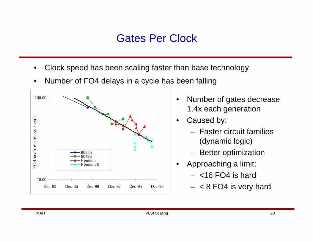
Gates Per Clock
• Clock speed has been scaling faster than base technology
• Number of FO4 delays in a cycle has been falling
• Number of gates decrease 1.4x each generation
• Caused by:– Faster circuit families
(dynamic logic)– Better optimization
• Approaching a limit:– <16 FO4 is hard– < 8 FO4 is very hard
10.00
100.00
Dec-83 Dec-86 Dec-89 Dec-92 Dec-95 Dec-98
8038680486PentiumPentium II
FO
4 in
vert
er d
elay
s /
cycl
e
VLSI ScalingMAH 21
Approaching a Discontinuity
Current GP architectures are not sustainable:
• Still based on the free communication model
– Maintaining a global shared resource model
– Large, complex communication needed
• Poor modularity
– Large design teams required
– Huge design and verification costs
VLSI ScalingMAH 22
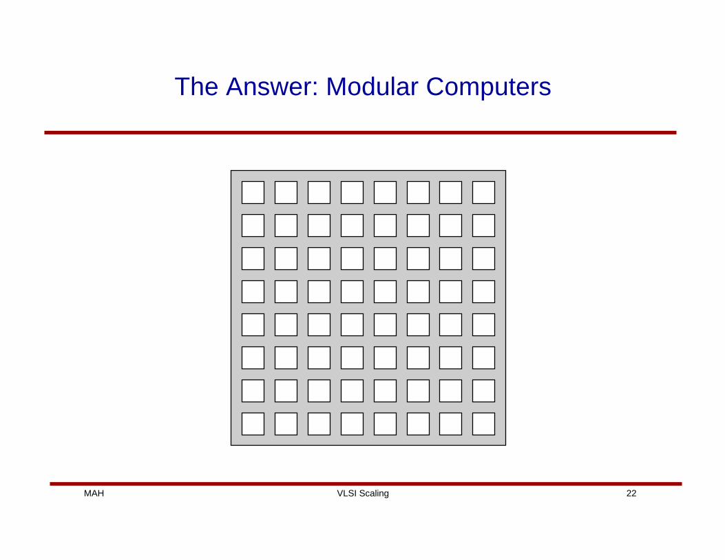
The Answer: Modular Computers
VLSI ScalingMAH 23
The Question:
How do you make a useful modular computer?
(Useful => Efficient -- cost, power)
VLSI ScalingMAH 24
Slow Process
Need to change the way people think at all levels
• Hardware design
– Function centric, write functions in Verilog
• Wires are implicit, through variables
• Programs are even worse
– All communication is through variables
– Memories are great communication boxes
• Any part of the program can read your output
• Algorithm design
– Today focus is on efficient computation
– Need to focus on efficient communication
VLSI ScalingMAH 25
Conclusions
At a module level, the wire problem is getting bigger (not harder)
• Back-end CAD tools need to deal with more and more wires
• Their capability to deal with long wires must improve
At a global level, the problem is worse
• The span of a cycle is a constant number of gates
– As chips grow in complexity, communication costs grow
• Designs (designers) must deal with these communication costs
– Free global resources don’t exist
– Need to design partitioned architectures for this new world