Embed Size (px)
Citation preview
CIS 501: Comp. Arch. | Prof. Milo Martin | ISAs & Single Cycle 1
CIS 371 Computer Organization and Design
Unit 4: Single-Cycle Datapath
Based on slides by Prof. Amir Roth & Prof. Milo Martin
CIS 501: Comp. Arch. | Prof. Milo Martin | ISAs & Single Cycle 2
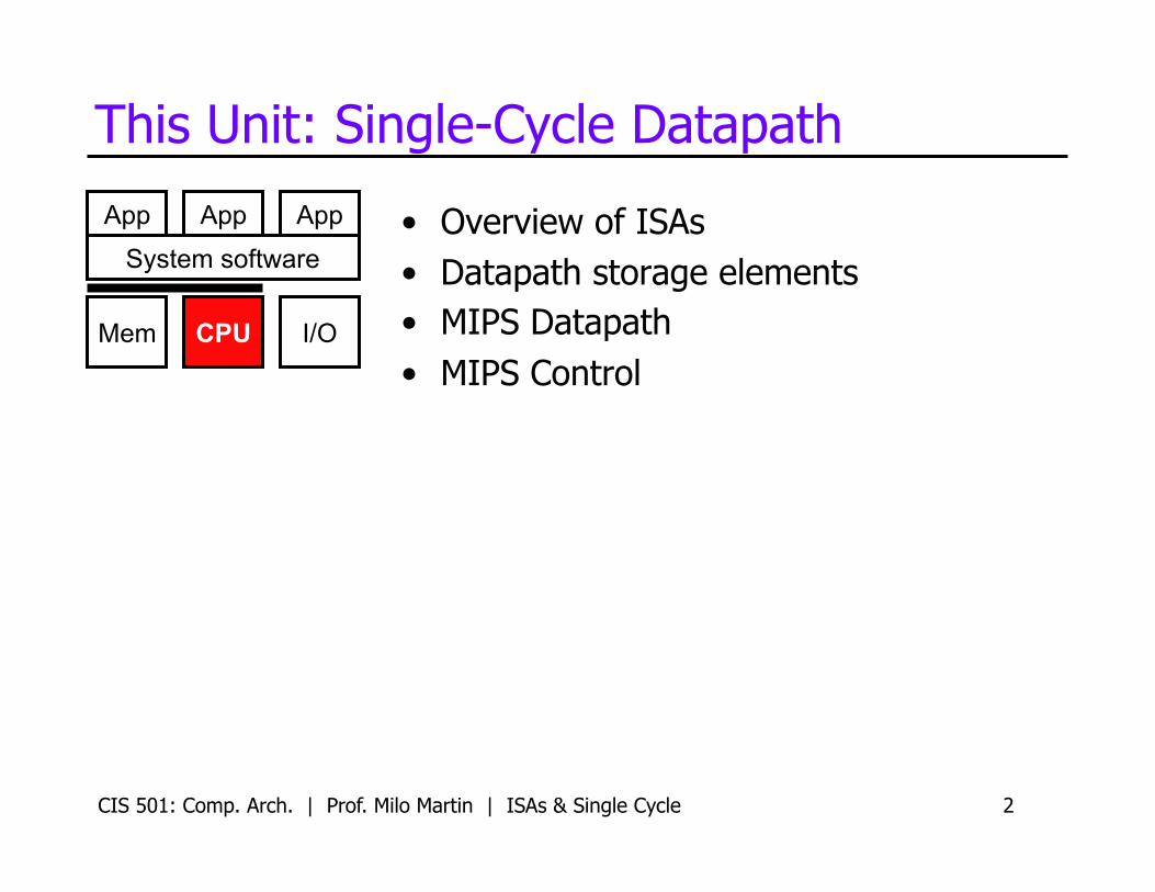
This Unit: Single-Cycle Datapath
• Overview of ISAs • Datapath storage elements • MIPS Datapath • MIPS Control
CPU Mem I/O
System software
App App App

CIS 501: Comp. Arch. | Prof. Milo Martin | ISAs & Single Cycle 3
Readings
• P&H • Sections 4.1 – 4.4
Recall from CIS240…
CIS 501: Comp. Arch. | Prof. Milo Martin | ISAs & Single Cycle 4
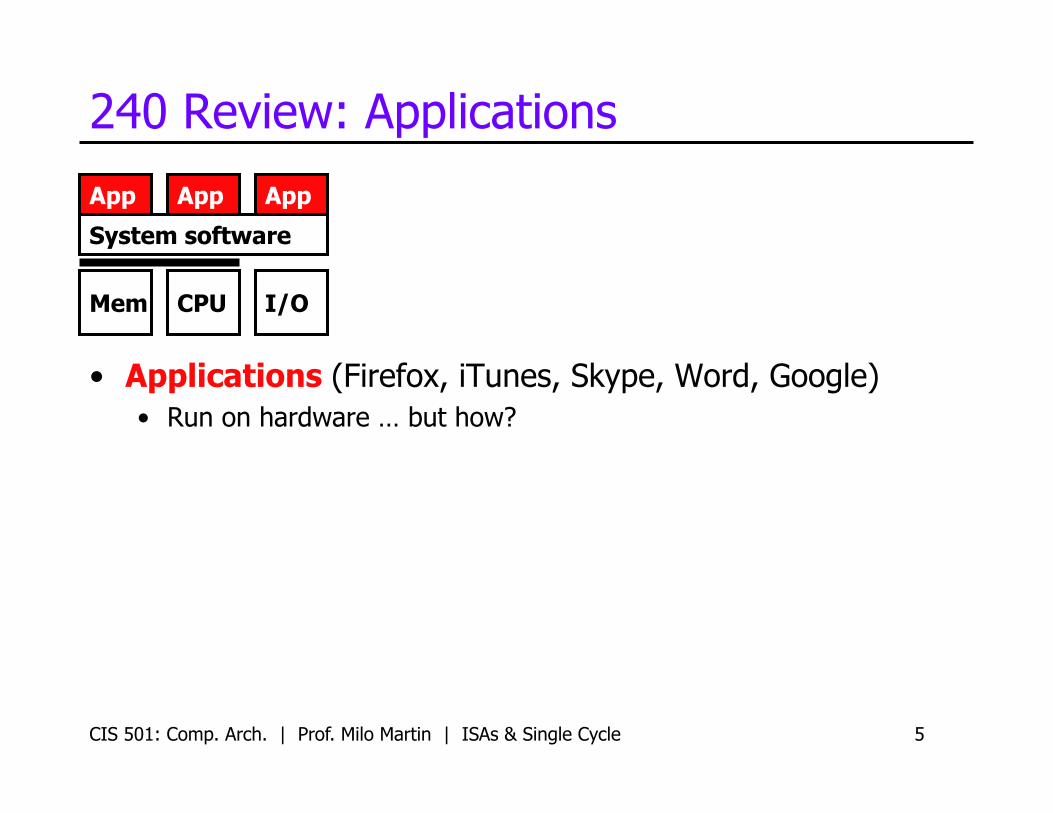
240 Review: Applications
• Applications (Firefox, iTunes, Skype, Word, Google) • Run on hardware … but how?
CIS 501: Comp. Arch. | Prof. Milo Martin | ISAs & Single Cycle 5
CPU Mem I/O
System software
App App App
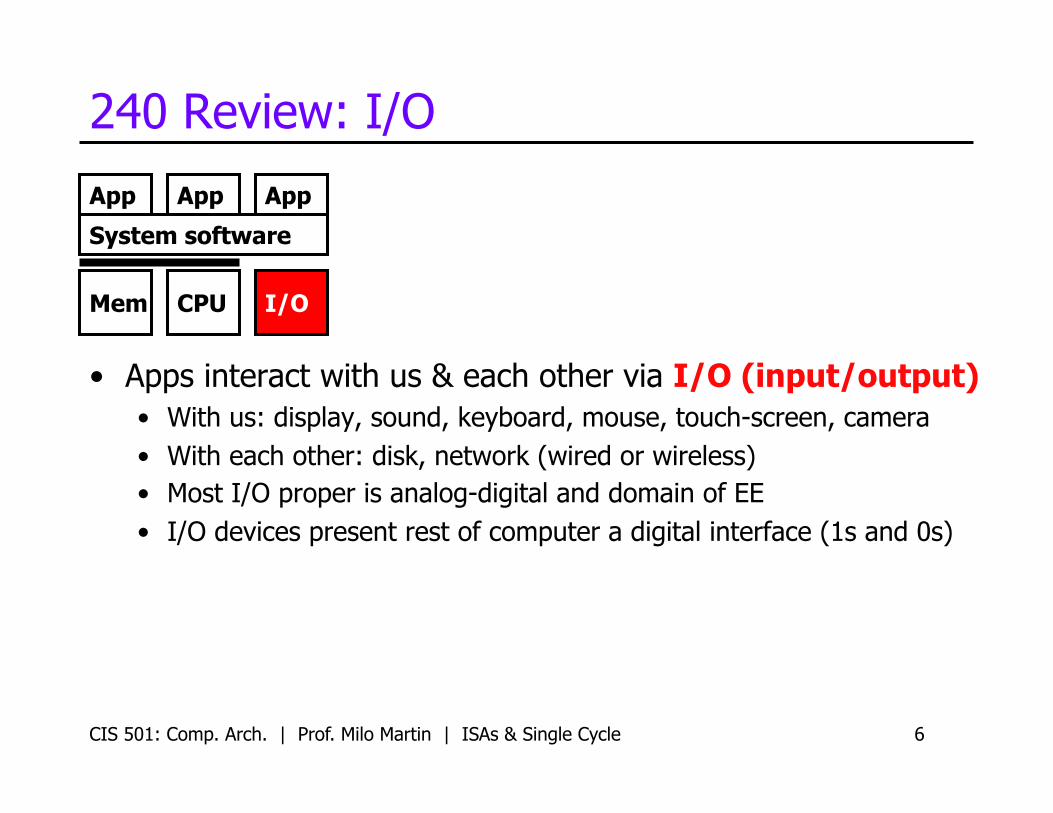
240 Review: I/O
• Apps interact with us & each other via I/O (input/output) • With us: display, sound, keyboard, mouse, touch-screen, camera • With each other: disk, network (wired or wireless) • Most I/O proper is analog-digital and domain of EE • I/O devices present rest of computer a digital interface (1s and 0s)
CIS 501: Comp. Arch. | Prof. Milo Martin | ISAs & Single Cycle 6
CPU Mem I/O
System software
App App App
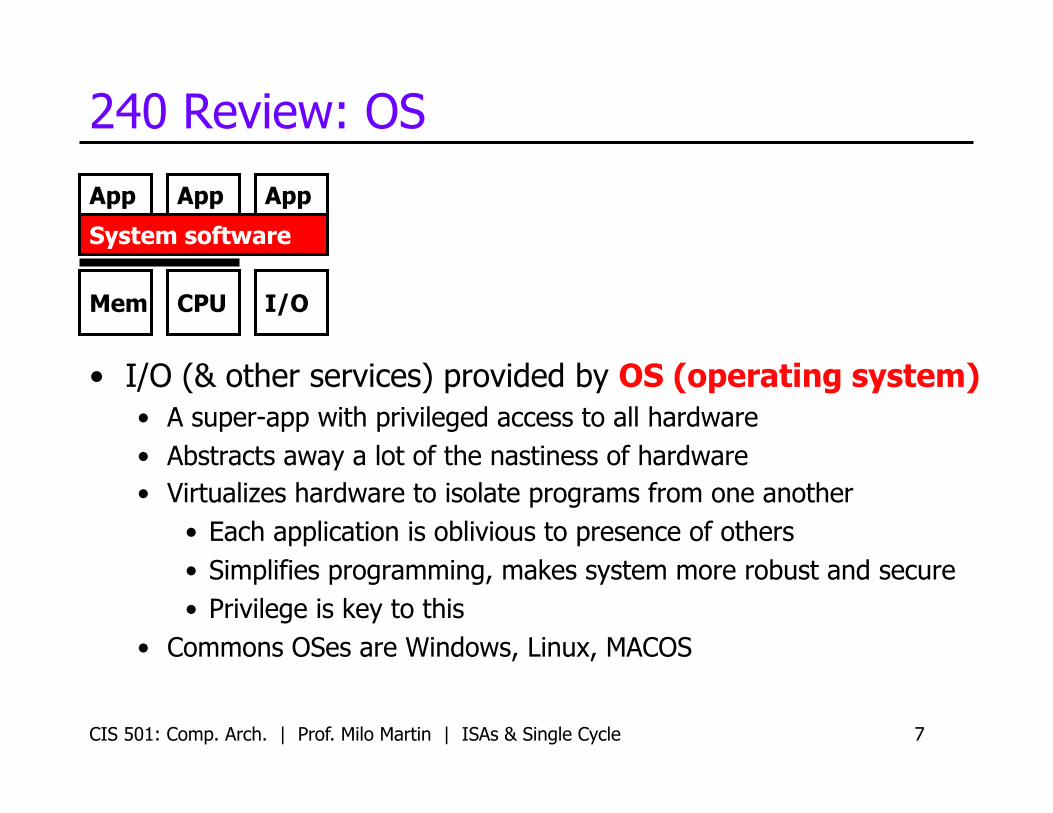
240 Review: OS
• I/O (& other services) provided by OS (operating system) • A super-app with privileged access to all hardware • Abstracts away a lot of the nastiness of hardware • Virtualizes hardware to isolate programs from one another
• Each application is oblivious to presence of others • Simplifies programming, makes system more robust and secure • Privilege is key to this
• Commons OSes are Windows, Linux, MACOS
CIS 501: Comp. Arch. | Prof. Milo Martin | ISAs & Single Cycle 7
CPU Mem I/O
System software
App App App
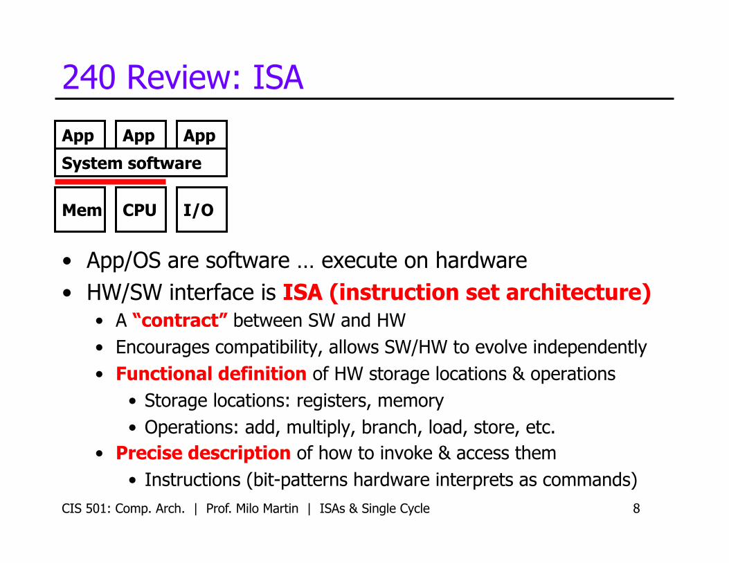
240 Review: ISA
• App/OS are software … execute on hardware • HW/SW interface is ISA (instruction set architecture)
• A “contract” between SW and HW • Encourages compatibility, allows SW/HW to evolve independently • Functional definition of HW storage locations & operations
• Storage locations: registers, memory • Operations: add, multiply, branch, load, store, etc.
• Precise description of how to invoke & access them • Instructions (bit-patterns hardware interprets as commands)
CIS 501: Comp. Arch. | Prof. Milo Martin | ISAs & Single Cycle 8
CPU Mem I/O
System software
App App App

240 Review: LC4 ISA
• LC4: a toy ISA you know • 16-bit ISA (what does this mean?) • 16-bit insns • 8 registers (integer) • ~30 different insns • Simple OS support
• Assembly language • Human-readable ISA representation
CIS 501: Comp. Arch. | Prof. Milo Martin | ISAs & Single Cycle 9
CPU Mem I/O
System software
App App App
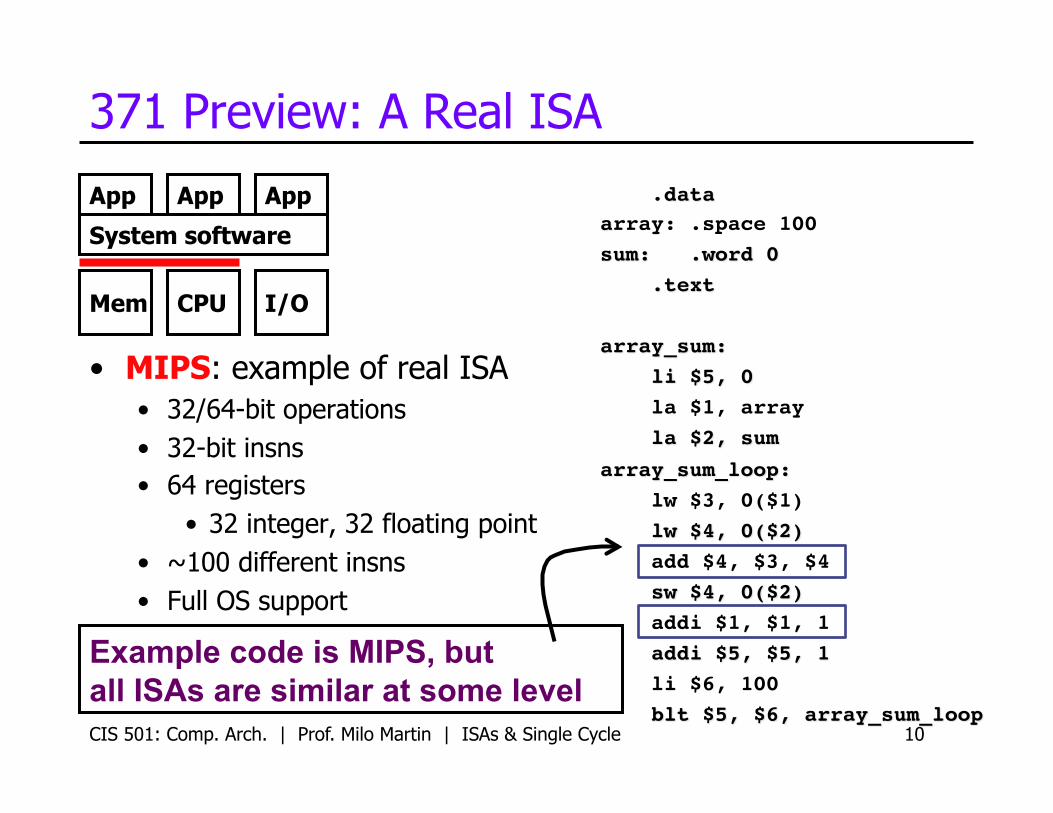
371 Preview: A Real ISA
• MIPS: example of real ISA • 32/64-bit operations • 32-bit insns • 64 registers
• 32 integer, 32 floating point • ~100 different insns • Full OS support
CIS 501: Comp. Arch. | Prof. Milo Martin | ISAs & Single Cycle 10
CPU Mem I/O
System software
App App App
Example code is MIPS, but all ISAs are similar at some level
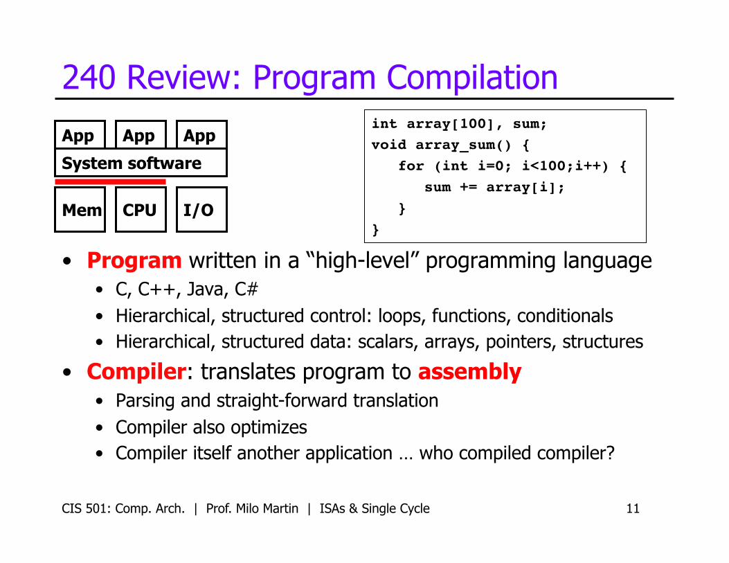
240 Review: Program Compilation
• Program written in a “high-level” programming language • C, C++, Java, C# • Hierarchical, structured control: loops, functions, conditionals • Hierarchical, structured data: scalars, arrays, pointers, structures
• Compiler: translates program to assembly • Parsing and straight-forward translation • Compiler also optimizes • Compiler itself another application … who compiled compiler?
CIS 501: Comp. Arch. | Prof. Milo Martin | ISAs & Single Cycle 11
CPU Mem I/O
System software
App App App int array[100], sum;!void array_sum() {! for (int i=0; i<100;i++) {! sum += array[i];! }!}!
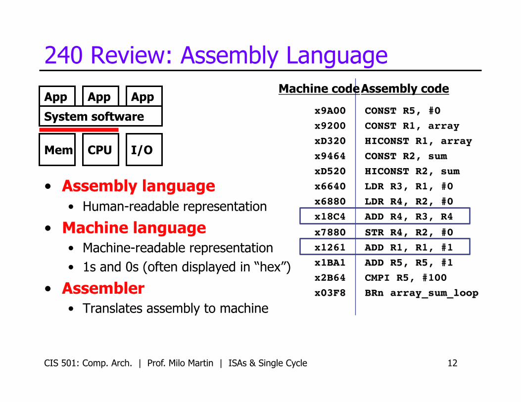
240 Review: Assembly Language
• Assembly language • Human-readable representation
• Machine language • Machine-readable representation • 1s and 0s (often displayed in “hex”)
• Assembler • Translates assembly to machine
CIS 501: Comp. Arch. | Prof. Milo Martin | ISAs & Single Cycle 12
CPU Mem I/O
System software
App App App Machine code Assembly code
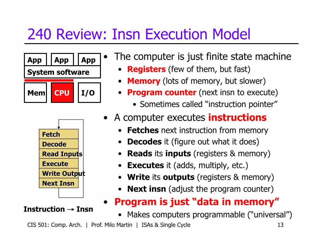
240 Review: Insn Execution Model • The computer is just finite state machine
• Registers (few of them, but fast) • Memory (lots of memory, but slower) • Program counter (next insn to execute)
• Sometimes called “instruction pointer”
• A computer executes instructions • Fetches next instruction from memory • Decodes it (figure out what it does) • Reads its inputs (registers & memory) • Executes it (adds, multiply, etc.) • Write its outputs (registers & memory) • Next insn (adjust the program counter)
• Program is just “data in memory” • Makes computers programmable (“universal”)
CIS 501: Comp. Arch. | Prof. Milo Martin | ISAs & Single Cycle 13
CPU Mem I/O
System software
App App App
Instruction → Insn

Role of the Compiler
CIS 501: Comp. Arch. | Prof. Milo Martin | ISAs & Single Cycle 14
CIS 501: Comp. Arch. | Prof. Milo Martin | ISAs & Single Cycle 15
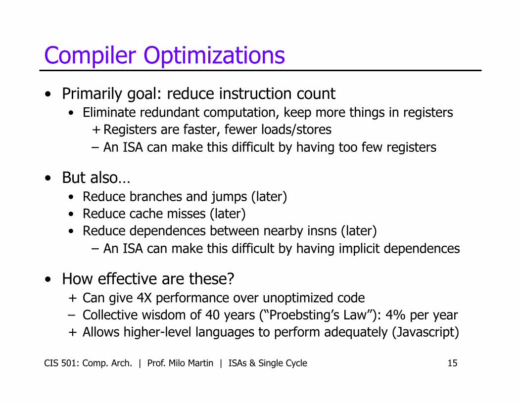
Compiler Optimizations • Primarily goal: reduce instruction count
• Eliminate redundant computation, keep more things in registers + Registers are faster, fewer loads/stores – An ISA can make this difficult by having too few registers
• But also… • Reduce branches and jumps (later) • Reduce cache misses (later) • Reduce dependences between nearby insns (later)
– An ISA can make this difficult by having implicit dependences
• How effective are these? + Can give 4X performance over unoptimized code – Collective wisdom of 40 years (“Proebsting’s Law”): 4% per year + Allows higher-level languages to perform adequately (Javascript)
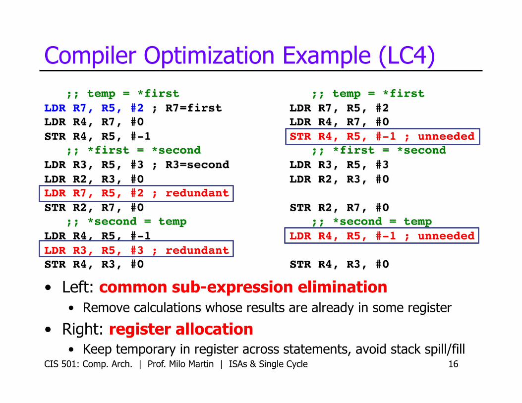
Compiler Optimization Example (LC4)
• Left: common sub-expression elimination • Remove calculations whose results are already in some register
• Right: register allocation • Keep temporary in register across statements, avoid stack spill/fill
CIS 501: Comp. Arch. | Prof. Milo Martin | ISAs & Single Cycle 16
What is an ISA?
CIS 501: Comp. Arch. | Prof. Milo Martin | ISAs & Single Cycle 17
CIS 501: Comp. Arch. | Prof. Milo Martin | ISAs & Single Cycle 18
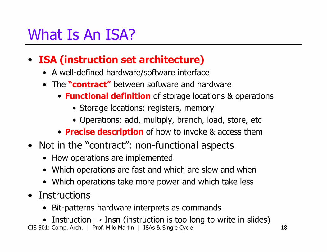
What Is An ISA?
• ISA (instruction set architecture) • A well-defined hardware/software interface • The “contract” between software and hardware
• Functional definition of storage locations & operations • Storage locations: registers, memory • Operations: add, multiply, branch, load, store, etc
• Precise description of how to invoke & access them
• Not in the “contract”: non-functional aspects • How operations are implemented • Which operations are fast and which are slow and when • Which operations take more power and which take less
• Instructions • Bit-patterns hardware interprets as commands • Instruction → Insn (instruction is too long to write in slides)
CIS 501: Comp. Arch. | Prof. Milo Martin | ISAs & Single Cycle 19
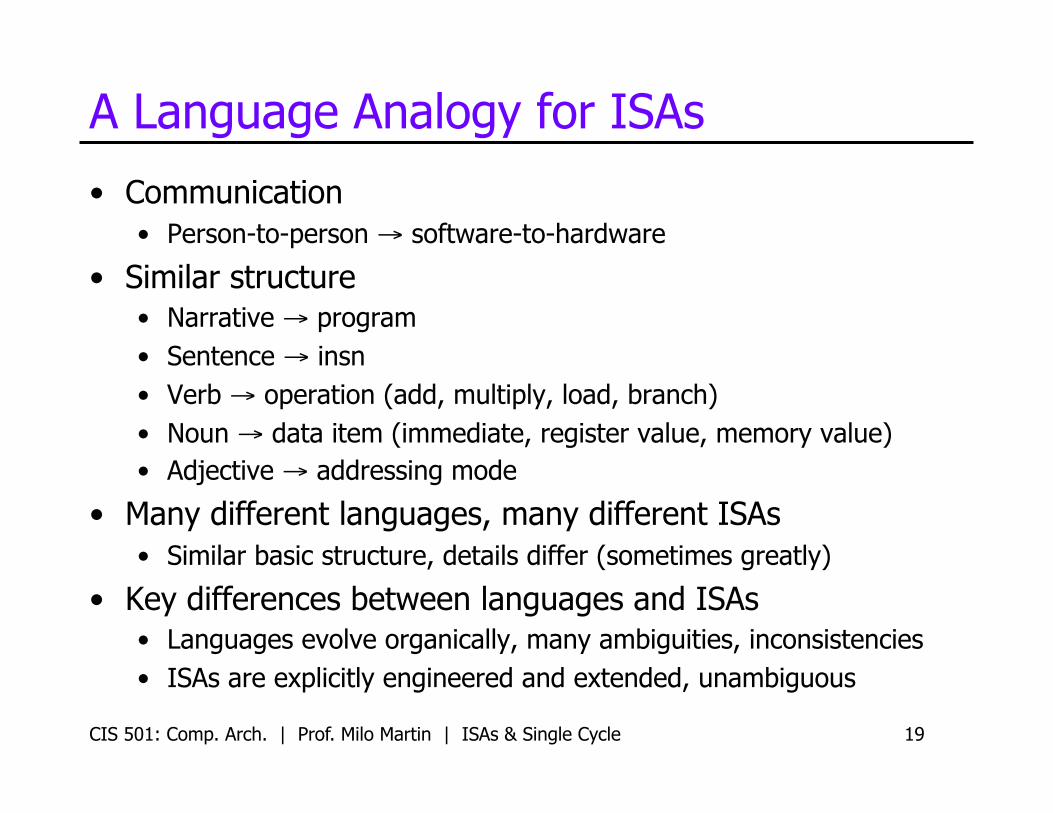
A Language Analogy for ISAs
• Communication • Person-to-person → software-to-hardware
• Similar structure • Narrative → program • Sentence → insn • Verb → operation (add, multiply, load, branch) • Noun → data item (immediate, register value, memory value) • Adjective → addressing mode
• Many different languages, many different ISAs • Similar basic structure, details differ (sometimes greatly)
• Key differences between languages and ISAs • Languages evolve organically, many ambiguities, inconsistencies • ISAs are explicitly engineered and extended, unambiguous
CIS 501: Comp. Arch. | Prof. Milo Martin | ISAs & Single Cycle 20
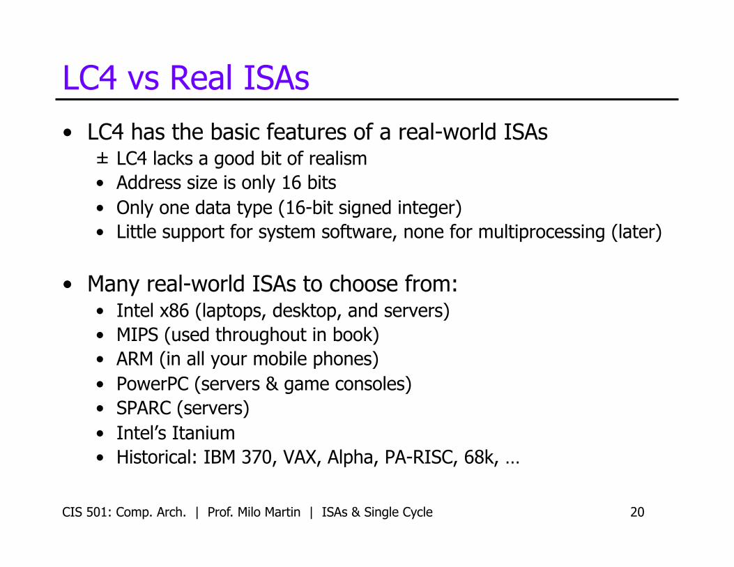
LC4 vs Real ISAs • LC4 has the basic features of a real-world ISAs
± LC4 lacks a good bit of realism • Address size is only 16 bits • Only one data type (16-bit signed integer) • Little support for system software, none for multiprocessing (later)
• Many real-world ISAs to choose from: • Intel x86 (laptops, desktop, and servers) • MIPS (used throughout in book) • ARM (in all your mobile phones) • PowerPC (servers & game consoles) • SPARC (servers) • Intel’s Itanium • Historical: IBM 370, VAX, Alpha, PA-RISC, 68k, …
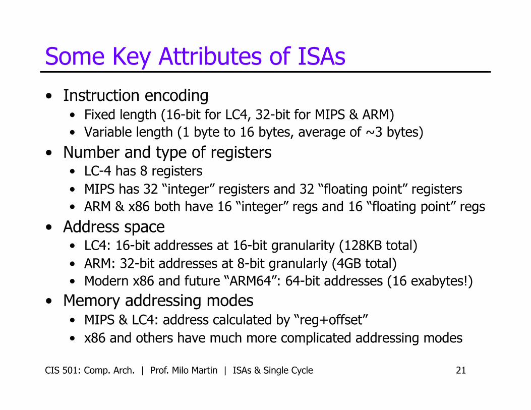
Some Key Attributes of ISAs • Instruction encoding
• Fixed length (16-bit for LC4, 32-bit for MIPS & ARM) • Variable length (1 byte to 16 bytes, average of ~3 bytes)
• Number and type of registers • LC-4 has 8 registers • MIPS has 32 “integer” registers and 32 “floating point” registers • ARM & x86 both have 16 “integer” regs and 16 “floating point” regs
• Address space • LC4: 16-bit addresses at 16-bit granularity (128KB total) • ARM: 32-bit addresses at 8-bit granularly (4GB total) • Modern x86 and future “ARM64”: 64-bit addresses (16 exabytes!)
• Memory addressing modes • MIPS & LC4: address calculated by “reg+offset” • x86 and others have much more complicated addressing modes
CIS 501: Comp. Arch. | Prof. Milo Martin | ISAs & Single Cycle 21

ISA Code Examples
CIS 501: Comp. Arch. | Prof. Milo Martin | ISAs & Single Cycle 22
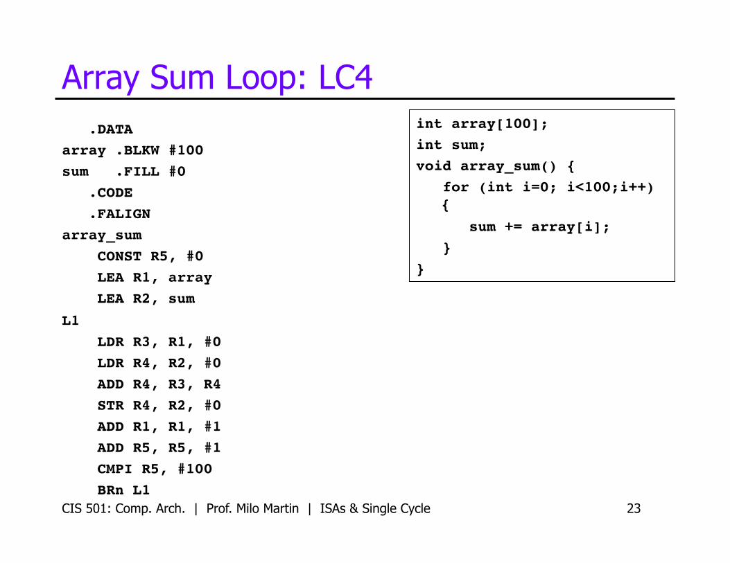
Array Sum Loop: LC4
CIS 501: Comp. Arch. | Prof. Milo Martin | ISAs & Single Cycle 23
.DATA!array .BLKW #100!sum .FILL #0! .CODE! .FALIGN!array_sum! CONST R5, #0! LEA R1, array! LEA R2, sum!
L1! LDR R3, R1, #0! LDR R4, R2, #0! ADD R4, R3, R4! STR R4, R2, #0! ADD R1, R1, #1! ADD R5, R5, #1! CMPI R5, #100! BRn L1!
int array[100];!int sum;!void array_sum() {! for (int i=0; i<100;i++)
{!
sum += array[i];! }!}!
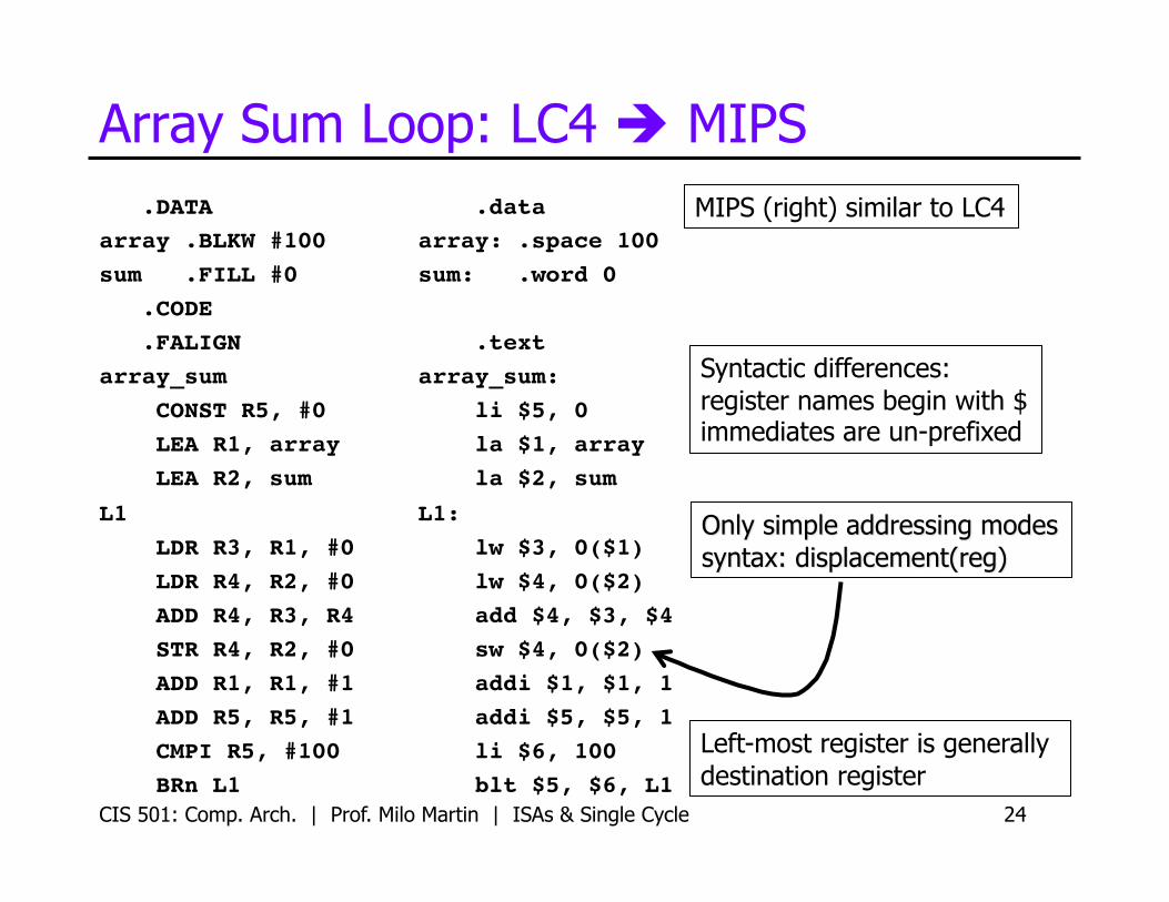
Array Sum Loop: LC4 MIPS
CIS 501: Comp. Arch. | Prof. Milo Martin | ISAs & Single Cycle 24
.DATA!array .BLKW #100!sum .FILL #0! .CODE! .FALIGN!array_sum! CONST R5, #0! LEA R1, array! LEA R2, sum!
L1! LDR R3, R1, #0! LDR R4, R2, #0! ADD R4, R3, R4! STR R4, R2, #0! ADD R1, R1, #1! ADD R5, R5, #1! CMPI R5, #100! BRn L1!
.data!array: .space 100!sum: .word 0!
.text!array_sum:! li $5, 0! la $1, array! la $2, sum!
L1:! lw $3, 0($1)! lw $4, 0($2)! add $4, $3, $4! sw $4, 0($2)! addi $1, $1, 1! addi $5, $5, 1! li $6, 100! blt $5, $6, L1!
Syntactic differences: register names begin with $ immediates are un-prefixed
MIPS (right) similar to LC4
Left-most register is generally destination register
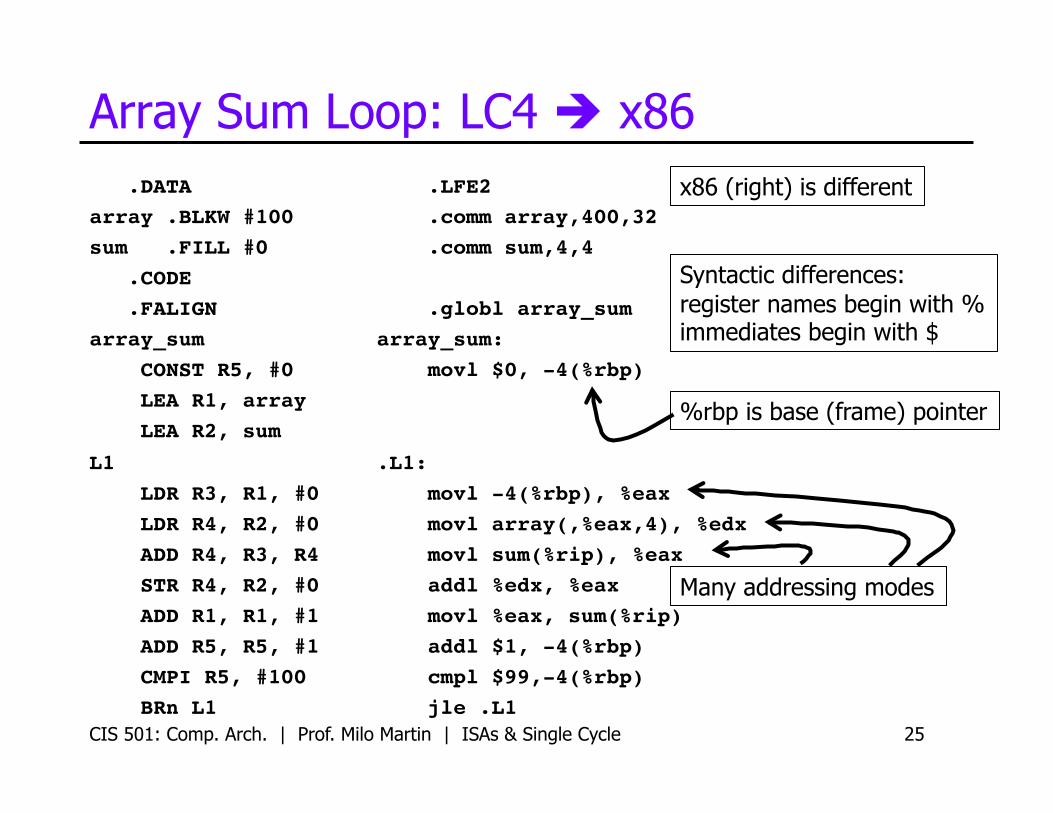
Array Sum Loop: LC4 x86
CIS 501: Comp. Arch. | Prof. Milo Martin | ISAs & Single Cycle 25
.DATA!array .BLKW #100!sum .FILL #0! .CODE! .FALIGN!array_sum! CONST R5, #0! LEA R1, array! LEA R2, sum!
L1! LDR R3, R1, #0! LDR R4, R2, #0! ADD R4, R3, R4! STR R4, R2, #0! ADD R1, R1, #1! ADD R5, R5, #1! CMPI R5, #100! BRn L1!
.LFE2! .comm array,400,32! .comm sum,4,4!
.globl array_sum!array_sum:! movl $0, -4(%rbp)!
.L1:! movl -4(%rbp), %eax! movl array(,%eax,4), %edx! movl sum(%rip), %eax ! addl %edx, %eax! movl %eax, sum(%rip)! addl $1, -4(%rbp)! cmpl $99,-4(%rbp)! jle .L1!
x86 (right) is different
Syntactic differences: register names begin with % immediates begin with $
%rbp is base (frame) pointer
Many addressing modes
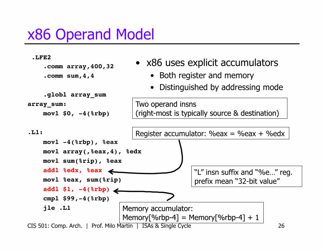
x86 Operand Model
• x86 uses explicit accumulators • Both register and memory • Distinguished by addressing mode
CIS 501: Comp. Arch. | Prof. Milo Martin | ISAs & Single Cycle 26
Register accumulator: %eax = %eax + %edx
“L” insn suffix and “%e…” reg. prefix mean “32-bit value”
Implementing an ISA
CIS 501: Comp. Arch. | Prof. Milo Martin | ISAs & Single Cycle 27
CIS 501: Comp. Arch. | Prof. Milo Martin | ISAs & Single Cycle 28
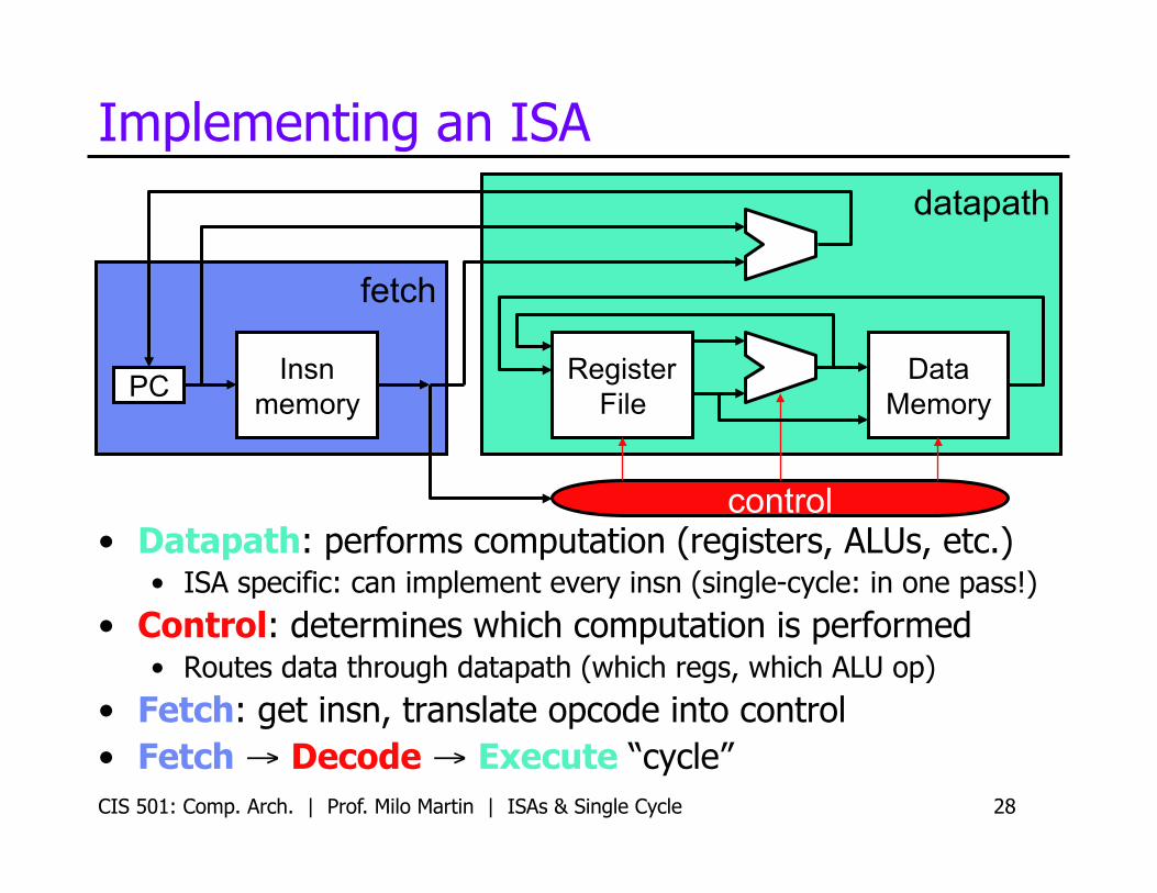
Implementing an ISA
• Datapath: performs computation (registers, ALUs, etc.) • ISA specific: can implement every insn (single-cycle: in one pass!)
• Control: determines which computation is performed • Routes data through datapath (which regs, which ALU op)
• Fetch: get insn, translate opcode into control • Fetch → Decode → Execute “cycle”
PC Insn
memory Register
File Data
Memory
control
datapath
fetch
CIS 501: Comp. Arch. | Prof. Milo Martin | ISAs & Single Cycle 29
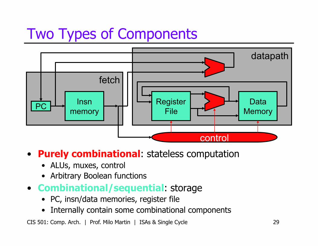
Two Types of Components
• Purely combinational: stateless computation • ALUs, muxes, control • Arbitrary Boolean functions
• Combinational/sequential: storage • PC, insn/data memories, register file • Internally contain some combinational components
PC Insn
memory Register
File Data
Memory
control
datapath
fetch
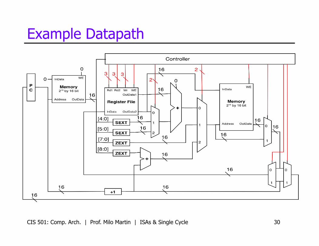
Example Datapath
CIS 501: Comp. Arch. | Prof. Milo Martin | ISAs & Single Cycle 30
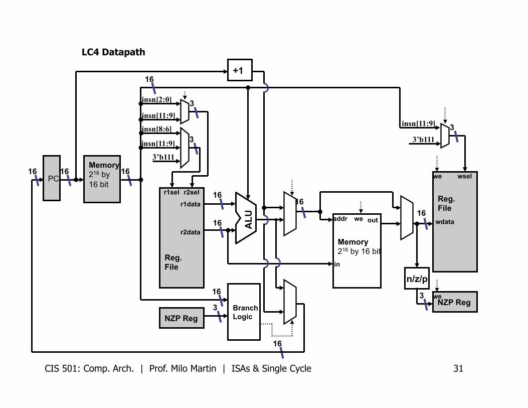
PC
Memory 216 by 16 bit
16 16
16
3’b111
insn[11:9] 3
Branch Logic
16
16
LC4 Datapath
Reg. File
wdata
3’b111
insn[11:9] 3
insn[11:9]
insn[2:0] 3
Reg. File
r1sel r2sel
r1data
r2data
wsel we
NZP Reg we
NZP Reg 3
16
16
16
Memory 216 by 16 bit
in
outaddr we
16
n/z/p
3
insn[8:6]
16
ALU
+1
31 CIS 501: Comp. Arch. | Prof. Milo Martin | ISAs & Single Cycle
MIPS Datapath
CIS 501: Comp. Arch. | Prof. Milo Martin | ISAs & Single Cycle 32
CIS 501: Comp. Arch. | Prof. Milo Martin | ISAs & Single Cycle 33
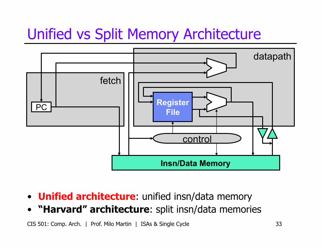
Unified vs Split Memory Architecture
• Unified architecture: unified insn/data memory • “Harvard” architecture: split insn/data memories
PC Register
File
Insn/Data Memory
control
datapath
fetch
CIS 501: Comp. Arch. | Prof. Milo Martin | ISAs & Single Cycle 34
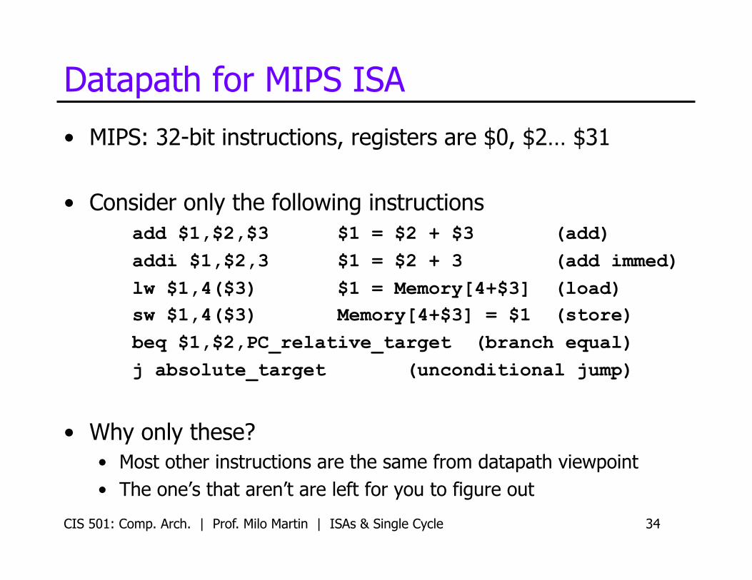
Datapath for MIPS ISA
• MIPS: 32-bit instructions, registers are $0, $2… $31
• Consider only the following instructions add $1,$2,$3 $1 = $2 + $3 (add) addi $1,$2,3 $1 = $2 + 3 (add immed) lw $1,4($3) $1 = Memory[4+$3] (load) sw $1,4($3) Memory[4+$3] = $1 (store) beq $1,$2,PC_relative_target (branch equal) j absolute_target (unconditional jump)
• Why only these? • Most other instructions are the same from datapath viewpoint • The one’s that aren’t are left for you to figure out
CIS 501: Comp. Arch. | Prof. Milo Martin | ISAs & Single Cycle 35
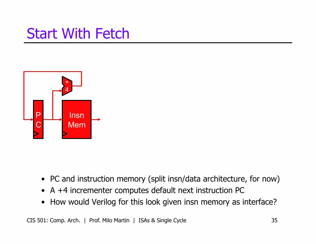
Start With Fetch
• PC and instruction memory (split insn/data architecture, for now) • A +4 incrementer computes default next instruction PC • How would Verilog for this look given insn memory as interface?
P C
Insn Mem
+ 4
CIS 501: Comp. Arch. | Prof. Milo Martin | ISAs & Single Cycle 36
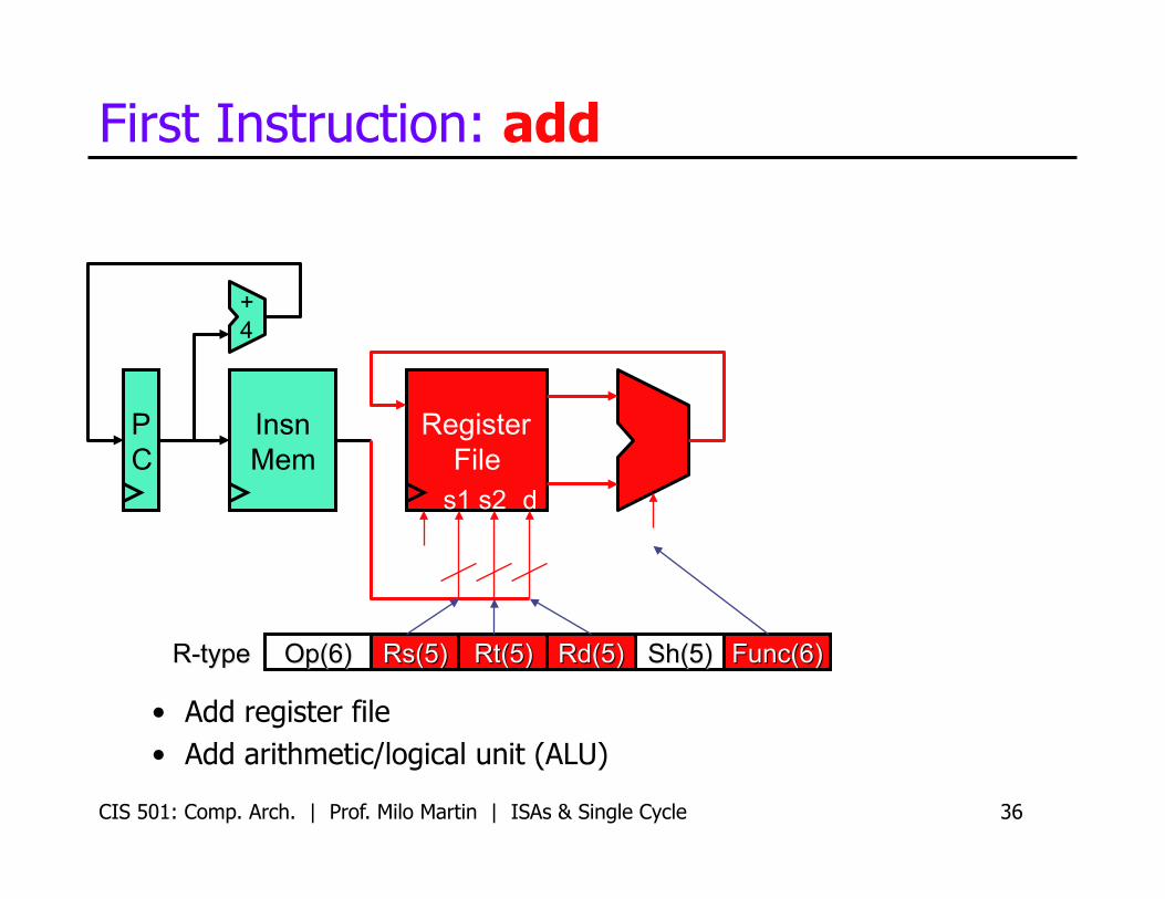
First Instruction: add
• Add register file • Add arithmetic/logical unit (ALU)
P C
Insn Mem
Register File
s1 s2 d
+ 4

Wire Select in Verilog
• How to rip out individual fields of an insn? Wire select wire [31:0] insn;!wire [5:0] op = insn[31:26];!wire [4:0] rs = insn[25:21];!wire [4:0] rt = insn[20:16];!wire [4:0] rd = insn[15:11];!wire [4:0] sh = insn[10:6];!wire [5:0] func = insn[5:0];!
CIS 501: Comp. Arch. | Prof. Milo Martin | ISAs & Single Cycle 37
CIS 501: Comp. Arch. | Prof. Milo Martin | ISAs & Single Cycle 38
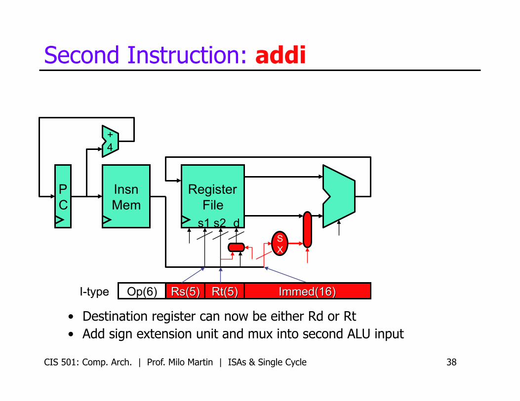
Second Instruction: addi
• Destination register can now be either Rd or Rt • Add sign extension unit and mux into second ALU input
P C
Insn Mem
Register File
S X
s1 s2 d
+ 4
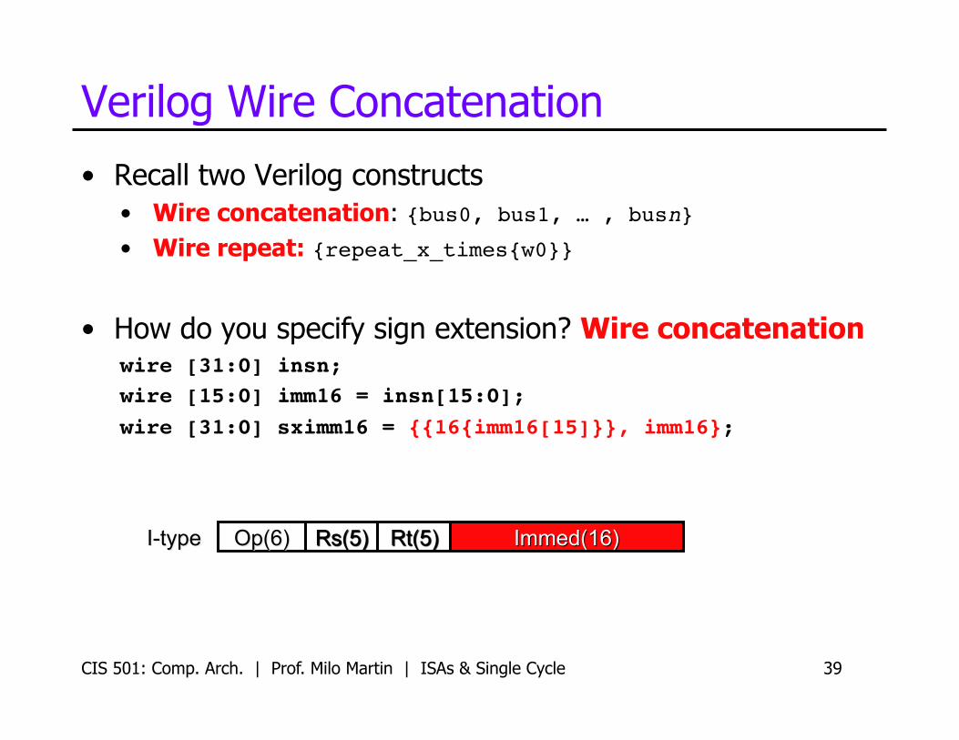
Verilog Wire Concatenation
• Recall two Verilog constructs • Wire concatenation: {bus0, bus1, … , busn}!• Wire repeat: {repeat_x_times{w0}}!
• How do you specify sign extension? Wire concatenation wire [31:0] insn;!wire [15:0] imm16 = insn[15:0];!wire [31:0] sximm16 = {{16{imm16[15]}}, imm16};!
CIS 501: Comp. Arch. | Prof. Milo Martin | ISAs & Single Cycle 39
CIS 501: Comp. Arch. | Prof. Milo Martin | ISAs & Single Cycle 40
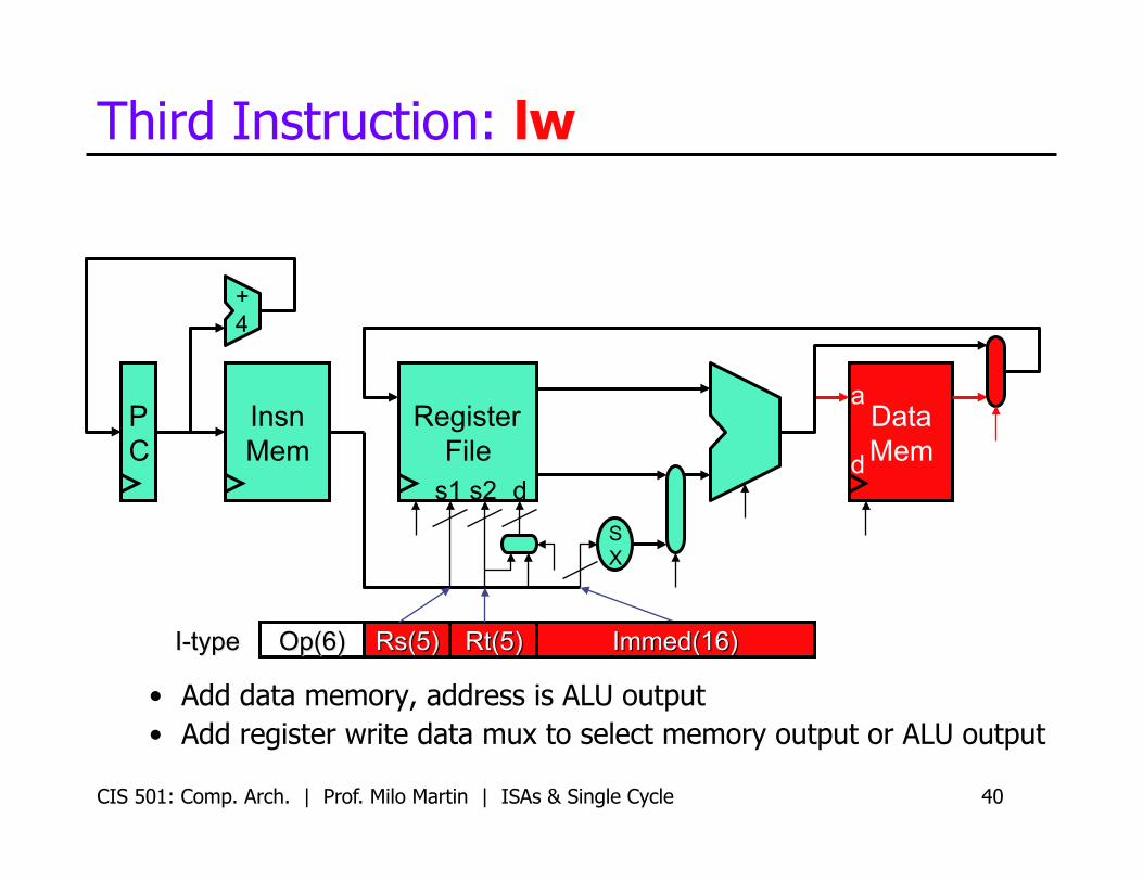
Third Instruction: lw
• Add data memory, address is ALU output • Add register write data mux to select memory output or ALU output
P C
Insn Mem
Register File
S X
s1 s2 d
Data Mem
a
d
+ 4
CIS 501: Comp. Arch. | Prof. Milo Martin | ISAs & Single Cycle 41
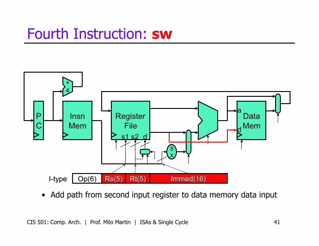
Fourth Instruction: sw
• Add path from second input register to data memory data input
P C
Insn Mem
Register File
S X
s1 s2 d
Data Mem
a
d
+ 4
CIS 501: Comp. Arch. | Prof. Milo Martin | ISAs & Single Cycle 42
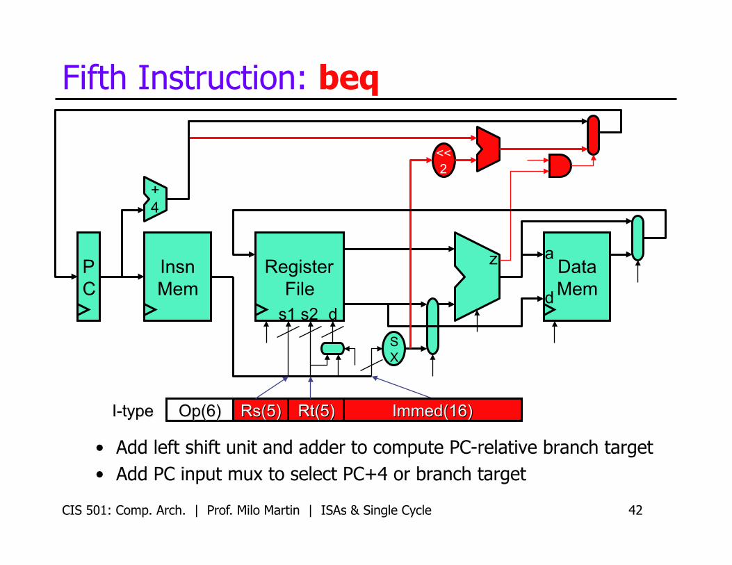
Fifth Instruction: beq
• Add left shift unit and adder to compute PC-relative branch target • Add PC input mux to select PC+4 or branch target
P C
Insn Mem
Register File
S X
s1 s2 d
Data Mem
a
d
+ 4
<< 2
z
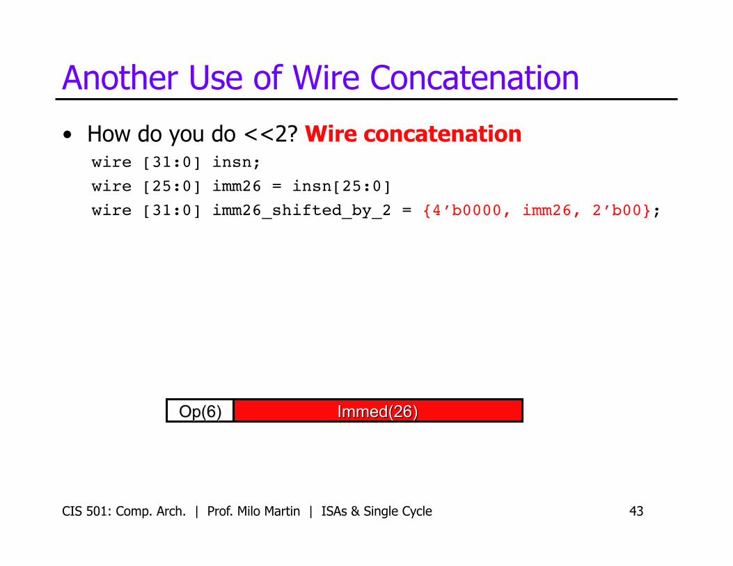
Another Use of Wire Concatenation
• How do you do <<2? Wire concatenation wire [31:0] insn;!wire [25:0] imm26 = insn[25:0]!wire [31:0] imm26_shifted_by_2 = {4’b0000, imm26, 2’b00};!
CIS 501: Comp. Arch. | Prof. Milo Martin | ISAs & Single Cycle 43
CIS 501: Comp. Arch. | Prof. Milo Martin | ISAs & Single Cycle 44
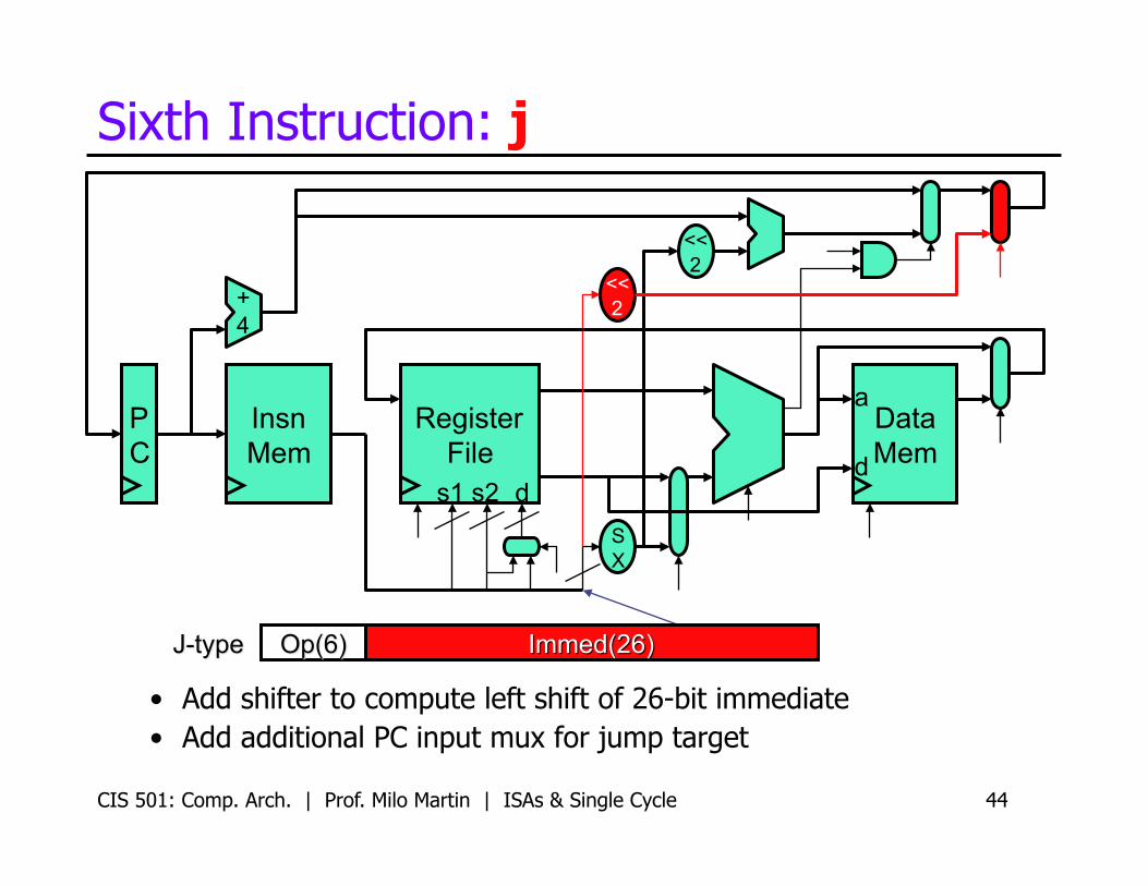
Sixth Instruction: j
• Add shifter to compute left shift of 26-bit immediate • Add additional PC input mux for jump target
P C
Insn Mem
Register File
S X
s1 s2 d
Data Mem
a
d
+ 4
<< 2
<< 2
MIPS Control
CIS 501: Comp. Arch. | Prof. Milo Martin | ISAs & Single Cycle 45

CIS 501: Comp. Arch. | Prof. Milo Martin | ISAs & Single Cycle 46
What Is Control?
• 9 signals control flow of data through this datapath • MUX selectors, or register/memory write enable signals • A real datapath has 300-500 control signals
P C
Insn Mem
Register File
S X
s1 s2 d
Data Mem
a
d
+ 4
<< 2
<< 2
Rwe
ALUinB
DMwe
JP
ALUop
BR
Rwd
Rdst
CIS 501: Comp. Arch. | Prof. Milo Martin | ISAs & Single Cycle 47
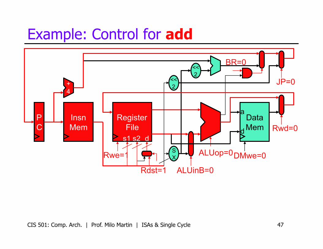
Example: Control for add
P C
Insn Mem
Register File
S X
s1 s2 d
Data Mem
a
d
+ 4
<< 2
<< 2
BR=0
JP=0
Rwd=0
DMwe=0 ALUop=0
ALUinB=0 Rdst=1
Rwe=1
CIS 501: Comp. Arch. | Prof. Milo Martin | ISAs & Single Cycle 48
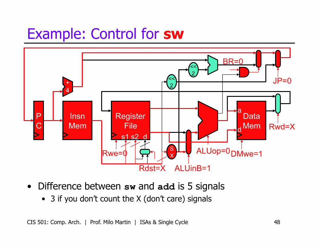
Example: Control for sw
• Difference between sw and add is 5 signals • 3 if you don’t count the X (don’t care) signals
P C
Insn Mem
Register File
S X
s1 s2 d
Data Mem
a
d
+ 4
<< 2
<< 2
Rwe=0
ALUinB=1
DMwe=1
JP=0
ALUop=0
BR=0
Rwd=X
Rdst=X
CIS 501: Comp. Arch. | Prof. Milo Martin | ISAs & Single Cycle 49
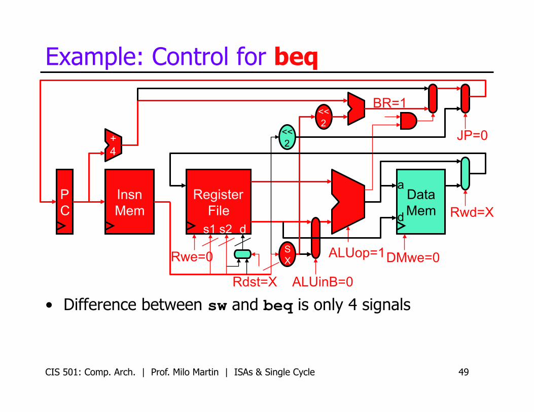
Example: Control for beq
• Difference between sw and beq is only 4 signals
P C
Insn Mem
Register File
S X
s1 s2 d
Data Mem
a
d
+ 4
<< 2
<< 2
Rwe=0
ALUinB=0
DMwe=0
JP=0
ALUop=1
BR=1
Rwd=X
Rdst=X
CIS 501: Comp. Arch. | Prof. Milo Martin | ISAs & Single Cycle 50
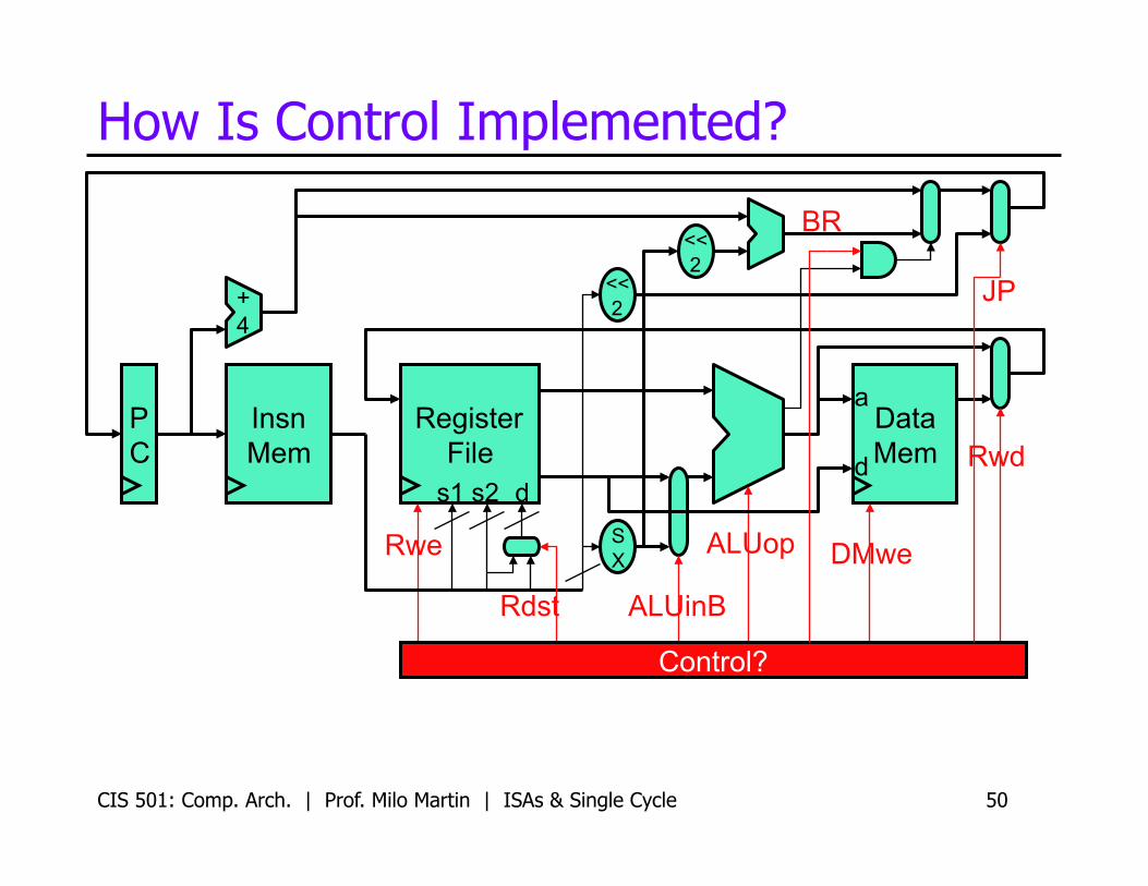
How Is Control Implemented?
P C
Insn Mem
Register File
S X
s1 s2 d
Data Mem
a
d
+ 4
<< 2
<< 2
Rwe
ALUinB
DMwe
JP
ALUop
BR
Rwd
Rdst
Control?

CIS 501: Comp. Arch. | Prof. Milo Martin | ISAs & Single Cycle 51
Implementing Control
• Each instruction has a unique set of control signals • Most are function of opcode • Some may be encoded in the instruction itself
• E.g., the ALUop signal is some portion of the MIPS Func field + Simplifies controller implementation • Requires careful ISA design
CIS 501: Comp. Arch. | Prof. Milo Martin | ISAs & Single Cycle 52
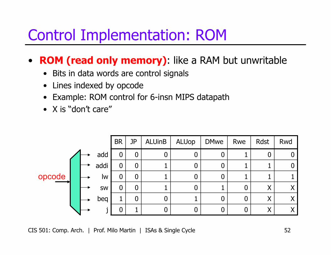
Control Implementation: ROM
• ROM (read only memory): like a RAM but unwritable • Bits in data words are control signals • Lines indexed by opcode • Example: ROM control for 6-insn MIPS datapath • X is “don’t care”
BR JP ALUinB ALUop DMwe Rwe Rdst Rwd
add 0 0 0 0 0 1 0 0
addi 0 0 1 0 0 1 1 0
lw 0 0 1 0 0 1 1 1
sw 0 0 1 0 1 0 X X
beq 1 0 0 1 0 0 X X
j 0 1 0 0 0 0 X X
opcode
CIS 501: Comp. Arch. | Prof. Milo Martin | ISAs & Single Cycle 53
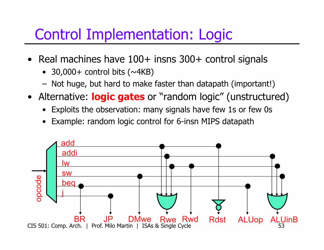
Control Implementation: Logic
• Real machines have 100+ insns 300+ control signals • 30,000+ control bits (~4KB) – Not huge, but hard to make faster than datapath (important!)
• Alternative: logic gates or “random logic” (unstructured) • Exploits the observation: many signals have few 1s or few 0s • Example: random logic control for 6-insn MIPS datapath
ALUinB
opco
de
add addi lw sw beq j
BR JP DMwe Rwd Rdst ALUop Rwe
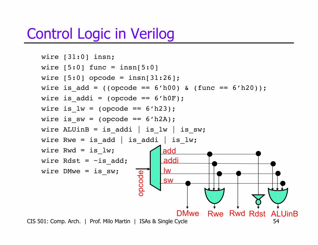
Control Logic in Verilog wire [31:0] insn;!wire [5:0] func = insn[5:0]!wire [5:0] opcode = insn[31:26];!wire is_add = ((opcode == 6’h00) & (func == 6’h20));!wire is_addi = (opcode == 6’h0F);!wire is_lw = (opcode == 6’h23);!wire is_sw = (opcode == 6’h2A);!wire ALUinB = is_addi | is_lw | is_sw; !wire Rwe = is_add | is_addi | is_lw;!wire Rwd = is_lw;!wire Rdst = ~is_add;!wire DMwe = is_sw;!
CIS 501: Comp. Arch. | Prof. Milo Martin | ISAs & Single Cycle 54 ALUinB
opco
de
add addi lw sw
DMwe Rwd Rdst Rwe
Datapath Storage Elements
CIS 501: Comp. Arch. | Prof. Milo Martin | ISAs & Single Cycle 55
CIS 501: Comp. Arch. | Prof. Milo Martin | ISAs & Single Cycle 56
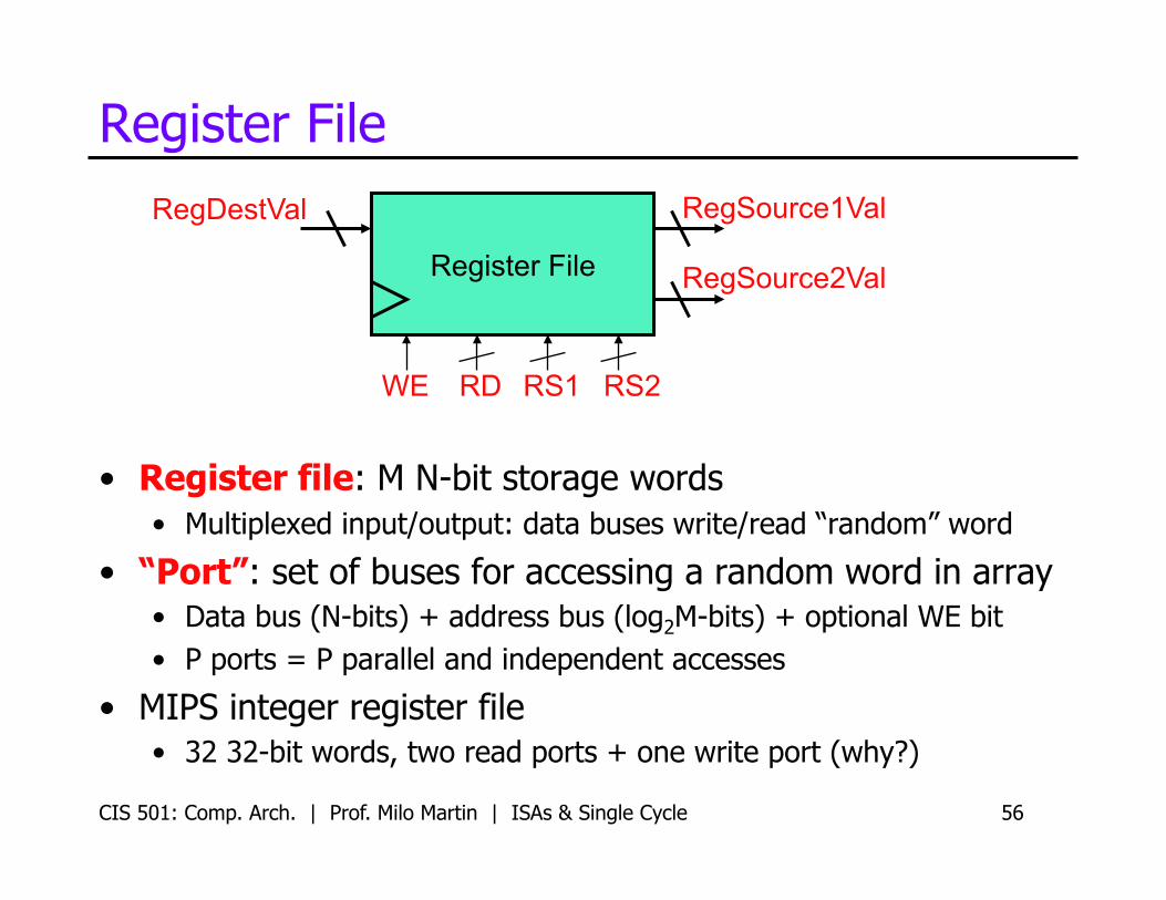
Register File
• Register file: M N-bit storage words • Multiplexed input/output: data buses write/read “random” word
• “Port”: set of buses for accessing a random word in array • Data bus (N-bits) + address bus (log2M-bits) + optional WE bit • P ports = P parallel and independent accesses
• MIPS integer register file • 32 32-bit words, two read ports + one write port (why?)
Register File
RegSource1Val
RegSource2Val
RegDestVal
RD WE RS1 RS2

CIS 501: Comp. Arch. | Prof. Milo Martin | ISAs & Single Cycle 57
Decoder
• Decoder: converts binary integer to “1-hot” representation • Binary representation of 0…2N–1: N bits • 1 hot representation of 0…2N–1: 2N bits
• J represented as Jth bit 1, all other bits zero • Example below: 2-to-4 decoder
B[0]
B[1] 1H[0]
1H[1]
1H[2]
1H[3]
B 1H
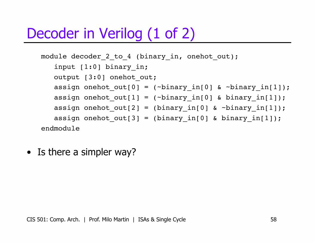
Decoder in Verilog (1 of 2) module decoder_2_to_4 (binary_in, onehot_out);! input [1:0] binary_in; ! output [3:0] onehot_out;! assign onehot_out[0] = (~binary_in[0] & ~binary_in[1]);! assign onehot_out[1] = (~binary_in[0] & binary_in[1]);! assign onehot_out[2] = (binary_in[0] & ~binary_in[1]);! assign onehot_out[3] = (binary_in[0] & binary_in[1]);!endmodule!
• Is there a simpler way?
CIS 501: Comp. Arch. | Prof. Milo Martin | ISAs & Single Cycle 58
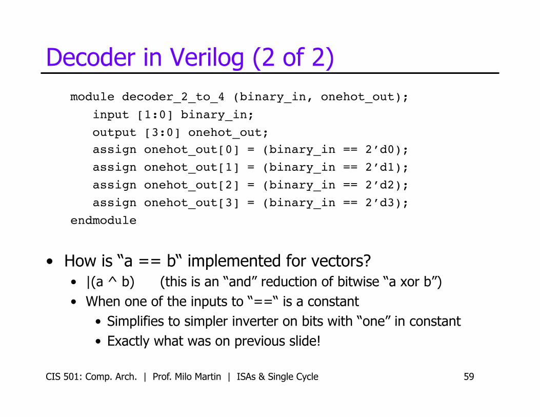
Decoder in Verilog (2 of 2) module decoder_2_to_4 (binary_in, onehot_out);! input [1:0] binary_in; ! output [3:0] onehot_out;! assign onehot_out[0] = (binary_in == 2’d0);! assign onehot_out[1] = (binary_in == 2’d1);! assign onehot_out[2] = (binary_in == 2’d2);! assign onehot_out[3] = (binary_in == 2’d3);!endmodule!
• How is “a == b“ implemented for vectors? • |(a ^ b) (this is an “and” reduction of bitwise “a xor b”) • When one of the inputs to “==“ is a constant
• Simplifies to simpler inverter on bits with “one” in constant • Exactly what was on previous slide!
CIS 501: Comp. Arch. | Prof. Milo Martin | ISAs & Single Cycle 59
CIS 501: Comp. Arch. | Prof. Milo Martin | ISAs & Single Cycle 60
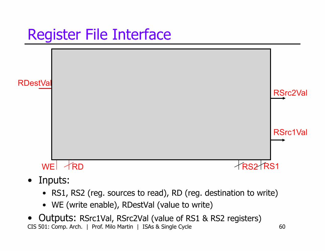
Register File Interface
• Inputs: • RS1, RS2 (reg. sources to read), RD (reg. destination to write) • WE (write enable), RDestVal (value to write)
• Outputs: RSrc1Val, RSrc2Val (value of RS1 & RS2 registers)
RS1
RSrc1Val
RSrc2Val
RS2 RD WE
RDestVal
CIS 501: Comp. Arch. | Prof. Milo Martin | ISAs & Single Cycle 61
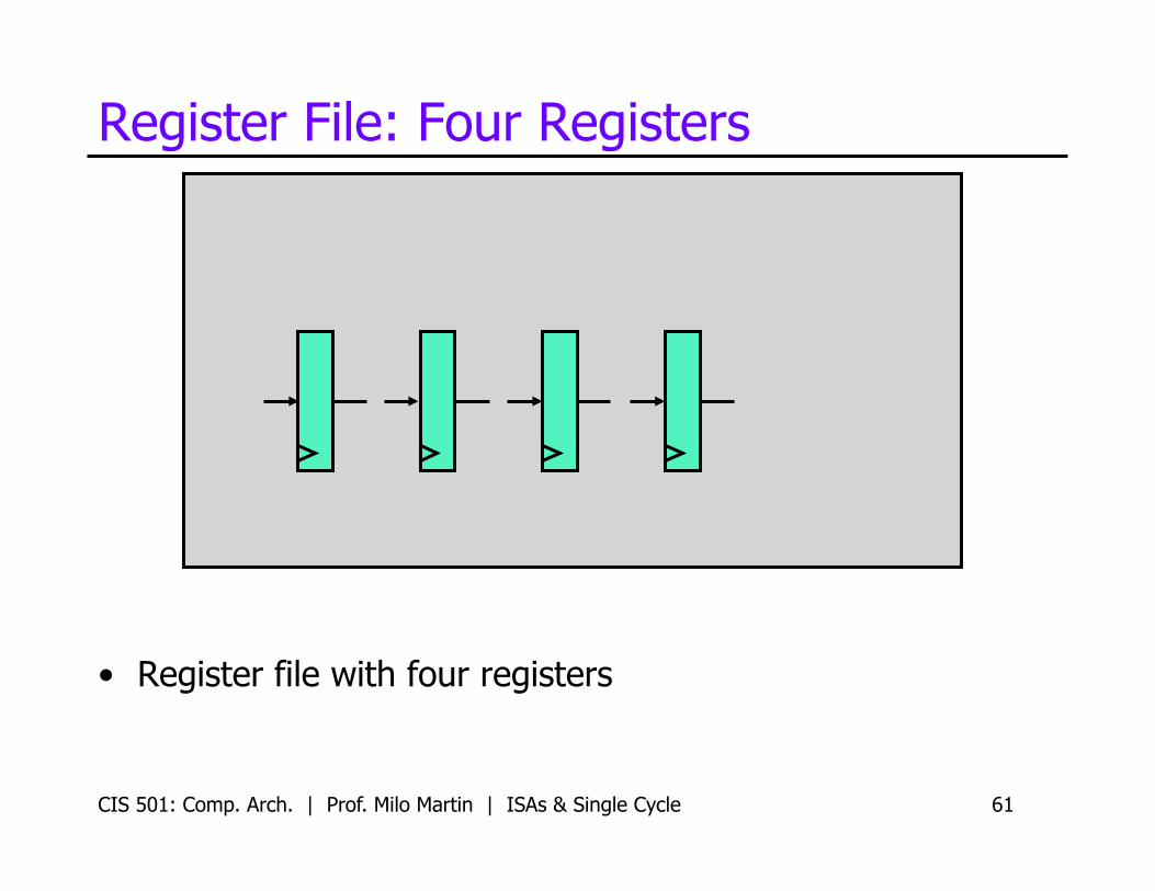
Register File: Four Registers
• Register file with four registers
CIS 501: Comp. Arch. | Prof. Milo Martin | ISAs & Single Cycle 62
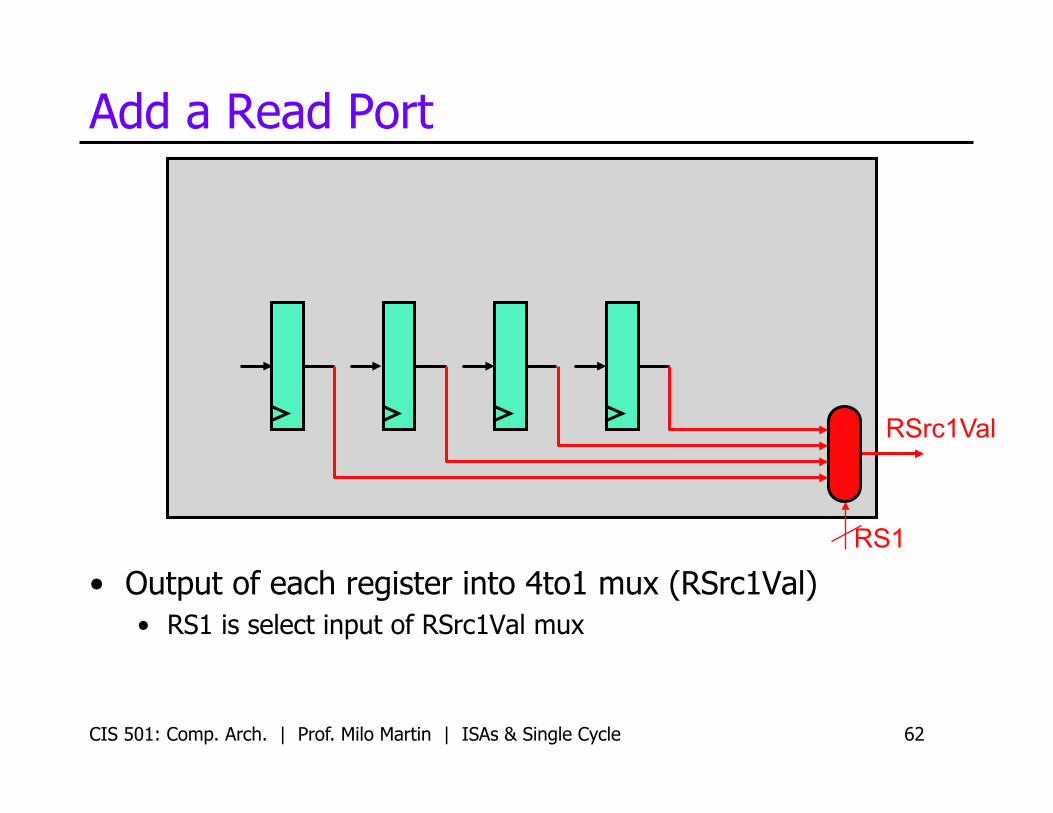
Add a Read Port
• Output of each register into 4to1 mux (RSrc1Val) • RS1 is select input of RSrc1Val mux
RS1
RSrc1Val
CIS 501: Comp. Arch. | Prof. Milo Martin | ISAs & Single Cycle 63
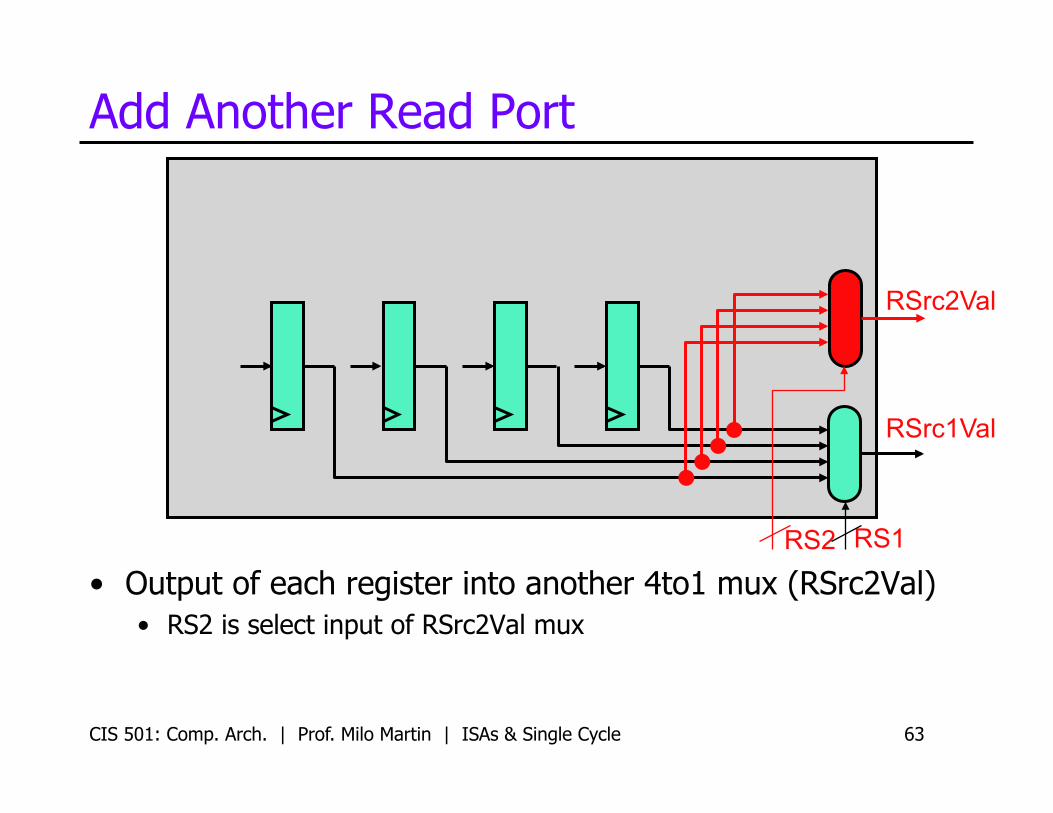
Add Another Read Port
• Output of each register into another 4to1 mux (RSrc2Val) • RS2 is select input of RSrc2Val mux
RS1
RSrc1Val
RSrc2Val
RS2

CIS 501: Comp. Arch. | Prof. Milo Martin | ISAs & Single Cycle 64
Add a Write Port
• Input RegDestVal into each register • Enable only one register’s WE: (Decoded RD) & (WE)
• What if we needed two write ports?
RS1
RSrc1Val
RSrc2Val
RS2 RD WE
RDestVal

Register File Interface (Verilog) module regfile4(rs1, rs1val, rs2, rs2val, rd, rdval, we, rst, clk);! parameter n = 1; ! input [1:0] rs1, rs2, rd; ! input we, rst, clk;! input [n-1:0] rdval; ! output [n-1:0] rs1val, rs2val;! …!
endmodule!
• Building block modules: • module register (out, in, wen, rst, clk);!• module decoder_2_to_4 (binary_in, onehot_out)!• module Nbit_mux4to1 (sel, a, b, c, d, out); !
CIS 501: Comp. Arch. | Prof. Milo Martin | ISAs & Single Cycle 65
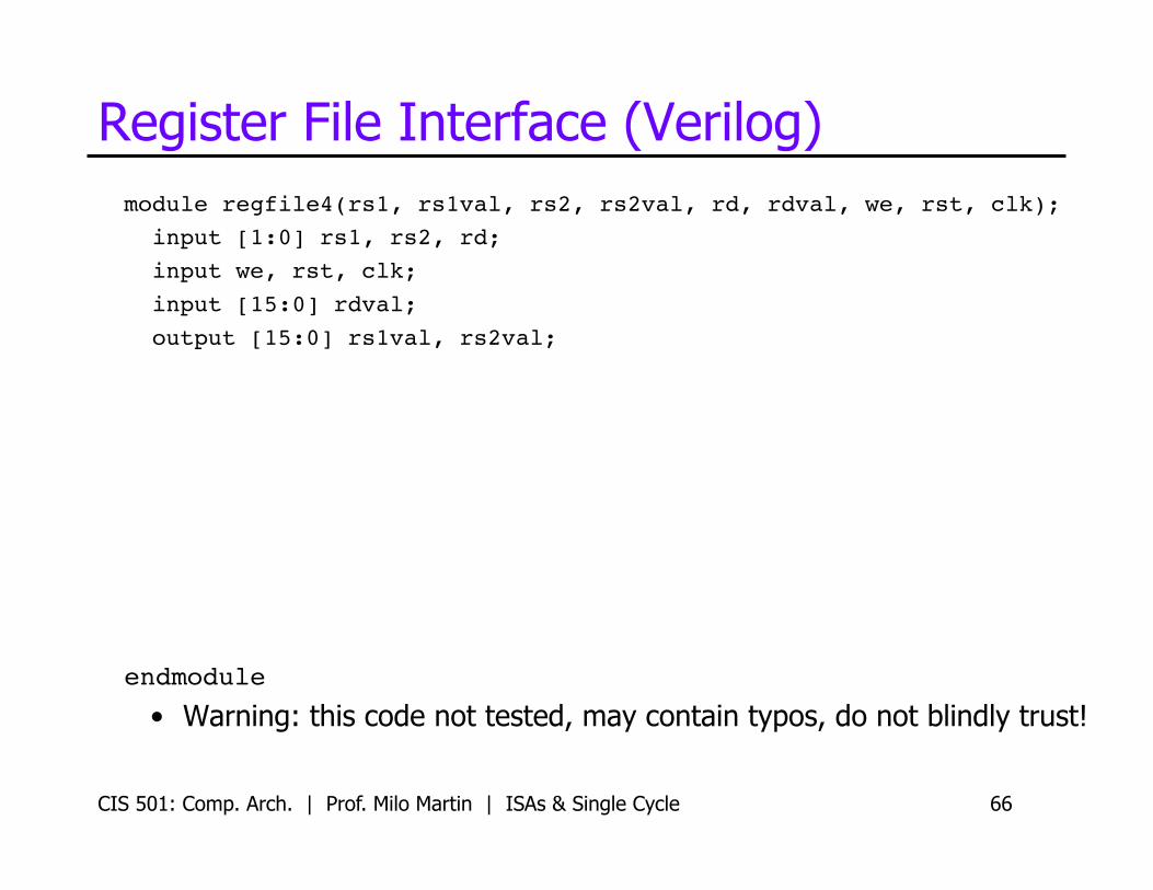
Register File Interface (Verilog) module regfile4(rs1, rs1val, rs2, rs2val, rd, rdval, we, rst, clk);! input [1:0] rs1, rs2, rd; ! input we, rst, clk;! input [15:0] rdval; ! output [15:0] rs1val, rs2val;!
endmodule!
• Warning: this code not tested, may contain typos, do not blindly trust!
CIS 501: Comp. Arch. | Prof. Milo Martin | ISAs & Single Cycle 66
[intentionally blank]
CIS 501: Comp. Arch. | Prof. Milo Martin | ISAs & Single Cycle 67
[intentionally blank]
CIS 501: Comp. Arch. | Prof. Milo Martin | ISAs & Single Cycle 68
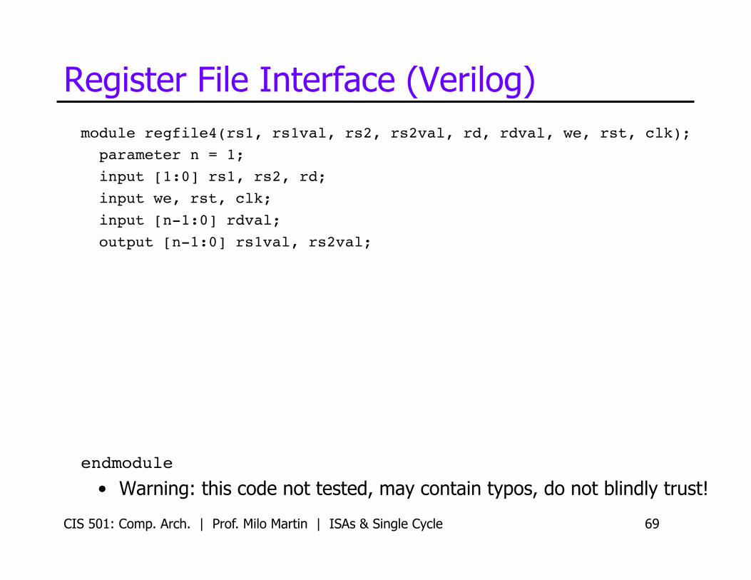
Register File Interface (Verilog) module regfile4(rs1, rs1val, rs2, rs2val, rd, rdval, we, rst, clk);! parameter n = 1; ! input [1:0] rs1, rs2, rd; ! input we, rst, clk;! input [n-1:0] rdval; ! output [n-1:0] rs1val, rs2val;!
endmodule!
• Warning: this code not tested, may contain typos, do not blindly trust!
CIS 501: Comp. Arch. | Prof. Milo Martin | ISAs & Single Cycle 69
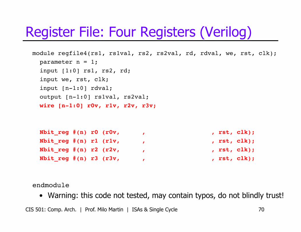
Register File: Four Registers (Verilog) module regfile4(rs1, rs1val, rs2, rs2val, rd, rdval, we, rst, clk);! parameter n = 1; ! input [1:0] rs1, rs2, rd; ! input we, rst, clk;! input [n-1:0] rdval; ! output [n-1:0] rs1val, rs2val;! wire [n-1:0] r0v, r1v, r2v, r3v;!
Nbit_reg #(n) r0 (r0v, , , rst, clk);! Nbit_reg #(n) r1 (r1v, , , rst, clk);! Nbit_reg #(n) r2 (r2v, , , rst, clk);! Nbit_reg #(n) r3 (r3v, , , rst, clk);!
endmodule!
• Warning: this code not tested, may contain typos, do not blindly trust!
CIS 501: Comp. Arch. | Prof. Milo Martin | ISAs & Single Cycle 70
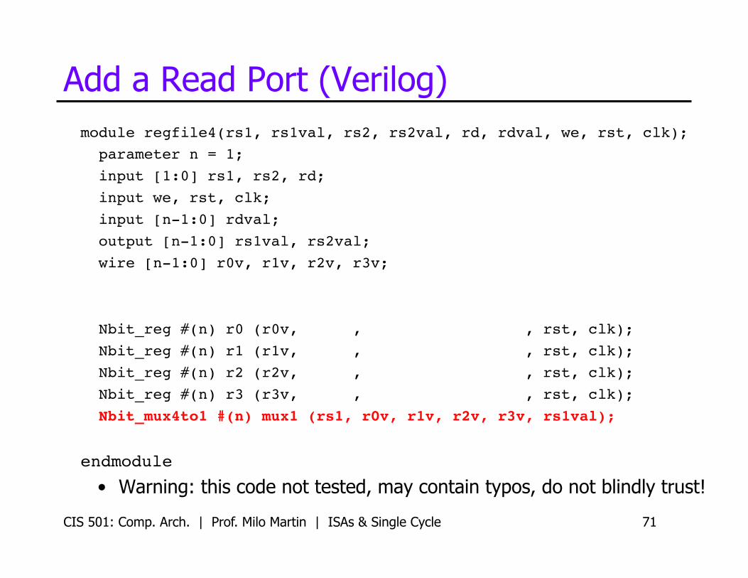
Add a Read Port (Verilog) module regfile4(rs1, rs1val, rs2, rs2val, rd, rdval, we, rst, clk);! parameter n = 1; ! input [1:0] rs1, rs2, rd; ! input we, rst, clk;! input [n-1:0] rdval; ! output [n-1:0] rs1val, rs2val;! wire [n-1:0] r0v, r1v, r2v, r3v;!
Nbit_reg #(n) r0 (r0v, , , rst, clk);! Nbit_reg #(n) r1 (r1v, , , rst, clk);! Nbit_reg #(n) r2 (r2v, , , rst, clk);! Nbit_reg #(n) r3 (r3v, , , rst, clk);! Nbit_mux4to1 #(n) mux1 (rs1, r0v, r1v, r2v, r3v, rs1val);!
endmodule!
• Warning: this code not tested, may contain typos, do not blindly trust!
CIS 501: Comp. Arch. | Prof. Milo Martin | ISAs & Single Cycle 71
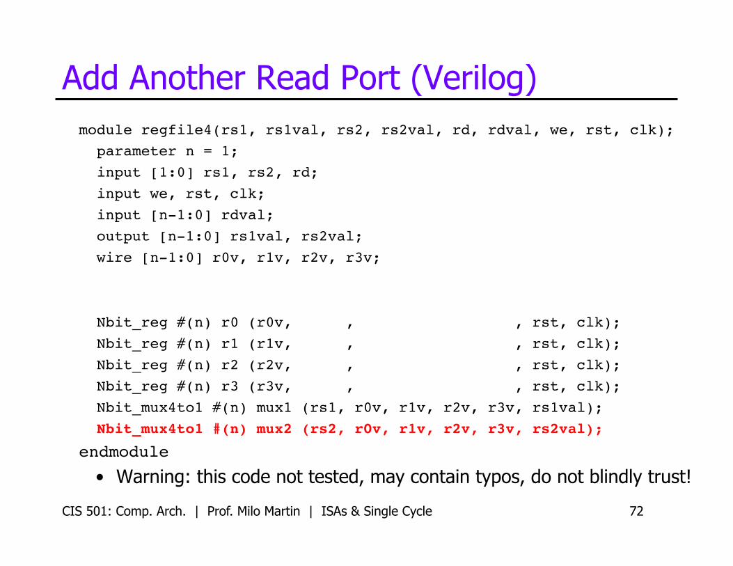
Add Another Read Port (Verilog) module regfile4(rs1, rs1val, rs2, rs2val, rd, rdval, we, rst, clk);! parameter n = 1; ! input [1:0] rs1, rs2, rd; ! input we, rst, clk;! input [n-1:0] rdval; ! output [n-1:0] rs1val, rs2val;! wire [n-1:0] r0v, r1v, r2v, r3v;!
Nbit_reg #(n) r0 (r0v, , , rst, clk);! Nbit_reg #(n) r1 (r1v, , , rst, clk);! Nbit_reg #(n) r2 (r2v, , , rst, clk);! Nbit_reg #(n) r3 (r3v, , , rst, clk);! Nbit_mux4to1 #(n) mux1 (rs1, r0v, r1v, r2v, r3v, rs1val);! Nbit_mux4to1 #(n) mux2 (rs2, r0v, r1v, r2v, r3v, rs2val);!
endmodule • Warning: this code not tested, may contain typos, do not blindly trust!
CIS 501: Comp. Arch. | Prof. Milo Martin | ISAs & Single Cycle 72
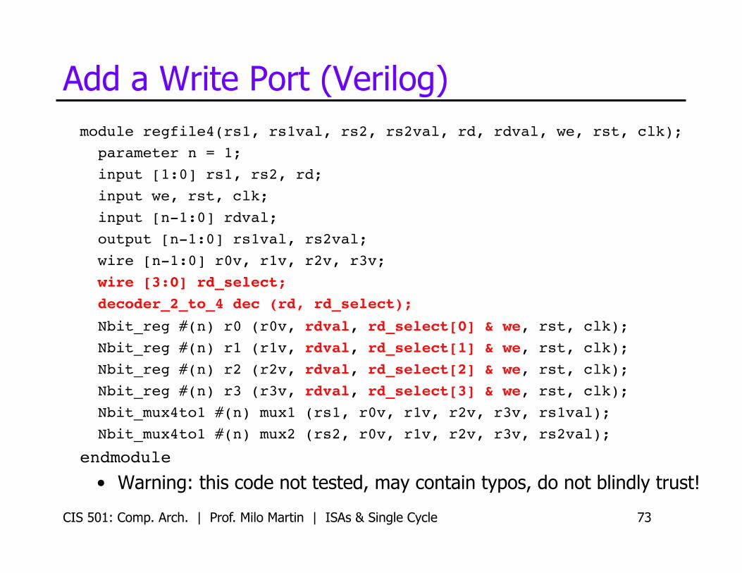
Add a Write Port (Verilog) module regfile4(rs1, rs1val, rs2, rs2val, rd, rdval, we, rst, clk);! parameter n = 1; ! input [1:0] rs1, rs2, rd; ! input we, rst, clk;! input [n-1:0] rdval; ! output [n-1:0] rs1val, rs2val;! wire [n-1:0] r0v, r1v, r2v, r3v;! wire [3:0] rd_select; ! decoder_2_to_4 dec (rd, rd_select);!
Nbit_reg #(n) r0 (r0v, rdval, rd_select[0] & we, rst, clk);! Nbit_reg #(n) r1 (r1v, rdval, rd_select[1] & we, rst, clk);! Nbit_reg #(n) r2 (r2v, rdval, rd_select[2] & we, rst, clk);! Nbit_reg #(n) r3 (r3v, rdval, rd_select[3] & we, rst, clk);! Nbit_mux4to1 #(n) mux1 (rs1, r0v, r1v, r2v, r3v, rs1val);! Nbit_mux4to1 #(n) mux2 (rs2, r0v, r1v, r2v, r3v, rs2val);!
endmodule!
• Warning: this code not tested, may contain typos, do not blindly trust!
CIS 501: Comp. Arch. | Prof. Milo Martin | ISAs & Single Cycle 73
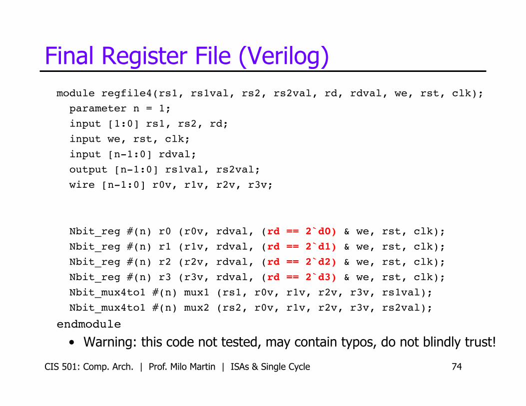
Final Register File (Verilog) module regfile4(rs1, rs1val, rs2, rs2val, rd, rdval, we, rst, clk);! parameter n = 1; ! input [1:0] rs1, rs2, rd; ! input we, rst, clk;! input [n-1:0] rdval; ! output [n-1:0] rs1val, rs2val;! wire [n-1:0] r0v, r1v, r2v, r3v;!
Nbit_reg #(n) r0 (r0v, rdval, (rd == 2`d0) & we, rst, clk);! Nbit_reg #(n) r1 (r1v, rdval, (rd == 2`d1) & we, rst, clk);! Nbit_reg #(n) r2 (r2v, rdval, (rd == 2`d2) & we, rst, clk);! Nbit_reg #(n) r3 (r3v, rdval, (rd == 2`d3) & we, rst, clk);! Nbit_mux4to1 #(n) mux1 (rs1, r0v, r1v, r2v, r3v, rs1val);! Nbit_mux4to1 #(n) mux2 (rs2, r0v, r1v, r2v, r3v, rs2val);!
endmodule!
• Warning: this code not tested, may contain typos, do not blindly trust!
CIS 501: Comp. Arch. | Prof. Milo Martin | ISAs & Single Cycle 74

CIS 501: Comp. Arch. | Prof. Milo Martin | ISAs & Single Cycle 75
Another Useful Component: Memory
• Register file: M N-bit storage words • Few words (< 256), many ports, dedicated read and write ports
• Memory: M N-bit storage words, yet not a register file • Many words (> 1024), few ports (1, 2), shared read/write ports
• Leads to different implementation choices • Lots of circuit tricks and such • Larger memories typically only 6 transistors per bit
• In Verilog? We’ll give you the code for large memories
Memory
DATAOUT DATAIN
WE
ADDRESS
Single-Cycle Performance
CIS 501: Comp. Arch. | Prof. Milo Martin | ISAs & Single Cycle 76
CIS 501: Comp. Arch. | Prof. Milo Martin | ISAs & Single Cycle 77
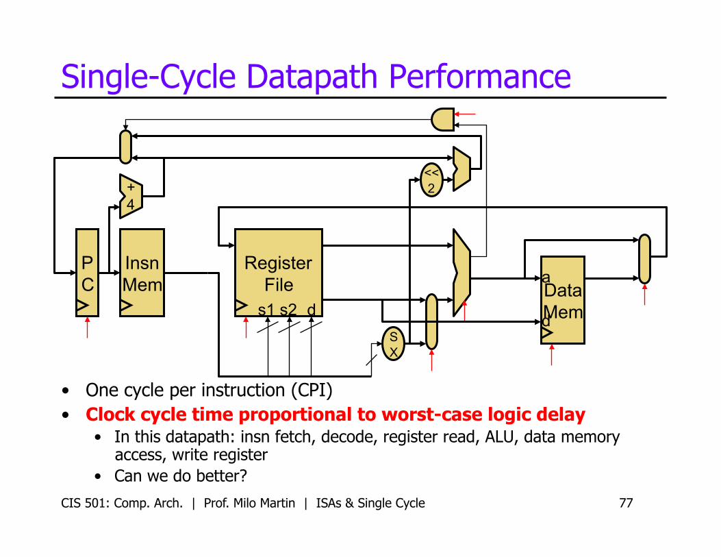
Single-Cycle Datapath Performance
• One cycle per instruction (CPI) • Clock cycle time proportional to worst-case logic delay
• In this datapath: insn fetch, decode, register read, ALU, data memory access, write register
• Can we do better?
P C
Insn Mem
Register File
S X
s1 s2 d Data Mem
a
d
+ 4
<< 2

CIS 501: Comp. Arch. | Prof. Milo Martin | ISAs & Single Cycle 78
Foreshadowing: Pipelined Datapath
• Split datapath into multiple stages • Assembly line analogy • 5 stages results in up to 5x clock & performance improvement
PC Insn Mem
Register File
S X
s1 s2 d Data Mem
a
d
+ 4
<< 2
PC
IR
PC
A
B
IR
O
B
IR
O
D
IR
CIS 501: Comp. Arch. | Prof. Milo Martin | ISAs & Single Cycle 79
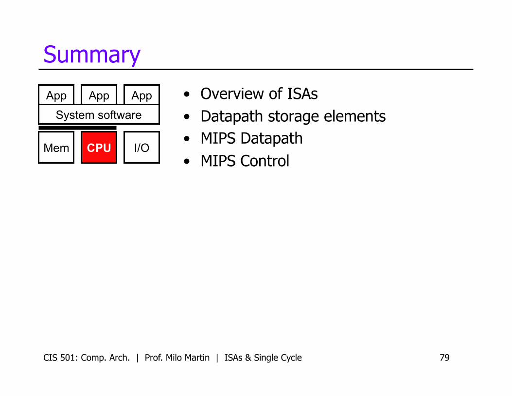
Summary
• Overview of ISAs • Datapath storage elements • MIPS Datapath • MIPS Control
CPU Mem I/O
System software
App App App