Embed Size (px)
Citation preview
CommuniCation
1801078 (1 of 11) © 2018 WILEY-VCH Verlag GmbH & Co. KGaA, Weinheim
www.advmat.de
Clarification of the Molecular Doping Mechanism in Organic Single-Crystalline Semiconductors and their Application in Color-Tunable Light-Emitting Devices
Ran Ding, Xue-Peng Wang, Jing Feng,* Xian-Bin Li,* Feng-Xi Dong, Wei-Quan Tian, Jia-Ren Du, Hong-Hua Fang, Hai-Yu Wang, Takeshi Yamao, Shu Hotta, and Hong-Bo Sun*
DOI: 10.1002/adma.201801078
as well as the energy-level alignment at interfaces between doped materials and metal contacts.[1,2] For instance, dopant atoms of Group III or Group V ele-ments are widely used to modulate the electrical conductivity of single-crystal silicon for the application of n-type or p-type devices in semiconductor-based integrated circuits.[16,17] Doping p-type gallium nitride with magnesium atoms gives rise to commercial products such as high-performance blue light-emitting devices (LEDs) and reliable violet laser diodes.[18,19] Dopant atoms within inor-ganic single-crystalline semiconductors are covalently bound to the surrounding matrix, introducing donor/acceptor states in the fundamental bandgap of the semiconductor.[1,2]
Among the organic semiconductors, amorphous and polycrystalline materials have been extensively investigated in the field of organic optoelectronics, because of their operational convenience.[20–22]
However, their intrinsic impurity and structural defects leads to low carrier mobility, which is one of the main limitations for the device performance.[23–34] Organic single-crystalline semiconductors constructed by π-conjugated molecules in long-range periodic order have emerged as unique optoelec-trical materials.[23–34] Their well-defined structures allow to gain
Organic single-crystalline semiconductors with long-range periodic order have attracted much attention for potential applications in electronic and optoelectronic devices due to their high carrier mobility, highly thermal stability, and low impurity content. Molecular doping has been proposed as a valuable strategy for improving the performance of organic semiconductors and semiconductor-based devices. However, a fundamental understanding of the inherent doping mechanism is still a key challenge impeding its practical application. In this study, solid evidence for the “perfect” substitutional doping mechanism of the stacking mode between the guest and host molecules in organic single-crystalline semiconductors using polarized photoluminescence spectrum measurements and first-principles calculations is provided. The molecular host–guest doping is further exploited for efficient color-tunable and even white organic single-crystal-based light-emitting devices by controlling the doping concentration. The clarification of the molecular doping mechanism in organic single-crystalline semiconductor host–guest system paves the way for their practical application in high-performance electronic and optoelectronic devices.
Molecular Doping
The ORCID identification number(s) for the author(s) of this article can be found under https://doi.org/10.1002/adma.201801078.
Dr. R. Ding, X.-P. Wang, Prof. J. Feng, Prof. X.-B. Li, F.-X. Dong, J.-R. Du Dr. H.-H. Fang, Prof. H.-Y. Wang, Prof. H.-B. SunState Key Laboratory of Integrated OptoelectronicsCollege of Electronic Science and EngineeringJilin University2699 Qianjin Street, Changchun 130012, ChinaE-mail: [email protected]; [email protected]. R. DingInternational Research Centre for Nano Handing and Manufacturing of China (CNM)Changchun University of Science and TechnologyChangchun 130022, China
Prof. W.-Q. TianCollege of Chemistry and Chemical EngineeringChongqing UniversityChongqing 400044, ChinaProf. T. Yamao, Prof. S. HottaDepartment of Macromolecular Science and EngineeringGraduate School of Science and TechnologyKyoto Institute of TechnologyMatsugasaki Sakyo-ku, Kyoto 606-8585, JapanProf. H.-B. SunState Key Lab of Precision Measurement Technology and InstrumentsDepartment of Precision InstrumentTsinghua UniversityHaidian, Beijing 100084, ChinaE-mail: [email protected]
In the study of modern semiconductor physics, doping tech-nology has a key role in determining the electrical and optical properties of semiconductor materials, and significantly affects the device performance.[1–15] Doping of inorganic semiconductors by controllably introducing impurity atoms is the basic method used to adjust the conductivity of materials
Adv. Mater. 2018, 30, 1801078
© 2018 WILEY-VCH Verlag GmbH & Co. KGaA, Weinheim1801078 (2 of 11)
www.advmat.dewww.advancedsciencenews.com
experimental access to the intrinsic fundamental electronic properties of organic semiconductors and semiconductor-based devices. Moreover, these materials with prominent fea-tures, such as high carrier mobility, highly thermal stability and low impurity content, have drawn significant attention for use in organic optoelectronic functional devices, such as opti-cally pumped lasers, organic field-effect transistors (OFETs), light-emitting organic field-effect transistors (LE-OFETs), and organic light-emitting devices (OLEDs).[32–45] Their molecular packing via intermolecular electronic coupling makes a great impact on the π-orbital overlap in crystal, therefore resulting in different electronic and optical properties of organic single-crystalline semiconductors.[23,32] The increase of the overlap between π-orbitals of adjacent molecules can cause delocalization of the polarons/excitons, leading to enhanced charge carrier mobility.[34] The highest mobility approaching ≈43 cm2 V−1 S−1 has been reported for the transistors based on rubrene single crystals, which is at least two orders of mag-nitude higher than amorphous organic semiconductors.[45] Furthermore, some emissive molecule-based organic single-crystalline semiconductors demonstrate advantages in optical properties.[23–27] For example, the fluorescent quantum effi-ciency of α,ω-di(biphenyl)-terthiophene (BP3T) single crystal has been estimated to exceed 80% with spectrally narrowed emissions.[44] Therefore, organic single-crystalline semiconduc-tors have been considered as promising candidates for high-performance optoelectronic devices.
Molecular doping also has been proposed as a valuable strategy to improve the performance of organic semiconduc-tors and their electronic and optoelectronic devices, targeting implementation in low-cost and large-scale electronic appli-cations.[2–15] According to the induced effects, the molecular doping can be distinguished into two different aspects of electrical doping and host–guest doping. In general, electrical doping by adding electron acceptor or electron donor mole-cules can dramatically increase the free charge carrier density of organic semiconductors.[2–10] On the other hand, the host–guest doping is an effective way to tune the emission proper-ties, where guest molecules are embedded into a host material matrix giving rise to charge trapping by guest molecules and energy transfer from the host to the guest.[11–15] By taking advantage of this host–guest system, molecular doping tech-nique is employed in organic single-crystalline semiconduc-tors to combine high mobility and the enhanced light-emitting properties. It allows to increase the photoluminescence (PL) internal quantum efficiency through suppressing luminescence quenching of the H-aggregate-like molecular dipole–dipole interaction.[46–63] Wang and co-workers have prepared the tet-racene- and pentacene-doped oligo(p-phenylenevinylene) crys-tals which exhibit high luminescent efficiency and color-tunable emission, and further elucidated their thermodynamics charac-teristics and charge transport properties.[46,47,50,51] Nakanotani and co-workers reported tetracene-doped oligo(p-phenylene-vinylene) crystals that displayed improved electroluminescence (EL) quantum efficiency under ambipolar operation in light-emitting OFETs.[54] They also found that thiophene/phenylene co-oligomer-doped oligo(p-phenylenevinylene) crystals possess tunable light-amplification characteristics with an extremely low-threshold amplified spontaneous emission.[55] Recently,
Parashchuk and co-workers even introduced a novel concept of self-doping by the synthesis of byproduct in thiophene/phe-nylene co-oligomer crystals which doubled the PL efficiency.[49] In addition, research on steady-state and time-resolved fluo-rescence measurements indicated that Förster energy transfer is the dominant process in the doped crystals.[48] The value of orientation factor in the doped crystals is most relevant to the energy transfer from host to guest molecules, which is advanta-geous for creating white light-emitting crystals by partial energy transfer.[56] Molecular host–guest doping is believed to be a promising strategy for creating organic single crystals with effi-cient EL and developing current-driven organic lasers.
However, the pace of understanding the doping mechanism of the basic stacking modes between host and guest molecules in organic single-crystalline semiconductors has lagged far behind the rapid progress in research on their applications.[49–56] It is generally believed that doping molecules are dispersed throughout the host crystal lattice by strong molecular interac-tions during crystal growth, and that their potential to replace the original host molecules in the crystal lattice is high. Moreover, the size of selected guest molecules is similar to that of the host molecules, and they are predicted to fill in defects or vacancies in the crystal lattice without distortion.[49–56] However, unam-biguous evidence of this doping mechanism of the stacking modes between host and guest molecules is lacking due to the difficulty in investigating organic small molecules at the nanoscale. It is therefore necessary to establish direct experi-mental access to recreate the origin of the doping mechanism in organic single-crystalline semiconductor host–guest system.
Here we use polarized PL spectra measurement and first-principles calculations of a doped organic single-crystal semi-conductor to provide a microscopic picture of the stacking modes between host and guest molecules in pentacene-doped 1,4-bis(4-methylstyryl)-benzene (BSB-Me) crystals. Energy transfer from host to guest molecules enables the color emis-sion to be tuned by adjusting the doping concentration. This molecular host–guest doping technology was then used to develop color-tunable and white single-crystal-based OLEDs, which exhibit a maximum luminance and current efficiency of 1100 cd m−2 and 0.91 cd A−1, respectively. Our discovery of a “perfect” substitutional doping mechanism could have impor-tant implications for the practical application of organic single-crystalline semiconductors in high-performance electronic and optoelectronic devices.
The host and guest materials, BSB-Me and pentacene (Figure 1a), were milled together as a mixed powder with doping concentrations of 1%, 3%, and 10% (1 and 100 mg, 3 and 100 mg, 10 and 100 mg, respectively). The pentacene-doped organic single crystals were grown from the mixed powder using the physical vapor transport method. Using the same sublimation and crystallization temperatures for penta-cene and BSB-Me ensured the successful growth of doped crys-tals.[48] By optimizing the crystal growth conditions, we obtained slice-shaped crystals with a thickness of less than 300 nm and a width of several millimeters (Figure 1b–e). Strong light emis-sion was observed from both the crystal edge and surface; the color emission ranged from pure blue to white, pink and red by changing the doping concentration from undoped to 1%, 3%, and 10%, respectively. The PL spectra of doped and undoped
Adv. Mater. 2018, 30, 1801078
© 2018 WILEY-VCH Verlag GmbH & Co. KGaA, Weinheim1801078 (3 of 11)
www.advmat.dewww.advancedsciencenews.com
crystals were measured under excitation using a 405 nm wave-length laser. The PL emission of pentacene in doped crystals peaked at 606 and 660 nm, whereas for the host BSB-Me, it peaked at 456, 486, and 521 nm (Figure 1f). For 1% doped crys-tals, the emissions from BSB-Me and pentacene were equally intense due to the partial energy transfer, which led to the emission of white light. And more suppression of the BSB-Me emission happens to 3% doped crystals compared to 1% doped ones. When the doping concentration increased to 10%, the emission from BSB-Me was almost completely suppressed due to the highly efficient energy transfer from host to guest molecules.
We investigated the time-resolved fluorescence of undoped and doped crystals to explore the energy transfer via a time-correlated single photon counting (TCSPC) system at the nano-second time scale. The TCSPC results and corresponding fitting curves of the undoped and 1%, 3%, 10% doped crystals were presented in Figure 1g which were monitored at the emission wavelength of 486 nm. After fitting analysis, the decay time τ0 of the undoped crystal was estimated to be 6.844 ns. At doping concentrations of 1%, 3%, and 10%, τ0 decreased to 4.457, 2.118, and 1.852 ns, respectively, indicating efficient energy transfer in the doped samples. The dominant energy transfer process has been proposed to be Förster energy transfer.[46–48] The rate of energy transfer from host to guest, kET, can be measured in the absence (τ0) and presence of an acceptor (τDA) by the equation: kET = 1/τDA − 1/τ0. The kET for doping con-centrations of 1%, 3%, and 10% were quantitatively calculated to be 7.82 × 10⁷, 3.26 × 10⁸, and 3.94 × 10⁸ s−1, respectively. Therefore, the energy transfer efficiency given by the equation
E = kET/(1/τ0 + kET) was calculated to be 34.8%, 69%, and 73% at the three concentrations, respectively. In addition, the decay time of pentacene in doped crystals monitored at 606 nm was prolonged from 8.48 to 9.055 ns, and then to 9.492 ns when the doping concentration was increased (Figure 1h). It is known that pentacene in crystalline form adopts a herringbone arrangement, which drastically quenches luminescence effi-ciency.[46–49,57–63] However, in this host–guest doping system, the efficient energy transfer effectively avoided the intermo-lecular aggregates and may contribute to a marked increase in luminescence efficiency.
The pentacene-doped crystals were characterized by their PL and TCSPC spectra. Here, a key question was raised: what are the basic stacking modes between the host and guest mole-cules, i.e., the sites of guest pentacene molecules, in the doped crystals? To investigate the doping mechanism, an optical meas-urement system was set up for the angle-resolved polarized PL experiments (Figure S1, Supporting Information).[64–66] The polarization measurements were performed using a polarizing microscope equipped with a mercury lamp as an excitation light source. The excitation light was focused perpendicularly incident to the crystal ab-plane, and the polarized PL emission was emitted parallel to the crystal plane and was guided to a detector through a contrast polarizer. Here the polarizer was used to analyze the polarization of the PL emission. The polar-ized PL was measured at the crystal edge in the direction ver-tical to the incident excitation light (Figure S1, Supporting Information). The polarized PL spectra were monitored at two major peaks: 486 nm for the host BSB-Me and 606 nm for the guest pentacene. Because the molecules are packed in a
Adv. Mater. 2018, 30, 1801078
Figure 1. Molecular structures and characterization of the doped crystals. a) Molecular structures of BSB-Me and pentacene. b–e) Top-view photographs under UV-light irradiation of undoped organic crystals (b), and crystals with a doping concentration of 1% (c), 3% (d), and 10% (e). Both the undoped and pentacene-doped BSB-Me crystals show a uniform surface emission. f) PL spectra of undoped and pentacene-doped BSB-Me crystals with different doping concentration. g,h) Nanosecond fluorescence decays from undoped and pentacene-doped BSB-Me crystals monitored at 486 nm (g) and 606 nm (h).
© 2018 WILEY-VCH Verlag GmbH & Co. KGaA, Weinheim1801078 (4 of 11)
www.advmat.dewww.advancedsciencenews.com
uniaxial orientation in the crystal, the peak intensity of PL spectra can be varied by rotating the polarizer. Observed from the intensity of polarized PL monitored at these two peaks, the angle-dependent polarization had the same trend along the a-axis of the crystal, whereas that polarization trend was reversed when the crystal is rotated 90° on the plane along the b-axis (Figure 2a,b). Figure 2c,d shows the relationship between PL intensity and the direction of polarization. The origin of angle-dependent polarization can be ascribed to the unique alignment of transition dipole moments.[67–69] We therefore calculated the molecular transition dipole moments of BSB-Me and pentacene using the Gaussian09 package (Figure S2, Sup-porting Information).[70] From the molecular-orbital calculation of BSB-Me and pentacene, the transition dipole moment was identified to be nearly parallel to the long axis of the BSB-Me molecule but perpendicular to the pentacene. The trend of angle-dependent polarization intensity implies that the transi-tion dipole moments of host and guest molecules are parallel along the a-axis of the crystal (Figure 2a,c). By contrast, the transition dipole moments of pentacene along the b-axis are perpendicular to those of BSB-Me (Figure 2b,d). In addition, the BSB-Me molecules are arranged in layers in a herringbone pattern and are inclined with respect to the crystal ab-plane. According to the crystal structure, the oblique angle of the tran-sition dipole moments with respect to the crystal ab-plane is almost 60°.[69] The angle-resolved polarized PL experiment revealed that the pentacene molecules inside the host BSB-Me crystal tend not only to stand alongside the BSB-Me molecules in the molecular long axis but also to have the greatest chance of replacing BSB-Me molecules in the crystal lattice. Figure 2e,f shows the alignment and spatial extent of the BSB-Me and
pentacene molecules and the molecular transition dipole moments in the crystal along the a-axis and b-axis, respectively. The blue and red vector arrows denote the molecular transition dipole moments of BSB-Me and pentacene molecules, respec-tively.[71] The vector projections of the BSB-Me and pentacene molecular transition dipole moments onto the bc-plane are perfectly parallel to each other (Figure 2e), whereas projections onto ac-plane are perpendicular to each other (Figure 2f).
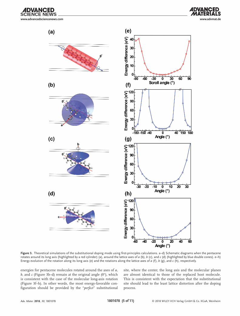
To further verify the substitutional doping mode of the pen-tacene guest molecules in the host BSB-Me crystal, we carried out theoretical simulations using first-principles calculation. The van der Waals interactions between the molecules play an important role in many physical and chemical systems. They are closely balanced with electrostatic and exchange-repulsion interactions and control the packing of molecules in crystal. Therefore, a density functional theory method (DFT-D2) containing a semi-empirical dispersion potential for the dis-persion force is used to describe the van der Waals interac-tions.[72–75] We focused on the substitutional site that was doped in the host crystal. We explored four typical rotational routes for pentacene in the BSB-Me crystal and traced their energy (Figure 3). The first route that we investigated is for the rotation around the long axis of the pentacene molecule, which is fixed to the original center of the replaced BSB-Me (Figure 3a). The lowest energy is at the original angle (0°), which indicates that the molecular plane of pentacene tends to be same as that of the replaced BSB-Me molecule (Figure 3e). In addition, Figure 3b–d displays the other three possible routes where the pentacene rotates around the axes of a, b, and c (passing through the pentacene molecular center) which are vertical to the bOc, aOc, and aOb plane, respectively. The lowest
Adv. Mater. 2018, 30, 1801078
Figure 2. The angle-resolved polarized PL measurements and molecular arrangement schematic of doped crystals. Relationship between the PL inten-sity and polarization angle which monitored at the emission peaks of BSB-Me (486 nm) and pentacene (606 nm). a–d) The polarizer rotates parallel to the bc-plane (a,c) and the ac-plane (b,d). e,f) Schematic drawings of the alignment of BSB-Me molecules and pentacene molecules along the a-axis and b-axis. The blue and red arrows represent the vector projections of transition dipole moments of BSB-Me and pentacene molecules, respectively: e) bc-plane view; f) ac-plane view.
© 2018 WILEY-VCH Verlag GmbH & Co. KGaA, Weinheim1801078 (5 of 11)
www.advmat.dewww.advancedsciencenews.com
energies for pentacene molecules rotated around the axes of a, b, and c (Figure 3b–d) remain at the original angle (0°), which is consistent with the case of the molecular long-axis rotation (Figure 3f–h). In other words, the most energy-favorable con-figuration should be provided by the “perfect” substitutional
site, where the center, the long axis and the molecular planes are almost identical to those of the replaced host molecule. This is consistent with the expectation that the substitutional site should lead to the least lattice distortion after the doping process.
Adv. Mater. 2018, 30, 1801078
Figure 3. Theoretical simulations of the substitutional doping mode using first-principles calculations. a–d) Schematic diagrams when the pentacene rotates around its long axis (highlighted by a red cylinder) (a), around the lattice axes of a (b), b (c), and c (d) (highlighted by blue double cones). e–h) Energy evolution of the rotation along its long axis (e) and the rotations along the lattice axes of a (f), b (g), and c (h), respectively.
© 2018 WILEY-VCH Verlag GmbH & Co. KGaA, Weinheim1801078 (6 of 11)
www.advmat.dewww.advancedsciencenews.com
In order to exploit the lattice distortion in the doped crys-tals, X-ray diffraction spectra of the undoped, 1%, 3%, and 10% doped crystals were characterized (Figure S4a, Supporting Information). The diffraction peak of the BSB-Me single crystal at 2θ of 13.57° (006) corresponded to the spacing of the c-axis. Using the Bragg equation, we calculated the thickness of one molecular layer to be 1.85 nm, indicating that the long axis of the molecules was perpendicular to the wide crystal and the ab-plane was parallel to the substrate.[54] There was no marked dif-ference in the diffraction peaks of the undoped BSB-Me and the pentacene-doped crystals, which appear at 2θ of 13.54°, 13.58°, and 13.60°. The coincident peak positions between the undoped and doped crystals implied that the molecular order of the BSB-Me host crystal lattice was retained even after 10% doping with pentacene. Meanwhile, no additional dif-fraction peaks appeared at all, suggesting that there were no pentacene-aggregated domain structures in the doped sam-ples. Figure S4b (Supporting Information) further showed the simulated X-ray diffraction spectra based on the present model which were compared to the experimental data. In the experi-ment, the doping process does not import any other impure phases (such as crystalline pentacene) and retains the char-acteristics of the host BSB-Me crystal. The theoretical X-ray diffraction in the substitutional model or the undoped BSB-Me model was well consistent with experimental data. Apart from the X-ray diffraction measurement, the possibility of the crystal deformation around the guest molecule was taken into account. The case of the pentacene molecule doped inside the BSB-Me crystal on the substitution site is further optimized inside the calculation cell. As shown in Figure S5 (Supporting Informa-tion), after the structure optimization, these is no significant deviation of the packing arrangement between the guest pen-tacene molecule and its surrounding BSB-Me molecules. In other words, the guest molecule on the substitution site leads to little deformation of surrounding host molecules. We also examined the possible interstitial site of pentacene doped in the host crystal matrix. Figure S6 (Supporting Information) shows a typical case. The interstitial site has a formation energy of 3.937 eV, which is significantly larger than that of the substi-tutional site, which is 0.0203 eV. Therefore, the interstitial site is hard to exist in the doped crystals. Based on these results, it is clear that the microscopic picture for the pentacene doped in BSB-Me crystals displays the substitutional mode.
A series of doped crystals are used in the fabrication of organic single-crystal-based OLEDs with a multilayered device structure comprising layers of gold (Au), molybdenum trioxide (MoO3), crystal, 2,2′2″-(1,3,5-benzinetriyl)-tris(1-phenyl-1-H-benzimidazole) (TPBi), calcium (Ca), and silver (Ag) based on the template stripping technique (Figure S7a, Supporting Infor-mation).[76–78] Both metal electrode films can be thermally evap-orated onto the opposite surface of the organic single crystals, ensuring a compact contact between the crystal and electrodes. The Au and Ca are chosen as anode and cathode with work functions of 5.1 and 2.87 eV,[79] respectively, by considering the highest-occupied molecular orbital (HOMO) and lowest-unoccupied molecular orbital (LUMO) levels of the BSB-Me crystal (5.6 and 2.7 eV, respectively).[80] Energy-level matching was used to promote charge injection and to balance holes and electrons in the recombination zone (Figure S7b, Supporting
Information).[78,81] The MoO3, a transition metal oxide inter-face layer with 5.3 eV, was subsequently deposited onto the Au anode as the anodic buffer layer, providing a work function gra-dient and ensuring hole injection.[82,83] TPBi, with a HOMO of 6.1 eV and a LUMO of 2.8 eV,[84–86] was employed as both an electron-transporting layer and a hole-blocking layer. Based on this configuration, the crystal-based OLEDs could achieve a sig-nificantly low turn-on voltage and high emission efficiency.
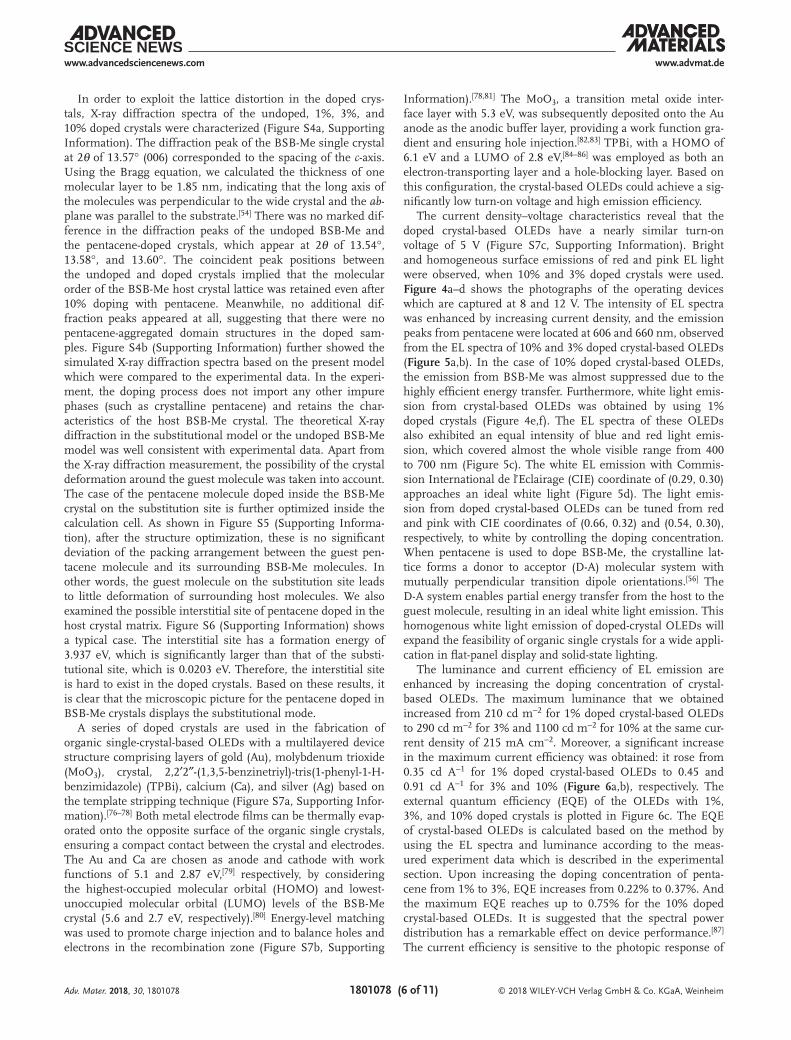
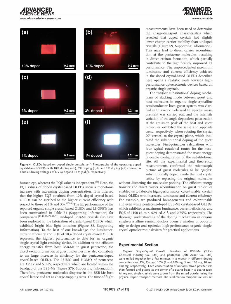
The current density–voltage characteristics reveal that the doped crystal-based OLEDs have a nearly similar turn-on voltage of 5 V (Figure S7c, Supporting Information). Bright and homogeneous surface emissions of red and pink EL light were observed, when 10% and 3% doped crystals were used. Figure 4a–d shows the photographs of the operating devices which are captured at 8 and 12 V. The intensity of EL spectra was enhanced by increasing current density, and the emission peaks from pentacene were located at 606 and 660 nm, observed from the EL spectra of 10% and 3% doped crystal-based OLEDs (Figure 5a,b). In the case of 10% doped crystal-based OLEDs, the emission from BSB-Me was almost suppressed due to the highly efficient energy transfer. Furthermore, white light emis-sion from crystal-based OLEDs was obtained by using 1% doped crystals (Figure 4e,f). The EL spectra of these OLEDs also exhibited an equal intensity of blue and red light emis-sion, which covered almost the whole visible range from 400 to 700 nm (Figure 5c). The white EL emission with Commis-sion International de l’Eclairage (CIE) coordinate of (0.29, 0.30) approaches an ideal white light (Figure 5d). The light emis-sion from doped crystal-based OLEDs can be tuned from red and pink with CIE coordinates of (0.66, 0.32) and (0.54, 0.30), respectively, to white by controlling the doping concentration. When pentacene is used to dope BSB-Me, the crystalline lat-tice forms a donor to acceptor (D-A) molecular system with mutually perpendicular transition dipole orientations.[56] The D-A system enables partial energy transfer from the host to the guest molecule, resulting in an ideal white light emission. This homogenous white light emission of doped-crystal OLEDs will expand the feasibility of organic single crystals for a wide appli-cation in flat-panel display and solid-state lighting.
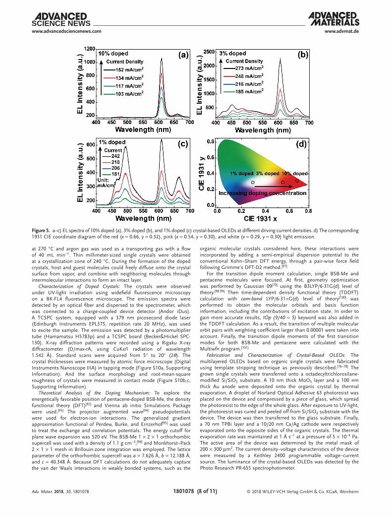
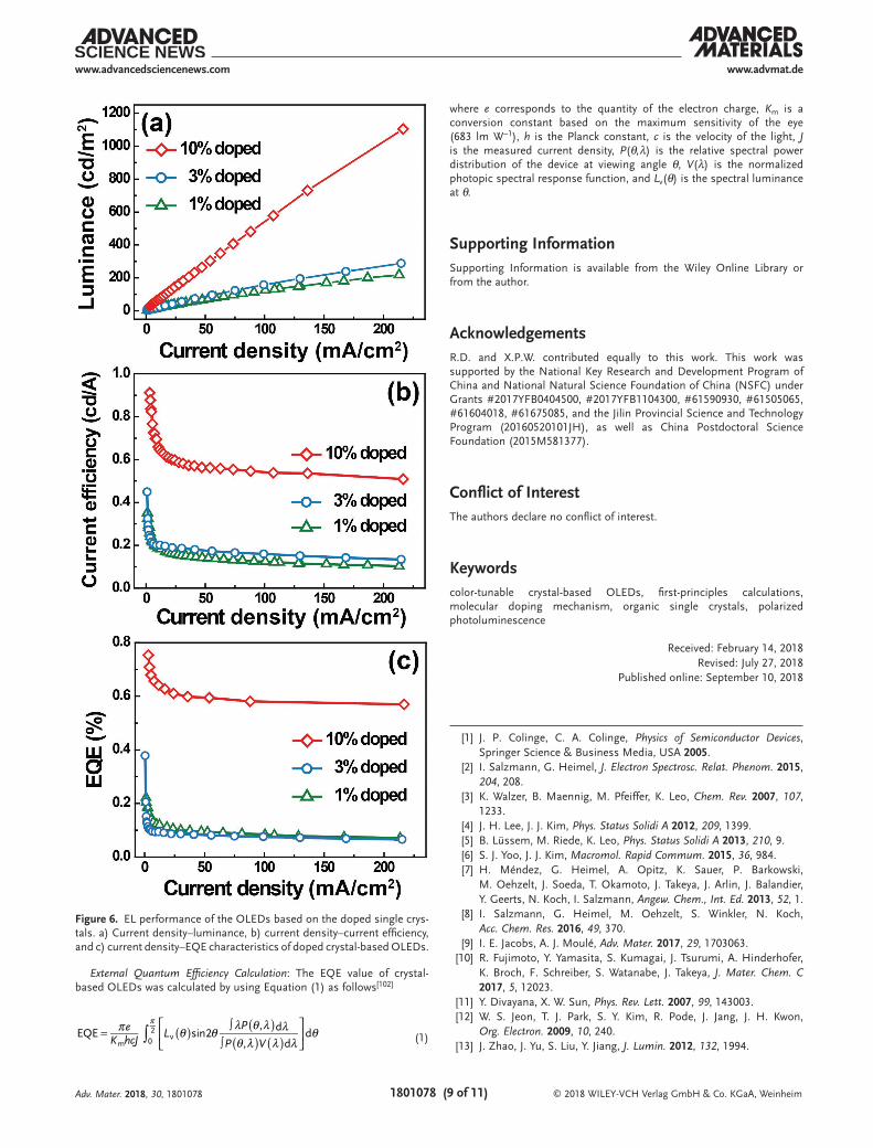
The luminance and current efficiency of EL emission are enhanced by increasing the doping concentration of crystal-based OLEDs. The maximum luminance that we obtained increased from 210 cd m−2 for 1% doped crystal-based OLEDs to 290 cd m−2 for 3% and 1100 cd m−2 for 10% at the same cur-rent density of 215 mA cm−2. Moreover, a significant increase in the maximum current efficiency was obtained: it rose from 0.35 cd A−1 for 1% doped crystal-based OLEDs to 0.45 and 0.91 cd A−1 for 3% and 10% (Figure 6a,b), respectively. The external quantum efficiency (EQE) of the OLEDs with 1%, 3%, and 10% doped crystals is plotted in Figure 6c. The EQE of crystal-based OLEDs is calculated based on the method by using the EL spectra and luminance according to the meas-ured experiment data which is described in the experimental section. Upon increasing the doping concentration of penta-cene from 1% to 3%, EQE increases from 0.22% to 0.37%. And the maximum EQE reaches up to 0.75% for the 10% doped crystal-based OLEDs. It is suggested that the spectral power distribution has a remarkable effect on device performance.[87] The current efficiency is sensitive to the photopic response of
Adv. Mater. 2018, 30, 1801078
© 2018 WILEY-VCH Verlag GmbH & Co. KGaA, Weinheim1801078 (7 of 11)
www.advmat.dewww.advancedsciencenews.com
human eye, whereas the EQE value is independent.[88] Here, the EQE values of doped crystal-based OLEDs show a monotonic increase with increasing doping concentration. It is inferred that the higher EQE obtained from 10% doped crystal-based OLEDs can be ascribed to the higher current efficiency with respect to those of 1% and 3%.[87,88] The EL performance of the reported organic single crystal-based OLEDs and LE-OFETs has been summarized in Table S1 (Supporting Information) for comparison.[33,42,76–78,89–91] Undoped BSB-Me crystals also have been exploited in the fabrication of crystal-based OLEDs which exhibited bright blue light emission (Figure S8, Supporting Information). To the best of our knowledge, the luminance, current efficiency and EQE of 10% doped crystal-based OLEDs represent the highest performance to date for an organic single-crystal light-emitting device. In addition to the efficient energy transfer from host BSB-Me to guest pentacene, the direct exciton formation at guest molecules may also contribute to the large increase in efficiency for the pentacene-doped crystal-based OLEDs. The LUMO and HOMO of pentacene are 3.2 eV and 5.0 eV, respectively, which are located within the bandgap of the BSB-Me (Figure S7b, Supporting Information). Therefore, pentacene molecules disperse in the BSB-Me host crystal lattice and act as charge-trapping sites. The time-of-flight
measurements have been used to determine the charge-transport characteristics which revealed that doped crystals had slightly lower charge carrier mobility than undoped crystals (Figure S9, Supporting Information). This may lead to direct carrier recombina-tion at the pentacene molecules, resulting in direct exciton formation, which partially contribute to the significantly improved EL performance. The unprecedented maximum luminance and current efficiency achieved in the doped crystal-based OLEDs described here opens a realistic route towards high-performance optoelectronic devices based on organic single crystals.
The “perfect” substitutional doping mecha-nism of stacking mode between guest and host molecules in organic single-crystalline semiconductor host–guest system was clari-fied in this work. Polarized PL spectra meas-urement was carried out, and the intensity variation of the angle-dependent polarization at the emission peak of the host and guest molecules exhibited the same and opposite trend, respectively, when rotating the crystal 90° vertical to the crystal plane, which indi-cated the substitutional doping of the guest molecules. First-principles calculations with four typical rotational routes for the host–guest doping demonstrated the most energy-favorable configuration of the substitutional site. All the experimental and theoretical measurements confirmed the microscopic picture of guest molecules to be “perfect” substitutionally doped inside the host crystal lattice by replacing the original molecules
without distorting the molecular packing. The efficient energy transfer and direct carrier recombination on guest molecules enabled us to fabricate high-performance, color-tunable, crystal-based OLEDs with increased luminance and current efficiency. For example, we produced homogeneous and color-tunable and even white pentacene-doped BSB-Me crystal-based OLEDs, which exhibited a maximum luminance, current efficiency, and EQE of 1100 cd m−2, 0.91 cd A−1, and 0.75%, respectively. The thorough understanding of the doping mechanism in organic single-crystalline semiconductors opens a window of opportu-nity to design and optimize high-performance organic single-crystal optoelectronic devices for practical applications.
Experimental SectionOrganic Single-Crystal Growth: Powders of BSB-Me (Tokyo
Chemical Industry Co., Ltd.) and pentacene (Alfa Aeser Co., Ltd.) were milled together for a few minutes in a mortar in different doping concentrations: 1%, 3%, and 10% (1 and 100 mg, 3 and 100 mg, 10 and 100 mg, respectively). Each concentration of uniform mixed powder was then formed and placed at the center of a quartz boat in a quartz tube. All organic single crystals were grown from the mixed powder using the physical vapor transport method. The sublimation temperature was set
Adv. Mater. 2018, 30, 1801078
Figure 4. OLEDs based on doped single crystals. a–f) Photographs of the operating doped crystal-based OLEDs with 10% doping (a,b), 3% doping (c,d), and 1% doping (e,f) concentra-tions at driving voltages of 8 V (a,c,e)and 12 V (b,d,f), respectively.
© 2018 WILEY-VCH Verlag GmbH & Co. KGaA, Weinheim1801078 (8 of 11)
www.advmat.dewww.advancedsciencenews.com
at 270 °C and argon gas was used as a transporting gas with a flow of 40 mL min−1. Thin millimeter-sized single crystals were obtained at a crystallization zone of 240 °C. During the formation of the doped crystals, host and guest molecules could freely diffuse onto the crystal surface from vapor, and combine with neighboring molecules through intermolecular interactions to form an intact layer.
Characterization of Doped Crystals: The crystals were observed under UV-light irradiation using widefield fluorescence microscopy on a BK-FL4 fluorescence microscope. The emission spectra were detected by an optical fiber and dispersed to the spectrometer, which was connected to a charge-coupled device detector (Andor iDus). A TCSPC system, equipped with a 379 nm picosecond diode laser (Edinburgh Instruments EPL375, repetition rate 20 MHz), was used to excite the sample. The emission was detected by a photomultiplier tube (Hamamatsu H5783p) and a TCSPC board (Becker&Hickel SPC-130). X-ray diffraction patterns were recorded using a Rigaku X-ray diffractometer (D/max-rA, using CuKα1 radiation of wavelength 1.542 Å). Standard scans were acquired from 5° to 20° (2θ). The crystal thicknesses were measured by atomic force microscope (Digital Instruments Nanoscope IIIA) in tapping mode (Figure S10a, Supporting Information). And the surface morphology and root-mean-square roughness of crystals were measured in contact mode (Figure S10b,c, Supporting Information).
Theoretical Analysis of the Doping Mechanism: To explore the energetically favorable position of pentacene-doped BSB-Me, the density functional theory (DFT)[92] and Vienna ab initio Simulations Package were used.[93] The projector augmented wave[94] pseudopotentials were used for electron-ion interactions. The generalized gradient approximation functional of Perdew, Burke, and Ernzerhof[95] was used to treat the exchange and correlation potentials. The energy cutoff for plane wave expansion was 520 eV. The BSB-Me 1 × 2 × 1 orthorhombic supercell was used with a density of 1.1 g cm−3,[96] and Monkhorst–Pack 2 × 1 × 1 mesh in Brillouin-zone integration was employed. The lattice parameter of the orthorhombic supercell was a = 7.626 Å, b = 12.188 Å, and c = 40.348 Å. Because DFT calculations do not adequately capture the van der Waals interactions in weakly bonded systems, such as the
organic molecular crystals considered here, these interactions were incorporated by adding a semi-empirical dispersion potential to the conventional Kohn–Sham DFT energy, through a pair-wise force field following Grimme’s DFT-D2 method.[97]
For the transition dipole moment calculation, single BSB-Me and pentacene molecules were focused. At first, geometry optimization was performed by Gaussian 09[70] using the B3LYP/6-31G(d) level of theory.[98,99] Then time-dependent density functional theory (TDDFT) calculation with cam-band LYP/6-31+G(d) level of theory[100] was performed to obtain the molecular orbitals and basis function information, including the contributions of excitation state. In order to gain more accurate results, IOp (9/40 = 5) keyword was also added in the TDDFT calculation. As a result, the transition of multiple molecular orbit pairs with weighting coefficient larger than 0.00001 were taken into account. Finally, the transition dipole moments of the first transition modes for both BSB-Me and pentacene were calculated with the Multiwfn program.[101]
Fabrication and Characterization of Crystal-Based OLEDs: The multilayered OLEDs based on organic single crystals were fabricated using template stripping technique as previously described.[76–78] The grown single crystals were transferred onto a octadecyltrichlorosilane-modified Si/SiO2 substrate. A 10 nm thick MoO3 layer and a 100 nm thick Au anode were deposited onto the organic crystal by thermal evaporation. A droplet of Norland Optical Adhesive 63 photoresist was placed on the device and compressed by a piece of glass, which spread the photoresist to the edge of the whole glass. After exposure to UV-light, the photoresist was cured and peeled off from Si/SiO2 substrate with the device. The device was then transferred to the glass substrate. Finally, a 70 nm TPBi layer and a 10/20 nm Ca/Ag cathode were respectively evaporated onto the opposite sides of the organic crystals. The thermal evaporation rate was maintained at 1 Å s−1 at a pressure of 5 × 10⁻⁴ Pa. The active area of the device was determined by the metal mask of 200 × 300 µm2. The current density–voltage characteristics of the device were measured by a Keithley 2400 programmable voltage–current source. The luminance of the crystal-based OLEDs was detected by the Photo Research PR-655 spectrophotometer.
Adv. Mater. 2018, 30, 1801078
Figure 5. a–c) EL spectra of 10% doped (a), 3% doped (b), and 1% doped (c) crystal-based OLEDs at different driving current densities. d) The corresponding 1931 CIE coordinate diagram of the red (x = 0.66, y = 0.32), pink (x = 0.54, y = 0.30), and white (x = 0.29, y = 0.30) light emission.
© 2018 WILEY-VCH Verlag GmbH & Co. KGaA, Weinheim1801078 (9 of 11)
www.advmat.dewww.advancedsciencenews.com
External Quantum Efficiency Calculation: The EQE value of crystal-based OLEDs was calculated by using Equation (1) as follows[102]
EQE sin2, d
, dd
mv0
2eK hcJ
LP
P V∫π θ θλ θ λ λθ λ λ λ
θ( )( ) ( )
( )=∫
∫
π
(1)
where e corresponds to the quantity of the electron charge, Km is a conversion constant based on the maximum sensitivity of the eye (683 lm W−1), h is the Planck constant, c is the velocity of the light, J is the measured current density, P(θ,λ) is the relative spectral power distribution of the device at viewing angle θ, V(λ) is the normalized photopic spectral response function, and Lv(θ) is the spectral luminance at θ.
Supporting InformationSupporting Information is available from the Wiley Online Library or from the author.
AcknowledgementsR.D. and X.P.W. contributed equally to this work. This work was supported by the National Key Research and Development Program of China and National Natural Science Foundation of China (NSFC) under Grants #2017YFB0404500, #2017YFB1104300, #61590930, #61505065, #61604018, #61675085, and the Jilin Provincial Science and Technology Program (20160520101JH), as well as China Postdoctoral Science Foundation (2015M581377).
Conflict of InterestThe authors declare no conflict of interest.
Keywordscolor-tunable crystal-based OLEDs, first-principles calculations, molecular doping mechanism, organic single crystals, polarized photoluminescence
Received: February 14, 2018Revised: July 27, 2018
Published online: September 10, 2018
[1] J. P. Colinge, C. A. Colinge, Physics of Semiconductor Devices, Springer Science & Business Media, USA 2005.
[2] I. Salzmann, G. Heimel, J. Electron Spectrosc. Relat. Phenom. 2015, 204, 208.
[3] K. Walzer, B. Maennig, M. Pfeiffer, K. Leo, Chem. Rev. 2007, 107, 1233.
[4] J. H. Lee, J. J. Kim, Phys. Status Solidi A 2012, 209, 1399.[5] B. Lüssem, M. Riede, K. Leo, Phys. Status Solidi A 2013, 210, 9.[6] S. J. Yoo, J. J. Kim, Macromol. Rapid Commum. 2015, 36, 984.[7] H. Méndez, G. Heimel, A. Opitz, K. Sauer, P. Barkowski,
M. Oehzelt, J. Soeda, T. Okamoto, J. Takeya, J. Arlin, J. Balandier, Y. Geerts, N. Koch, I. Salzmann, Angew. Chem., Int. Ed. 2013, 52, 1.
[8] I. Salzmann, G. Heimel, M. Oehzelt, S. Winkler, N. Koch, Acc. Chem. Res. 2016, 49, 370.
[9] I. E. Jacobs, A. J. Moulé, Adv. Mater. 2017, 29, 1703063.[10] R. Fujimoto, Y. Yamasita, S. Kumagai, J. Tsurumi, A. Hinderhofer,
K. Broch, F. Schreiber, S. Watanabe, J. Takeya, J. Mater. Chem. C 2017, 5, 12023.
[11] Y. Divayana, X. W. Sun, Phys. Rev. Lett. 2007, 99, 143003.[12] W. S. Jeon, T. J. Park, S. Y. Kim, R. Pode, J. Jang, J. H. Kwon,
Org. Electron. 2009, 10, 240.[13] J. Zhao, J. Yu, S. Liu, Y. Jiang, J. Lumin. 2012, 132, 1994.
Adv. Mater. 2018, 30, 1801078
Figure 6. EL performance of the OLEDs based on the doped single crys-tals. a) Current density–luminance, b) current density–current efficiency, and c) current density–EQE characteristics of doped crystal-based OLEDs.
© 2018 WILEY-VCH Verlag GmbH & Co. KGaA, Weinheim1801078 (10 of 11)
www.advmat.dewww.advancedsciencenews.com
[14] G. Li, D. Zhu, T. Peng, Y. Liu, Y. Wang, M. R. Bryce, Adv. Funct. Mater. 2014, 24, 7420.
[15] G. Zuo, Z. Li, O. Andersson, H. Abdalla, E. Wang, M. Kemerink, J. Phys. Chem. C 2017, 121, 7767.
[16] Neutron-Transmutation-Doped Silicon, (Ed.: J. Guldberg) Springer Science & Business Media, USA 2013.
[17] G. Eranna, Crystal Growth and Evaluation of Silicon for VLSI and ULSI, CRC Press, Boca Raton, FL, USA 2014.
[18] H. Amano, M. Kito, K. Hiramatsu, I. Akasaki, Jpn. J. Appl. Phys. 1989, 28, L2112.
[19] H. Amano, N. Sawaki, I. Akasaki, Y. Toyoda, Appl. Phys. Lett. 1986, 48, 353.
[20] I. D. W. Samuel, G. A. Turnbull, Chem. Rev. 2007, 107, 1272.[21] S. Gunes, H. Neugebauer, N. S. Sariciftci, Chem. Rev. 2007, 107,
1324.[22] A. J. Heeger, Chem. Soc. Rev. 2010, 39, 2354.[23] C. Wang, H. Dong, L. Jiang, W. Hu, Chem. Soc. Rev. 2018, 47, 422.[24] S. Hotta, T. Yamao, S. Z. Bisri, T. Takenobu, Y. Iwasa,
J. Mater. Chem. C 2014, 2, 965.[25] S. Hotta, T. Yamao, J. Mater. Chem. 2011, 21, 1295.[26] S. Hotta, Polym. Int. 2017, 66, 223.[27] S. Z. Bisri, T. Takenobu, Y. Iwasa, J. Mater. Chem. C 2014, 2, 2827.[28] J. Gierschner, S. Varghese, S. Y. Park, Adv. Opt. Mater. 2016, 4, 348.[29] A. J. C. Kuehne, M. C. Gather, Chem. Rev. 2016, 116, 12823.[30] H. H. Fang, J. Yang, J. Feng, T. Yamao, S. Hotta, H.-B. Sun, Laser
Photonics Rev. 2014, 8, 687.[31] S. Z. Bisri, C. Piliego, J. Gao, M. A. Loi, Adv. Mater. 2014, 26, 1176.[32] H. Dong, X. Fu, J. Liu, Z. Wang, W. Hu, Adv. Mater. 2013, 25, 6158.[33] H. Wang, Z. Xie, Y. Ma, J. Shen, Sci. China: Chem. 2007, 50, 433.[34] C. Y. Liu, A. J. Bard, Acc. Chem. Res. 1999, 32, 235.[35] T. Takahashi, T. Takenobu, J. Takeya, Y. Iwasa, Adv. Funct. Mater.
2007, 17, 1623.[36] T. Yamao, Y. Sakurai, K. Terasaki, Y. Shimizu, H. Jinnai, S. Hotta,
Adv. Mater. 2010, 22, 3708.[37] K. Sawabe, M. Imakawa, M. Nakano, T. Yamao, S. Hotta, Y. Iwasa,
T. Takenobu, Adv. Mater. 2012, 24, 6141.[38] S. Z. Bisri, K. Sawabe, M. Imakawa, K. Maruyama, T. Yamao,
S. Hotta, Y. Iwasa, T. Takenobu, Sci. Rep. 2012, 2, 985.[39] S. Z. Bisri, T. Takenobu, K. Sawabe, S. Tsuda, Y. Yomogida,
T. Yamao, S. Hotta, C. Adachi, Y. Iwasa, Adv. Mater. 2011, 23, 2753.
[40] L. Jiang, W. Hu, Z. Wei, W. Xu, H. Meng, Adv. Mater. 2009, 21, 3649.
[41] H. Jiang, H. Zhao, K. K. Zhang, X. Chen, C. Kloc, W. Hu, Adv. Mater. 2011, 23, 5075.
[42] H. Nakanotani, C. Adachi, Appl. Phys. Lett. 2010, 96, 053301.[43] H. Wang, F. Li, I. Ravia, B. Gao, Y. Li, V. Medvedev, H. B. Sun,
N. Tessler, Y. Ma, Adv. Funct. Mater. 2011, 21, 3770.[44] S. Z. Bisri, T. Takenobu, Y. Yomogida, H. Shimotani, T. Yamao,
S. Hotta, Y. Iwasa, Adv. Funct. Mater. 2009, 19, 1728.[45] M. Yamagishi, J. Takeya, Y. Tominari, Y. Nakazawa, T. Kuroda,
S. Ikehata, M. Uno, T. Nishikawa, T. Kawase, Appl. Phys. Lett. 2007, 90, 182117.
[46] H. Wang, Y. Zhao, Z. Xie, H. Wang, B. Wang, Y. Ma, CrystEngComm 2014, 16, 4539.
[47] H. Wang, F. Li, B. Gao, Z. Xie, S. Liu, C. Wang, D. Hu, F. Shen, Y. Xu, H. Shang, Q. Chen, Y. Ma, H. B. Sun, Cryst. Growth Des. 2009, 9, 4945.
[48] H. H. Fang, S. Y. Lu, L. Wang, R. Ding, H. Y. Wang, J. Feng, Q. D. Chen, H. B. Sun, Org. Electron. 2013, 14, 389.
[49] O. D. Parashchuk, A. A. Mannanov, V. G. Konstantinov, D. I. Dominskiy, N. M. Surin, O. V. Borshchev, S. A. Ponomarenko, M. S. Pshenichnikov, D. Y. Paraschuk, Adv. Funct. Mater. 2018, 28, 1800116.
[50] H. Wang, Y. Zhao, Z. Xie, H. Shang, H. Wang, F. Li, Y. Ma, CrystEngComm 2015, 17, 2168.
[51] Y. Zhao, X. Wang, M. Li, B. Zhang, H. Wang, Synth. Met. 2017, 223, 12.
[52] J. H. Wu, Z. Guan, T. Z. Xu, Q. H. Xu, G. Q. Xu, Langmuir 2011, 27, 6374.
[53] J. Li, S. Tkaishi, N. Fujinuma, K. Endo, M. Yamashita, H. Matsuzaki, H. Okamoto, K. Sawabe, T. Takenobu, Y. Iwasa, J. Mater. Chem. 2011, 21, 17662.
[54] H. Nakanotani, M. Saito, H. Nakamura, C. Adachi, Adv. Funct. Mater. 2010, 20, 1610.
[55] H. Nakanotani, C. Adachi, Adv. Opt. Mater. 2013, 1, 422.[56] H. Wang, B. Yue, Z. Xie, B. Gao, Y. Xu, L. Liu, H. B. Sun, Y. Ma,
Phys. Chem. Chem. Phys. 2013, 15, 3527.[57] F. C. Spano, C. Silva, Annu. Rev. Phys. Chem. 2014, 65, 477.[58] R. M. Hochstrasser, M. Kasha, Photochem. Photobiol. 1964, 3, 317.[59] M. Kasha, Radiat. Res. 1963, 20, 55.[60] E. G. McRae, M. Kasha, J. Chem. Phys. 1958, 28, 721.[61] F. C. Spano, J. Phys. Chem. 2003, 118, 981.[62] F. C. Spano, Acc. Chem. Res. 2009, 43, 429.[63] F. C. Spano, Annu. Rev. Phys. Chem. 2006, 57, 217.[64] T. Yamao, Y. Taniguchi, K. Yamamoto, T. Miki, T. Ohira, S. Hotta,
Jpn. J. Appl. Phys. 2008, 47, 4719.[65] T. Yamao, T. Ohira, S. Ota, S. Hotta, J. Appl. Phys. 2007, 101,
083517.[66] K. Zhanghao, L. Chen, X. Yang, M. Y. Wang, Z. L. Jing, H. B. Han,
M. Zhang, D. Y. Jin, J. Gao, P. Xi, Light: Sci. Appl. 2016, 5, e16166.
[67] S. Hotta, M. Goto, R. Azumi, M. Inoue, M. Ichikawa, Y. Taniguchi, Chem. Mater. 2004, 16, 237.
[68] Y. Yomogida, H. Sakai, K. Sawabe, S. Gocho, S. Z. Bisri, H. Nakanotani, C. Adachi, T. Hasobe, Y. Iwasa, T. Takenobu, Org. Electron. 2013, 14, 2737.
[69] R. Kabe, H. Nakanotani, T. Sakanoue, M. Yahiro, C. Adachi, Adv. Mater. 2009, 21, 4034.
[70] Gaussian 09, Gaussian, Inc, Wallingford, CT, USA 2009.[71] K. Bando, T. Nakamura, S. Fujiwara, Y. Masumoto, F. Sasaki,
S. Kobayashi, Y. Shimoi, S. Hotta, Phys. Rev. B 2008, 77, 045205.[72] V. G. Ruiz, W. Liu, E. Zojer, M. Scheffler, A. Tkatchenko,
Phys. Rev. Lett. 2012, 108, 146103.[73] M. A. Neumann, M. A. Perrin, J. Phys. Chem. B 2005, 109, 15531.[74] T. Bucko, J. Hafner, S. Lebegue, J. G. Angyán, J. Phys. Chem. A
2010, 114, 11814.[75] S. V. Aradhya, M. Frei, M. S. Hybertsen, L. Venkataraman,
Nat. Mater. 2012, 11, 872.[76] R. Ding, J. Feng, X. L. Zhang, W. Zhou, H. H. Fang, Y. F. Liu,
Q. D. Chen, H. Y. Wang, H. B. Sun, Adv. Funct. Mater. 2014, 24, 7085.
[77] R. Ding, J. Feng, W. Zhou, X. L. Zhang, H. H. Fang, T. Yang, H. Y. Wang, S. Hotta, H. B. Sun, Sci. Rep. 2015, 5, 12445.
[78] R. Ding, J. Feng, F. X. Dong, W. Zhou, Y. Liu, X. L. Zhang, X. P. Wang, H. H. Fang, B. Xu, X. B. Li, H. Y. Wang, S. Hotta, H. B. Sun, Adv. Funct. Mater. 2017, 27, 1604659.
[79] http://www.kayelaby.npl.co.uk/.[80] H. Nakanotani, R. Kabe, M. Yahiro, T. Takenobu, Y. Iwasa,
C. Adachi, Appl. Phys. Express 2008, 1, 091801.[81] Y. H. Chen, D. G. Ma, H. D. Sun, J. S. Chen, Q. X. Guo, Q. Wang,
Y. B. Zhao, Light: Sci. Appl. 2016, 5, e16042.[82] F. J. Zhang, D. W. Zhao, Z. L. Zhuo, H. Wang, Z. Xu, Y. S. Wang,
Sol. Energy Mater. Sol. Cells 2010, 94, 2416.[83] V. Shrotriya, G. Li, Y. Yao, C.-W. Chu, Y. Yang, Appl. Phys. Lett. 2006,
88, 073508.[84] C. Adachi, M. A. Baldo, S. R. Forrest, S. Lamansky,
M. E. Thompson, R. C. Kwong, Appl. Phys. Lett. 2001, 78, 1622.
Adv. Mater. 2018, 30, 1801078
© 2018 WILEY-VCH Verlag GmbH & Co. KGaA, Weinheim1801078 (11 of 11)
www.advmat.dewww.advancedsciencenews.com
[85] S. C. Lo, N. A. H. Male, J. P. J. Markham, S. W. Magennis, P. L. Burn, O. V. Salata, I. D. W. Samuel, Adv. Mater. 2002, 14, 13.
[86] S. H. Kim, J. Jang, Appl. Phys. Lett. 2007, 91, 083511.[87] J. Zou, H. Wu, C. Lam, C. Wang, J. Zhu, C. Zhong, S. Hu, C. Ho,
G. Zhou, H. Wu, W. C. H. Choy, J. Peng, Y. Cao, W. Wong, Adv. Mater. 2011, 23, 2976.
[88] S. L. Lai, S. L. Tao, M. Y. Chan, T. W. Ng, M. F. Lo, C. S. Lee, X. H. Zhang, S. T. Lee, Org. Electron. 2010, 11, 1511.
[89] K. Kajiwara, K. Terasaki, T. Yamao, S. Hotta, Adv. Funct. Mater. 2011, 21, 2854.
[90] T. Takenobu, S. Z. Bisri, T. Takahashi, M. Yahiro, C. Adachi, Y. Iwasa, Phys. Rev. Lett. 2008, 100, 066601.
[91] H. Nakanotani, M. Saito, H. Nakamura, C. Adachi, Appl. Phys. Lett. 2009, 95, 103307.
[92] W. Kohn, L. J. Sham, Phys. Rev. 1965, 140, A1133.
[93] G. Kresse, J. Furthmüller, Phys. Rev. B 1996, 54, 11169.[94] P. E. Blöchl, Phys. Rev. B 1994, 50, 17953.[95] J. P. Perdew, K. Burke, M. Ernzerhof, Phys. Rev. Lett. 1996, 77,
3865.[96] CSID:3715429, http://www.chemspider.com/Chemical-Structure.
3715429.html, (accessed: August 2018).[97] S. Grimme, J. Comput. Chem. 2006, 27, 1787.[98] B. Miehlich, A. Savin, H. Stoll, H. Preuss, Chem. Phys. Lett. 1989,
157, 200.[99] R. Ditchfield, W. J. Hehre, J. A. Pople, J. Chem. Phys. 1971, 54,
724.[100] T. Yanai, R. J. Harrison, N. C. Handy, Mol. Phys. 2005, 103, 413.[101] T. Lu, F. Chen, J. Comput. Chem. 2012, 33, 580.[102] F. Ma, J. Su, M. Guo, Q. Gong, Z. Duan, J. Yang, Y. Du, B. Yuan,
X. Liu, Opt. Commun. 2012, 285, 3100.
Adv. Mater. 2018, 30, 1801078