Embed Size (px)
Citation preview
Joseph A. Elias, PhD1
Class 01: Overview of IC Design Flow
Topics:1. Introduction2. Moore’s Law3. Chip Process Flow4. DPW: Motivation for Increasing Wafer Diameter5. Chip Design Flow6. Logic, Circuit, Models7. Simulation8. Layout Verification and Delay Extraction9. Masks10. Tests
Joseph A. Elias, PhD2
Class 01: Overview of IC Design Flow
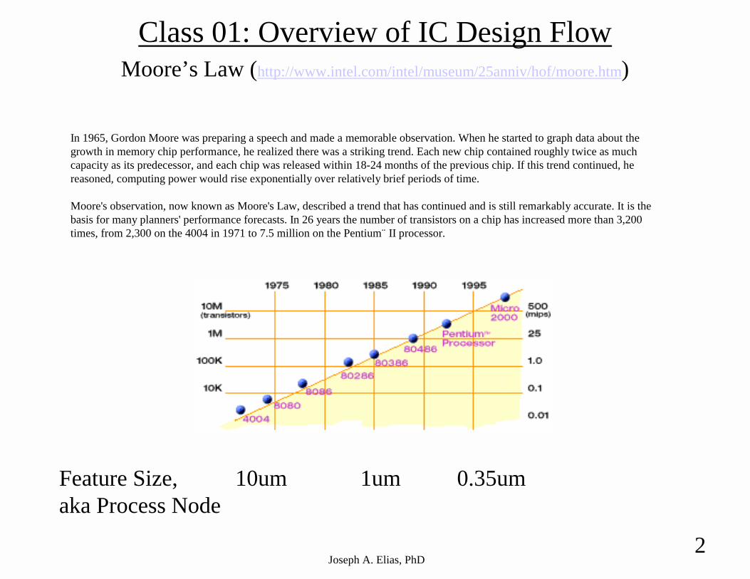
In 1965, Gordon Moore was preparing a speech and made a memorable observation. When he started to graph data about thegrowth in memory chip performance, he realized there was a striking trend. Each new chip contained roughly twice as muchcapacity as its predecessor, and each chip was released within 18-24 months of the previous chip. If this trend continued, hereasoned, computing power would rise exponentially over relatively brief periods of time.
Moore's observation, now known as Moore's Law, described a trend that has continued and is still remarkably accurate. It is thebasis for many planners' performance forecasts. In 26 years the number of transistors on a chip has increased more than 3,200times, from 2,300 on the 4004 in 1971 to 7.5 million on the Pentium¨ II processor.
10um 1um 0.35um
Moore’s Law (http://www.intel.com/intel/museum/25anniv/hof/moore.htm)
Feature Size,aka Process Node
Joseph A. Elias, PhD3
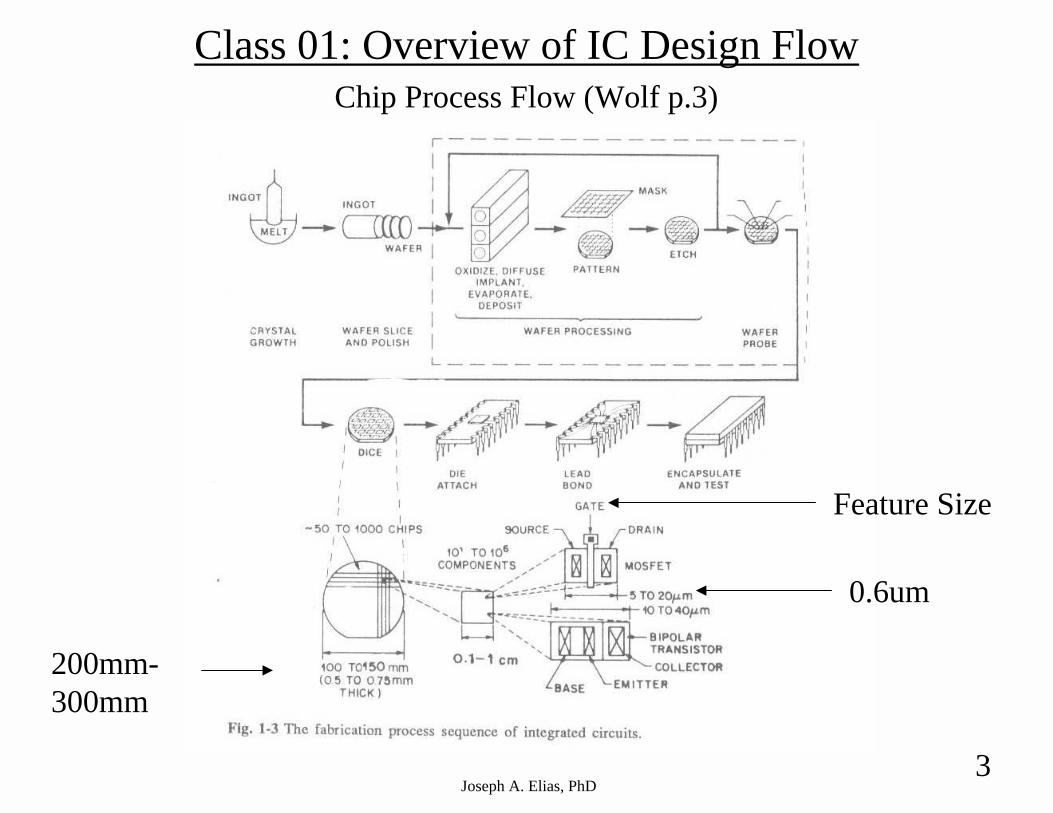
Class 01: Overview of IC Design FlowChip Process Flow (Wolf p.3)
Feature Size
200mm-300mm
0.6um
Joseph A. Elias, PhD4
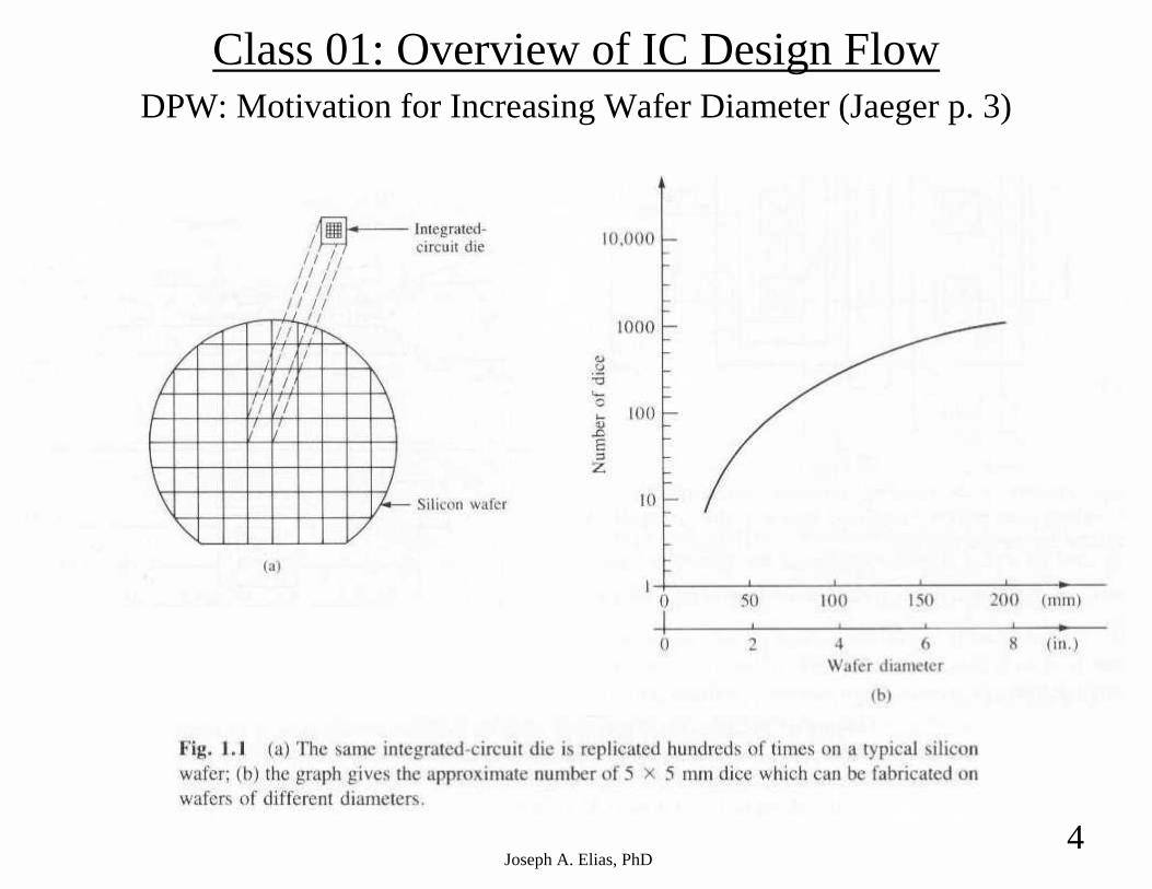
Class 01: Overview of IC Design FlowDPW: Motivation for Increasing Wafer Diameter (Jaeger p. 3)
Joseph A. Elias, PhD5
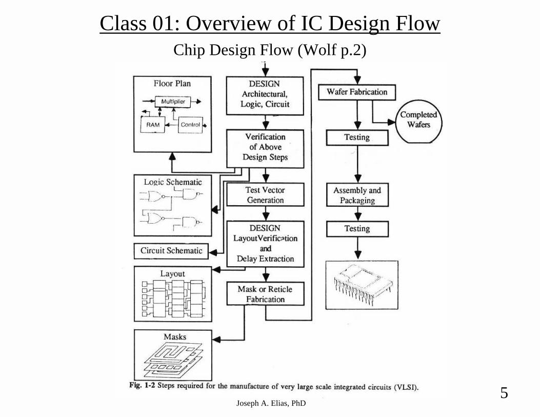
Class 01: Overview of IC Design FlowChip Design Flow (Wolf p.2)
Joseph A. Elias, PhD6
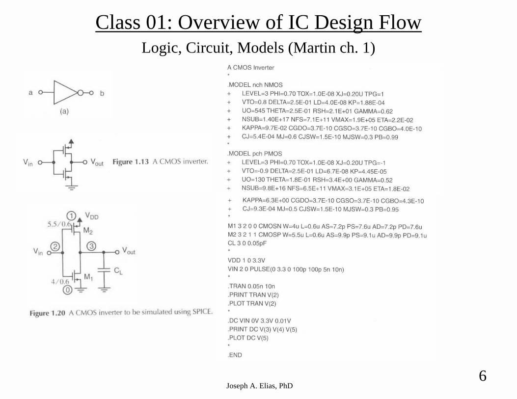
Class 01: Overview of IC Design FlowLogic, Circuit, Models (Martin ch. 1)
Joseph A. Elias, PhD7
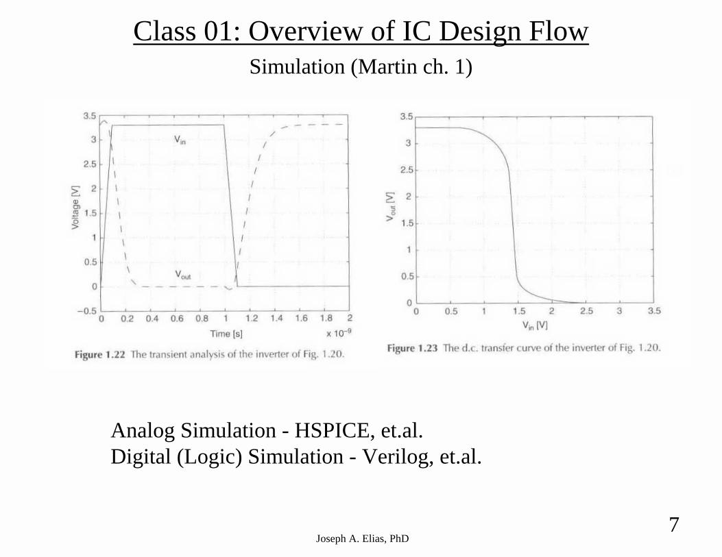
Class 01: Overview of IC Design FlowSimulation (Martin ch. 1)
Analog Simulation - HSPICE, et.al.Digital (Logic) Simulation - Verilog, et.al.
Joseph A. Elias, PhD8
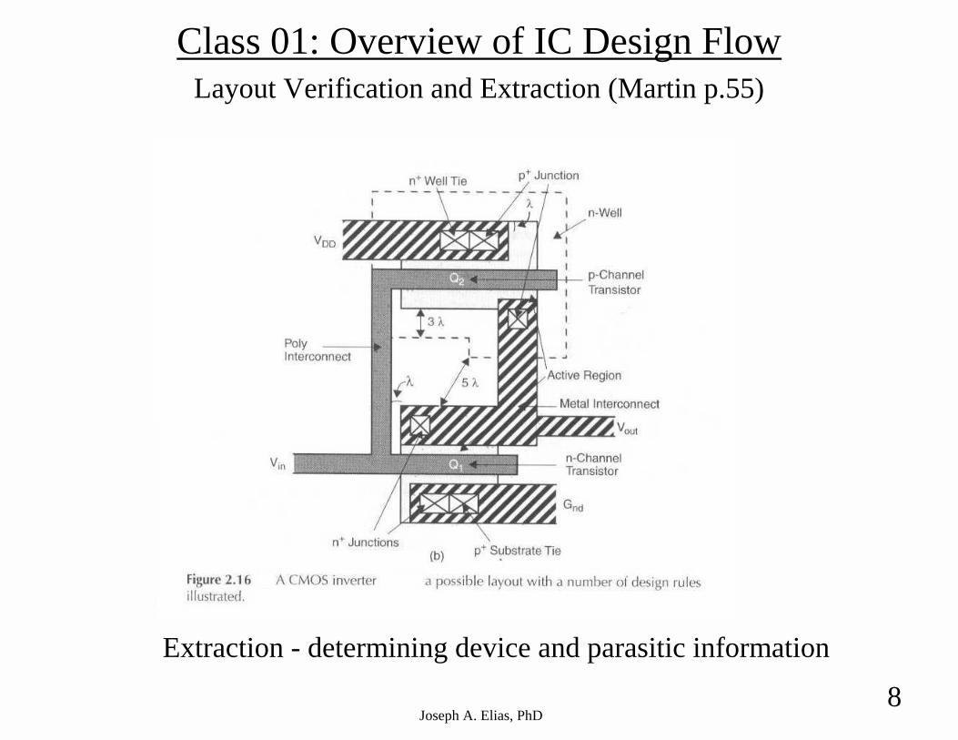
Class 01: Overview of IC Design FlowLayout Verification and Extraction (Martin p.55)
Extraction - determining device and parasitic information
Joseph A. Elias, PhD9
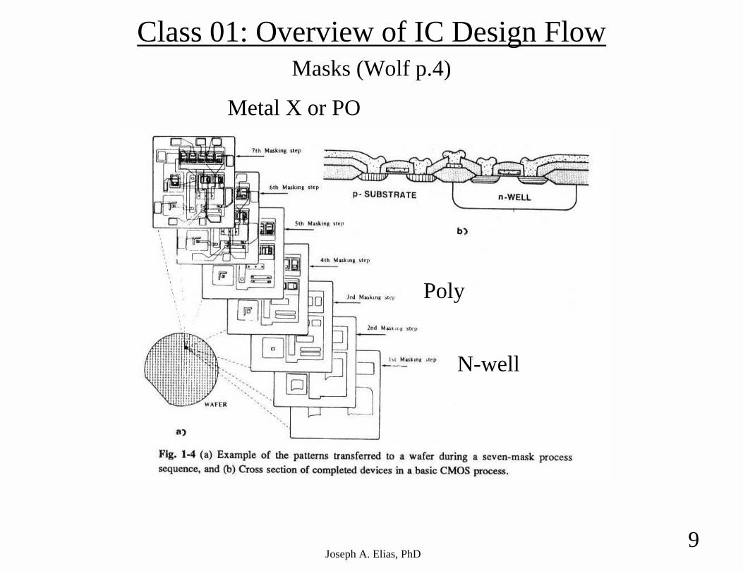
Class 01: Overview of IC Design FlowMasks (Wolf p.4)
N-well
Metal X or PO
Poly
Joseph A. Elias, PhD10
Class 01: Overview of IC Design FlowTesting (from experience)
In-Line Tests (Oxide Thickness, Poly Gate Width, Metal Sheet Resistance)Parametric Tests (Ids, Vt, Tox, Gm, CT resistance, Comb/Serpent Yields)Functional Tests (Memory Array R/W/E, Logic Patterns)Product Tests (Full Speed, High Temp)Qualification Testing (ESD, Latchup, Reliability, Package)Customer System Tests (In-board testing)