Embed Size (px)
Citation preview

Chapter 19N
Class 19: Micro I
REV 0; July 25, 2010.
Contents
19NClass 19: Micro I 119N.1A Little History . . . . . . . . . . . . . . . . . . . . . . . . . . . . . . . .. . . . . . . . . . . . . . . . . . . . . . . . 2
19N.1.1Prehistory: before the microprocessor . . . . . . . . . .. . . . . . . . . . . . . . . . . . . . . . . . . . . . . . . 219N.1.2The First Microprocessors . . . . . . . . . . . . . . . . . . . . .. . . . . . . . . . . . . . . . . . . . . . . . . . 319N.1.3Microcontrollers . . . . . . . . . . . . . . . . . . . . . . . . . . . .. . . . . . . . . . . . . . . . . . . . . . . . 319N.1.4Recalling What we Mean by “A Computer” . . . . . . . . . . . .. . . . . . . . . . . . . . . . . . . . . . . . . . 419N.1.5Stored Program Machine . . . . . . . . . . . . . . . . . . . . . . . .. . . . . . . . . . . . . . . . . . . . . . . . 4
19N.2Elements of a minimal machine . . . . . . . . . . . . . . . . . . . . .. . . . . . . . . . . . . . . . . . . . . . . . . . . 519N.2.1“Bootstrap” Loading . . . . . . . . . . . . . . . . . . . . . . . . . .. . . . . . . . . . . . . . . . . . . . . . . . 619N.2.2Microprocessor versus Microcontroller, again . . .. . . . . . . . . . . . . . . . . . . . . . . . . . . . . . . . . . 7
19N.3Why we Make You Work so Hard, on the Dallas Path . . . . . . . .. . . . . . . . . . . . . . . . . . . . . . . . . . . . . 819N.3.1. . . Why use the 8051? . . . . . . . . . . . . . . . . . . . . . . . . . . .. . . . . . . . . . . . . . . . . . . . . . 9
19N.4Rediscover the micro’s control signals. . . . . . . . . . . .. . . . . . . . . . . . . . . . . . . . . . . . . . . . . . . . . . . 919N.4.1. . . and Apply the control signals . . . . . . . . . . . . . . . .. . . . . . . . . . . . . . . . . . . . . . . . . . . . 1119N.4.2Doing the same thing with an 8051 . . . . . . . . . . . . . . . . .. . . . . . . . . . . . . . . . . . . . . . . . . . 13
19N.5Some Specifics of Our Lab Computer: Dallas Branch . . . . .. . . . . . . . . . . . . . . . . . . . . . . . . . . . . . . . 1519N.5.1Von Neumann versus Harvard Class . . . . . . . . . . . . . . . .. . . . . . . . . . . . . . . . . . . . . . . . . . 1519N.5.2Address Multiplexing . . . . . . . . . . . . . . . . . . . . . . . . .. . . . . . . . . . . . . . . . . . . . . . . . 1519N.5.3The Single-step Logic . . . . . . . . . . . . . . . . . . . . . . . . .. . . . . . . . . . . . . . . . . . . . . . . . 16
19N.6The First Day on the SiLab Branch . . . . . . . . . . . . . . . . . . .. . . . . . . . . . . . . . . . . . . . . . . . . . . . 18
1

2 Class 19: Micro I
Microcomputer Basics
19N.1 A Little History
19N.1.1 Prehistory: before the microprocessor
19N.1.1.1 Very Early Programmable Computers
Yes, there was a time when computers roamed the earth, but were not based on microprocessors. In the1930’s electromechanical computers were built, using relays; some were true “Turing machines,” fully pro-grammable. At the same time, the last, giant analog computers were growing, unaware that their era wasending (notably, Vannevar Bush’s differential analyzer, built in the late 1920’s at M.I.T.). The first fully-electronic computer, using vacuum tubes, was put into operation around 1943. It wasbig (see photo, below),and could run at first a few hours between disabling tube failures, later—with better tubes and the expedientof never turning the machine off—for about two days between failures. But it was fast—about 1000 timesfaster than its electromechanical predecessors.
Figure 1: ENIAC: the first fully-electronic computer (From W ikipedia; originally U.S. army photo:public domain)
19N.1.1.2 A Processor on a Circuit Board
Transistors relieved the painful difficulty caused by vacuum-tubes’ short lifetime. Integrated circuits madedigital circuitry much denser and cheaper than it had been. Below is a Data General Nova computer’s proces-sor board, ca. 1973. The board is about sixteen inches square, and is implemented with small- and medium-scale TTL IC’s. Note the afterthoughts implemented with hand-wired jumpers. (This was a production board,not just a prototype.)
Figure 2: Processor on a PC Board: Nova computer, ca. 1973

Class 19: Micro I 3
19N.1.2 The First Microprocessors
Intel produced a 4-bit processor called the 4004 in 1970. It was not conceived as a general purpose device,having been designed for a single customer that manufactutoimplement a calculator for a single customer.Intel gave it more general powers, but no one took much interest. In the beginning, there was the Intel 8080(1974). Well, this was the beginning in that the 8080 was the first successful microprocessor. It used an 8-bitdata bus and improved on the 8008, born in 1972 and not widely adopted; it had 18 pins, dissipated a Watt,and cost $400. The 8008 had, in turn, improved upon its 4-bit predecessor the 4004, launched in 1971 toimplement a calculator. The 8008 had not been widely adopted; it had 18 pins, dissipated a Watt, and cost$400. The early processors found their way into a few games, notable PONG1). The 8080 requiredtwentyother chips to implement its interface to the rest of the computer.
Meanwhile, competition was hot among the fancier parts, themicroprocessors—the brains of full-scale per-sonal computers: in 1976, defectors from Intel moved acrossthe street and formed Zilog, which put out theZ80 (so-called because it was to bethe last word in 8080’s); as often happens, it did not displace the inferiordesign. The next year, Apple launched the Apple II computer,its first mass-produced model, using a 6502processor, made by a small company named MOS Technology. In 1979, Intel’s 8086 became the industryleader by getting itself designed into the IBM PC, even though Motorola’s new 68000 was a much classierprocessor (adopted in the underdog Macintosh computers).
Below is a ’386motherboard2
Figure 3: IBM PC motherboard (’386/87 processor), ca. 1990)
19N.1.3 Microcontrollers
In order to make the micro practical for low-cost applications, it was necessary to integrate more onto onechip. Just as the processor moved from board to IC when it became “micro,” the entire computer moved fromboard to IC when it became a “microcontroller,” a self-sufficient computer (though typically a very simpleone).
The firstmicrocontroller, the Intel 8048 was born in 1976, just a few years after the first microprocessor.Given the history of computers, this is not surprising. It was not hard to envision a one-chip device that mightrun a small game; the surprise, for the world, was the rapid spread of the “personal computer.” Very fewpeople envisioned any need for such a gadget. At first it was only a few hard-core hobbyists who thoughtthey needed to own a home computer.
1PONG was a huge hit—even though its designer scorned it. He said that after the failure of a more complex game, he de-cided to “build a game so mindless and self-evident that a monkey or its equivalent (a drunk in a bar) could instantly understandit.” [see Michael Malone, The Microprocessor[:] A Biography (1995), p. 137, quoted by Sandra Woolley, U. of Birmingham, ateee.bham.ac.uk/wooolleysi/teaching/microhistory.htm].
2The motherboard is the printed circuit into which peripheral cards and memory could be plugged. A bare motherboard was acomputer, but not a useful one, as it might lack such essentials as a video display driver and would lack a mass storage device such as adisk drive.

4 Class 19: Micro I
The 8051, with onboard EPROM, was born in 1980, and sold in huge volume: 22 million in the first year3.Two years later, Motorola brought out the 6805, the best-selling microcontroller of its era (about 5 billionsold by the year 2001). Motorola remained for many years the market leader incontrollers, though not inprocessors, primarily because it dominated the growing automotive market. Later companies now outsellboth these original giants, in themicrocontroller market (Renesas—a Hitachi company— and Microchip, forexample, outsell Motorola, as of the date of this writing).
Of course, microcontrollers keep getting more and more micro. The largest of the packages below is theone you will meet in Lab 18, a wide-DIP 8051. Smaller packagesare shown, most of them happen to be inMicrochip’s “PIC” series.
Figure 4: Shrinking microntrollers: 8051 in wide DIP, HC05 in standard DIP package—and PIC’s small and smaller
[SOURCE OF THIS PIC IMAGE?]
19N.1.4 Recalling What we Mean by “A Computer”
The computers we are accustomed to are “Turing machines,” state machines that advance, one step at a time,from state to state, following a sequence and taking actionsin response to each successive instruction. Allthis is so familiar to you that attempting to describe this behavior may obscure it rather than illuminate itfor you. At the time when Turing described such behavior (1936), he was proposing not the design of amachine but a thought experiment that would help to define thelimitations of computing machines. Mostcontemporary computers are also Von Neumann designs—meaning that they use a single store for both dataand instructions; but the alternative arrangement—called“Harvard class”—is also used (and even happensto be the scheme envisioned by the designers of the processorthat we use in these labs, the 8051). Harvardarchitecture places instructions and data in separate stores. In our lab computer, as you soon will see, weimpose the more conventional design on the 8051, despite itsdesigners’ intentions. More on this, later.
19N.1.5 Stored Program Machine
The processor is astate machine (short for “finite state machine”) within astate machine: the computer itselfis a state machine. It reads, from memory, one instruction ata time, executes it, then goes back to memory tofind out what to do next4. The sequence of instructions form aprogram (or “code”), stored in memory.
The processor, the brains of the computer, is itself a smaller-scale state machine. It is fed “instructions”—8-bit codes, in our case—that tell it which of its several tricks to do (in principle,28 tricks). Here’s a diagramshowing an “instruction decoder” in the usual form used to describe state machines:
3Ibid.4Most processors use apre-fetch or pipeline to get one or more further words from memory, while busydecoding the current
instruction. The 8051 does this, ancient though its design may be!

Class 19: Micro I 5
Figure 5: processor asstate machine; it is the brains of the larger state machine that is the computer
As it executes each trick—stepping through a multi-clock sequence of states—it can turn on 3-states so as todrive signals here or there, can clock registers so as to catch signals, and so on.
19N.2 Elements of a minimal machine
An ordinarymicroprocessor requires a good deal of support in order to do anything useful: in order to form a“microcomputer.” It needs memory, at very least. And it needs some sort of I/O (input/output), to do anythinguseful. Here’s a block diagram of a generic computer:
Figure 6: Any computer: which elements are essential?
Which of these elements are required, which optional? Couldone omit RAM? ROM? A disc drive? Key-board? Display? (Surely we could omit ADC and DAC.) Yes, we could omit any of those elements, thoughnot all.
• RAM: RAM is important for general-purpose computers, but isnot required for a dedicated controller.RAM holds program code, as well as data, and both normally areloaded from an external disc drive(if memory becomes inexpensive enough, the era of spinning drives will at long last end). But RAM isnot required for a controller dedicated, for example, to running a vending machine. (Yes, the machine

6 Class 19: Micro I
needs to be able to remember short-term variables; but the amount of memory needed for this purposemay be so small that it can better be called “registers.)
• ROM: ROM allows a computer to run on startup—before any code has been loaded into RAM from anexternal store. Once upon a time, before ROM, a computer lostall its code on power-down, and had tobe nursed back to life, when turned on. Here is the front panelof the old Nova computer that we onceused daily.5
Figure 7: Front panel of a DEC Nova computer (born 1969)
Why all those toggle switches? They were used to enter, a wordat a time, instruction codes. Putenough in, and you could then run the little program that readin a larger program from the paper tape.
19N.2.1 “Bootstrap” Loading
It’s a bit hard to imagine working with such a machine (havingpaid about $8000 for it): startup waslaborious. It’s for that reason that the computer that just ran when you turned it on seemed almostmiraculous: it appeared to be doing the impossible feat of lifting itself up by its own bootstraps:
Figure 8: Miracle of the 1960’s: cowboy, like computer, lifts himself by bootstraps
Hence the term “bootstrap loading,” now shortened to “booting” of the computer, to mean “startingup,” or (more specifically) “loading operating system.”
• I/O: Yes, there must be some sort of input/output hardware, if the computer is to accomplish anything;but no particular form is required. General-purpose computers use keyboards and visual displays, but acontroller regulating a process might conceivably get by with ADC and DAC, and perhaps a few knobs(read by the ADC).
5Source: Wikipedia: http://upload.wikimedia.org/wikipedia/commons/5/58/Nova1200.agr.jpg Used under Gnu GPL license.

Class 19: Micro I 7
19N.2.2 Microprocessor versus Microcontroller, again
Figure 9: Microprocessor plus stuff = computer; one-chip⇒ Microcontroller
If you take theDallas path, your lab computer will look like the big, messy diagramon the left in fig. 9—andlike the big, pretty-messy circuit boards in fig. 10:6 processor plus memory plus I/O devices, and the gluelogic to make this all work. But the brains of your computer—the processor–is in fact amicrocontroller (itsgeneric name is ‘8051,’ but you will use one of many variants on Intel’s basic design, a version designed byMaxim/Dallas Semiconductor).
Even better than a block diagram, photographs of the two alternatives—the breadboarded computer you arein the process of building versus a single-chip microcontroller—show how very tidy and dense the controllercircuit is (and the controller shown is housed in an unusually large package):
Figure 10: Breadboarded lab computer: lots of parts, lots ofwiring
Once you are satisfied with something you have built and programmed with your lab computer, you can,if you like, pull the DS89C420/430 out of the circuit, and letit run by itself (you’d need to add only acrystal to provide the clock signal). This is what we did whenwe needed a liquid crystal display for the labmicrocomputer. A piece of that circuit board, showing the 8051, appears in fig. 11.
Figure 11: A microcontroller circuit can be self-containedand tidy
6Well, these actually are unusually tidily-wired. But it’s very hard to breadboard a truly tidy circuit on this scale.
8 Class 19: Micro I
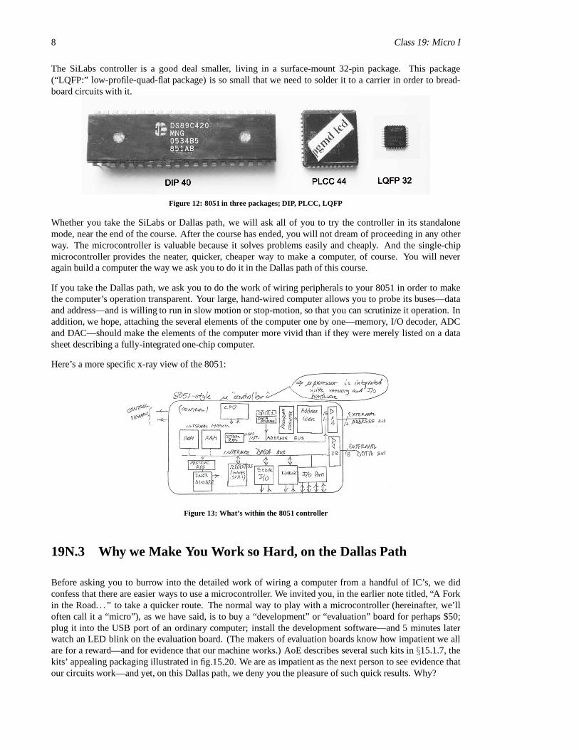
The SiLabs controller is a good deal smaller, living in a surface-mount 32-pin package. This package(“LQFP:” low-profile-quad-flat package) is so small that we need to solder it to a carrier in order to bread-board circuits with it.
Figure 12: 8051 in three packages; DIP, PLCC, LQFP
Whether you take the SiLabs or Dallas path, we will ask all of you to try the controller in its standalonemode, near the end of the course. After the course has ended, you will not dream of proceeding in any otherway. The microcontroller is valuable because it solves problems easily and cheaply. And the single-chipmicrocontroller provides the neater, quicker, cheaper wayto make a computer, of course. You will neveragain build a computer the way we ask you to do it in the Dallas path of this course.
If you take the Dallas path, we ask you to do the work of wiring peripherals to your 8051 in order to makethe computer’s operation transparent. Your large, hand-wired computer allows you to probe its buses—dataand address—and is willing to run in slow motion or stop-motion, so that you can scrutinize it operation. Inaddition, we hope, attaching the several elements of the computer one by one—memory, I/O decoder, ADCand DAC—should make the elements of the computer more vivid than if they were merely listed on a datasheet describing a fully-integrated one-chip computer.
Here’s a more specific x-ray view of the 8051:
Figure 13: What’s within the 8051 controller
19N.3 Why we Make You Work so Hard, on the Dallas Path
Before asking you to burrow into the detailed work of wiring acomputer from a handful of IC’s, we didconfess that there are easier ways to use a microcontroller.We invited you, in the earlier note titled, “A Forkin the Road. . . ” to take a quicker route. The normal way to playwith a microcontroller (hereinafter, we’lloften call it a “micro”), as we have said, is to buy a “development” or “evaluation” board for perhaps $50;plug it into the USB port of an ordinary computer; install thedevelopment software—and 5 minutes laterwatch an LED blink on the evaluation board. (The makers of evaluation boards know how impatient we allare for a reward—and for evidence that our machine works.) AoE describes several such kits in§15.1.7, thekits’ appealing packaging illustrated in fig.15.20. We are as impatient as the next person to see evidence thatour circuits work—and yet, on this Dallas path, we deny you the pleasure of such quick results. Why?

Class 19: Micro I 9
We can offer several reasons. One is that we think it’s satisfying to build a machine with a minimum ofmysterious magic humming behind the scenes. Your little computer will include no clever operating system,nor even a “monitor” program; it will know no tricks that you don’t teach it. (The processor itself, we shouldadmit, will remain a black box; we didn’t have the nerve to askto build a processor from gates and flops.Buiding up a processor could, in itself, occupy a good part ofa course.)
A second reason—somewhat distinct from the goal of minimizing magic—is that we want to make thenormally-opaque computer more nearly transparent, as it runs: the circuit you will build displays its ac-tivity on the twobuses—address anddata. At full speed, such activity would be an unintelligible, but asyou single-step through code7 you can scrutinize all the machine’s signals at your leisure. Hardware freezesexecution until your are ready to proceed. We think this close look at the machine’s operation will makenotions like memory-addressing and instruction pre-fetchno longer just abstractions.
A third reason, related but again distinct, is that we are giving you a wealth of opportunities tomake mistakes.That may not sound like a gift that you want, but when we say, facetiously, in the Worked Example titled“A Garden of Bugs,“ that bugs are our most important product,we say it with some pride. You have beendebugging the circuits that you build, all through this course. But this micro circuit, with its 400 to 500connection points, will present harder puzzles than the earlier, smaller circuits.
19N.3.1 . . .Why use the 8051? AoE§15.1.2
The original 8051 design is older than almost any of our students.8 There are faster devices with morefeatures and more peripherals—though the Silicon Labs version of the 8051 includes a pretty rich collection ofperipherals, including ADC’s and DAC’s (see AoE fig.15.7). We chose the 8051 because it is the most widely-sourced design (that is, it is made by a great many manufacturers); you will find it offered, for example, as aprocessor module that can be loaded into an FPGA (8051 “cores” from Cast or Hitech Global, can be loadedinto Xilinx and other FPGA’s) and you will see it included within a programmable “analog front end” ICfrom Analog Devices (ADuC842).
The 8051 is a classic, among microcontrollers, illustrating much that you will find in any other controller thatyou meet. Some of its quirks reflect its age: its restricted off-chip addressing modes, for example, and thefact that all off-chip data must pass through the accumulator register.
When operating upon on-chip registers, the 8051 is much lessquirky—and this is the way a controller or-dinarily is used. The SiLabs branch of our microcontroller labs work that way.9 The 8051 remains a livelydesign—including some innovations that have not yet reached other processors, like SiLabs’s controller thatruns from the startlingly-low supply voltage of 0.9V. And wehope that even if your next controller is a morerecent one, its architecture will look familiar, since it derived from the design of this, the original microcon-troller.
19N.4 Rediscover the micro’s control signals. . .
All happy processors are alike, more or less: their control signals resemble one another’s. Each unhappycomputer is unhappy in its own way—this you will discover as you debug your breadboarded lab computer,and debugging is a large part of the fun and challenge of putting together this machine. We have written
7“Single-step” in your computer means “execute one bus-access at a time.” This is a slightly finer-grained single-step than the moreusual meaning of single-step: “execute one instruction at atime.”
8It is the original 8051 design that is old. The versions of the 8051 that we use, from Dallas/Maxim and from SiLabs, are muchyounger.
9The sole exception, the single case where the SiLabs programs run ‘off chip’ is the program that stores data in MOVX RAM. Eventhis is, in fact,on chip, but the addressing mode is the same as for true off-chip accesses, and partakes of the oddnesses of that mode.Address must be provided by a dedicateddata pointer register, most notably.

10 Class 19: Micro I
some notes recording standard debugging techniques, and a few common problems we have seen in this labcomputer (“Garden of Bugs. . . ”). Here, we invite you to rediscover the control signals that any old processorwould need, in order to communicate with the devices attached to it.
The processor is the boss, or the conductor of the orchestra (or, maybe it’s only a chamber group; not so manyelements, in our examples). It determines when each event should occur, and sends out signals to make theseevents occur. The processor must say what sort of operation it means to do, with whom it wants to do it,and exactlywhen. We’ve listed the elements of information that seem required—and alongside these genericdescriptions, we’ve listed the signals used by three processors or bus standards:
• the old IBM PC 16-bit ISA bus—now gone from desktop machines but persisting in industrial com-puters in the PC104 standard;
• the 8051 controller/processor’s signals—when used, as in our lab computer—to control an external bus10;
• Motorola’s classic 68000 processor11, to illustrate another way to handle timing signals.AoE§14.4.1
Kind of Information ISA bus 8051 68000Direction of transfer MEMR*,MEMW*,IOR*,IOW* RD*,WR* R/W*Timing included included Data Strobe*, Addr Strobe*Category: Mem vs I/O included doesn’t care doesn’t care
. . . but we care, so we can assign
. . . an address line to distinguish
. . . mem from I/O (we use A15)Which, Address: 20 lines Addr: 16 lines Addr: 32 lineswithin category (10 lines for I/O) (15 if we’ve used 1)
We don’t expect you to digest all this information from a dense table. Let’s note, more informally, some ofwhat this table has to say. All these processors and buses agree concerning what needs saying.
• Direction: “Direction of transfer” describes which way information is flowing: toward the CPU oraway. By rigid convention, the description isCPU-centric:
– RD* (“read,” and active-low, as usual) meanstoward the CPU;– WR* meansaway from the CPU.
Figure 14: CPU-centrism defines the otherwise ambiguous “Read” and “Write”
ISA and 8051 use very similar signals—not so surprising whenone recalls that Intel provided theprocessors behind both schemes, with names like RD* or WR*. Motorola did it differently: theyprovided adirection signal, R/W*12 That R/W* signal includesno timing information at all.
• Timing: the ISA and 8051 signals include the timing with other information: the beginning or end ofthe signal (sometimes both, but not always) indicateswhen the action occurs. When RD* goes low,for example, that means the processor wants a peripheral or memory to turn on its 3-state driver; whenRD* goes high again, that’s the time when the processor will pick up the data that was provided.
10Bringing out the buses is decidedly not standard behavior for a microcontroller.11This processor, once the brains of Macintosh computers among others, is a 16-bit processor. It is still in production (byFreescale,
not Motorola), but it has been largely superseded by 32-bit processors.12As you’ve gathered, by now, such a signal indicates, in its naming, which level signals which activity. A low on R/W* indicates a
write, for example.

Class 19: Micro I 11
Figure 15: A “RD*” pulse, for example, says not onlywhat the processor is doing, but alsowhen
The Motorola scheme is different. They provide a separate timing pulse— called “strobe,” as puretiming signals often are. Two lines are used to say the equivalent of the 8051’s RD*: R/W* high, andDS* (data strobe) asserted low. The Motorola scheme has its partisans (it doesn’t waste lines, becausestrobes can be shared); both schemes work.
• Memory versus I/O: this distinction is useful to us humans.
Memory is what it sounds like; I/O is everything that is not memory—even devices like keyboards anddisplays, which you may think of as essential to a computer are I/O.
But whether the processor or bus needs to distinguish the twodepends on whether it wants to be ableto operate on them differently. The ISA bus does distinguishthe two, and this allows it to require feweraddress lines for I/O devices (10) than for memory, easing the hardware designer’s work somewhat. The8051 has no special I/O operations or restrictions; anything it can do to something stored in memory itcan do to a peripheral as well. We make the distinction, in ourlab computer, because it is convenient forus to doextremely simplified I/O decoding (since we have few I/O devices), while preserving normaltreatment of memory (where we have 32K locations to access).We do what the ISA bus does—in anextreme form.
• Which, within a category: Address lines are used, by all. Theold ISA bus handicapped itself, longago, by providing too few lines for a full-scale computer (16lines), and had to devise clumsy waysto enlarge the addressed space (“paging” among 64K blocks).The 8051 is similarly constricted, andnew variants offer paging to expand the available space. Motorola’s 68000 started big, having modeleditself on larger minicomputers: 32 lines define a large address space, even by present standards.
19N.4.1 . . . and Apply the control signals
Let’s try applying these control signals, for the ISA and 8051 cases, to attach a simple peripheral, an 8-bitpair of hexadecimal displays as output device. The hardwareis utterly simple: just a pair of displays withbuilt-in latches:
19N.4.1.1 ISA bus case AoE§14.2.6
Let’s choose appropriate ISA bus signals, first. The operation is anOUT—the I/O version of a WRITE—since the flow of information is away from the CPU. So, we want one of the twowrite’s. This is not a memoryoperation, so we need IOW*. That takes care of most of the task: this signal defines direction, timing and I/Oversus memory. All that remains is to place the display at a single location (so it doesn’t tread on the toes ofanything else in the computer), and then let the processor talk to it at that location.
When using a full-scale computer—like the old ISA-bus computer on which we tried this, as a demonstration—we need to take account of what already is installed on the computer, and find an empty slot where we can putthe new peripheral. The IBM PC we were using has some clear space beginning at hexadecimal address 300h,so let’s put it there. How do we “put it there?” All we mean is “let the peripheral detect when that addresscomes from the computer, and if it coincides with IOW*, generate an OUT300h* signal that will catch thedata that the CPU is sending to this peripheral. 300h is a twelve-bit number; but the ISA bus specifies that

12 Class 19: Micro I
only 10 address lines are used to define an I/O address. So, we need decode only 10: A9. . .A0. In binary,then, the address 300h will look like;
A9..A0: 11 0000 0000
That is the pattern our logic needs to detect. So, all we need is a wide AND gate that will combine this bitpattern with an assertion of IOW* (and a pesky additional signal, AEN, which we want to make sure isnotasserted, because it indicates an exceptional sort of operation, “Direct Memory Addressing” (DMA)).
Here’s a timing diagram describing the bus behavior we can expect (this appears also in AoE fig.14.7):
Figure 16: Timing diagram for ISA bus write
The diagram tells us we should use the later,trailing edge of the IOW* pulse, not the leading edge. Put thesignals together, into a wide AND gate (probably using a PAL), and it’s done:
Figure 17: Display I/O decoding for ISA bus
Address Decoding; a bus example We implemented this simple address decoding in a PAL, bringing outone extra line—AddressMatch—to indicate less than a complete decode. We ran a littleBasic program on thePC, putting out incrementing bytes to port 300h, and then watched on the oscilloscope, triggering differentlyeach time. The results reveal some truths about not just thisold PC but about computers, generally.
Figure 18: ISA bus signals as increment-display program loops
Let’s take the three cases one at a time:

Class 19: Micro I 13
• Case a), on the left (triggering on IOW*).
We see an overlay of wider and narrower IOW* pulses, and faintghosts of Address Match (300h) andof OUT300h, implying that only a few of the cases where IOW* isasserted coincide with the latter twosignals—though the faintness of the traces makes it impossible to be sure of that. Why might there beIOW*’s that don’t coincide with the other signals? Because on a full-scale computer, the little programwe wrote to exercise this display is not the only program running. Some other, background program isdoing I/O writes, as well. So, only one of the IOW* signals isours.
• Case b) (triggering on Address Match)
We took care to see that nothing else is installed at I/O address 300h. But we see 300h matches that donot coincide with IOW*—and in this case there is not even a faint IOW* trace, suggesting thatmost300h instances are not ours. Hw can this be? There are two short answers available: first, 300h canoccur in memory space as well as I/O, and for those cases therewill be no assertion of IOW*. Second,our detection of 300h looks at only the low ten bits, of twenty. So the matches in memory space canoccur for any 20-bit address that ends in 300h. Now, perhaps,the multiple address matches don’t seemso strange.
• Case c) (triggering on OUT300h*)
At last things are simple again: the 3 signals line up nicely:IOW* coincides with address 300h andgenerates OUT300h*, as planned. The bottom trace, showing line 5 of the data bus, appears bothlow and high during the OUT300h pulse. This makes sense, too,if we assume that we are seeingseveral scope traces overlaid, once more: the incrementing-value program causes any single bit of theincremented value to toggle. So, D5 is sometimes recorded high, sometimes recorded low.
What is the rest of the activity of this very busy data line? The waveform is complicated—but appears atleast to be constant in this rightmost case. The other two cases look pretty chaotic, and show sometimesramps rather than good logic levels. The major point we want to underline, here, is thatmost ofwhat travels on the data bus is not data—at least, not data in the strict sense. Instead, most trafficisinstructions, in a conventional Von Neumann machine like this ISA bus computer—where instructionsand data (in the narrow sense) live alongside each other in a common memory, and travel on thecommon bus. We’ll see in a moment that our little lab computershares this conventional design. Theodd ramps show the cases where the line is not driven high or low but is 3-stated: no one is driving itat all, so it drifts toward a level close to the midpoint of thelogic range (the displays, at least, tend todraw it there, as they are TTL-like).
19N.4.2 Doing the same thing with an 8051
In some ways, the task we just asked the ISA bus to do is more easily done with an 8051. It is easier becausein our small 8051 world there is no need to consult a table thatindicates what uses other designers of hardwareand code have made of available addresses. Things can be verysimple, if we like; we are in charge. For thepresent example, let’s put the data display at a port we call “Port zero”—using the external buses; and let’sdecree that we need to distinguish Port zero from only one other port, Port one. Let us, further, adopt theconvention we use in our lab computer, assigning memory to the lower half of all address space, I/O to thehigher half. Thus:

14 Class 19: Micro I
Figure 19: We split address space equally between memory andI/O, to keep things simple
A15, then, distinguishes I/O from memory, and “Port zero” isjust the first I/O location.
To decode Port zero, we need to find the appropriate 8051 control signals, and a few address lines. Here arethe candidate 8051 control signals, once again:
Here is a reminder of the relevant 8051 signals:
Figure 20: 8051 control signals
The msb of the address lines, A15, we have decided, will mean “I/O” when high. Since this is anoutputoperation, in which information flows from CPU to the world, it is a write, and WR* is the appropriatecontrol signal. Now all that remains is to distinguish port number “zero” from port number “one.” Theobvious way to distinguish “zero” from “one” is to use the least-significant address line, A0 (and it would beperverse to use any wayother than the obvious way; we would only confuse people who used our machine).So:
Figure 21: Decoding an OUT0* port for a tiny 8051 controller
How many other ports does this decoding permit? Well, we can have a Port one by detecting A0high. Wecan also make use ofinput ports at the same two addresses—IN0* and IN1*. So, our decoding permits fourports, two IN, two OUT (or, if you prefer, “two bidirectionalports”). This arrangement would not let ourcomputer do much; even our small lab computer will want twiceas many ports. But this simple examplebegins to let one feel how simple our decoding can be (“lazy” is what we call this sort of decoding—were wedeliberately omit many address lines, in order to keep our hardware simple). We could define twice as manyports by adding a second address line (A1); and so on. Next time, we will do exactly that.

Class 19: Micro I 15
19N.5 Some Specifics of Our Lab Computer: Dallas Branch
We’re interested in the little lab computer as a device to introduce some general patterns in the behavior ofcomputers and microcontrollers. But along with these general truths—which reflect the similarities among allcontemporary computers—we’re obliged to get used to some very processor-specific details as well. Thesewon’t carry over to your next design, but are necessary to letyou understand this lab computer.
19N.5.1 Von Neumann versus Harvard Class
One might expect a computer born at Harvard to be a Harvard Class computer, but our Dallas design is not.In fact, we went slightly out of our way to make sure it was not.We should define our jargon, in case it’s notfamiliar to you. Some computers placeinstructions in a memory separate fromdata; most do not do this. Theones that separate the two are called “Harvard Class” machines13. This separation has been exceptional untilrecently, when microcontrollers (notably the PIC processors) have made this design choice more common.The 8051’s designers envisioned such a separation—but we have defeated that expectation, because we didn’twant to ask you to install two memories in your lab computer. (We also like to offer you a computer that isconventional in its design.)
The 8051 distinguishes acode fetch from a data read. PSEN* (“Program Store Enable*”) is intended toenable thecode memory; RD* should enable thedata memory. Yourglue PAL merges the two sorts ofmemory by simplyORing PSEN* with RD* in the RAM’s 3-state control, its OE* pin:
Figure 22: OR’ing PSEN* and RD* eliminates the “Harvard Class” distinction between code memory and data memory
19N.5.2 Address Multiplexing
The 8051, like most controllers, makes double use of some of its pins, so as to keep the package small (40pins in DIP14, 44 pins in the more compact PLCC15 and, consequently, inexpensive. The 8051 saves 7 pinsby making double use of 8 pins for both address and data—one pin is sacrificed to indicate what the 8 linesmean.
More specifically, early in every bus cycle16 these shared lines carry the 8 bits of low-order address. A shorttime later (about 80ns later, given the 11MHz clock that we use), those lines switch over to carrying the 8-bitsof data. The ALE signal (“Address Latch Enable”) serves to catch theaddress information in a latch, beforeit evaporates to be replaced bydata. Here’s the timing (at 11MHz)17:
13They got this name because this design was used in by Aiken’s Harvard Mark I, perhaps the world’s first automatic digital computer(1944).
14DIP, as you know, is Dual Inline Package—our usual breadboarding package.15PLCC is “Plastic Leaded Chip Carrier,” a relatively large package by today’s standards. It can be soldered as surface mounted or
housed in a socket.16Note that this multiplexing applies only when one uses the 8051 with external buses.17The latching shown is standard for the 8051. Some 8051 variants, like Dallas’ DS89C4x0 controllers, offer the option of latching
thehigh half of address rather than low; in most cases (within any 256-byte “page”), this allows faster bus accesses.

16 Class 19: Micro I
Figure 23: ALE latches multiplexed address information; these shared pins later carrydata
These shared or multiplexed lines are named “AD7. . .AD0.” This sounds like “Address. . . ”, but here “AD”means “Address/Data.” You may be puzzled, at first, by the circuit diagram showing these lines going to alatch, but also to what is labelled “Data bus:”
Figure 24: Common lines, AD0. . . AD7, briefly carry low-half address, then all data
But this complication is the price we pay for limiting the number of pins on the package. A few other pins,too, serve multiple functions; RST (normally an input, but an output during trouble that forces a system reset),PSEN* (normally an output, but input for the purpose of turning on the on-chip “loader” circuitry). But it isthe shared “AD” lines whose multiplexing you will work with every day.
19N.5.3 The Single-step Logic
As the Dallas micro-one lab notes explain, our little computer implements a single-step function entirely inhardware.18
Our hardware single-step for the Dallas circuit is simple: it works by sending out just a few clocks at a time,then choking off the clock source. It uses ALE to keep itself synchronized—so that it always stops abouthalfway through any bus access, at a time when all control, data and address signals are valid. That makesthis single-step very useful for debugging hardware. It also serves to let us debug small programs, by letting
18There are other ways to achieve single stepping: one can enable interrupts, then use a level-sensitive interrupt to break into programexecution after each instruction (see Intel’s “MCS51 Microcontroller’s User’s Manual,” p. 326). And more recent micro’s permitcontrol of execution from an external personal computer. This is the way we work with SiLabs 8051: a serial link from a PC allowssingle-stepping and allows interrogation of on-chip registers—a trick our little Dallas computer cannot do.

Class 19: Micro I 17
us execute their code one line at a time19. If, on the keypad, you select STEP rather than RUN, then eachtime you hit the INC button, the processor is fed enough clocks so that it proceeds about halfway through anoperation. (This operation may be an instruction fetch, or may be, for example, an input or output operation.)The STEP PAL does this by shutting off the processor’s clock soon after the ALE pulse that marks eachoperation. Here’s a scope image showing one such burst of four clocks, terminating soon after ALE; at thattime, the address has been caught in the ’573, and the multiplexed data lines are serving asdata bus.
19N.5.3.1 . . .Waveforms
Figure 25: STEP PAL allows single-step by cutting off clock soon after ALE (This figure appears also in lab micro 1.)
Most instruction cycles use four XTAL1 clocks20. But an instruction that takes substantial execution timewill use many more clocks. The single-step hardware, by always allowing two clock cycles after the fall ofALE, permits single-stepping regardless of the number of clocks used in a particular instruction.
19N.5.3.2 . . .Schematic
The general idea is simple; the implementation is fussy. To keep clocks intact, not shaved or (worse!) glitchy,the synchronizing flip-flops use the falling edge of the clock. Here’s an attempt to explain what’s going on21:
Figure 26: The single-step logic: the details
19“One line. . . ” is a little vague: strictly, it is one bus access at a time.20This is true for bus cycles using the external buses. When running from internal ROM, the processor executesmany of its instructions
in a single XTAL1 cycle. A further complication (not one you need to worry about): XTAL1, the clock input, is not necessarily thesame as the internal clock used by the controller. That internal clock may be a 2X or 4X multiple of XTAL1, stepped up by an on-chip“crystal multiplier” (see “Ultra-High-Speed Flash Microcontroller User’s Guide,” pp. 78-79).
21We know: it’s always hard to make sense of someone else’s peculiar design choices, or of someone else’s ingenious programcode!

18 Class 19: Micro I
19N.6 The First Day on the SiLab Branch
Using the SiLabs one-chip design (the ’410), you’ll have almost nothing to build, before you can try out someprograms. You need only make the connections from PC to controller, using a pin-sharing scheme that allowsdebugging control without making a permanent commitment ofany controller pins. With just 32 pins, thispin sharing makes good sense—and is preferable to committing four pins full-time, as in the more standardJTAG protocol.22 This proprietary serial link (which SiLabs calls “C2”) is detailed in a note called “. . .SiLabsIDE,” and more briefly in the SiLab micro 1 lab.
Since the lab includes next to no hardware work, you will be free to spend your energies getting used to theassembler, and to the debugging interface. You will find thatyou can watch the 8051’s registers as you singlestep. The first day’s program does no more than blink an LED—providing the pleasure that we have admittedeveryone seems to want from a controller.
(classmicro1 july10.tex; July 25, 2010)
22“JTAG” is “Joint Test Action Group,” the name of an industry group that established a standard way to test circuits by bringing theirinternal nodes to pins where levels can be read serially.


![rsuper Micro] 7 -e y 7-532-0035 rsuper Micro] Super Micro ...rsuper Micro] 7 -e y 7-532-0035 rsuper Micro] Super Micro E240 cojp sales@deptazett.cojp YoutubeTrazettJP ! r Super Micro]](https://img.pdfslide.net/doc/110x75/6107e5c6866d1d42da4aa8e4/rsuper-micro-7-e-y-7-532-0035-rsuper-micro-super-micro-rsuper-micro-7-e.jpg)