Embed Size (px)
Citation preview

Evaluates: MAX77752MAX77752 Evaluation KitClick here for production status of specific part numbers.
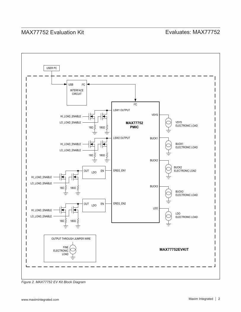
General DescriptionThe MAX77752 evaluation kit (EV kit) is a fully assembled and tested printed circuit board (PCB) that demonstrates the highly integrated MAX77752 PMIC. The MAX77752 comprises three buck converters, a low dropout linear regulator, two external regulators enable outputs, two dedicated load switch controllers, and an inrush-current limiter which can be configured as a third load switch controller using OTP.The EV kit also includes a MAXQ2000 microcontroller command module that provides the I2C interface to control power sequence, inrush current, individual output on/off, and setting regulator output voltage.The MAX77752 evaluation software is provided for easy evaluation.
Benefits and Features ● USB to I2C Converter Allows for Easy
Communication ● Level Translator (MAX3395) Allows for Adjusting
I2C Bus Voltage from 1.8V to 3.3V ● On-Board Electronics Load Allows for Easy
Evaluation• GUI Allows Static/Dynamic Load Adjustment for
Buck Converters, LDO, LSWs, and SYS• MOSFET can be Driven by External Function
Generator to Evaluate Transient Performance for Each Regulator
● Proven PCB Reference Design and Layout ● Fully Assembled and Tested
319-100088; Rev 0; 10/17
Ordering Information appears at end of data sheet.
Figure 1. MAX77752 EV Kit Photo
Maxim Integrated │ 2www.maximintegrated.com
Evaluates: MAX77752MAX77752 Evaluation Kit
Figure 2. MAX77752 EV Kit Block Diagram
INTERFACE CIRCUIT
USB
I2C
BUCK1
BUCK2
BUCK3
LDO
LSW1 OUTPUT
18Ω
HI_LOAD_ENABLE
LO_LOAD_ENABLE
LDO ENOUT
VSYS
VSYSELECTRONIC LOAD
BUCK1ELECTRONIC LOAD
BUCK2ELECTRONIC LOAD
BUCK3ELECTRONIC LOAD
LDOELECTRONIC LOAD
USER PC
MAX77752EVKIT
I2C
180Ω
LSW2 OUTPUT
18Ω
HI_LOAD_ENABLE
LO_LOAD_ENABLE
180Ω
EREG_EN1
18Ω 180Ω
HI_LOAD_ENABLE
LO_LOAD_ENABLE
LDO ENOUT EREG_EN2
18Ω 180Ω
HI_LOAD_ENABLE
LO_LOAD_ENABLE
MAX77752 PMIC
FINEELECTRONIC
LOAD
OUTPUT THROUGH JUMPER WIRE

Maxim Integrated │ 3www.maximintegrated.com
Evaluates: MAX77752MAX77752 Evaluation Kit
Figure 3: MAX77752 EV Kit Top View
HOST I2C DEVICE PIN
HEADER
VSYS POWERINPUT
BUCK TESTPOINTS
EVKIT HARDWARE (LOAD CIRCUIT) ON BACK OF BOARD
GUICONNECTION
LDOTESTPOINT
LOAD SWITCH INPUT HEADER
LOAD SWITCH TESTPOINTS

Maxim Integrated │ 4www.maximintegrated.com
Evaluates: MAX77752MAX77752 Evaluation Kit
Table 1. Default Shunt Positions and Jumper Descriptions
Table 2. Default Voltages (CID4 = 0x07)REGULATOR EXPECTED VOLTAGE (V) (OPTION1)
BUCK1 1.8
BUCK2 1.35
BUCK3 1.05
LDO 1.8
LSW1 1.35
LSW2 OFF
REFERENCE DESIGNATOR
DEFAULT POSITION FUNCTION
J1 OPEN 1-2: Connects LP_REQ to LP_MODE.
J2 OPEN 1-2: Connects VSYS to external regulators.
J3 OPEN 1-2: Connects VL to GPIO expander pullup resistors.
J4 2-3 1-2: Connects LP_MODE to VSYS.2-3: Connects LP_MODE to GND.
J5 OPEN 1-2: Connects IN_PHUP to VSYS.
J6 OPEN 1-2: Connects VBUCK1 to Drain of LSW1 MOSFET.
J7 OPEN 1-2: Connects VBUCK2 to drain of LSW2 MOSFET.
J9 OPEN 1-2: Connects EREG_POK to GND.
J10 1-2 1-2: Connects VSYS to IN_LDO.
J101 2-3 1-2: Connects 3.3V to VL.2-3: Connects 1.8V to VL.
J103 OPEN 1-2: Connects VIN to VUSB.
J200 1-2 1-2, 3-4: Connects the U200 amplifier to the gate of the Q200 load FET.
J208 1-2 1-2, 3-4: Connects the U204 amplifier to the gate of the Q204 load FET.
J209 1-2, 3-4 1-2, 3-4: Connects SYS to drain of the Q204 FET.
JU201 1-2, 3-4 1-2, 3-4: Connects VBUCK1 to drain of Q200 load FET.
JU202 1-2 1-2: Connects the U201 amplifier to the gate of the Q201 load FET.
JU203 1-2, 3-4 1-2, 3-4: Connects VBUCK2 to drain of Q201 load FET.
JU204 1-2 1-2: Connects the U202 amplifier to the gate of the Q202 load FET.
JU205 1-2, 3-4 1-2, 3-4: Connects VBUCK3 to drain of Q202 load FET.
JU206 1-2 1-2: Connects the U203 amplifier to the gate of the Q203 load FET.
JU207 1-2 1-2: Connects VLDO to drain of Q203 load FET.
Maxim Integrated │ 5www.maximintegrated.com
Evaluates: MAX77752MAX77752 Evaluation Kit
Quick StartFollow this procedure to familiarize yourself with the EV kit.Note: In the following sections, software-related items are identified by bolding. Text in bold refers to items directly from the EV kit software. Text in bold and underlined refers to items from the Windows operating system.
Required Equipment ● MAX77752 EV kit ● Windows®-based PC ● Power supply ● Ammeter ● DVM ● Micro-USB cable ● GUI
ProcedureThe EV kit is fully assembled and tested. Follow the steps below to verify board operation:1) Install all shunts as recommended in Table 1.
2) Connect a disabled 5.0V bench power supply through an ammeter to VIN and GND wire loops. Set the input current limit of the bench supply to 3A. Do not enable the output of the bench supply until prompted.
3) Using a jumper wire, connect LSW1 to BUCK2.4) Enable the output of the 5V and 1.8V bench power
supply. Quiescent current of the 5V supply should be approximately 370µA (300µA with USB connected).
5) Connect a Micro-B USB cable between the EV kit and the PC.
6) Wait a few seconds for your computer to install the USB driver. Once the driver is successfully installed, a Window’s pop-up message shows that the “USB Se-rial Converter” is ready to use.
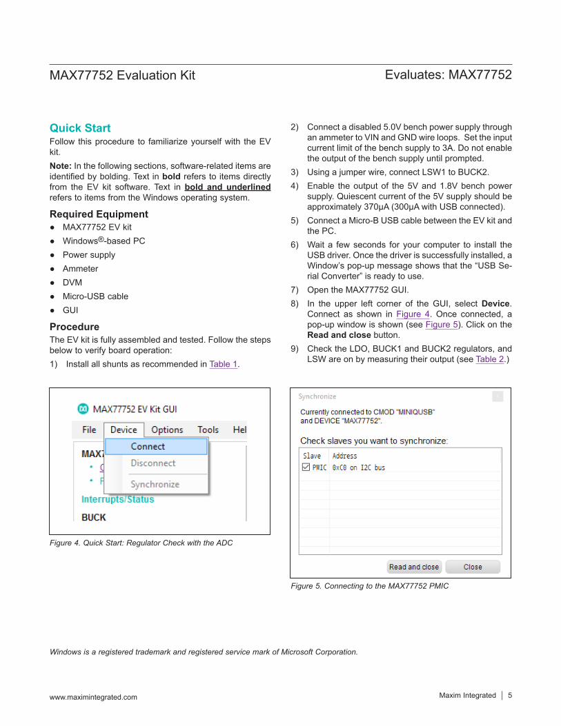
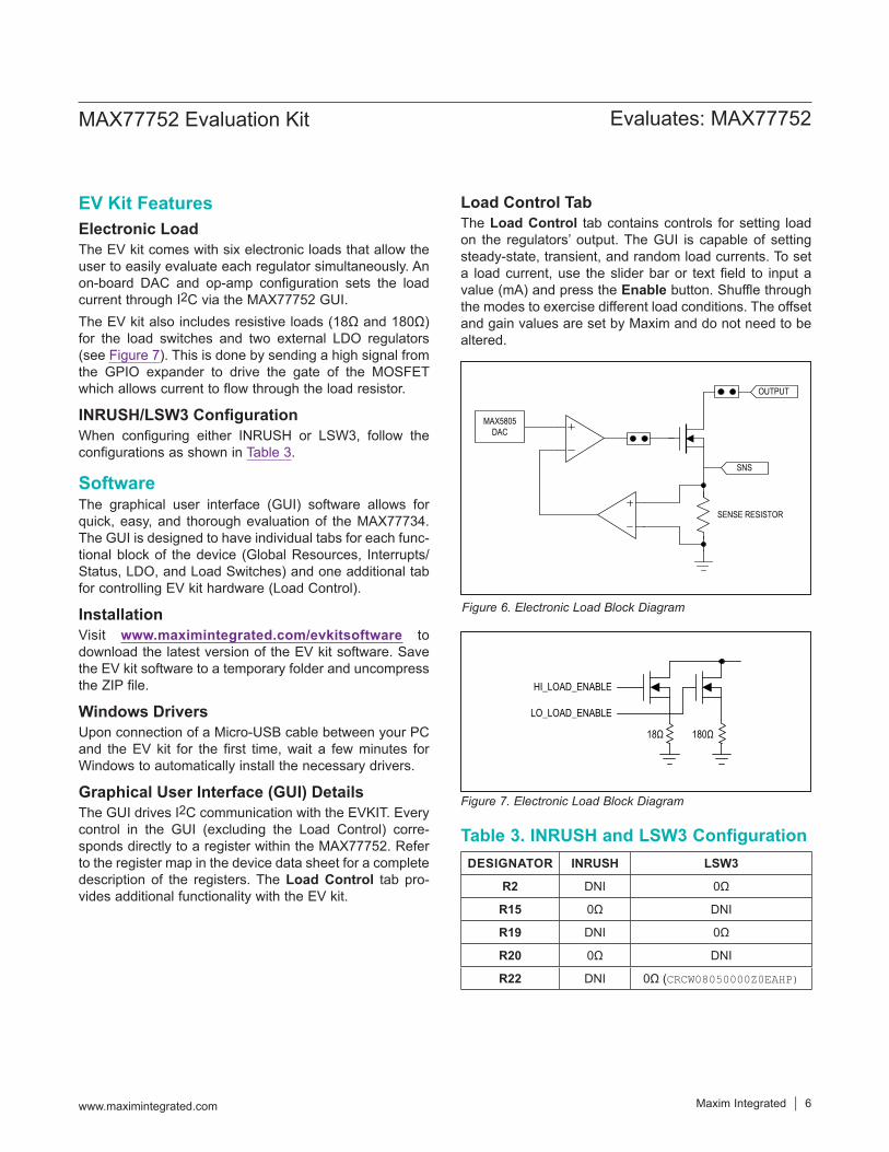
7) Open the MAX77752 GUI.8) In the upper left corner of the GUI, select Device.
Connect as shown in Figure 4. Once connected, a pop-up window is shown (see Figure 5). Click on the Read and close button.
9) Check the LDO, BUCK1 and BUCK2 regulators, and LSW are on by measuring their output (see Table 2.)
Windows is a registered trademark and registered service mark of Microsoft Corporation.
Figure 4. Quick Start: Regulator Check with the ADC
Figure 5. Connecting to the MAX77752 PMIC
Maxim Integrated │ 6www.maximintegrated.com
Evaluates: MAX77752MAX77752 Evaluation Kit
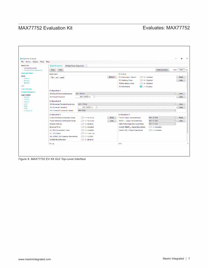
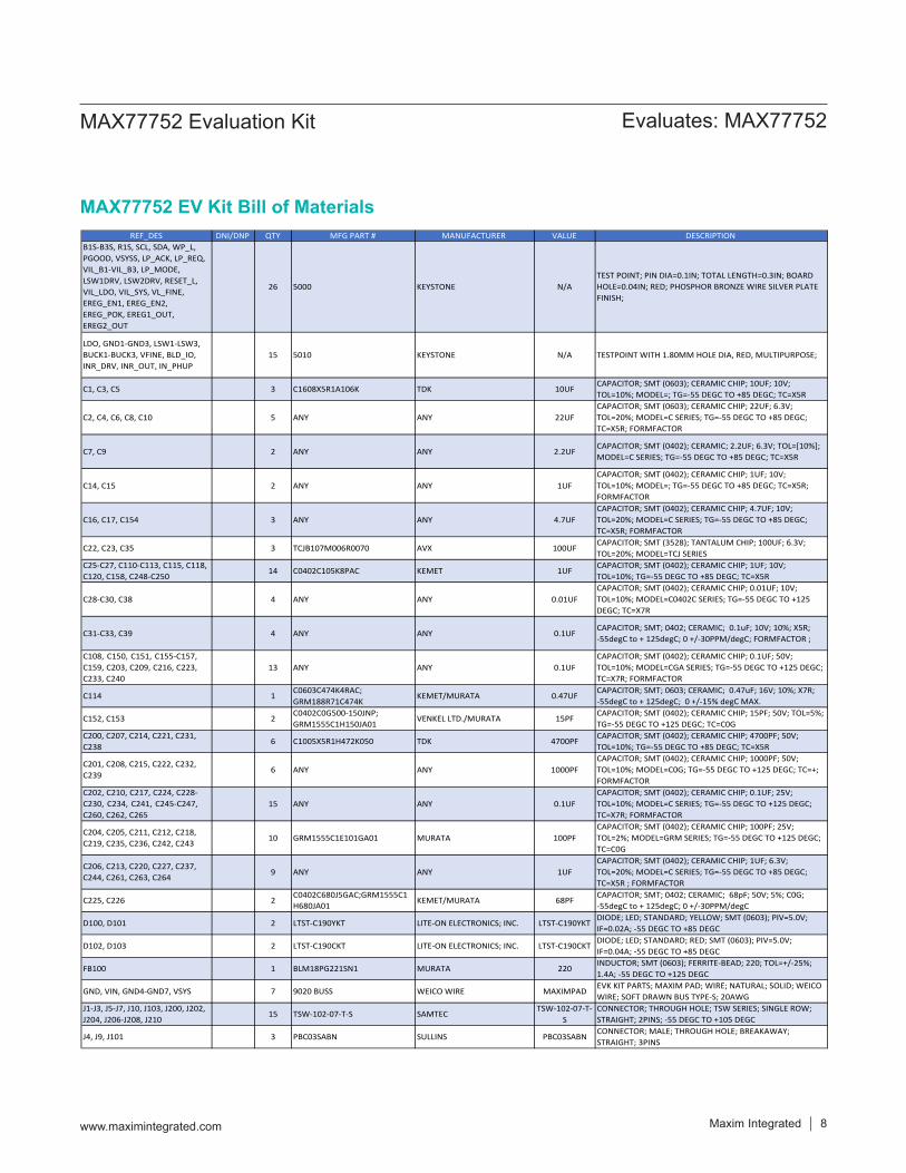
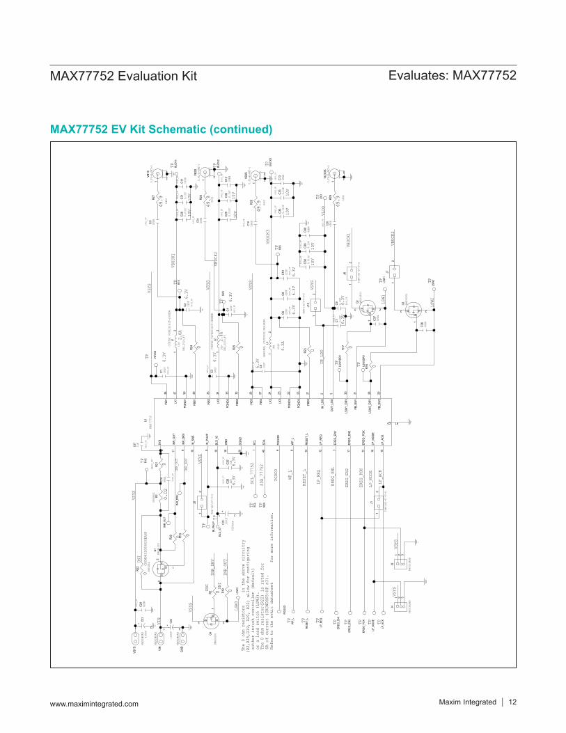
EV Kit FeaturesElectronic LoadThe EV kit comes with six electronic loads that allow the user to easily evaluate each regulator simultaneously. An on-board DAC and op-amp configuration sets the load current through I2C via the MAX77752 GUI.The EV kit also includes resistive loads (18Ω and 180Ω) for the load switches and two external LDO regulators (see Figure 7). This is done by sending a high signal from the GPIO expander to drive the gate of the MOSFET which allows current to flow through the load resistor.
INRUSH/LSW3 ConfigurationWhen configuring either INRUSH or LSW3, follow the configurations as shown in Table 3.
SoftwareThe graphical user interface (GUI) software allows for quick, easy, and thorough evaluation of the MAX77734. The GUI is designed to have individual tabs for each func-tional block of the device (Global Resources, Interrupts/Status, LDO, and Load Switches) and one additional tab for controlling EV kit hardware (Load Control).
InstallationVisit www.maximintegrated.com/evkitsoftware to download the latest version of the EV kit software. Save the EV kit software to a temporary folder and uncompress the ZIP file.
Windows DriversUpon connection of a Micro-USB cable between your PC and the EV kit for the first time, wait a few minutes for Windows to automatically install the necessary drivers.
Graphical User Interface (GUI) DetailsThe GUI drives I2C communication with the EVKIT. Every control in the GUI (excluding the Load Control) corre-sponds directly to a register within the MAX77752. Refer to the register map in the device data sheet for a complete description of the registers. The Load Control tab pro-vides additional functionality with the EV kit.
Load Control TabThe Load Control tab contains controls for setting load on the regulators’ output. The GUI is capable of setting steady-state, transient, and random load currents. To set a load current, use the slider bar or text field to input a value (mA) and press the Enable button. Shuffle through the modes to exercise different load conditions. The offset and gain values are set by Maxim and do not need to be altered.
Table 3. INRUSH and LSW3 Configuration
Figure 6. Electronic Load Block Diagram
Figure 7. Electronic Load Block Diagram
OUTPUT
MAX5805 DAC
SNS
SENSE RESISTOR
HI_LOAD_ENABLE
LO_LOAD_ENABLE
18Ω 180Ω
DESIGNATOR INRUSH LSW3
R2 DNI 0Ω
R15 0Ω DNI
R19 DNI 0Ω
R20 0Ω DNI
R22 DNI 0Ω (CRCW08050000Z0EAHP)
Maxim Integrated │ 7www.maximintegrated.com
Evaluates: MAX77752MAX77752 Evaluation Kit
Figure 8. MAX77752 EV Kit GUI Top-Level Interface
Maxim Integrated │ 8www.maximintegrated.com
Evaluates: MAX77752MAX77752 Evaluation Kit
MAX77752 EV Kit Bill of MaterialsREF_DES DNI/DNP QTY MFG PART # MANUFACTURER VALUE DESCRIPTION
B1S-B3S, R1S, SCL, SDA, WP_L, PGOOD, VSYSS, LP_ACK, LP_REQ, VIL_B1-VIL_B3, LP_MODE, LSW1DRV, LSW2DRV, RESET_L, VIL_LDO, VIL_SYS, VL_FINE, EREG_EN1, EREG_EN2, EREG_POK, EREG1_OUT, EREG2_OUT
26 5000 KEYSTONE N/ATEST POINT; PIN DIA=0.1IN; TOTAL LENGTH=0.3IN; BOARD HOLE=0.04IN; RED; PHOSPHOR BRONZE WIRE SILVER PLATE FINISH;
LDO, GND1-GND3, LSW1-LSW3, BUCK1-BUCK3, VFINE, BLD_IO, INR_DRV, INR_OUT, IN_PHUP
15 5010 KEYSTONE N/A TESTPOINT WITH 1.80MM HOLE DIA, RED, MULTIPURPOSE;
C1, C3, C5 3 C1608X5R1A106K TDK 10UFCAPACITOR; SMT (0603); CERAMIC CHIP; 10UF; 10V; TOL=10%; MODEL=; TG=-55 DEGC TO +85 DEGC; TC=X5R
C2, C4, C6, C8, C10 5 ANY ANY 22UFCAPACITOR; SMT (0603); CERAMIC CHIP; 22UF; 6.3V; TOL=20%; MODEL=C SERIES; TG=-55 DEGC TO +85 DEGC; TC=X5R; FORMFACTOR
C7, C9 2 ANY ANY 2.2UFCAPACITOR; SMT (0402); CERAMIC; 2.2UF; 6.3V; TOL=[10%]; MODEL=C SERIES; TG=-55 DEGC TO +85 DEGC; TC=X5R
C14, C15 2 ANY ANY 1UFCAPACITOR; SMT (0402); CERAMIC CHIP; 1UF; 10V; TOL=10%; MODEL=; TG=-55 DEGC TO +85 DEGC; TC=X5R; FORMFACTOR
C16, C17, C154 3 ANY ANY 4.7UFCAPACITOR; SMT (0402); CERAMIC CHIP; 4.7UF; 10V; TOL=20%; MODEL=C SERIES; TG=-55 DEGC TO +85 DEGC; TC=X5R; FORMFACTOR
C22, C23, C35 3 TCJB107M006R0070 AVX 100UFCAPACITOR; SMT (3528); TANTALUM CHIP; 100UF; 6.3V; TOL=20%; MODEL=TCJ SERIES
C25-C27, C110-C113, C115, C118, C120, C158, C248-C250
14 C0402C105K8PAC KEMET 1UFCAPACITOR; SMT (0402); CERAMIC CHIP; 1UF; 10V; TOL=10%; TG=-55 DEGC TO +85 DEGC; TC=X5R
C28-C30, C38 4 ANY ANY 0.01UFCAPACITOR; SMT (0402); CERAMIC CHIP; 0.01UF; 10V; TOL=10%; MODEL=C0402C SERIES; TG=-55 DEGC TO +125 DEGC; TC=X7R
C31-C33, C39 4 ANY ANY 0.1UFCAPACITOR; SMT; 0402; CERAMIC; 0.1uF; 10V; 10%; X5R; -55degC to + 125degC; 0 +/-30PPM/degC; FORMFACTOR ;
C108, C150, C151, C155-C157, C159, C203, C209, C216, C223, C233, C240
13 ANY ANY 0.1UFCAPACITOR; SMT (0402); CERAMIC CHIP; 0.1UF; 50V; TOL=10%; MODEL=CGA SERIES; TG=-55 DEGC TO +125 DEGC; TC=X7R; FORMFACTOR
C114 1C0603C474K4RAC; GRM188R71C474K
KEMET/MURATA 0.47UFCAPACITOR; SMT; 0603; CERAMIC; 0.47uF; 16V; 10%; X7R; -55degC to + 125degC; 0 +/-15% degC MAX.
C152, C153 2C0402C0G500-150JNP; GRM1555C1H150JA01
VENKEL LTD./MURATA 15PFCAPACITOR; SMT (0402); CERAMIC CHIP; 15PF; 50V; TOL=5%; TG=-55 DEGC TO +125 DEGC; TC=C0G
C200, C207, C214, C221, C231, C238
6 C1005X5R1H472K050 TDK 4700PFCAPACITOR; SMT (0402); CERAMIC CHIP; 4700PF; 50V; TOL=10%; TG=-55 DEGC TO +85 DEGC; TC=X5R
C201, C208, C215, C222, C232, C239
6 ANY ANY 1000PFCAPACITOR; SMT (0402); CERAMIC CHIP; 1000PF; 50V; TOL=10%; MODEL=C0G; TG=-55 DEGC TO +125 DEGC; TC=+; FORMFACTOR
C202, C210, C217, C224, C228-C230, C234, C241, C245-C247, C260, C262, C265
15 ANY ANY 0.1UFCAPACITOR; SMT (0402); CERAMIC CHIP; 0.1UF; 25V; TOL=10%; MODEL=C SERIES; TG=-55 DEGC TO +125 DEGC; TC=X7R; FORMFACTOR
C204, C205, C211, C212, C218, C219, C235, C236, C242, C243
10 GRM1555C1E101GA01 MURATA 100PFCAPACITOR; SMT (0402); CERAMIC CHIP; 100PF; 25V; TOL=2%; MODEL=GRM SERIES; TG=-55 DEGC TO +125 DEGC; TC=C0G
C206, C213, C220, C227, C237, C244, C261, C263, C264
9 ANY ANY 1UFCAPACITOR; SMT (0402); CERAMIC CHIP; 1UF; 6.3V; TOL=20%; MODEL=C SERIES; TG=-55 DEGC TO +85 DEGC; TC=X5R ; FORMFACTOR
C225, C226 2C0402C680J5GAC;GRM1555C1 H680JA01 KEMET/MURATA 68PF
CAPACITOR; SMT; 0402; CERAMIC; 68pF; 50V; 5%; C0G; -55degC to + 125degC; 0 +/-30PPM/degC
D100, D101 2 LTST-C190YKT LITE-ON ELECTRONICS; INC. LTST-C190YKTDIODE; LED; STANDARD; YELLOW; SMT (0603); PIV=5.0V; IF=0.02A; -55 DEGC TO +85 DEGC
D102, D103 2 LTST-C190CKT LITE-ON ELECTRONICS; INC. LTST-C190CKTDIODE; LED; STANDARD; RED; SMT (0603); PIV=5.0V; IF=0.04A; -55 DEGC TO +85 DEGC
FB100 1 BLM18PG221SN1 MURATA 220INDUCTOR; SMT (0603); FERRITE-BEAD; 220; TOL=+/-25%; 1.4A; -55 DEGC TO +125 DEGC
GND, VIN, GND4-GND7, VSYS 7 9020 BUSS WEICO WIRE MAXIMPADEVK KIT PARTS; MAXIM PAD; WIRE; NATURAL; SOLID; WEICO WIRE; SOFT DRAWN BUS TYPE-S; 20AWG
J1-J3, J5-J7, J10, J103, J200, J202, J204, J206-J208, J210
15 TSW-102-07-T-S SAMTECTSW-102-07-T-
SCONNECTOR; THROUGH HOLE; TSW SERIES; SINGLE ROW; STRAIGHT; 2PINS; -55 DEGC TO +105 DEGC
J4, J9, J101 3 PBC03SABN SULLINS PBC03SABNCONNECTOR; MALE; THROUGH HOLE; BREAKAWAY; STRAIGHT; 3PINS
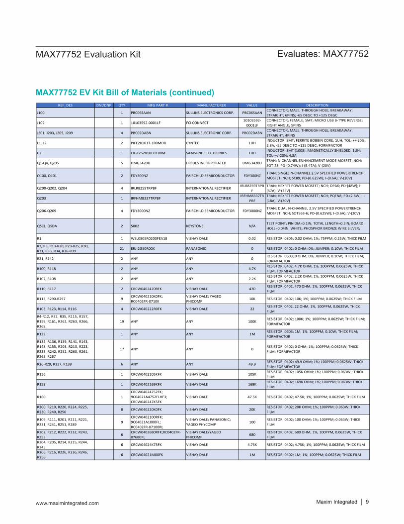
Maxim Integrated │ 9www.maximintegrated.com
Evaluates: MAX77752MAX77752 Evaluation Kit
MAX77752 EV Kit Bill of Materials (continued)REF_DES DNI/DNP QTY MFG PART # MANUFACTURER VALUE DESCRIPTION
J100 1 PBC06SAAN SULLINS ELECTRONICS CORP. PBC06SAANCONNECTOR; MALE; THROUGH HOLE; BREAKAWAY; STRAIGHT; 6PINS; -65 DEGC TO +125 DEGC
J102 1 10103592-0001LF FCI CONNECT10103592-
0001LFCONNECTOR; FEMALE; SMT; MICRO USB B-TYPE REVERSE; RIGHT ANGLE; 5PINS
J201, J203, J205, J209 4 PBC02DABN SULLINS ELECTRONIC CORP. PBC02DABNCONNECTOR; MALE; THROUGH HOLE; BREAKAWAY; STRAIGHT; 4PINS
L1, L2 2 PIFE20161T-1R0MDR CYNTEC 1UHINDUCTOR; SMT; FERRITE BOBBIN CORE; 1UH; TOL=+/-20%; 2.8A; -55 DEGC TO +125 DEGC; FORMFACTOR
L3 1 CIGT252010EH1R0M SAMSUNG ELECTRONICS 1UHINDUCTOR; SMT (1008); MAGNETICALLY SHIELDED; 1UH; TOL=+/-20%; 4.3A
Q1-Q4, Q205 5 DMG3420U DIODES INCORPORATED DMG3420UTRAN; N-CHANNEL ENHANCEMENT MODE MOSFET; NCH; SOT-23; PD-(0.74W); I-(5.47A); V-(20V)
Q100, Q101 2 FDY300NZ FAIRCHILD SEMICONDUCTOR FDY300NZTRAN; SINGLE N-CHANNEL 2.5V SPECIFIED POWERTRENCH MOSFET; NCH; SC89; PD-(0.625W); I-(0.6A); V-(20V)
Q200-Q202, Q204 4 IRLR8259TRPBF INTERNATIONAL RECTIFIERIRLR8259TRPB
FTRAN; HEXFET POWER MOSFET; NCH; DPAK; PD-(48W); I-(57A); V-(25V)
Q203 1 IRFHM8337TRPBF INTERNATIONAL RECTIFIERIRFHM8337TR
PBFTRAN; HEXFET POWER MOSFET; NCH; PQFN8; PD-(2.8W); I-(18A); V-(30V)
Q206-Q209 4 FDY3000NZ FAIRCHILD SEMICONDUCTOR FDY3000NZTRAN; DUAL N-CHANNEL 2.5V SPECIFIED POWERTRENCH MOSFET; NCH; SOT563-6; PD-(0.625W); I-(0.6A); V-(20V)
QSCL, QSDA 2 5002 KEYSTONE N/ATEST POINT; PIN DIA=0.1IN; TOTAL LENGTH=0.3IN; BOARD HOLE=0.04IN; WHITE; PHOSPHOR BRONZE WIRE SILVER;
R1 1 WSL0805R0200FEA18 VISHAY DALE 0.02 RESISTOR; 0805; 0.02 OHM; 1%; 75PPM; 0.25W; THICK FILM
R2, R3, R13-R20, R23-R25, R30, R31, R33, R34, R36-R39
21 ERJ-2GE0R00X PANASONIC 0 RESISTOR; 0402; 0 OHM; 0%; JUMPER; 0.10W; THICK FILM
R21, R142 2 ANY ANY 0RESISTOR; 0603; 0 OHM; 0%; JUMPER; 0.10W; THICK FILM; FORMFACTOR
R100, R118 2 ANY ANY 4.7KRESISTOR, 0402, 4.7K OHM, 1%, 100PPM, 0.0625W, THICK FILM; FORMFACTOR
R107, R108 2 ANY ANY 2.2KRESISTOR, 0402, 2.2K OHM, 1%, 100PPM, 0.0625W, THICK FILM; FORMFACTOR
R110, R117 2 CRCW0402470RFK VISHAY DALE 470RESISTOR, 0402, 470 OHM, 1%, 100PPM, 0.0625W, THICK FILM
R113, R290-R297 9CRCW040210K0FK; RC0402FR-0710K
VISHAY DALE; YAGEO PHICOMP
10K RESISTOR; 0402; 10K; 1%; 100PPM; 0.0625W; THICK FILM
R103, R123, R114, R116 4 CRCW040222R0FK VISHAY DALE 22RESISTOR, 0402, 22 OHM, 1%, 100PPM, 0.0625W, THICK FILM
R4-R12, R32, R35, R115, R157, R159, R161, R262, R263, R266, R268
19 ANY ANY 100KRESISTOR; 0402; 100K; 1%; 100PPM; 0.0625W; THICK FILM; FORMFACTOR
R122 1 ANY ANY 1MRESISTOR; 0603; 1M; 1%; 100PPM; 0.10W; THICK FILM; FORMFACTOR
R135, R136, R139, R141, R143, R148, R155, R203, R213, R223, R233, R242, R252, R260, R261, R265, R267
17 ANY ANY 0RESISTOR; 0402; 0 OHM; 1%; 100PPM; 0.0625W; THICK FILM; FORMFACTOR
R26-R29, R137, R138 6 ANY ANY 49.9RESISTOR; 0402; 49.9 OHM; 1%; 100PPM; 0.0625W; THICK FILM; FORMFACTOR
R156 1 CRCW0402105KFK VISHAY DALE 105KRESISTOR; 0402; 105K OHM; 1%; 100PPM; 0.063W ; THICK FILM
R158 1 CRCW0402169KFK VISHAY DALE 169KRESISTOR; 0402; 169K OHM; 1%; 100PPM; 0.063W; THICK FILM
R160 1CRCW04024752FK; 9C04021A4752FLHF3; CRCW040247K5FK
VISHAY DALE 47.5K RESISTOR; 0402; 47.5K; 1%; 100PPM; 0.0625W; THICK FILM
R200, R210, R220, R224, R225, R230, R240, R250
8 CRCW040220K0FK VISHAY DALE 20KRESISTOR; 0402; 20K OHM; 1%; 100PPM; 0.063W; THICK FILM
R109, R111, R201, R211, R221, R231, R241, R251, R289
9CRCW0402100RFK; 9C04021A1000FL; RC0402FR-07100RL
VISHAY DALE; PANASONIC; YAGEO PHYCOMP
100RESISTOR; 0402; 100 OHM; 1%; 100PPM; 0.063W; THICK FILM
R202, R212, R222, R232, R243, R253
6CRCW0402680RFK;RC0402FR-07680RL
VISHAY DALE/YAGEO PHICOMP
680RESISTOR, 0402, 680 OHM, 1%, 100PPM, 0.0625W, THICK FILM
R204, R205, R214, R215, R244, R245
6 CRCW04024K75FK VISHAY DALE 4.75K RESISTOR; 0402; 4.75K; 1%; 100PPM; 0.0625W; THICK FILM
R206, R216, R226, R236, R246, R256
6 CRCW04021M00FK VISHAY DALE 1M RESISTOR; 0402; 1M; 1%; 100PPM; 0.0625W; THICK FILM
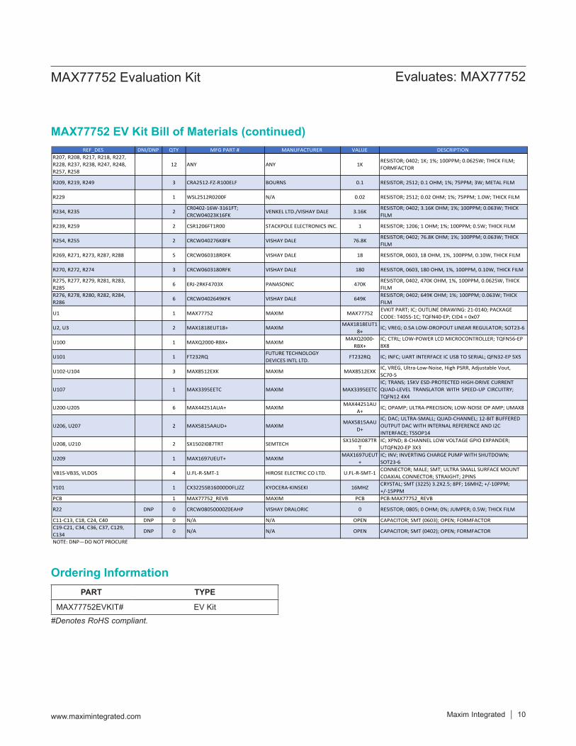
Maxim Integrated │ 10www.maximintegrated.com
Evaluates: MAX77752MAX77752 Evaluation Kit
#Denotes RoHS compliant.
MAX77752 EV Kit Bill of Materials (continued)
Ordering Information
REF_DES DNI/DNP QTY MFG PART # MANUFACTURER VALUE DESCRIPTIONR207, R208, R217, R218, R227, R228, R237, R238, R247, R248, R257, R258
12 ANY ANY 1KRESISTOR; 0402; 1K; 1%; 100PPM; 0.0625W; THICK FILM; FORMFACTOR
R209, R219, R249 3 CRA2512-FZ-R100ELF BOURNS 0.1 RESISTOR; 2512; 0.1 OHM; 1%; 75PPM; 3W; METAL FILM
R229 1 WSL2512R0200F N/A 0.02 RESISTOR; 2512; 0.02 OHM; 1%; 75PPM; 1.0W; THICK FILM
R234, R235 2CR0402-16W-3161FT; CRCW04023K16FK
VENKEL LTD./VISHAY DALE 3.16KRESISTOR; 0402; 3.16K OHM; 1%; 100PPM; 0.063W; THICK FILM
R239, R259 2 CSR1206FT1R00 STACKPOLE ELECTRONICS INC. 1 RESISTOR; 1206; 1 OHM; 1%; 100PPM; 0.5W; THICK FILM
R254, R255 2 CRCW040276K8FK VISHAY DALE 76.8KRESISTOR; 0402; 76.8K OHM; 1%; 100PPM; 0.063W; THICK FILM
R269, R271, R273, R287, R288 5 CRCW060318R0FK VISHAY DALE 18 RESISTOR, 0603, 18 OHM, 1%, 100PPM, 0.10W, THICK FILM
R270, R272, R274 3 CRCW0603180RFK VISHAY DALE 180 RESISTOR, 0603, 180 OHM, 1%, 100PPM, 0.10W, THICK FILM
R275, R277, R279, R281, R283, R285
6 ERJ-2RKF4703X PANASONIC 470KRESISTOR, 0402, 470K OHM, 1%, 100PPM, 0.0625W, THICK FILM
R276, R278, R280, R282, R284, R286
6 CRCW0402649KFK VISHAY DALE 649KRESISTOR; 0402; 649K OHM; 1%; 100PPM; 0.063W; THICK FILM
U1 1 MAX77752 MAXIM MAX77752EVKIT PART; IC; OUTLINE DRAWING: 21-0140; PACKAGE CODE: T4055-1C; TQFN40-EP; CID4 = 0x07
U2, U3 2 MAX1818EUT18+ MAXIMMAX1818EUT1
8+IC; VREG; 0.5A LOW-DROPOUT LINEAR REGULATOR; SOT23-6
U100 1 MAXQ2000-RBX+ MAXIMMAXQ2000-
RBX+IC; CTRL; LOW-POWER LCD MICROCONTROLLER; TQFN56-EP 8X8
U101 1 FT232RQFUTURE TECHNOLOGY DEVICES INTL LTD.
FT232RQ IC; INFC; UART INTERFACE IC USB TO SERIAL; QFN32-EP 5X5
U102-U104 3 MAX8512EXK MAXIM MAX8512EXKIC, VREG, Ultra-Low-Noise, High PSRR, Adjustable Vout, SC70-5
U107 1 MAX3395EETC MAXIM MAX3395EETCIC; TRANS; 15KV ESD-PROTECTED HIGH-DRIVE CURRENT QUAD-LEVEL TRANSLATOR WITH SPEED-UP CIRCUITRY; TQFN12 4X4
U200-U205 6 MAX44251AUA+ MAXIMMAX44251AU
A+IC; OPAMP; ULTRA-PRECISION; LOW-NOISE OP AMP; UMAX8
U206, U207 2 MAX5815AAUD+ MAXIMMAX5815AAU
D+
IC; DAC; ULTRA-SMALL; QUAD-CHANNEL; 12-BIT BUFFERED OUTPUT DAC WITH INTERNAL REFERENCE AND I2C INTERFACE; TSSOP14
U208, U210 2 SX1502I087TRT SEMTECHSX1502I087TR
TIC; XPND; 8-CHANNEL LOW VOLTAGE GPIO EXPANDER; UTQFN20-EP 3X3
U209 1 MAX1697UEUT+ MAXIMMAX1697UEUT
+IC; INV; INVERTING CHARGE PUMP WITH SHUTDOWN; SOT23-6
VB1S-VB3S, VLDOS 4 U.FL-R-SMT-1 HIROSE ELECTRIC CO LTD. U.FL-R-SMT-1CONNECTOR; MALE; SMT; ULTRA SMALL SURFACE MOUNT COAXIAL CONNECTOR; STRAIGHT; 2PINS
Y101 1 CX3225SB16000D0FLJZZ KYOCERA-KINSEKI 16MHZCRYSTAL; SMT (3225) 3.2X2.5; 8PF; 16MHZ; +/-10PPM; +/-15PPM
PCB 1 MAX77752_REVB MAXIM PCB PCB:MAX77752_REVB
R22 DNP 0 CRCW08050000Z0EAHP VISHAY DRALORIC 0 RESISTOR; 0805; 0 OHM; 0%; JUMPER; 0.5W; THICK FILM
C11-C13, C18, C24, C40 DNP 0 N/A N/A OPEN CAPACITOR; SMT (0603); OPEN; FORMFACTORC19-C21, C34, C36, C37, C129, C134
DNP 0 N/A N/A OPEN CAPACITOR; SMT (0402); OPEN; FORMFACTOR
NOTE: DNP—DO NOT PROCURE
PART TYPE
MAX77752EVKIT# EV Kit
Maxim Integrated │ 11www.maximintegrated.com
Evaluates: MAX77752MAX77752 Evaluation Kit
0b0100 00110x43
0b0100 00100x42
0b010 00010x21
ADDR=3.3V
0b0100 00010x41
0b0100 00000x40
0b010 00000x20ADDR=GND
SX1502 U208
GPIO EXPANDER
GPIO EXPANDER
SX1502 U210
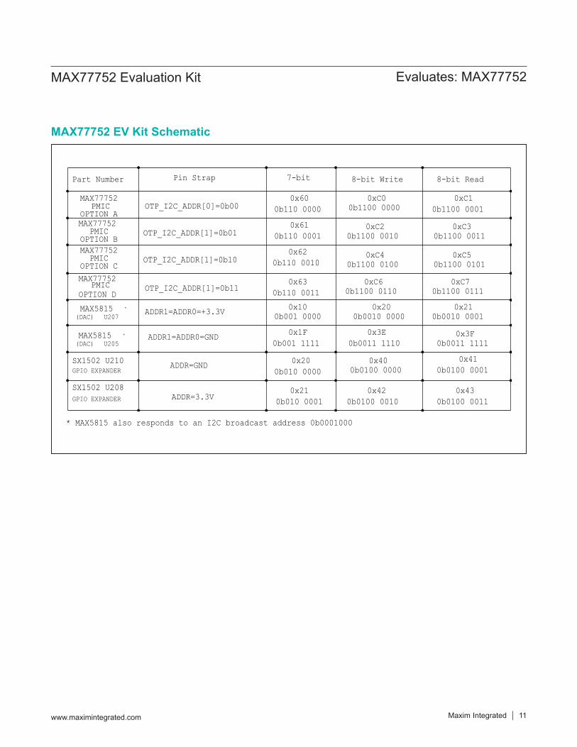
* MAX5815 also responds to an I2C broadcast address 0b0001000
Part Number 8-bit Write 8-bit Read
0b1100 00010xC1
7-bit
0b0011 11110x3F0x3E
0b0011 11100b001 11110x1F
ADDR1=ADDR0=+3.3V
ADDR1=ADDR0=GNDU205(DAC)
0b001 0000 0b0010 0000 0b0010 00010x10 0x210x20
0x600b110 0000 0b1100 0000
0xC0
0x61 0xC20b110 0001 0b1100 0010 0b1100 0011
0xC3
0x620b110 0010 0b1100 0101
0x63
0b1100 0100
0b1100 0110 0b1100 01110b110 0011
Pin Strap
MAX77752PMIC
OPTION AOTP_I2C_ADDR[0]=0b00
MAX77752PMIC
OPTION BMAX77752
PMICOPTION C
MAX77752PMIC
OPTION D
OTP_I2C_ADDR[1]=0b10
OTP_I2C_ADDR[1]=0b01
OTP_I2C_ADDR[1]=0b11
0xC4 0xC5
0xC6 0xC7
MAX5815
MAX5815U207(DAC)
*
*
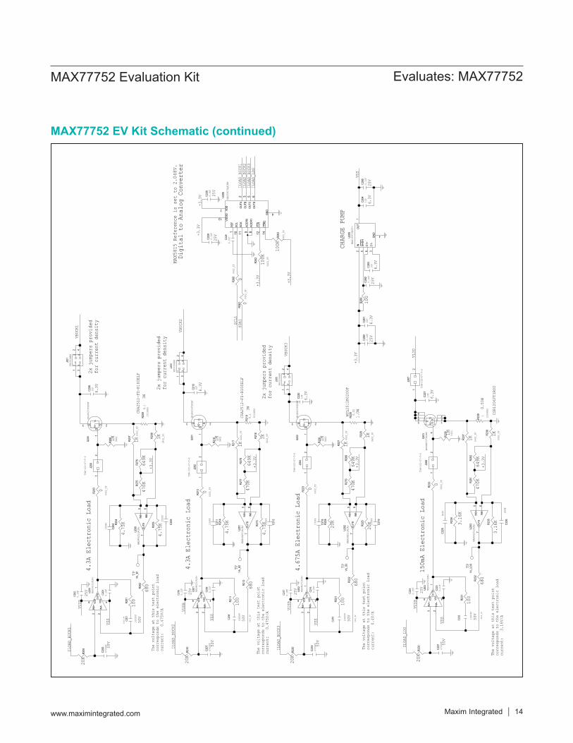
MAX77752 EV Kit Schematic
Maxim Integrated │ 12www.maximintegrated.com
Evaluates: MAX77752MAX77752 Evaluation Kit
SAMSUNG, CIGT252010EH1R0M
CYNTEC PIFE20161T-1R0MDR
CYNTEC PIFE20161T-1R0MDR
4.3A
2.8A
2.8A
in the above circuitry
for more information.
(R2,R15,R19, R20, R22) allow for configuring
The 0 ohm resistor(R22) is rated for
Refer to the evkit datasheet
or a load switch (LSW3).
6A of current (CRCW0805-HP e3).
either inrush controller (default)
The 0 ohm resistors
321J9
321J4
INR_
OUT
R19
R2
2
1
3
Q4
R20
21
J1
C38
C39
C40
C36
C37
R1S
21
C35
C20
C19C3
4
C21
1
3
2VLDO
S
R29
R26R2
8
R27
1
3
2VB3S
1
3
2VB2S
1
3
2VB1S
21
J5
C18
LSW
3
VSYS
S
C30
C29
C28
C33
C32
C31
LSW
2DRV
LSW
1DRV
R16
R17
INR_
DRV
R15
21
J10
21
J6
21
J7
B3S
B2S
B1S
21
C22
21
C23
C24
R21
R22
R24
R25
R23
C25
C26
C27
GNDVI
N2
1
3Q
1
VSYS
C13
C12
C11
LP_A
CK
LP_M
ODE
EREG
_PO
K
EREG
_EN2
EREG
_EN1
LP_R
EQ
RESE
T_L
WP_
L
PGO
OD
SDA
SCL
BLD_
IOIN_P
HUP
R1
LDO
BUCK
3
BUCK
2
BUCK
1
LSW
1
LSW
2
2
1
3
Q3
2
1
3
Q2
C9C7
C10
C8C6
21
L3
21
L1
C4
C2
C5
C3C1
21
L2
4 5 19 8401 136
23223536 325243437 2830
12 16 1511 9
27263338
10
2
18
2931213239
14177
41
20
U1
INR_OUT
0DNI
0INR_DRV
DNI
DMG3
420U
00
0
0
0
0 0
TPLP_REQ
VSYS
0805
RES
DNI
TP
0603
_FF
0OP
EN
0805
RES
DMG3
420U
CRCW08050000Z0EAHP
VLDO
VSYS
TSW-
102-
07-T
-S
OPEN
OPEN
0603_FF
10V
0402_FF
0.01
UF
0.01
UF
0402_FF
10V
10V
0402_FF
0.1U
F
0402_FF
10V
OPEN
OPEN
49.9
49.949.9
49.9
U.FL
-R-S
MT-1
OPEN
U.FL
-R-S
MT-1
OPENOP
ENU.
FL-R
-SMT
-1
OPEN
0.1U
F0.
01UF
0603_FF
0402_FF
10V
0402_FF
10V
0603_FF
OPEN
10V
0402_FF
0.1U
F
VBUCK1
0402_FF
0.01
UF
OPEN
TP
0603_FF
10UF
6.3V
2520
TP
DMG3
420U
DMG3
420U
0402_FF
6.3V
0402_FF
6.3V
2.2U
F2.
2UF
IND_
2016
_FF
IND_
2016
_FF
1UH
1UH
TP
22UF
0603_FF6.
3V
TP
0603_FF
6.3V
22UF
6.3V
10UF
0603_FF
VSYS
6.3V
22UF
0603_FF
22UF
0603_FF
6.3V
22UF
0603_FF
6.3V
VBUCK2
VBUCK1
TSW-
102-
07-T
-S
LSW1
TPTPTP
LSW2
0603_FF
6.3V
10UF
VSYS
VBUCK3
TP
0402_FF
0402
0402_FF
0402_FF
0402
0402_FF
0402
TP
1UF
0402_FF
1UF
1UF
0402_FF
6.3V
6.3V
100U
F
TPTPTP
TP
MAX77752
IN_LDO
SDA_77752
VSYS
TP
WP_L
0.1U
F
0402
VBUCK2
TPU.
FL-R
-SMT
-1
10V
LP_ACK
TPTP
EREG_EN1
RESET_L
SCL_77752
1UH
0402_FF
TSW-
102-
07-T
-S0.02
0603_FF
INR_OUT
TP
PGOOD
TP
TP
INR_DRV
LP_MODE
MAXIMPAD
100U
F
0603_FF
0
TP TP
VSYS
PBC0
3SAB
NPB
C03S
ABN
LSW3OPEN
VSYS
3528
CAP
EREG_EN2
EREG_POK
TSW-
102-
07-T
-S
MAXIMPAD
100U
F
MAXIMPAD
VSYS
VIN
TP
VSYS
GS
D
GSD
GSD
GSD
+
++
EP
SDA
FBB1
INB1 LX
1
PGND
1
PGND
2
LX2
INB2
FBB2
FBLS
W1
LSW
1_DR
V
FBLS
W2
LSW
2_DR
V
INB3
INB3 LX
3
LX3
PGND
3
PGND
3
FBB3
DGND
BLD_
IO
GND
EREG
_EN2
EREG
_EN1
WP_
L
EREG
_PO
K
RESE
T_L
LP_R
EQ
INR_
OUT
IN_S
NS
INR_
DRV
LP_M
ODE
LP_A
CK
PGO
OD
IN_P
HUP
SYS
OUT
_LDO
IN_L
DO
SCL
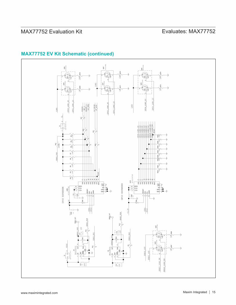
MAX77752 EV Kit Schematic (continued)

Maxim Integrated │ 13www.maximintegrated.com
Evaluates: MAX77752MAX77752 Evaluation Kit
The voltage at this test point
corresponds to the electronic load
25mA Electronic Load
inte
rnal
ref
eren
ce f
or 2
.048
V.So
ftwa
re c
onfi
gure
s th
e MA
X581
5
current: 0.475 V/A
3A Electronic Load
Digital to Analog Converter
The voltage at this test point
corresponds to the electronic load
current: 76.8V/A
2x j
umpe
rs p
rovi
ded
for
curr
ent
dens
ity
TP2
TP1
GND
7
43
21
J209
GND
4
GND
5GND
2
GND
3
GND
1
GND
6
48
123
U205
765
U205
765
U204
48
123
U204
R286
R285
R284
R283
C233
C240
VFIN
E
C238
R250
C239
R251
C241
R253
R255
C243
R254
R252
21
J210
C242
R258
R257
R256
R259
VL_F
INE
2
1
3
Q20
5C2
44
C231
R240
C232
R241
C234
R243
R245
C236
R244
R242
21
J208
C235
R248
R247
R246
2
1
3
Q20
4
R249
VIL_
SYS
C237
R265
R267
R266
R268
13
7
11101
6532
4
89 1412
U207
C246
C245
C247
IRLR
8259
TRPB
F
1M 0402
TSW-
102-
07-T
-S
4700
PF 50V
100
0402
_FF
1206
RES
TP
0402
_FF
100K
4.75K
VSS
MAX4
4251
AUA+
MAXI
MPAD
0402
_FF
1000
PF
VUSB
4.75K
100P
F
76.8K
0402 0402
100P
F
76.8K
MAX4
4251
AUA+
649K
SCL1
SDA1
+3.3V
470K
TP
004
02_F
F
+3.3V
649K
470K
+3.3V
100P
F
TP TP
MAXI
MPAD
MAXI
MPAD
MAX4
4251
AUA+
VUSB
MAX4
4251
AUA+
680
TP
680
FINE
TP
DMG3
420U
ILOAD_FINE
ILOAD_SYS
50V
4700
PF
20K
50V
1000
PF
0.1U
F
25V
20K
50V
0.1U
F
25V
0402
_FF
0402
_FF
0402
_FF
100K
00
+3.3V
ILOAD_FINE
ILOAD_SYS
+3.3V
0.1U
F
25V
0.1U
F25V
0.1U
F
MAX5
815A
AUD+
+3.3V
100
0.1U
F
0.1U
FVSS
0402
_FF
+3.3V
6.3V
1UF
04021M 1K 1K
0402
_FF
1UF
6.3V
0402
_FF
1K
0402
_FF
1K
004
02_F
F
TSW-
102-
07-T
-S
TP TP
MAXI
MPAD
0.1
2512
RES
CRA2512-FZ-R100ELF
1
CSR1206FT1R00
0.50W
3W
100P
F
VSYS
PBC0
2DAB
N 43
21
INA+
OUT
AIN
A-
VDD
VSS
OUT
BIN
B+ INB-
OUT
BIN
B+ INB-
INA+
OUT
AIN
A-
VDD
VSS
GSD
GSD
LDAC
VDDI
O
CLR
ADDR
0AD
DR1
OUT
DO
UTC
OUT
BO
UTA
REF
VDD
SCL
SDA
GND
MAX77752 EV Kit Schematic (continued)
Maxim Integrated │ 14www.maximintegrated.com
Evaluates: MAX77752MAX77752 Evaluation Kit4.
3A E
lect
roni
c Lo
ad
2x j
umpe
rs p
rovi
ded
for
curr
ent
dens
ity
The voltage at this test point
corresponds to the electronic load
2x j
umpe
rs p
rovi
ded
for
curr
ent
dens
ity
4.3A
Ele
ctro
nic
Load
2x j
umpe
rs p
rovi
ded
for
curr
ent
dens
ity
current: 3.16V/A
corresponds to the electronic load
The voltage at this test point
current: 0.475V/A
The voltage at this test point
corresponds to the electronic load
current: 0.475V/A
CHAR
GE P
UMP
Digi
tal
to A
nalo
g Co
nver
ter
MAX5
815
Refe
renc
e is
set
to
2.04
8V.
150m
A El
ectr
onic
Loa
d
4.67
5A E
lect
roni
c Lo
ad
current: 0.4V/A
The voltage at this test point
corresponds to the electronic load
43
21
J205
43
21
J201
43
21
J203
48
123
U203
765
U203
765
U202
48
123
U202
48
123
U201
765
U201
765
U200
48
123
U200
R289
C263
C262
C264
C261
C265
C260
12
4
365
U209
R282
R281
R280
R279
R278
R277
R276
R275
C223
C216
C209
C203
C221
R230
C222
R231
R232
C224
C226
R235R2
34
R233
C225
21
J206
R238
R237
R239
VIL_
LDO
R236
321
4
8765
Q20
3C2
27
21
J207
C214
R220
C215
R221
R222
C217
C219
R225R2
24
R223
C218
21
J204
R228
R227
R229
VIL_
B3
R226
2
1
3
Q20
2C2
20
C207
R210
C208
R211
R212
C210
C212
R215R2
14
R213
C211
21
J202
R218
R217
R219
VIL_
B2
R216
2
1
3
Q20
1C2
13
C200
R261
R260
2
1
3
Q20
0
21
J200
C206
R262
VIL_
B1
R263
13
7
11101
6532
4
89 1412
U206
C228
C229
C230
R200
R209
R203
R208
R207
R206
R204
R205
C204 C2
05
C202
R202
R201
C201
1K
2512
RES
VSS
TSW-
102-
07-T
-S
CRA2512-FZ-R100ELF
1M
1000
PF
+3.3V
649K
3WCRA2512-FZ-R100ELF
0402
_FF
0.02
1.0W
WSL2512R0200F
PBC0
2DAB
N
PBC0
2DAB
N
VBUCK1
3W
3.16
K
68PF 68
PF
3.16
K
20K
4.75
K
4.75
K 100P
F
100P
F
100P
F
100P
F
100P
F
100P
F
0.50W
CSR1206FT1R00
1206
RES
12512
RES
0.1
TP
680
TP
680
TP
680
680
20K
0402
_FF
0402
_FF
0SDA1SCL1
0
100K
0402
_FF
100K
0402
_FF
MAX5
815A
AUD+
0.1U
F
25V
0.1U
F
+3.3V
+3.3V
+3.3V
+3.3V
ILOAD_LDO
ILOAD_BUCK3
ILOAD_BUCK2
ILOAD_BUCK1
20K
1000
PF
50V
25V
4700
PF 50V
20K
25V
0.1U
F
4700
PF 50V
1000
PF
50V
25V
0.1U
F
0.1U
F
0402_FF
1000
PF
50V
0402_FF
0402_FF
VUSB
ILOAD_BUCK1
25V
50V
0402_FF
20K
4700
PF 50V
ILOAD_BUCK2
ILOAD_BUCK3
ILOAD_LDO
50V
4700
PF
VUSB
VUSB
6.3V
1UF
1K
TSW-
102-
07-T
-S
6.3V
1UF
VLDO
1M
0402
_FF
0
0402
_FF
0
04021M
0402
_FF
00.
1UF
0.1U
F
0.1U
F
0.1U
F
VSS
100
100
100
+3.3V
0.1U
F
25V
1UF
100
MAX1
697U
EUT+
1UF
6.3V
0.1U
F
25V
1UF
6.3V
0.1U
F
25V
100
0.1U
F
25V
1UF
6.3V
VSS
MAX4
4251
AUA+
VUSB
VSS
MAX4
4251
AUA+
MAX4
4251
AUA+
MAX4
4251
AUA+
MAX4
4251
AUA+
VBUCK3
VBUCK2
PBC0
2DAB
N
0.1
1K
649K
649K
1K
0402
_FF
1K
0402
0402
_FF
0402
_FF
1K04
02_F
F 1K
IRFH
M833
7TRP
BF 1M 0402
0402
_FF
0402
_FF
1K
+3.3V
TSW-
102-
07-T
-S
+3.3V
0.1U
F
MAX4
4251
AUA+
TP
20K
470K
470K
0402
_FF
0
4.75
K
MAX4
4251
AUA+
470K
0402 0402
_FF
649K
4.75
K
470K
MAX4
4251
AUA+
VSS
TSW-
102-
07-T
-S
+3.3V
6.3V
IRLR
8259
TRPB
F
IRLR
8259
TRPB
F
TSW-
102-
07-T
-SIR
LR82
59TR
PBF
1UF
6.3V
43
21
43
21
43
21
INA+
OUT
AIN
A-
VDD
VSS
OUT
BIN
B+ INB-
OUT
BIN
B+ INB-
INA+
OUT
AIN
A-
VDD
VSS
INA+
OUT
AIN
A-
VDD
VSS
OUT
BIN
B+ INB-
OUT
BIN
B+ INB-
INA+
OUT
AIN
A-
VDD
VSS
OUT
C1-
C1+
GND
IN SHDN
SD
G
GSD
GSD
GSD
LDAC
VDDI
O
CLR
ADDR
0AD
DR1
OUT
DO
UTC
OUT
BO
UTA
REF
VDD
SCL
SDA
GND
MAX77752 EV Kit Schematic (continued)
Maxim Integrated │ 15www.maximintegrated.com
Evaluates: MAX77752MAX77752 Evaluation Kit
GPIO EXPANDER
GPIO EXPANDER
R35
R32
R38
R39
R31
R30
R33
R34
R37
R36
R10
R4R5
R6R7
R8R9
R11
R12
21
J3
C250
C14
R3
5
261
4
3
U2
R18
R14
C16
EREG
2_O
UT
R13
C15
21
J2
C17
EREG
1_O
UT
5
261
4
3
U3
R297
R296
R295
R294
R293
R292
R291
R290
C248
C249
14177
2 41
11
133
2019161510965
188
EP
12
U208
R288
R287
4
5
3
Q20
9
1
2
6
Q20
9
14177
2 41
11
133
2019161510965
188
EP
12
U210
R273
1
2
6
Q20
8
R274
4
5
3
Q20
8
R271
R272
4
5
3
Q20
7
1
2
6
Q20
7
R269
R270
1
2
6
Q20
6
4
5
3
Q20
6
0
10V
0
+3.3V
EREG1_OUT
0LP_ACK
0LP_MODE
0LP_REQ
0RESET_L
0WP_L
0PGOOD
0EREG_EN2
0EREG_EN1
0EREG_POK
10V0
EREG_POK
TSW-
102-
07-T
-S
MAX1
818E
UT18
+
0402_FF
EREG2_LOAD_EN
EREG1_LOAD_EN
GPO5_LSW3_LO
GPO4_LSW3_HI
NINT
GPO3_LSW2_LO
GPO2_LSW2_HI
GPO1_LSW1_LO
GPO0_LSW1_HI
SCL1
SDA1
0402_FF
1UF
10K
10K
10K
10K
10K
10K
10K
10K
VL
TSW-
102-
07-T
-S
0402_FF
100K
100K
100K
EREG2_OUT
FDY3
000N
Z
18
VSYS
1UF
10V
0402_FF
1UF
GPO4_LSW3_HI
LSW3
GPO5_LSW3_LO
1818
0
FDY3
000N
ZFD
Y300
0NZ
GPO2_LSW2_HI
GPO3_LSW2_LO
1818
0
FDY3
000N
ZFD
Y300
0NZ
GPO0_LSW1_HI
LSW1
GPO1_LSW1_LO
FDY3
000N
ZFD
Y300
0NZ
180
18
100K
SX15
02I0
87TR
T
EREG_POK
LSW2
+3.3V
1UF
SX15
02I0
87TR
T
0402_FF
EREG1_OUT
EREG1_LOAD_EN
18
10V
FDY3
000N
Z
EREG2_LOAD_EN
100K
100K
100K
NINT
MAX1
818E
UT18
+
TP
0402_FF
VL10
0K10
0K
1UF
SCL1
100K
TP
4.7U
F
100K
SDA1
0402_FF
4.7U
F
EREG2_OUT
G
D S
SHDN
SET
POK
OUT
IN
GND
SHDN
SET
POK
OUT
IN
GND
G
D S
NC2NC1EP
I/O7
I/O6
GNDVCC2
I/O5
I/O4
VDDM
ADDR
NINTI/O
3I/O
2
GNDVCC1
I/O1
I/O0
SCL
SDA
NRES
ET
G
D S
G
D S
G
D S
NC2NC1EP
I/O7
I/O6
GNDVCC2
I/O5
I/O4
VDDM
ADDR
NINTI/O
3I/O
2
GNDVCC1
I/O1
I/O0
SCL
SDA
NRES
ETG
D S
G
D S
G
D S
MAX77752 EV Kit Schematic (continued)

Maxim Integrated │ 16www.maximintegrated.com
Evaluates: MAX77752MAX77752 Evaluation Kit
3.3V
LDO
2.5V
LDO
MAX3395 I/0VCCx PINS HAVE INTERNAL PULL-UP RESISTORS TO VCC
MAX3395 I/0VLx PINS HAVE INTERNAL 10K PULL-UP RESISTORS TO VL.
1.8V
LDO
21
J103
R114
R113
R117
KA
D103
R116
R160
R161
R159
R158
R157
R156
R110
R143
R115
R122
C120
2
1
3
Q10
1
2
1
3
Q10
0
C134
C129
QSC
L
QSD
A
R136
R135
R139R1
41
R137R1
38R1
07R1
08
474645
22
40
48
201918171615
1413121110987654321
5655545352515049
4443
39 38 37 36 34 33 32 31
27262524
4142 35
23
57
21
30 29
28
U100
C150
PO3
PO7
PO6
PO5
PO4
PO1
PO2
PO0
R148
C151
R155
R100
C152
31
42
Y101
C153
654321
J100
R118
C157
12
11
4321
78910
5
13
6
U107
C115
321J1
01
C113
C118
C158
3
51
2
4
U102
C155
C154
C112
C111
C110
KA D1
00
C114
R142
R109
R111
R103
R123
C156
C159
C108
2 1FB10
0
KA
D102
KA
D101
3
51
2
4
U103
3
51
2
4
U104
11109876
54321
J102
1
19
1415
30 262 32 318 2827
29252313125
20174
33
31 6 78 911102122
24
16
U101
470
0402
0402470LTST
-C19
0CKT
+3.3
V
VUSB
+3.3
V
PBC0
6SAA
N
SCL1
SDA1
+3.3
V
4.7K
50V
15PF
50V
15PF
16MH
Z
00
0
0402
_FF
100K
0402
_FF
0402
_FF
100K
100K
0
0
0
SDA-
LS
VL
+3.3
V+1
.8V
PBC0
3SAB
N
2.2K
2.2K
0
RTSN
DTRNRIN
DCDN
+3.3
V
VUSB
0603
_FF
0
0.1UF
50V
0.1U
F50V
50V
0.1U
F
0.1U
F
50V
0.1U
F
50V
0.1U
F
50V
0.1U
F
50V
0402
_FF
100K
0402_FF
6.3V
1UF
4.7K
47.5K
6.3V
1UF
0402_FF
+2.5
V
0402_FF
1UF
6.3V
0402_FF
1UF
0402_FF
1UF
MAX8
512E
XK
MAX8
512E
XK
TPTP
CTSN
0402_FF 0.47
UF0603_FF10V
0402
_FF100
0402
_FF
100
4.7U
F
10V
0402_FF6.3V
1UF
MAXQP05
+3.3
V TO
+5.
25V
6.3V
6.3V
0402_FF
1UF 6.3V
0603
_FF
1M
1010
3592
-000
1LF
0402_FF
0402_FF
0402
_FF
FDY3
00NZ
OPEN
OPEN
49.9
DSRN
P07P06
MAXQP03P04
P02P01
+3.3
V
TXD
RXD
TPTP
TP
TP
TPTP
TP
TP
MAXQ
2000
-RBX
+
MAX3
395E
ETC
0402
_FF
0402
_FF
2222
LTST
-C19
0YKT
LTST
-C19
0YKT
220
0603
FT23
2RQ
CTSN
DCDN
DSRN
DTRN
RINRTSN
RXD
TXD
169K
105K
0402
0402
0402
MAX8
512E
XKVU
SBVU
SB
+3.3
V
+2.5
V
SCL-
LS
6.3V
0402_FF
1UF
+1.8
V
SDA_
7775
2
SCL_
7775
2
FDY3
00NZ 0402
_FF
49.9
LTST
-C19
0CKT
10K
+3.3
V
NINT
22
22
P00
NINT
TSW-
102-
07-T
-S
VUSB
VIN
EP
GND
VCC
VL
EN
I/OVC
C4
I/OVC
C3
I/OVC
C2
I/OVC
C1
I/OVL
4
I/OVL
3
I/OVL
2
I/OVL
1
INININININO
UT
INO
UT
OUT
SHDN
FBG
ND
INO
UT
SHDN
FBG
ND
IN
OUT
SHDN
FBG
ND
IN
SHIE
LD P
INS
54321
D
GS
D
GS
INININININ
32KO
UTSE
G21
/P3.
5/IN
T5SE
G20
/P3.
4/IN
T4SE
G19
/P2.
7SE
G18
/P2.
6SE
G17
/P2.
5SE
G16
/P2.
4SE
G15
/P1.
7SE
G14
/P1.
6SE
G13
/P1.
5SE
G12
/P1.
4SE
G11
/P1.
3SE
G10
/P1.
2SE
G9/
P1.1
SEG
8/P1
.0
SEG7/P0.7/INT3SEG6/P0.6/INT2SEG5/P0.5/INT1SEG4/P0.4/INT0
SEG3/P0.3SEG2/P0.2SEG1/P0.1SEG0/P0.0
VADJVLCD2VLCD1VLCD
P7.1/RX0/INT15P7.0/TX0/INT14
HFXI
NHF
XOUT
VDD
P6.5
/T0/
WKO
UT1
P6.4
/T0B
/WKO
UT0
P6.1
/T1/
INT1
3P6
.0/T
1B/IN
T12
GND
P5.7
/MIS
OP5
.6/S
CLK
P5.5
/MO
SIP5
.4/S
S
32KI
N
RESETP4.3/TDOP4.2/TMSP4.1/TDI/INT9P4.0/TCK/INT8GNDVDDIOCOM0SEG27/COM1SEG26/COM2SEG25/COM3SEG24SEG23/P3.7/INT7SEG22/P3.6/INT6
EP
OU
T
OU
T
IN
CBUS
0CB
US1
CBUS
2CB
US3
CBUS
4
GND
NCNCNCNCNCNC
OSC
I
OSC
O
VCC EP
VCCI
O
USBD
P
USBD
M
TXD
TEST
RXD
RTS# RI
#RE
SET#
GNDGND
DTR#
DSR#
DCD#
CTS#
AGND3V3O
UT
MAX77752 EV Kit Schematic (continued)
Maxim Integrated │ 17www.maximintegrated.com
Evaluates: MAX77752MAX77752 Evaluation Kit
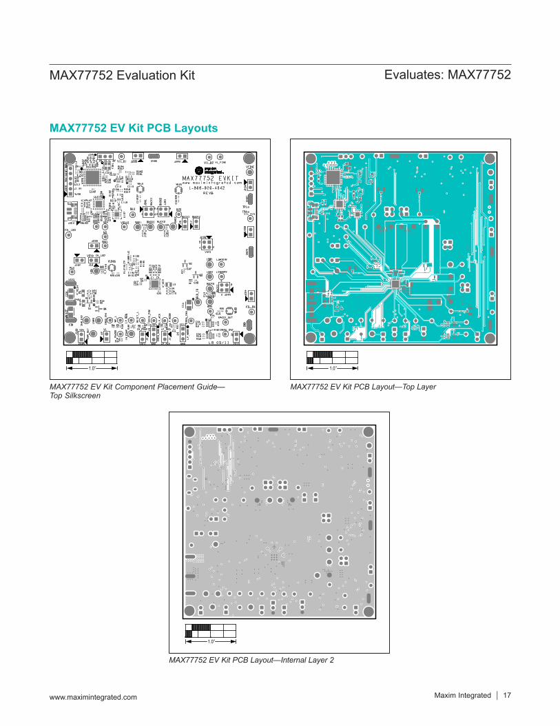
MAX77752 EV Kit Component Placement Guide— Top Silkscreen
MAX77752 EV Kit PCB Layout—Internal Layer 2
MAX77752 EV Kit PCB Layout—Top Layer
MAX77752 EV Kit PCB Layouts
1.0’’
1.0’’
1.0’’

Maxim Integrated │ 18www.maximintegrated.com
Evaluates: MAX77752MAX77752 Evaluation Kit
MAX77752 EV Kit PCB Layout—Internal Layer 3
MAX77752 EV Kit Component Placement Guide— Bottom Silkscreen
MAX77752 EV Kit PCB Layout—Bottom Layer
MAX77752 EV Kit PCB Layouts (continued)
1.0’’
1.0’’
1.0’’
Maxim Integrated cannot assume responsibility for use of any circuitry other than circuitry entirely embodied in a Maxim Integrated product. No circuit patent licenses are implied. Maxim Integrated reserves the right to change the circuitry and specifications without notice at any time.
Maxim Integrated and the Maxim Integrated logo are trademarks of Maxim Integrated Products, Inc. © 2017 Maxim Integrated Products, Inc. │ 19
Evaluates: MAX77752MAX77752 Evaluation Kit
Revision HistoryREVISIONNUMBER
REVISIONDATE DESCRIPTION PAGES
CHANGED
0 10/17 Initial release —
For pricing, delivery, and ordering information, please contact Maxim Direct at 1-888-629-4642, or visit Maxim Integrated’s website at www.maximintegrated.com.


![8 Eigenvectors and the Anisotropic Multivariate Gaussian …jrs/189s17/lec/08.pdf · 2017. 2. 14. · 777 777 777 777 777 5 [diagonal matrix of eigenvalues] Defn. of “eigenvector”:](https://img.pdfslide.net/doc/110x75/61216a6db677231115104a22/8-eigenvectors-and-the-anisotropic-multivariate-gaussian-jrs189s17lec08pdf.jpg)
![8 Eigenvectors and the Anisotropic Multivariate Normal …jrs/189/lec/08.pdf · 2021. 2. 18. · 777 777 777 777 777 5 [diagonal matrix of eigenvalues] Defn. of “eigenvector”:](https://img.pdfslide.net/doc/110x75/61216d94413a4f35294f60ea/8-eigenvectors-and-the-anisotropic-multivariate-normal-jrs189lec08pdf-2021.jpg)