Embed Size (px)
Citation preview

CLOCK AND DATA RECOVERY CIRCUITS
By
RUIYUAN ZHANG
A dissertation submitted in partial fulfillment of the requirements for the degree of
DOCTER OF PHILOSOPHY
WASHINGTON STATE UNIVERSITY School of Electrical Engineering and Computer Science
AUGUST 2004
ii
To the Faculty of Washington State University:
The members of the Committee appointed to examine the dissertation of
RUIYUAN ZHANG find it satisfactory and recommend that it be accepted.
(Chair)
iii
ACKNOWLEDGMENT
I would first like to thank my husband, Zhihe Zhou, for all his love, support and
understanding over years of this project. My deepest thanks are to Dr. George LaRue, my
advisor, for his professionalism and patience. I am motivated by his strong work ethic,
his creativity and his encouragement to be the best researcher I can become. Finally to the
rest of my committee, Dr. John Ringo and Dr. Deuk Heo, I extend my thanks for
providing additional expertise and support.
This work was supported in part by the NSF Center for the Design of Analog-
Digital Integrated Circuits (CDADIC).
iv
CLOCK AND DATA RECOVERY CIRCUITS
ABSTRACT
by Ruiyuan Zhang, Ph.D. Washington State University
August 2004
Chair: George S. LaRue
Clock and data recovery circuits (CDRs) have been widely used in data
communication systems. This dissertation presents a half-rate clock and data recovery
circuit that combines the best features, fast acquisition and low jitter, of digital phase
selection and phase locked loop CDR circuits. This CDR circuit consists of a phase
selector, which can lock to the data in just a few clock cycles but has high jitter, and a
PLL, which requires a much longer acquisition time but provides a low-jitter clock after
locking. Measurements in 0.5 µm CMOS technology show operation up to 700 Mbps, a
7% acquisition range, an initial acquisition time of 8 bit times with jitter of 30% bit time,
and jitter of 16 ps after the PLL acquires lock in about 700 ns from an initial frequency
difference of 7%.
A phase frequency magnitude detector (PFMD) is added to the combined CDR to
improve the acquisition time by feeding back an estimate of the magnitude of the
frequency offset in addition to the sign. Measurements show that the 700ns acquisition
time is reduced by about a factor of 5 to 140ns from an initial 7% frequency difference.
This dissertation also presents an analog version of the PFMD CDR in the 0.25
µm CMOS technology without the entire overhead associated with the phase selector
CDR in order to reduce power dissipation and area compared to the combined CDR.
v
TABLE OF CONTENTS
ACKNOWLEDGMENT................................................................................................ iii
ABSTRACT .................................................................................................................. iv
LIST OF TABLES........................................................................................................ vii
LIST OF FIGURES ......................................................................................................viii
CHAPTER...................................................................................................................... 1
1. INTRODUCTION .................................................................................................. 1
2. BACKGROUND .................................................................................................... 4
2.1 Phase Locked Loop ........................................................................................... 4
2.1.1 Basic topology of a PLL ............................................................................. 4
2.1.2 Charge-pump PLL ...................................................................................... 9
2.1.3 Jitter vs. phase noise ................................................................................. 13
2.1.4 Applications ............................................................................................. 19
2.2 Delay locked loop (DLL)................................................................................. 23
2.3 Combined delay and phase locked loop CDR .................................................. 26
2.4 Combined CDR with fast acquisition and low jitter ......................................... 28
3. COMBINED CDR WITH FAST ACQUISITION AND LOW JITTER................. 30
3.1 Phase locked loop............................................................................................ 31
3.2 Phase Selector ................................................................................................. 38
3.3 Combined CDR with PFD ............................................................................... 43
3.4 Combined CDR with PFMD............................................................................ 46
3.5 Analog implementation of PFMD.................................................................... 51
vi
4. MEASUREMENT RESULTS............................................................................... 58
4.1 Measurement Methods .................................................................................... 59
4.2 Acquisition time and jitter of the phase selector............................................... 64
4.3 Acquisition time of the combined CDR with PFD ........................................... 66
4.4 Acquisition time of the combined CDR with PFMD ........................................ 69
4.5 Output waveforms and jitter of the CDR.......................................................... 79
5. CONCLUSION..................................................................................................... 82
BIBLIOGRAPHY......................................................................................................... 85
APPENDIX .................................................................................................................. 89
A. Measurement Results of the Combined PFD CDR................................................ 89
B. Measurement Results of the PFMD CDR............................................................ 110
vii
LIST OF TABLES
TABLE 1 COUNTER NUMBER, MAGNITUDE OF CURRENT PULSE VERSUS FREQUENCY OFFSET
.............................................................................................................................. 47
TABLE 2 PERFORMANCE SUMMARY MEASURED VERSUS SIMULATED................................ 81

viii
LIST OF FIGURES
FIG. 1 SIMPLIFIED BLOCK DIAGRAM OF A DIGITAL RECEIVER ............................................. 1
FIG. 2 BASIC PHASE LOCKED LOOP ................................................................................... 4
FIG. 3 LINEAR MODEL OF THE PLL................................................................................... 5
FIG. 4 CHARGE-PUMP PLL............................................................................................... 9
FIG. 5 LINEAR MODEL OF CHARGE-PUMP PLL................................................................... 9
FIG. 6 OSCILLATOR POWER SPECTRUM ........................................................................... 14
FIG. 7 PHASE NOISE L(∆F ) PLOT OF THE OSCILLATOR ..................................................... 15
FIG. 8 BLOCK DIAGRAM OF THE PLL WITH PHASE NOISE ................................................. 17
FIG. 9 PHASE NOISE OF PLL........................................................................................... 18
FIG. 10 A QUADRICORRELATOR PLL.............................................................................. 21
FIG. 11 DIGITAL IMPLEMENTATION OF QUADRICORRELATOR........................................... 21
FIG. 12 A TYPICAL DELAY LOCKED LOOP........................................................................ 23
FIG. 13 THE LINEAR MODEL OF THE DELAY LOCKED LOOP ............................................... 24
FIG. 14 A PHASE SELECTION BASED DLL CDR............................................................... 25
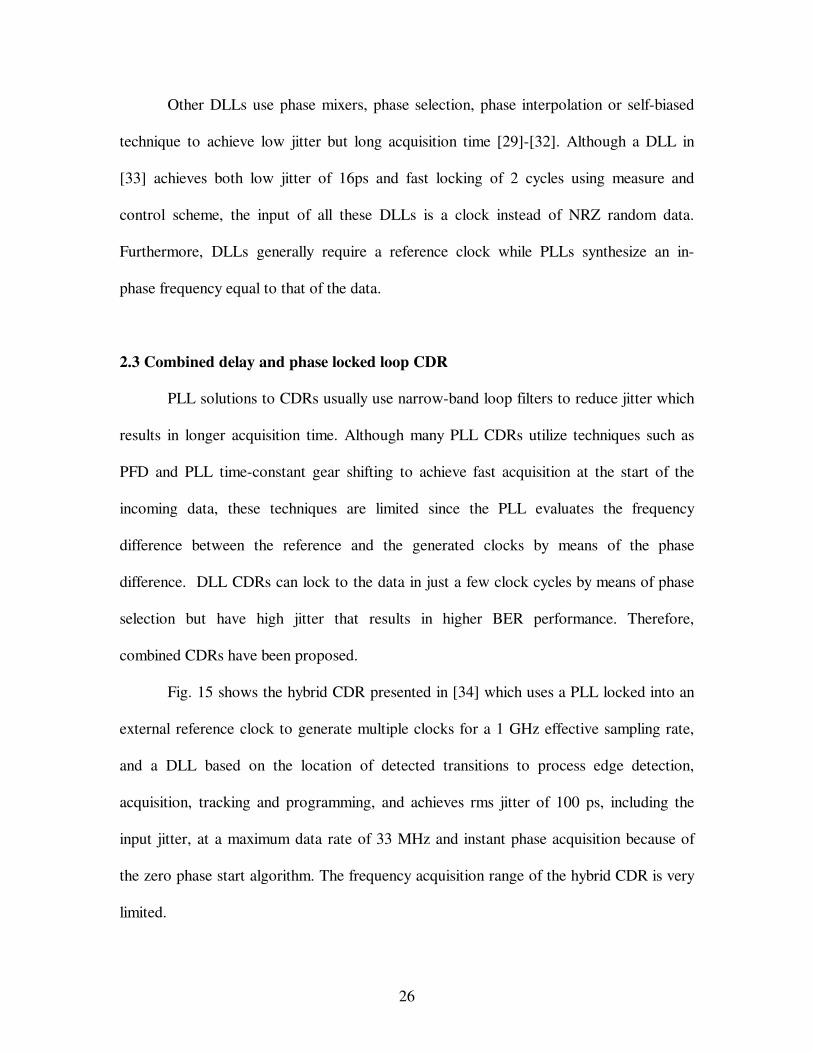
FIG. 15 HYBRID CDR .................................................................................................... 27
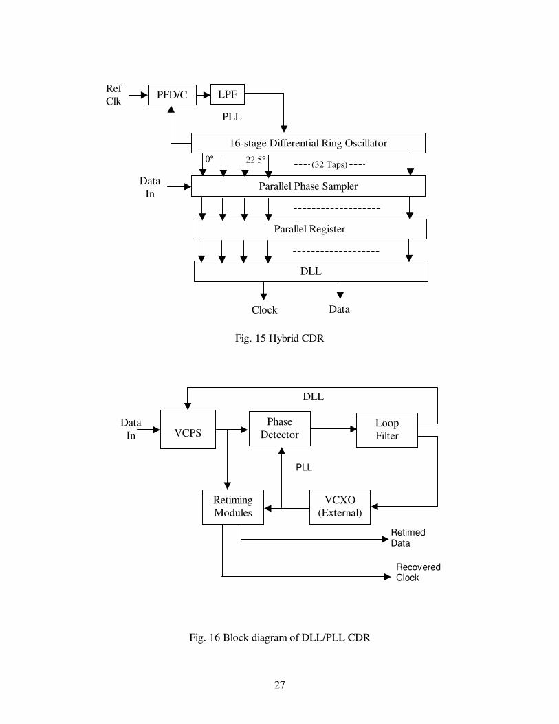
FIG. 16 BLOCK DIAGRAM OF DLL/PLL CDR ................................................................. 27
FIG. 17 COMBINED PS/PLL CDR................................................................................... 30
FIG. 18 PHASE LOCKED LOOP ......................................................................................... 31
FIG. 19 HALF-RATE PHASE DETECTOR ............................................................................ 32
FIG. 20 CHARGE PUMP ................................................................................................... 33
FIG. 21 VCO................................................................................................................. 34
FIG. 22 DUTY-CYCLE CORRECTOR.................................................................................. 35

ix
FIG. 23 SIMULATED JITTER HISTOGRAM OF PLL AT 800 MBPS ........................................ 36
FIG. 24 PLL SCHEMATIC............................................................................................... 37
FIG. 25 MULTIPLE CLOCK PHASES VERSUS DATA............................................................. 38
FIG. 26 PHASE SELECTOR BLOCK DIAGRAM..................................................................... 39
FIG. 27 OPERATION OF PHASE SELECTOR ........................................................................ 42
FIG. 28 CHARGE PUMP FOR FREQUENCY DETECTION ....................................................... 43
FIG. 29 WAVEFORMS FROM COMBINED CDR WITH PFD ................................................. 45
FIG. 30 COMPARISON OF ACQUISITION TIME ................................................................... 46
FIG. 31 DIGITAL LOGIC IMPLEMENTATION OF THE LOOK-UP TABLE .................................. 48
FIG. 32 PFMD CHARGE PUMP ........................................................................................ 48
FIG. 33 WAVEFORMS FROM THE PFMD SIMULATION...................................................... 49
FIG. 34 ACQUISITION TIME OF COMBINED CDR WITH PFMD AND WITH PFD .................. 50
FIG. 35 CHIP LAYOUT .................................................................................................... 51
FIG. 36 DIGITAL LOGIC GENERATING THE PHASE STATES................................................. 52
FIG. 37 ANALOG PFMD ................................................................................................ 53
FIG. 38 WAVEFORMS FROM ANALOG PFMD SIMULATION............................................... 54
FIG. 39 VCO CONTROL VOLTAGE OF THE ANALOG PFMD CDR ..................................... 55
FIG. 40 JITTER HISTOGRAM OF RECOVERED CLOCK FROM ANALOG PFMD CDR .............. 56
FIG. 41 LAYOUT OF THE ANALOG PFMD CDR ............................................................... 57
FIG. 42 CHIP MICROGRAPH OF THE COMBINED CDR........................................................ 58
FIG. 43 THE PROBE STATION .......................................................................................... 59
FIG. 44 THE MEASUREMENT SETUP................................................................................. 60
FIG. 45 CLOCK WAVEFORM............................................................................................ 61

x
FIG. 46 OVERLAIN CLOCK WAVEFORM IN ONE CYCLE...................................................... 62
FIG. 47 HISTOGRAM OF CALCULATED CLOCK CYCLE PERIOD ........................................... 63
FIG. 48 DEMULTIPLEXED DATA OUTPUT OF PHASE SELECTOR .......................................... 64
FIG. 49 RECOVERED CLOCK JITTER MEASUREMENT OF PHASE SELECTOR.......................... 65
FIG. 50 THE ACQUISITION BIT TIMES OF THE PHASE SELECTOR IN THE PFD CDR.............. 66
FIG. 51 CYCLE PERIOD OF THE RECOVERED CLOCK FROM PFD CDR AT DATA RATE 650
MBPS..................................................................................................................... 67
FIG. 52 PHASE DIFFERENCE MEASURED FROM PFD CDR AT DATA RATE 650 MPBS ......... 68
FIG. 53 COMPARISON OF ACQUISITION TIMES BETWEEN PLL AND PS IN THE COMBINED
PFD CDR.............................................................................................................. 69
FIG. 54 COMPARISON OF ACQUISITION BIT TIMES OF PS BETWEEN PFMD CDR AND PFD
CDR...................................................................................................................... 70
FIG. 55 CYCLE PERIOD OF THE RECOVERED CLOCK FROM THE PFMD CDR AT DATA RATE
700 MBPS .............................................................................................................. 71
FIG. 56 PHASE DIFFERENCES OF THE RECOVERED CLOCK FROM PFMD CDR AT DATA RATE
700 MBPS .............................................................................................................. 72
FIG. 57 ACQUISITION TIMES OF THE PLL IN THE PFMD CDR WITH VCO INITIALLY AT 645
MBPS..................................................................................................................... 73
FIG. 58 HISTOGRAM OF THE PLL ACQUISITION TIME OF THE 50 SAMPLES AT DATA RATE OF
700 MBPS .............................................................................................................. 74
FIG. 59 CYCLE PERIOD OF THE RECOVERED CLOCK IN THE WORST CASE........................... 75
FIG. 60 PHASE DIFFERENCE IN THE WORST CASE ............................................................. 75

xi
FIG. 61 ACQUISITION TIMES OF THE PLL IN THE PFMD CDR WITH VCO INITIALLY AT 550
MBPS..................................................................................................................... 76
FIG. 62 ACQUISITION TIMES OF THE PLL AND PHASE SELECTOR IN THE COMBINED PFMD
CDR...................................................................................................................... 77
FIG. 63 PLL ACQUISITION TIMES OF THE PFMD CDR AND THE PFD CDR...................... 78
FIG. 64 RECOVERED DATA AND CLOCK OUTPUT .............................................................. 79
FIG. 65 JITTER HISTOGRAM OF THE RECOVERED CLOCK................................................... 80
FIG. 66 JITTER HISTOGRAM MEASURED FROM DIGITAL OSCILLOSCOPE ............................. 80
FIG. A1 CYCLE PERIOD OF THE RECOVERED CLOCK FROM THE PFD CDR AT DIFFERENT
DATA RATES........................................................................................................... 89
FIG. A2 PHASE DIFFERENCE MEASURED FROM THE PFD CDR AT DIFFERENT DATA RATES
............................................................................................................................ 100
FIG. B1 CYCLE PERIODS OF THE RECOVERED CLOCK FROM THE PFMD CDR AT DIFFERENT
DATA RATES......................................................................................................... 110
FIG. B2 PHASE DIFFERENCES MEASURED FROM PFMD CDR AT DIFFERENT DATA RATES121

xii
Dedication
To my parents
To my husband, Zhihe and my son, Kevin
1
CHAPTER ONE
INTRODUCTION
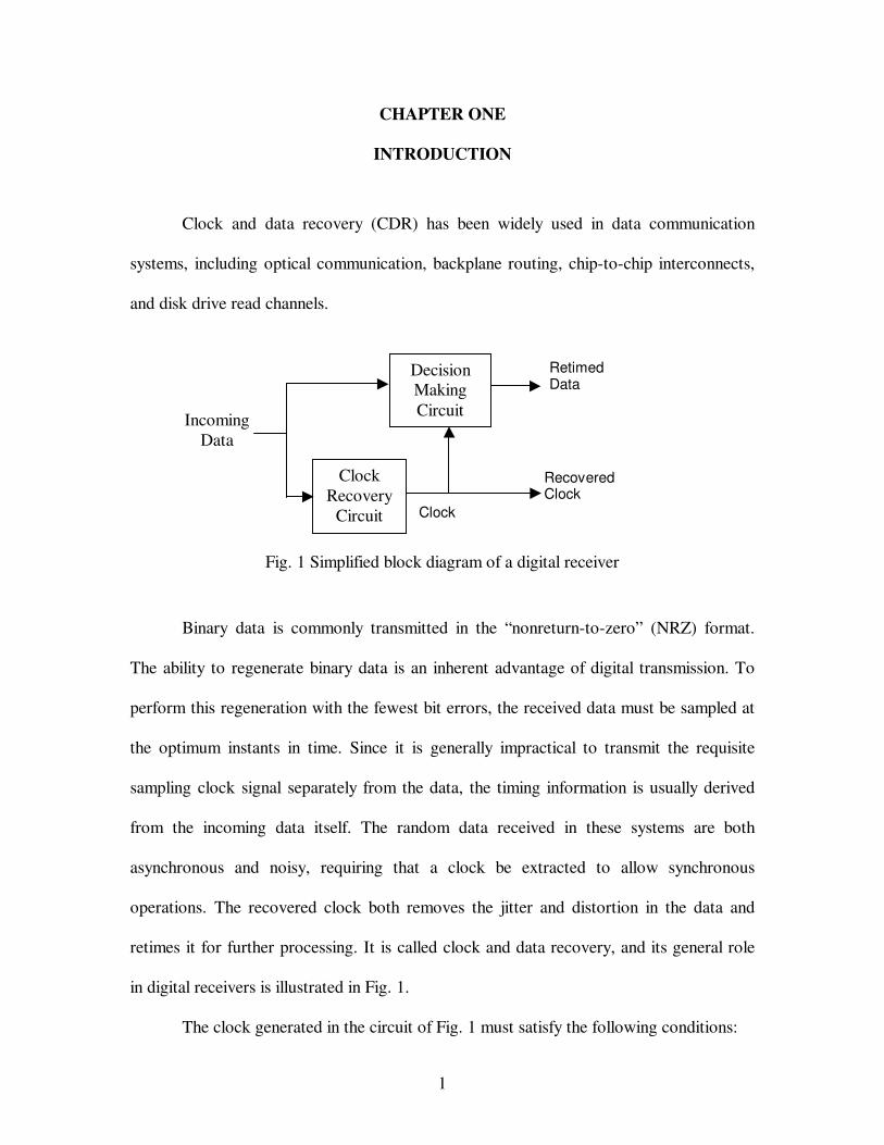
Clock and data recovery (CDR) has been widely used in data communication
systems, including optical communication, backplane routing, chip-to-chip interconnects,
and disk drive read channels.
Fig. 1 Simplified block diagram of a digital receiver
Binary data is commonly transmitted in the “nonreturn-to-zero” (NRZ) format.
The ability to regenerate binary data is an inherent advantage of digital transmission. To
perform this regeneration with the fewest bit errors, the received data must be sampled at
the optimum instants in time. Since it is generally impractical to transmit the requisite
sampling clock signal separately from the data, the timing information is usually derived
from the incoming data itself. The random data received in these systems are both
asynchronous and noisy, requiring that a clock be extracted to allow synchronous
operations. The recovered clock both removes the jitter and distortion in the data and
retimes it for further processing. It is called clock and data recovery, and its general role
in digital receivers is illustrated in Fig. 1.
The clock generated in the circuit of Fig. 1 must satisfy the following conditions:
Decision Making Circuit
Clock Recovery
Circuit
Incoming Data
Retimed Data
Recovered Clock
Clock
2
• The frequency of the clock must be equal to the data rate.
• The clock must have appropriate timing with respect to the data, allowing
optimum sampling of the data by the clock; if the rising edges of the clock occur
in the midpoint of each bit, the sampling occurs farthest from the data transitions,
providing maximum margin for jitter and other time uncertainty.
• The clock must exhibit a small jitter since the jitter of the clock contributes to the
retimed data jitter [1].
Both phase locked loop (PLL) and delay locked loop (DLL) have been widely
used in clock and data recovery. PLL solutions to CDR usually use narrow-band loop
filters to reduce jitter which results in longer acquisition times. Usually this is in the ½ to
1 microsecond range. If the jitter is low, less coding is needed to reduce the number of
bit errors. DLL CDRs can lock to the data in just a few clock cycles by means of phase
selection but have high jitter that results in higher bit error rate. Thus, more coding
overhead is needed to reduce the number of bit errors. Therefore, there are tradeoffs
between fast acquisition and low jitter.
For networks with fast switching between nodes, short acquisition time reduces
the number of preamble bits required and results in higher efficiency. Low jitter is
important for low bit-error rate (BER) in the transfer of data. Both low jitter and short
acquisition time are difficult to achieve simultaneously. PLL CDRs have higher
efficiency than DLL CDRs for long connection times since the lower coding overhead
makes up for the extra ½ to 1 microsecond of acquisition time. DLL CDRs have higher
efficiency for short connection times since they can start transferring data almost
instantly.
3
This dissertation presents a combined phase selector / PLL CDR which consists of
a phase selector (PS), which can lock to the data in just a few clock cycles but has high
jitter, and a PLL, which requires a much longer acquisition time but provides a low-jitter
clock after locking. For any connection time, the combined CDR has a data transfer
efficiency that is higher than or equal to the maximum of the PLL CDR or the DLL CDR.
For short connection times, the combined CDR is equal to the DLL CDR since the PLL
does not have time to lock. For longer connection times, the additional coding can be
removed and the efficiency of the combined CDR is higher than the DLL. For very long
connection times, the extra ½ to 1 microsecond of data transferred does not add
significantly to the efficiency achieved by the PLL CDR. The drawbacks of the combined
CDR is that more layout area and power dissipation results from the additional circuitry
needed. A novel phase frequency magnitude detector (PFMD) is also introduced to
substantially reduce the PLL acquisition time. This will allow a further increase in data
transfer efficiency.
Since many applications don’t need the instant acquisition of the phase selector
but can still benefit from the fast PLL acquisition of PFMD CDR, this dissertation also
presents the analog implementation of a PFMD CDR without the entire overhead
associated with the phase selector of the combined CDR in order to reduce power
dissipation and area.
Chapter Two provides a general background on clock and data recovery. Chapter
Three describes the designs of the PLL and phase selector circuits, the digit and analog
implementation of PFMD, and presents the simulation results. In Chapter Four,
measurement results are discussed. Chapter Five is the conclusion.
4
CHAPTER TWO
BACKGROUND
In many systems, data are transmitted or retrieved without any additional time
reference, but the receiver must eventually process the data synchronously. Thus, the
time information (e.g. clock) must be recovered from the data at the receive end. The
common ways to recover the clock are with a phase locked loop or a delay locked loop
(DLL).
2.1 Phase Locked Loop
A PLL is a feedback system that operates on the excess phase of nominally
periodic signals. The basic topologies and a number of important parameters are
discussed for better understanding [2].
2.1.1 Basic topology of a PLL
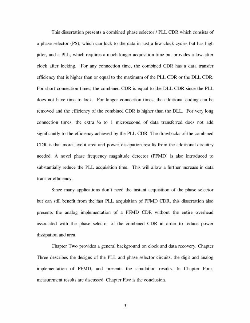
Fig. 2 Basic phase locked loop
Shown in Fig. 2 is a simple PLL which consists of a phase detector (PD), a low-
pass filter (LPF), and a voltage controlled oscillator (VCO). In the locked condition, all
the signals in the loop have reached a steady state and the PLL operates as follows. The
Phase Detector
Low-Pass Filter VCO x(t) y(t)
5
phase detector produces an output whose dc value is proportional to the phase difference
φ∆ between x(t) and y(t). The low-pass filter suppresses high-frequency components in
the PD output, allowing the dc value to control the VCO frequency. The VCO then
oscillates at a frequency equal to the input frequency and with a phase difference equal to
φ∆ . Thus, the LPF generates the proper control voltage for the VCO.
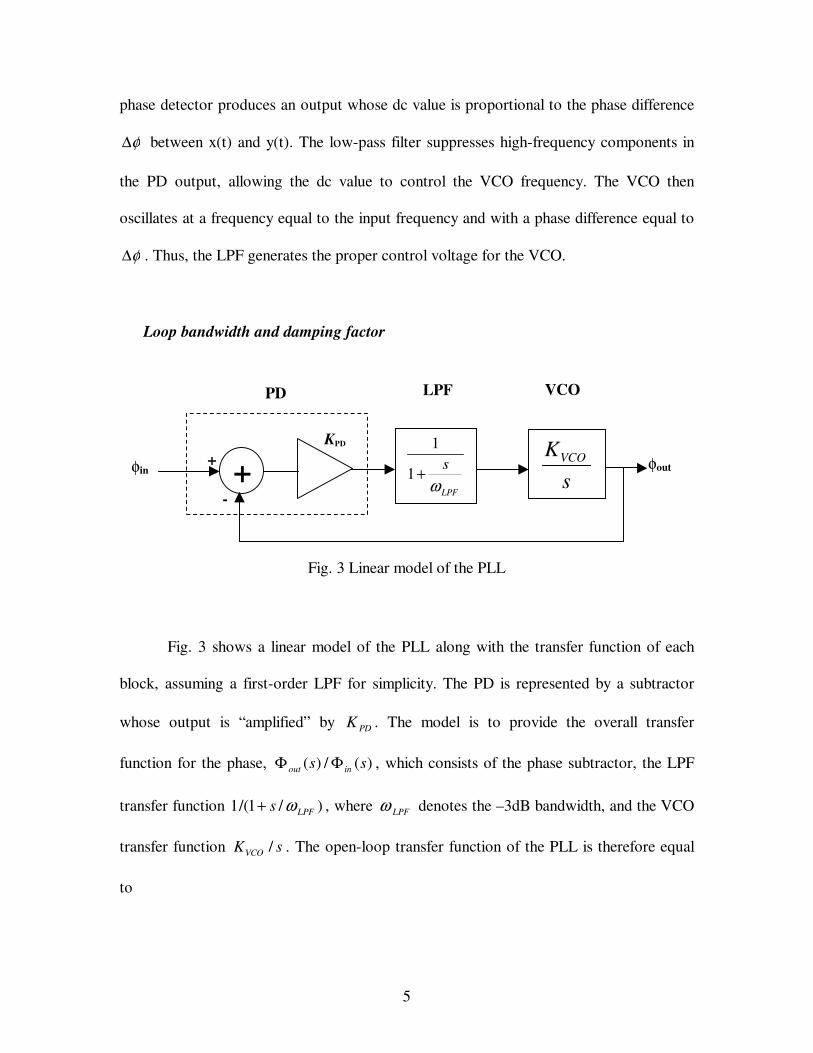
Loop bandwidth and damping factor
Fig. 3 Linear model of the PLL
Fig. 3 shows a linear model of the PLL along with the transfer function of each
block, assuming a first-order LPF for simplicity. The PD is represented by a subtractor
whose output is “amplified” by PDK . The model is to provide the overall transfer
function for the phase, )(/)( ss inout ΦΦ , which consists of the phase subtractor, the LPF
transfer function )/1/(1 LPFs ω+ , where LPFω denotes the –3dB bandwidth, and the VCO
transfer function sKVCO / . The open-loop transfer function of the PLL is therefore equal
to
LPF
sω
+1
1
s
KVCO+
PD LPF VCO
KPD +
-
φin φout
6
s
Ks
KsH VCO
LPF
PDopen ⋅+
⋅=
ω1
1)( , (2.1)
revealing one pole at LPFs ω−= and another at 0=s . Note that the loop gain is equal to
opensH )( because of the unity feedback factor. Since the loop gain contains a pole at the
origin, the system is called a “type I” PLL.
From the open-loop transfer function the closed-loop transfer function is
VCOPDLPF
VCOPD
open
open
in
out
KKss
KKsH
sH
ss
sH++
=+
=ΦΦ
=
ω
2)(1
)(
)()(
)( (2.2)
We convert the denominator of Equation (2.2) to the familiar form used in control
theory, 22 2 nn ss ωξω ++ , where ξ is the damping factor and nω is the natural frequency.
Thus,
22
2
2)(
nn
n
sssH
ωξωω
++= (2.3)
where
VCOPDLPFn KKωω = (2.4)
VCOPD
LPF
KKωξ
21= (2.5)
Note that nω is the “natural frequency” and ξ is the “damping factor”. ξ is
usually greater than 0.5 and preferably equal to 2/2 so as to provide an optimally flat
frequency response. Therefore, VCOPD KK and LPFω cannot be chosen independently.
These limitations translate to significant phase error between the input and the output as
well as a narrow capture range.
7
Track range
The tracking behavior is distinctly different in two different cases: 1) the input
frequency varies slowly (static tracking), and 2) the input frequency is changed abruptly
(dynamic tracking).
In the first case, the input frequency varies slowly such that the difference
between inω and outω always remains much less than LPFω . The PLL tracks as long as
the magnitude of the VCO control voltage varies monotonically. The edge of the tracking
range is reached at the point where the gain of the PD or the gain of the VCO drops
sharply or changes sign.
Capture (acquisition) range
In the second case mentioned above, with an input frequency step at its input, the
PLL loses lock, at least temporarily. There are two similar situations: 1) a loop initially
locked at iniω experiences a large input frequency step, ω∆ ; and 2) a loop initially
unlocked and free running at iniω must lock onto an input frequency given by
ωωω ∆=− iniin . In both situations, the loop must acquire lock. The acquisition range
(also called the capture range) is the maximum value of ω∆ for which the loop locks.
Acquisition range is a critical parameter because 1) it trades directly with the loop
bandwidth. The acquisition range depends on how much the LPF passes the component at
ω∆ and how strong the dc feedback component is; 2) the acquisition range determines
the maximum frequency variation in the input or the VCO that can be accommodated. In
monolithic implementations, the VCO free-running frequency can vary substantially with
temperature and process, thereby requiring a wide acquisition range even if the input
8
frequency is tightly controlled.
Acquisition time
The acquisition time and settling time of PLLs, which are inversely proportional
to nξω , are important in many applications. For a simple second-order PLL, the
acquisition time is inversely proportional to LPFω . In fact, nonlinearities in PDK and
VCOK result in different settling characteristics, and simulations must be used to predict
the acquisition time accurately.
Jitter
Another important issue in PLL designs is jitter. “Cycle-to-cycle” jitter is often
used to describe the performance of a PLL, which is the difference between every two
consecutive periods of an almost-periodic waveform. Two jitter phenomena in PLLs are
of great interest: (a) the input exhibits jitter, and (b) the VCO produces jitter. The
response of the PLL to these two types of jitter is different. To suppress the jitter caused
by additive noise in the input, the PLL should be designed so that the noise bandwidth of
the PLL is minimized. This means smaller loop gain, which causes narrow noise
bandwidth. On the other hand, in order to suppress the jitter caused by the noise
generated in the PLL itself, the operation of the PLL needs to be stable. The output jitter
due to PLL circuits is inversely proportional to the loop gain. In other words, larger loop
gain can reduce the jitter caused by the noise in the CDR.

9
2.1.2 Charge-pump PLL
Many modern applications use a charge-pump PLL due to the trade-off between
ξ and LPFω in the simple PLL shown in Fig. 2 [40]. Charge-pump PLLs incorporate a
phase detector and a charge pump (Fig. 4) instead of the combinational PD and the LPF
in Fig. 2. In order to stabilize the system, a resistor is added in series with the loop filter
capacitor to introduce a zero in the loop gain.
PFD VCO
IP
RP
CP
VDD
x(t)y(t)
Fig. 4 Charge-pump PLL
The linear model of the charge-pump PLL is shown in Fig. 5.
Fig. 5 Linear model of charge-pump PLL
+
PP
P
sCR
I 12π s
KVCO
+
PD/CP/LPF VCO
+
-
φin
PD
IP
10
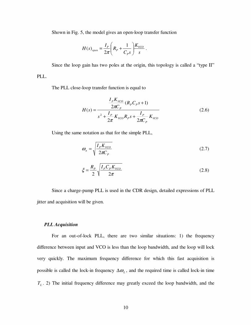
Shown in Fig. 5, the model gives an open-loop transfer function
s
KsC
RI
sH VCO
PP
Popen
+= 1
2)(
π.
Since the loop gain has two poles at the origin, this topology is called a “type II”
PLL.
The PLL close-loop transfer function is equal to
VCOP
PPVCO
P
PPP
VCOP
KC
IsRK
Is
sCRC
KI
sH
ππ
π
22
)1(2
)(2 ++
+= (2.6)
Using the same notation as that for the simple PLL,
P
VCOPn C
KIπ
ω2
= (2.7)
π
ξ22
VCOPPP KCIR= (2.8)
Since a charge-pump PLL is used in the CDR design, detailed expressions of PLL
jitter and acquisition will be given.
PLL Acquisition
For an out-of-lock PLL, there are two similar situations: 1) the frequency
difference between input and VCO is less than the loop bandwidth, and the loop will lock
very quickly. The maximum frequency difference for which this fast acquisition is
possible is called the lock-in frequency Lω∆ , and the required time is called lock-in time
LT . 2) The initial frequency difference may greatly exceed the loop bandwidth, and the

11
VCO frequency will slowly walk in toward the input frequency. The maximum frequency
difference from which the loop will eventually lock is called the acquisition range pω∆
(pull-in frequency), and the required time is called acquisition time (pull-in time) PT
[38].
The lock-in frequency can be expressed as
πξωω
22 VCOPP
nL
KIR=≈∆ (2.9)
The lock-in time LT is on the order of nω
1 seconds.
The acquisition range can be given approximately by [39]
vnp Kξωπ
ω 8≈∆ for vn K>>ω (2.10)
where vK is equal to VCOp K
I
π2. A narrow-band loop has a small acquisition
range.
The acquisition time is given approximately by
( )
3
2
2 nPT
ξωω∆≈ (2.11)
A narrow-band loop can take a long time to pull in. Therefore, the acquisition
range increases with nω while the acquisition time decreases with nω .
PLL jitter
Two types of jitter in a PLL are of great interest: ( I ) jitter caused by additive
noise in the input signal , and ( II ) jitter caused by noise generated in the VCO [37].
12
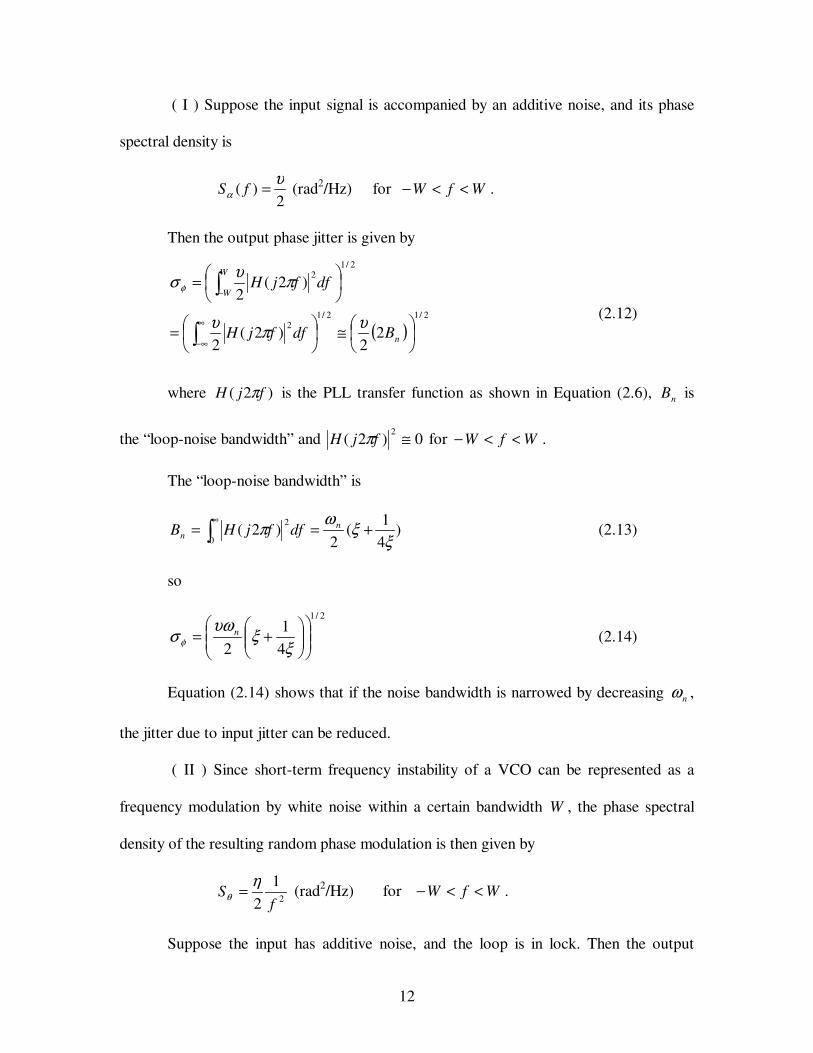
( I ) Suppose the input signal is accompanied by an additive noise, and its phase
spectral density is
2
)(υ
α =fS (rad2/Hz) for WfW <<− .
Then the output phase jitter is given by
( )2/12/1
2
2/12
22
)2(2
)2(2
≅
=
=
∞
∞−
−
n
W
W
BdffjH
dffjH
υπυ
πυσ φ
(2.12)
where )2( fjH π is the PLL transfer function as shown in Equation (2.6), nB is
the “loop-noise bandwidth” and 0)2(2 ≅fjH π for WfW <<− .
The “loop-noise bandwidth” is
)41
(2
)2(0
2
ξξωπ +==
∞ nn dffjHB (2.13)
so
2/1
41
2
+=
ξξυωσ φ
n (2.14)
Equation (2.14) shows that if the noise bandwidth is narrowed by decreasing nω ,
the jitter due to input jitter can be reduced.
( II ) Since short-term frequency instability of a VCO can be represented as a
frequency modulation by white noise within a certain bandwidth W , the phase spectral
density of the resulting random phase modulation is then given by
2
12 f
Sη
θ = (rad2/Hz) for WfW <<− .
Suppose the input has additive noise, and the loop is in lock. Then the output
13
phase jitter caused by VCO phase modulation is given by
( )
2/12
2/1
2
2
2
21
2
=
−= −
n
W
Wdf
f
fjH
ξωπη
πησ θ
. (2.15)
In this equation, the jitter is inversely proportional to nω . In other words, jitter
caused by noise generated in the PLL reduces as nω increases.
For clock recovery applications there is usually a significant amount of jitter in
the input signal as well as the VCO. Thus, there is a trade-off in the choice of the loop
bandwidth. To suppress the jitter caused by additive noise in the input, the PLL should be
designed so that the noise bandwidth of the PLL is minimized and the loop will not try to
track input fluctuation strongly. On the other hand, this means the narrow bandwidth PLL
does not correct VCO timing errors as quickly. The narrow bandwidth also results in
smaller acquisition range and larger acquisition time.
2.1.3 Jitter vs. phase noise
Phase noise and jitter are different ways of quantifying the same phenomenon.
Jitter is a measurement of the variations in the time domain, and essentially describes
how far the signal period has varied from its ideal value. Phase noise is another measure
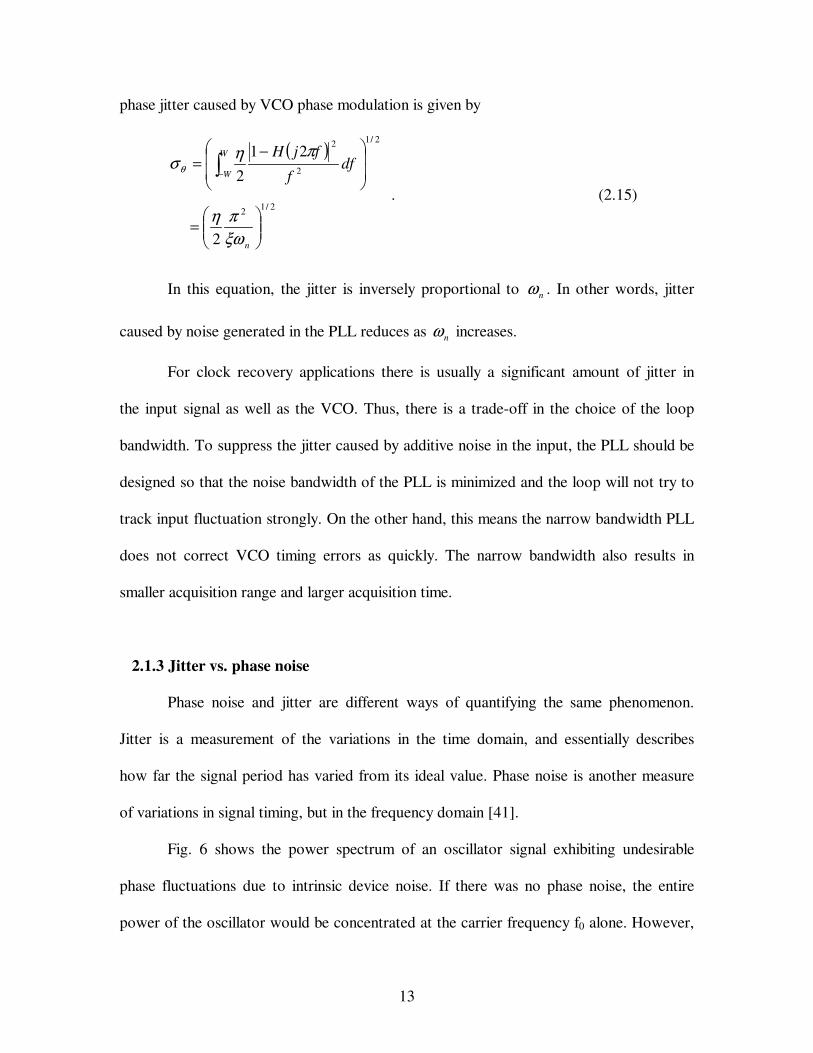
of variations in signal timing, but in the frequency domain [41].
Fig. 6 shows the power spectrum of an oscillator signal exhibiting undesirable
phase fluctuations due to intrinsic device noise. If there was no phase noise, the entire
power of the oscillator would be concentrated at the carrier frequency f0 alone. However,
14
phase noise spreads some of the oscillator’s power to adjacent frequencies, which results
in sidebands. In Fig. 6, the sidebands are shown falling off at 1/∆f for low offset
frequencies ∆f from the carrier mainly due to device flicker noise and flatter for higher
offset frequencies where the behavior is dominated by the thermal noise in the devices of
the oscillator circuit.
Fig. 6 Oscillator power spectrum
Phase noise is represented as a ratio of power in 1Hz bandwidth in one sideband
to the power of the carrier, C
SSB
PP
, where SSBP is the power in one sideband and CP is the
SIDEBAND NOISE
CARRIER
f0 f0+∆∆∆∆f
PSSB PC
f
PC
PSSB
15
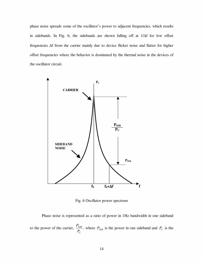
power of the carrier. Phase noise is usually specified in dBc/Hz at a frequency offset ∆f
from the carrier, where dBc is the level in dB relative to the carrier. Fig. 7 shows phase
noise of the oscillator. The spectrum in Fig.7 is also called the spectral density of phase
fluctuations. There are regions in the sidebands where the phase can vary as 1/f3 and 1/f2,
depending on the noise process involved. The 1/f2 region is referred to as the “white
frequency” variation region, since it is due to white, or uncorrelated, fluctuations in the
period of the oscillator caused by thermal noise. For low enough offset frequencies, the
flicker noise of devices comes to play and the spectrum in this region varies as 1/f3.
Fig. 7 Phase noise L(∆f ) plot of the oscillator
∆∆∆∆f
1 f 3
1 f 2
Noise Floor
L(∆∆∆∆f) dBc/Hz
16
Translating between phase noise and jitter
Since jitter and phase noise characterize the same phenomenon, it can be useful to
derive a jitter value from a phase noise measurement. This can be done as follows.
The phase noise L(∆f ) plot, as shown in Fig. 7 gives the single sideband noise
distribution in the form of a power spectral density function in units of dBc. The total
noise power N (dBc) of the single sideband can be determined by integrating the L(∆f )
function over the band of interest, from f1 to f2, as shown in Equation (2.16)
==2
1)()(
f
fdffLNoisePowerdBcN (2.16)
The RMS phase jitter caused by this noise power can be determined by
210)( 10 ×=N
radianφσ (2.17)
To convert to time, divide Eq (2.17) by the frequency of the carrier in radians, as
follows:
02
)((sec)
f
radiansRMSjitter
××=
πσ φ (2.18)
Relationship between phase noise and jitter for a PLL
When the VCO is free running (PLL open loop), the power spectral density (psd)
of the phase noise is shown in Fig. 7. Assuming the phase noise is dominated by
integrated white noise, the phase noise psd OPENSφ at the VCO output is modeled by
21)(
fN
fS OPEN =φ dBc/Hz (2.19)
where f is the offset frequency from the “carrier” (VCO free-running frequency)
17
and 1N is the noise power of the VCO.
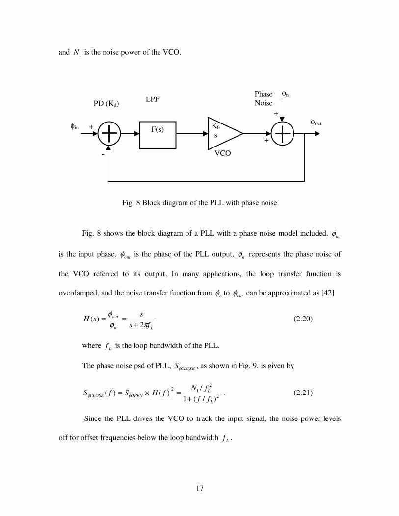
Fig. 8 Block diagram of the PLL with phase noise
Fig. 8 shows the block diagram of a PLL with a phase noise model included. inφ
is the input phase. outφ is the phase of the PLL output. nφ represents the phase noise of
the VCO referred to its output. In many applications, the loop transfer function is
overdamped, and the noise transfer function from nφ to outφ can be approximated as [42]
Ln
out
fss
sHπφ
φ2
)(+
== (2.20)
where Lf is the loop bandwidth of the PLL.
The phase noise psd of PLL, CLOSESφ , as shown in Fig. 9, is given by
2
212
)/(1/
)()(L
LOPENCLOSE ff
fNfHSfS
+=×= φφ . (2.21)
Since the PLL drives the VCO to track the input signal, the noise power levels
off for offset frequencies below the loop bandwidth Lf .
F(s) φin +
-
+
+
φn
K0
s
φout
PD (Kd) LPF
VCO
Phase Noise

18
Fig. 9 Phase noise of PLL
The phase noise psd in Equation (2.21) can be integrated over all frequencies to
give the average power of the jitter process, which gives the variance of jitter
performance, 2φσ :
212
21
)/(1/
φσπ==
+∞+
∞−LL
L
fN
dfff
fN (2.22)
where φσ is the rms phase jitter in units of radians. The rms jitter in units of time
gives
LfN
fRMSjitter
π41 1
0
= . (2.23)
Since the phase noise psd )( fS OPENφ in Equation (2.19) is given in units of
dBc/Hz, 1N is determined by
210/)(1 10 fN fS OPEN ×= φ (2.24)
where f is the offset frequency from the VCO free-running frequency.
f
fL
SΦΦΦΦ(f)
19
2.1.4 Applications
A number of approaches have been proposed for developing a CDR using the
PLL technique [3]-[8]. The advantage of the PLL CDR is that a PLL offers low clock
jitter after it acquires lock.
All of the building blocks in the PLL CDR of reference [3] are fully differential to
minimize the effect of supply and common-mode noise. This recovered clock exhibits an
rms jitter of 10.8 ps for 2.5 Gbps pseudo-random bit sequence (PRBS) NRZ data of
length 127 − .
The PLL CDR in [4] uses half-frequency clock because of the unusual phase
detector which uses a DLL to generate multiple sampling clocks. The clock jitter is about
350 ps at 1 Gbps with a 1215 − length data.
Reference [5] describes a 10 Gbps CMOS CDR which uses a linear phase
detector to compare the phase of the incoming data with that of a half-rate clock.
Compared to nonlinear bang-bang PDs, linear PDs generate a linearly proportional output
that drops to zero when the loop is locked, resulting in less charge pump activity, smaller
ripple on the oscillator control line, and hence lower jitter. The circuit exhibits an rms
jitter of 1 ps in the recovered clock with random data input of length 1232 − .
With long random pattern data input, the VCO control voltage is pulled back to its
natural frequency during the input of consecutive data bits, making the PLL more
unstable and resulting in larger output jitter. To stabilize the PLL with small output jitter,
the PLL CDR in [6] inserts a S/H switch between the phase comparator and the LPF. The
phase detector output signal can be transferred to the LPF only when the S/H switch is in
the sample mode. By setting the S/H switch in the hold mode during the consecutive data

20
period, the control voltage for the VCO can be kept constant to reduce the output jitter.
The CDR circuit demonstrated error-free operation with an input of 1232 − PRBS data at
156 Mbps.
The loop gain of the PLL can be adjusted to suppress different jitter sources. The
PLL CDR in [7]-[8] inserts a gain control amplifier (GCA) circuit to adjust the loop gain.
The design utilizes large loop gain to reduce the jitter caused by noise generated in the
CDR circuit and small loop gain to suppress the input jitter.
In most applications, the PLL CDRs concentrate on reducing the input jitter,
which requires a narrow loop bandwidth to meet the jitter transfer specification. This in
turn severely limits the capture range and acquisition time of the PLL. Therefore,
frequency detection is also necessary to guarantee lock in the presence of large oscillator
frequency variations. A phase frequency detector (PFD) significantly increases
acquisition range and lock speed of a PLL, compared to a conventional PLL with phase
detector only. Different PFD schemes for NRZ data have been proposed.
A number of CDR architectures are based on analog or digital implementation of
the “quadricorrelator” introduced by Richman [9] and modified by Bellisio [10]. The
analog implementation of the architecture is shown in Fig.10. The quadricorrelator,
which consists of Loop 1 and Loop 2, detects the frequency difference between the clock
frequency of the random input data and VCO free-running frequency. Once the frequency
lock has been established, the loop is dominated by Loop 3 and the feedback signal of the
frequency difference becomes a small offset signal. This technique prevents narrowing of
the acquisition range in a conventional single-loop PLL. At the same time, it can achieve
a low cut-off frequency of the jitter transfer curve by setting a narrow loop bandwidth of

21
Loop 3. The CDR circuit based on the analog quadricorrelator exhibits an rms jitter of
9.5ps and a capture range of 300 MHz at 2.5 Gbps [11].
Fig. 10 A quadricorrelator PLL
Q
QSET
CLR
D
Q
Q
SET
CLRD
Q
QSET
CLR
D
VCO LPF +NRZData
Fig. 11 Digital implementation of quadricorrelator
The quadricorrelator can also be realized in digital form. The architecture of Fig.
10 can be “digitalized” as shown in Fig. 11. Since the digital quadricorrelator works
Edge Detector
LPF
VCO LPF
LPF
××××
××××
×××× ××××
dtd
Loop 2
Loop 1 Loop 3
NRZ Data P
M

22
without signal preprocessing, internal filtering, and phase shifting, which are required for
the analog quadricorrelator approach, many CDR circuits utilize the quadricorrelator in
digital form [12]-[16]. The PFD IC in reference [12], which comprises a phase detector,
a quadrature phase detector and frequency detector, was fabricated in a 0.9 µm 12 GHz fT
silicon bipolar process. The measured rms jitter of the recovered clock is less than 1.9 ps
for a PRBS length of 223-1. The PFD concept in reference [13]-14] are based on the
architecture in reference [12]. The measured rms jitter of the CDR IC in [13] is 3.8 ps at
2.488 Gb/s. The CDR in [14] exhibits a measured rms clock jitter of 12.5 ps at 933 MHz.
In [16] the PFD consists of a phase detector in which in-phase and quadrature phases of a
half-rate clock signal sample the data in two double-edge-triggered flipflops and a
frequency detector. The CDR exhibits a measured rms clock jitter of 0.8 ps at 9.95328
Gb/s for a PRBS length of 223-1.
The duplicated loop control CDR in [17] consists of two-SF (switched filter)
CDRs to achieve about twice the acquisition range of a single loop CDR and an rms jitter
of 3.8ps at 2.5 Gbps. One loop (Loop F) has large loop gain and the other loop (Loop P)
has small gain. A CDR using only Loop P has narrow acquisition range, yet provides a
lower cut-off frequency of the jitter transfer curve. On the other hand, a CDR using only
Loop F has wide capture range and a higher cut-off frequency of the jitter transfer curve.
A PLL CDR in [18] with frequency detection achieves a wide acquisition range of
20% and jitter of 7.4ps. Other types of PFD for NRZ data are described in [19]-[22].
The PLL CDRs with PFD increase the capture range by adding frequency
detectors, but acquisition time is rather limited since the PFD used in a charge-pump PLL
estimates the frequency difference between the reference and the generated clocks by

23
means of the phase difference. A low-noise fast-lock PLL with adaptive bandwidth
control can lock in about 30 clock cycles with 20 ps peak-to-peak jitter [23]. However, it
uses a reference clock as input instead of random data.
2.2 Delay locked loop (DLL)
In applications where no clock synthesis is required, DLLs provide an attractive
alternative to generate multiple clock phases due to their fast acquisition time, low phase
error accumulation and better stability. Fig. 12 shows the block diagram of a typical delay
locked loop, which consists of a phase detector, charge pump, low pass filter and voltage
controlled delay line (VCDL). The delay through the VCDL is adjusted with negative
feedback in the loop by integrating the phase error that results between the input clock
and the delay line output. The VCDL provides multiple clock phases with adjusted delay.
Once in lock, the VCDL will delay the input clock by a certain amount of time so that
there is no detected phase error between the input clock and output. Therefore, the VCDL
delay must be a multiple of the input clock period.
Fig. 12 A typical delay locked loop
CP φin
φout
PD VCDL
Cp
24
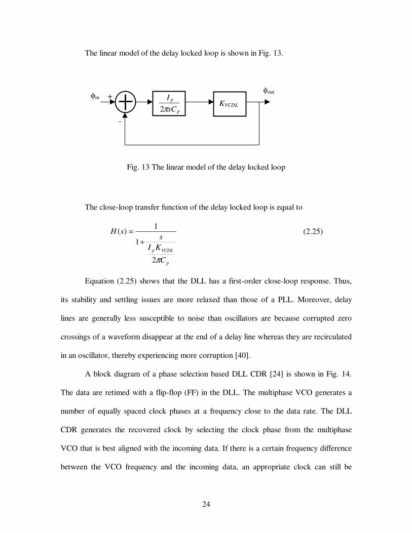
The linear model of the delay locked loop is shown in Fig. 13.
Fig. 13 The linear model of the delay locked loop
The close-loop transfer function of the delay locked loop is equal to
p
VCDLp
C
KIs
sH
π2
1
1)(
+= (2.25)
Equation (2.25) shows that the DLL has a first-order close-loop response. Thus,
its stability and settling issues are more relaxed than those of a PLL. Moreover, delay
lines are generally less susceptible to noise than oscillators are because corrupted zero
crossings of a waveform disappear at the end of a delay line whereas they are recirculated
in an oscillator, thereby experiencing more corruption [40].
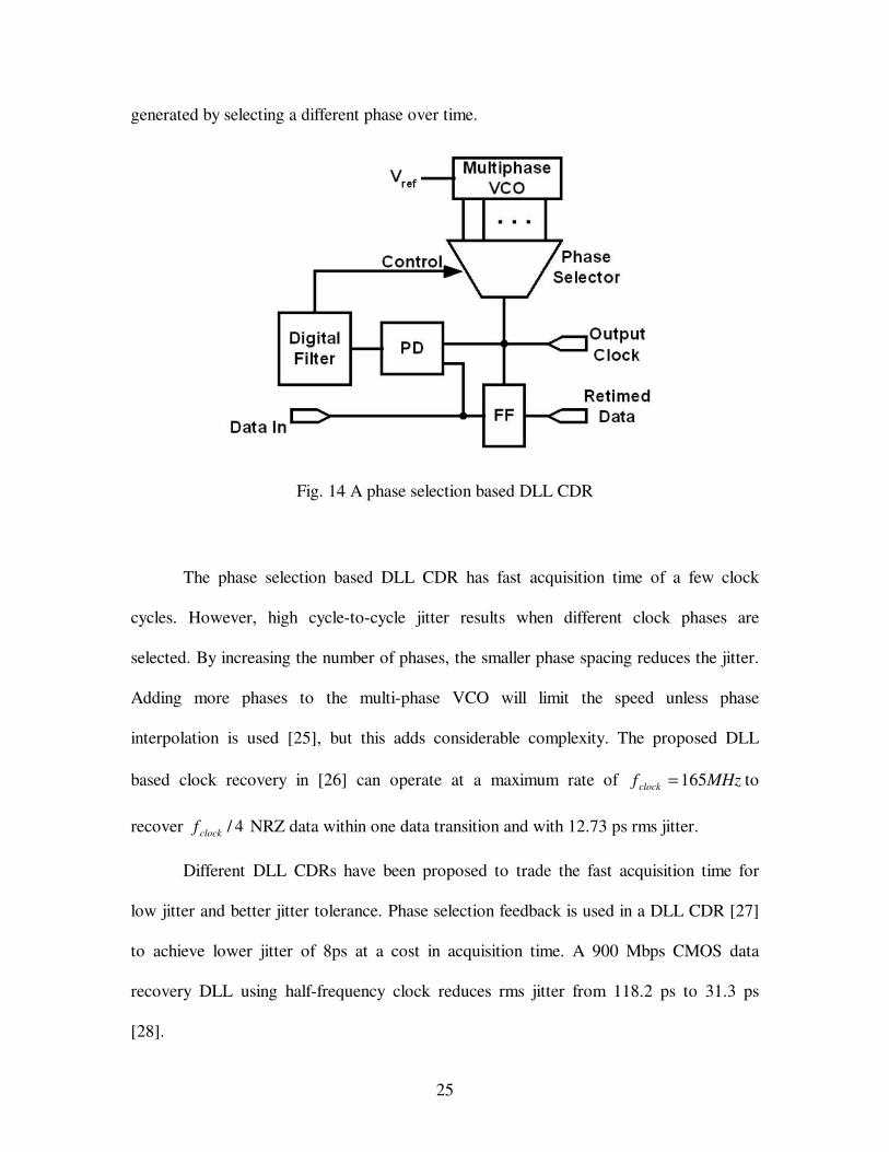
A block diagram of a phase selection based DLL CDR [24] is shown in Fig. 14.
The data are retimed with a flip-flop (FF) in the DLL. The multiphase VCO generates a
number of equally spaced clock phases at a frequency close to the data rate. The DLL
CDR generates the recovered clock by selecting the clock phase from the multiphase
VCO that is best aligned with the incoming data. If there is a certain frequency difference
between the VCO frequency and the incoming data, an appropriate clock can still be
P
P
sCI
π2
φin +
-
φout
KVCDL
25
generated by selecting a different phase over time.
Fig. 14 A phase selection based DLL CDR
The phase selection based DLL CDR has fast acquisition time of a few clock
cycles. However, high cycle-to-cycle jitter results when different clock phases are
selected. By increasing the number of phases, the smaller phase spacing reduces the jitter.
Adding more phases to the multi-phase VCO will limit the speed unless phase
interpolation is used [25], but this adds considerable complexity. The proposed DLL
based clock recovery in [26] can operate at a maximum rate of MHzf clock 165= to
recover 4/clockf NRZ data within one data transition and with 12.73 ps rms jitter.
Different DLL CDRs have been proposed to trade the fast acquisition time for
low jitter and better jitter tolerance. Phase selection feedback is used in a DLL CDR [27]
to achieve lower jitter of 8ps at a cost in acquisition time. A 900 Mbps CMOS data
recovery DLL using half-frequency clock reduces rms jitter from 118.2 ps to 31.3 ps
[28].
26
Other DLLs use phase mixers, phase selection, phase interpolation or self-biased
technique to achieve low jitter but long acquisition time [29]-[32]. Although a DLL in
[33] achieves both low jitter of 16ps and fast locking of 2 cycles using measure and
control scheme, the input of all these DLLs is a clock instead of NRZ random data.
Furthermore, DLLs generally require a reference clock while PLLs synthesize an in-
phase frequency equal to that of the data.
2.3 Combined delay and phase locked loop CDR
PLL solutions to CDRs usually use narrow-band loop filters to reduce jitter which
results in longer acquisition time. Although many PLL CDRs utilize techniques such as
PFD and PLL time-constant gear shifting to achieve fast acquisition at the start of the
incoming data, these techniques are limited since the PLL evaluates the frequency
difference between the reference and the generated clocks by means of the phase
difference. DLL CDRs can lock to the data in just a few clock cycles by means of phase
selection but have high jitter that results in higher BER performance. Therefore,
combined CDRs have been proposed.
Fig. 15 shows the hybrid CDR presented in [34] which uses a PLL locked into an
external reference clock to generate multiple clocks for a 1 GHz effective sampling rate,
and a DLL based on the location of detected transitions to process edge detection,
acquisition, tracking and programming, and achieves rms jitter of 100 ps, including the
input jitter, at a maximum data rate of 33 MHz and instant phase acquisition because of
the zero phase start algorithm. The frequency acquisition range of the hybrid CDR is very
limited.
27
Fig. 15 Hybrid CDR
Fig. 16 Block diagram of DLL/PLL CDR
PFD/CP
LPF
16-stage Differential Ring Oscillator
Parallel Phase Sampler
Parallel Register
DLL
Data In
Ref Clk
0° 22.5° (32 Taps)
Clock Data
PLL
Retiming Modules
VCPS
Data In
Retimed Data
Recovered Clock
PLL
VCXO (External)
Phase Detector
Loop Filter
DLL
28
The combined DLL/PLL CDR in [35] does not require an external frequency
reference. As shown in Fig. 16, the combined CDR contains two parallel loops. The
phase detector, loop filter, and VCXO (external voltage controlled crystal oscillator) form
the core of a PLL while the phase detector, loop filter, and VCPS (voltage controlled
phase shifter) form the core of a DLL. The two loops in the DLL/PLL act in concert to
reduce phase error to zero as follows: if the clock lags the data, the phase detector drives
the VCXO to a higher frequency and simultaneously increases the delay through the
VCPS. Both of these actions serve to reduce the initial phase error since the faster clock
picks up phase, while the delayed data lose phase. Finally, the initial phase error is
reduced to zero.
The DLL/PLL realizes rapid acquisition without compromising jitter filtering.
While phase errors are nulled out as fast as the DLL bandwidth φKK D ( DK and φK are
the gain constants of phase detector and VCPS) if the frequency of the DLL/PLL’s
VCXO equals to the incoming data rate, the jitter transfer function’s bandwidth is mainly
controlled by the low frequency pole at φKKVCXO / ( VCXOK is the gain constant of
VCXO). Increasing the DLL loop bandwidth by increasing DK makes the DLL acquire
more quickly, but does not diminish the DLL/PLL’s ability to filter jitter. However, fast
acquisition to a large frequency error cannot be achieved.
2.4 Combined CDR with fast acquisition and low jitter
Our approach to a fast acquisition CDR circuit with low jitter consists of a phase
selector, which can lock to the data in just a few clock cycles but has high jitter,
combined with a PLL, which requires a much longer acquisition time but provides a low-
29
jitter clock after it does lock. A novel phase frequency magnitude detection circuit is also
introduced to substantially reduce the PLL acquisition time.
30
CHAPTER THREE
COMBINED CDR WITH FAST ACQUISITION AND LOW JITTER
A combined phase selector/PLL CDR implemented in 0.5 µm CMOS from IBM
5HP BiCMOS process is presented in this dissertation to achieve both fast acquisition
time and low jitter [43]-[44].
Fig. 17 Combined PS/PLL CDR
A block diagram of the combined PS/PLL CDR is shown in Fig. 17. The phase
selector in Loop A can lock to the data with fast acquisition time of a few clock cycles.
The rate at which phase switching occurs decreases as the VCO approaches lock. Low
jitter is achieved after the PLL in Loop B acquires lock and phase switching is disabled.
Simulations in 0.5 µm CMOS technology show operation up to 800 Mbps, a 6%
acquisition range, an initial acquisition time of 8 bit times with 211 ps rms jitter, and jitter
of 7.5 ps after a PLL acquisition time of 650 ns. Feeding both the sign and magnitude of
the frequency difference between the input data and the VCO back to the phase detector

31
reduces the acquisition time substantially. It is called a phase frequency magnitude
detector. Simulations show that the 650 ns acquisition time is reduced by about a factor
of 4 to 150 ns from an initial 6% frequency difference.
3.1 Phase locked loop
Our conventional PLL design is shown in Fig. 18 and consists of a phase detector,
charge pump, low-pass filter and VCO with duty-cycle corrector. Note that an extra
capacitor 2C is added in parallel with PR and PC compared to the charge pump PLL in
Fig. 4. Since the charge pump drives the series combination of PR and PC , each time
current is injected into the loop filter, the control voltage experiences a large step. Even
in the locked condition, the mismatch between the currents of the charge pump and the
charge injection and clock feedthrough of the switches in the charge pump introduce
steps in the VCO control voltage. The resulting ripple severely disturbs the VCO,
corrupting the output phase. Therefore, a second capacitor is added to reduce this effect.
CPPD VCO Duty cyclecorrector
Vdd
CLKData
Cp
RpC2
Fig. 18 Phase locked loop
Phase detector
Because of the random nature of data there is not necessarily a data transition at
32
every clock cycle and the phase detector needs to handle sequences of consecutive zeros
and ones in the data stream. A half-rate phase detector is used in the PLL so that the VCO
can run at half the data rate. This relaxes the speed requirements. As an example, at an
800 Mbps data rate, the VCO operates at 400 MHz.
Din
Vout1 Vout2
CLK
Dout1
Dout2
D Q D Q
D Q D Q
A
B
C
DL2
L1 L3
L4
Fig. 19 Half-rate Phase detector
The Hogge topology is used in the half-rate phase detector, as shown in Fig. 19,
which uses both edges of the half-rate clock (CLK) to detect data transitions in the full-
rate random data (Din) [36]. Let CLKT be the period of the CLK. Assuming inD leads
CLK by T∆ , BAVout ⊕=1 exhibits a pulse of width T∆ for each data transition, and
DCVout ⊕=2 contains a pulse width of 2/CLKT for each input data edge, serving as the
reference output to overcome the ambiguity caused by data transition density. The
difference between the two outputs represents the phase error for data transitions. Under
33
locked condition, the proportional pulses are 4/CLKT wide, whereas the reference pulses
are 2/CLKT wide. The disparity between the average values of these outputs is removed
by halving the corresponding current source in the charge pump.
The Hoggy topology is a linear PD, generating a small average as the phase error
approaches zero. Thus, a charge pump driven by a Hogge PD experiences little “activity”
when the CDR is locked.
Charge pump
UP_PD
DOWN_PD
ICTRL
Fig. 20 Charge pump
The output pulses of the PD drive the current mirror of a charge pump [4], as
shown in Fig. 20, to assure the charge to the filter will not vary with the VCO control
voltage. Decreasing the current level of the charge pump reduces the ripple on the VCO
34
control voltage and hence the jitter but at the expense of acquisition time and range. A
larger current is initially used to achieve acquisition with larger loop bandwidth and then
the charge pump can be switched to a smaller current to reduce the jitter after lock is
achieved. The smaller current also allows a smaller implementation of the filter capacitor
on the chip.
VCO with duty-cycle corrector [23]
Vcon
D D
O O
D
D
O
O
D
D
O
O
D
D
O
O
O
O
D
D
M1 M2
M3 M4
M5 M6
Fig. 21 VCO
The VCO shown in Fig. 21 has four stages and generates multiple equal-spaced
phases of the clock for the phase selector. The basic differential delay cell consists of six
transistors. The transistors, M1 – M4, constitute a CMOS latch. The PMOS transistors at
the top, M5 and M6, control the oscillation frequency. When the VCO control voltage
Vcon is low, the driving currents of M5 and M6 increase. Therefore, the state of the latch
is changed easily and the delay time is reduced. The differential delay cell enables the
35
oscillator to be implemented with an even number of stages with the last stage outputs
crossed and connected to the first stage input. Four delay cells are used in the VCO to
generate the 8 clock phases required by the phase selector.
The advantage of a differential delay cell is lower susceptibility to power supply
noise because the inherent differential structure rejects the power supply noise. A tail
current source MOS transistor, which is commonly used in a differential CMOS pair, is
avoided to reduce 1/f noise. The latch sharpens the edge of the output signal so that the
added noise has little chance to be converted to jitter. Since the delay cell is basically a
simple differential inverter, a full-swing waveform is generated without additional level
shifters.
O
O
CLK (Duty corrected)
M1 M2
M3 M4
A
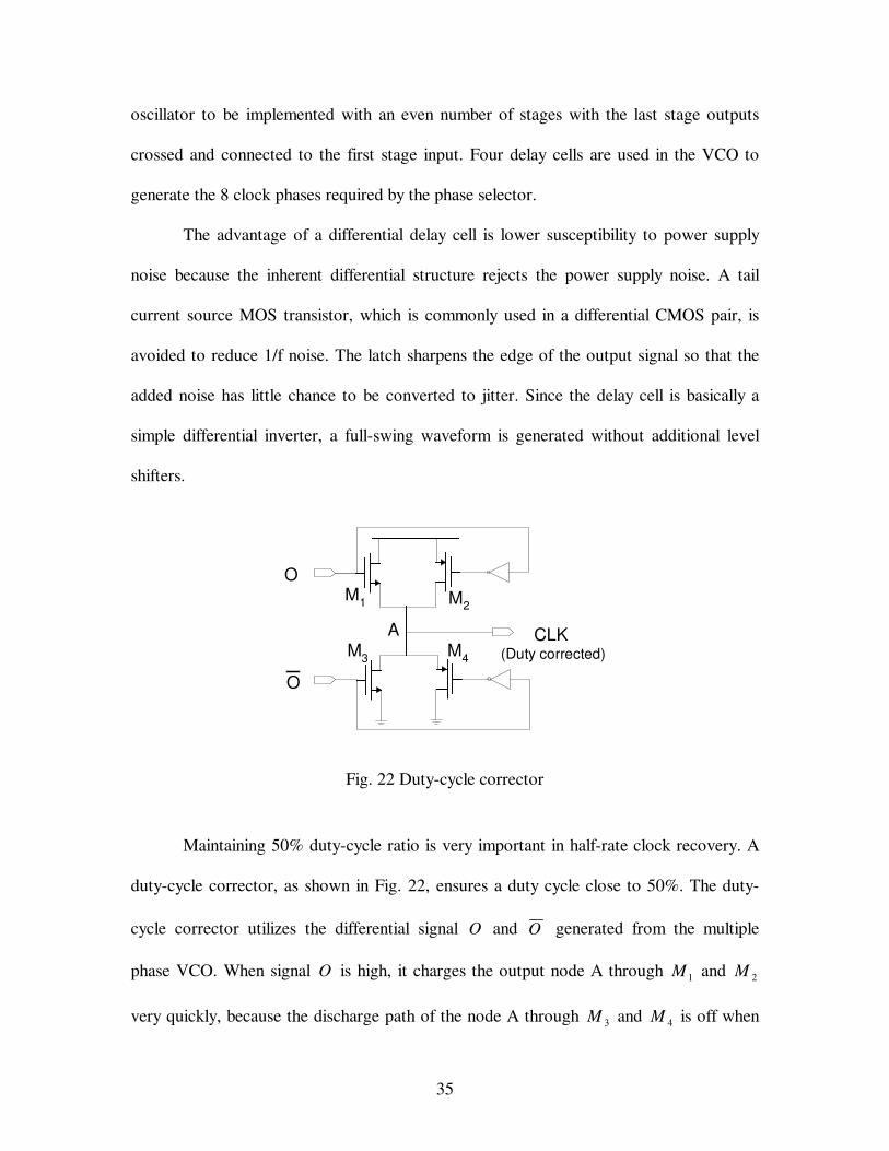
Fig. 22 Duty-cycle corrector
Maintaining 50% duty-cycle ratio is very important in half-rate clock recovery. A
duty-cycle corrector, as shown in Fig. 22, ensures a duty cycle close to 50%. The duty-
cycle corrector utilizes the differential signal O and O generated from the multiple
phase VCO. When signal O is high, it charges the output node A through 1M and 2M
very quickly, because the discharge path of the node A through 3M and 4M is off when
36
signal O is low. Similarly, when signal O is high, it rapidly discharges the node A with
the charge path off. Therefore, the rising edge and falling edge of the output signal CLK
are aligned with rising edges of signal O and O respectively. Since the rising edge of the
signal O is shifted by °180 in phase from that of O , the duty-cycle corrector delivers
50% duty-cycle signal CLK. The output signal CLK is generated by exchanging the
input signals of O and O . Eight duty-cycle correctors are used for the eight clock phases
from the VCO.
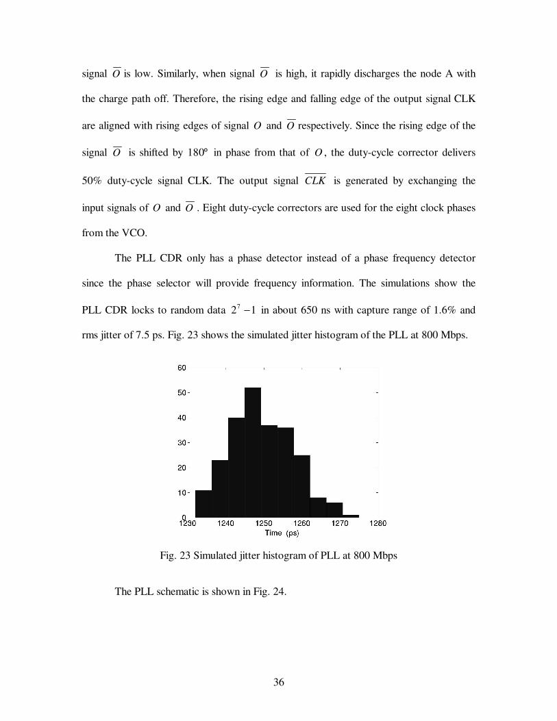
The PLL CDR only has a phase detector instead of a phase frequency detector
since the phase selector will provide frequency information. The simulations show the
PLL CDR locks to random data 127 − in about 650 ns with capture range of 1.6% and
rms jitter of 7.5 ps. Fig. 23 shows the simulated jitter histogram of the PLL at 800 Mbps.
Fig. 23 Simulated jitter histogram of PLL at 800 Mbps
The PLL schematic is shown in Fig. 24.

37
Fig.
24
PL
L s
chem
atic

38
3.2 Phase Selector
The phase selector takes multiple delayed versions of the local clock, generated
by the multiple-phase VCO in the PLL, and continuously examines the relationship
between transitions in the data and transitions of these clock phases. The circuit then
selects the clock phase, which is farthest from the data transitions, to sample the data. In
the example shown in Fig. 25 with four clock phases, clock CLK2 or CLK3 should be
used to latch the data. Clocks CLK1 and CLK4 have transitions close to data transitions
and selecting either of these might lead to setup and hold violations of the data latch
causing a higher number of bit errors. It is assumed here that the data is eventually
latched with both the rising and falling edges.
D A T A
C L K 1
C L K 2
C L K 3
C L K 4
Fig. 25 Multiple clock phases versus data
Because the data and the local clock are not at the same frequency, the circuit will
either be advancing or retarding the phase selection in order to acquire the data correctly.
The circuit should take into account the direction of the phase drift in order to make the
best clock phase selection, which has a transition farthest from the data transitions.
39
Fig.
26
Phas
e se
lect
or b
lock
dia
gram
Inpu
t sec
tion
sam
ples
and
al
igns
dat
a
Det
erm
ines
re
lativ
e ph
ase
diff
eren
ce
Phas
e st
ate
latc
hes
Stat
e lo
gic
Mul
tiple
xer
40
In over-sampling clock recovery methods the usual over-sampling rate is 8 to 16
times the frequency. In order to handle this higher frequency clock, a higher performance
technology would be required. With the phase selector, a higher frequency clock is not
required and the same technology that is used to generate the data can be used to recover
the clock. This is especially important at GHz clock rates where technologies that can
clock at higher frequency are limited and expensive.
The implementation of the phase selector, Loop A in Fig.16, with 4 phases per bit
is shown in Fig. 26. The input section samples and aligns the incoming data with eight
equally-spaced clock phases obtained from the VCO, and generates data transition
information. Four phase states (X1 to X4) are then obtained from the relative phase
difference between the data transitions and clock phases. The state logic determines the
clock phase farthest from the data transitions and controls the multiplexer to output the
clock. Since the phase selector relies on the sampling of the incoming data, the problem
of metastability in the data latches must be considered. Eight data paths use multiple
latches to reduce the probability of a metastability-induced data error. The final latch
stages of all 8 data paths are clocked by the same clock for further processing.
Simulations show phase selector operation up to 800 Mbps. As shown in the
timing diagram obtained from the simulation of the phase selector in Fig. 27, the four
phase states generated by the phase selector select the most appropriate phase from the
multiple clock phases based on the relationship of the data transitions and the clock
phases. The selection process causes high cycle-to-cycle jitter as different clock phases
are selected. Note in the clock output (CLKOUT) when a state change occurs in Fig. 27
the slightly larger pulse widths if the data is slower and the slightly smaller pulse widths
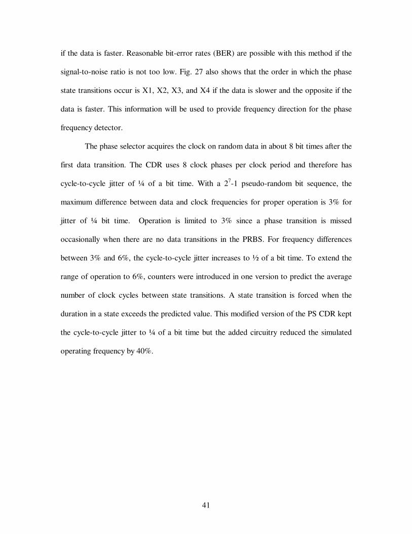
41
if the data is faster. Reasonable bit-error rates (BER) are possible with this method if the
signal-to-noise ratio is not too low. Fig. 27 also shows that the order in which the phase
state transitions occur is X1, X2, X3, and X4 if the data is slower and the opposite if the
data is faster. This information will be used to provide frequency direction for the phase
frequency detector.
The phase selector acquires the clock on random data in about 8 bit times after the
first data transition. The CDR uses 8 clock phases per clock period and therefore has
cycle-to-cycle jitter of ¼ of a bit time. With a 27-1 pseudo-random bit sequence, the
maximum difference between data and clock frequencies for proper operation is 3% for
jitter of ¼ bit time. Operation is limited to 3% since a phase transition is missed
occasionally when there are no data transitions in the PRBS. For frequency differences
between 3% and 6%, the cycle-to-cycle jitter increases to ½ of a bit time. To extend the
range of operation to 6%, counters were introduced in one version to predict the average
number of clock cycles between state transitions. A state transition is forced when the
duration in a state exceeds the predicted value. This modified version of the PS CDR kept
the cycle-to-cycle jitter to ¼ of a bit time but the added circuitry reduced the simulated
operating frequency by 40%.
42
(a) Data slower than clock
X1
X2
X3
X4
DATA
CLKOUT
CLK1
CLK2
CLK3
CLK4
X1
X2
X3
X4
DATA
CLKOUT
CLK1
CLK2
CLK3
CLK4
(b) Data faster than clock
Fig. 27 Operation of phase selector
43
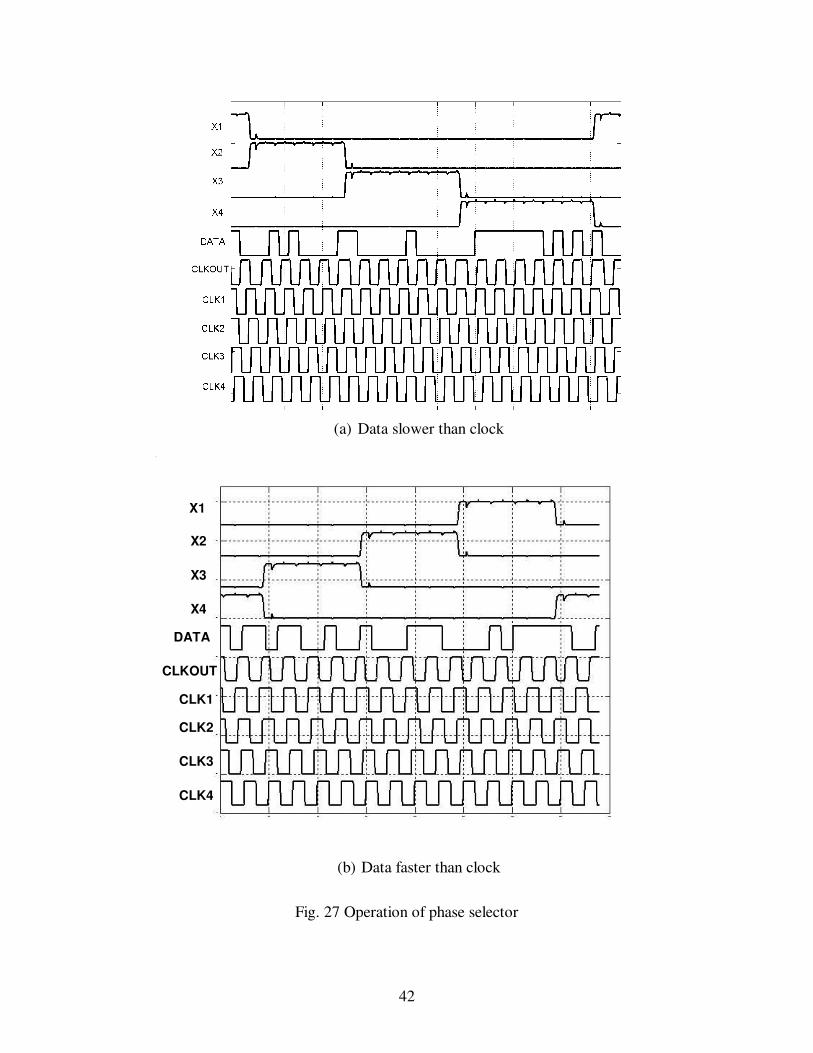
3.3 Combined CDR with PFD
The phase detector has only a limited capture range since a large difference in
frequency between the VCO and the incoming data has a zero average phase difference.
The addition of the frequency detector can extend this range considerably. Two versions
of CDR were designed which combine the 3% version of the phase selector and the phase
locked loop. In the first version, only the sign of the frequency offset is fed to the phase
detector, converting the phase detector into a phase frequency detector. The sign of the
frequency difference can be determined with little additional logic in the phase selector
from the order in which the phase-state transitions occur.
UP_FD
DOWN_FD
ICTRL
Fig. 28 Charge pump for frequency detection
44
A second charge pump that is the same architecture as the PLL charge pump is
added to provide frequency detection feedback to the VCO control voltage, as shown in
Fig. 28. The up_fd and down_fd signals, which provide frequency direction, are obtained
in the phase selector from the order in which the phase-state transitions occur. The timing
diagrams of the phase selector in Fig. 27 show that the order of the phase states is X1,
X2, X3 and X4 when data is slower than the clock. For the case when data is faster, the
order of the phase states is X4, X3, X2 and X1. The up and down signals control the
charge pump to generate the current pulses of small value which are applied to the VCO
control voltage to drive the clock frequency gradually to the data rate. If these current
pulses are too large, the VCO frequency may not settle in the capture range of the PLL.
The waveforms from the simulation of combined CDR with PFD are shown in
Fig. 29. The pulses in up_fd and down_fd provide frequency direction and control the
charge pump to generate the small current pulses corresponding to frequency direction.
These current pulses charge or discharge the capacitor of the loop filter to accordingly
change the VCO control voltage (Cont). Frequency feedback is turned off when the
frequency difference reduces to 0.5%, well within the range of the PD. Finally, the PLL
acquires lock with low jitter of 7.5 ps. The frequency detector does not contribute any
jitter to the recovered clock.
Simulations show operation up to 800 Mbps, a 6% acquisition range, an
acquisition time of 8 bit times with initial rms jitter of 211 ps and after about 650 ns, the
jitter reduces to 7.5 ps. Compared to the PLL alone, the capture range increases from
1.6% to 6%. The acquisition time from 6% is about the same as that of the PLL alone
starting with a frequency difference of only 1.6%. The acquisition times are shown in
45
Fig. 30, which shows the VCO control voltages for the PLL CDR and the combined
phase selector/PLL CDR.
(a) Data slower than clock
(b)Data faster than clock
Fig. 29 Waveforms from combined CDR with PFD
Up
Cont
Ictrl
Down
UP
Cont
Ictrl
Down
46
Fig. 30 Comparison of acquisition time
3.4 Combined CDR with PFMD
In the second version of the combined CDR, we add a novel phase frequency
magnitude detector to substantially reduce the acquisition time by feeding back the
frequency magnitude to the charge pump as well as direction.
In addition to the sign of the frequency difference, the phase selector can also
provide an estimate of the magnitude of the frequency that is inversely proportional to the
counter number of VCO clock cycles for a 1/2 bit-time phase shift with respect to the
incoming data. Using this additional information the acquisition time can be reduced
considerably by applying a single current pulse of the proper magnitude to the VCO
control voltage to quickly change it to the desired value. The required current pulse
magnitude to achieve short acquisition time was found to be inversely proportional to the
47
count of VCO clock cycles contained in the counter. The relationship among the
magnitude of frequency offset, the count number of VCO clock cycles for a 1/2 bit-time
phase shift with respect to the incoming data, and the magnitude of the current pulse
required for fast acquisition is shown in Table 1.
Table 1 Counter number, magnitude of current pulse versus frequency offset
2.5mA46%
2.1mA55%
1.7mA64%
1.2mA83%
0.8mA132%
0.4mA251%
Magnitude of current pulse
Counter Number
Magnitude of frequency offset
2.5mA46%
2.1mA55%
1.7mA64%
1.2mA83%
0.8mA132%
0.4mA251%
Magnitude of current pulse
Counter Number
Magnitude of frequency offset
The count from the phase selector is input to a look-up table, implemented with
the digital logic shown in Fig. 31, to convert the count, i4 – i0, into a 5-bit current
magnitude, o4 – o0. This is input to a third combined charge pump shown in Fig. 32,
consisting of 5 single charge pumps that generate binary weighted currents. Thus, o4 – o0
determine the current magnitude of this charge pump. The single up or down pulse
controls this charge pump to generate a single current pulse of the proper magnitude for
fast acquisition of the PLL. The up or down pulse is generated by the digital logic right
after a ½ bit time shift in the VCO phase with respect to the incoming data. Two clock
cycles are allowed for logic delay and settling of the charge pump current. The single
current pulse quickly drives the VCO frequency to the data rate.
48
‘1’
‘1’
‘1’
‘0’ ‘0’
‘0’
‘0’
i0
i1
i2
i3i4
o0
o1
o2
o3
o4
b4
b3
b2
b1
b0
2-4 Decoder
4X5 R
OM
Fig. 31 Digital logic implementation of the look-up table
UP
DOWN
O0 O1 O2 O3 O4
X1 X2 X4 X8 X16ICTRL
Fig. 32 PFMD charge pump

49
(a) Data faster than clock
(b) Data faster than clock
Fig. 33 Waveforms from the PFMD simulation
UP
Cont
Ictrl
Down
UP
Cont
Ictrl
Down

50
The waveforms from the simulation of the combined CDR with PFMD are shown
in Fig. 33. The single up or down pulse control the 5 charge pumps to provide an
appropriate current pulse. This single pulse is applied to the VCO control voltage to
quickly change it to the desired value.
Simulations show that the 650 ns acquisition time can be reduced to less than 200
ns with this approach. Fig. 34 shows the VCO control voltages of the combined CDR
with and without frequency magnitude feedback for an initial frequency offset between
the VCO and the input data of 6%.
Fig. 34 Acquisition time of combined CDR with PFMD and with PFD
The chip layout is shown in Fig. 35, containing the analog PLL circuit and the
digital phase selector circuit. Because this CDR circuit is a mixed-signal integrated
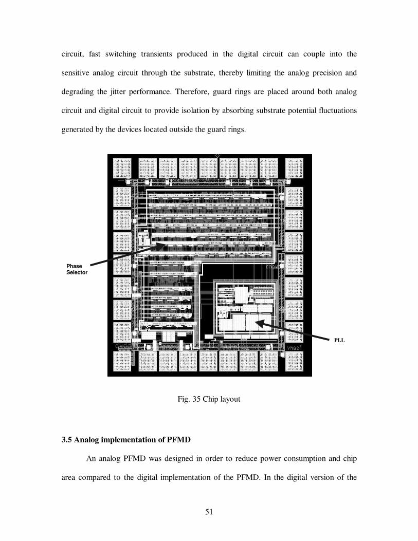
51
circuit, fast switching transients produced in the digital circuit can couple into the
sensitive analog circuit through the substrate, thereby limiting the analog precision and
degrading the jitter performance. Therefore, guard rings are placed around both analog
circuit and digital circuit to provide isolation by absorbing substrate potential fluctuations
generated by the devices located outside the guard rings.
Fig. 35 Chip layout
3.5 Analog implementation of PFMD
An analog PFMD was designed in order to reduce power consumption and chip
area compared to the digital implementation of the PFMD. In the digital version of the
PLL
Phase Selector
52
PFMD CDR, counters in the phase selector are used to measure the time it takes that
different phase changes occur and a look-up table is implemented to convert the time to
frequency difference between clock and incoming data. In the analog implementation of
the PFMD CDR, the phase selector is eliminated so that the CDR does not acquire lock
within a few clock cycles. However, the PLL’s fast locking of less than 200 ns in the
analog PFMD CDR is still an advantage in many applications.
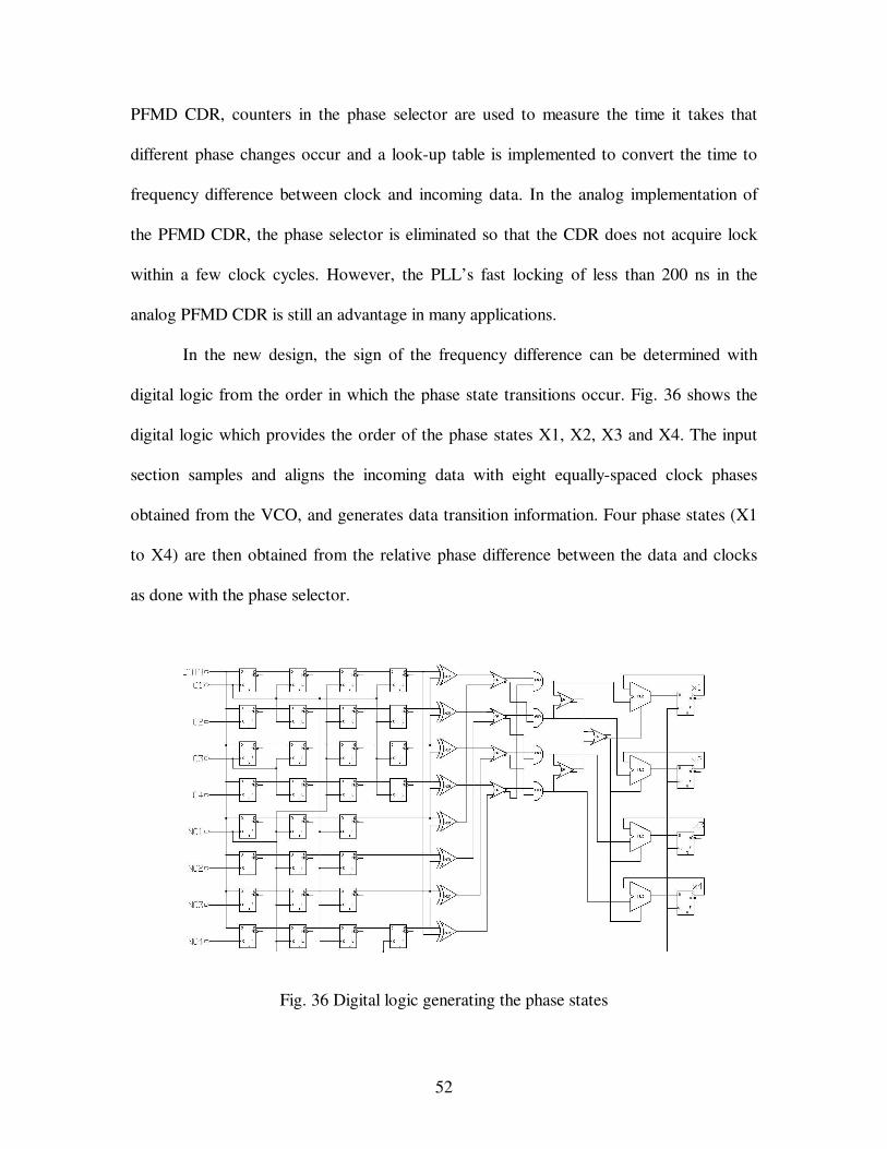
In the new design, the sign of the frequency difference can be determined with
digital logic from the order in which the phase state transitions occur. Fig. 36 shows the
digital logic which provides the order of the phase states X1, X2, X3 and X4. The input
section samples and aligns the incoming data with eight equally-spaced clock phases
obtained from the VCO, and generates data transition information. Four phase states (X1
to X4) are then obtained from the relative phase difference between the data and clocks
as done with the phase selector.
Fig. 36 Digital logic generating the phase states

53
An RC filter, as shown in Fig. 37, is used to obtain a voltage proportional to the
time it takes to transition between different phases. Thus, in addition to the sign of the
frequency difference, the analog PFMD provides the estimate of the magnitude of
frequency difference by using the RC filter instead of a lookup table to perform the
inversion from time to frequency difference.
Fig. 37 Analog PFMD
The waveforms from the simulation of the analog PFMD CDR are shown in Fig.
38. Only one up or down pulse is generated by the digital logic when the VCO shifts in
phase with respect to the incoming data by ½ bit time. Input to the analog PFMD (In) is a
negative digital pulse with width equal to the time the VCO shifts in phase by 1 bit time
with respect to the input data. Then the RC filter is used to generate the bias voltages Vb2
and Vb1 that control the magnitude of current in the PFMD charge pump. The magnitude
In Vb2
Vb1
Vp To charge pump
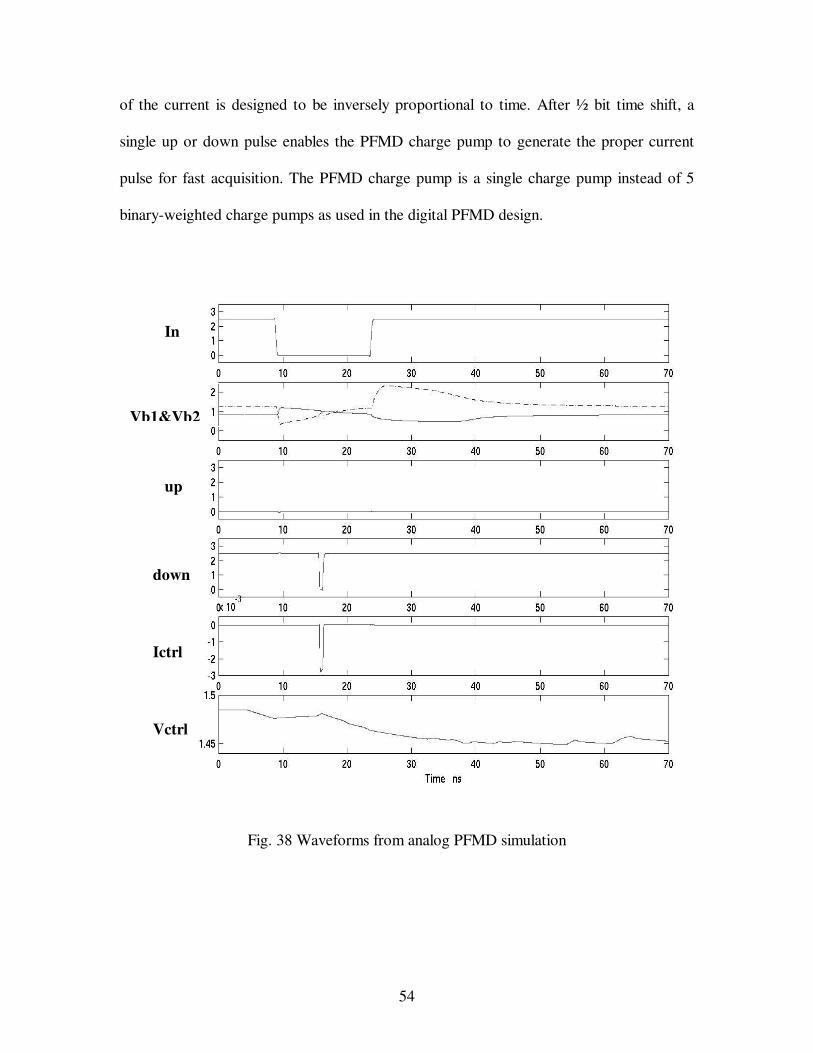
54
of the current is designed to be inversely proportional to time. After ½ bit time shift, a
single up or down pulse enables the PFMD charge pump to generate the proper current
pulse for fast acquisition. The PFMD charge pump is a single charge pump instead of 5
binary-weighted charge pumps as used in the digital PFMD design.
Fig. 38 Waveforms from analog PFMD simulation
In
Vb1&Vb2
up
down
Ictrl
Vctrl
55
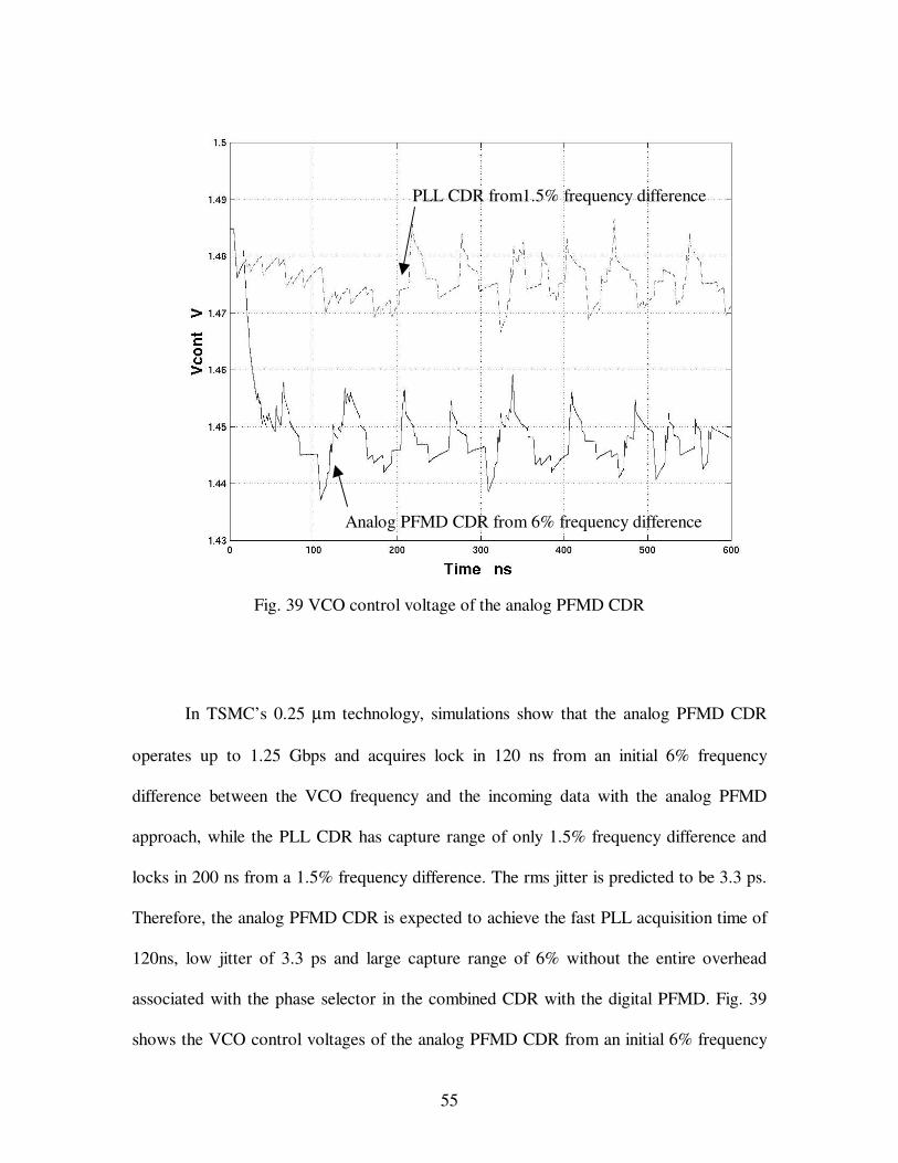
Fig. 39 VCO control voltage of the analog PFMD CDR
In TSMC’s 0.25 µm technology, simulations show that the analog PFMD CDR
operates up to 1.25 Gbps and acquires lock in 120 ns from an initial 6% frequency
difference between the VCO frequency and the incoming data with the analog PFMD
approach, while the PLL CDR has capture range of only 1.5% frequency difference and
locks in 200 ns from a 1.5% frequency difference. The rms jitter is predicted to be 3.3 ps.
Therefore, the analog PFMD CDR is expected to achieve the fast PLL acquisition time of
120ns, low jitter of 3.3 ps and large capture range of 6% without the entire overhead
associated with the phase selector in the combined CDR with the digital PFMD. Fig. 39
shows the VCO control voltages of the analog PFMD CDR from an initial 6% frequency
PLL CDR from1.5% frequency difference
Analog PFMD CDR from 6% frequency difference
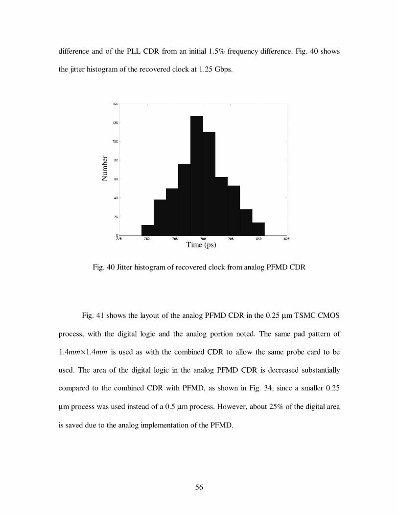
56
difference and of the PLL CDR from an initial 1.5% frequency difference. Fig. 40 shows
the jitter histogram of the recovered clock at 1.25 Gbps.
Fig. 40 Jitter histogram of recovered clock from analog PFMD CDR
Fig. 41 shows the layout of the analog PFMD CDR in the 0.25 µm TSMC CMOS
process, with the digital logic and the analog portion noted. The same pad pattern of
mmmm 4.14.1 × is used as with the combined CDR to allow the same probe card to be
used. The area of the digital logic in the analog PFMD CDR is decreased substantially
compared to the combined CDR with PFMD, as shown in Fig. 34, since a smaller 0.25
µm process was used instead of a 0.5 µm process. However, about 25% of the digital area
is saved due to the analog implementation of the PFMD.
Time (ps)
Num
ber
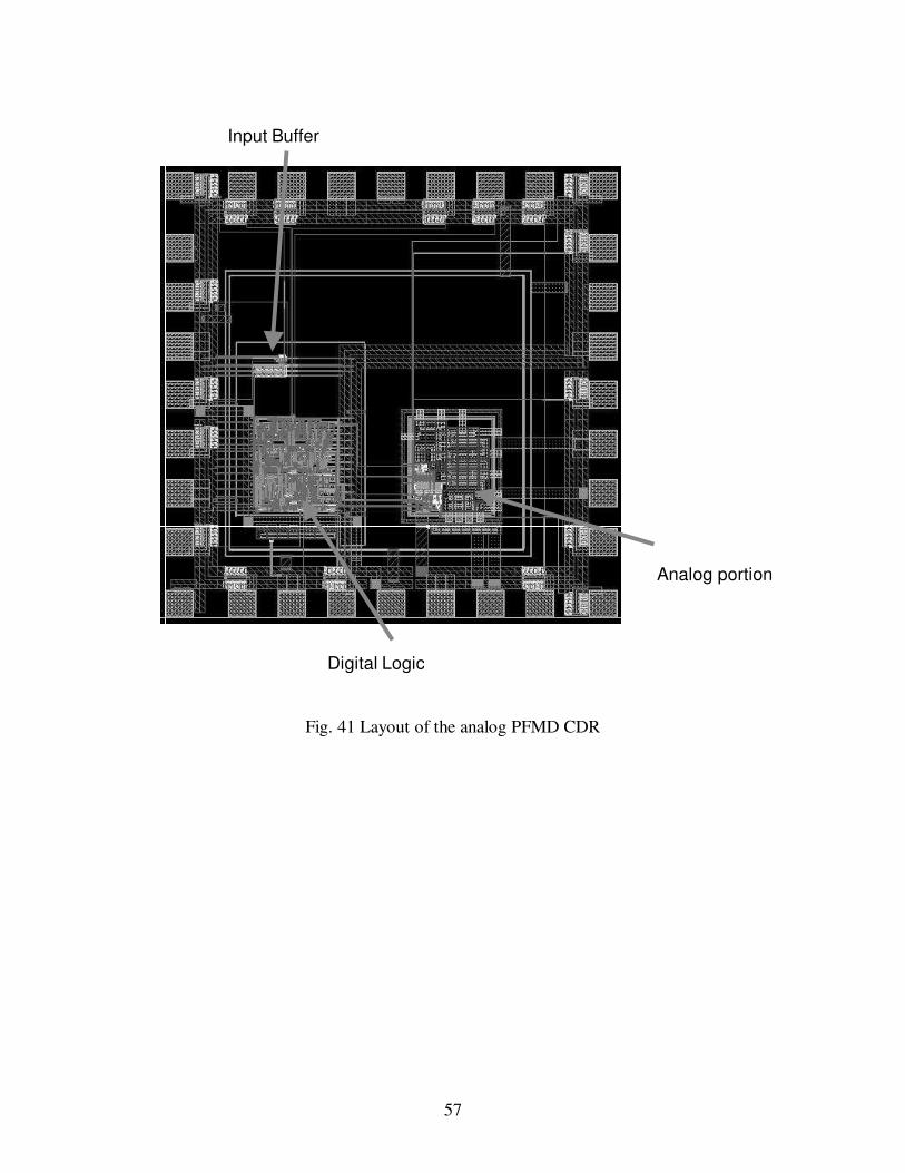
57
Fig. 41 Layout of the analog PFMD CDR
Analog portion
Digital Logic
Input Buffer
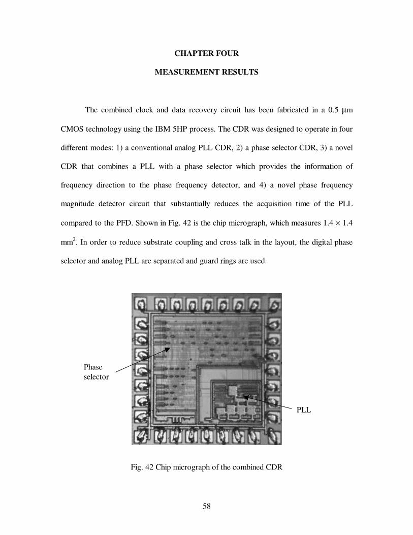
58
CHAPTER FOUR
MEASUREMENT RESULTS
The combined clock and data recovery circuit has been fabricated in a 0.5 µm
CMOS technology using the IBM 5HP process. The CDR was designed to operate in four
different modes: 1) a conventional analog PLL CDR, 2) a phase selector CDR, 3) a novel
CDR that combines a PLL with a phase selector which provides the information of
frequency direction to the phase frequency detector, and 4) a novel phase frequency
magnitude detector circuit that substantially reduces the acquisition time of the PLL
compared to the PFD. Shown in Fig. 42 is the chip micrograph, which measures 1.4 × 1.4
mm2. In order to reduce substrate coupling and cross talk in the layout, the digital phase
selector and analog PLL are separated and guard rings are used.
Fig. 42 Chip micrograph of the combined CDR
PLL
Phase selector

59
4.1 Measurement Methods
The combined CDR was tested at the wafer level up to 700 Mbps with 27-1 PRBS
data. High-speed inputs and outputs are contacted with 50Ω controlled impedance
ceramic probes connected to coaxial cables. The output waveforms and jitter were
observed with a sampling oscilloscope. The acquisition time was measured using a 4
GSps digital oscilloscope. Fig. 43 shows the probe station with the probe card and a
metal box that shields all the control signals. Fig. 44 shows the measurement setup
including the probe station, the sampling oscilloscope, the digital oscilloscope and the
pattern generator.
Fig. 43 The probe station
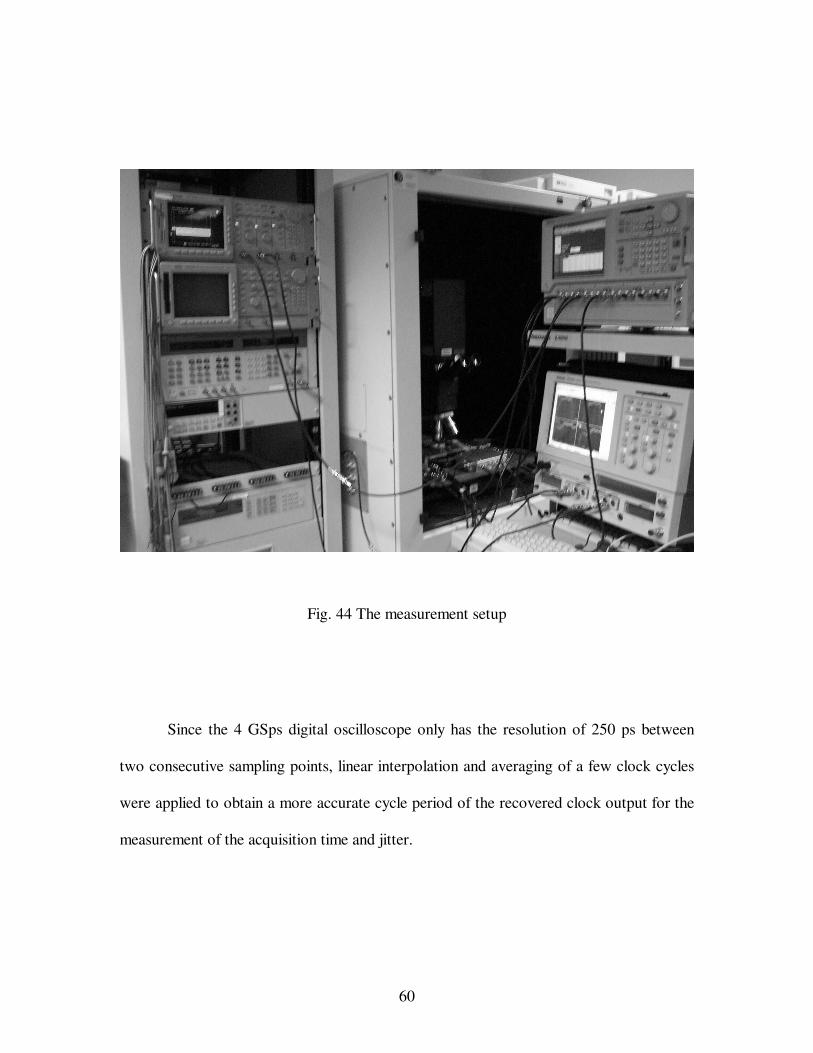
60
Fig. 44 The measurement setup
Since the 4 GSps digital oscilloscope only has the resolution of 250 ps between
two consecutive sampling points, linear interpolation and averaging of a few clock cycles
were applied to obtain a more accurate cycle period of the recovered clock output for the
measurement of the acquisition time and jitter.
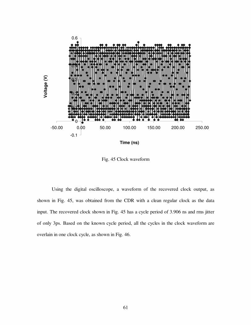
61
-0.1
0
0.1
0.2
0.3
0.4
0.5
0.6
-50.00 0.00 50.00 100.00 150.00 200.00 250.00
Time (ns)
Vol
tage
(V)
Fig. 45 Clock waveform
Using the digital oscilloscope, a waveform of the recovered clock output, as
shown in Fig. 45, was obtained from the CDR with a clean regular clock as the data
input. The recovered clock shown in Fig. 45 has a cycle period of 3.906 ns and rms jitter
of only 3ps. Based on the known cycle period, all the cycles in the clock waveform are
overlain in one clock cycle, as shown in Fig. 46.
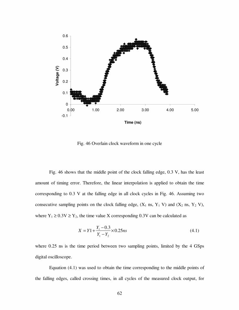
62
-0.1
0
0.1
0.2
0.3
0.4
0.5
0.6
0.00 1.00 2.00 3.00 4.00 5.00
Time (ns)
Vol
tage
(V)
Fig. 46 Overlain clock waveform in one cycle
Fig. 46 shows that the middle point of the clock falling edge, 0.3 V, has the least
amount of timing error. Therefore, the linear interpolation is applied to obtain the time
corresponding to 0.3 V at the falling edge in all clock cycles in Fig. 46. Assuming two
consecutive sampling points on the clock falling edge, (X1 ns, Y1 V) and (X2 ns, Y2 V),
where Y1 ≥ 0.3V ≥ Y2, the time value X corresponding 0.3V can be calculated as
nsYY
YYX 25.0
3.01
21
1 ×−−
+= (4.1)
where 0.25 ns is the time period between two sampling points, limited by the 4 GSps
digital oscilloscope.
Equation (4.1) was used to obtain the time corresponding to the middle points of
the falling edges, called crossing times, in all cycles of the measured clock output, for
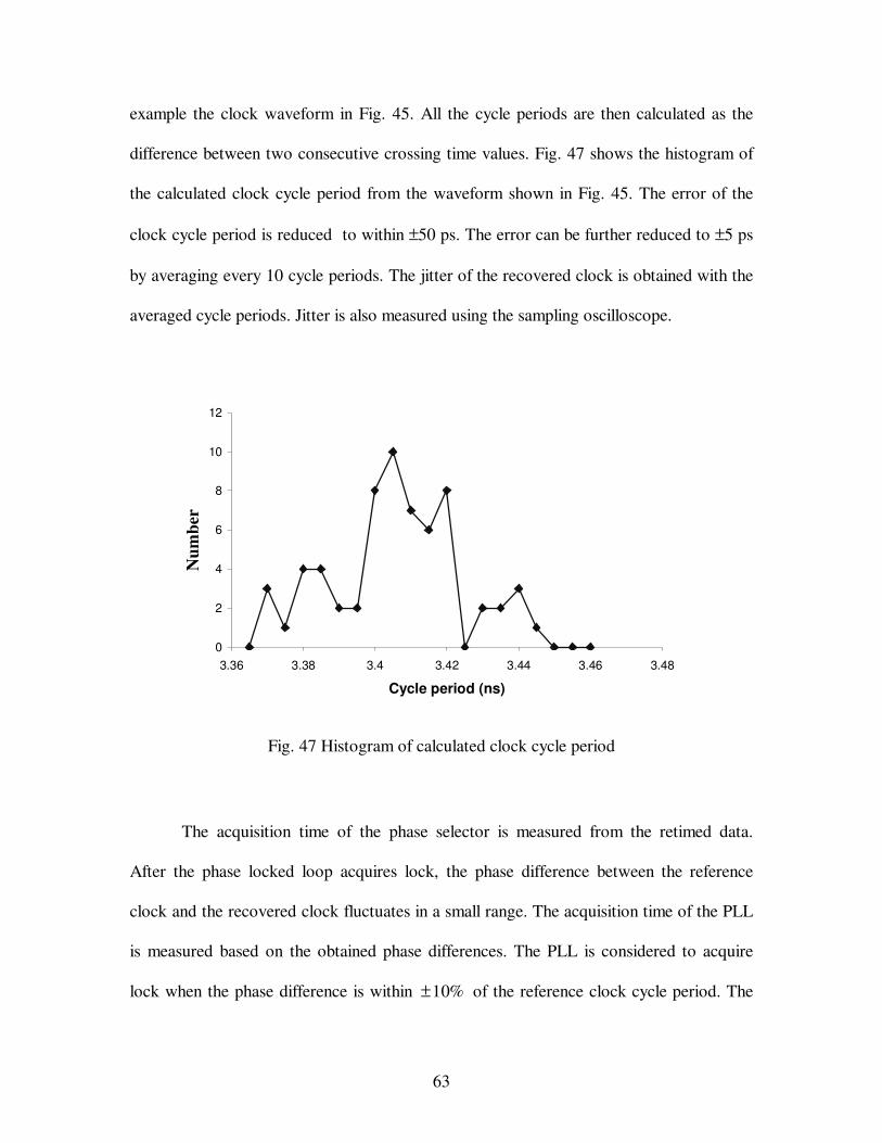
63
example the clock waveform in Fig. 45. All the cycle periods are then calculated as the
difference between two consecutive crossing time values. Fig. 47 shows the histogram of
the calculated clock cycle period from the waveform shown in Fig. 45. The error of the
clock cycle period is reduced to within ±50 ps. The error can be further reduced to ±5 ps
by averaging every 10 cycle periods. The jitter of the recovered clock is obtained with the
averaged cycle periods. Jitter is also measured using the sampling oscilloscope.
0
2
4
6
8
10
12
3.36 3.38 3.4 3.42 3.44 3.46 3.48
Cycle period (ns)
Fig. 47 Histogram of calculated clock cycle period
The acquisition time of the phase selector is measured from the retimed data.
After the phase locked loop acquires lock, the phase difference between the reference
clock and the recovered clock fluctuates in a small range. The acquisition time of the PLL
is measured based on the obtained phase differences. The PLL is considered to acquire
lock when the phase difference is within %10± of the reference clock cycle period. The
Num
ber
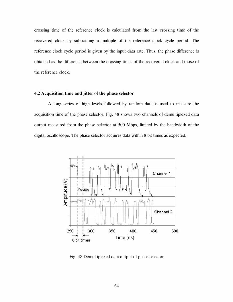
64
crossing time of the reference clock is calculated from the last crossing time of the
recovered clock by subtracting a multiple of the reference clock cycle period. The
reference clock cycle period is given by the input data rate. Thus, the phase difference is
obtained as the difference between the crossing times of the recovered clock and those of
the reference clock.
4.2 Acquisition time and jitter of the phase selector
A long series of high levels followed by random data is used to measure the
acquisition time of the phase selector. Fig. 48 shows two channels of demultiplexed data
output measured from the phase selector at 500 Mbps, limited by the bandwidth of the
digital oscilloscope. The phase selector acquires data within 8 bit times as expected.
Fig. 48 Demultiplexed data output of phase selector
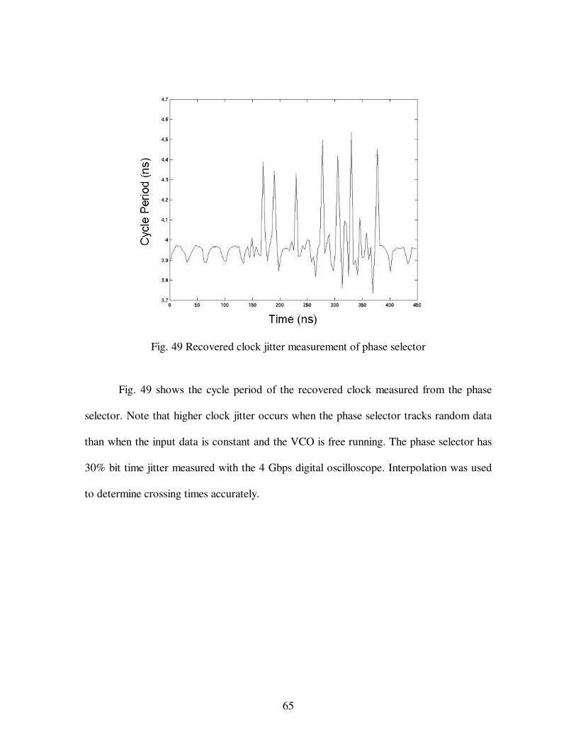
65
Fig. 49 Recovered clock jitter measurement of phase selector
Fig. 49 shows the cycle period of the recovered clock measured from the phase
selector. Note that higher clock jitter occurs when the phase selector tracks random data
than when the input data is constant and the VCO is free running. The phase selector has
30% bit time jitter measured with the 4 Gbps digital oscilloscope. Interpolation was used
to determine crossing times accurately.
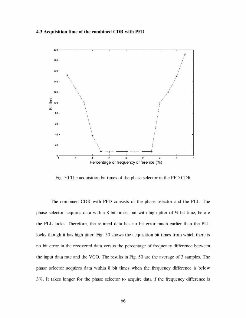
66
4.3 Acquisition time of the combined CDR with PFD
Fig. 50 The acquisition bit times of the phase selector in the PFD CDR
The combined CDR with PFD consists of the phase selector and the PLL. The
phase selector acquires data within 8 bit times, but with high jitter of ¼ bit time, before
the PLL locks. Therefore, the retimed data has no bit error much earlier than the PLL
locks though it has high jitter. Fig. 50 shows the acquisition bit times from which there is
no bit error in the recovered data versus the percentage of frequency difference between
the input data rate and the VCO. The results in Fig. 50 are the average of 3 samples. The
phase selector acquires data within 8 bit times when the frequency difference is below
3%. It takes longer for the phase selector to acquire data if the frequency difference is

67
larger than 3% because the recovered clock has higher jitter of half bit time. The
recovered data has no bit errors when the frequency difference reduces to less than 3%.
In the combined PFD CDR the sign of the frequency offset is fed to the phase
detector, essentially converting the phase detector into a phase frequency detector. Fig.
51 shows one sample of the cycle period of the recovered clock measured from the
combined PFD CDR with VCO initially at 600 Mbps and 27-1 PRBS data at 650 Mbps.
Fig. 52 shows one sample of the phase difference between the recovered clock and the
reference clock with the same conditions. Appendix A shows the cycle periods of the
recovered clock and the phase differences between the recovered clock and the reference
clock at different data rate from 555 Mbps to 650 Mbps with step size of 5 Mbps.
Fig. 51 Cycle period of the recovered clock from PFD CDR at data rate 650 Mbps
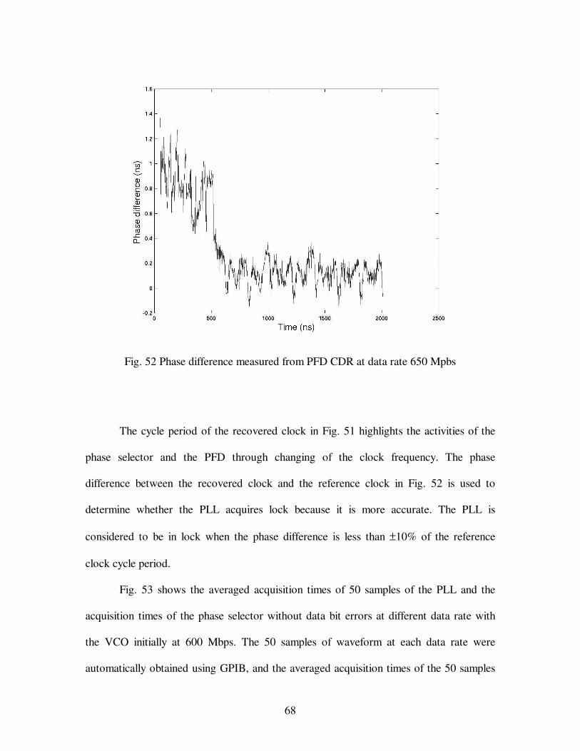
68
Fig. 52 Phase difference measured from PFD CDR at data rate 650 Mpbs
The cycle period of the recovered clock in Fig. 51 highlights the activities of the
phase selector and the PFD through changing of the clock frequency. The phase
difference between the recovered clock and the reference clock in Fig. 52 is used to
determine whether the PLL acquires lock because it is more accurate. The PLL is
considered to be in lock when the phase difference is less than ±10% of the reference
clock cycle period.
Fig. 53 shows the averaged acquisition times of 50 samples of the PLL and the
acquisition times of the phase selector without data bit errors at different data rate with
the VCO initially at 600 Mbps. The 50 samples of waveform at each data rate were
automatically obtained using GPIB, and the averaged acquisition times of the 50 samples
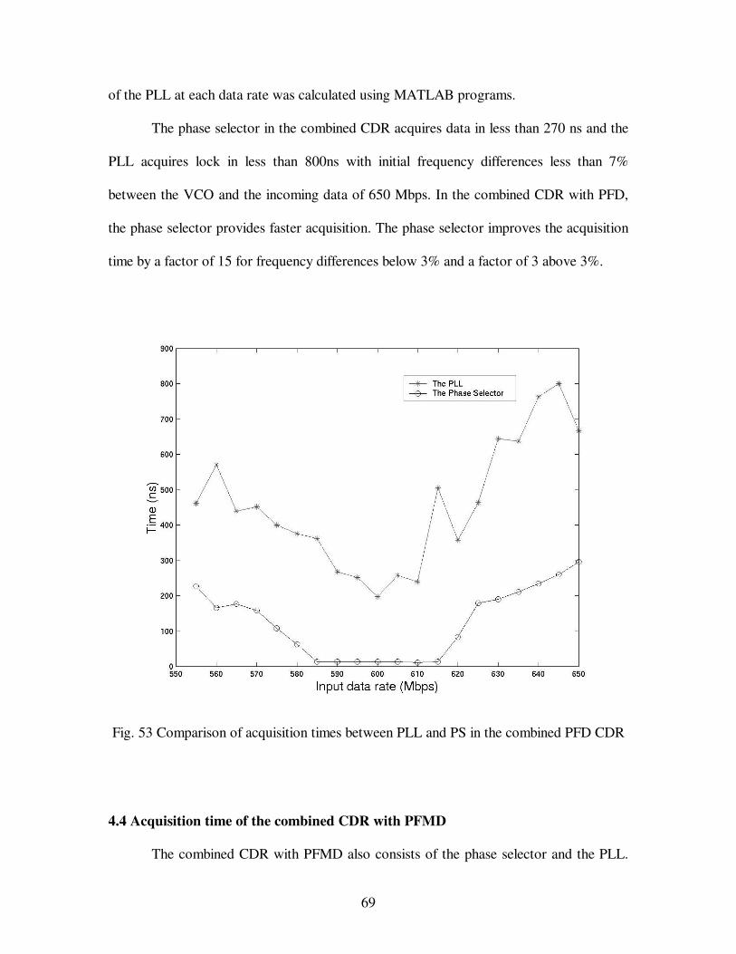
69
of the PLL at each data rate was calculated using MATLAB programs.
The phase selector in the combined CDR acquires data in less than 270 ns and the
PLL acquires lock in less than 800ns with initial frequency differences less than 7%
between the VCO and the incoming data of 650 Mbps. In the combined CDR with PFD,
the phase selector provides faster acquisition. The phase selector improves the acquisition
time by a factor of 15 for frequency differences below 3% and a factor of 3 above 3%.
Fig. 53 Comparison of acquisition times between PLL and PS in the combined PFD CDR
4.4 Acquisition time of the combined CDR with PFMD
The combined CDR with PFMD also consists of the phase selector and the PLL.
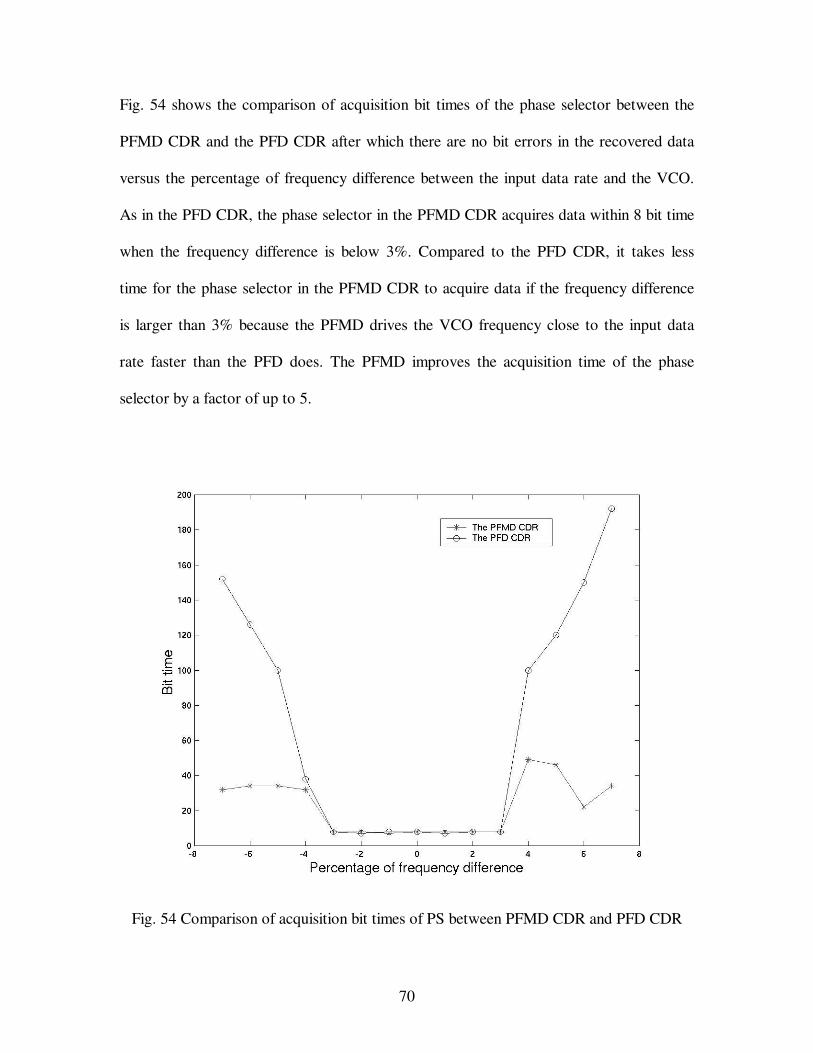
70
Fig. 54 shows the comparison of acquisition bit times of the phase selector between the
PFMD CDR and the PFD CDR after which there are no bit errors in the recovered data
versus the percentage of frequency difference between the input data rate and the VCO.
As in the PFD CDR, the phase selector in the PFMD CDR acquires data within 8 bit time
when the frequency difference is below 3%. Compared to the PFD CDR, it takes less
time for the phase selector in the PFMD CDR to acquire data if the frequency difference
is larger than 3% because the PFMD drives the VCO frequency close to the input data
rate faster than the PFD does. The PFMD improves the acquisition time of the phase
selector by a factor of up to 5.
Fig. 54 Comparison of acquisition bit times of PS between PFMD CDR and PFD CDR
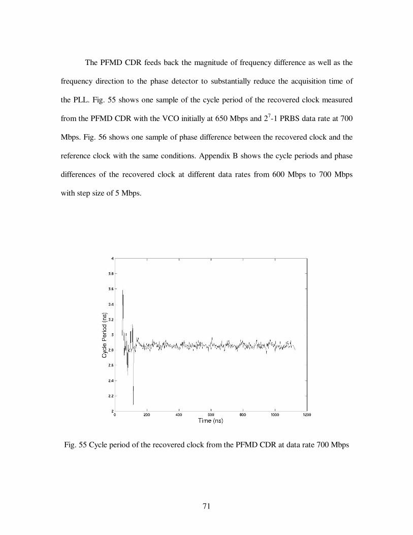
71
The PFMD CDR feeds back the magnitude of frequency difference as well as the
frequency direction to the phase detector to substantially reduce the acquisition time of
the PLL. Fig. 55 shows one sample of the cycle period of the recovered clock measured
from the PFMD CDR with the VCO initially at 650 Mbps and 27-1 PRBS data rate at 700
Mbps. Fig. 56 shows one sample of phase difference between the recovered clock and the
reference clock with the same conditions. Appendix B shows the cycle periods and phase
differences of the recovered clock at different data rates from 600 Mbps to 700 Mbps
with step size of 5 Mbps.
Fig. 55 Cycle period of the recovered clock from the PFMD CDR at data rate 700 Mbps
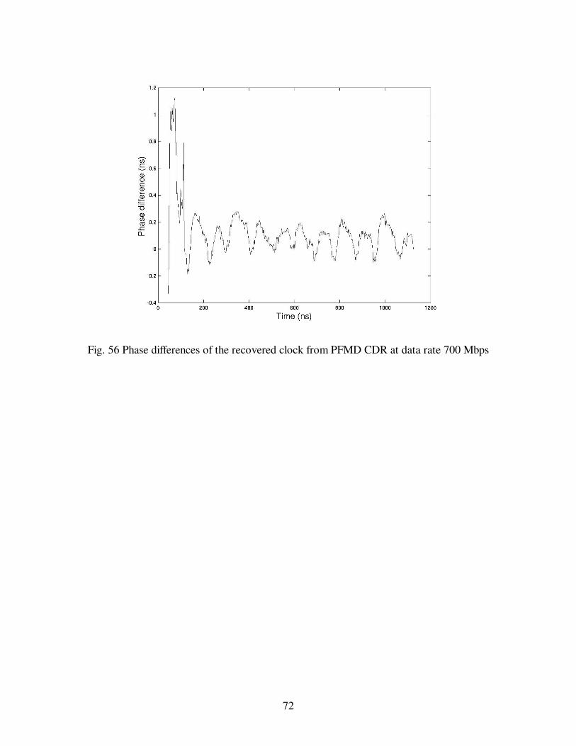
72
Fig. 56 Phase differences of the recovered clock from PFMD CDR at data rate 700 Mbps

73
Fig. 57 shows the averaged acquisition times of 50 samples of the PLL in the
PFMD CDR with the VCO initially at 645 Mbps and 27-1 PRBS data at different data
rates from 600 Mbps to 700 Mbps with step size of 1 Mbps. For a smaller frequency
difference it takes longer for a ½ bit time shift in the VCO phase with respect to the
incoming data. This delays the generation of the current pulse and contributes to the
acquisition time of the PFMD CDR being longer in the range from 2% to 4%. For
frequency differences less than 2%, the PLL locks before the PFMD applies its pulse.
Fig. 57 Acquisition times of the PLL in the PFMD CDR with VCO initially at 645 Mbps
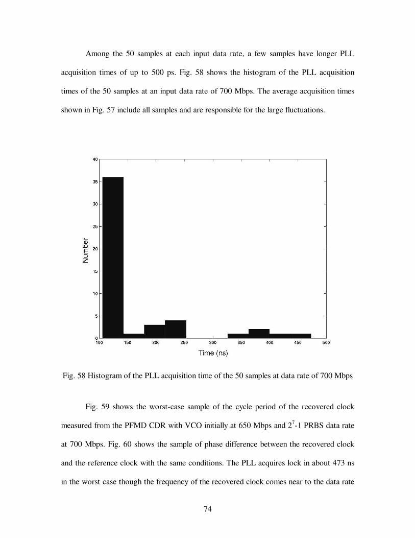
74
Among the 50 samples at each input data rate, a few samples have longer PLL
acquisition times of up to 500 ps. Fig. 58 shows the histogram of the PLL acquisition
times of the 50 samples at an input data rate of 700 Mbps. The average acquisition times
shown in Fig. 57 include all samples and are responsible for the large fluctuations.
Fig. 58 Histogram of the PLL acquisition time of the 50 samples at data rate of 700 Mbps
Fig. 59 shows the worst-case sample of the cycle period of the recovered clock
measured from the PFMD CDR with VCO initially at 650 Mbps and 27-1 PRBS data rate
at 700 Mbps. Fig. 60 shows the sample of phase difference between the recovered clock
and the reference clock with the same conditions. The PLL acquires lock in about 473 ns
in the worst case though the frequency of the recovered clock comes near to the data rate
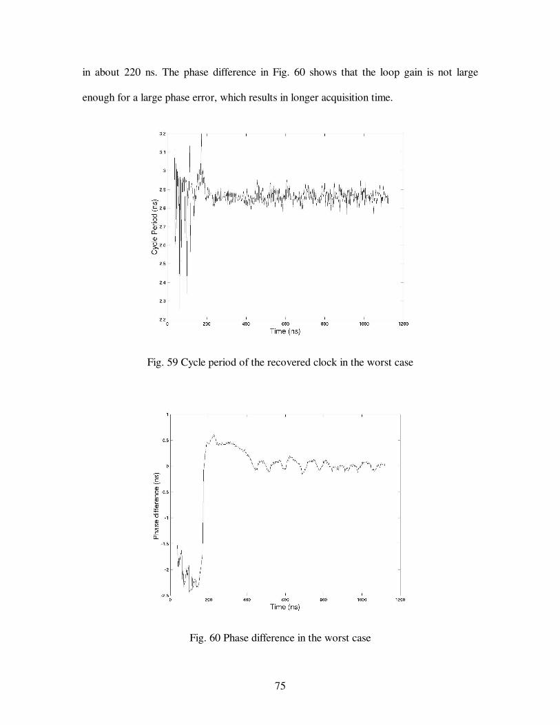
75
in about 220 ns. The phase difference in Fig. 60 shows that the loop gain is not large
enough for a large phase error, which results in longer acquisition time.
Fig. 59 Cycle period of the recovered clock in the worst case
Fig. 60 Phase difference in the worst case
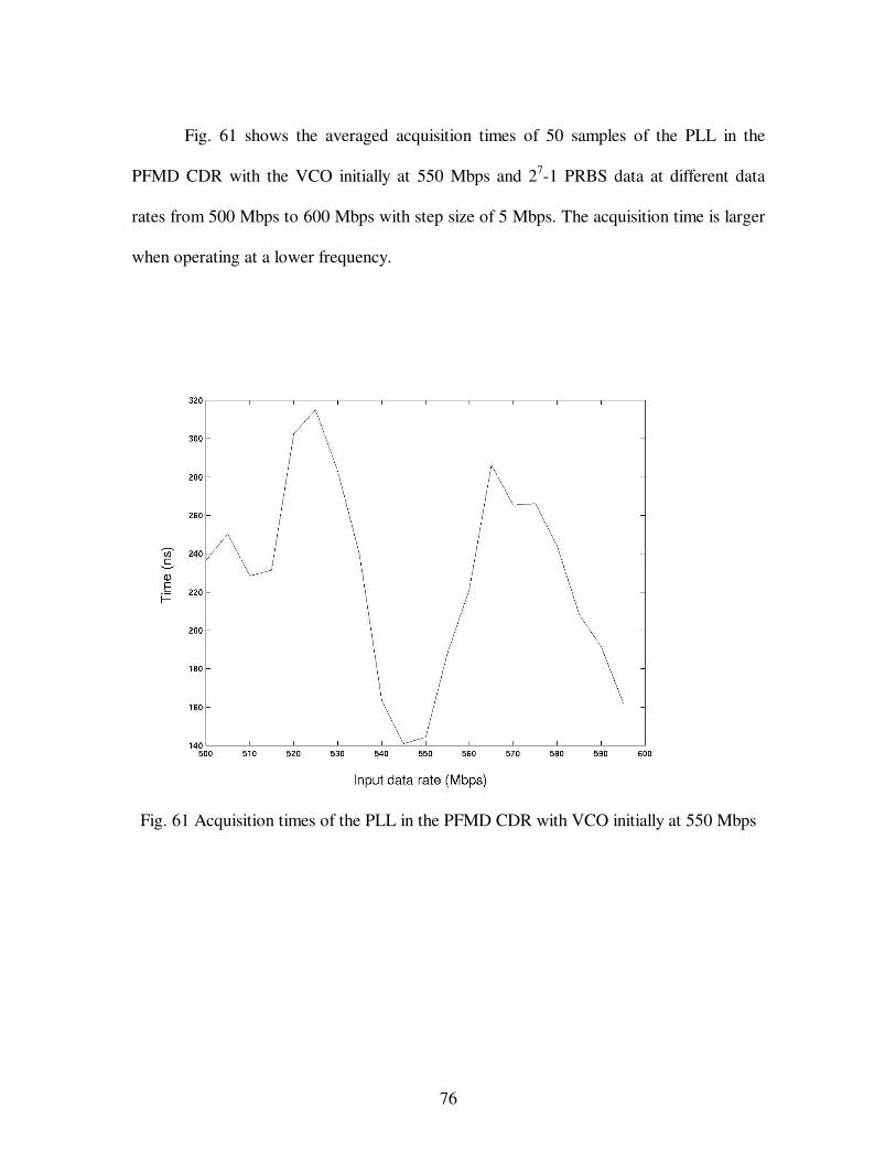
76
Fig. 61 shows the averaged acquisition times of 50 samples of the PLL in the
PFMD CDR with the VCO initially at 550 Mbps and 27-1 PRBS data at different data
rates from 500 Mbps to 600 Mbps with step size of 5 Mbps. The acquisition time is larger
when operating at a lower frequency.
Fig. 61 Acquisition times of the PLL in the PFMD CDR with VCO initially at 550 Mbps
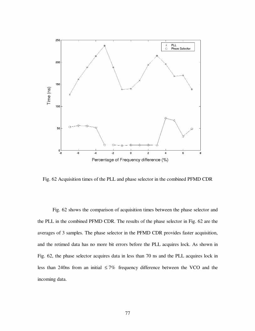
77
Fig. 62 Acquisition times of the PLL and phase selector in the combined PFMD CDR
Fig. 62 shows the comparison of acquisition times between the phase selector and
the PLL in the combined PFMD CDR. The results of the phase selector in Fig. 62 are the
averages of 3 samples. The phase selector in the PFMD CDR provides faster acquisition,
and the retimed data has no more bit errors before the PLL acquires lock. As shown in
Fig. 62, the phase selector acquires data in less than 70 ns and the PLL acquires lock in
less than 240ns from an initial %7≤ frequency difference between the VCO and the
incoming data.
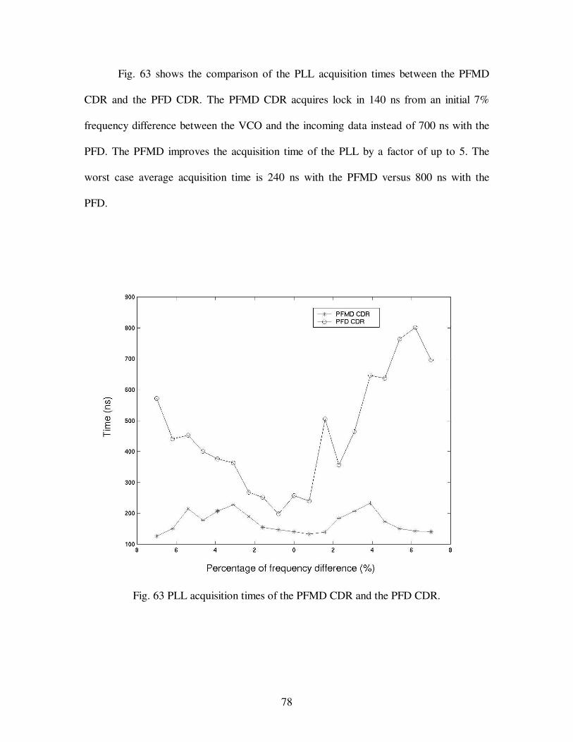
78
Fig. 63 shows the comparison of the PLL acquisition times between the PFMD
CDR and the PFD CDR. The PFMD CDR acquires lock in 140 ns from an initial 7%
frequency difference between the VCO and the incoming data instead of 700 ns with the
PFD. The PFMD improves the acquisition time of the PLL by a factor of up to 5. The
worst case average acquisition time is 240 ns with the PFMD versus 800 ns with the
PFD.
Fig. 63 PLL acquisition times of the PFMD CDR and the PFD CDR.

79
4.5 Output waveforms and jitter of the CDR
Fig. 64 shows one channel of the demultiplexed data output and the recovered
clock at 688 Mbps measured from the CDR with a sampling oscilloscope. Fig. 65 shows
the jitter histogram of the recovered clock in response to 688 Mbps 27-1 PRBS data as
measured by the sampling oscilloscope. The recovered clock has an rms jitter of 16 ps,
including the input jitter.
Fig. 64 Recovered data and clock output
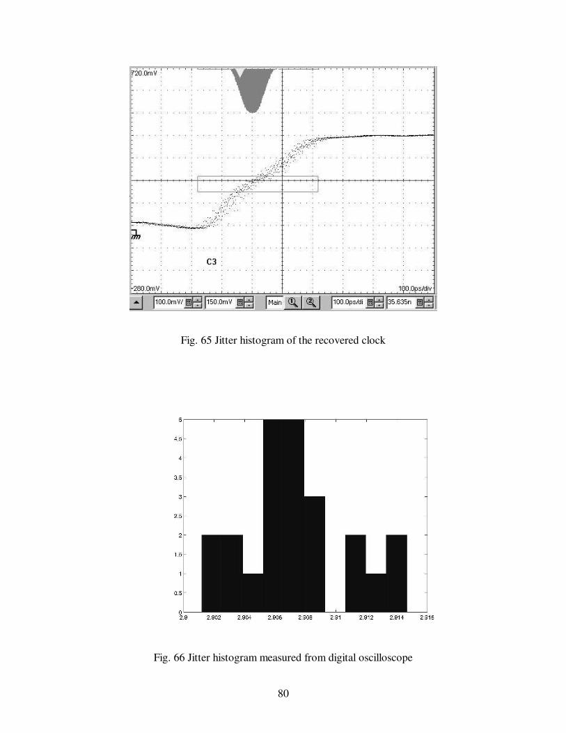
80
Fig. 65 Jitter histogram of the recovered clock
Fig. 66 Jitter histogram measured from digital oscilloscope
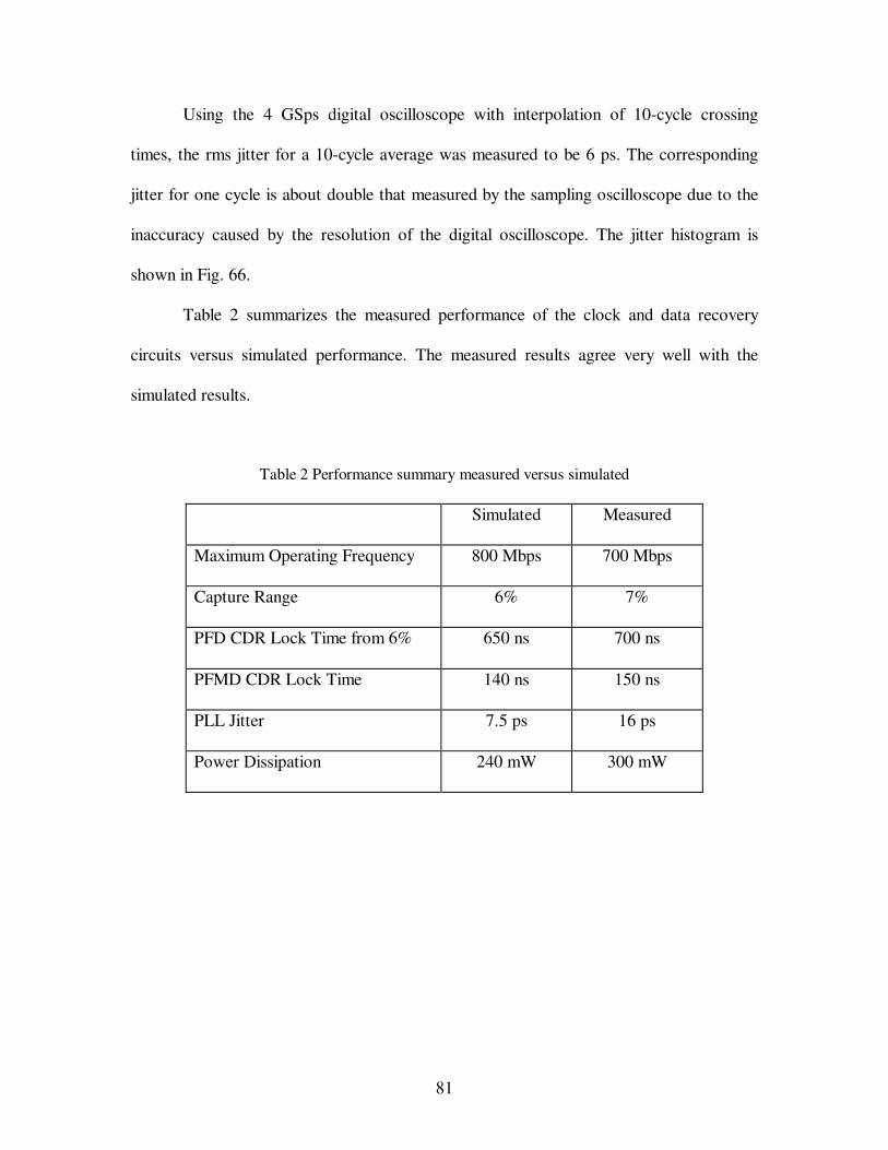
81
Using the 4 GSps digital oscilloscope with interpolation of 10-cycle crossing
times, the rms jitter for a 10-cycle average was measured to be 6 ps. The corresponding
jitter for one cycle is about double that measured by the sampling oscilloscope due to the
inaccuracy caused by the resolution of the digital oscilloscope. The jitter histogram is
shown in Fig. 66.
Table 2 summarizes the measured performance of the clock and data recovery
circuits versus simulated performance. The measured results agree very well with the
simulated results.
Table 2 Performance summary measured versus simulated
Simulated Measured
Maximum Operating Frequency 800 Mbps 700 Mbps
Capture Range 6% 7%
PFD CDR Lock Time from 6% 650 ns 700 ns
PFMD CDR Lock Time 140 ns 150 ns
PLL Jitter 7.5 ps 16 ps
Power Dissipation 240 mW 300 mW
82
CHAPTER FIVE
CONCLUSION
Clock and data recovery circuits have been widely used in data communication
systems. Acquisition time and jitter are two important issues in the design of the clock
and data recovery circuits. For networks with fast switching between nodes, short
acquisition time reduces the number of preamble bits required and results in higher
efficiency. Low jitter is important for low bit-error rate in the transfer of data. However,
there is trade-off between low jitter and short acquisition time. Phase locked loop
architectures offer low clock jitter after acquiring lock resulting in low error rates but
their acquisition times are long. Delay locked loop CDRs can lock to the data in just a
few clock cycles but have high jitter that results in higher error rates.
A combined phase-selector / PLL CDR was designed which consists of a phase
selector, which can lock to the data in just a few clock cycles but has high jitter, and a
PLL, which requires a much longer acquisition time but provides a low-jitter clock after
locking. A novel phase frequency magnitude detection circuit is also introduced to
substantially reduce the PLL acquisition time.
In 0.5 µm CMOS technology, a combined CDR was designed to operate in four
different modes: 1) a conventional analog PLL CDR, which has projected clock jitter of
about 8 ps but a fairly long acquisition time and small capture range of 1.5%, 2) a phase
selector CDR which has high jitter of 25% of a bit time but acquires data in 8 bit times, 3)
a novel CDR that combines a PLL with a phase selector that acquires data in 8 bit times,
has high jitter to start but the jitter reduces to that of the PLL (~8 ps) after the PLL
acquires lock in about 650 ns from the initial 6% frequency difference, and 4) a novel

83
PFMD circuit that applies only a single pulse, with an amplitude based on the estimated
frequency difference, to the charge pump of the PLL reducing the expected acquisition
time of the PLL to under 200ns from the initial 6% frequency difference between the
input data and the recovered clock.
Measurement results of the combined CDR show functionality in all four modes
up to 700 Mbps. This is somewhat short of the 800 Mbps expected from simulation. The
capture range in mode 1 is about what was expected. The measured rms cycle-to-cycle
jitter of the PLL is 16 ps, including the input jitter. The simulated 8 ps rms jitter of the
PLL is only pattern-dependent jitter without including the input jitter. In mode 2, the
phase selector CDR acquires data in 8 bit times as expected and has high jitter of 30% of
a bit time that is close to the simulated jitter of 25% of a bit time.
In mode 3, the CDR combines a PLL with a phase selector that provides the
information of the frequency direction. The phase selector acquires data in 8 bit times
without bit error if the frequency difference between the input data and the VCO is below
3%. It takes longer for the phase selector to acquires data if the frequency difference is
from 3% to 7% because the phase selector has higher jitter of 50% of a bit time. The
phase selector initially has high jitter but the jitter reduces to that of the PLL (~16 ps)
after the PLL acquires lock. The PFD drives the VCO close to the input data rate and the
PLL acquires lock in about 700 ns from the initial frequency difference of 7%.
In mode 4, the PFMD reduces the acquisition time of the PLL to 140 ns from an
initial 7% frequency difference compared to 700 ns with the PFD circuit. The phase
selector in the combined PFMD CDR acquires data in 8 bit times without bit error if the
frequency difference is below 3%. Compared to the acquisition time of the phase selector
84
in the PFD CDR, it takes less time for the phase selector of the PFMD CDR to acquire
data because the PFMD circuit drives the VCO faster to the input data than the PFD does.
85
BIBLIOGRAPHY
[1] B. Razavi, Design of integrated circuits for optical communications, Chicago: McGraw Hill, 2002.
[2] B. Razavi, “Design of monolithic phase-locked loops and clock recovery circuits-a
tutorial,” in Monolithic Phase-locked loops and Clock recovery circuits: Theory and Design, New York, NY: IEEE Press, 1996.
[3] S. B. Anand and B. Razavi, “A CMOS clock recovery circuit for 2.5-Gb/s NRZ
data,” IEEE J. Solid-State circuits, vol. 36, pp. 432-439, March 2001. [4] M. Rau, T. Oberst, R. Lares, A. Rothermel, R. Schweer, and N. Menoux,
“Clock/data recovery PLL using half-frequency clock,” IEEE J. Solid-State Circuits, vol. 32, pp. 1156-1160, July 1997.
[5] J. Savoj and B. Razavi, “A 10-Gb/s CMOS clock and data recovery circuit with a
half-rate linear phase detector,” IEEE J. Solid-State Circuits, vol. 36, pp. 761-768, May 2001.
[6] N. Ishihara and Y. Akazawa, “A monolithic 156 Mb/s clock and data recovery PLL
circuit using the sample-and-hold technique,” IEEE J. Solid-State Circuits, vol. 29, pp. 1566-1571, Dec. 1994.
[7] K. Ishii, K. Kishine, and H. Ichino, “A jitter suppression technique for a 2.48832-
Gb/s clock and data recovery circuit,” IEEE Trans. Circuits Syst. II, vol 49, pp. 266-272, April 2002.
[8] K. Kishine, N. Ishihara, K. Takiguchi, and H. Ichino, “A 2.5-Gb/s clock and data
recovery IC with tunable jitter characteristics for use in LAN’s and WAN’s,” IEEE J. Solid-State Circuits, vol. 34, pp. 805-812, June 1999.
[9] D. Richman, “Color-carrier reference phase synchronization accuracy in NTSC
color television,” Proc. IRE, vol. 42, pp. 106-133, Jan. 1954. [10] J. A. Bellisio, “A new phase-locked loop timing recovery method for digital
regenerators,” IEEE Int. Conf. Rec., vol. 1, pp. 10-17, June 1976. [11] B. Razavi, “A 2.5-Gb/s 15mW clock recovery circuit,” IEEE J. Solid-State Circuits,
vol. 31, pp. 472-480, April 1996. [12] A. Pottbacker, U. Langmann, and H.-U. Schreiber, “A Si bipolar phase and
frequency detector IC for clock extraction up to 8 Gb/s,” IEEE J. Solid-State Circuits, vol. 27, pp. 1747-1751, Dec. 1992.
86
[13] J. C. Scheytt, G. Hanke, and U. Langmann, “A 0.155-, 0.622-, and 2.488-Gb/s automatic bit-rate selecting clock and data recovery IC for bit-rate transparent SDH systems,” IEEE J. Solid-State Circuits, vol. 34, pp. 1935-1943, Dec. 1999.
[14] H. Djahanshahi and C. A. T. Salama, “Differential CMOS circuits for 622-
MHz/933-MHz clock and data recovery applications,” IEEE J. Solid-State Circuits, vol. 35, pp. 847-855, June 2000.
[15] H. Ransijn and P. O’Connor, “A PLL-based 2.5-Gb/s GaAs clock and data
regenerator IC,” IEEE J. Solid-State Circuits, vol. 26, pp. 1345-1353, Oct. 1991. [16] J. Savoj and B. Razavi, “A 10 Gb/s CMOS clock and data recovery circuit with a
half-rate binary phase/frequency detector,” IEEE J. of Solid-State Circuits, vol. 38, pp. 13-21, Jan. 2003.
[17] K. Kishine, N. Ishihara, and H. Ichino, “Techniques for widening lock and pull-in
ranges and suppressing jitter in clock and data recovery ICs-Duplicated loop control CDR,” IEIEC Trans. Electron., Vol.E84-C, April 2001.
[18] H. Wang and R. Nottenburg, “A 1Gb/s CMOS clock and data recovery circuit,”
IEEE Int. Solid-State Circuits Conf. Dig. Tech. Papers, 1999. [19] S. Y. Sun, “An analog PLL-base clock and data recovery circuit with high input
jitter tolerance,” IEEE J. of Solid-State Circuits, vol. SC-24, pp. 325-330, April 1989.
[20] D.-H. Kim and J.-K. Kang, “Clock and data recovery circuit with two exclusive-OR
phase frequency detector,” Electron. Lett., vol. 36, pp. 1347-1349, Aug. 2000. [21] D. G. Messerschmitt, “Frequency detectors for PLL acquisition in timing and
carrier recovery,” IEEE Trans. Comm., vol. COM-27, pp. 1288-1295, Sep. 1979. [22] C. R. Hogge, “A self-correcting clock recovery circuit,” IEEE J. Lightwave
Technology, vol. LT-3, pp. 1312-1314, Dec. 1985. [23] J. Lee and B. Kim, “A Low Noise Fast-Lock Phase-Locked Loop with Adaptive
Bandwidth Control,” IEEE J. Solid-State Circuits, vol. 35, pp.1137-1145, Aug. 2000.
[24] J. Sonntag and R. Leonowich, “ A monolithic CMOS 10 MHz DPLL for burst-
mode data retiming,” in Proc. IEEE ISSCC, 1990, pp. 194-195. [25] B. Garlepp, K. Donnelly, J. Kim, P. Chau, J. Zerbe, C. Huang, C. Tran, C.
Portmann, D. Stark, Y. Chan, T. Lee, and M. Horowitz, “A portable digital DLL for high-speed CMOS interface circuits,” IEEE J. Solid-State Circuits, Vol. 34, pp. 632-644, May 1999.
87
[26] T. Hsu, B. Shieh, and C. Lee, “An all-digital phase-locked loop (ADPLL)-based
clock recovery circuit,” IEEE J. Solid-State Circuits, Vol. 34, pp. 1063-1073, Aug. 1999.
[27] P. Larsson, “A 2-1600-MHz CMOS clock recovery PLL with low-Vdd capability,”
IEEE J. Solid-State Circuits, Vol. 34, pp. 1951-1960, Dec. 1999. [28] X. maillard, F. Devisch, and M. Kuijk, “A 900-Mb/s CMOS data recovery DLL
using half-frequency clock,” IEEE J. Solid-State Circuits, Vol. 37, pp. 711-715, June 2002.
[29] T. H. Lee, K. S. Donnelly, J. T. C. Ho, J. Zerbe, M. G. Johnson, and T. Ishikawa,
“A 2.5 V CMOS delay-locked loop for an 18 Mbit, 500 Megabyte/s DRAM,” IEEE J. Solid-State Circuits, Vol. 29, pp. 1491-1496, Dec. 1994.
[30] S. Sidiropoulos and M. A. Horowitz, “A semidigital dual delay-locked loop,” IEEE
J. Solid-State Circuits, Vol. 32, pp. 1683-1692, Nov. 1997. [31] T. Hamamoto, K. Furutani, T. Kubo, S. Kawasaki, H. Iga, T. Kono, Y. Konishi and
T. Yoshihara, “A 667-Mb/s operating digital DLL architecture for 512-Mb DDR SDRAM,” IEEE J. Solid-State Circuits, Vol. 39, pp. 194-206, Jan. 2004.
[32] J. G. Maneatis, “Low-jitter process-independent DLL and PLL based on self-biased
techniques,” IEEE J. Solid-State Circuits, Vol. 31, pp. 1723-1732, Nov. 1996. [33] T. Kim, S. Wang, and B. Kim, “A Low Jitter, Fast Locking Delay Locked Loop
Using Measure and Control Scheme,” 2001 Southwest Symposium on Mixed-Signal Design.
[34] B. Kim, D. N. Helman, and P. R. Gray, “A 30-MHz hybrid analog/digital clock
recovery circuit in 2-µm CMOS,” IEEE J. Solid-State Circuits, Vol. 25, pp. 1385-1394, Dec. 1990.
[35] T. H. Lee and J. F. Bulzacchelli, “A 155-MHz clock recovery delay- and phase-
locked loop,” IEEE J. Solid-State Circuits, Vol. 27, pp. 1736-1746, Dec. 1992.
[36] B. Razavi, “Challenges in the design of high-speed clock and data recovery circuits,” IEEE Communications Magazine, pp. 94-101, Aug. 2002.
[37] A. Blanchard, Phase-Locked Loops: Application to Coherent Receiver Design, New
York: Wiley, 1976. [38] F. M. Gardner, Phaselock Techniques, New York: Wiley, 1966.
88
[39] R. E. Best, Phase-Locked Loops: Theory, Design, and Applications, New York: McGraw Hill, 1984.
[40] B. Razavi, Design of Analog CMOS Integrated Circuits, New York: McGraw Hill,
2001. [41] N. Roberts, “Phase noise and jitter – a primer for digital designers,” EE Design,
July 14, 2003. [42] J. McNeill, “A simple method for relating time- and frequency-domain measures of
oscillator performance,” Proceedings of the 2001 IEEE Southwest Symposium on Mixed Signal Design, Feb. 2001.
[43] R. Zhang and G. La Rue, "Clock and Data Recovery Circuits with Fast Acquisition
and Low Jitter," Proc. University/Government/Industry Microelectronics Symposium, 15th Biennial, June 2003, pp. 82-85.
[44] R. Zhang and G. La Rue, "Clock and Data Recovery Circuits with Fast Acquisition
and Low Jitter," 2004 IEEE Workshop on Microelectronics and Electron Devices, 16 April 2004, pp. 48 - 51

89
APPENDIX A.
Measurement Results of the Combined PFD CDR
Fig. A1 shows one of the 50 samples of the cycle period of the recovered clock
measured from the combined PFD CDR with the VCO initially at 600 Mbps and 27-1
PRBS data at different data rates from 555 Mbps to 650 Mbps with step size of 5 Mbps.
Fig. A2 shows one of the 50 samples of the phase difference between the recovered clock
and the reference clock with the same conditions.
(a) Input data rate at 555 Mbps
Fig. A1 Cycle period of the recovered clock from the PFD CDR at different data rates

90
(b) Input data rate at 560Mbps
(c) Input data rate at 565 Mbps
Fig. A1 (continued)
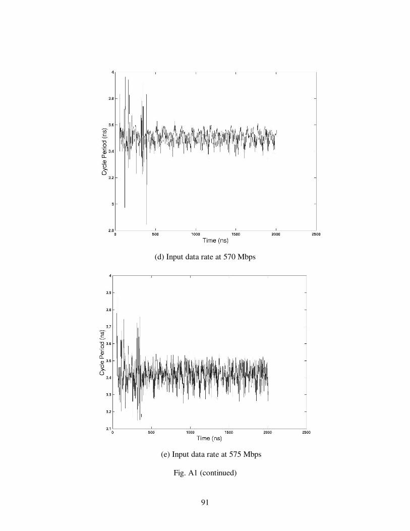
91
(d) Input data rate at 570 Mbps
(e) Input data rate at 575 Mbps
Fig. A1 (continued)
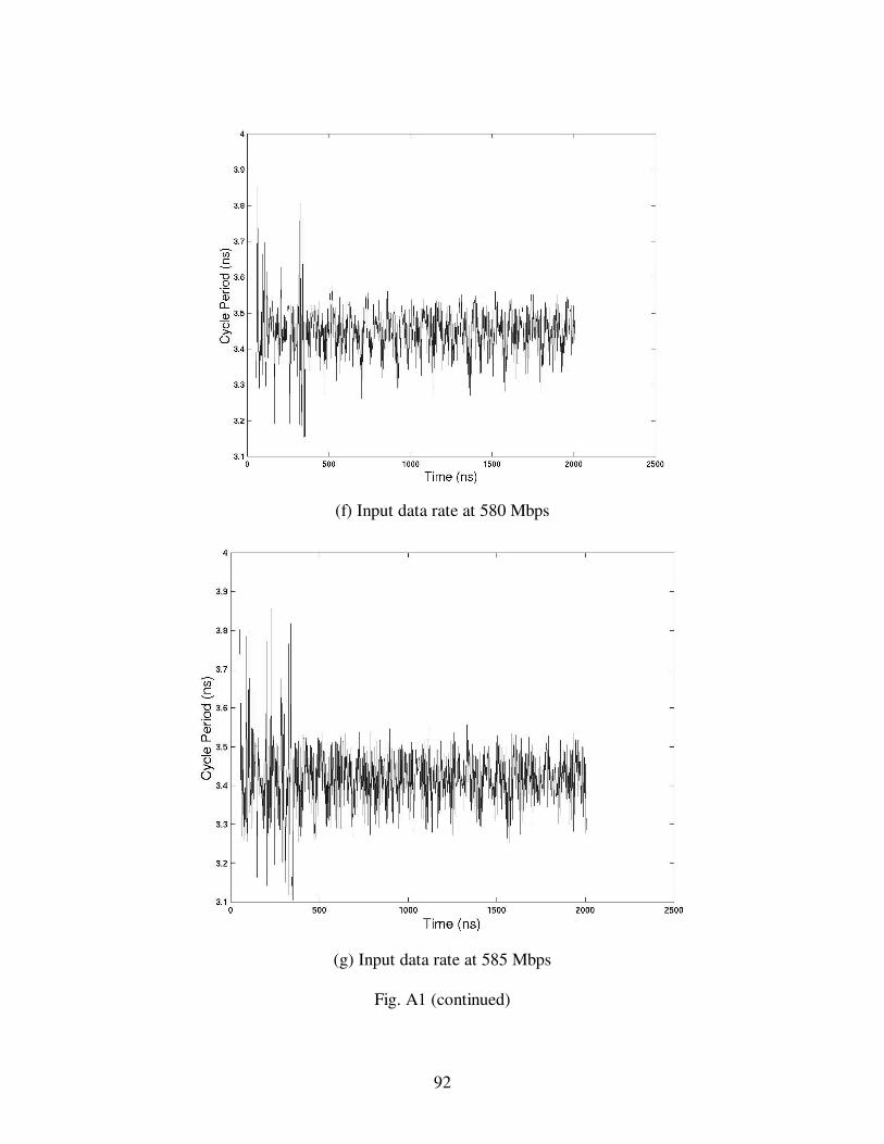
92
(f) Input data rate at 580 Mbps
(g) Input data rate at 585 Mbps
Fig. A1 (continued)
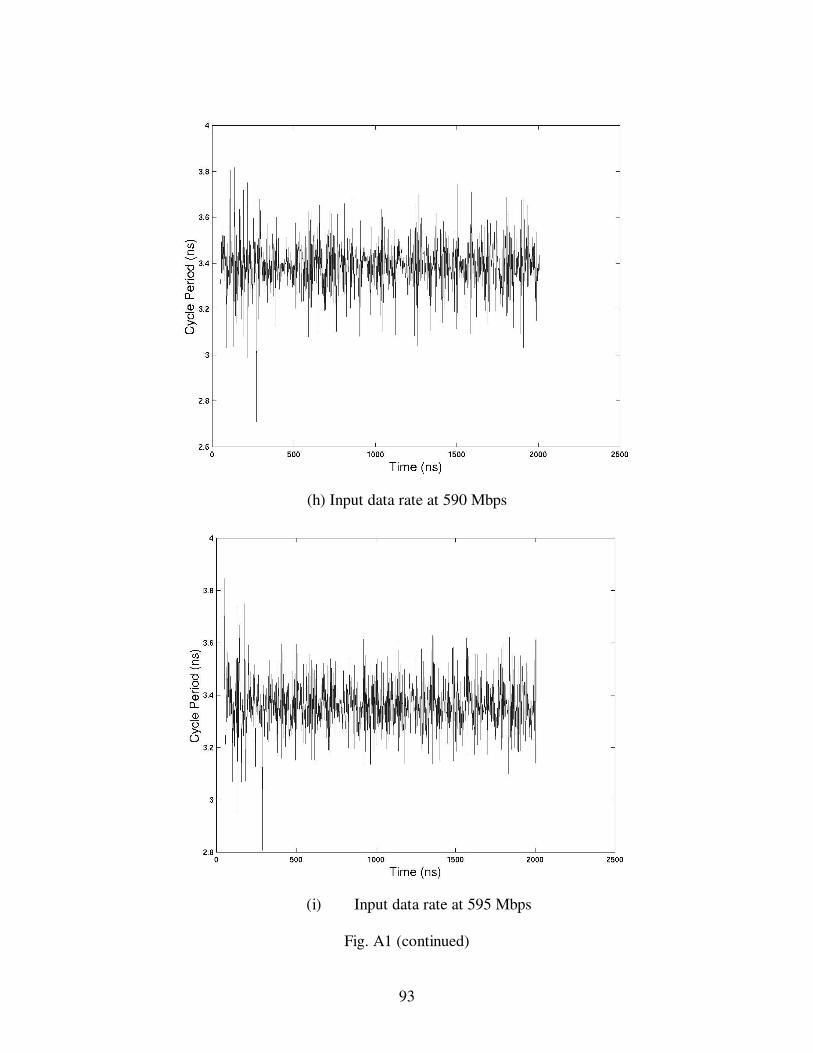
93
(h) Input data rate at 590 Mbps
(i) Input data rate at 595 Mbps
Fig. A1 (continued)
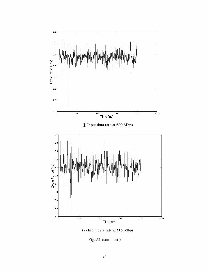
94
(j) Input data rate at 600 Mbps
(k) Input data rate at 605 Mbps
Fig. A1 (continued)
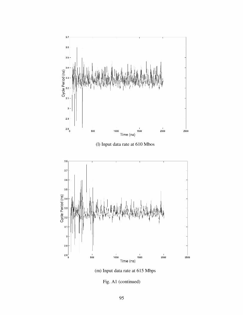
95
(l) Input data rate at 610 Mbos
(m) Input data rate at 615 Mbps
Fig. A1 (continued)
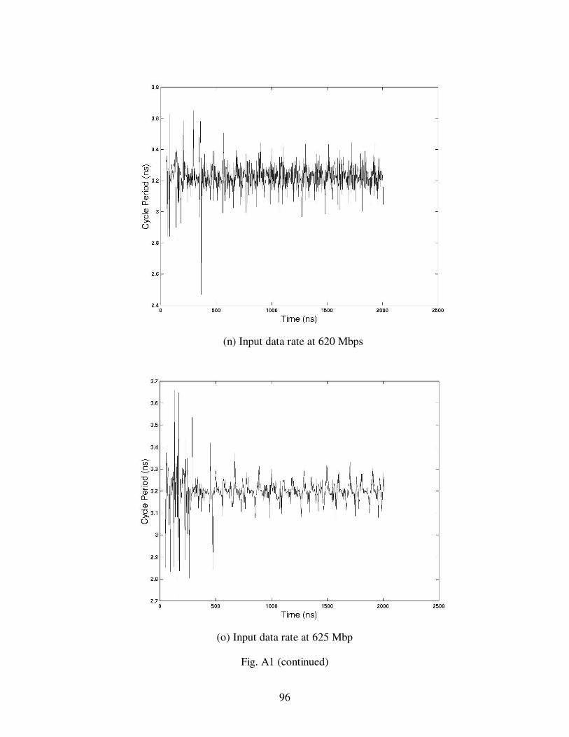
96
(n) Input data rate at 620 Mbps
(o) Input data rate at 625 Mbp
Fig. A1 (continued)
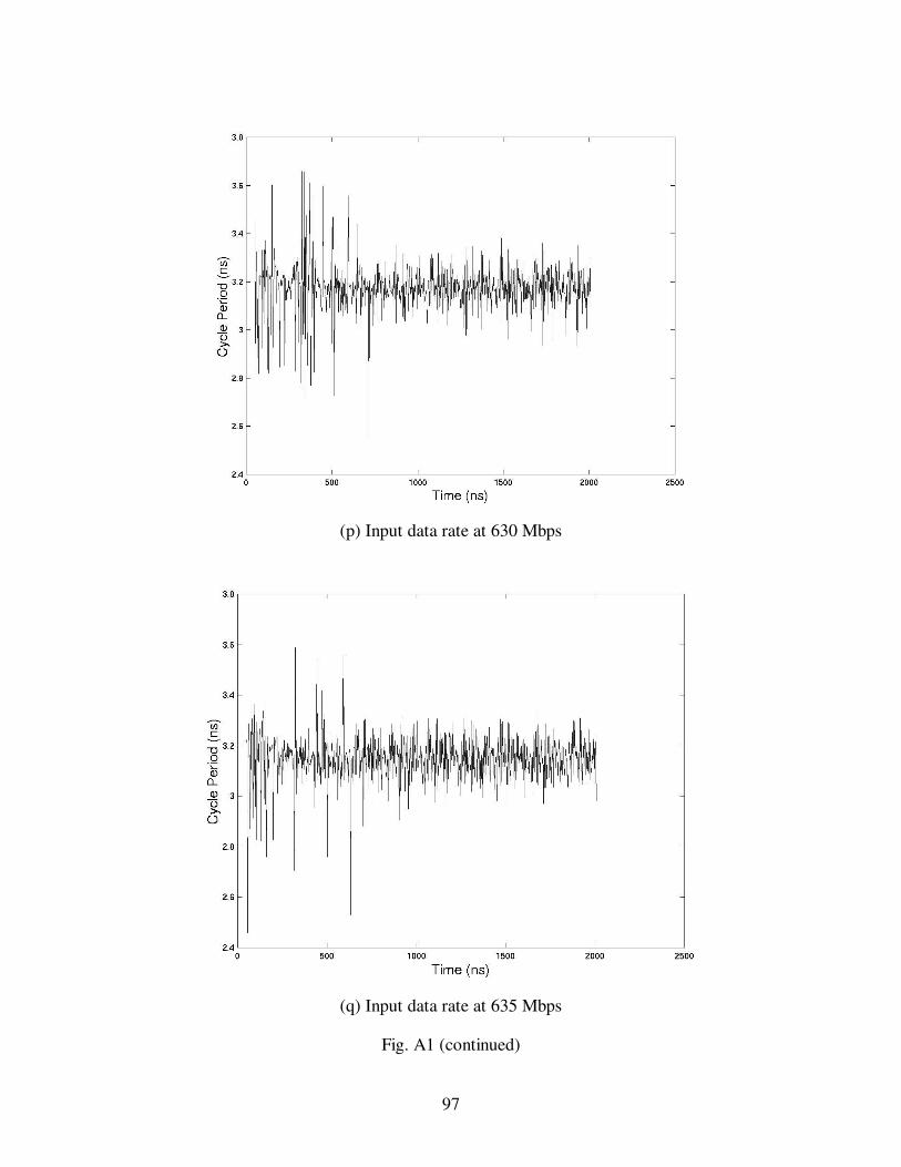
97
(p) Input data rate at 630 Mbps
(q) Input data rate at 635 Mbps
Fig. A1 (continued)
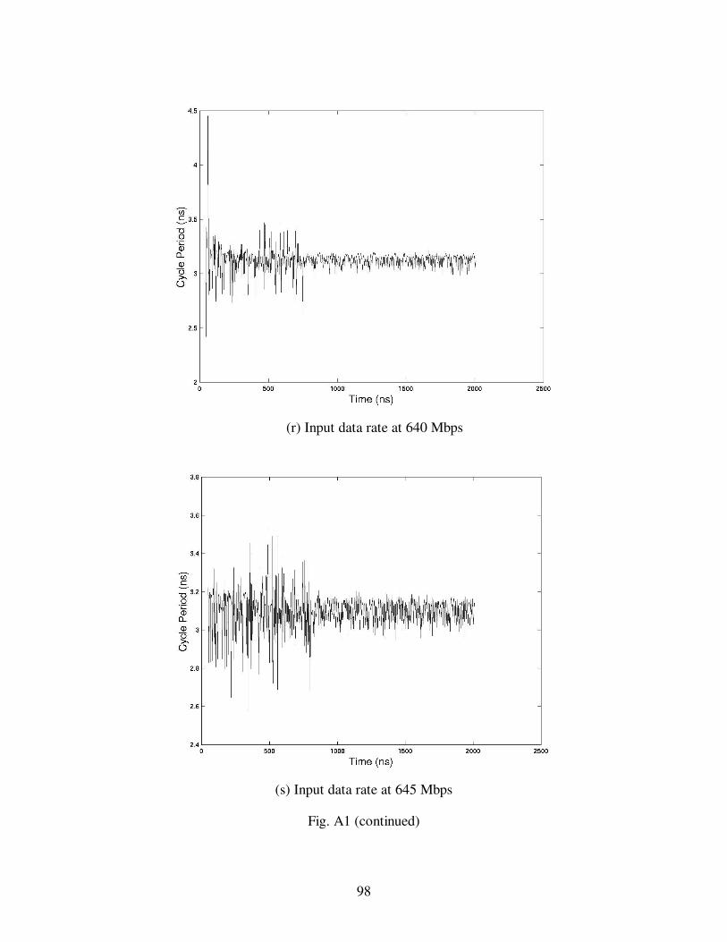
98
(r) Input data rate at 640 Mbps
(s) Input data rate at 645 Mbps
Fig. A1 (continued)
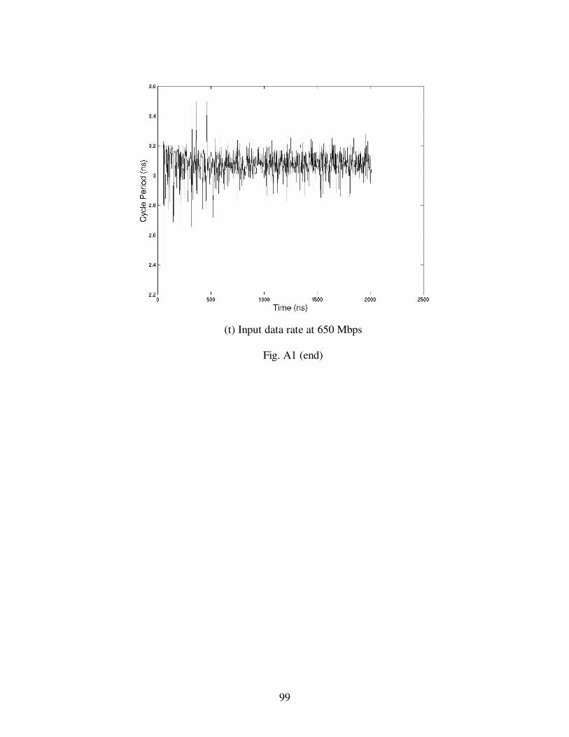
99
(t) Input data rate at 650 Mbps
Fig. A1 (end)
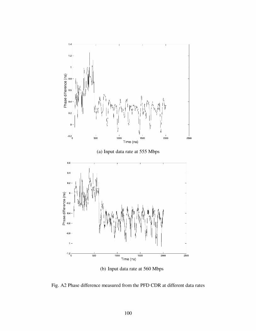
100
(a) Input data rate at 555 Mbps
(b) Input data rate at 560 Mbps
Fig. A2 Phase difference measured from the PFD CDR at different data rates
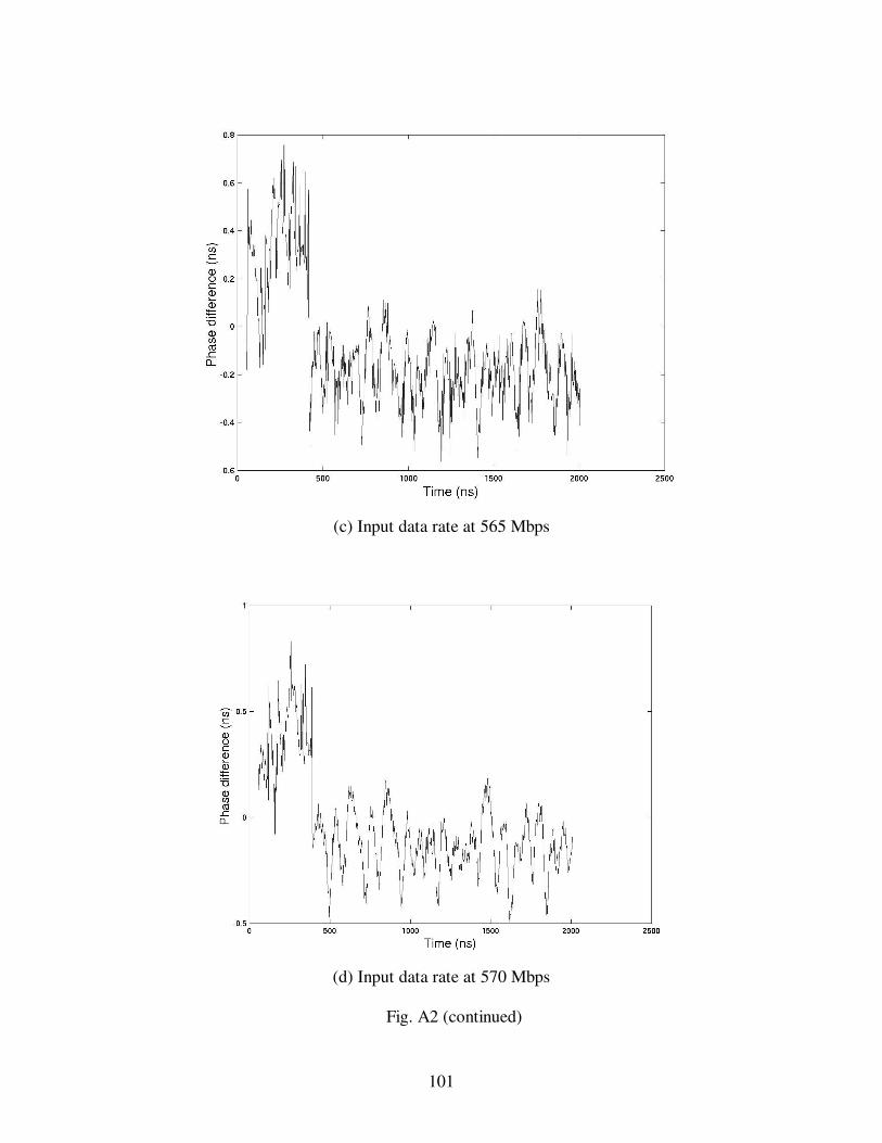
101
(c) Input data rate at 565 Mbps
(d) Input data rate at 570 Mbps
Fig. A2 (continued)
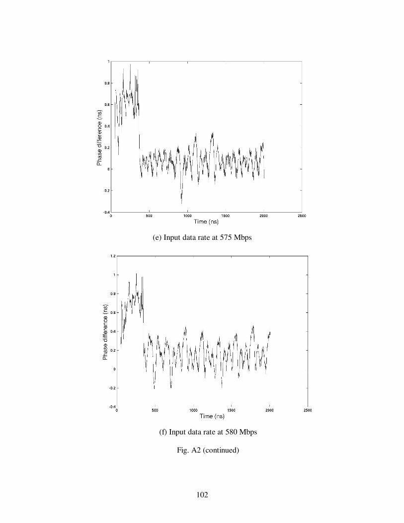
102
(e) Input data rate at 575 Mbps
(f) Input data rate at 580 Mbps
Fig. A2 (continued)
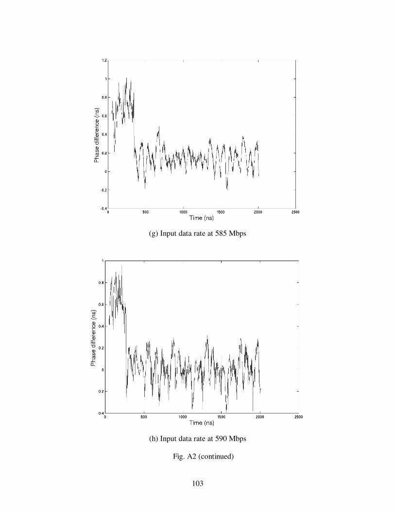
103
(g) Input data rate at 585 Mbps
(h) Input data rate at 590 Mbps
Fig. A2 (continued)
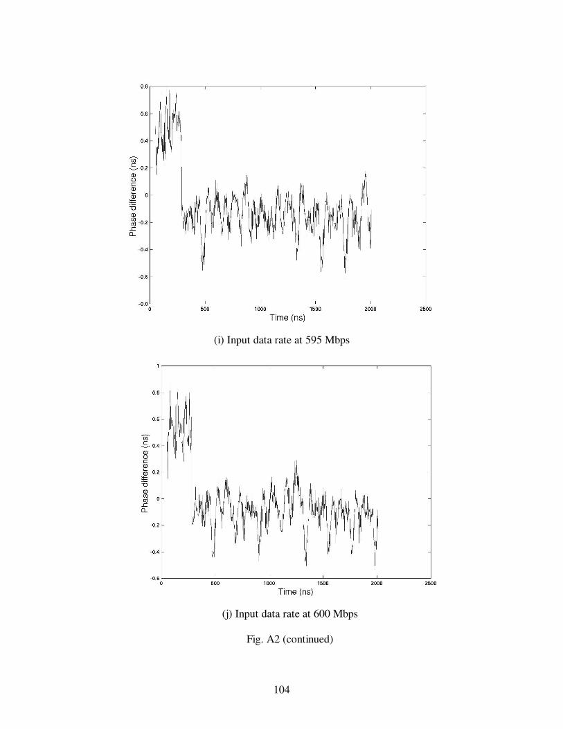
104
(i) Input data rate at 595 Mbps
(j) Input data rate at 600 Mbps
Fig. A2 (continued)
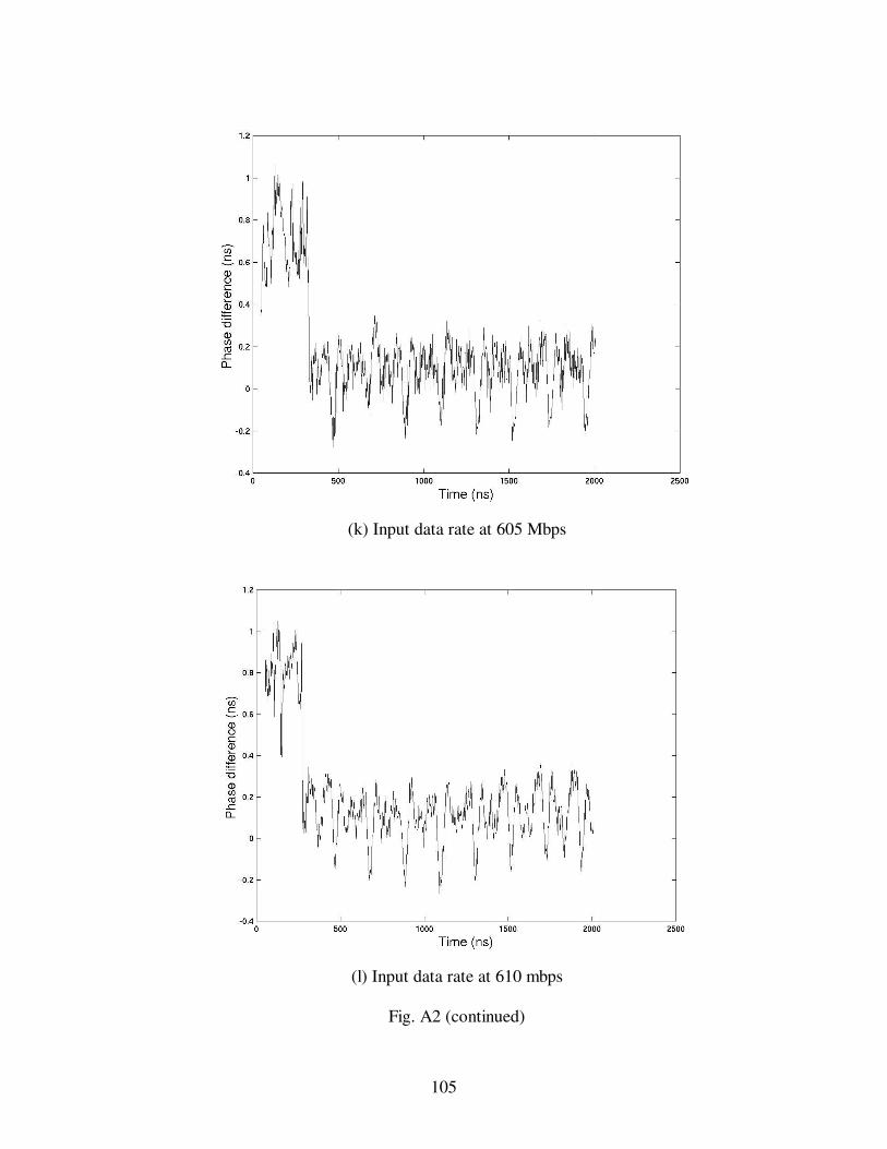
105
(k) Input data rate at 605 Mbps
(l) Input data rate at 610 mbps
Fig. A2 (continued)
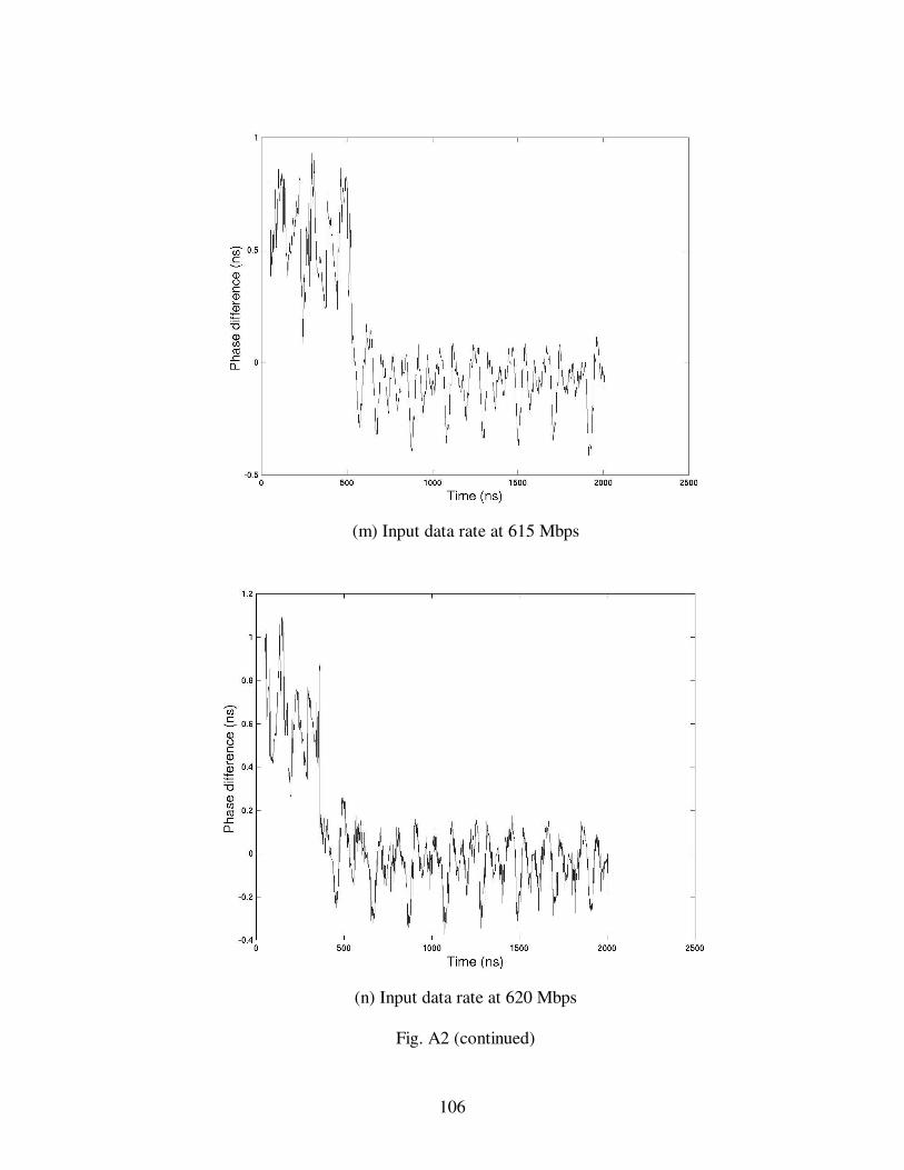
106
(m) Input data rate at 615 Mbps
(n) Input data rate at 620 Mbps
Fig. A2 (continued)

107
(o) Input data rate at 625 Mbps
(p) Input data rate at 630 Mbps
Fig. A2 (continued)
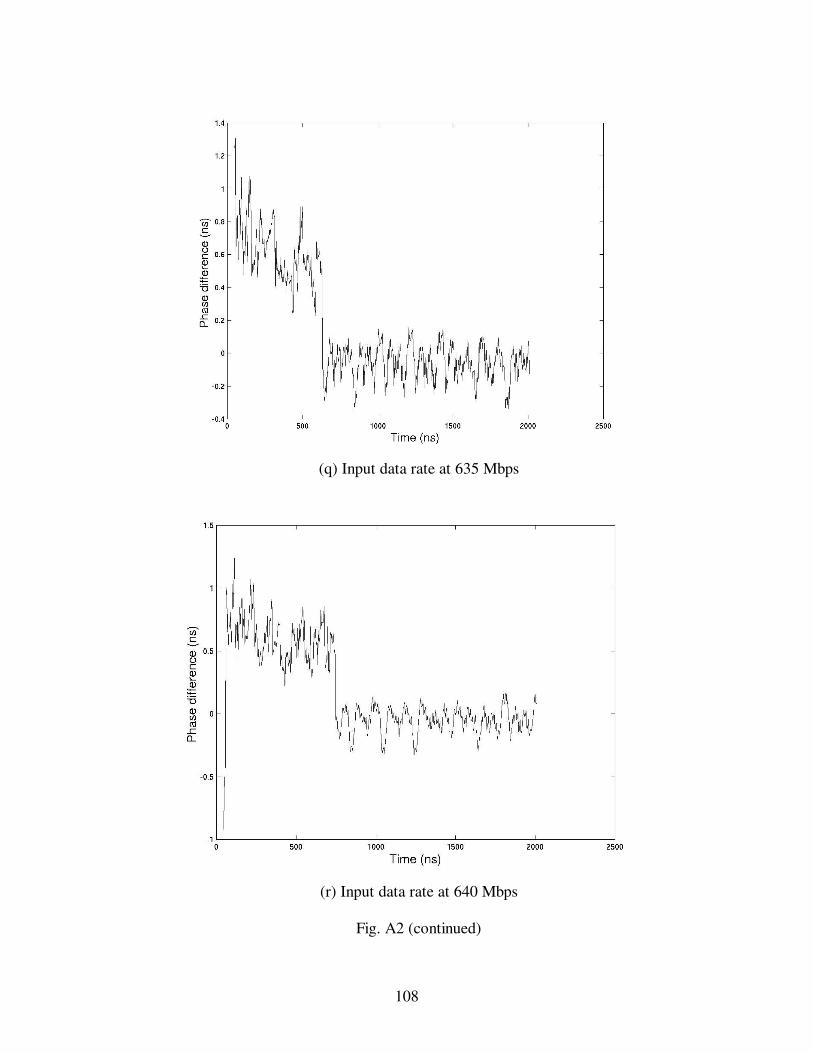
108
(q) Input data rate at 635 Mbps
(r) Input data rate at 640 Mbps
Fig. A2 (continued)
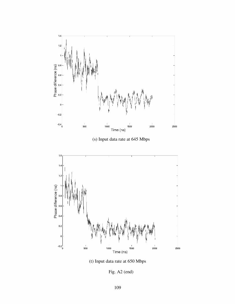
109
(s) Input data rate at 645 Mbps
(t) Input data rate at 650 Mbps
Fig. A2 (end)

110
APPENDIX B
Measurement Results of the PFMD CDR
Fig. B1 shows one of the 50 samples of the cycle periods of the recovered clock
measured from the PFMD CDR with VCO initially at 650 Mbps and 27-1 PRBS data at
different rates from 600 Mbps to 700 Mbps with step size of 5 Mbps. Fig. B2 shows one
of the 50 samples of the phase difference between the recovered clock and the reference
clock with same conditions.
(a) Input data rate at 600 Mbps
Fig. B1 Cycle periods of the recovered clock from the PFMD CDR at different data rates

111
(b) Input data rate at 605 Mbps
Input data rate at 610 Mbps
Fig. B1 (continued)
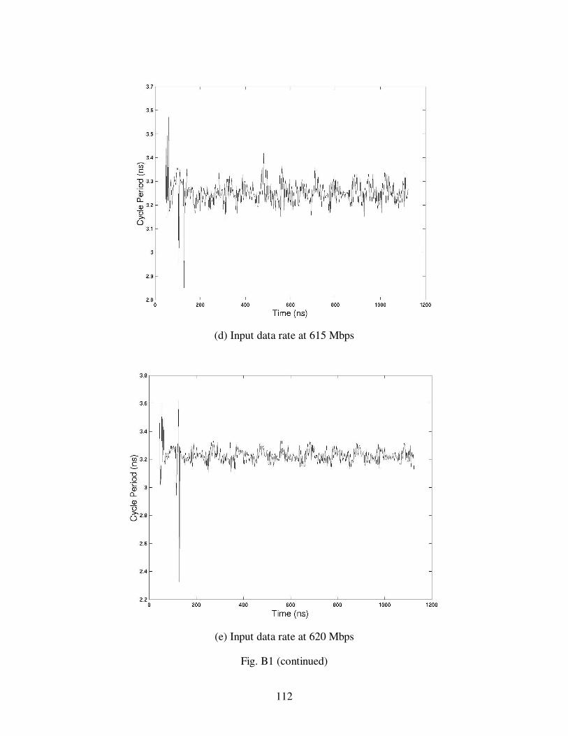
112
(d) Input data rate at 615 Mbps
(e) Input data rate at 620 Mbps
Fig. B1 (continued)
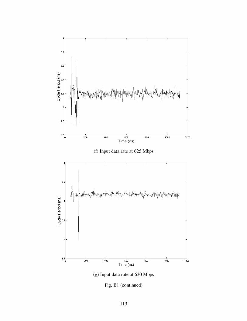
113
(f) Input data rate at 625 Mbps
(g) Input data rate at 630 Mbps
Fig. B1 (continued)
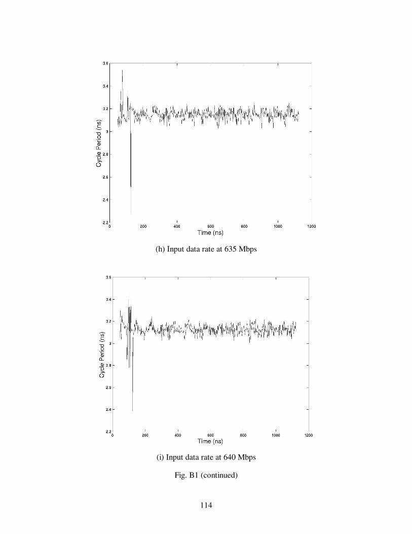
114
(h) Input data rate at 635 Mbps
(i) Input data rate at 640 Mbps
Fig. B1 (continued)
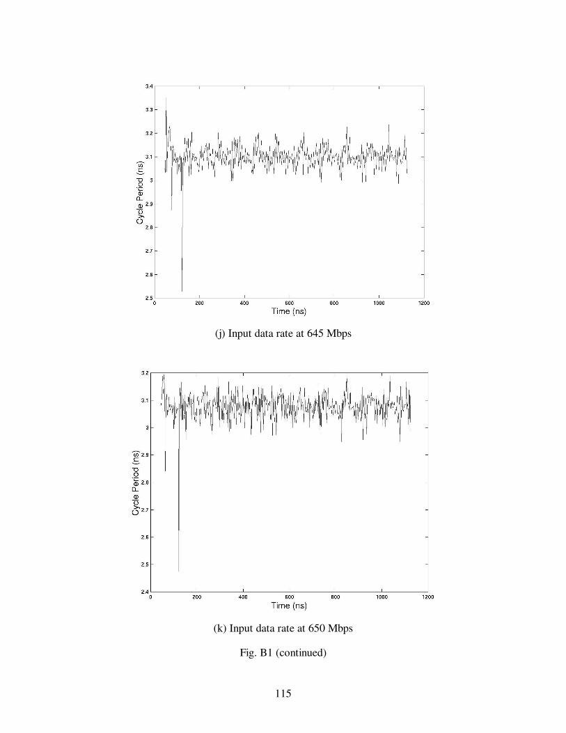
115
(j) Input data rate at 645 Mbps
(k) Input data rate at 650 Mbps
Fig. B1 (continued)
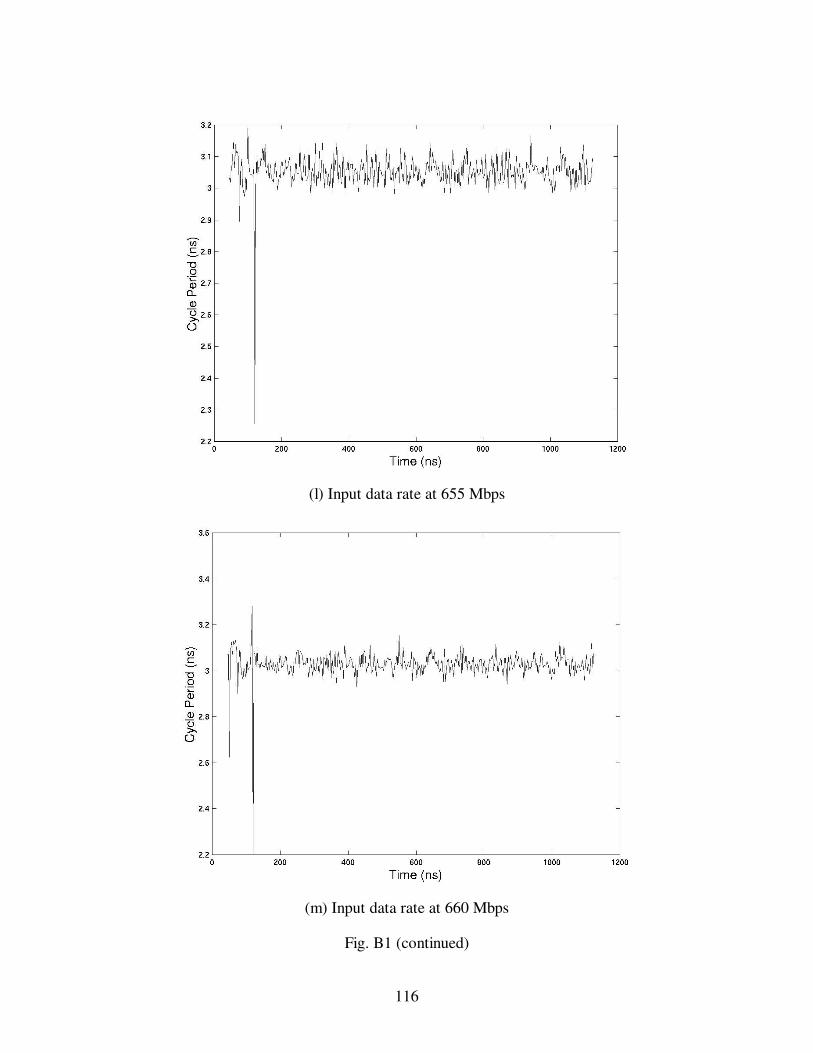
116
(l) Input data rate at 655 Mbps
(m) Input data rate at 660 Mbps
Fig. B1 (continued)
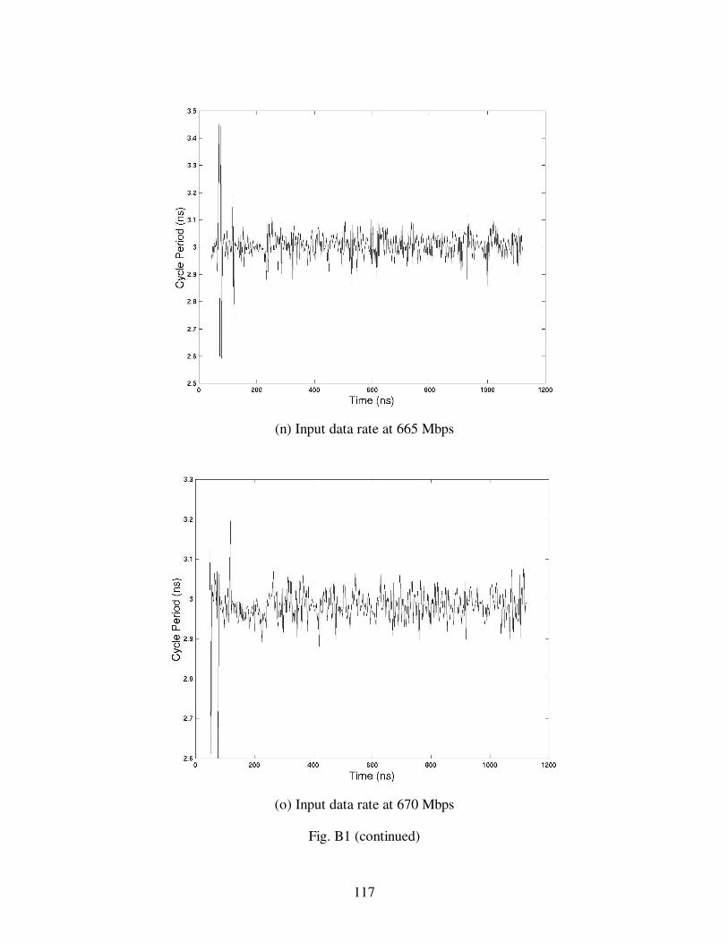
117
(n) Input data rate at 665 Mbps
(o) Input data rate at 670 Mbps
Fig. B1 (continued)
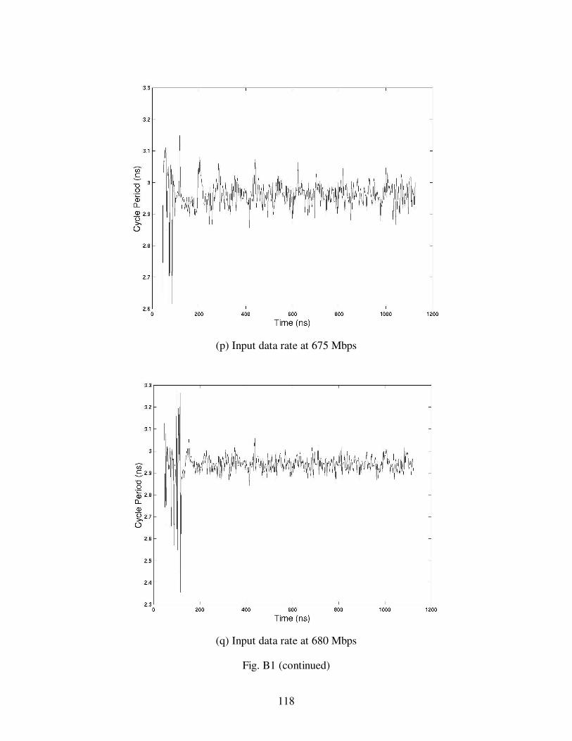
118
(p) Input data rate at 675 Mbps
(q) Input data rate at 680 Mbps
Fig. B1 (continued)
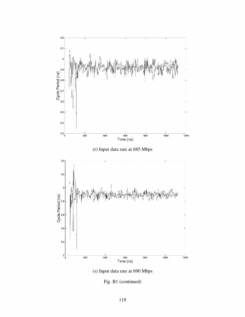
119
(r) Input data rate at 685 Mbps
(s) Input data rate at 690 Mbps
Fig. B1 (continued)
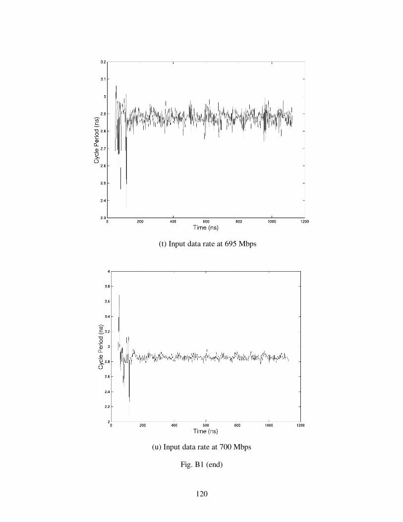
120
(t) Input data rate at 695 Mbps
(u) Input data rate at 700 Mbps
Fig. B1 (end)

121
(a) Input data rate at 600 Mbps
(b) Input data rate at 605 Mbps
Fig. B2 Phase differences measured from PFMD CDR at different data rates
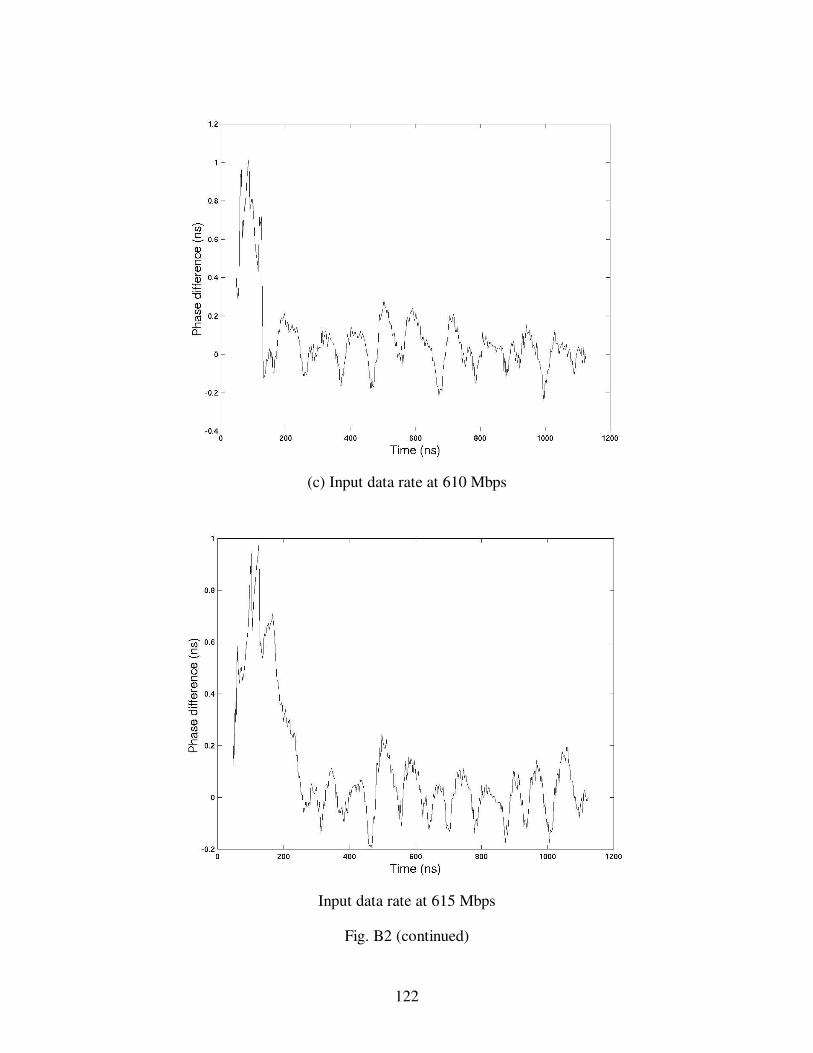
122
(c) Input data rate at 610 Mbps
Input data rate at 615 Mbps
Fig. B2 (continued)
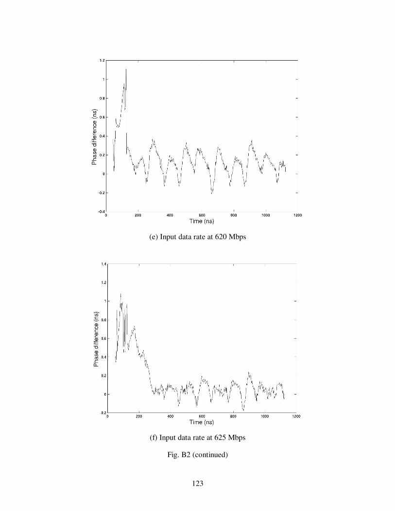
123
(e) Input data rate at 620 Mbps
(f) Input data rate at 625 Mbps
Fig. B2 (continued)

124
(g) Input data rate at 630 Mbps
(h) Input data rate at 635 Mbps
Fig. B2 (continued)
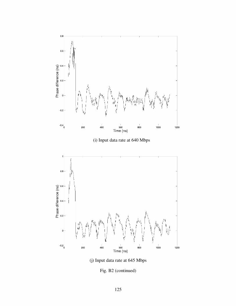
125
(i) Input data rate at 640 Mbps
(j) Input data rate at 645 Mbps
Fig. B2 (continued)
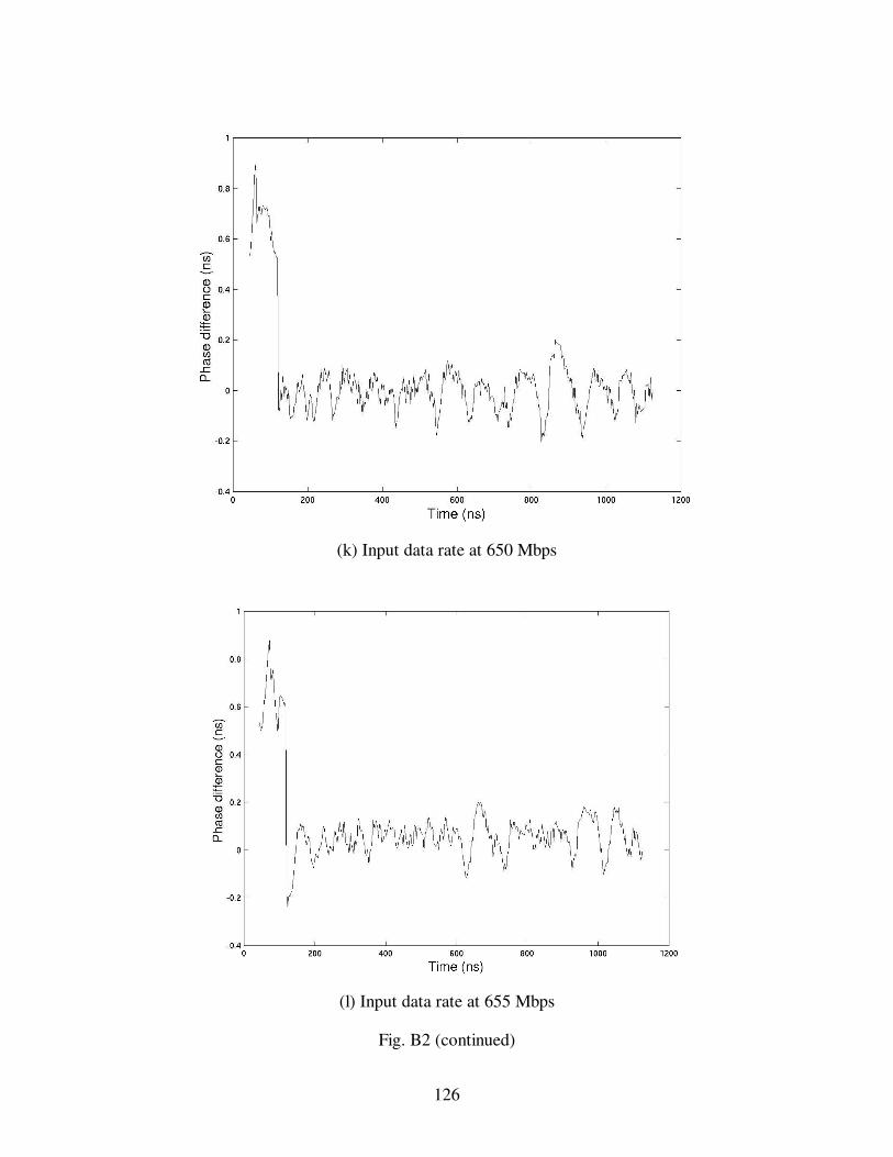
126
(k) Input data rate at 650 Mbps
(l) Input data rate at 655 Mbps
Fig. B2 (continued)

127
(m) Input data rate at 660 Mbps
(n) Input data rate at 665 Mbps
Fig. B2 (continued)
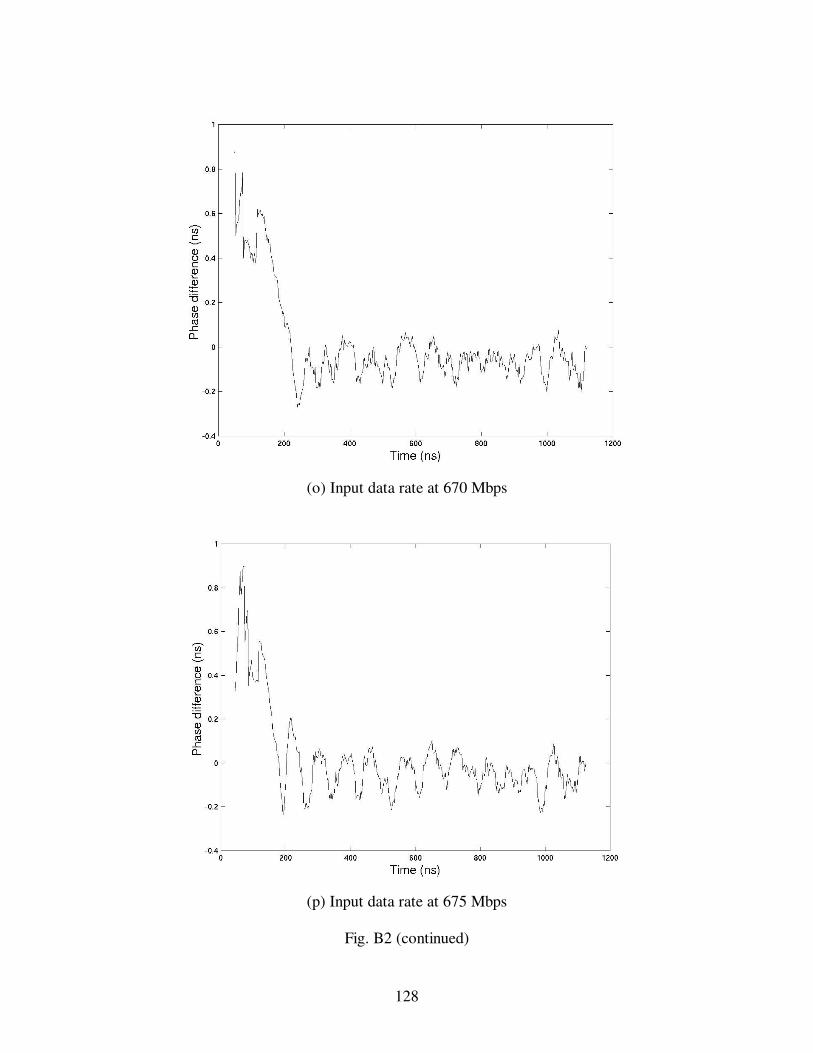
128
(o) Input data rate at 670 Mbps
(p) Input data rate at 675 Mbps
Fig. B2 (continued)

129
(q) Input data rate at 680 Mbps
(r) Input data rate at 685 Mbps
Fig. B2 (continued)
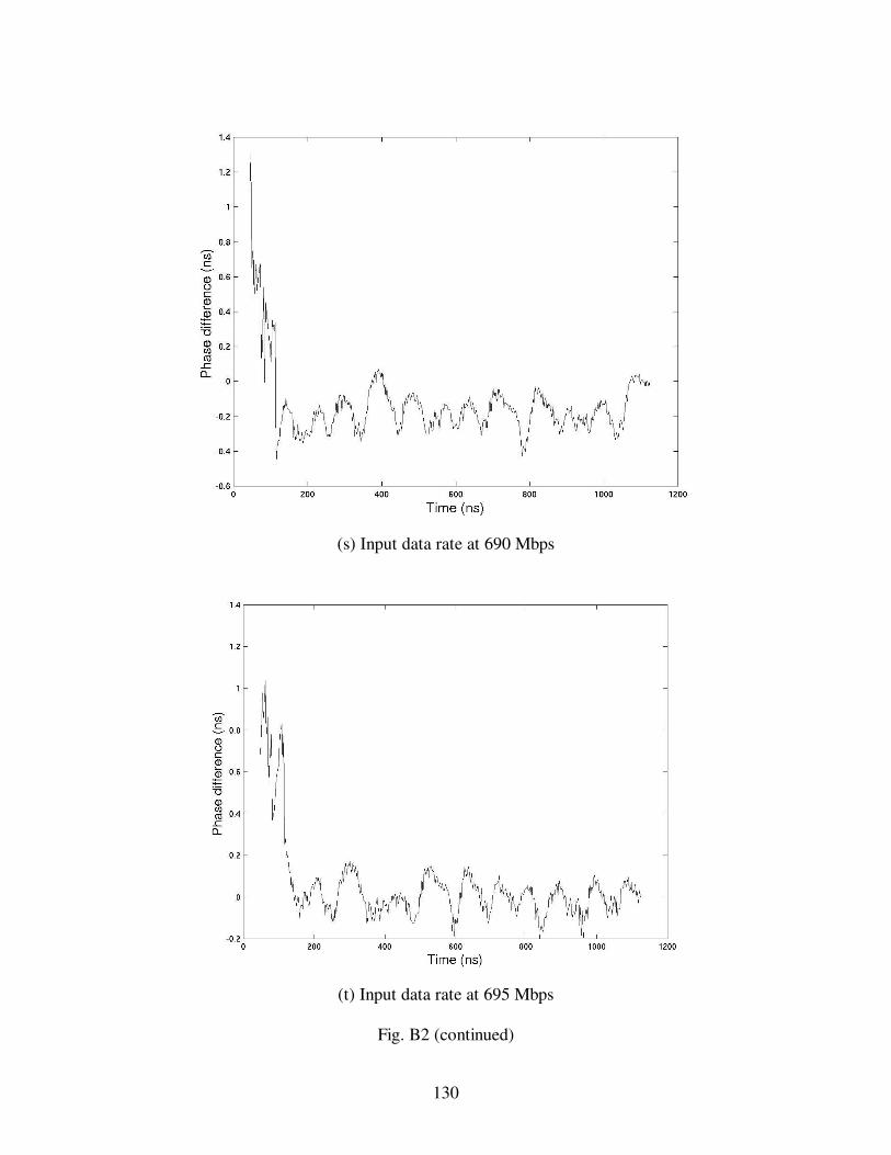
130
(s) Input data rate at 690 Mbps
(t) Input data rate at 695 Mbps
Fig. B2 (continued)
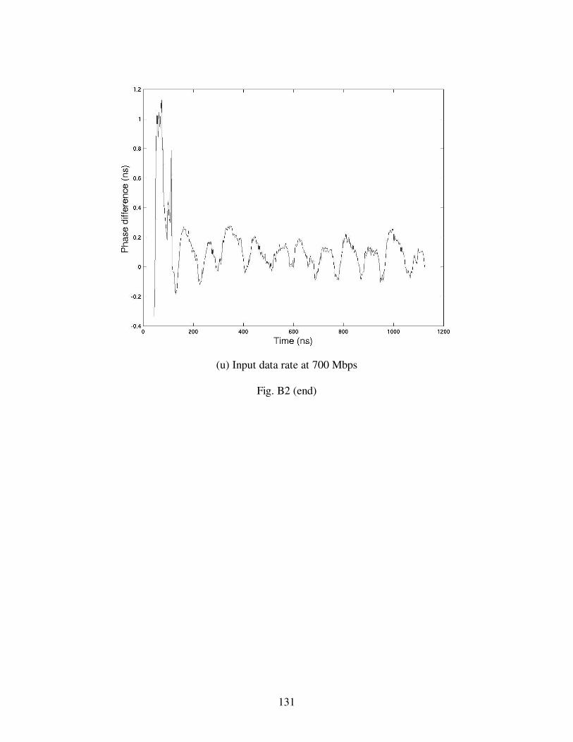
131
(u) Input data rate at 700 Mbps
Fig. B2 (end)