Embed Size (px)
Citation preview

Best USB Audio I/O Controller for External High End 8CH Audio Devices
CM106-F/L High Integrated USB Audio I/O Controller
DataSheet 1.3
C-MEDIA ELECTRONICS INC. TEL: 886-2-8773-1100 FAX: 886-2-8773-2211
6F, 100, Sec. 4, Civil Boulevard, Taipei, Taiwan 106, R.O.C. For detailed product information, please contact [email protected]

CM106-F/L
High End 8CH DAC and 2CH ADC Integrated Solution
Date: 09/01/2004 Version: 1.3- 2 -
NOTICES THIS DOCUMENT IS PROVIDED “AS IS” WITH NO WARRANTIES WHAT SO EVER, INCLUDING ANY WARRANTY OF MERCHANT ABILITY, NONINFRINGEMENT, FITNESS FOR ANY PARTICULAR PURPOSE, OR ANY WARRANTY OTHERWISE ARISING OUT OF ANY PROPOSAL, DOCUMENT OR SAMPLE.
ALL RIGHTS RESERVED. NO PART OF THIS DOCUMENT MAY BE REPRODUCED OR TRANSMITTED IN ANY FORM OR BY ANY MEANS, ELECTRONIC OR MECHANICAL, INCLUDING INFORMATION STORAGE AND RETRIEVAL SYSTEMS, WITHOUT PERMISSION IN WRITING FROM C-MEDIA ELECTRONICS, INC.
COPYRIGHT
Copyright (c) 2003-2004 C-Media Electronics Inc.
All rights reserved. All content included on this document, such as text, graphics, logos, button icons, images, audio clips, digital downloads, data compilations, and software, is either the exclusive property of C-Media Electronics Inc., its affiliates (collectively, "C-Media"), its content suppliers, or its licensors and protected by Republic of China and international copyright laws.
TRADEMARKS
C-Media, the C-Media Logo, Xear 3D, Xear 3D Logo, Speaker Shifter, Smart Jack, and Smart Audio Jack are trademarks of C-Media Electronics Inc. in Republic of China and/or other countries. All other brand and product names listed are trademarks or registered trademarks of their respective holders and are hereby recognized as such.
*C-Media reserves the right to modify the specifications without further notice*

CM106-F/L
High End 8CH DAC and 2CH ADC Integrated Solution
Date: 09/01/2004 Version: 1.3- 3 -
Table of Contents 1. Description and Overview 2. Features 3. Pin Descriptions 3.1 CM106-F QFP 100 Pin Table 3.2 CM106-L LQFP 48 Pin Table 3.3 CM106-F QFP 100 Pin 3.4 CM106-L LQFP 48 Pin 4. Ordering Information 5. Function Block Diagram of CM106-F/L 6. Function Descriptions 6.1 Internal Register 6.2 MCU Interface 6.3 Serial EEPROM Content 6.4 DAC 6.5 ADC 6.6 Power Management 7. Volume Control 7.1 DAC Volume Control 7.2 ADC Volume Control 7.3 MIC / LINE-IN Monitor Volume Control 8. Electrical Characteristics 8.1 Absolute Maximum Rating 8.2 Recommended Operation Conditions 8.3 Audio Performance 9. Audio Performance Curves 9.1 AA path (Line In to Line Out) Frequency Response 9.2 AA path (Line In to Line Out) Cross Talk 9.3 DAC (Front) Frequency Response @ 48ks/sec 9.4 DAC (Front) Frequency Response @ 44.1ks/sec 9.5 DAC (Front) Pass Band Ripple @ 48ks/sec 9.6 DAC (Front) Pass Band Ripple @ 44.1ks/sec 9.7 ADC (Line In) Frequency Response @ 48ks/sec 9.8 ADC (Mic In) Frequency Response @ 48ks/sec

CM106-F/L
High End 8CH DAC and 2CH ADC Integrated Solution
Date: 09/01/2004 Version: 1.3- 4 -
10. Application Circuit 10.1 CM106-L (LQFP 48) / CM106-F (QFP 100)

CM106-F/L
High End 8CH DAC and 2CH ADC Integrated Solution
Date: 09/01/2004 Version: 1.3- 5 -
1. Description and Overview CM106-F/L is a highly integrated single chip USB audio solution. All essential analog modules are embedded in CM106, including 8CH DAC and earphone buffer, 2CH ADC, microphone booster, PLL, regulator, and USB transceiver. It is very suitable for high end USB external audio box, USB multi-channel headphone or USB audio interface multi-channel speaker set application. Many features are programmable with external EEPROM and MCU interface. In addition, MCU/EEPROM/GPIO control can easily via HID software interface. Better yet, CM106-F/L support stereo MIC, phone jack sense, S/PDIF I/O and 48/44.1 Khz sampling rate. Moreover, unique patent driver can support world first SPEAKER SHIFTER, full HRTF 3D, EAX2.0, Karaoke and Dolby AC-3 real-time encoder function.
2. Features
USB spec. 2.0 full speed compliant USB audio device class spec. 1.0 and USB HID class spec. 1.1 compliant IEC60958 spec. compliant (consumer format S/PDIF input and output with
loop-back support) SCMS (Serial Copy Management System) compliant Dolby® digital audio streaming via S/PDIF out USB remote wake-up support 8 channel DAC output with
16 bit resolution 3.1 Vpp (1.1 Vrms) biased at 2.25V output swing Volume control and mute function Earphone buffer 2X interpolator for digital playback data to improve quality
2 channel ADC input with 16 bit resolution 3.2 Vpp (or 4.0 Vpp programmed by vendor driver) biased at 2.25V input swing Volume control and mute function
Additional headphone output with selectable source and phone jack sense

CM106-F/L
High End 8CH DAC and 2CH ADC Integrated Solution
Date: 09/01/2004 Version: 1.3- 6 -
Stereo MIC support with boost capability Recording source select from S/PDIF, MIC, Line-in and summation of MIC, Line-in
and front channel MIC, Line-in monitor from front channel (all channels optional) with volume control
and mute function Master volume control by default; per-channel volume control by C-Media driver Playback with soft-mute function Support 48 / 44.1 KHz sampling rate for both playback and recording MCU support with two-wire serial interface Serial EEPROM support for customized VID/PID MCU / EEPROM / GPIO control via HID software interface Volume up / volume down / playback mute HID button LED indicator pins: operation / recording mute / SCMS protection C-Media value added software (multi-channel positional 3D sound, AC-3 encoder,
etc.) Embedded USB transceiver and power on reset circuit Single 12MHz crystal input with embedded PLL Single 5V power supply with embedded 5V to 3.3V regulator Industry standard LQFP-48 (CM106-L) or QFP-100 (CM106-F) package C-Media value added patent software driver
Xear 3D sound Earphone Plus SPEAKER SHIFTER Environment sound effects Room Size Mode Graphic Equalizer Karaoke Function Dolby Digital Real-Time Content Encoder (Optional)

CM106-F/L
High End 8CH DAC and 2CH ADC Integrated Solution
Date: 09/01/2004 Version: 1.3- 7 -
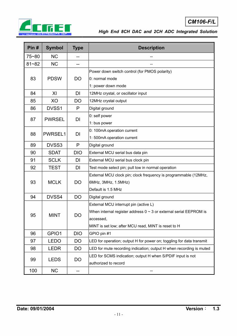
3. Pin Descriptions
3.1 CM106-F QFP 100Pin Table
PIN # Signal Name PIN # Signal Name PIN # Signal Name PIN # Signal Name1~7 NC 31~34 NC 61 LOCF 85 XO
8 DVSS5 35 LIL 62 LOLFE 86 DVSS1 9 PHONES 36 LIR 63 AVSS2 87 PWRSEL
10 CS 37 AVDD1 64 DVSS6 88 PWRSEL1 11 SK 38 VREF 65 VOLUP 89 DVSS3 12 DR 39 VBIAS 66 VOLDN 90 SDAT 13 DW 40 AVSS1 67 SPDIFI 91 SCLK 14 MSEL1 41 HPOUTL 68 MUTER 92 TEST 15 MSEL2 42 HPOUTR 69 MUTEP 93 MCLK 16 DVSS2 43 LOSL 70 SPDIFO 94 DVSS4 17 USBDP 44 LOSR 71 GPIO2 95 MINT 18 USBDM 45 LOFL 72 GPIO3 96 GPIO1 19 REGV 46 LOFR 73 GPIO4 97 LEDO 20 DVDD1 47~50 NC 74 DVSS7 98 LEDR 21 AVSS3 51~57 NC 75~80 NC 99 LEDS 22 MICINL 58 AVDD2 81~82 NC 100 NC 23 MICINR 59 LOLS 83 PDSW
24~30 NC 60 LORS 84 XI
3.2 CM106-L LQFP 48Pin Table
PIN # Signal Name PIN # Signal Name PIN # Signal Name1 PDSW 17 DW 33 LOSL 2 XI 18 USBDP 34 LOSR 3 XO 19 USBDM 35 LOFL 4 DVSS1 20 REGV 36 LOFR 5 SDAT 21 DVDD1 37 AVDD2 6 SCLK 22 AVSS3 38 LOLS 7 TEST 23 MICINL 39 LORS 8 MCLK 24 MICINR 40 LOCF 9 MINT 25 LIL 41 LOLFE
10 GPIO1 26 LIR 42 AVSS2 11 LEDO 27 AVDD1 43 VOLUP 12 LEDR 28 VREF 44 VOLDN 13 PHONES 29 VBIAS 45 SPDIFI 14 CS 30 AVSS1 46 MUTER 15 SK 31 HPOUTL 47 MUTEP 16 DR 32 HPOUTR 48 SPDIFO

CM106-F/L
High End 8CH DAC and 2CH ADC Integrated Solution
Date: 09/01/2004 Version: 1.3- 8 -
Figure 1. CM106-F QFP 100 Pin Assignments (Top View)
Figure 2. CM106-L LQFP 48 Pin Assignments (Top View)

CM106-F/L
High End 8CH DAC and 2CH ADC Integrated Solution
Date: 09/01/2004 Version: 1.3- 9 -
3.3 CM106-F QFP 100 PIN
Pin # Symbol Type Description
1~7 NC -- -- 8 DVSS5 P Digital ground
9 PHONES DI Phone jack sense pin for line out Tri-state; an internal register bit will be
set when activated (active H)
10 CS DO EEPROM interface chip select
11 SK DO EEPROM interface clock
12 DR DO EEPROM interface data read
13 DW DI EEPROM interface data write
14 MSEL1 DI 0: MICINL/R and LIL/R mix to 8 channels
1: MICINL/R and LIL/R mix to LOFL and LOFR
15 MSEL2 DI 0: playback only
1: playback and recording
16 DVSS2 P Digital ground
17 USBDP AIO USB data D+
18 USBDM AIO USB data D-
19 REGV AO 3.3V reference output for internal 5 3.3V regulator
20 DVDD1 P 5V power supply to internal regulator
21 AVSS3 P Analog ground
22 MICINL AI Microphone input left channel
23 MICINR AI Microphone input right channel
24~30 NC -- --
31~34 NC -- --
35 LIL AI Line-In input left channel
36 LIR AI Line-In input right channel
37 AVDD1 P 5V analog power for analog circuit
38 VREF AO Connecting to external decoupling capacitor for embedded band-gap
circuit; 2.25V output

CM106-F/L
High End 8CH DAC and 2CH ADC Integrated Solution
Date: 09/01/2004 Version: 1.3- 10 -
Pin # Symbol Type Description
39 VBIAS AO Microphone bias voltage supply (4.5V/2.25V)
40 AVSS1 P Analog ground
41 HPOUTL AO Headphone out left channel
42 HPOUTR AO Headphone out right channel
43 LOSL AO Line out side (back) left channel
44 LOSR AO Line out side (back) right channel
45 LOFL AO Line out front left channel
46 LOFR AO Line out front right channel
47~50 NC -- --
51~57 NC -- --
58 AVDD2 P 5V analog power for analog circuit
59 LOLS AO Line out surround (rear) left channel
60 LORS AO Line out surround (rear) right channel
61 LOCF AO Line out center channel
62 LOLFE AO Line out LFE (subwoofer) channel
63 AVSS2 P Analog ground
64 DVSS6 P Digital ground
65 VOLUP DI Volume up (edge trigger with de-bouncing)
66 VOLDN DI Volume down (edge trigger with de-bouncing)
67 SPDIFI DI S/PDIF input
68 MUTER DI Mute recording (edge trigger with de-bouncing)
69 MUTEP DI Mute playback (edge trigger with de-bouncing)
70 SPDIFO DO S/PDIF output
71 GPIO2 DIO GPIO pin #2
72 GPIO3 DIO GPIO pin #3
73 GPIO4 DIO GPIO pin #4
74 DVSS7 P Digital ground
CM106-F/L
High End 8CH DAC and 2CH ADC Integrated Solution
Date: 09/01/2004 Version: 1.3- 11 -
Pin # Symbol Type Description
75~80 NC -- --
81~82 NC -- --
83 PDSW DO Power down switch control (for PMOS polarity)
0: normal mode
1: power down mode
84 XI DI 12MHz crystal, or oscillator input
85 XO DO 12MHz crystal output
86 DVSS1 P Digital ground
87 PWRSEL DI 0: self power
1: bus power
88 PWRSEL1 DI 0: 100mA operation current
1: 500mA operation current
89 DVSS3 P Digital ground
90 SDAT DIO External MCU serial bus data pin
91 SCLK DI External MCU serial bus clock pin
92 TEST DI Test mode select pin; pull low in normal operation
93 MCLK DO External MCU clock pin; clock frequency is programmable (12MHz,
6MHz, 3MHz, 1.5MHz)
Default is 1.5 MHz
94 DVSS4 DO Digital ground
95 MINT DO
External MCU interrupt pin (active L)
When internal register address 0 ~ 3 or external serial EEPROM is
accessed,
MINT is set low; after MCU read, MINT is reset to H
96 GPIO1 DIO GPIO pin #1
97 LEDO DO LED for operation; output H for power on; toggling for data transmit
98 LEDR DO LED for mute recording indication; output H when recording is muted
99 LEDS DO LED for SCMS indication; output H when S/PDIF input is not
authorized to record
100 NC -- --

CM106-F/L
High End 8CH DAC and 2CH ADC Integrated Solution
Date: 09/01/2004 Version: 1.3- 12 -
3.4 CM106-L LQFP 48 PIN
Pin # Symbol Type Description
1 PDSW DO Power down switch control (for PMOS polarity)
0: normal mode
1: power down mode
2 XI DI 12MHz crystal, or oscillator input
3 XO DO 12MHz crystal output
4 DVSS1 P Digital ground
5 SDAT DIO External MCU serial bus data pin
6 SCLK DI External MCU serial bus clock pin
7 TEST DI Test mode select pin; pull low in normal operation
8 MCLK DO External MCU clock pin; clock frequency is programmable
(12MHz, 6MHz, 3MHz, 1.5MHz)
Default is 1.5 MHz
9 MINT DO
External MCU interrupt pin (active L)
When internal register address 0 ~ 3 or external serial EEPROM is
accessed,
MINT is set low; after MCU read, MINT is reset to H
10 GPIO1 DIO GPIO pin #1
11 LEDO DO LED for operation; output H for power on; toggling for data transmit
12 LEDR DO LED for mute recording indication; output H when recording is muted
13 PHONES DI Phone jack sense pin for line out Tri-state; an internal register bit will be
set when activated (active H)
14 CS DO EEPROM interface chip select
15 SK DO EEPROM interface clock
16 DR DO EEPROM interface data read
17 DW DI EEPROM interface data write
18 USBDP AIO USB data D+
19 USBDM AIO USB data D-
20 REGV AO 3.3V reference output for internal 5 3.3V regulator
21 DVDD1 P 5V power supply to internal regulator
22 AVSS3 P Analog ground
23 MICINL AI Microphone input left channel

CM106-F/L
High End 8CH DAC and 2CH ADC Integrated Solution
Date: 09/01/2004 Version: 1.3- 13 -
Pin # Symbol Type Description
24 MICINR AI Microphone input right channel
25 LIL AI Line-In input left channel
26 LIR AI Line-In input right channel
27 AVDD1 P 5V analog power for analog circuit
28 VREF AO Connecting to external decoupling capacitor for embedded band-gap
circuit; 2.25V output
29 VBIAS AO Microphone bias voltage supply (4.5V/2.25V)
30 AVSS1 P Analog ground
31 HPOUTL AO Headphone out left channel
32 HPOUTR AO Headphone out right channel
33 LOSL AO Line out side (back) left channel
34 LOSR AO Line out side (back) right channel
35 LOFL AO Line out front left channel
36 LOFR AO Line out front right channel
37 AVDD2 P 5V analog power for analog circuit
38 LOLS AO Line out surround (rear) left channel
39 LORS AO Line out surround (rear) right channel
40 LOCF AO Line out center channel
41 LOLFE AO Line out LFE (subwoofer) channel
42 AVSS2 P Analog ground
43 VOLUP DI Volume up (edge trigger with de-bouncing)
44 VOLDN DI Volume down (edge trigger with de-bouncing)
45 SPDIFI DI S/PDIF input
46 MUTER DI Mute recording (edge trigger with de-bouncing)
47 MUTEP DI Mute playback (edge trigger with de-bouncing)
48 SPDIFO DO S/PDIF output

CM106-F/L
High End 8CH DAC and 2CH ADC Integrated Solution
Date: 09/01/2004 Version: 1.3- 14 -
*Note 1: DI – digital input pad DO – digital output pad DIO – digital bi-directional pad AI/AO/AIO – analog pad P – power pad
*Note 2: For LQFP 48 package, PWRSEL, PWRSEL1, MSEL1 and MSEL2 are internal bonding options; They are not bonded by default.

CM106-F/L
High End 8CH DAC and 2CH ADC Integrated Solution
Date: 09/01/2004 Version: 1.3- 15 -
4. Ordering Information 4.1 CM106-L (LQFP48)

CM106-F/L
High End 8CH DAC and 2CH ADC Integrated Solution
Date: 09/01/2004 Version: 1.3- 16 -
4.2 CM106-F (QFP100)

CM106-F/L
High End 8CH DAC and 2CH ADC Integrated Solution
Date: 09/01/2004 Version: 1.3- 17 -
5. Function Block Diagram of CM106-F/L
Figure 3:Function Block Diagram Of CM106-F/L Signal Set Signals EEPROM CS, SK, DR, DW VOL I/F VOLUP, VOLDN, MUTER, MUTEP LED I/F LEDO, LEDR, LEDS MCU I/F SCLK, SDAT, MCLK, MINT
SEL PWRSEL, PWRSEL1, MSEL1, MSEL2 GPIO GPIO1, GPIO2, GPIO3, GPIO4 Power AVDD1, AVDD2, AVSS1, AVSS2, DVDD1, DVSS1, DVSS2

CM106-F/L
High End 8CH DAC and 2CH ADC Integrated Solution
Date: 09/01/2004 Version: 1.3- 18 -
6. Function Descriptions Block Diagram of CM106-F/L 6.1 Internal Register The internal registers of CM106 can be divided to two parts. Some of them (REG0, REG1, REG2 and REG3) are 16-bit width and can be accessed via HID interface. The others are 8-bit width and can be accessed by vendor requests. To access registers via HID interface, users should issue a “Set Output Report” HID request. The four bytes of output report data is organized as below:
Byte [0] Read: 8’d48
Write: 8’d32
Byte [1] DATAL
Byte [2] DATAH
Byte [3] Register address (0, 1, 2, 3)
In addition to internal registers, users can also access external serial EEPROM by the same way:
Byte [0] Read: 8’d80
Write: 8’d64
Byte [1] DATAL
Byte [2] DATAH
Byte [3] EEPROM address (0 ~ 8’d63)
When users intend to read register / EEPROM by “Set Output Report”, the returned data will be transferred to USB host via HID input report through interrupt pipe. The three bytes of input report data is organized as below:
Byte [0] MCUIN EEIN REGIN HEADPON MUTE VDN VUP
Byte [1]
DATAL from MCU when MCUIN = 1
DATAL from EEPROM when EEIN = 1
DATAL from Register when REGIN = 1
Byte [2]
DATAH from MCU when MCUIN = 1
DATAH from EEPROM when EEIN = 1
DATAH from Register when REGIN = 1

CM106-F/L
High End 8CH DAC and 2CH ADC Integrated Solution
Date: 09/01/2004 Version: 1.3- 19 -
Users can distinguish the source of input report by Byte[0], Byte[1] and Byte[2] consist a word which may be the content of addressed register or serial EEPROM. It may also be an arbitrary word programmed by external MCU. In addition, Byte[0] carries the information of HID button status (MUTE, VDN and VUP), and phone jack sense (HEADPON). VDN/VUP would be 1 when VOLDN/VOLUP button is pressed, and keeps pressed (VOLDN/VOLUP keeps 0). MUTE would be 1 when MUTEP button is pressed, and would be cleared to 0 after USB host reads the input report. HEADPON would be 1 when headphone is plugged in (PHONES is 1). Refer to the following tables for the definition of internal registers can be accessed via HID interface:
Address: 0x00 REG0 Reset State: 0x0000
15 14 13 12 11 10 9 8 7 6 5 4 3 2 1 0
CSR
Bit
Number Bit
Mnemonic Read/ Write Function
12-0 CSR R/W SPDIF out control
Address: 0x01 REG1 Reset State: 0xb000
15 14 13 12 11 10 9 8
DACX2en FS PLLBINen
SOFTMUTEen GPIO4_o GPIO4_
OEN GPIO3_o GPIO3_OEN
7 6 5 4 3 2 1 0
GPIO2_o GPIO2_OEN GPIO1_o GPIO1_
OEN LOWFIR
SET SPDIFLO
OP DIS_SPD
IFO SPDIFMI
X
Bit Number
Bit Mnemonic
Read/Write Function
15 DACX2en R/W DAC X 2 enable 14 FS R/W ADC full scale setting 13 PLLBINen R/W PLL binary search enable 12 SOFTMUTEen R/W Soft mute enable 11 GPIO4_o R/W Gpio4 signal

CM106-F/L
High End 8CH DAC and 2CH ADC Integrated Solution
Date: 09/01/2004 Version: 1.3- 20 -
10 GPIO4_OEN R/W Gpio4 output enable 9 GPIO3_o R/W Gpio3 signal 8 GPIO3_OEN R/W Gpio3 output enable 7 GPIO2_o R/W Gpio2 signal 6 GPIO2_OEN R/W Gpio2 output enable 5 GPIO1_o R/W Gpio1 signal 4 GPIO1_OEN R/W Gpio1 output enable 3 LOWFIRSET R/W Low pass filter setting 2 SPDIFLOOP R/W SPDIF loop-back enable 1 DIS_SPDIFO R/W SPDIF out disable 0 SPDIFMIX R/W SPDIF in mix enable
Address: 0x02 REG2 Reset State: 0x0004
15 14 13 12 11 10 9 8 DRIVERON HEADPSEL PLAYMUTE
7 6 5 4 3 2 1 0
PLAYMUTE MICRSEL MCUCLKSEL
Bit Number
Bit Mnemonic
Read/ Write Function
15 DRIVERON R/W If (HEADPON = 1 and DRIVERON = 0) 1. All channels muted except Headphone channels2. Select Headphone source from Front channels
Else 1. Channel mute controlled by PLAYMUTE
registers 2. Headphone source selected by HEADPSEL
registers 14~13 HEADPSEL R/W Headphone source select
00: Front channels 01: Center and Subwoofer 02: Surround channels 03: Side channels
12~3 PLAYMUTE R/W Channel mute control (high active) PLAYMUTE[0]: mute Left Front PLAYMUTE[1]: mute Right Front PLAYMUTE[2]: mute Center PLAYMUTE[3]: mute Subwoofer PLAYMUTE[4]: mute Left Surround PLAYMUTE[5]: mute Right Surround PLAYMUTE[6]: mute Side Left PLAYMUTE[7]: mute Side Right PLAYMUTE[8]: mute Headphone Left PLAYMUTE[9]: mute Headphone Right

CM106-F/L
High End 8CH DAC and 2CH ADC Integrated Solution
Date: 09/01/2004 Version: 1.3- 21 -
2 MICRSEL R/W MIC right channel source select 0: left channel (mono) 1: right channel (stereo)
1~0 MCUCLKSEL R/W MCU clock frequency 00: 1.5Mhz 01: 3Mhz 10: 6Mhz 11: 12Mhz
Address: 0x03 REG3 Reset State: 0x003f / 0x007f
15 14 13 12 11 10 9 8 VRAP
25EN MSEL1 SPDFI_
FREQ[1]
7 6 5 4 3 2 1 0 SPDFI
_FREQ[0] PINSEL FOE ROE CBOE LOSE HPOE CANREC
Bit Number
Bit Mnemonic
Read/Write
Function
10 VRAP25EN R/W Microphone bias voltage supply select 0: 4.5V 1: 2.25V
9 MSEL1 R/W 0: MICINL/R and LIL/R mix to LOFL and LOFR 1: MICINL/R and LIL/R mix to 8 channels
8~7 SPDFI_FREQ R SPDIF in sample rate 00: 44.1K 01: reserved 10: 48K 11: 32K
6 PINSEL R 0: 100 pin package 1: 48 pin package
5 FOE R/W 1: LOFL/LOFR enable 0: LOFL/LOFR disable (Hi Z)
4 ROE R/W 1: LOLS/LORS enable 0: LOLS/LORS disable (Hi Z)
3 CBOE R/W 1: LOCF/LOLFE enable 0: LOCF/LOLFE disable (Hi Z)
2 LOSE R/W 1: LOSL/LOSR enable 0: LOSL/LOSR disable (Hi Z)
1 HPOE R/W 1: HPOUTL/HPOUTR enable 0: HPOUTL/HPOUTR disable (Hi Z)
0 CANREC R SPDIF in recording status 0: SPDIF in can not be recorded 1: SPDIF in can be recorded

CM106-F/L
High End 8CH DAC and 2CH ADC Integrated Solution
Date: 09/01/2004 Version: 1.3- 22 -
6.2 MCU Interface CM106 can communicate with external MCU via two-wire serial interface and act as a slave device. By this way, MCU can read four bytes from and write two bytes to USB host through CM106. When MCU writes two bytes to CM106, the data will be transferred to USB host via HID ‘Input Report’. USB host will keep polling HID report every 32ms. CM106 can also transfer four bytes from USB host to MCU. This is accomplished by a ‘Set Output Report’ HID request issued by USB host. CM106 will then assert MINT to inform MCU to read them. CM106 has one input pin ‘SCLK’ to get serial clock from MCU, and one open-drain output pin ‘SDAT’ to send or receive serial signal to/from MCU. As shown below, ‘SDAT’ should be stable when ‘SCLK’ is high, and can have transition only when ‘SCLK’ is low.
START and STOP conditions shown below are the exception. Every transaction begins from a START, and ends with a STOP, or another START (repeated START).
The figure below demonstrates a transaction example. After every 8 bits sent by the transmitter, the receiver should send one bit low for positive acknowledgement or one bit high for negative acknowledgement. After the negative acknowledgement, a STOP or repeated START should follow.

CM106-F/L
High End 8CH DAC and 2CH ADC Integrated Solution
Date: 09/01/2004 Version: 1.3- 23 -
The figure below shows typical transactions between MCU and CM106. After a START, MCU should send 7-bit slave address (7’b0111000) first, and then the 8th bit denotes a read transfer when it’s high; or a write transfer when it’s low. MCU write:
S 8’h70 0 8’h01 0 Byte[1] 0 Byte[2] 1 P MCU read:
S 8’h70 0 8’h00 1 S 8’h71 0 Byte[0] 0 Byte[1] 0 Byte[2] 0 Byte[3] 1 P
: From CM106 to MCU : From MCU to CM106
S : START condition P : STOP condition
0 : Positive acknowledge 1 : Negative acknowledge Byte : One byte data
In a write transfer, MCU keeps acting as the transmitter. CM106 regards the first DATA byte as start register address. The second and third DATA bytes are the content that MCU writes to the register addresses. In a read transfer, two transactions are necessary. MCU resets start register address by the first transaction. Then MCU changes to be the receiver during the second transaction to get four bytes of data.

CM106-F/L
High End 8CH DAC and 2CH ADC Integrated Solution
Date: 09/01/2004 Version: 1.3- 24 -
6.3 Serial EEPROM Content CM106 supports four-wire serial EEPROM interface. When an external serial EEPROM is detected, Vendor ID and Product ID reported within Device Descriptor will be derived from the content of serial EEPROM. The organization of serial EEPROM is shown below:
Address = 0 16’h630X Address = 1 Vendor ID Address = 2 Product ID Address = 63 16’hXXXX
Users can program serial EEPROM via HID interface, as described in the former section. Although 64 words can be accessed by CM106, only the first three words are significant to CM106. The first word is a magic code. Only when it matches, CM106 will regard the serial EEPROM valid. 6.4 DAC CM106 contains eight 16-bit DACs. The DACs are implemented in two-stage resister ladder architecture. With 2X interpolator in logic block, these DACs are indeed operated at two time of sample rate. The playback stream from USB host is in signed 16-bit binary. CM106’s logic block converts the data to unsigned format, and adds 64 as a fixed offset. The converted data to DAC input is then in unsigned 17-bit binary. The 2X interpolator, and fixed offset value added upon playback stream could improve SNR. 6.5 ADC CM106 contain two 16-bit ADCs. The ADCs are implemented in Sigma-Delta architecture. In addition to the default digital low pass filter, CM106 provides an alternate one that could improve SNR further. A larger ADC input swing (4.0Vp-p) is also available. Refer to the internal register section for more information.

CM106-F/L
High End 8CH DAC and 2CH ADC Integrated Solution
Date: 09/01/2004 Version: 1.3- 25 -
6.6 Power Management To meet suspend current specification of USB, CM106 turns off most blocks when entering suspend. The only two exception are power-on-reset and regulator. To meet unconfigured current specification of USB, CM106 provides a control signal PDSW to turn off external components. PDSW would be active when USB host does not configure CM106. PDSW would also be active when CM106 is suspended. If serial EEPROM is exist, notice that it should not be powered off anyway because it contains Vendor ID and Product ID which should be returned to USB host before CM106 is configured. The value of two input pin PWRSEL and PWRSEL1 (for CM106-F only) would affect configuration descriptor. If users declare the device as bus-power and high-power, and it is attached to a bus-power hub, USB host would not configure the device because the power budget is over.

CM106-F/L
High End 8CH DAC and 2CH ADC Integrated Solution
Date: 09/01/2004 Version: 1.3- 26 -
7. Volume Control 7.1 DAC Volume Control
VOL_*_<5:0> Scale (linear) VOL_*_<5:0> Scale (linear) VOL_*_<5:0> Scale (linear) VOL_*_<5:0> Scale (linear)
00 1.000 10 0.724 20 0.448 30 0.171
01 0.973 11 0.696 21 0.420 31 0.144
02 0.944 12 0.669 22 0.392 32 0.116
03 0.917 13 0.641 23 0.365 33 0.088
04 0.890 14 0.613 24 0.337 34 0.061
05 0.862 15 0.586 25 0.309 35 0.033
06 0.834 16 0.558 26 0.282 36 0.006
07 0.807 17 0.530 27 0.254 37 mute
08 0.779 18 0.503 28 0.227
09 0.751 19 0.475 29 0.199 Note: VOL_*_ stands for VOL_FL_, VOL_FR_, VOL_CF_, VOL_LFE_, VOL_LS_, VOL_RS_, VOL_SL_, VOL_SR_. The volume control is in linear scale.
7.2 ADC Volume Control
VOL_*_<3:0> Scale (log) VOL_*_<3:0> Scale (log) VOL_*_<3:0> Scale (log) VOL_*_<3:0> Scale (log)
00 +22.5dB 04 +16.5dB 08 +10.5dB 12 +4.5dB
01 +21.0dB 05 +15.0dB 09 +9.0dB 13 +3.0dB
02 +19.5dB 06 +13.5dB 10 +7.5dB 14 +1.5dB
03 +18.0dB 07 +12.0dB 11 +6.0dB 15 0.0dB Note: VOL_*_ stands for VOL_REC_L_ and VOL_REC_R_. The volume control is in log scale.
7.3 MIC / Line-in Monitor Volume Control VOL_*_<4:0> Scale (log) VOL_*_<4:0> Scale (log) VOL_*_<4:0> Scale (log) VOL_*_<4:0> Scale (log)
00 +12.0dB 08 0.0dB 16 -12.0dB 24 -24.0dB
01 +10.5dB 09 -1.5dB 17 -13.5dB 25 -25.5dB
02 +9.0dB 10 -3.0dB 18 -15.0dB 26 -27.0dB
03 +7.5dB 11 -4.5dB 19 -16.5dB 27 -28.5dB
04 +6.0dB 12 -6.0dB 20 -18.0dB 28 -30.0dB
05 +4.5dB 13 -7.5dB 21 -19.5dB 29 -31.5dB
06 +3.0dB 14 -9.0dB 22 -21.0dB 30 -33.0dB
07 +1.5dB 15 -10.5dB 23 -22.5dB 31 mute Note: VOL_*_ stands for VOL_MICM_L_, VOL_MICM_R_, VOL_LINEM_L_, VOL_LINEM_R_. The volume control is in log scale.

CM106-F/L
High End 8CH DAC and 2CH ADC Integrated Solution
Date: 09/01/2004 Version: 1.3- 27 -
8. Electrical Characteristics 8.1 Absolute Maximum Rating
Symbol Parameter Value Unit
Dvmin Min Digital Supply Voltage – 0.3 V
Dvmax Max Digital Supply Voltage + 6 V
Avmin Min Analog Supply Voltage – 0.3 V
Avmax Max Analog Supply Voltage + 6 V
Dvinout Voltage on any Digital Input or Output
Pin
–0.3 to +5.5 V
Avinout Voltage on any Analog Input or Output
Pin
–0.3 to +5.5 V
TBstgB Storage Temperature Range -40 to +125 oC
ESD (HBM) ESD Human Body Mode 3500 V
ESD (MM) ESD Machine Mode 200 V
ILatch_Up Latch Up Trigger Current 400 mA
8.2 Recommended Operation Conditions
Operation conditions
Min Typ Max Unit
Analog Supply Voltage 4.5 5.0 5.5 V
Digital Supply Voltage 4.5 5.0 5.5 V
Operating Current: - - 350 mA
Un-configure Current 80 mA
Suspend Current - - 250 uA
Operating ambient temperature 0 - 70 P0PC
8.3 Audio Performance
Min Typ Max Unit
AA Path (Line In to Line Out)
THD + N (-3dBr) -89 dB
Dynamic range 99 dB
Cross talk 101 dB
Frequency response 48KHz 20 20K Hz

CM106-F/L
High End 8CH DAC and 2CH ADC Integrated Solution
Date: 09/01/2004 Version: 1.3- 28 -
DAC (Front)
THD + N (-3dBr) - -69 - dB
SNR - 92 - dB
Dynamic range 90 dB
Frequency response @ 48KHz 20 20K Hz
Frequency Response @ 44.1KHz 20 17.6K Hz
Full Scale Output Voltage Range - 1.17 - Vrms
Center Voltage 2.25 V
Pass Band Ripple @ 48KHz +-0.05 dB
Pass Band Ripple @ 44.1KHz +-0.05 dB
DAC (Rear)
THD + N (-3dBr) - -70 - dB
SNR - 91 - dB
Dynamic range 90 dB
DAC (Center/Bass)
THD + N (-3dBr) - -68 - dB
SNR - 91 - dB
Dynamic range 90 dB
DAC (Back Surround)
THD + N (-3dBr) - -68 - dB
SNR - 91 - dB
Dynamic range 90 dB
ADC (Line In)
THD + N (-3dBr) -70 dB
SNR 84 dB
Dynamic Range 85 dB
Frequency Response @ 48KHz 20 20K Hz
Input Range 0 - 3.2 (4.0) Vpp
ADC (Mic)
THD + N (-3dBr) -68 dB
SNR 83 dB
Dynamic Range 84 dB
Frequency Response @ 48KHz 70 12.5 Hz
Input Range 0 - 3.2 (4.0) Vpp
*Note: All specifications at +25oC, AVdd=DVdd=5V, 10k Ohm loading

CM106-F/L
High End 8CH DAC and 2CH ADC Integrated Solution
Date: 09/01/2004 Version: 1.3- 29 -
9. Audio Performance Curves 9.1 AA path (Line In to Line Out) Frequency Response
C-Media 08/12/04 10:44:41Analog Pass-Through (A-A) for Line Input to Line OutputFrequency Response
LL-FreqRes p.at2
ColorSweep Trace Line Style Thick Data Axis Com m ent
1 1 Cyan Solid 2 Anlr.Level A Left1 2 Yellow Solid 2 Anlr.Level B R ight
-21
-19
-20.75
-20.5
-20.25
-20
-19.75
-19.5
-19.25
dBr B
-21
-19
-20.75
-20.5
-20.25
-20
-19.75
-19.5
-19.25
dBr A
20 20k50 100 200 500 1k 2k 5k 10k
Hz
9.2 AA path (Line In to Line Out) Cross Talk
C-Media 08/12/04 15:20:08Analog to Analog Crosstalk
aa-axtalk.at2
ColorSweep Trace Line Style Thick Data Axis Com m ent
1 1 Green Solid 3 Anlr.Cros s talk Left1 2 Yellow Solid 3 Anlr.Cros s talk Left
Line In to Line Out(10k ohm s Load)0dBr = 0dBFS = 1.9 dBV
-125
+0
-100
-75
-50
-25
dB
20 20k50 100 200 500 1k 2k 5k 10k
Hz

CM106-F/L
High End 8CH DAC and 2CH ADC Integrated Solution
Date: 09/01/2004 Version: 1.3- 30 -
9.3 DAC (Front) Frequency Response @ 48ks/sec
C-Media 08/12/04 14:53:18Digital Playback (PC-D-A) for Line Output FrequencyResponse
WL-Multitone-48k.at2
ColorSweep Trace Line Style Thick Data Axis Com m ent
1 1 Green Solid 3 Fas ttes t.Ch.1 Am pl!Norm alize Left1 2 Yellow Solid 3 Fas ttes t.Ch.2 Am pl!Norm alize Left
-6
+1
-5
-4
-3
-2
-1
+0
dBr A
30 10k50 100 200 500 1k 2k 5k
Hz
9.4 DAC (Front) Frequency Response @ 44.1ks/sec
C-Media 08/12/04 14:54:41Digital Playback (PC-D-A) for Line Output FrequencyResponse
WL-Multitone-44k.at2
ColorSweep Trace Line Style Thick Data Axis Com m ent
1 1 Green Solid 3 Fas ttes t.Ch.1 Am pl!Norm alize Left1 2 Yellow Solid 3 Fas ttes t.Ch.2 Am pl!Norm alize Left
-6
+1
-5
-4
-3
-2
-1
+0
dBr A
20 10k50 100 200 500 1k 2k 5k
Hz

CM106-F/L
High End 8CH DAC and 2CH ADC Integrated Solution
Date: 09/01/2004 Version: 1.3- 31 -
9.5 DAC (Front) Pass Band Ripple @ 48ks/sec
C-Media 08/12/04 14:54:00Digital Playback (PC-D-A) for Line Output PassbandRipple @48ks/sec
WL-Pas s bandRipple-M48k.at2
ColorSweep Trace Line Style Thick Data Axis Com m ent
1 1 Green Solid 3 Fas ttes t.Ch.1 Am pl!Norm alize Left1 2 Yellow Solid 3 Fas ttes t.Ch.2 Am pl!Norm alize Left
-0.6
+0.4
-0.4
-0.2
+0
+0.2
dB
40 9k50 100 200 500 1k 2k 5k
Hz
9.6 DAC (Front) Pass Band Ripple @ 44.1ks/sec
C-Media 08/12/04 14:55:21Digital Playback (PC-D-A) for Line Output PassbandRipple @44.1ks/sec
WL-Pas s bandRipple-M44k.at2
ColorSweep Trace Line Style Thick Data Axis Com m ent
1 1 Green Solid 3 Fas ttes t.Ch.1 Am pl!Norm alize Left1 2 Yellow Solid 3 Fas ttes t.Ch.2 Am pl!Norm alize Left
-0.6
+0.4
-0.4
-0.2
+0
+0.2
dB
40 8k50 100 200 500 1k 2k 5k
Hz

CM106-F/L
High End 8CH DAC and 2CH ADC Integrated Solution
Date: 09/01/2004 Version: 1.3- 32 -
9.7 ADC (Line In) Frequency Response @ 48ks/sec
C-Media Digital Recording (A-D-PC) for Line Input Frequency Response
LW-MFreqRes p-48K.at2
ColorSweep Trace Line Style Thick Data Axis Com m ent
1 1 Green Solid 3 Fas ttes t.Ch.1 Am pl!Norm alize Left1 2 Yellow Solid 3 Fas ttes t.Ch.2 Am pl!Norm alize Left
-6
+1
-5
-4
-3
-2
-1
+0
dBr 1
20 10k50 100 200 500 1k 2k 5k
Hz
9.8 ADC (Mic In) Frequency Response @ 48ks/sec
C-Media Digital Recording (A-D-PC) for Line Input Frequency Response
LW-MFreqRes p-48K.at2
ColorSweep Trace Line Style Thick Data Axis Com m ent
1 1 Green Solid 3 Fas ttes t.Ch.1 Am pl!Norm alize Left1 2 Yellow Solid 3 Fas ttes t.Ch.2 Am pl!Norm alize Left
-6
+1
-5
-4
-3
-2
-1
+0
dBr 1
20 10k50 100 200 500 1k 2k 5k
Hz

CM106-F/L
High End 8CH DAC and 2CH ADC Integrated Solution
Date: 09/01/2004 Version: 1.3- 33 -
10. Application Circuit 10.1 CM106-L (LQFP48) / CM106-F (QFP100)

CM106-F/L
High End 8CH DAC and 2CH ADC Integrated Solution
Date: 09/01/2004 Version: 1.3- 34 -

CM106-F/L
High End 8CH DAC and 2CH ADC Integrated Solution
Date: 09/01/2004 Version: 1.3- 35 -
REFERENCE USB-IF, USB Specification, Revision 1.1 and 2.0, and USB Audio Device Class Specification, Revision 1.0,.
-End of Specifications-
C-MEDIA ELECTRONICS INC. 6F., 100, Sec. 4, Civil Boulevard, Taipei, Taiwan 106 R.O.C. TEL:886-2-8773-1100 FAX:886-2-8773-2211 E-mail:[email protected] URL:TUhttp://www.cmedia.com.twUT