Embed Size (px)
Citation preview
ECE 4420 – CMOS Technology (12/11/03) Page 1
Digital Integrated Circuit Design © P.E. Allen - 2003
CMOS TECHNOLOGYINTRODUCTION
Classification of Silicon Technology
Silicon IC Technologies
Bipolar Bipolar/CMOS MOS
JunctionIsolated
Dielectric Isolated
Oxideisolated
CMOSPMOS
(Aluminum Gate)
NMOS
Aluminum gate
Silicon gate
Aluminum gate
Silicon gate
Silicon-Germanium
Silicon 031211-01
ECE 4420 – CMOS Technology (12/11/03) Page 2
Digital Integrated Circuit Design © P.E. Allen - 2003
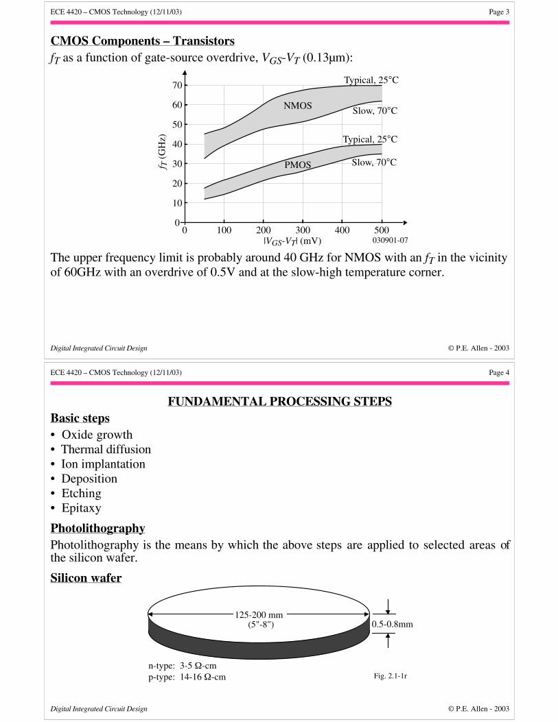
Components of a Modern CMOS TechnologyIllustration of a modern CMOS process:
n+
p-substrate
Metal Layers
NMOSTransistor
PMOSTransistor
031211-02
M1M2M3M4M5M6M7M80.8µm
0.3µm 7µm
Deep n-wellDeep p-well
n+
STIp+ p+
STI STI
Salicide
Polycide
Salicide
PolycideSidewall Spacers
Salicide
Source/drainextensions
Source/drainextensions
In addition to NMOS and PMOS transistors, the technology provides:1.) A deep n-well that can be utilized to reduce substrate noise coupling.2.) A MOS varactor that can serve in VCOs3.) At least 6 levels of metal that can form many useful structures such as inductors,
capacitors, and transmission lines.
ECE 4420 – CMOS Technology (12/11/03) Page 3
Digital Integrated Circuit Design © P.E. Allen - 2003
CMOS Components – TransistorsfT as a function of gate-source overdrive, VGS-VT (0.13µm):
100 200 300 400 500
20
30
40
50
60
70
10
00
Typical, 25°C
Slow, 70°CPMOS
Typical, 25°C
Slow, 70°CNMOS
f T (
GH
z)
|VGS-VT| (mV) 030901-07
The upper frequency limit is probably around 40 GHz for NMOS with an fT in the vicinityof 60GHz with an overdrive of 0.5V and at the slow-high temperature corner.
ECE 4420 – CMOS Technology (12/11/03) Page 4
Digital Integrated Circuit Design © P.E. Allen - 2003
FUNDAMENTAL PROCESSING STEPSBasic steps• Oxide growth• Thermal diffusion• Ion implantation• Deposition• Etching• Epitaxy
PhotolithographyPhotolithography is the means by which the above steps are applied to selected areas ofthe silicon wafer.
Silicon wafer
0.5-0.8mm
n-type: 3-5 Ω-cmp-type: 14-16 Ω-cm Fig. 2.1-1r
125-200 mm(5"-8")
ECE 4420 – CMOS Technology (12/11/03) Page 5
Digital Integrated Circuit Design © P.E. Allen - 2003
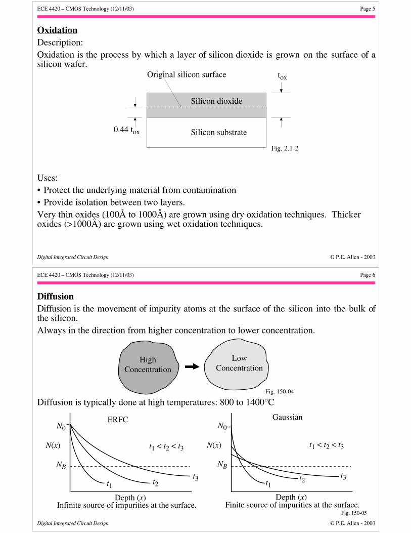
OxidationDescription:Oxidation is the process by which a layer of silicon dioxide is grown on the surface of asilicon wafer.
Original silicon surface
0.44 tox
tox
Silicon substrate
Silicon dioxide
Fig. 2.1-2
Uses:• Protect the underlying material from contamination• Provide isolation between two layers.Very thin oxides (100Å to 1000Å) are grown using dry oxidation techniques. Thickeroxides (>1000Å) are grown using wet oxidation techniques.
ECE 4420 – CMOS Technology (12/11/03) Page 6
Digital Integrated Circuit Design © P.E. Allen - 2003
DiffusionDiffusion is the movement of impurity atoms at the surface of the silicon into the bulk ofthe silicon. Always in the direction from higher concentration to lower concentration.
HighConcentration
LowConcentration
Fig. 150-04
Diffusion is typically done at high temperatures: 800 to 1400°C
Depth (x)
t1 < t2 < t3
t1t2
t3
N(x)
NB
Depth (x)
t1 < t2 < t3
Infinite source of impurities at the surface. Finite source of impurities at the surface.
N0
Fig. 150-05
ERFC Gaussian
t1 t2t3
N(x)
NB
N0
ECE 4420 – CMOS Technology (12/11/03) Page 7
Digital Integrated Circuit Design © P.E. Allen - 2003
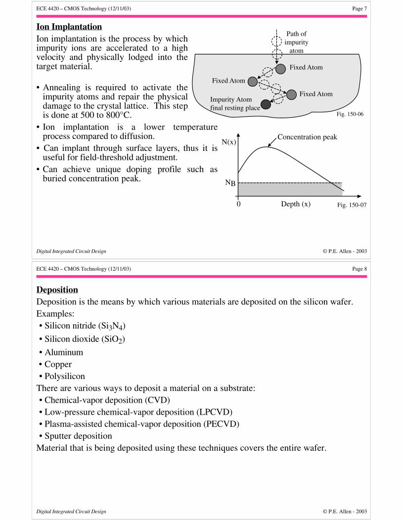
Ion ImplantationIon implantation is the process by whichimpurity ions are accelerated to a highvelocity and physically lodged into thetarget material.
• Annealing is required to activate theimpurity atoms and repair the physicaldamage to the crystal lattice. This stepis done at 500 to 800°C.
• Ion implantation is a lower temperatureprocess compared to diffusion.
• Can implant through surface layers, thus it isuseful for field-threshold adjustment.
• Can achieve unique doping profile such asburied concentration peak.
Path of impurity
atom
Fixed Atom
Fixed Atom
Fixed AtomImpurity Atomfinal resting place
Fig. 150-06
N(x)
NB
0 Depth (x)
Concentration peak
Fig. 150-07
ECE 4420 – CMOS Technology (12/11/03) Page 8
Digital Integrated Circuit Design © P.E. Allen - 2003
DepositionDeposition is the means by which various materials are deposited on the silicon wafer.Examples: • Silicon nitride (Si3N4)
• Silicon dioxide (SiO2)
• Aluminum • Copper • PolysiliconThere are various ways to deposit a material on a substrate: • Chemical-vapor deposition (CVD) • Low-pressure chemical-vapor deposition (LPCVD) • Plasma-assisted chemical-vapor deposition (PECVD) • Sputter depositionMaterial that is being deposited using these techniques covers the entire wafer.
ECE 4420 – CMOS Technology (12/11/03) Page 9
Digital Integrated Circuit Design © P.E. Allen - 2003
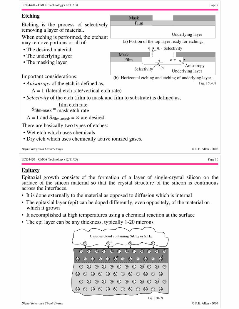
Etching
Etching is the process of selectivelyremoving a layer of material.When etching is performed, the etchantmay remove portions or all of: • The desired material • The underlying layer • The masking layer
Important considerations: • Anisotropy of the etch is defined as,
A = 1-(lateral etch rate/vertical etch rate) • Selectivity of the etch (film to mask and film to substrate) is defined as,
Sfilm-mask = film etch rate
mask etch rate
A = 1 and Sfilm-mask = ∞ are desired.
There are basically two types of etches: • Wet etch which uses chemicals • Dry etch which uses chemically active ionized gases.
MaskFilm
bUnderlying layer
a
c
MaskFilm
Underlying layer
(a) Portion of the top layer ready for etching.
(b) Horizontal etching and etching of underlying layer.Fig. 150-08
Selectivity
AnisotropySelectivity
ECE 4420 – CMOS Technology (12/11/03) Page 10
Digital Integrated Circuit Design © P.E. Allen - 2003
EpitaxyEpitaxial growth consists of the formation of a layer of single-crystal silicon on thesurface of the silicon material so that the crystal structure of the silicon is continuousacross the interfaces.• It is done externally to the material as opposed to diffusion which is internal• The epitaxial layer (epi) can be doped differently, even oppositely, of the material on
which it grown• It accomplished at high temperatures using a chemical reaction at the surface• The epi layer can be any thickness, typically 1-20 microns
Si Si Si Si Si Si Si Si Si Si Si Si
Si Si Si Si Si Si Si Si Si Si Si Si
Si Si Si Si Si Si Si Si Si Si Si Si
Si Si Si Si Si Si Si Si Si Si Si Si
Si Si Si Si Si Si Si Si Si Si Si Si
Si Si Si Si Si Si Si Si Si Si Si Si
+
-
-
-
- -
-
+
+
+
Gaseous cloud containing SiCL4 or SiH4
Si Si Si Si+
Fig. 150-09
ECE 4420 – CMOS Technology (12/11/03) Page 11
Digital Integrated Circuit Design © P.E. Allen - 2003
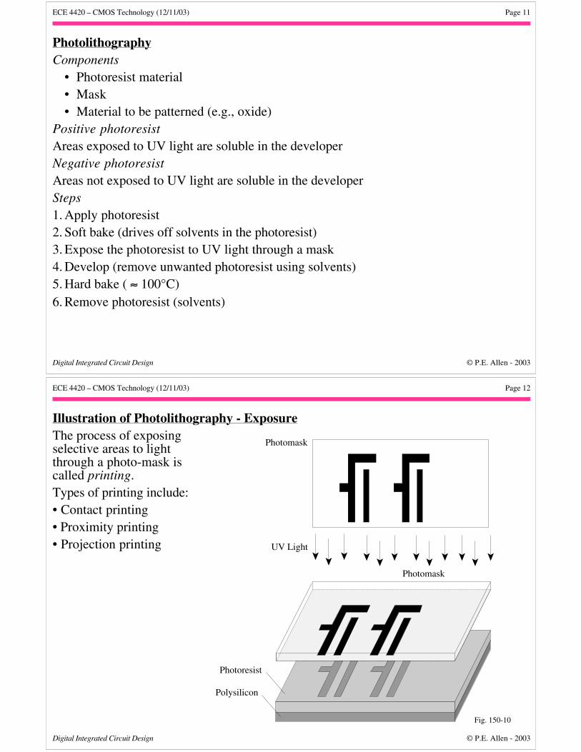
PhotolithographyComponents
• Photoresist material• Mask• Material to be patterned (e.g., oxide)
Positive photoresistAreas exposed to UV light are soluble in the developerNegative photoresistAreas not exposed to UV light are soluble in the developerSteps1. Apply photoresist2. Soft bake (drives off solvents in the photoresist)3. Expose the photoresist to UV light through a mask4. Develop (remove unwanted photoresist using solvents)5. Hard bake ( ≈ 100°C)6. Remove photoresist (solvents)
ECE 4420 – CMOS Technology (12/11/03) Page 12
Digital Integrated Circuit Design © P.E. Allen - 2003
Illustration of Photolithography - ExposureThe process of exposingselective areas to lightthrough a photo-mask iscalled printing.Types of printing include:• Contact printing• Proximity printing• Projection printing
Photoresist
Photomask
UV Light
Photomask
Polysilicon
Fig. 150-10
ECE 4420 – CMOS Technology (12/11/03) Page 13
Digital Integrated Circuit Design © P.E. Allen - 2003
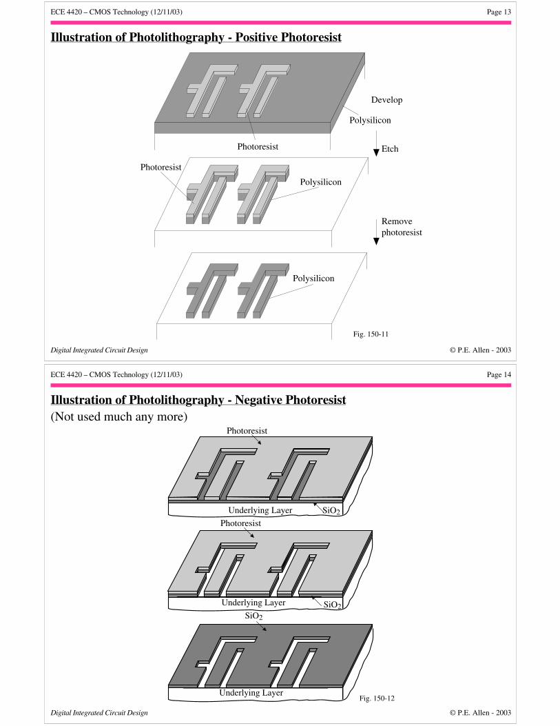
Illustration of Photolithography - Positive Photoresist
Photoresist
Photoresist
Polysilicon
Polysilicon
Polysilicon
Etch
Removephotoresist
Develop
Fig. 150-11
ECE 4420 – CMOS Technology (12/11/03) Page 14
Digital Integrated Circuit Design © P.E. Allen - 2003
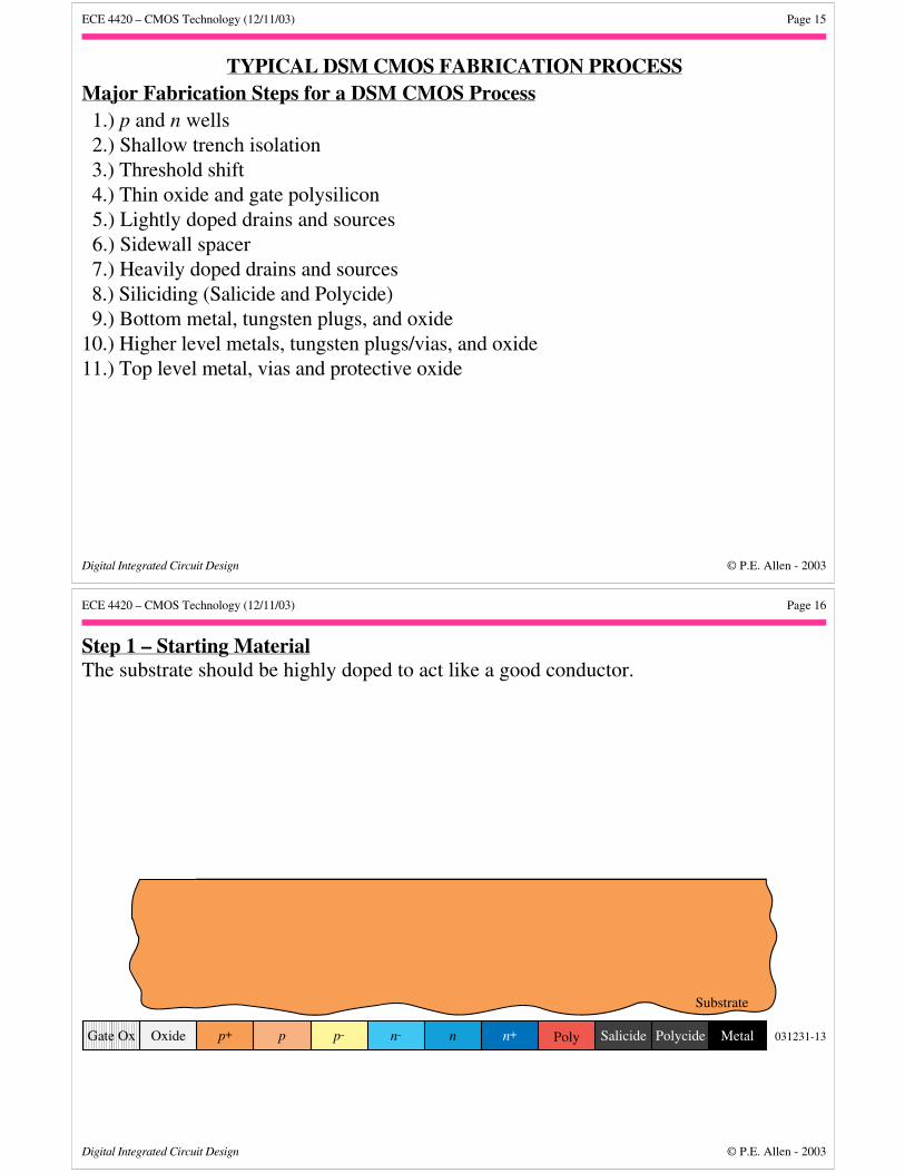
Illustration of Photolithography - Negative Photoresist(Not used much any more)
Underlying Layer
Underlying Layer
Underlying Layer
SiO2
Photoresist
SiO2
SiO2
Fig. 150-12
Photoresist
ECE 4420 – CMOS Technology (12/11/03) Page 15
Digital Integrated Circuit Design © P.E. Allen - 2003
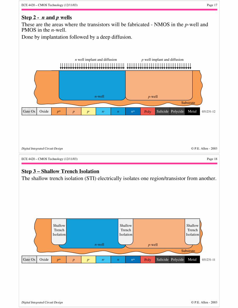
TYPICAL DSM CMOS FABRICATION PROCESSMajor Fabrication Steps for a DSM CMOS Process 1.) p and n wells 2.) Shallow trench isolation 3.) Threshold shift 4.) Thin oxide and gate polysilicon 5.) Lightly doped drains and sources 6.) Sidewall spacer 7.) Heavily doped drains and sources 8.) Siliciding (Salicide and Polycide) 9.) Bottom metal, tungsten plugs, and oxide10.) Higher level metals, tungsten plugs/vias, and oxide11.) Top level metal, vias and protective oxide
ECE 4420 – CMOS Technology (12/11/03) Page 16
Digital Integrated Circuit Design © P.E. Allen - 2003
Step 1 – Starting MaterialThe substrate should be highly doped to act like a good conductor.
p+ p p- MetalSaliciden- n n+Oxide Poly
Substrate
031231-13Polycide
yyGate Ox
ECE 4420 – CMOS Technology (12/11/03) Page 17
Digital Integrated Circuit Design © P.E. Allen - 2003
Step 2 - n and p wellsThese are the areas where the transistors will be fabricated - NMOS in the p-well andPMOS in the n-well.Done by implantation followed by a deep diffusion.
p+ p p- MetalSaliciden- n n+Oxide
n-well p-well
Poly
Substrate
031231-12Polycide
yyGate Ox
n well implant and diffusion p well implant and diffusion
ECE 4420 – CMOS Technology (12/11/03) Page 18
Digital Integrated Circuit Design © P.E. Allen - 2003
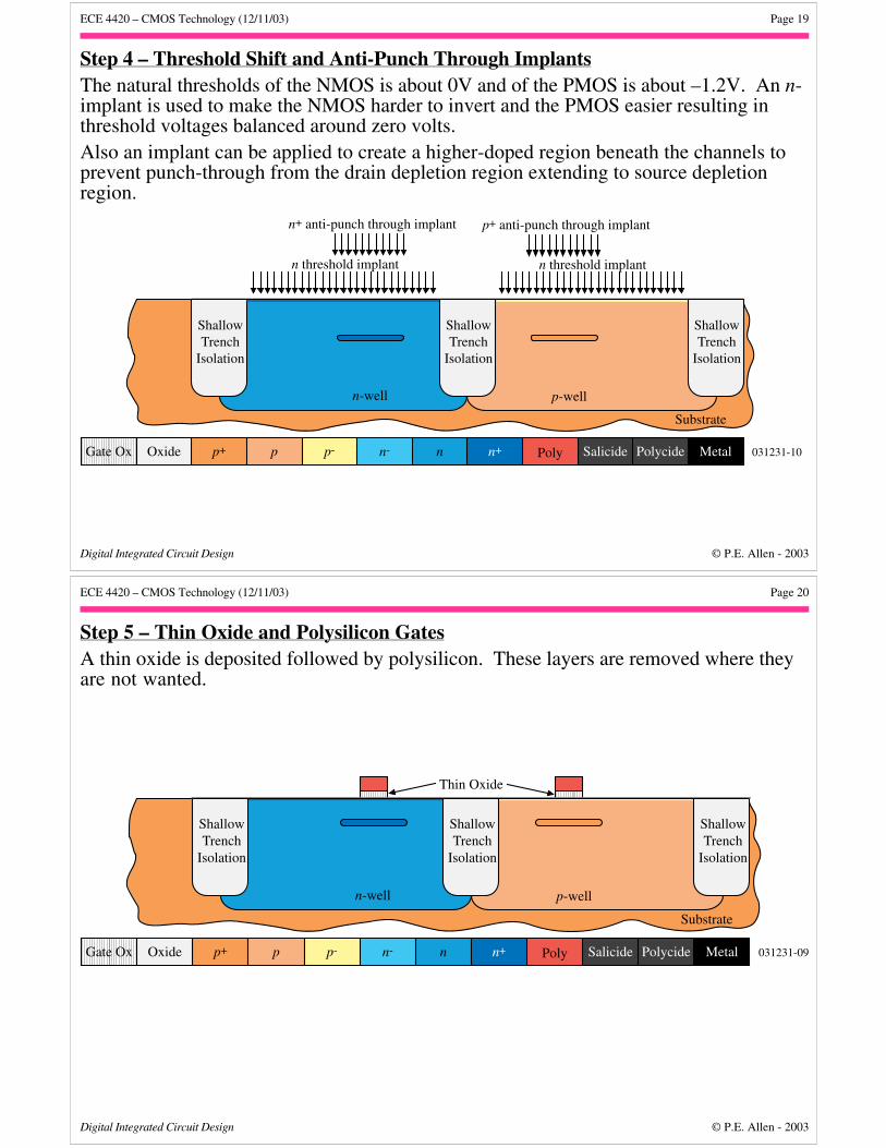
Step 3 – Shallow Trench IsolationThe shallow trench isolation (STI) electrically isolates one region/transistor from another.
p+ p p- MetalSaliciden- n n+Oxide
n-well p-well
Poly
ShallowTrench
Isolation
ShallowTrench
Isolation
ShallowTrench
Isolation
Substrate
031231-11Polycide
yyGate Ox
ECE 4420 – CMOS Technology (12/11/03) Page 19
Digital Integrated Circuit Design © P.E. Allen - 2003
Step 4 – Threshold Shift and Anti-Punch Through ImplantsThe natural thresholds of the NMOS is about 0V and of the PMOS is about –1.2V. An n-implant is used to make the NMOS harder to invert and the PMOS easier resulting inthreshold voltages balanced around zero volts.Also an implant can be applied to create a higher-doped region beneath the channels toprevent punch-through from the drain depletion region extending to source depletionregion.
p+ p p- MetalSaliciden- n n+Oxide
n-well p-well
Poly
Substrate
031231-10Polycide
yyGate Ox
n threshold implant n threshold implant
n+ anti-punch through implant p+ anti-punch through implant
ShallowTrench
Isolation
ShallowTrench
Isolation
ShallowTrench
Isolation
ECE 4420 – CMOS Technology (12/11/03) Page 20
Digital Integrated Circuit Design © P.E. Allen - 2003
Step 5 – Thin Oxide and Polysilicon GatesA thin oxide is deposited followed by polysilicon. These layers are removed where theyare not wanted.
p+ p p- MetalSaliciden- n n+Oxide
n-well p-well
Poly
Substrate
031231-09Polycide
yyGate Ox
Thin Oxide ShallowTrench
Isolation
ShallowTrench
Isolation
ShallowTrench
Isolation
ECE 4420 – CMOS Technology (12/11/03) Page 21
Digital Integrated Circuit Design © P.E. Allen - 2003
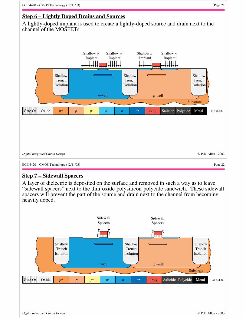
Step 6 – Lightly Doped Drains and SourcesA lightly-doped implant is used to create a lightly-doped source and drain next to thechannel of the MOSFETs.
p+ p p- MetalSaliciden- n n+Oxide
n-well p-well
Poly
Substrate
031231-08Polycide
yyGate Ox
Shallow n-
ImplantShallow n-
ImplantShallow p-
ImplantShallow p-
Implant ShallowTrench
Isolation
ShallowTrench
Isolation
ShallowTrench
Isolation
ECE 4420 – CMOS Technology (12/11/03) Page 22
Digital Integrated Circuit Design © P.E. Allen - 2003
Step 7 – Sidewall SpacersA layer of dielectric is deposited on the surface and removed in such a way as to leave“sidewall spacers” next to the thin-oxide-polysilicon-polycide sandwich. These sidewallspacers will prevent the part of the source and drain next to the channel from becomingheavily doped.
p+ p p- MetalSaliciden- n n+Oxide
n-well p-well
Poly
SidewallSpacers
Substrate
031231-07Polycide
yyGate Ox
SidewallSpacers
ShallowTrench
Isolation
ShallowTrench
Isolation
ShallowTrench
Isolation
ECE 4420 – CMOS Technology (12/11/03) Page 23
Digital Integrated Circuit Design © P.E. Allen - 2003
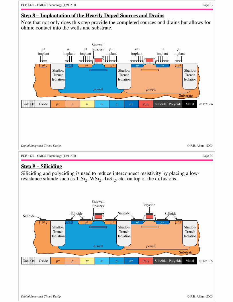
Step 8 – Implantation of the Heavily Doped Sources and DrainsNote that not only does this step provide the completed sources and drains but allows forohmic contact into the wells and substrate.
p+ p p- MetalSaliciden- n n+Oxide
n-well p-well
Poly
Substrate
031231-06
p+
Polycide
yyGate Ox
p+
implantn+
implantn+
implantp+
implantp+
implantp+
implantn+
implant SidewallSpacers
n+ n+p+ p+
ShallowTrench
Isolation
ShallowTrench
Isolation
ShallowTrench
Isolation
p+n+
ECE 4420 – CMOS Technology (12/11/03) Page 24
Digital Integrated Circuit Design © P.E. Allen - 2003
Step 9 – SilicidingSiliciding and polyciding is used to reduce interconnect resistivity by placing a low-resistance silicide such as TiSi2, WSi2, TaSi2, etc. on top of the diffusions.
p+ p p- MetalSaliciden- n n+Oxide
n-well p-well
Poly
ShallowTrench
Isolation
Substrate
031231-05
p+
Polycide
yyGate Ox
SidewallSpacers
Salicide Salicide
Polycide
SalicideSalicide
n+ n+p+ p+
ShallowTrench
Isolation
ShallowTrench
Isolation
p+n+
ECE 4420 – CMOS Technology (12/11/03) Page 25
Digital Integrated Circuit Design © P.E. Allen - 2003
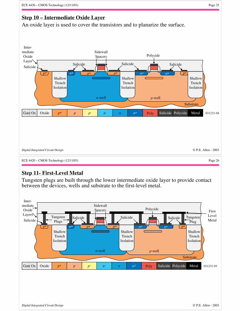
Step 10 – Intermediate Oxide LayerAn oxide layer is used to cover the transistors and to planarize the surface.
p+ p p- MetalSaliciden- n n+Oxide
n-well p-well
Poly
SidewallSpacers
Salicide Salicide
Polycide
Salicide
Substrate
Inter-mediateOxideLayer
031231-04
p+
Salicide
Polycide
yyGate Ox
n+ n+p+ p+
ShallowTrench
Isolation
ShallowTrench
Isolation
ShallowTrench
Isolation
p+n+
ECE 4420 – CMOS Technology (12/11/03) Page 26
Digital Integrated Circuit Design © P.E. Allen - 2003
Step 11- First-Level MetalTungsten plugs are built through the lower intermediate oxide layer to provide contactbetween the devices, wells and substrate to the first-level metal.
p+ p p- MetalSaliciden- n n+Oxide
n-well p-well
Poly
Substrate
031231-03
p+
Polycide
yyGate Ox
Salicide Salicide SalicideSalicide
FirstLevelMetal
Inter-mediateOxideLayers
TungstenPlugs
TungstenPlug
SidewallSpacers Polycide
n+ n+p+ p+
ShallowTrench
Isolation
ShallowTrench
Isolation
ShallowTrench
Isolation
p+n+
ECE 4420 – CMOS Technology (12/11/03) Page 27
Digital Integrated Circuit Design © P.E. Allen - 2003
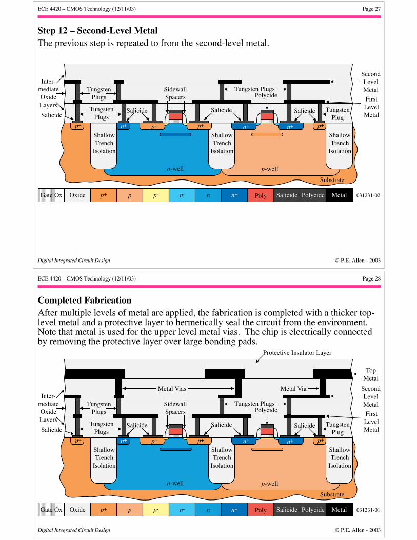
Step 12 – Second-Level MetalThe previous step is repeated to from the second-level metal.
p+ p p- MetalSaliciden- n n+Oxide
n-well p-well
Poly
ShallowTrench
Isolation
Substrate
031231-02
p+
Polycide
yyGate Ox
Salicide Salicide SalicideSalicide
FirstLevelMetal
TungstenPlugs
TungstenPlug
SidewallSpacers Polycide
SecondLevel MetalTungsten Plugs
Inter-mediateOxideLayers
TungstenPlugs
n+ n+p+ p+
ShallowTrench
Isolation
ShallowTrench
Isolation
p+n+
ECE 4420 – CMOS Technology (12/11/03) Page 28
Digital Integrated Circuit Design © P.E. Allen - 2003
Completed FabricationAfter multiple levels of metal are applied, the fabrication is completed with a thicker top-level metal and a protective layer to hermetically seal the circuit from the environment.Note that metal is used for the upper level metal vias. The chip is electrically connectedby removing the protective layer over large bonding pads.
p+ p p- MetalSaliciden- n n+Oxide
n-well p-well
Poly
ShallowTrench
Isolation
SidewallSpacers Polycide
Top Metal
SecondLevel Metal
FirstLevelMetal
Tungsten Plugs
Protective Insulator Layer
Substrate
Inter-mediateOxideLayers
031231-01
Metal Vias Metal Via
p+
Polycide
TungstenPlugs
yyGate Ox
Salicide Salicide SalicideSalicide
TungstenPlugs
TungstenPlug
n+ n+p+ p+
ShallowTrench
Isolation
ShallowTrench
Isolation
p+n+
ECE 4420 – CMOS Technology (12/11/03) Page 29
Digital Integrated Circuit Design © P.E. Allen - 2003
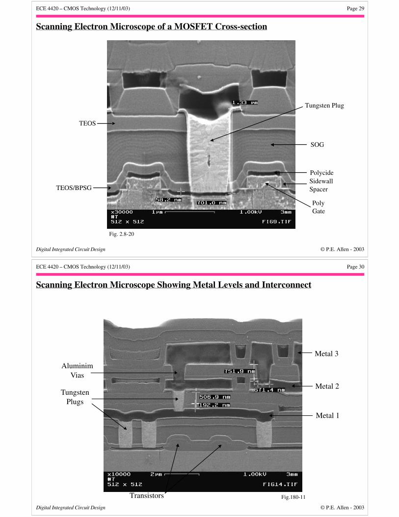
Scanning Electron Microscope of a MOSFET Cross-section
Fig. 2.8-20
TEOS
TEOS/BPSG
Tungsten Plug
SOG
Polycide
PolyGate
SidewallSpacer
ECE 4420 – CMOS Technology (12/11/03) Page 30
Digital Integrated Circuit Design © P.E. Allen - 2003
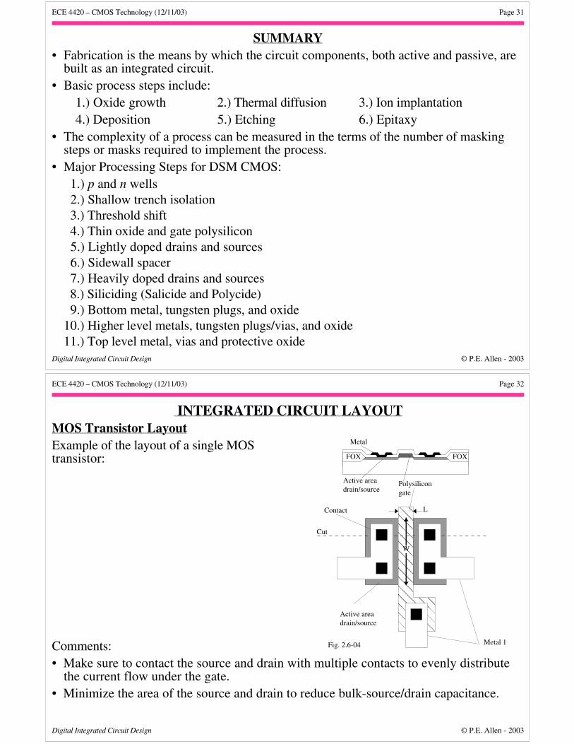
Scanning Electron Microscope Showing Metal Levels and Interconnect
Fig.180-11
Metal 1
Metal 2
Metal 3
TungstenPlugs
AluminimVias
Transistors
ECE 4420 – CMOS Technology (12/11/03) Page 31
Digital Integrated Circuit Design © P.E. Allen - 2003
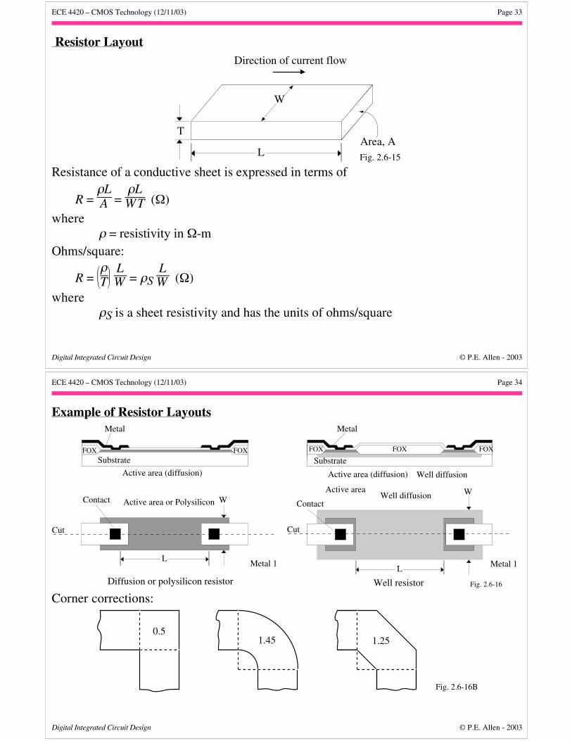
SUMMARY• Fabrication is the means by which the circuit components, both active and passive, are
built as an integrated circuit.• Basic process steps include:
1.) Oxide growth 2.) Thermal diffusion 3.) Ion implantation4.) Deposition 5.) Etching 6.) Epitaxy
• The complexity of a process can be measured in the terms of the number of maskingsteps or masks required to implement the process.
• Major Processing Steps for DSM CMOS: 1.) p and n wells 2.) Shallow trench isolation 3.) Threshold shift 4.) Thin oxide and gate polysilicon 5.) Lightly doped drains and sources 6.) Sidewall spacer 7.) Heavily doped drains and sources 8.) Siliciding (Salicide and Polycide) 9.) Bottom metal, tungsten plugs, and oxide10.) Higher level metals, tungsten plugs/vias, and oxide11.) Top level metal, vias and protective oxide
ECE 4420 – CMOS Technology (12/11/03) Page 32
Digital Integrated Circuit Design © P.E. Allen - 2003
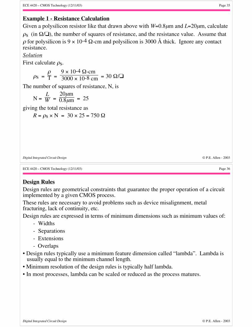
INTEGRATED CIRCUIT LAYOUTMOS Transistor LayoutExample of the layout of a single MOStransistor:
Comments:• Make sure to contact the source and drain with multiple contacts to evenly distribute
the current flow under the gate.• Minimize the area of the source and drain to reduce bulk-source/drain capacitance.
Contact
Polysilicongate
Active areadrain/source
Metal 1
W
L
Cut
FOX FOX
Metal
Active areadrain/source
Fig. 2.6-04
ECE 4420 – CMOS Technology (12/11/03) Page 33
Digital Integrated Circuit Design © P.E. Allen - 2003
Resistor Layout
L
W
T
Direction of current flow
Area, AFig. 2.6-15
Resistance of a conductive sheet is expressed in terms of
R = ρLA =
ρLWT (Ω)
whereρ = resistivity in Ω-m
Ohms/square:
R =
ρ
T LW = ρS
LW (Ω)
whereρS is a sheet resistivity and has the units of ohms/square
ECE 4420 – CMOS Technology (12/11/03) Page 34
Digital Integrated Circuit Design © P.E. Allen - 2003
Example of Resistor Layouts
Metal 1
Active area or PolysiliconContact
Diffusion or polysilicon resistor
L
W
Metal 1
Well diffusionContact
Well resistor
L
WActive area
FOX FOXFOX
Metal
Active area (diffusion)
FOX FOX
Metal
Active area (diffusion) Well diffusion
CutCut
Substrate Substrate
Fig. 2.6-16
Corner corrections:
0.51.45 1.25
Fig. 2.6-16B
ECE 4420 – CMOS Technology (12/11/03) Page 35
Digital Integrated Circuit Design © P.E. Allen - 2003
Example 1 - Resistance CalculationGiven a polysilicon resistor like that drawn above with W=0.8µm and L=20µm, calculate
ρs (in Ω/), the number of squares of resistance, and the resistance value. Assume thatρ for polysilicon is 9 × 10⁻⁴ Ω-cm and polysilicon is 3000 Å thick. Ignore any contactresistance.SolutionFirst calculate ρs.
ρs = ρT =
9 × 10⁻⁴ Ω-cm 3000 × 10-8 cm = 30 Ω/
The number of squares of resistance, N, is
N = LW =
20µm0.8µm = 25
giving the total resistance asR = ρs × Ν = 30 × 25 = 750 Ω
ECE 4420 – CMOS Technology (12/11/03) Page 36
Digital Integrated Circuit Design © P.E. Allen - 2003
Design RulesDesign rules are geometrical constraints that guarantee the proper operation of a circuitimplemented by a given CMOS process.These rules are necessary to avoid problems such as device misalignment, metalfracturing, lack of continuity, etc.Design rules are expressed in terms of minimum dimensions such as minimum values of:
- Widths- Separations- Extensions- Overlaps
• Design rules typically use a minimum feature dimension called “lambda”. Lambda isusually equal to the minimum channel length.
• Minimum resolution of the design rules is typically half lambda.• In most processes, lambda can be scaled or reduced as the process matures.
ECE 4420 – CMOS Technology (12/11/03) Page 37
Digital Integrated Circuit Design © P.E. Allen - 2003
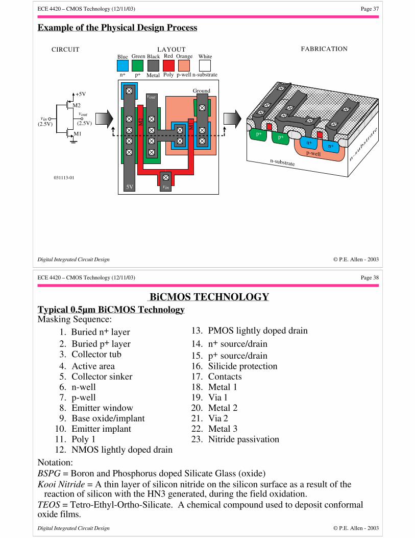
Example of the Physical Design Process
n+ p+ Metal Poly p-well n-substrate
Blue RedBlack OrangeGreen White
5V vin
voutGround
M2
M1
+5V
voutvin
M2
M1
031113-01
(2.5V) (2.5V)
p+
yyp+
n+n+
p-welln-substrate
yy
n-s
ubstra
te
CIRCUIT LAYOUT FABRICATION
ECE 4420 – CMOS Technology (12/11/03) Page 38
Digital Integrated Circuit Design © P.E. Allen - 2003
BiCMOS TECHNOLOGYTypical 0.5µm BiCMOS TechnologyMasking Sequence:
1. Buried n+ layer 13. PMOS lightly doped drain
2. Buried p+ layer 14. n+ source/drain 3. Collector tub 15. p+ source/drain 4. Active area 16. Silicide protection 5. Collector sinker 17. Contacts 6. n-well 18. Metal 1 7. p-well 19. Via 1 8. Emitter window 20. Metal 2 9. Base oxide/implant 21. Via 210. Emitter implant 22. Metal 311. Poly 1 23. Nitride passivation12. NMOS lightly doped drain
Notation:BSPG = Boron and Phosphorus doped Silicate Glass (oxide)Kooi Nitride = A thin layer of silicon nitride on the silicon surface as a result of the
reaction of silicon with the HN3 generated, during the field oxidation.TEOS = Tetro-Ethyl-Ortho-Silicate. A chemical compound used to deposit conformaloxide films.
ECE 4420 – CMOS Technology (12/11/03) Page 39
Digital Integrated Circuit Design © P.E. Allen - 2003
n+ and p+ Buried Layers
Starting Substrate:
p-substrate 1µm
5µmBiCMOS-01
n+ and p+ Buried Layers:
p-substrate
n+ buried layer p+ buriedlayer
n+ buried layer p+ buried layer
1µm
5µm
NMOS TransistorPMOS TransistorNPN Transistor
BiCMOS-02
ECE 4420 – CMOS Technology (12/11/03) Page 40
Digital Integrated Circuit Design © P.E. Allen - 2003
Epitaxial Growth
p-substrate
n+ buried layer p+ buriedlayer
n+ buried layerp+ buried layer
p-typeEpitaxialSilicon
p-well n-well p-well
1µm
5µm
NMOS TransistorPMOS TransistorNPN Transistor
n-well
BiCMOS-03
Comment:• As the epi layer grows vertically, it assumes the doping level of the substrate beneath it.• In addition, the high temperature of the epitaxial process causes the buried layers to
diffuse upward and downward.
ECE 4420 – CMOS Technology (12/11/03) Page 41
Digital Integrated Circuit Design © P.E. Allen - 2003
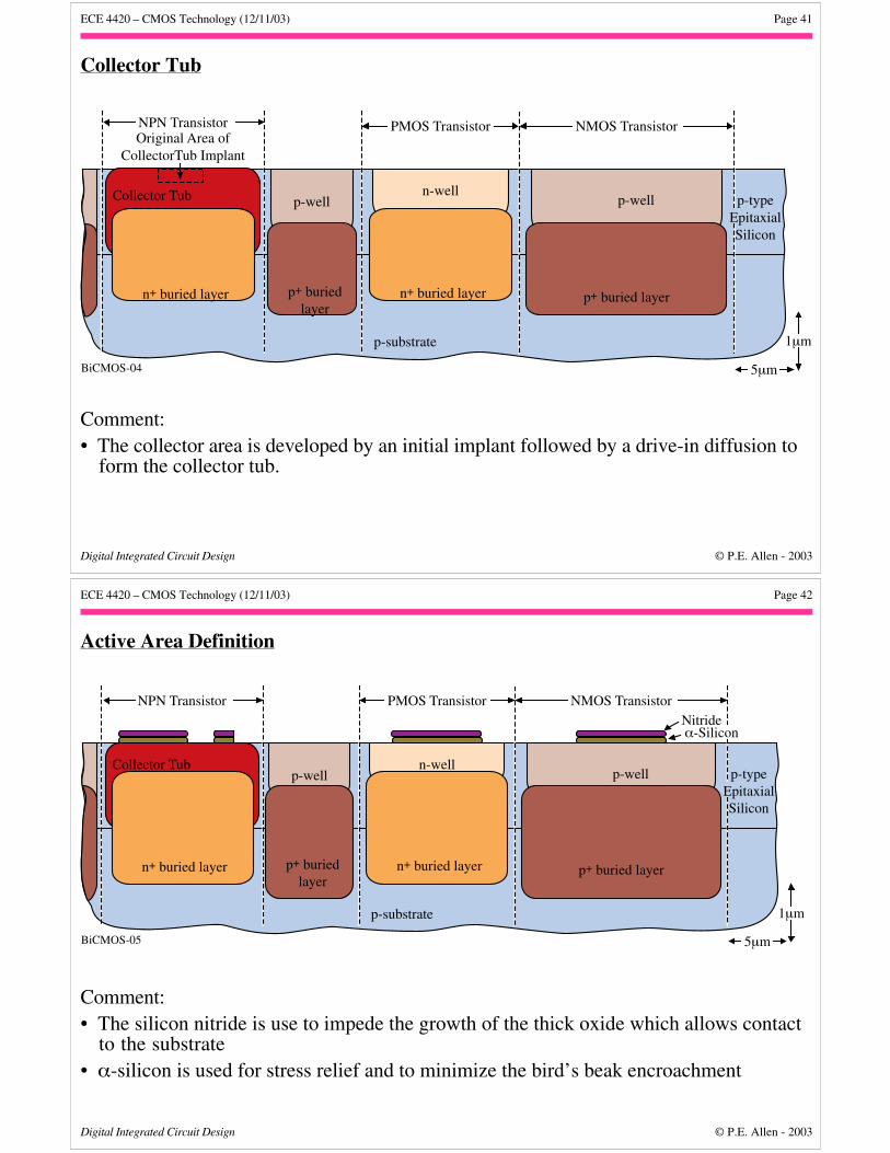
Collector Tub
p-substrate
n+ buried layer p+ buriedlayer
n+ buried layer p+ buried layer
p-typeEpitaxialSilicon
p-welln-well
p-well
1µm
5µm
Collector Tub
NMOS TransistorPMOS TransistorNPN Transistor
BiCMOS-04
Original Area of CollectorTub Implant
Comment:• The collector area is developed by an initial implant followed by a drive-in diffusion to
form the collector tub.
ECE 4420 – CMOS Technology (12/11/03) Page 42
Digital Integrated Circuit Design © P.E. Allen - 2003
Active Area Definition
p-substrate
n+ buried layer p+ buriedlayer
n+ buried layer p+ buried layer
p-typeEpitaxialSilicon
p-welln-well
p-well
1µm
5µm
Collector Tub
NMOS TransistorPMOS TransistorNPN Transistor
BiCMOS-05
Nitrideα-Silicon
Comment:• The silicon nitride is use to impede the growth of the thick oxide which allows contact
to the substrate• α-silicon is used for stress relief and to minimize the bird’s beak encroachment
ECE 4420 – CMOS Technology (12/11/03) Page 43
Digital Integrated Circuit Design © P.E. Allen - 2003
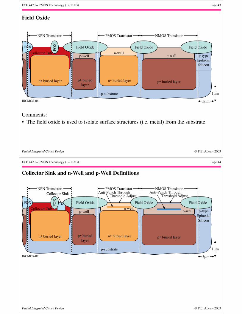
Field Oxide
p-substrate
n+ buried layer p+ buriedlayer
n+ buried layer p+ buried layer
p-typeEpitaxialSilicon
FOX
p-welln-well
p-well
1µm
5µm
Collector Tub
Field Oxide Field Oxide
NMOS TransistorPMOS TransistorNPN Transistor
BiCMOS-06
FOX Field Oxide
Comments:• The field oxide is used to isolate surface structures (i.e. metal) from the substrate
ECE 4420 – CMOS Technology (12/11/03) Page 44
Digital Integrated Circuit Design © P.E. Allen - 2003
Collector Sink and n-Well and p-Well Definitions
p-substrate
n+ buried layer p+ buriedlayer
n+ buried layer p+ buried layer
p-typeEpitaxialSilicon
p-well p-well
1µm
5µm
Collector Tub
Field Oxide
NMOS TransistorPMOS TransistorNPN Transistor
BiCMOS-07
FOX
Field Oxide
Collector Sink Anti-Punch ThroughThreshold Adjust
Anti-Punch ThroughThreshold Adjust
n-well
FOX Field Oxide
ECE 4420 – CMOS Technology (12/11/03) Page 45
Digital Integrated Circuit Design © P.E. Allen - 2003
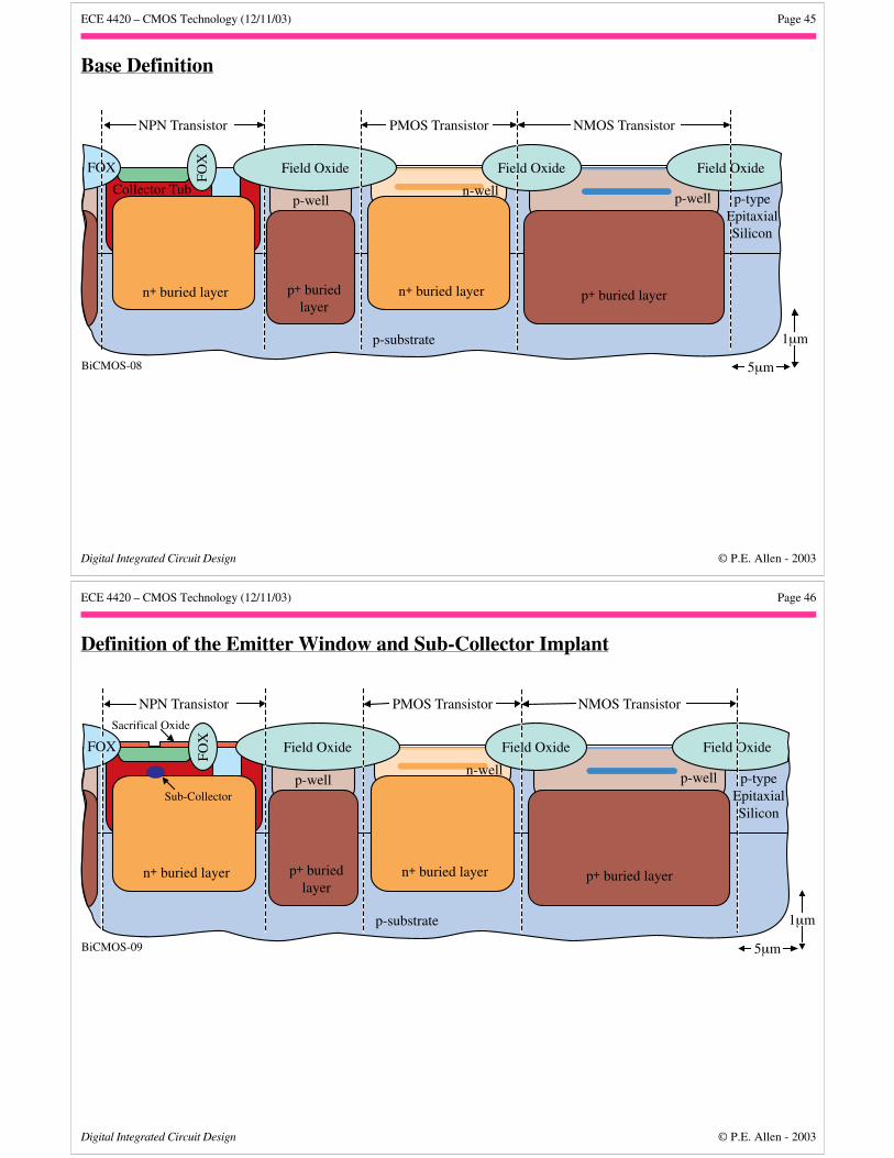
Base Definition
p-substrate
n+ buried layer p+ buriedlayer
n+ buried layer p+ buried layer
p-typeEpitaxialSilicon
FOX
p-well p-well
1µm
5µm
Collector Tub
NMOS TransistorPMOS TransistorNPN Transistor
BiCMOS-08
Field Oxide Field Oxide
n-well
FOX Field Oxide
ECE 4420 – CMOS Technology (12/11/03) Page 46
Digital Integrated Circuit Design © P.E. Allen - 2003
Definition of the Emitter Window and Sub-Collector Implant
p-substrate
n+ buried layer p+ buriedlayer
n+ buried layer p+ buried layer
p-typeEpitaxialSilicon
p-well p-well
1µm
5µm
NMOS TransistorPMOS TransistorNPN Transistor
BiCMOS-09
Field Oxide
n-well
Sub-Collector
FOX
Field Oxide
Sacrifical Oxide
FOX Field Oxide
ECE 4420 – CMOS Technology (12/11/03) Page 47
Digital Integrated Circuit Design © P.E. Allen - 2003
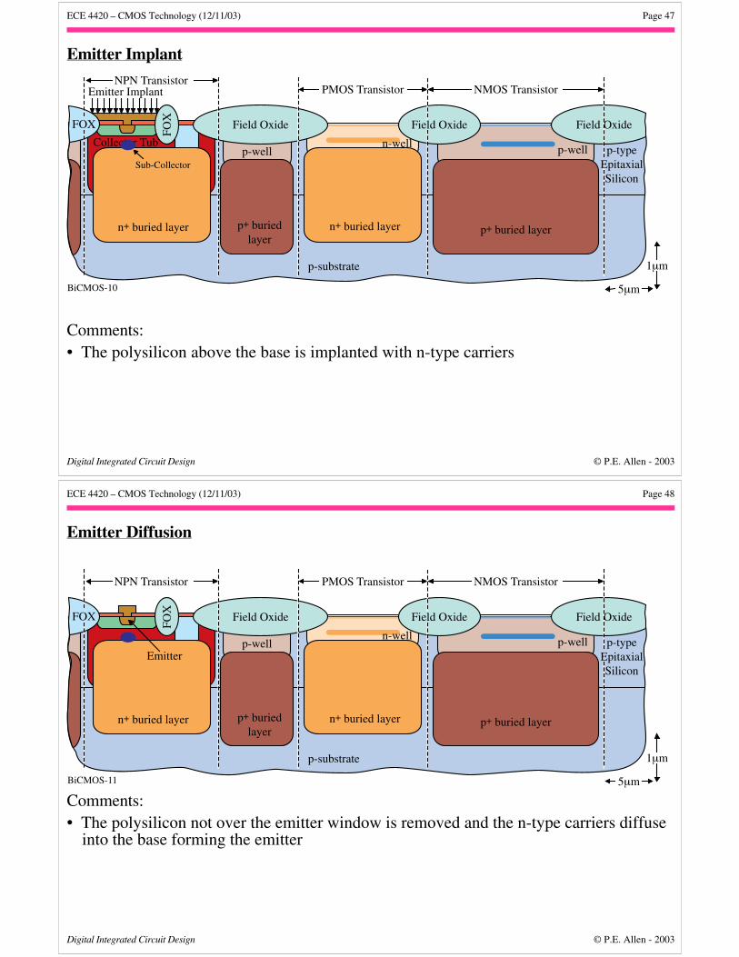
Emitter Implant
p-substrate
n+ buried layer p+ buriedlayer
n+ buried layer p+ buried layer
p-typeEpitaxialSilicon
p-well p-well
1µm
5µm
Collector Tub
NMOS TransistorPMOS TransistorNPN Transistor
BiCMOS-10
Field Oxide
n-well
Sub-CollectorFO
X
Field Oxide
Emitter Implant
FOX Field Oxide
Comments:• The polysilicon above the base is implanted with n-type carriers
ECE 4420 – CMOS Technology (12/11/03) Page 48
Digital Integrated Circuit Design © P.E. Allen - 2003
Emitter Diffusion
p-substrate
n+ buried layer p+ buriedlayer
n+ buried layer p+ buried layer
p-typeEpitaxialSilicon
p-well p-well
1µm
5µm
NMOS TransistorPMOS TransistorNPN Transistor
BiCMOS-11
Field Oxide
n-well
FOX
Field Oxide
Emitter
FOX Field Oxide
Comments:• The polysilicon not over the emitter window is removed and the n-type carriers diffuse
into the base forming the emitter
ECE 4420 – CMOS Technology (12/11/03) Page 49
Digital Integrated Circuit Design © P.E. Allen - 2003
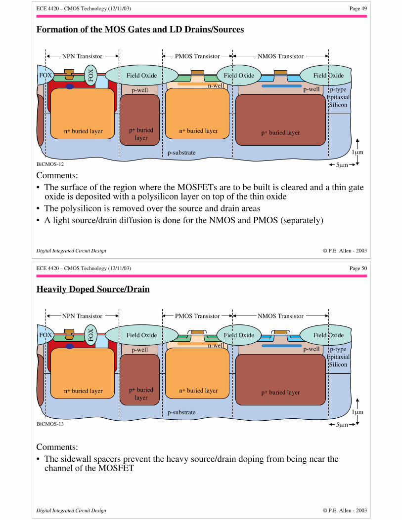
Formation of the MOS Gates and LD Drains/Sources
p-substrate
n+ buried layer p+ buriedlayer
n+ buried layer p+ buried layer
p-typeEpitaxialSilicon
p-well p-well
1µm
5µm
NMOS TransistorPMOS TransistorNPN Transistor
BiCMOS-12
Field Oxide
n-wellFO
X
Field OxideFOX Field Oxide
Comments:• The surface of the region where the MOSFETs are to be built is cleared and a thin gate
oxide is deposited with a polysilicon layer on top of the thin oxide• The polysilicon is removed over the source and drain areas• A light source/drain diffusion is done for the NMOS and PMOS (separately)
ECE 4420 – CMOS Technology (12/11/03) Page 50
Digital Integrated Circuit Design © P.E. Allen - 2003
Heavily Doped Source/Drain
p-substrate
n+ buried layer p+ buriedlayer
n+ buried layer p+ buried layer
p-typeEpitaxialSilicon
p-well p-well
1µm
5µm
NMOS TransistorPMOS TransistorNPN Transistor
BiCMOS-13
Field Oxide
n-well
FOX
Field OxideFOX Field Oxide
Comments:• The sidewall spacers prevent the heavy source/drain doping from being near the
channel of the MOSFET
ECE 4420 – CMOS Technology (12/11/03) Page 51
Digital Integrated Circuit Design © P.E. Allen - 2003
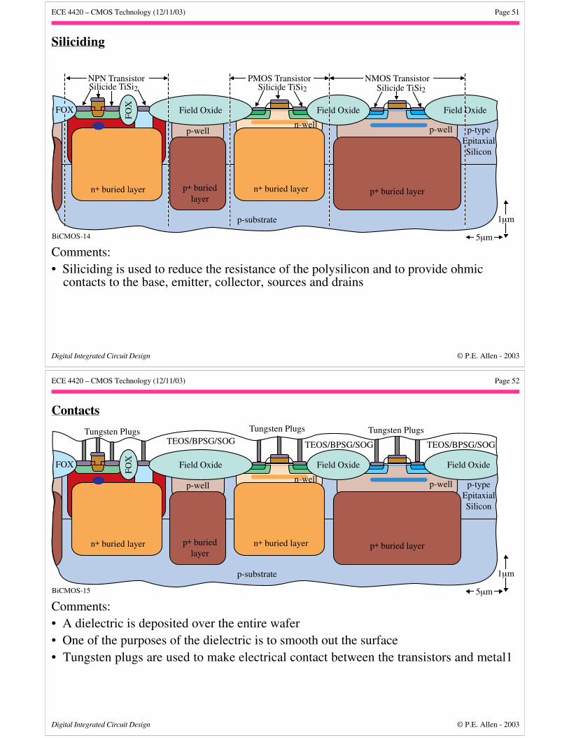
Siliciding
p-substrate
n+ buried layer p+ buriedlayer
n+ buried layer p+ buried layer
p-typeEpitaxialSilicon
p-well p-well
1µm
5µm
NMOS TransistorPMOS TransistorNPN Transistor
BiCMOS-14
Field Oxide
n-wellFO
X
Field Oxide
Silicide TiSi2 Silicide TiSi2 Silicide TiSi2
FOX Field Oxide
Comments:• Siliciding is used to reduce the resistance of the polysilicon and to provide ohmic
contacts to the base, emitter, collector, sources and drains
ECE 4420 – CMOS Technology (12/11/03) Page 52
Digital Integrated Circuit Design © P.E. Allen - 2003
Contacts
p-substrate
n+ buried layer p+ buriedlayer
n+ buried layer p+ buried layer
p-typeEpitaxialSilicon
p-well p-well
1µm
5µmBiCMOS-15
Field Oxide Field Oxide
n-well
FOX
Field Oxide Field Oxide
Tungsten Plugs Tungsten PlugsTungsten PlugsTEOS/BPSG/SOG TEOS/BPSG/SOG TEOS/BPSG/SOG
FOX
Comments:• A dielectric is deposited over the entire wafer• One of the purposes of the dielectric is to smooth out the surface• Tungsten plugs are used to make electrical contact between the transistors and metal1
ECE 4420 – CMOS Technology (12/11/03) Page 53
Digital Integrated Circuit Design © P.E. Allen - 2003
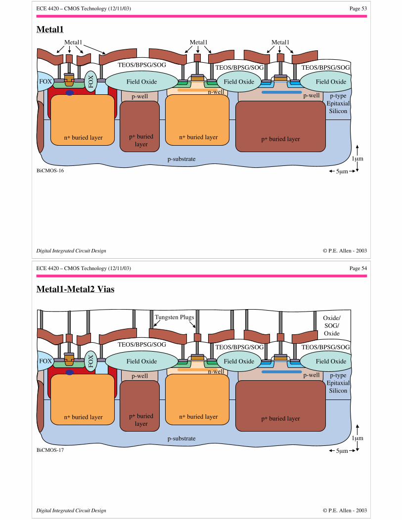
Metal1
p-substrate
n+ buried layer p+ buriedlayer
n+ buried layer p+ buried layer
p-typeEpitaxialSilicon
p-well p-well
1µm
5µmBiCMOS-16
Field Oxide Field Oxide
n-wellFO
XField Oxide Field Oxide
TEOS/BPSG/SOG TEOS/BPSG/SOG TEOS/BPSG/SOG
Metal1 Metal1Metal1
FOX
ECE 4420 – CMOS Technology (12/11/03) Page 54
Digital Integrated Circuit Design © P.E. Allen - 2003
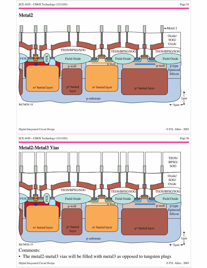
Metal1-Metal2 Vias
p-substrate
n+ buried layer p+ buriedlayer
n+ buried layer p+ buried layer
p-typeEpitaxialSilicon
p-well p-well
1µm
5µmBiCMOS-17
Field Oxide Field Oxide
n-well
FOX
Field Oxide Field Oxide
TEOS/BPSG/SOG TEOS/BPSG/SOG TEOS/BPSG/SOG
Tungsten Plugs Oxide/SOG/Oxide
FOX
ECE 4420 – CMOS Technology (12/11/03) Page 55
Digital Integrated Circuit Design © P.E. Allen - 2003
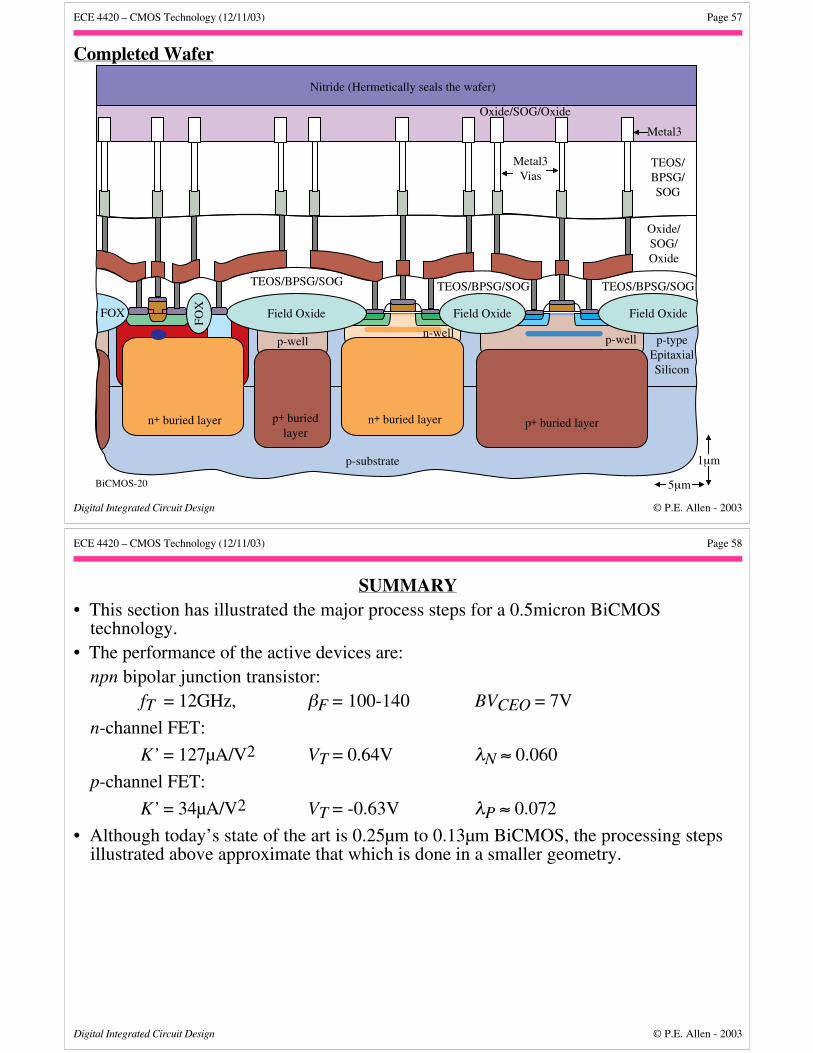
Metal2
p-substrate
n+ buried layer p+ buriedlayer
n+ buried layer p+ buried layer
p-typeEpitaxialSilicon
p-well p-well
1µm
5µmBiCMOS-18
Field Oxide Field Oxide
n-well
FOX
Field Oxide Field Oxide
TEOS/BPSG/SOG TEOS/BPSG/SOG TEOS/BPSG/SOG
Metal 2
FOX
Oxide/SOG/Oxide
ECE 4420 – CMOS Technology (12/11/03) Page 56
Digital Integrated Circuit Design © P.E. Allen - 2003
Metal2-Metal3 Vias
p-substrate
n+ buried layer p+ buriedlayer
n+ buried layer p+ buried layer
p-typeEpitaxialSilicon
p-well p-well
1µm
5µmBiCMOS-19
Field Oxide Field Oxide
n-well
FOX
Field Oxide Field Oxide
TEOS/BPSG/SOG TEOS/BPSG/SOG TEOS/BPSG/SOG
FOX
TEOS/BPSG/SOG
Oxide/SOG/Oxide
Comments:• The metal2-metal3 vias will be filled with metal3 as opposed to tungsten plugs
ECE 4420 – CMOS Technology (12/11/03) Page 57
Digital Integrated Circuit Design © P.E. Allen - 2003
Completed Wafer
p-substrate
n+ buried layer p+ buriedlayer
n+ buried layer p+ buried layer
p-typeEpitaxialSilicon
p-well p-well
1µm
5µmBiCMOS-20
Field Oxide Field Oxide
n-well
FOX
Field Oxide Field Oxide
TEOS/BPSG/SOG TEOS/BPSG/SOG TEOS/BPSG/SOG
Nitride (Hermetically seals the wafer)
FOX
TEOS/BPSG/SOG
Metal3
Oxide/SOG/Oxide
Oxide/SOG/Oxide
Metal3Vias
ECE 4420 – CMOS Technology (12/11/03) Page 58
Digital Integrated Circuit Design © P.E. Allen - 2003
SUMMARY• This section has illustrated the major process steps for a 0.5micron BiCMOS
technology.• The performance of the active devices are:
npn bipolar junction transistor:fT = 12GHz, βF = 100-140 BVCEO = 7V
n-channel FET:
K’ = 127µA/V2 VT = 0.64V λN ≈ 0.060
p-channel FET:
K’ = 34µA/V2 VT = -0.63V λP ≈ 0.072
• Although today’s state of the art is 0.25µm to 0.13µm BiCMOS, the processing stepsillustrated above approximate that which is done in a smaller geometry.