Embed Size (px)
Citation preview
1
CMOS VLSI Design M.Tech. First semester VTU
Introduction
The present chapter first develops the fundamental physical characteristics of the MOS transistor, in which the
electrical currents and voltages are the most important quantities. The link between physical design and logic
networks can be established. Figure 2.1 depicts various symbols used for the MOS transistors. The symbol shown
in Figure 2.1(a) is used to indicate only switch logic, while that in Figure 2.1(b) shows the substrate connection.
Figure 2.1 Various symbols for MOS transistors This chapter first discusses about the basic electrical and physical properties of the Metal Oxide Semiconductor (MOS) transistors. The structure and operation of the nMOS and pMOS transistors are addressed, following which the concepts of threshold voltage and body effect are explained. The current-voltage equation of a MOS device for different regions of operation is next established. It is based on considering the effects of external bias conditions on charge distribution in MOS system and on conductance of free carriers on one hand, and the fact that the current flow depends only on the majority carrier flow between the two device terminals. Various second-order effects observed in MOSFETs are next dealt with. Subsequently, the complementary MOS (CMOS) inverter is taken up. Its DC characteristics, noise margin and the small-signal characteristics are discussed. Various load configurations of MOS inverters including passive resistance as well as transistors are presented. The differential inverter involving double-ended inputs and outputs are discussed. The complementary switch or the transmission gate, the tristate inverter and the bipolar devices are briefly dealt with.
2.1.1 nMOS and pMOS Enhancement Transistors
www.bookspar.com | VTU NOTES | QUESTION PAPERS | NEWS | RESULTS | FORUMS
www.bookspar.com | VTU NOTES | QUESTION PAPERS | NEWS | RESULTS | FORUMS
2
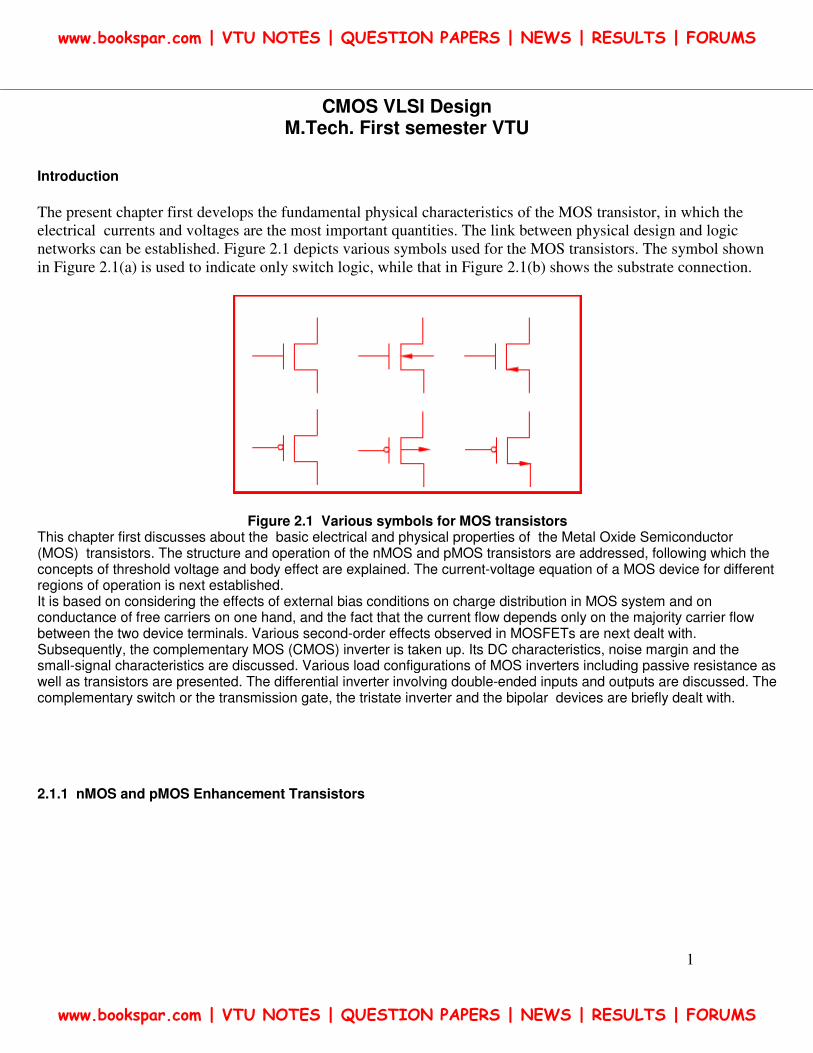
Figure 2.2 depicts a simplified view of the basic structure of an n-channel enhancement mode transistor, which is
formed on a p-type substrate of moderate doping level. As shown in the figure, the source and the drain regions
made of two isolated islands of n+-type diffusion. These two diffusion regions are connected via metal to the
external conductors. The depletion regions are mainly formed in the more lightly doped p-region. Thus, the source
and the drain are separated from each other by two diodes, as shown in Figure 2.2. A useful device can, however,
be made only be maintaining a current between the source and the drain. The region between the two diffused
islands under the oxide layer is called the channel region. The channel provides a path for the majority carriers
(electrons for example, in the n-channel device) to flow between the source and the drain.
The channel is covered by a thin insulating layer of silicon dioxide (SiO2). The gate electrode, made of
polycrystalline silicon (polysilicon or poly in short) stands over this oxide. As the oxide layer is an insulator, the
DC current from the gate to the channel is zero. The source and the drain regions are indistinguishable due to the
physical symmetry of the structure. The current carriers enter the device through the source terminal while they
leave the device by the drain.
The switching behaviour of a MOS device is characterized by an important parameter called the threshold voltage (Vth), which is defined as the minimum voltage, that must be established between the gate and the source (or between the gate and the substrate, if the source and the substrate are shorted together), to enable the device to conduct (or "turn on"). In the enhancement mode device, the channel is not established and the device is in a non-conducting (also called
cutoff or sub-threshold) state, for . If the gate is connected to a suitable positive voltage with respect to the source, then the electric field established between the gate and the source will induce a charge inversion region, whereby a conducting path is formed between the source and the drain. In the enhancement mode device, the formation of the channel is enhanced in the presence of the gate voltage.
Figure 2.2: Structure of an nMOS enhancement mode transistor. Note that VGS > Vth , and VDS =0.
By implanting suitable impurities in the region between the source and the drain before depositing the insulating oxide and the gate, a channel can also be established. Thus the source and the drain are connected by a conducting channel even though the voltage between the gate and the source, namely
VGS=0 (below the threshold voltage). To make the channel disappear, one has to apply a suitable negative voltage on the gate. As the channel in this device can be depleted of the carriers by applying a negative voltage Vtd say, such a
www.bookspar.com | VTU NOTES | QUESTION PAPERS | NEWS | RESULTS | FORUMS
www.bookspar.com | VTU NOTES | QUESTION PAPERS | NEWS | RESULTS | FORUMS
3
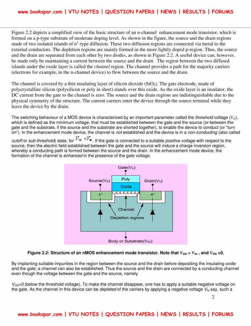
device is called a depletion mode device. Figure 2.3 shows the arrangement in a depletion mode MOS device. For an n-type depletion mode device, penta-valent impurities like phosphorus is used.
Figure 2.3 Structure of an nMOS depletion mode transistor
To describe the operation of an nMOS enhancement device, note that a positive voltage is applied between the source and the drain (VDS ). No current flows from the source and the drain at a zero gate bias (that is, VGS= 0). This is because the source and the drain are insulated from each other by the two reverse-biased diodes as shown in Figure 2.2.However, as a voltage, positive relative to the source and the substrate, is applied to the gate, an electric field is produced across the p-type substrate, This electric field attracts the electrons toward the gate and repels the holes. If the gate voltage is adequately high, the region under the gate changes from p-type to n-type, and it provides a conduction path between the source and the drain. A very thin surface of the p-type substrate is then said to be inverted, and the channel is said to be an n-channel.
To explain in more detail the electrical behaviour of the MOS structure under external bias, assume that the substrate voltage VSS = 0, and that the gate voltage VG is the controlling parameter. Three distinct operating regions, namely accumulation, depletion and inversion are identified based on polarity and magnitude of VG .
If a negative voltage VG is applied to the gate electrode, the holes in the p-type substrate are attracted towards the oxide-semiconductor interface. As the majority carrier (hole) concentration near the surface is larger than the equilibrium concentration in the substrate, this condition is referred to as the carrier accumulation on the surface. In this case, the oxide electric field is directed towards the gate electrode. Although the hole density increases near the surface in response to the negative gate bias, the minority carrier (electron) concentration goes down as the electrons are repelled deeper into the substrate.
Consider next the situation when a small positive voltage VG. is applied to the gate. The direction of the electric field across the oxide will now be towards the substrate. The holes (majority carriers) are now driven back into the substrate, leaving the negatively charged immobile acceptor ions. Lack of majority carriers create a depletion region near the surface. Almost no mobile carriers are found near the semiconductor-oxide interface under this bias condition.
Next, let us investigate the effect of further increase in the positive gate bias. At a voltage VGS = Vth , the region near the semiconductor surface acquires the properties of n-type material. This n-type surface layer however, is not due to any
www.bookspar.com | VTU NOTES | QUESTION PAPERS | NEWS | RESULTS | FORUMS
www.bookspar.com | VTU NOTES | QUESTION PAPERS | NEWS | RESULTS | FORUMS
4
doping operation, but rather by inversion of the originally p-type semiconductor owing to the applied voltage. This inverted layer, which is separated from the p-type substrate by a depletion region, accounts for the MOS transistor operation. That is, the thin inversion layer with a large mobile electron concentration, which is brought about by a sufficiently large positive voltage between the gate and the source, can be effectively used for conducting current between the source and the drain terminals of the MOS transistor. Strong inversion is said to occur when the concentration of the mobile electrons on the surface equals that of the holes in the underlying p-type substrate.
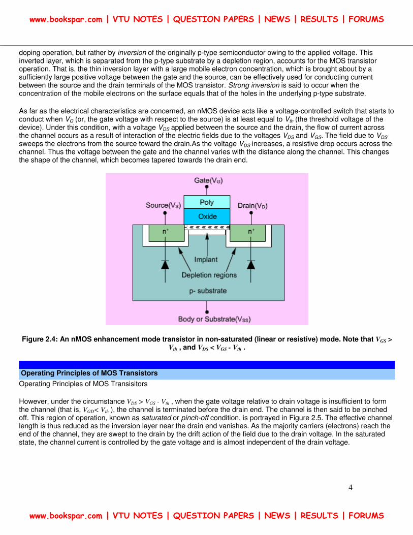
As far as the electrical characteristics are concerned, an nMOS device acts like a voltage-controlled switch that starts to conduct when VG (or, the gate voltage with respect to the source) is at least equal to Vth (the threshold voltage of the device). Under this condition, with a voltage VDS applied between the source and the drain, the flow of current across the channel occurs as a result of interaction of the electric fields due to the voltages VDS and VGS. The field due to VDS sweeps the electrons from the source toward the drain.As the voltage VDS increases, a resistive drop occurs across the channel. Thus the voltage between the gate and the channel varies with the distance along the channel. This changes the shape of the channel, which becomes tapered towards the drain end.
Figure 2.4: An nMOS enhancement mode transistor in non-saturated (linear or resistive) mode. Note that VGS >
Vth , and VDS < VGS - Vth .
Operating Principles of MOS Transistors
Operating Principles of MOS Transisitors
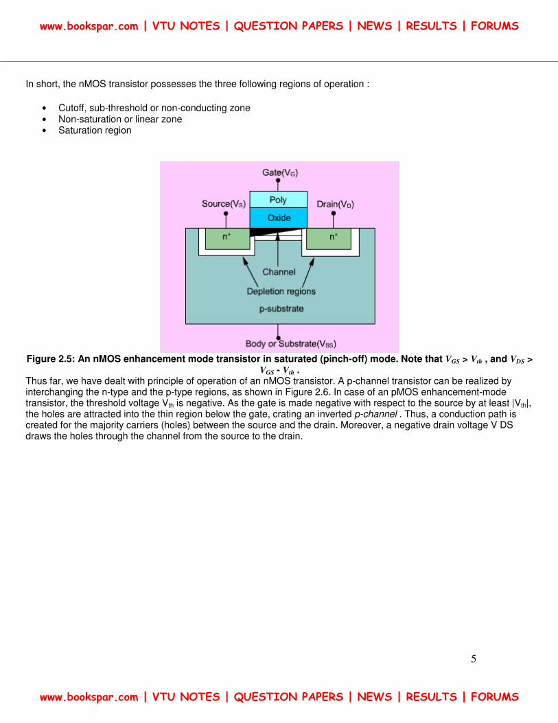
However, under the circumstance VDS > VGS - Vth , when the gate voltage relative to drain voltage is insufficient to form the channel (that is, VGD< Vth ), the channel is terminated before the drain end. The channel is then said to be pinched off. This region of operation, known as saturated or pinch-off condition, is portrayed in Figure 2.5. The effective channel length is thus reduced as the inversion layer near the drain end vanishes. As the majority carriers (electrons) reach the end of the channel, they are swept to the drain by the drift action of the field due to the drain voltage. In the saturated state, the channel current is controlled by the gate voltage and is almost independent of the drain voltage.
www.bookspar.com | VTU NOTES | QUESTION PAPERS | NEWS | RESULTS | FORUMS
www.bookspar.com | VTU NOTES | QUESTION PAPERS | NEWS | RESULTS | FORUMS
5
In short, the nMOS transistor possesses the three following regions of operation :
• Cutoff, sub-threshold or non-conducting zone • Non-saturation or linear zone • Saturation region
Figure 2.5: An nMOS enhancement mode transistor in saturated (pinch-off) mode. Note that VGS > Vth , and VDS >
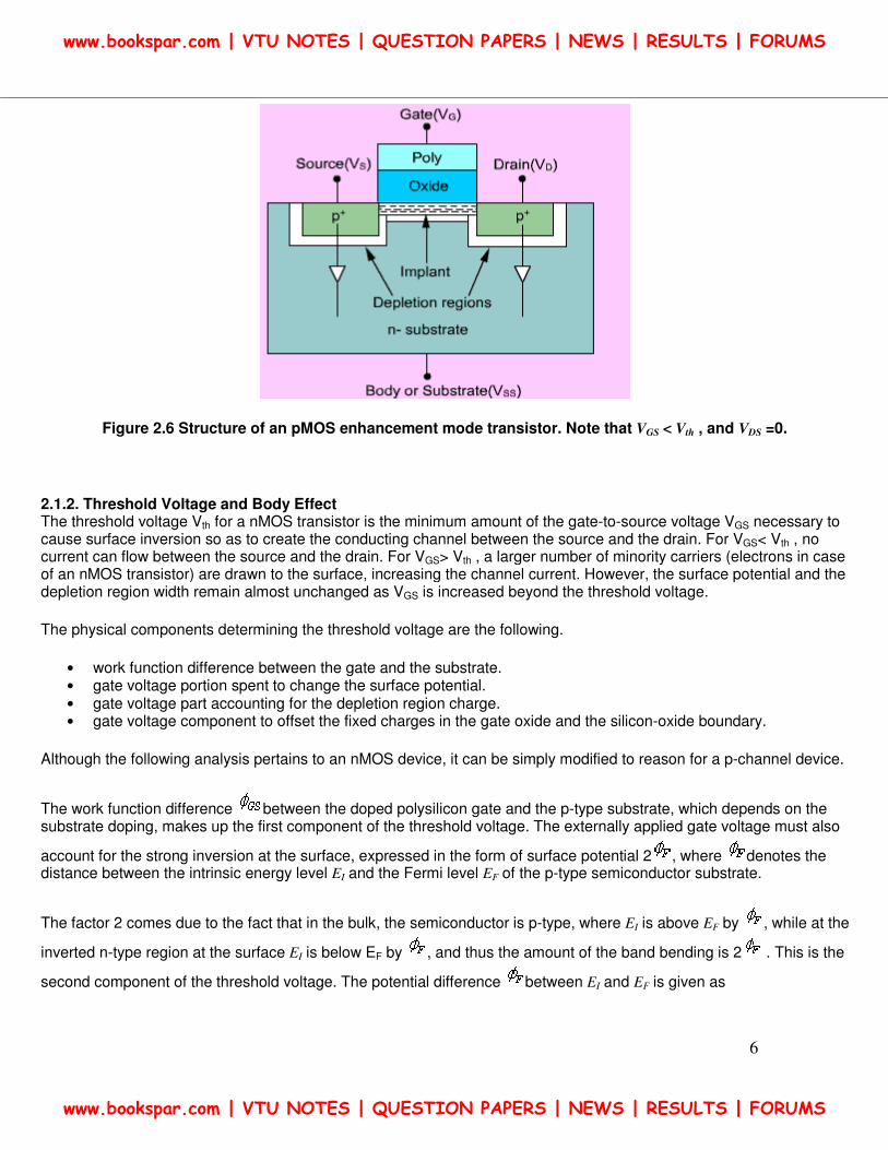
VGS - Vth . Thus far, we have dealt with principle of operation of an nMOS transistor. A p-channel transistor can be realized by interchanging the n-type and the p-type regions, as shown in Figure 2.6. In case of an pMOS enhancement-mode transistor, the threshold voltage Vth is negative. As the gate is made negative with respect to the source by at least |Vth|, the holes are attracted into the thin region below the gate, crating an inverted p-channel . Thus, a conduction path is created for the majority carriers (holes) between the source and the drain. Moreover, a negative drain voltage V DS draws the holes through the channel from the source to the drain.
www.bookspar.com | VTU NOTES | QUESTION PAPERS | NEWS | RESULTS | FORUMS
www.bookspar.com | VTU NOTES | QUESTION PAPERS | NEWS | RESULTS | FORUMS
6
Figure 2.6 Structure of an pMOS enhancement mode transistor. Note that VGS < Vth , and VDS =0.
2.1.2. Threshold Voltage and Body Effect The threshold voltage Vth for a nMOS transistor is the minimum amount of the gate-to-source voltage VGS necessary to cause surface inversion so as to create the conducting channel between the source and the drain. For VGS< Vth , no current can flow between the source and the drain. For VGS> Vth , a larger number of minority carriers (electrons in case of an nMOS transistor) are drawn to the surface, increasing the channel current. However, the surface potential and the depletion region width remain almost unchanged as VGS is increased beyond the threshold voltage.
The physical components determining the threshold voltage are the following.
• work function difference between the gate and the substrate. • gate voltage portion spent to change the surface potential. • gate voltage part accounting for the depletion region charge. • gate voltage component to offset the fixed charges in the gate oxide and the silicon-oxide boundary.
Although the following analysis pertains to an nMOS device, it can be simply modified to reason for a p-channel device.
The work function difference between the doped polysilicon gate and the p-type substrate, which depends on the substrate doping, makes up the first component of the threshold voltage. The externally applied gate voltage must also
account for the strong inversion at the surface, expressed in the form of surface potential 2 , where denotes the distance between the intrinsic energy level EI and the Fermi level EF of the p-type semiconductor substrate.
The factor 2 comes due to the fact that in the bulk, the semiconductor is p-type, where EI is above EF by , while at the
inverted n-type region at the surface EI is below EF by , and thus the amount of the band bending is 2 . This is the
second component of the threshold voltage. The potential difference between EI and EF is given as
www.bookspar.com | VTU NOTES | QUESTION PAPERS | NEWS | RESULTS | FORUMS
www.bookspar.com | VTU NOTES | QUESTION PAPERS | NEWS | RESULTS | FORUMS
7
where k: Boltzmann constant, T: temperature, q : electron charge NA : acceptor concentration in the p-substrate and n i : intrinsic carrier concentration. The expression kT/q is 0.02586 volt at 300 K.
The applied gate voltage must also be large enough to create the depletion charge. Note that the charge per unit area in the depletion region at strong inversion is given by
where is the substrate permittivity. If the source is biased at a potential VSB with respect to the substrate, then the depletion charge density is given by
The component of the threshold voltage that offsets the depletion charge is then given by -Qd /Cox , where Cox is the gate
oxide capacitance per unit area, or Cox = (ratio of the oxide permittivity and the oxide thickness).
A set of positive charges arises from the interface states at the Si-SiO2 interface. These charges, denoted as Qi , occur from the abrupt termination of the semiconductor crystal lattice at the oxide interface. The component of the gate voltage needed to offset this positive charge (which induces an equivalent negative charge in the semiconductor) is -Qi /Cox. On combining all the four voltage components, the threshold voltage VTO, for zero substrate bias, is expressed as
For non-zero substrate bias, however, the depletion charge density needs to be modified to include the effect of VSB on that charge, resulting in the following generalized expression for the threshold voltage, namely
The generalized form of the threshold voltage can also be written as
Note that the threshold voltage differs from VTO by an additive term due to substrate bias. This term, which depends on the material parameters and the source-to-substrate voltage VSB , is given by
www.bookspar.com | VTU NOTES | QUESTION PAPERS | NEWS | RESULTS | FORUMS
www.bookspar.com | VTU NOTES | QUESTION PAPERS | NEWS | RESULTS | FORUMS
8
Thus, in its most general form, the threshold voltage is determined as
........................... (2.1)
in which the parameter , known as the substrate-bias (or body-effect ) coefficient is given by
.................................... (2.2)
The threshold voltage expression given by (1.1) can be applied to n-channel as well as p-channel transistors. However, some of the parameters have opposite polarities for the pMOS and the nMOS transistors. For example, the substrate
bias voltage VSB is positive in nMOS and negative in pMOS devices. Also, the substrate potential difference is negative in nMOS, and positive in pMOS. Whereas, the body-effect coefficient is positive in nMOS and negative in pMOS. Typically, the threshold voltage of an enhancement mode n-channel transistor is positive, while that of a p-channel transistor is negative.
Example 2.1 Given the following parameters, namely the acceptor concentration of p-substrate NA =1016 cm-3 , polysilicon gate doping concentration N D =1016 cm-3 , intrinsic concentration of Si, ni =1.45 X 1010 cm-3 , gate oxide thickness tox =500 Å and oxide-interface fixed charge density Nox =4 X 1010cm-2 , calculate the threshold voltage VTO at VSB=0.
Ans:
The potential difference between EI and EF for the p-substrate is
For the polysilicon gate, as the doping concentration is extremely high, the heavily doped n-type gate material can be assumed to be degenerate. That is, the Fermi level EF is almost coincident with the bottom of the conduction band E C . Hence, assuming that the intrinsic energy level EI is at the middle of the band gap, the potential difference between EI
and EF for the gate is = ½ (energy band gap of Si) = 1/2 X 1.1 = 0.55 V.
Thus, the work function difference between the doped polysilicon gate and the p-type substrate is -0.35 V - 0.55 V = -0.90 V.
The depletion charge density at VSB =0 is
www.bookspar.com | VTU NOTES | QUESTION PAPERS | NEWS | RESULTS | FORUMS
www.bookspar.com | VTU NOTES | QUESTION PAPERS | NEWS | RESULTS | FORUMS
9
The oxide-interface charge density is
The gate oxide capacitance per unit area is (using dielectric constant of SiO2 as 3.97)
Combining the four components, the threshold voltage can now be computed as
Body Effect : The transistors in a MOS device seen so far are built on a common substrate. Thus, the substrate voltage of all such transistors are equal. However, while one designs a complex gate using MOS transistors, several devices may have to be connected in series. This will result in different source-to-substrate voltages for different devices. For example, in the NAND gate shown in Figure 1.5, the nMOS transistors are in series, whereby the source-to-substrate voltage VSB of the device corresponding to the input A is higher than that of the device for the input B.
Under normal conditions ( VGS > Vth ), the depletion layer width remains unchanged and the charge carriers are drawn into the channel from the source. As the substrate bias VSB is increased, the depletion layer width corresponding to the source-substrate field-induced junction also increases. This results in an increase in the density of the fixed charges in the depletion layer. For charge neutrality to be valid, the channel charge must go down. The consequence is that the substrate bias VSB gets added to the channel-substrate junction potential. This leads to an increase of the gate-channel voltage drop.
Example 2.2 Consider the n-channel MOS process in Example 2.1. One may examine how a non-zero source-to-substrate voltage VSB influences the threshold voltage of an nMOS transistor.
One can calculate the substrate-bias coefficient using the parameters provided in Example 2.1 as follows :
One is now in a position to determine the variation of threshold voltage VT as a function of the source-to-substrate voltage VSB . Assume the voltage VSB to range from 0 to 5 V.
www.bookspar.com | VTU NOTES | QUESTION PAPERS | NEWS | RESULTS | FORUMS
www.bookspar.com | VTU NOTES | QUESTION PAPERS | NEWS | RESULTS | FORUMS
10
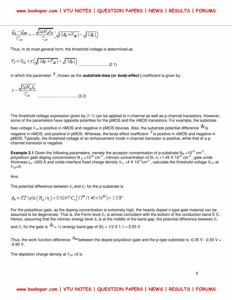
Figure 2.7 Variation of Threshold voltage in response to change in source-to-substrate voltage VSB
Figure 2.7 depicts the manner in which the threshold voltage Vth varies as a function of the source-to-substrate voltage VSB . As may be seen from the figure, the extent of the variation of the threshold voltage is nearly 1.3 Volts in this range. In most of the digital circuits, the substrate bias effect (also referred to as the body effect) is inevitable. Accordingly, appropriate measures have to be adopted to compensate for such variations in the threshold voltage.
2.2 MOS Device Current -Voltage Equations
This section first derives the current-voltage relationships for various bias conditions in a MOS transistor. Although the subsequent discussion is centred on an nMOS transistor, the basic expressions can be derived for a pMOS transistor
by simply replacing the electron mobility by the hole mobility and reversing the polarities of voltages and currents.
As mentioned in the earlier section, the fundamental operation of a MOS transistor arises out of the gate voltage VGS (between the gate and the source) creating a channel between the source and the drain, attracting the majority carriers from the source and causing them to move towards the drain under the influence of an electric field due to the voltage VDS (between the drain and the source). The corresponding current IDS depends on both VGS and VDS .
2.2.1 Basic DC Equations
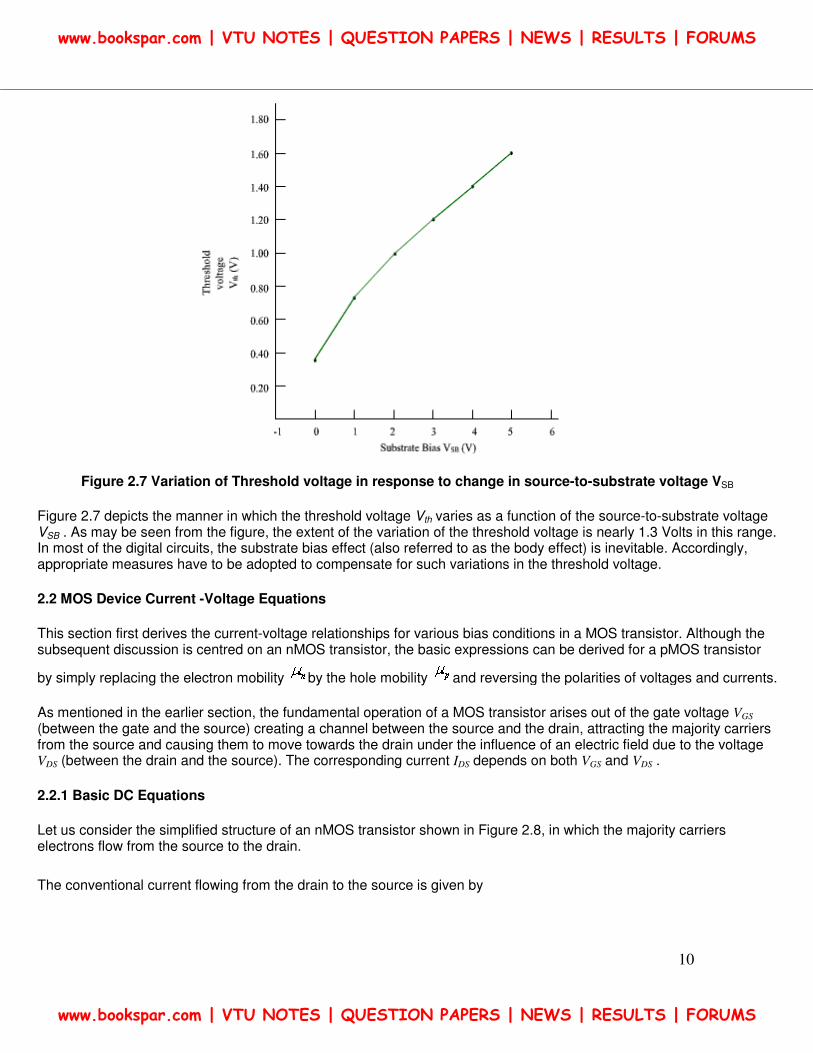
Let us consider the simplified structure of an nMOS transistor shown in Figure 2.8, in which the majority carriers electrons flow from the source to the drain.
The conventional current flowing from the drain to the source is given by
www.bookspar.com | VTU NOTES | QUESTION PAPERS | NEWS | RESULTS | FORUMS
www.bookspar.com | VTU NOTES | QUESTION PAPERS | NEWS | RESULTS | FORUMS
11
Now, transit time = ( length of the channel) / (electron velocity) = L / v
where velocity is given by the electron mobility and electric field; or,
Now, EDS = VDS/ L, so that velocity
Thus, the transit time is
At room temperature (300 K), typical values of the electron and hole mobility are given by
, and
We shall derive the current-voltage relationship separately for the linear (or non-saturated) region and the saturated region of operation.
Fig 2.8: Simplified geometrical structure of an nMOS transistor
Linear region : Note that this region of operation implies the existence of the uninterrupted channel between the source and the drain, which is ensured by the voltage relation VGS - Vth > VDS .
In the channel, the voltage between the gate and the varies linearly with the distance x from the source due to the IR drop in the channel. Assume that the device is not saturated and the average channel voltage is VDS /2.
The effective gate voltage VG,eff = Vgs - Vth
Charge per unit area =
www.bookspar.com | VTU NOTES | QUESTION PAPERS | NEWS | RESULTS | FORUMS
www.bookspar.com | VTU NOTES | QUESTION PAPERS | NEWS | RESULTS | FORUMS
12
where Eg average electric field from gate to channel, : relative permittivity of oxide between gate and channel (~4.0
for SiO2 ), and : free space permittivity (8.85 x 10 -14 F/cm). So, induced charge .
where W: width of the gate and L : length of channel.
Thus, the current from the drain to the source may be expressed as
Thus, in the non-saturated region, where
...........................(2.2)
where the parameter
Writing , where W/L is contributed by the geometry of the device,
.......................................(2.3)
Since, the gate-to-channel capacitance is (parallel plate capacitance), then
, so that (2.2) may be written as
.........................(2.4)
Denoting CG = C0 WL where C0 : gate capacitance per unit area,
...................... (2.5)
Saturated region : Under the voltage condition VGS - Vth = VDS , a MOS device is said to be in saturation region of operation. In fact, saturation begins when VDS = VGS - Vth , since at this point, the resistive voltage drop (IR drop) in the channel equals the effective gate-to-channel voltage at the drain. One may assume that the current remains constant as VDS increases further. Putting VDS = VGS - Vth , the equations (2.2-2.5) under saturation condition need to be modified as
www.bookspar.com | VTU NOTES | QUESTION PAPERS | NEWS | RESULTS | FORUMS
www.bookspar.com | VTU NOTES | QUESTION PAPERS | NEWS | RESULTS | FORUMS
13
...................................(2.6)
...................................................(2.7)
.....................................(2.8)
.......................................(2.9)
The expressions in the last slide derived for IDS are valid for both the enhancement and the depletion mode devices. However, the threshold voltage for the nMOS depletion mode devices (generally denoted as Vtd ) is negative .
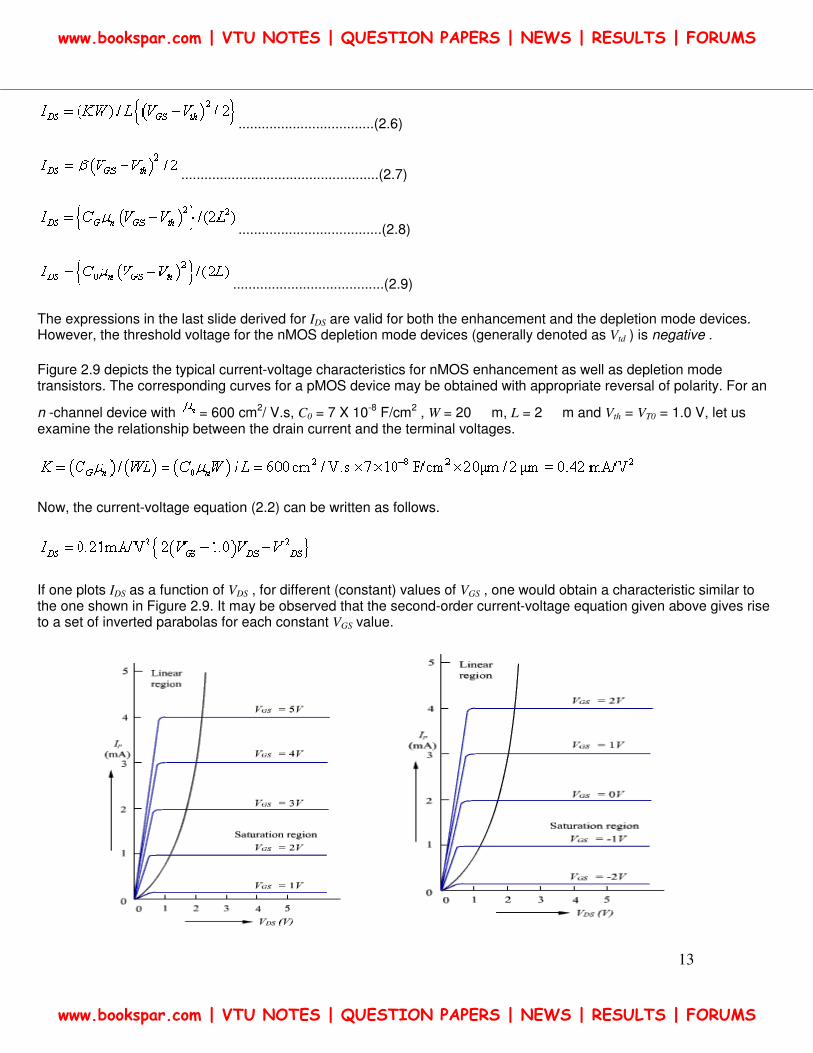
Figure 2.9 depicts the typical current-voltage characteristics for nMOS enhancement as well as depletion mode transistors. The corresponding curves for a pMOS device may be obtained with appropriate reversal of polarity. For an
n -channel device with = 600 cm2/ V.s, C0 = 7 X 10⁻⁸ F/cm2 , W = 20 m, L = 2 m and Vth = VT0 = 1.0 V, let us examine the relationship between the drain current and the terminal voltages.
Now, the current-voltage equation (2.2) can be written as follows.
If one plots IDS as a function of VDS , for different (constant) values of VGS , one would obtain a characteristic similar to the one shown in Figure 2.9. It may be observed that the second-order current-voltage equation given above gives rise to a set of inverted parabolas for each constant VGS value.
www.bookspar.com | VTU NOTES | QUESTION PAPERS | NEWS | RESULTS | FORUMS
www.bookspar.com | VTU NOTES | QUESTION PAPERS | NEWS | RESULTS | FORUMS
14
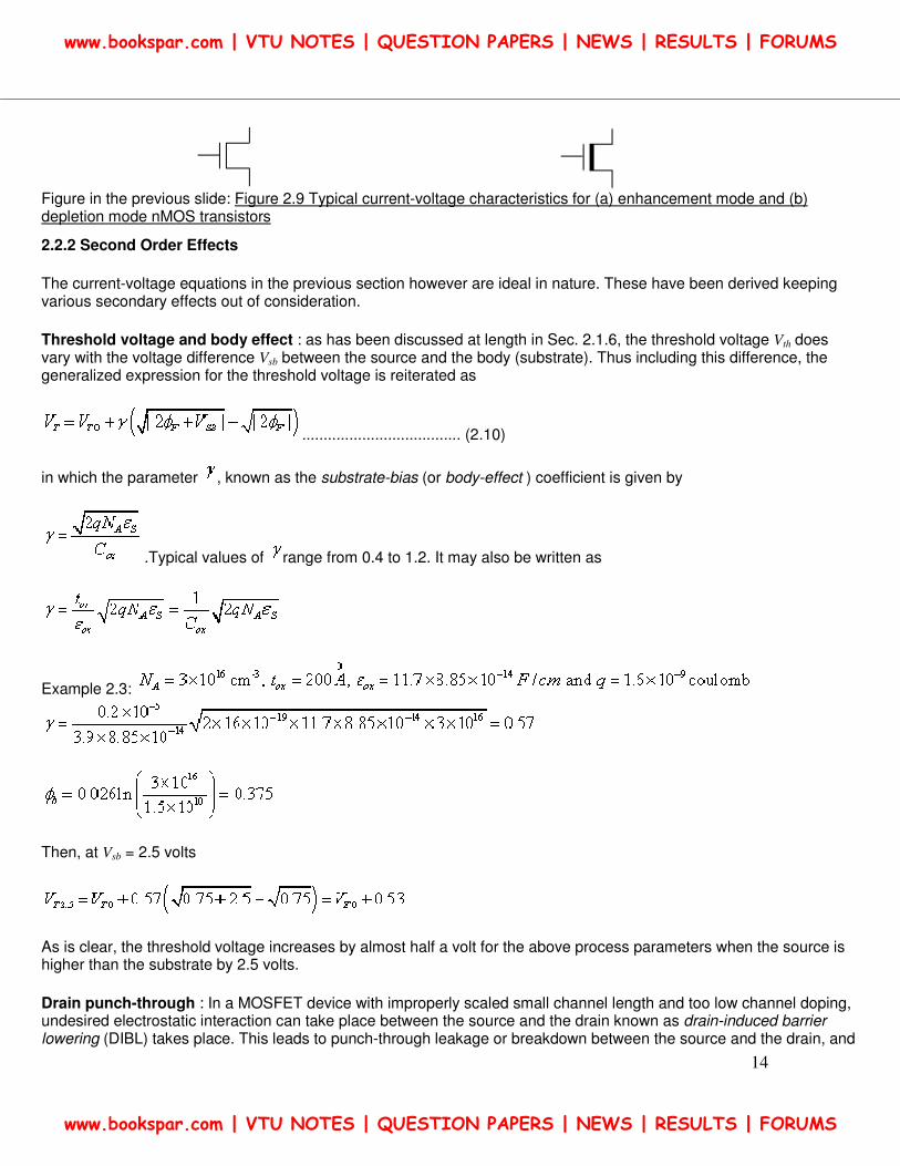
Figure in the previous slide: Figure 2.9 Typical current-voltage characteristics for (a) enhancement mode and (b) depletion mode nMOS transistors
2.2.2 Second Order Effects
The current-voltage equations in the previous section however are ideal in nature. These have been derived keeping various secondary effects out of consideration.
Threshold voltage and body effect : as has been discussed at length in Sec. 2.1.6, the threshold voltage Vth does vary with the voltage difference Vsb between the source and the body (substrate). Thus including this difference, the generalized expression for the threshold voltage is reiterated as
..................................... (2.10)
in which the parameter , known as the substrate-bias (or body-effect ) coefficient is given by
.Typical values of range from 0.4 to 1.2. It may also be written as
Example 2.3:
Then, at Vsb = 2.5 volts
As is clear, the threshold voltage increases by almost half a volt for the above process parameters when the source is higher than the substrate by 2.5 volts.
Drain punch-through : In a MOSFET device with improperly scaled small channel length and too low channel doping, undesired electrostatic interaction can take place between the source and the drain known as drain-induced barrier lowering (DIBL) takes place. This leads to punch-through leakage or breakdown between the source and the drain, and
www.bookspar.com | VTU NOTES | QUESTION PAPERS | NEWS | RESULTS | FORUMS
www.bookspar.com | VTU NOTES | QUESTION PAPERS | NEWS | RESULTS | FORUMS
15
loss of gate control. One should consider the surface potential along the channel to understand the punch-through phenomenon. As the drain bias increases, the conduction band edge (which represents the electron energies) in the drain is pulled down, leading to an increase in the drain-channel depletion width.
In a long-channel device, the drain bias does not influence the source-to-channel potential barrier, and it depends on the increase of gate bias to cause the drain current to flow. However, in a short-channel device, as a result of increase in drain bias and pull-down of the conduction band edge, the source-channel potential barrier is lowered due to DIBL. This in turn causes drain current to flow regardless of the gate voltage (that is, even if it is below the threshold voltage Vth). More simply, the advent of DIBL may be explained by the expansion of drain depletion region and its eventual merging with source depletion region, causing punch-through breakdown between the source and the drain. The punch-through condition puts a natural constraint on the voltages across the internal circuit nodes.
Sub-threshold region conduction : the cutoff region of operation is also referred to as the sub-threshold region, which is mathematically expressed as IDS =0 VGS < Vth
However, a phenomenon called sub-threshold conduction is observed in small-geometry transistors. The current flow in the channel depends on creating and maintaining an inversion layer on the surface. If the gate voltage is inadequate to invert the surface (that is, VGS< VT0 ), the electrons in the channel encounter a potential barrier that blocks the flow. However, in small-geometry MOSFETs, this potential barrier is controlled by both VGS and VDS . If the drain voltage is increased, the potential barrier in the channel decreases, leading to drain-induced barrier lowering (DIBL). The lowered potential barrier finally leads to flow of electrons between the source and the drain, even if VGS < VT0 (that is, even when the surface is not in strong inversion). The channel current flowing in this condition is called the sub-threshold current . This current, due mainly to diffusion between the source and the drain, is causing concern in deep sub-micron designs. The model implemented in SPICE brings in an exponential, semi-empirical dependence of the drain current on VGS in the weak inversion region. Defining a voltage V on as the boundary between the regions of weak and strong inversion,
www.bookspar.com | VTU NOTES | QUESTION PAPERS | NEWS | RESULTS | FORUMS
www.bookspar.com | VTU NOTES | QUESTION PAPERS | NEWS | RESULTS | FORUMS
16
where Ion is the current in strong inversion for VGS =Von .
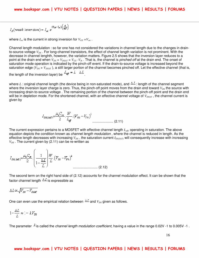
Channel length modulation : so far one has not considered the variations in channel length due to the changes in drain-to-source voltage VDS . For long-channel transistors, the effect of channel length variation is not prominent. With the decrease in channel lenghth, however, the variation matters. Figure 2.5 shows that the inversion layer reduces to a point at the drain end when VDS = VDSAT = VGS -Vth . That is, the channel is pinched off at the drain end. The onset of saturation mode operation is indicated by the pinch-off event. If the drain-to-source voltage is increased beyond the saturation edge (VDS > VDSAT ), a still larger portion of the channel becomes pinched off. Let the effective channel (that is,
the length of the inversion layer) be .
where L : original channel length (the device being in non-saturated mode), and : length of the channel segment where the inversion layer charge is zero. Thus, the pinch-off point moves from the drain end toward VDS the source with increasing drain-to-source voltage . The remaining portion of the channel between the pinch-off point and the drain end will be in depletion mode. For the shortened channel, with an effective channel voltage of VDSAT , the channel current is given by
...................... (2.11)
The current expression pertains to a MOSFET with effective channel length Leff, operating in saturation. The above equation depicts the condition known as channel length modulation , where the channel is reduced in length. As the effective length decreases with increasing VDS , the saturation current IDS(SAT) will consequently increase with increasing VDS . The current given by (2.11) can be re-written as
.......................... (2.12)
The second term on the right hand side of (2.12) accounts for the channel modulation effect. It can be shown that the factor channel length is expressible as
One can even use the empirical relation between and VDS given as follows.
The parameter is called the channel length modulation coefficient, having a value in the range 0.02V -1 to 0.005V -1 .
www.bookspar.com | VTU NOTES | QUESTION PAPERS | NEWS | RESULTS | FORUMS
www.bookspar.com | VTU NOTES | QUESTION PAPERS | NEWS | RESULTS | FORUMS
17
Assuming that , the saturation current given in (2.11) can be written as
The simplified equation (2.13) points to a linear dependence of the saturation current on the drain-to-source voltage. The slope of the current-voltage characteristic in the saturation region is determined by the channel length modulation
factor . Impact ionization :An electron traveling from the source to the drain along the channel gains kinetic energy at the cost of electrostatic potential energy in the pinch-off region, and becomes a “hot” electron. As the hot electrons travel towards the drain, they can create secondary electron-hole pairs by impact ionization. The secondary electrons are collected at the drain, and cause the drain current in saturation to increase with drain bias at high voltages, thus leading to a fall in the output impedance. The secondary holes are collected as substrate current. This effect is called impact ionization . The hot electrons can even penetrate the gate oxide, causing a gate current. This finally leads to degradation in MOSFET parameters like increase of threshold voltage and decrease of transconductance. Impact ionization can create circuit problems such as noise in mixed-signal systems, poor refresh times in dynamic memories, or latch-up in CMOS circuits. The remedy to this problem is to use a device with lightly doped drain. By reducing the doping density in the source/drain, the depletion width at the reverse-biased drain-channel junction is increase and consequently, the electric filed is reduced. Hot carrier effects do not normally present an acute problem for p -channel MOSFETs. This is because the channel mobility of holes is almost half that of the electrons. Thus, for the same filed, there are fewer hot holes than hot electrons. However, lower hole mobility results in lower drive currents in p -channel devices than in n -channel devices.
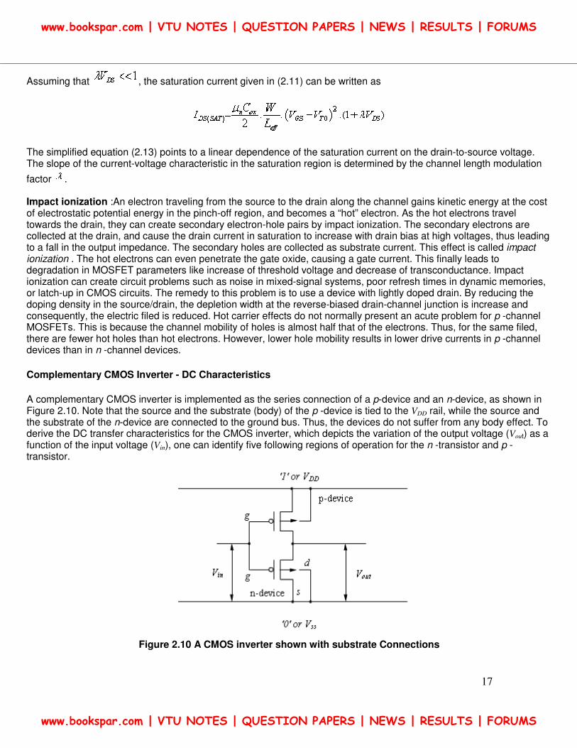
Complementary CMOS Inverter - DC Characteristics
A complementary CMOS inverter is implemented as the series connection of a p-device and an n-device, as shown in Figure 2.10. Note that the source and the substrate (body) of the p -device is tied to the VDD rail, while the source and the substrate of the n-device are connected to the ground bus. Thus, the devices do not suffer from any body effect. To derive the DC transfer characteristics for the CMOS inverter, which depicts the variation of the output voltage (Vout) as a function of the input voltage (Vin), one can identify five following regions of operation for the n -transistor and p -transistor.
Figure 2.10 A CMOS inverter shown with substrate Connections
www.bookspar.com | VTU NOTES | QUESTION PAPERS | NEWS | RESULTS | FORUMS
www.bookspar.com | VTU NOTES | QUESTION PAPERS | NEWS | RESULTS | FORUMS
18
Let Vtn and Vtp denote the threshold voltages of the n and p-devices respectively. The following voltages at the gate and the drain of the two devices (relative to their respective sources) are all referred with respect to the ground (or VSS), which is the substrate voltage of the n -device, namely
Vgsn =Vin , Vdsn =Vout, Vgsp =Vin -VDD , and Vdsp =Vout -VDD .
The voltage transfer characteristic of the CMOS inverter is now derived with reference to the following five regions of operation :
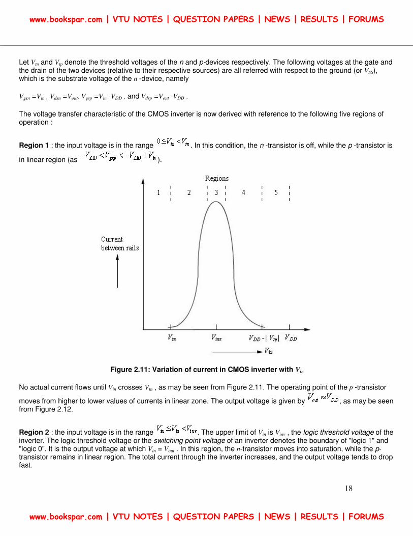
Region 1 : the input voltage is in the range . In this condition, the n -transistor is off, while the p -transistor is
in linear region (as ).
Figure 2.11: Variation of current in CMOS inverter with Vin
No actual current flows until Vin crosses Vtn , as may be seen from Figure 2.11. The operating point of the p -transistor
moves from higher to lower values of currents in linear zone. The output voltage is given by , as may be seen from Figure 2.12.
Region 2 : the input voltage is in the range . The upper limit of Vin is Vinv , the logic threshold voltage of the inverter. The logic threshold voltage or the switching point voltage of an inverter denotes the boundary of "logic 1" and "logic 0". It is the output voltage at which Vin = Vout . In this region, the n-transistor moves into saturation, while the p-transistor remains in linear region. The total current through the inverter increases, and the output voltage tends to drop fast.
www.bookspar.com | VTU NOTES | QUESTION PAPERS | NEWS | RESULTS | FORUMS
www.bookspar.com | VTU NOTES | QUESTION PAPERS | NEWS | RESULTS | FORUMS
19
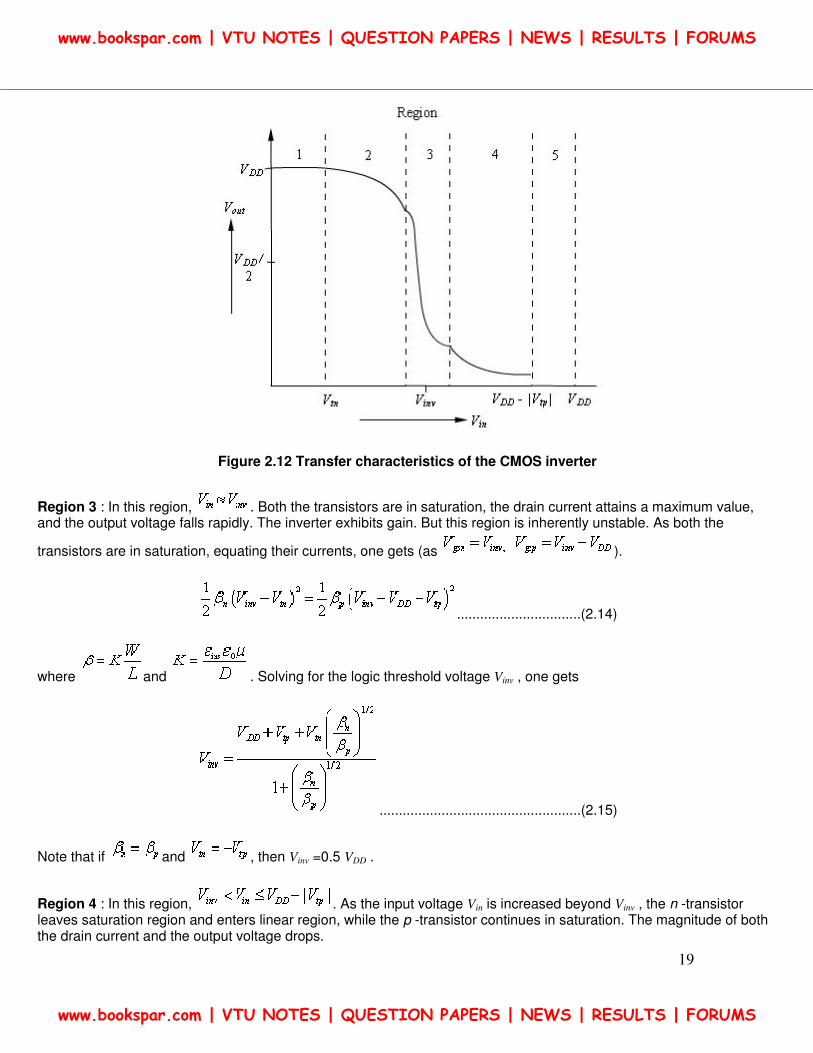
Figure 2.12 Transfer characteristics of the CMOS inverter
Region 3 : In this region, . Both the transistors are in saturation, the drain current attains a maximum value, and the output voltage falls rapidly. The inverter exhibits gain. But this region is inherently unstable. As both the
transistors are in saturation, equating their currents, one gets (as ).
................................(2.14)
where and . Solving for the logic threshold voltage Vinv , one gets
....................................................(2.15)
Note that if and , then Vinv =0.5 VDD .
Region 4 : In this region, . As the input voltage Vin is increased beyond Vinv , the n -transistor leaves saturation region and enters linear region, while the p -transistor continues in saturation. The magnitude of both the drain current and the output voltage drops.
www.bookspar.com | VTU NOTES | QUESTION PAPERS | NEWS | RESULTS | FORUMS
www.bookspar.com | VTU NOTES | QUESTION PAPERS | NEWS | RESULTS | FORUMS
20
Region 5 : In this region, . At this point, the p -transistor is turned off, and the n -transistor is in linear region, drawing a small current, which falls to zero as Vin increases beyond VDD -| Vtp|, since the p -transistor turns
off the current path. The output in this region is .
As may be seen from the transfer curve in Figure 2.12, the transition from "logic 1" state (represented by regions 1 and 2) to “logic 0” state (represented by regions 4 and 5) is quite steep. This characteristic guarantees maximum noise immunity.
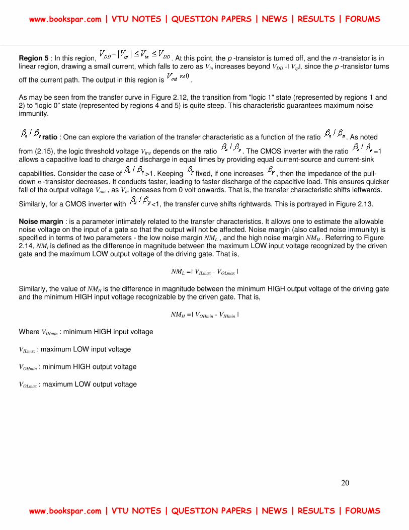
ratio : One can explore the variation of the transfer characteristic as a function of the ratio . As noted
from (2.15), the logic threshold voltage Vinv depends on the ratio . The CMOS inverter with the ratio =1 allows a capacitive load to charge and discharge in equal times by providing equal current-source and current-sink
capabilities. Consider the case of >1. Keeping fixed, if one increases , then the impedance of the pull-down n -transistor decreases. It conducts faster, leading to faster discharge of the capacitive load. This ensures quicker fall of the output voltage Vout , as Vin increases from 0 volt onwards. That is, the transfer characteristic shifts leftwards.
Similarly, for a CMOS inverter with <1, the transfer curve shifts rightwards. This is portrayed in Figure 2.13.
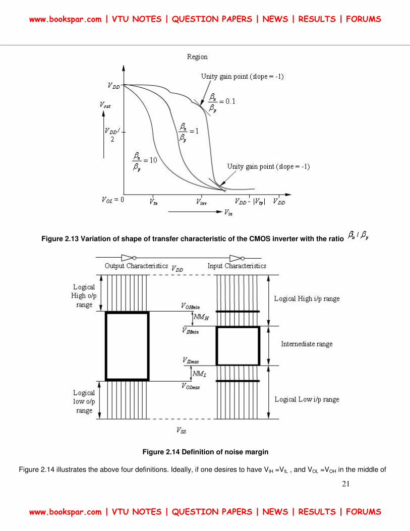
Noise margin : is a parameter intimately related to the transfer characteristics. It allows one to estimate the allowable noise voltage on the input of a gate so that the output will not be affected. Noise margin (also called noise immunity) is specified in terms of two parameters - the low noise margin NML , and the high noise margin NMH . Referring to Figure 2.14, NMl is defined as the difference in magnitude between the maximum LOW input voltage recognized by the driven gate and the maximum LOW output voltage of the driving gate. That is,
NML =| VILmax - VOLmax |
Similarly, the value of NMH is the difference in magnitude between the minimum HIGH output voltage of the driving gate and the minimum HIGH input voltage recognizable by the driven gate. That is,
NMH =| VOHmin - VIHmin |
Where VIHmin : minimum HIGH input voltage
VILmax : maximum LOW input voltage
VOHmin : minimum HIGH output voltage
VOLmax : maximum LOW output voltage
www.bookspar.com | VTU NOTES | QUESTION PAPERS | NEWS | RESULTS | FORUMS
www.bookspar.com | VTU NOTES | QUESTION PAPERS | NEWS | RESULTS | FORUMS
21
Figure 2.13 Variation of shape of transfer characteristic of the CMOS inverter with the ratio
Figure 2.14 Definition of noise margin
Figure 2.14 illustrates the above four definitions. Ideally, if one desires to have VIH =VIL , and VOL =VOH in the middle of
www.bookspar.com | VTU NOTES | QUESTION PAPERS | NEWS | RESULTS | FORUMS
www.bookspar.com | VTU NOTES | QUESTION PAPERS | NEWS | RESULTS | FORUMS
22
the logic swing, then the switching of states should be abtrupt, which in turn requires very high gain in the transition region. To calculate VIL , the inverter is supposed to be in region 2 (referring to Figure 2.12) of operation, where the p -transistor is in linear zone while the n -transistor is in saturation. The parameter VIL is found out by considering the unity gain point on the inverter transfer characteristic where the output makes a transition from VOH . Similarly, the parameter VIH is found by considering the unity gain point at the VOL end of the characteristic.
If the noise margins NMH or NML are reduced to a low value, then the gate may be susceptible to switching noise that may be present at the inputs. The net effect of noise sources and noise margins on cascaded gates must be considered in estimating the overall noise immunity of a particular system. Not infrequently, noise margins are compromised to improve speed.
CMOS inverter as an amplifier : In the region 3 (referring to Figure 2.12) of operation, the inverter actually acts as an analog amplifier where both the transistors are in saturation. The input-output behaviour of the inverter in this region is given by
Vout = AVin
where A is the stage gain given by
A = (gmn + gmp ) (rdsn || rdsp )
Note that the small-signal characteristics, namely transconductance gm is defined as
and the output resistance rds is given by
Note that the gain A is dependent on the process and the transistors used in the circuit. It can be increased by increasing the length of the transistors to improve the output resistance. However, speed and bandwidth of the amplifier suffer as a result.
Amplifiers with Active Loads – CMOS Amplifiers
Section 3.1 Amplifiers with Active Loads
www.bookspar.com | VTU NOTES | QUESTION PAPERS | NEWS | RESULTS | FORUMS
www.bookspar.com | VTU NOTES | QUESTION PAPERS | NEWS | RESULTS | FORUMS
23
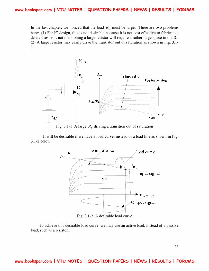
In the last chapter, we noticed that the load LR must be large. There are two problems
here: (1) For IC design, this is not desirable because it is not cost effective to fabricate a
desired resistor, not mentioning a large resistor will require a rather large space in the IC.
(2) A large resistor may easily drive the transistor out of saturation as shown in Fig. 3.1-
1.
Fig. 3.1-1 A large LR driving a transition out of saturation
It will be desirable if we have a load curve, instead of a load line as shown in Fig.
3.1-2 below:
Fig. 3.1-2 A desirable load curve
To achieve this desirable load curve, we may use an active load, instead of a passive
load, such as a resistor.
www.bookspar.com | VTU NOTES | QUESTION PAPERS | NEWS | RESULTS | FORUMS
www.bookspar.com | VTU NOTES | QUESTION PAPERS | NEWS | RESULTS | FORUMS
24
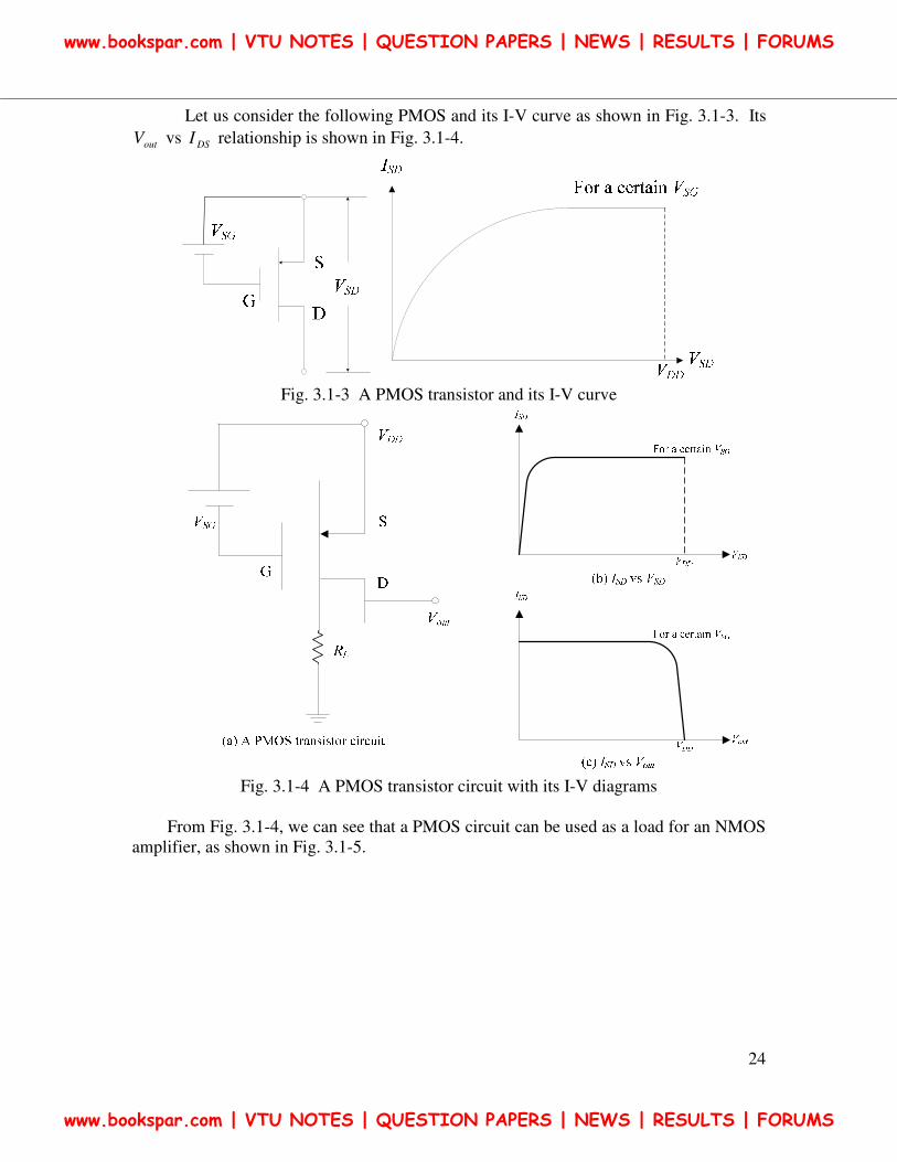
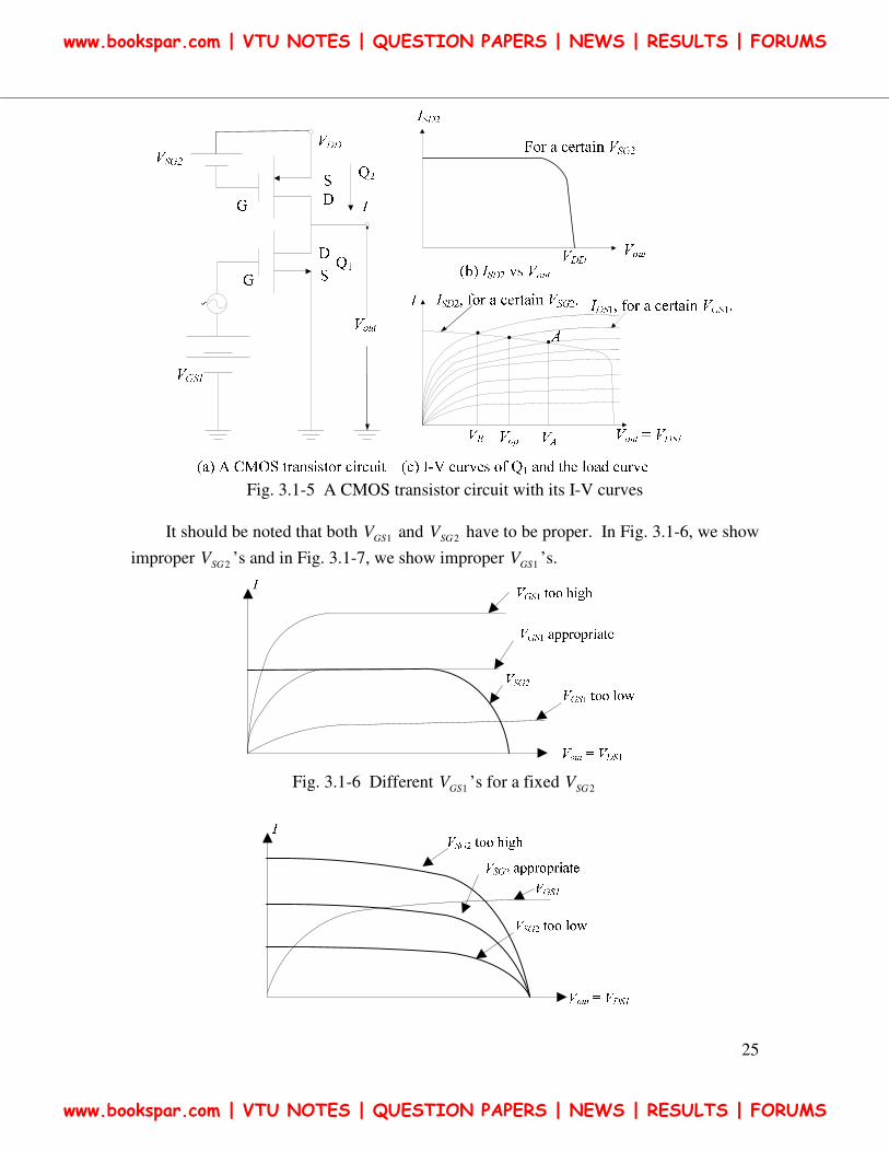
Let us consider the following PMOS and its I-V curve as shown in Fig. 3.1-3. Its
outV vs DSI relationship is shown in Fig. 3.1-4.
Fig. 3.1-3 A PMOS transistor and its I-V curve
Fig. 3.1-4 A PMOS transistor circuit with its I-V diagrams
From Fig. 3.1-4, we can see that a PMOS circuit can be used as a load for an NMOS
amplifier, as shown in Fig. 3.1-5.
www.bookspar.com | VTU NOTES | QUESTION PAPERS | NEWS | RESULTS | FORUMS
www.bookspar.com | VTU NOTES | QUESTION PAPERS | NEWS | RESULTS | FORUMS
25
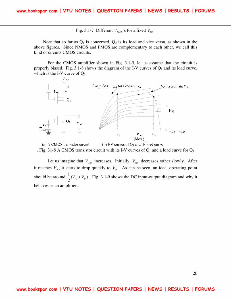
Fig. 3.1-5 A CMOS transistor circuit with its I-V curves
It should be noted that both 1GSV and 2SGV have to be proper. In Fig. 3.1-6, we show
improper 2SGV ’s and in Fig. 3.1-7, we show improper 1GSV ’s.
Fig. 3.1-6 Different 1GSV ’s for a fixed 2SGV
www.bookspar.com | VTU NOTES | QUESTION PAPERS | NEWS | RESULTS | FORUMS
www.bookspar.com | VTU NOTES | QUESTION PAPERS | NEWS | RESULTS | FORUMS
26
Fig. 3.1-7 Different 2SGV ’s for a fixed 1GSV
Note that so far as Q1 is concerned, Q2 is its load and vice versa, as shown in the
above figures. Since NMOS and PMOS are complementary to each other, we call this
kind of circuits CMOS circuits.
For the CMOS amplifier shown in Fig. 3.1-5, let us assume that the circuit is
properly biased. Fig. 3.1-8 shows the diagram of the I-V curves of Q1 and its load curve,
which is the I-V curve of Q2.
. Fig. 31-8 A CMOS transistor circuit with its I-V curves of Q1 and a load curve for Q1
Let us imagine that 1GSV increases. Initially, outV decreases rather slowly. After
it reaches AV , it starts to drop quickly to BV . As can be seen, an ideal operating point
should be around )(2
1BA VV + . Fig. 3.1-9 shows the DC input-output diagram and why it
behaves as an amplifier..
www.bookspar.com | VTU NOTES | QUESTION PAPERS | NEWS | RESULTS | FORUMS
www.bookspar.com | VTU NOTES | QUESTION PAPERS | NEWS | RESULTS | FORUMS
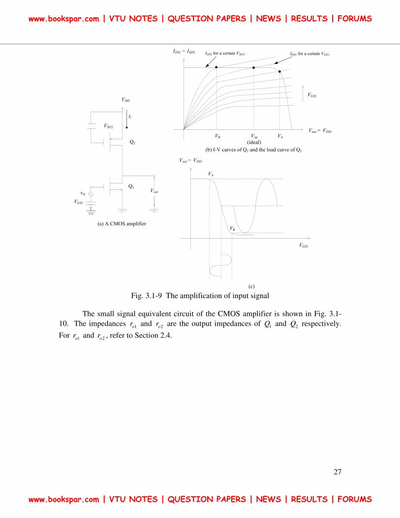
27
IDS1 = ISD2
Vout = VDS1VAVop
(ideal)
VB
VGS1
IDS1 for a certain VGS1.ISD2 for a certain VSG2.
Vout = VDS1
VGS1
VA
VB
Vout
VDD
Q2
Q1
I2
AC
VGS1
vin
VSG2
(b) I-V curves of Q1 and the load curve of Q1
(a) A CMOS amplifier
(c) Fig. 3.1-9 The amplification of input signal
The small signal equivalent circuit of the CMOS amplifier is shown in Fig. 3.1-
10. The impedances 1or and 2o
r are the output impedances of 1Q and 2Q respectively.
For 1or and 2o
r , refer to Section 2.4.
www.bookspar.com | VTU NOTES | QUESTION PAPERS | NEWS | RESULTS | FORUMS
www.bookspar.com | VTU NOTES | QUESTION PAPERS | NEWS | RESULTS | FORUMS
28
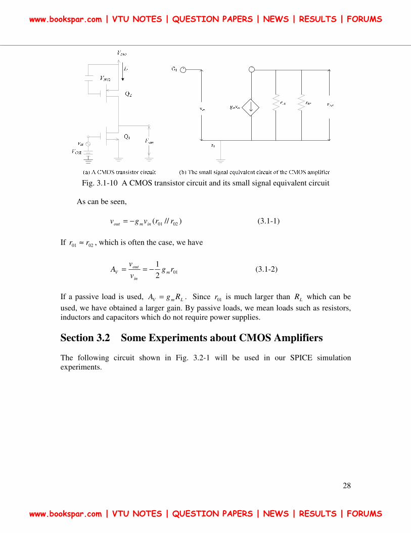
Fig. 3.1-10 A CMOS transistor circuit and its small signal equivalent circuit
As can be seen,
)//( 0201 rrvgv inmout −= (3.1-1)
If 0201 rr ≈ , which is often the case, we have
012
1rg
v
vA m
in
out
V −== (3.1-2)
If a passive load is used, LmV RgA = . Since 01r is much larger than LR which can be
used, we have obtained a larger gain. By passive loads, we mean loads such as resistors,
inductors and capacitors which do not require power supplies.
Section 3.2 Some Experiments about CMOS Amplifiers
The following circuit shown in Fig. 3.2-1 will be used in our SPICE simulation
experiments.
www.bookspar.com | VTU NOTES | QUESTION PAPERS | NEWS | RESULTS | FORUMS
www.bookspar.com | VTU NOTES | QUESTION PAPERS | NEWS | RESULTS | FORUMS
29
Fig. 3.2-1 The CMOS amplifier circuit for the Experiments in Section 3.2
Experiment 3.2-1. The I-V Curve of Q1 and the its Load Curve.
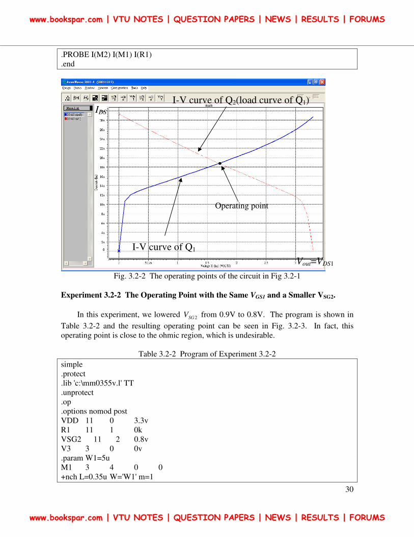
In Table 3.2-1, we display the SPICE simulation program of the experiment and in Fig.
3.2-2, we show the I-V curve of Q1 and its load curve. Note that the load curve of Q1 is
the I-V curve of Q2.
Table 3.2-1 Program of Experiment 3.2-1
simple
.protect
.lib 'c:\mm0355v.l' TT
.unprotect
.op
.options nomod post
VDD 11 0 3.3v
R1 11 1 0k
VSG2 11 2 0.9v
V3 3 0 0v
.param W1=5u
M1 3 4 0 0
+nch L=0.35u W='W1' m=1
+AD='0.95u*W1' PD='2*(0.95u+W1)'
+AS='0.95u*W1' PS='2*(0.95u+W1)'
M2 3 2 1 1
+pch L=0.35u W='W1' m=1
+AD='0.95u*W1' PD='2*(0.95u+W1)'
+AS='0.95u*W1' PS='2*(0.95u+W1)'
VGS1 4 0 0.65v
.DC V3 0 3.3v 0.1v
www.bookspar.com | VTU NOTES | QUESTION PAPERS | NEWS | RESULTS | FORUMS
www.bookspar.com | VTU NOTES | QUESTION PAPERS | NEWS | RESULTS | FORUMS
30
.PROBE I(M2) I(M1) I(R1)
.end
Fig. 3.2-2 The operating points of the circuit in Fig 3.2-1
Experiment 3.2-2 The Operating Point with the Same VGS1 and a Smaller VSG2.
In this experiment, we lowered 2SGV from 0.9V to 0.8V. The program is shown in
Table 3.2-2 and the resulting operating point can be seen in Fig. 3.2-3. In fact, this
operating point is close to the ohmic region, which is undesirable.
Table 3.2-2 Program of Experiment 3.2-2
simple
.protect
.lib 'c:\mm0355v.l' TT
.unprotect
.op
.options nomod post
VDD 11 0 3.3v
R1 11 1 0k
VSG2 11 2 0.8v
V3 3 0 0v
.param W1=5u
M1 3 4 0 0
+nch L=0.35u W='W1' m=1
Vout=VDS1
IDS
Operating point
I-V curve of Q2(load curve of Q1)
I-V curve of Q1
www.bookspar.com | VTU NOTES | QUESTION PAPERS | NEWS | RESULTS | FORUMS
www.bookspar.com | VTU NOTES | QUESTION PAPERS | NEWS | RESULTS | FORUMS
31
+AD='0.95u*W1' PD='2*(0.95u+W1)'
+AS='0.95u*W1' PS='2*(0.95u+W1)'
M2 3 2 1 1
+pch L=0.35u W='W1' m=1
+AD='0.95u*W1' PD='2*(0.95u+W1)'
+AS='0.95u*W1' PS='2*(0.95u+W1)'
VGS1 4 0 0.65v
.DC V3 0 3.3v 0.1v
.PROBE I(M2) I(M1) I(R1)
.end
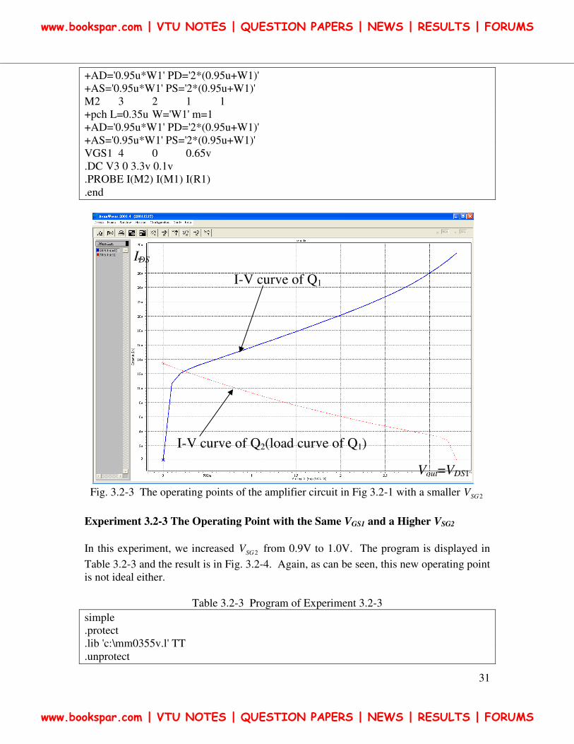
Fig. 3.2-3 The operating points of the amplifier circuit in Fig 3.2-1 with a smaller 2SGV
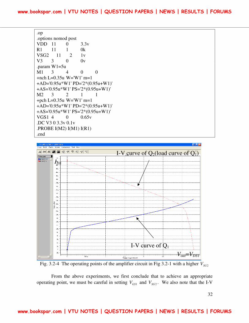
Experiment 3.2-3 The Operating Point with the Same VGS1 and a Higher VSG2
In this experiment, we increased 2SGV from 0.9V to 1.0V. The program is displayed in
Table 3.2-3 and the result is in Fig. 3.2-4. Again, as can be seen, this new operating point
is not ideal either.
Table 3.2-3 Program of Experiment 3.2-3
simple
.protect
.lib 'c:\mm0355v.l' TT
.unprotect
Vout=VDS1
IDS
I-V curve of Q2(load curve of Q1)
I-V curve of Q1
www.bookspar.com | VTU NOTES | QUESTION PAPERS | NEWS | RESULTS | FORUMS
www.bookspar.com | VTU NOTES | QUESTION PAPERS | NEWS | RESULTS | FORUMS
32
.op
.options nomod post
VDD 11 0 3.3v
R1 11 1 0k
VSG2 11 2 1v
V3 3 0 0v
.param W1=5u
M1 3 4 0 0
+nch L=0.35u W='W1' m=1
+AD='0.95u*W1' PD='2*(0.95u+W1)'
+AS='0.95u*W1' PS='2*(0.95u+W1)'
M2 3 2 1 1
+pch L=0.35u W='W1' m=1
+AD='0.95u*W1' PD='2*(0.95u+W1)'
+AS='0.95u*W1' PS='2*(0.95u+W1)'
VGS1 4 0 0.65v
.DC V3 0 3.3v 0.1v
.PROBE I(M2) I(M1) I(R1)
.end
Fig. 3.2-4 The operating points of the amplifier circuit in Fig 3.2-1 with a higher 2SGV
From the above experiments, we first conclude that to achieve an appropriate
operating point, we must be careful in setting 1GSV and 2SGV . We also note that the I-V
Vout=VDS1
IDS
I-V curve of Q2(load curve of Q1)
I-V curve of Q1
www.bookspar.com | VTU NOTES | QUESTION PAPERS | NEWS | RESULTS | FORUMS
www.bookspar.com | VTU NOTES | QUESTION PAPERS | NEWS | RESULTS | FORUMS
33
curves are not so flat as we wished. Therefore, we cannot expect a very high gain with
this kind of simple CMOS circuits. As we shall learn in later chapters, the gain can be
higher if we use a cascode design.
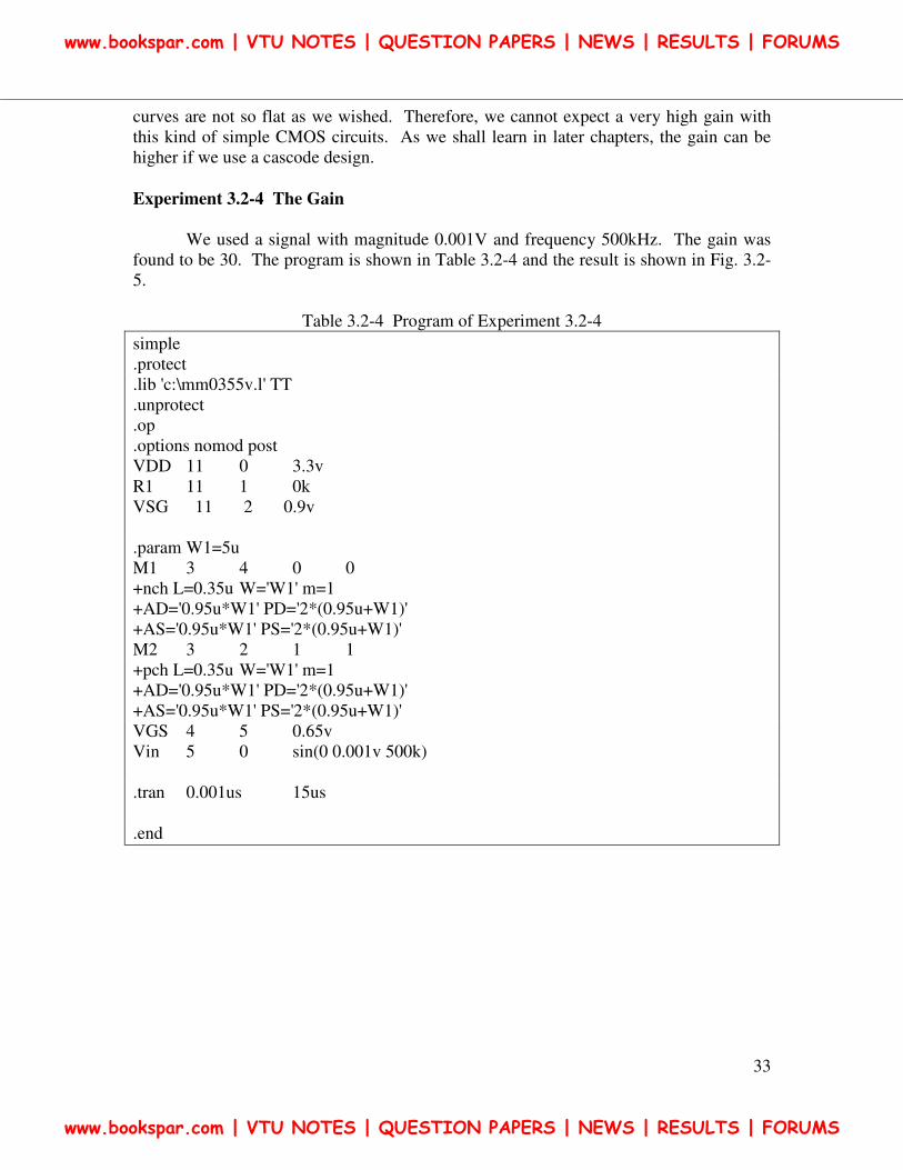
Experiment 3.2-4 The Gain
We used a signal with magnitude 0.001V and frequency 500kHz. The gain was
found to be 30. The program is shown in Table 3.2-4 and the result is shown in Fig. 3.2-
5.
Table 3.2-4 Program of Experiment 3.2-4
simple
.protect
.lib 'c:\mm0355v.l' TT
.unprotect
.op
.options nomod post
VDD 11 0 3.3v
R1 11 1 0k
VSG 11 2 0.9v
.param W1=5u
M1 3 4 0 0
+nch L=0.35u W='W1' m=1
+AD='0.95u*W1' PD='2*(0.95u+W1)'
+AS='0.95u*W1' PS='2*(0.95u+W1)'
M2 3 2 1 1
+pch L=0.35u W='W1' m=1
+AD='0.95u*W1' PD='2*(0.95u+W1)'
+AS='0.95u*W1' PS='2*(0.95u+W1)'
VGS 4 5 0.65v
Vin 5 0 sin(0 0.001v 500k)
.tran 0.001us 15us
.end
www.bookspar.com | VTU NOTES | QUESTION PAPERS | NEWS | RESULTS | FORUMS
www.bookspar.com | VTU NOTES | QUESTION PAPERS | NEWS | RESULTS | FORUMS
34
Fig. 3.2-5 The gain of the CMOS amplifier for input signal with 500KHz
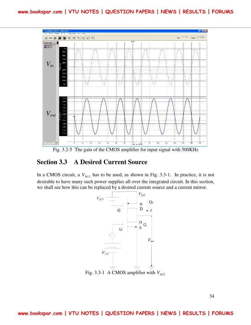
Section 3.3 A Desired Current Source
In a CMOS circuit, a 2SGV has to be used, as shown in Fig. 3.3-1. In practice, it is not
desirable to have many such power supplies all over the integrated circuit. In this section,
we shall see how this can be replaced by a desired current source and a current mirror.
Fig. 3.3-1 A CMOS amplifier with 2SGV
Vin
Vout
www.bookspar.com | VTU NOTES | QUESTION PAPERS | NEWS | RESULTS | FORUMS
www.bookspar.com | VTU NOTES | QUESTION PAPERS | NEWS | RESULTS | FORUMS
35
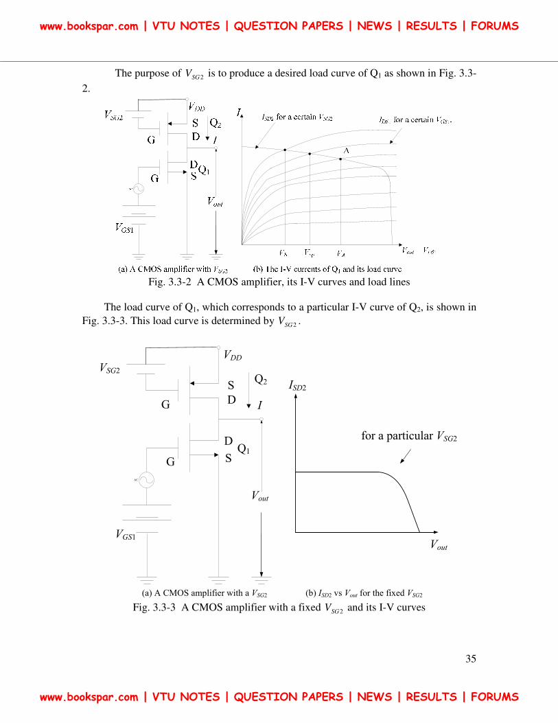
The purpose of 2SGV is to produce a desired load curve of Q1 as shown in Fig. 3.3-
2.
Fig. 3.3-2 A CMOS amplifier, its I-V curves and load lines
The load curve of Q1, which corresponds to a particular I-V curve of Q2, is shown in
Fig. 3.3-3. This load curve is determined by 2SGV .
AC
VSG2
VGS1
G
G
S
D
Vout
S
D
VDD
I
Q2
Q1
Vout
ISD2
for a particular VSG2
(a) A CMOS amplifier with a VSG2 (b) ISD2 vs Vout for the fixed VSG2 Fig. 3.3-3 A CMOS amplifier with a fixed 2SGV and its I-V curves
www.bookspar.com | VTU NOTES | QUESTION PAPERS | NEWS | RESULTS | FORUMS
www.bookspar.com | VTU NOTES | QUESTION PAPERS | NEWS | RESULTS | FORUMS
36
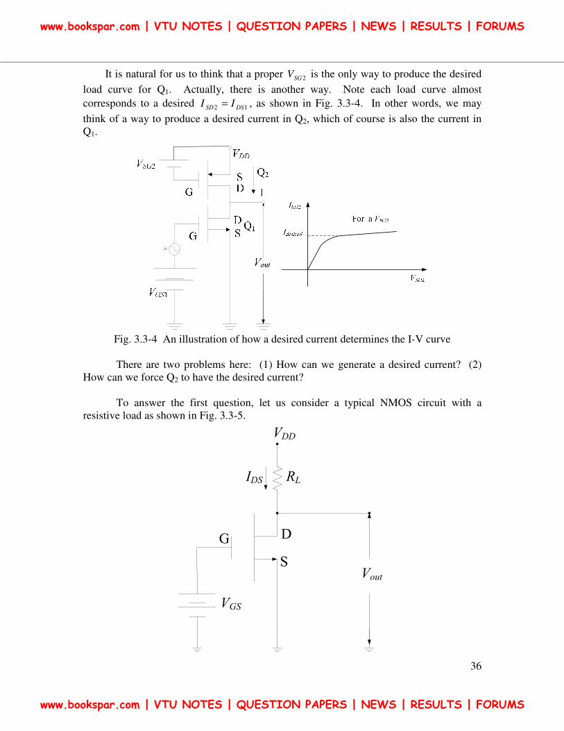
It is natural for us to think that a proper 2SGV is the only way to produce the desired
load curve for Q1. Actually, there is another way. Note each load curve almost
corresponds to a desired 12 DSSD II = , as shown in Fig. 3.3-4. In other words, we may
think of a way to produce a desired current in Q2, which of course is also the current in
Q1.
Fig. 3.3-4 An illustration of how a desired current determines the I-V curve
There are two problems here: (1) How can we generate a desired current? (2)
How can we force Q2 to have the desired current?
To answer the first question, let us consider a typical NMOS circuit with a
resistive load as shown in Fig. 3.3-5.
VGS
S
DG
RL
VDD
IDS
Vout
www.bookspar.com | VTU NOTES | QUESTION PAPERS | NEWS | RESULTS | FORUMS
www.bookspar.com | VTU NOTES | QUESTION PAPERS | NEWS | RESULTS | FORUMS
37
Fig. 3.3-5 An NMOS circuit with a resistive load
In the ohmic region, the relationship between the current DSI and different voltages
is expressed as below:
)2
1)(('
2
DSDStGSnDS VVVVL
WkI −−
= (3.3-1)
L
DSDD
DSR
VVI
−= (3.3-2)
Suppose we want to have a desired current DSI . We may think that DSI is a constant.
But, from the above equations, we still have three variables, namely DSGS VV , and .LR
Since there are only two equations, we cannot find these three variables for a given
desired DSI .
In the boundary between ohmic and saturation regions where tGSDS VVV −= , the
two equations governing current and voltages in the transistor are as follows:
2)('2
1tGSnDS VV
L
WkI −
= (3.3-3)
and L
DSDD
DSR
VVI
−= (3.3-4)
As can be seen, there are still three variables and only two equations.
There is a trick to solve the above problem. We may connect the drain to gate as
shown in Fig. 3.3-6.
www.bookspar.com | VTU NOTES | QUESTION PAPERS | NEWS | RESULTS | FORUMS
www.bookspar.com | VTU NOTES | QUESTION PAPERS | NEWS | RESULTS | FORUMS
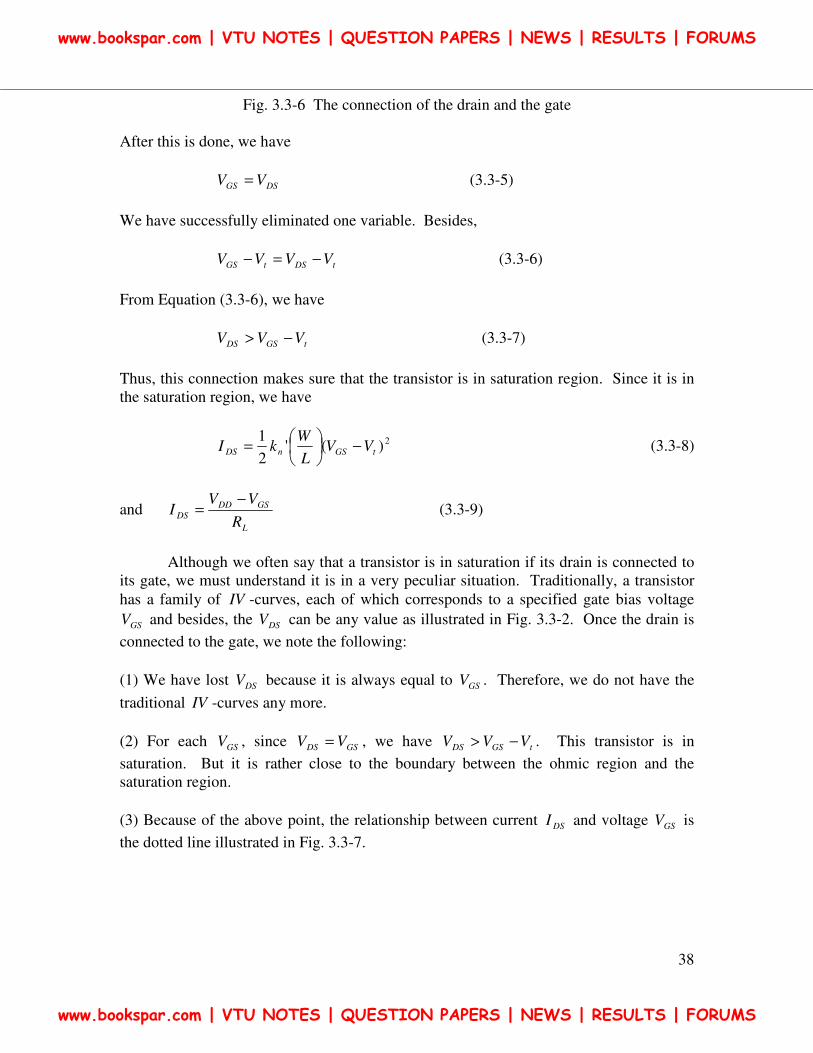
38
Fig. 3.3-6 The connection of the drain and the gate
After this is done, we have
DSGS VV = (3.3-5)
We have successfully eliminated one variable. Besides,
tDStGS VVVV −=− (3.3-6)
From Equation (3.3-6), we have
tGSDS VVV −> (3.3-7)
Thus, this connection makes sure that the transistor is in saturation region. Since it is in
the saturation region, we have
2)('2
1tGSnDS VV
L
WkI −
= (3.3-8)
and L
GSDD
DSR
VVI
−= (3.3-9)
Although we often say that a transistor is in saturation if its drain is connected to
its gate, we must understand it is in a very peculiar situation. Traditionally, a transistor
has a family of IV -curves, each of which corresponds to a specified gate bias voltage
GSV and besides, the DSV can be any value as illustrated in Fig. 3.3-2. Once the drain is
connected to the gate, we note the following:
(1) We have lost DSV because it is always equal to GSV . Therefore, we do not have the
traditional IV -curves any more.
(2) For each GSV , since GSDS VV = , we have tGSDS VVV −> . This transistor is in
saturation. But it is rather close to the boundary between the ohmic region and the
saturation region.
(3) Because of the above point, the relationship between current DSI and voltage GSV is
the dotted line illustrated in Fig. 3.3-7.
www.bookspar.com | VTU NOTES | QUESTION PAPERS | NEWS | RESULTS | FORUMS
www.bookspar.com | VTU NOTES | QUESTION PAPERS | NEWS | RESULTS | FORUMS
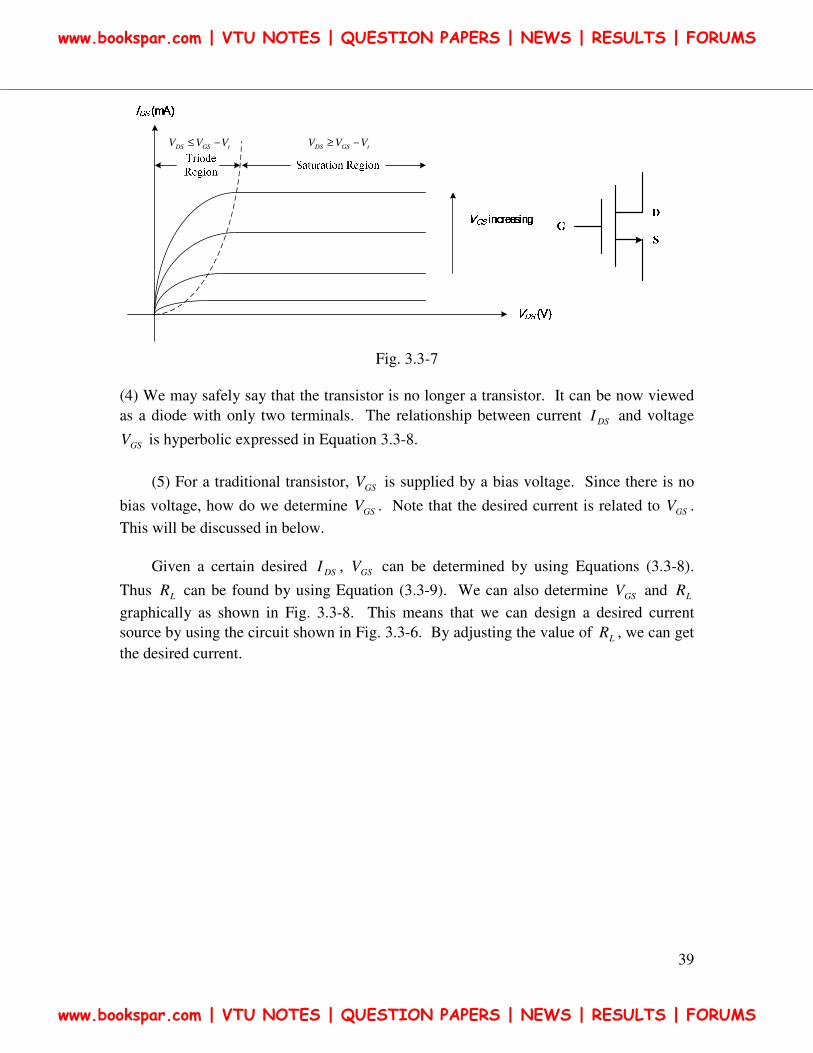
39
tGSDS VVV −≤ tGSDS VVV −≥
Fig. 3.3-7
(4) We may safely say that the transistor is no longer a transistor. It can be now viewed
as a diode with only two terminals. The relationship between current DSI and voltage
GSV is hyperbolic expressed in Equation 3.3-8.
(5) For a traditional transistor, GSV is supplied by a bias voltage. Since there is no
bias voltage, how do we determine GSV . Note that the desired current is related to GSV .
This will be discussed in below.
Given a certain desired DSI , GSV can be determined by using Equations (3.3-8).
Thus LR can be found by using Equation (3.3-9). We can also determine GSV and LR
graphically as shown in Fig. 3.3-8. This means that we can design a desired current
source by using the circuit shown in Fig. 3.3-6. By adjusting the value of LR , we can get
the desired current.
www.bookspar.com | VTU NOTES | QUESTION PAPERS | NEWS | RESULTS | FORUMS
www.bookspar.com | VTU NOTES | QUESTION PAPERS | NEWS | RESULTS | FORUMS
40
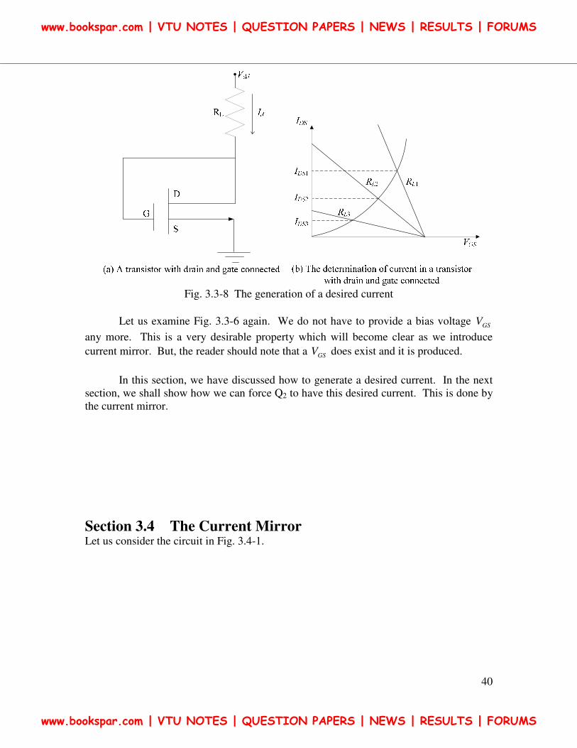
Fig. 3.3-8 The generation of a desired current
Let us examine Fig. 3.3-6 again. We do not have to provide a bias voltage GSV
any more. This is a very desirable property which will become clear as we introduce
current mirror. But, the reader should note that a GSV does exist and it is produced.
In this section, we have discussed how to generate a desired current. In the next
section, we shall show how we can force Q2 to have this desired current. This is done by
the current mirror.
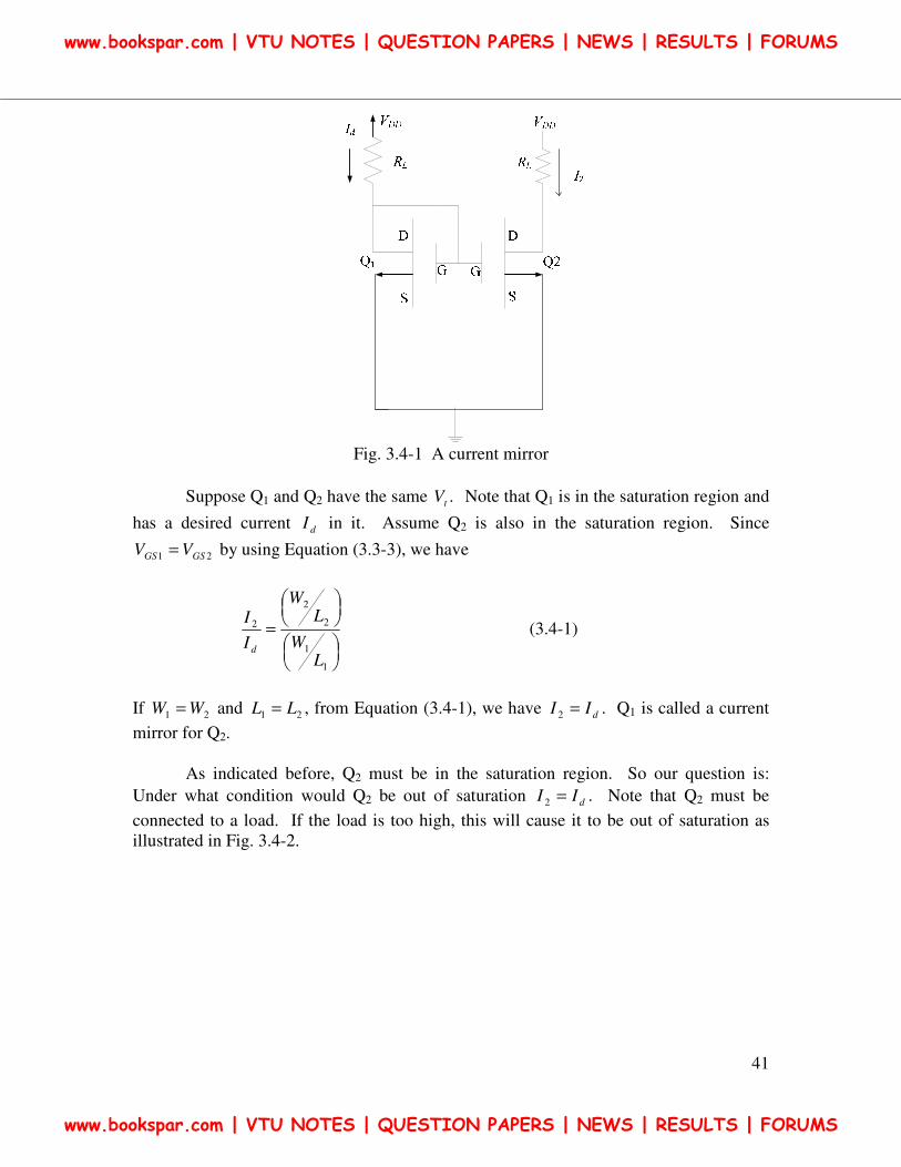
Section 3.4 The Current Mirror Let us consider the circuit in Fig. 3.4-1.
www.bookspar.com | VTU NOTES | QUESTION PAPERS | NEWS | RESULTS | FORUMS
www.bookspar.com | VTU NOTES | QUESTION PAPERS | NEWS | RESULTS | FORUMS
41
Fig. 3.4-1 A current mirror
Suppose Q1 and Q2 have the same .tV Note that Q1 is in the saturation region and
has a desired current dI in it. Assume Q2 is also in the saturation region. Since
21 GSGS VV = by using Equation (3.3-3), we have
=
1
1
2
2
2
LW
LW
I
I
d
(3.4-1)
If 21 WW = and 21 LL = , from Equation (3.4-1), we have dII =2 . Q1 is called a current
mirror for Q2.
As indicated before, Q2 must be in the saturation region. So our question is:
Under what condition would Q2 be out of saturation dII =2 . Note that Q2 must be
connected to a load. If the load is too high, this will cause it to be out of saturation as
illustrated in Fig. 3.4-2.
www.bookspar.com | VTU NOTES | QUESTION PAPERS | NEWS | RESULTS | FORUMS
www.bookspar.com | VTU NOTES | QUESTION PAPERS | NEWS | RESULTS | FORUMS
42
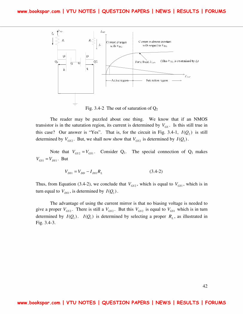
Fig. 3.4-2 The out of saturation of Q2
The reader may be puzzled about one thing. We know that if an NMOS
transistor is in the saturation region, its current is determined by GSV . Is this still true in
this case? Our answer is “Yes”. That is, for the circuit in Fig. 3.4-1, )( 2QI is still
determined by 2GSV . But, we shall now show that 2GSV is determined by )( 1QI .
Note that 12 GSGS VV = . Consider Q1. The special connection of Q1 makes
11 DSGS VV = . But
LDSDDDS RIVV 11 −= (3.4-2)
Thus, from Equation (3.4-2), we conclude that 2GSV , which is equal to 1GSV , which is in
turn equal to 1DSV , is determined by )( 1QI .
The advantage of using the current mirror is that no biasing voltage is needed to
give a proper 2GSV . There is still a 2GSV . But this 2GSV is equal to 1GSV which is in turn
determined by )( 1QI . )( 1QI is determined by selecting a proper LR , as illustrated in
Fig. 3.4-3.
www.bookspar.com | VTU NOTES | QUESTION PAPERS | NEWS | RESULTS | FORUMS
www.bookspar.com | VTU NOTES | QUESTION PAPERS | NEWS | RESULTS | FORUMS
43
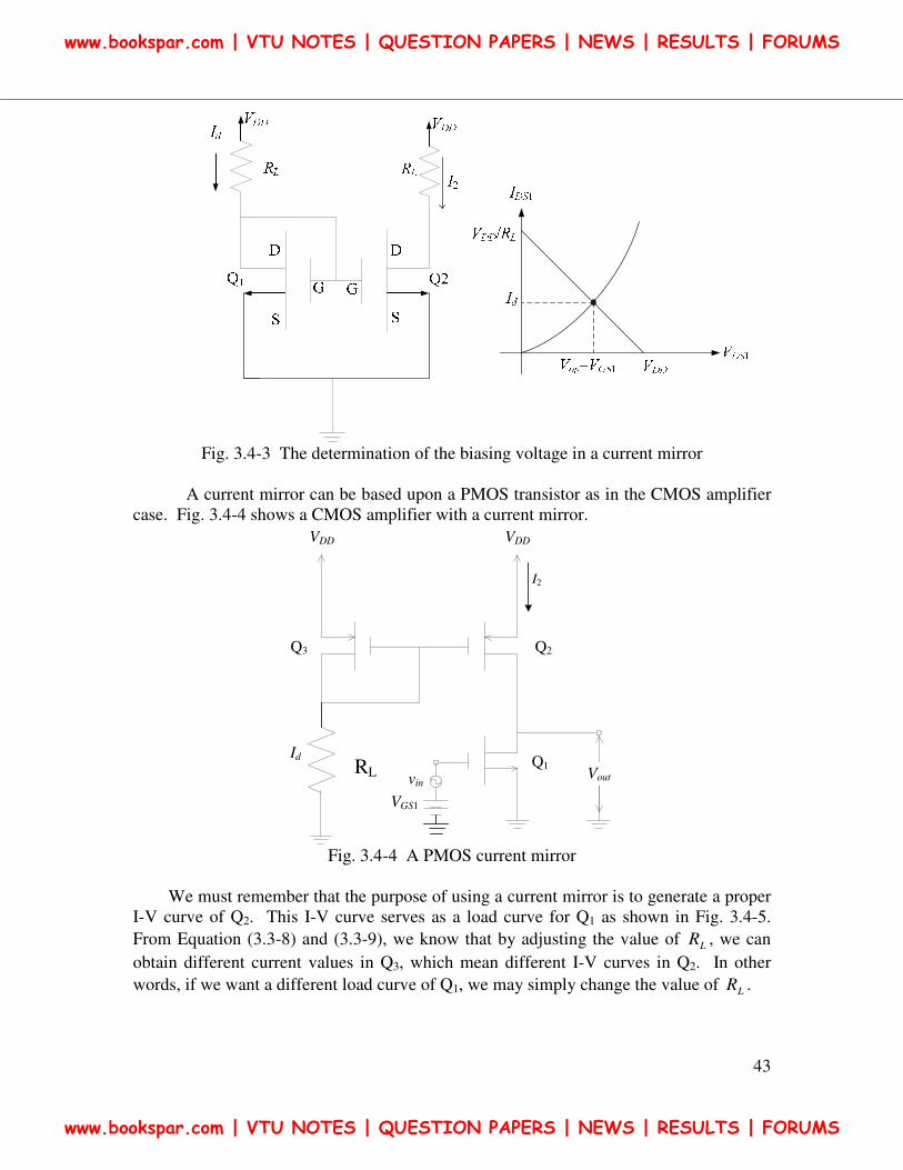
Fig. 3.4-3 The determination of the biasing voltage in a current mirror
A current mirror can be based upon a PMOS transistor as in the CMOS amplifier
case. Fig. 3.4-4 shows a CMOS amplifier with a current mirror.
Vout
VDD VDD
Q3 Q2
Q1Id
I2
AC
VGS1
vin
RL
Fig. 3.4-4 A PMOS current mirror
We must remember that the purpose of using a current mirror is to generate a proper
I-V curve of Q2. This I-V curve serves as a load curve for Q1 as shown in Fig. 3.4-5.
From Equation (3.3-8) and (3.3-9), we know that by adjusting the value of LR , we can
obtain different current values in Q3, which mean different I-V curves in Q2. In other
words, if we want a different load curve of Q1, we may simply change the value of LR .
www.bookspar.com | VTU NOTES | QUESTION PAPERS | NEWS | RESULTS | FORUMS
www.bookspar.com | VTU NOTES | QUESTION PAPERS | NEWS | RESULTS | FORUMS
44
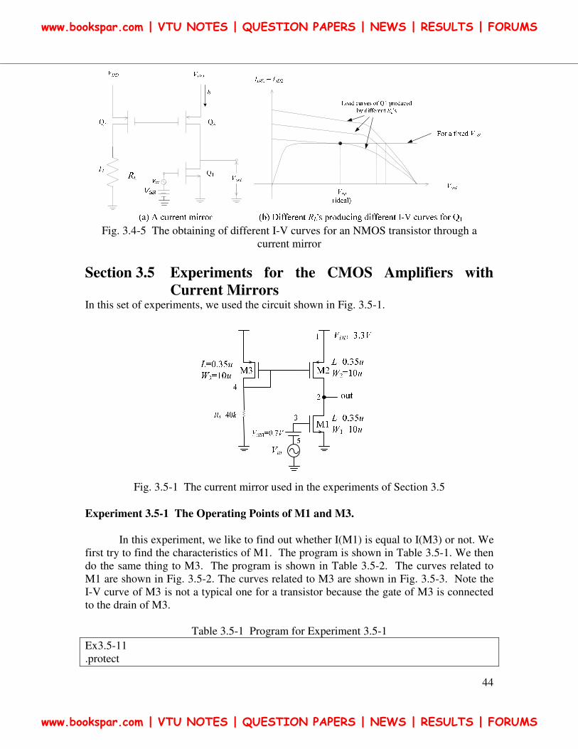
Fig. 3.4-5 The obtaining of different I-V curves for an NMOS transistor through a
current mirror
Section 3.5 Experiments for the CMOS Amplifiers with
Current Mirrors In this set of experiments, we used the circuit shown in Fig. 3.5-1.
Fig. 3.5-1 The current mirror used in the experiments of Section 3.5
Experiment 3.5-1 The Operating Points of M1 and M3.
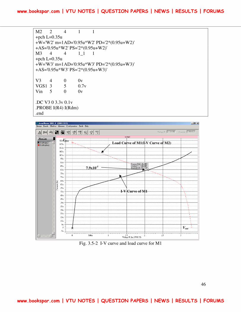
In this experiment, we like to find out whether I(M1) is equal to I(M3) or not. We
first try to find the characteristics of M1. The program is shown in Table 3.5-1. We then
do the same thing to M3. The program is shown in Table 3.5-2. The curves related to
M1 are shown in Fig. 3.5-2. The curves related to M3 are shown in Fig. 3.5-3. Note the
I-V curve of M3 is not a typical one for a transistor because the gate of M3 is connected
to the drain of M3.
Table 3.5-1 Program for Experiment 3.5-1
Ex3.5-11
.protect
www.bookspar.com | VTU NOTES | QUESTION PAPERS | NEWS | RESULTS | FORUMS
www.bookspar.com | VTU NOTES | QUESTION PAPERS | NEWS | RESULTS | FORUMS
45
.lib 'C:\model\tsmc\MIXED035\mm0355v.l' TT
.unprotect
.op
.options nomod post
VDD 1 0 3.3v
R4 4 0 30k
Rdm 1 1_1 0
.param W1=10u W2=10u W3=10u W4=10u
M1 2 3 0 0
+nch L=0.35u W='W1' m=1 AD='0.95u*W1'
+PD='2*(0.95u+W1)' AS='0.95u*W1' PS='2*(0.95u+W1)'
M2 2 4 1_1 1
+pch L=0.35u
+W='W2' m=1 AD='0.95u*W2' PD='2*(0.95u+W2)'
+AS='0.95u*W2' PS='2*(0.95u+W2)'
M3 4 4 1 1
+pch L=0.35u
+W='W3' m=1 AD='0.95u*W3' PD='2*(0.95u+W3)'
+AS='0.95u*W3' PS='2*(0.95u+W3)'
V2 2 0 0v
VGS1 3 5 0.7v
Vin 5 0 0v
.DC V2 0 3.3v 0.1v
.PROBE I(M1) I(Rdm)
.end
Table 3.5-2 Another program for Experiment 3.5-1
Ex3.5-12
.protect
.lib 'c:\mm0355v.l' TT
.unprotect
.op
.options nomod post
VDD 1 0 3.3v
R4 4 0 30k
Rdm 1 1_1 0
.param W1=10u W2=10u W3=10u W4=10u
M1 2 3 0 0
+nch L=0.35u W='W1' m=1 AD='0.95u*W1'
+PD='2*(0.95u+W1)' AS='0.95u*W1' PS='2*(0.95u+W1)'
www.bookspar.com | VTU NOTES | QUESTION PAPERS | NEWS | RESULTS | FORUMS
www.bookspar.com | VTU NOTES | QUESTION PAPERS | NEWS | RESULTS | FORUMS
46
M2 2 4 1 1
+pch L=0.35u
+W='W2' m=1 AD='0.95u*W2' PD='2*(0.95u+W2)'
+AS='0.95u*W2' PS='2*(0.95u+W2)'
M3 4 4 1_1 1
+pch L=0.35u
+W='W3' m=1 AD='0.95u*W3' PD='2*(0.95u+W3)'
+AS='0.95u*W3' PS='2*(0.95u+W3)'
V3 4 0 0v
VGS1 3 5 0.7v
Vin 5 0 0v
.DC V3 0 3.3v 0.1v
.PROBE I(R4) I(Rdm)
.end
Fig. 3.5-2 I-V curve and load curve for M1
Load Curve of M1(I-V Curve of M2)
I-V Curve of M1
Vout
IDS1
7.9x10⁻⁵
www.bookspar.com | VTU NOTES | QUESTION PAPERS | NEWS | RESULTS | FORUMS
www.bookspar.com | VTU NOTES | QUESTION PAPERS | NEWS | RESULTS | FORUMS
47
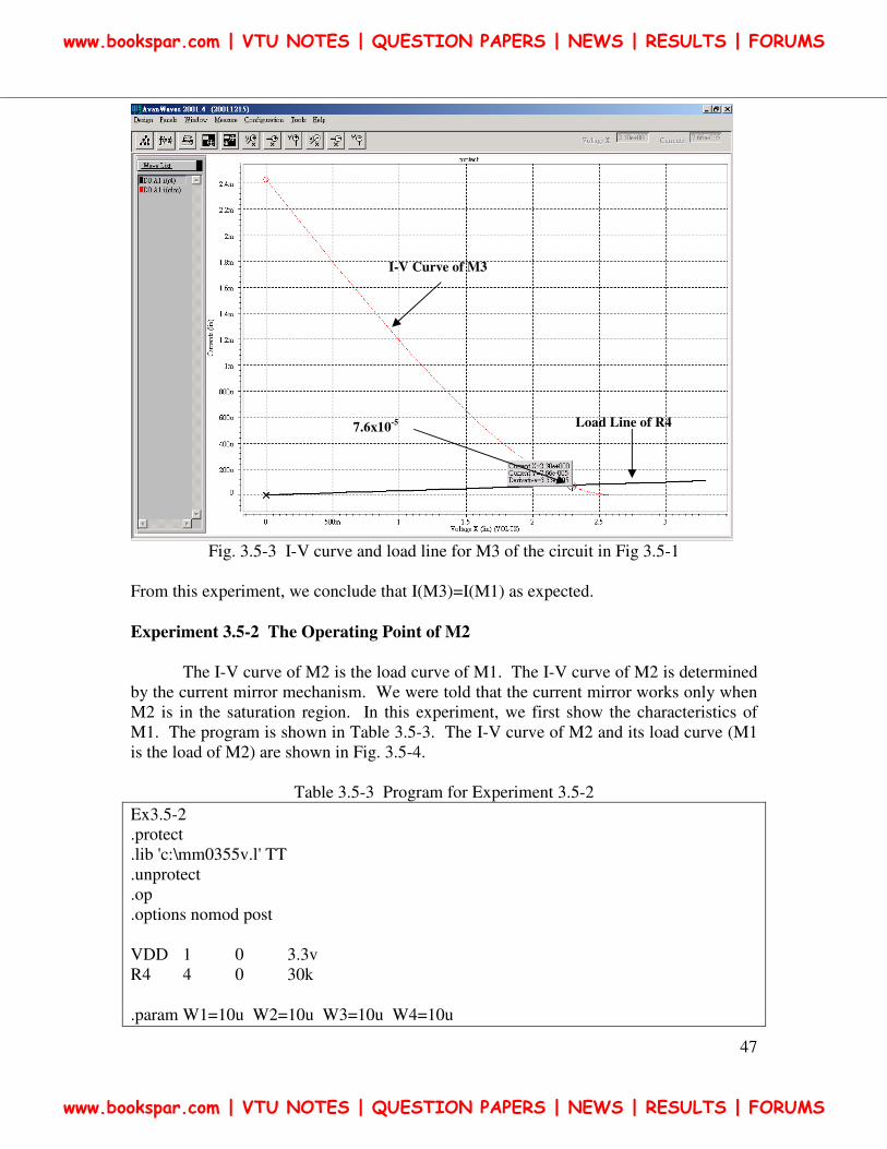
Fig. 3.5-3 I-V curve and load line for M3 of the circuit in Fig 3.5-1
From this experiment, we conclude that I(M3)=I(M1) as expected.
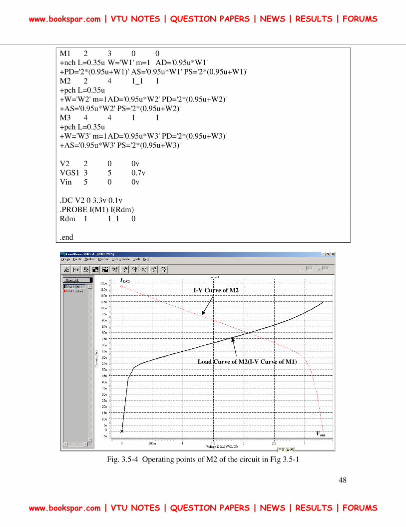
Experiment 3.5-2 The Operating Point of M2
The I-V curve of M2 is the load curve of M1. The I-V curve of M2 is determined
by the current mirror mechanism. We were told that the current mirror works only when
M2 is in the saturation region. In this experiment, we first show the characteristics of
M1. The program is shown in Table 3.5-3. The I-V curve of M2 and its load curve (M1
is the load of M2) are shown in Fig. 3.5-4.
Table 3.5-3 Program for Experiment 3.5-2
Ex3.5-2
.protect
.lib 'c:\mm0355v.l' TT
.unprotect
.op
.options nomod post
VDD 1 0 3.3v
R4 4 0 30k
.param W1=10u W2=10u W3=10u W4=10u
Load Line of R4
I-V Curve of M3
7.6x10⁻⁵
www.bookspar.com | VTU NOTES | QUESTION PAPERS | NEWS | RESULTS | FORUMS
www.bookspar.com | VTU NOTES | QUESTION PAPERS | NEWS | RESULTS | FORUMS
48
M1 2 3 0 0
+nch L=0.35u W='W1' m=1 AD='0.95u*W1'
+PD='2*(0.95u+W1)' AS='0.95u*W1' PS='2*(0.95u+W1)'
M2 2 4 1_1 1
+pch L=0.35u
+W='W2' m=1 AD='0.95u*W2' PD='2*(0.95u+W2)'
+AS='0.95u*W2' PS='2*(0.95u+W2)'
M3 4 4 1 1
+pch L=0.35u
+W='W3' m=1 AD='0.95u*W3' PD='2*(0.95u+W3)'
+AS='0.95u*W3' PS='2*(0.95u+W3)'
V2 2 0 0v
VGS1 3 5 0.7v
Vin 5 0 0v
.DC V2 0 3.3v 0.1v
.PROBE I(M1) I(Rdm)
Rdm 1 1_1 0
.end
Fig. 3.5-4 Operating points of M2 of the circuit in Fig 3.5-1
Vout
IDS2
I-V Curve of M2
Load Curve of M2(I-V Curve of M1)
www.bookspar.com | VTU NOTES | QUESTION PAPERS | NEWS | RESULTS | FORUMS
www.bookspar.com | VTU NOTES | QUESTION PAPERS | NEWS | RESULTS | FORUMS
49
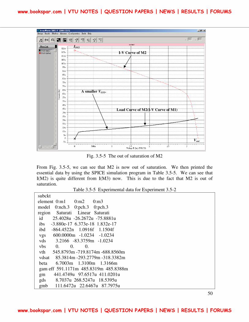
As shown in Fig. 3.5-4, M2 is in the saturation region.
To drive M2 out of the saturation region, we lowered 1GSV from 0.7V to 0.6V.
The program is shown in Table 3.5-4 and the curves are shown in Fig. 3.5-5.
Table 3.5-4 The program to drive M2 out of saturation
Ex3.5-2b
.protect
.lib 'c:\mm0355v.l' TT
.unprotect
.op
.options nomod post
VDD 1 0 3.3v
R4 4 0 30k
.param W1=10u W2=10u W3=10u W4=10u
M1 2 3 0 0
+nch L=0.35u W='W1' m=1 AD='0.95u*W1'
+PD='2*(0.95u+W1)' AS='0.95u*W1' PS='2*(0.95u+W1)'
M2 2 4 1_1 1
+pch L=0.35u
+W='W2' m=1 AD='0.95u*W2' PD='2*(0.95u+W2)'
+AS='0.95u*W2' PS='2*(0.95u+W2)'
M3 4 4 1 1
+pch L=0.35u
+W='W3' m=1 AD='0.95u*W3' PD='2*(0.95u+W3)'
+AS='0.95u*W3' PS='2*(0.95u+W3)'
V2 2 0 0v
VGS1 3 5 0.6v
Vin 5 0 0v
.DC V2 0 3.3v 0.1v
.PROBE I(M1) I(Rdm)
Rdm 1 1_1 0
.end
www.bookspar.com | VTU NOTES | QUESTION PAPERS | NEWS | RESULTS | FORUMS
www.bookspar.com | VTU NOTES | QUESTION PAPERS | NEWS | RESULTS | FORUMS
50
Fig. 3.5-5 The out of saturation of M2
From Fig. 3.5-5, we can see that M2 is now out of saturation. We then printed the
essential data by using the SPICE simulation program in Table 3.5-5. We can see that
I(M2) is quite different from I(M3) now. This is due to the fact that M2 is out of
saturation.
Table 3.5-5 Experimental data for Experiment 3.5-2
subckt
element 0:m1 0:m2 0:m3
model 0:nch.3 0:pch.3 0:pch.3
region Saturati Linear Saturati
id 25.4028u -26.2672u -75.8881u
ibs -3.880e-17 6.373e-18 1.832e-17
ibd -864.4522n 1.0916f 1.1504f
vgs 600.0000m -1.0234 -1.0234
vds 3.2166 -83.3759m -1.0234
vbs 0. 0. 0.
vth 545.8793m -719.8174m -688.8560m
vdsat 85.3814m -293.2779m -318.3382m
beta 6.7003m 1.3100m 1.3166m
gam eff 591.1171m 485.8319m 485.8388m
gm 441.4749u 97.6517u 411.0201u
gds 8.7037u 268.5247u 18.5395u
gmb 111.6472u 22.6467u 87.7975u
Vout
IDS2
I-V Curve of M2
Load Curve of M2(I-V Curve of M1)
A smaller VGS1.
www.bookspar.com | VTU NOTES | QUESTION PAPERS | NEWS | RESULTS | FORUMS
www.bookspar.com | VTU NOTES | QUESTION PAPERS | NEWS | RESULTS | FORUMS
51
cdtot 11.3338f 28.6456f 14.4251f
cgtot 10.2012f 16.2693f 12.7341f
cstot 21.1660f 31.1152f 30.5144f
cbtot 27.1028f 38.9009f 33.8541f
cgs 5.6263f 8.8368f 9.9096f
cgd 2.0774f 7.2706f 1.8392f
Experiment 3.5-3 The DC Input-Output Relationship of M1.
In this experiment, weplotted 1DSV versus 1GSV . The program is in Table 3.5-6
and the DC input-output relationship is shown in Fig. 3.5-6.
Table 3.5-6 Program of Experiment 3.5-3
.protect
.lib 'c:\mm0355v.l' TT
.unprotect
.op
.options nomod post
VDD 1 0 3.3v
R4 4 0 30k
.param W1=10u W2=10u W3=10u W4=10u
M1 2 3 0 0
+nch L=0.35u W='W1' m=1 AD='0.95u*W1'
+PD='2*(0.95u+W1)' AS='0.95u*W1' PS='2*(0.95u+W1)'
M2 2 4 1 1
+pch L=0.35u
+W='W2' m=1 AD='0.95u*W2' PD='2*(0.95u+W2)'
+AS='0.95u*W2' PS='2*(0.95u+W2)'
M3 4 4 1 1
+pch L=0.35u
+W='W3' m=1 AD='0.95u*W3' PD='2*(0.95u+W3)'
+AS='0.95u*W3' PS='2*(0.95u+W3)'
VGS1 3 0 0v
.DC VGS1 0 3.3v 0.1v
.PROBE I(M1)
.end
www.bookspar.com | VTU NOTES | QUESTION PAPERS | NEWS | RESULTS | FORUMS
www.bookspar.com | VTU NOTES | QUESTION PAPERS | NEWS | RESULTS | FORUMS
52
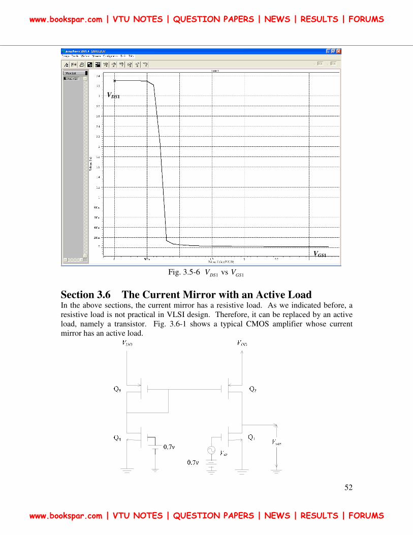
Fig. 3.5-6 1DSV vs 1GSV
Section 3.6 The Current Mirror with an Active Load In the above sections, the current mirror has a resistive load. As we indicated before, a
resistive load is not practical in VLSI design. Therefore, it can be replaced by an active
load, namely a transistor. Fig. 3.6-1 shows a typical CMOS amplifier whose current
mirror has an active load.
VGS1
VDS1
www.bookspar.com | VTU NOTES | QUESTION PAPERS | NEWS | RESULTS | FORUMS
www.bookspar.com | VTU NOTES | QUESTION PAPERS | NEWS | RESULTS | FORUMS
53
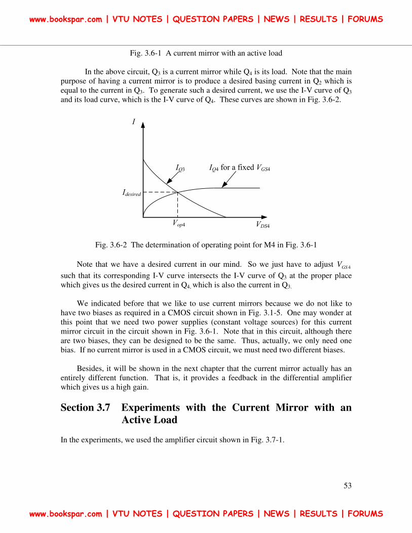
Fig. 3.6-1 A current mirror with an active load
In the above circuit, Q3 is a current mirror while Q4 is its load. Note that the main
purpose of having a current mirror is to produce a desired basing current in Q2 which is
equal to the current in Q3. To generate such a desired current, we use the I-V curve of Q3
and its load curve, which is the I-V curve of Q4. These curves are shown in Fig. 3.6-2.
VDS4
I
Vop4
IQ3 IQ4 for a fixed VGS4
Idesired
Fig. 3.6-2 The determination of operating point for M4 in Fig. 3.6-1
Note that we have a desired current in our mind. So we just have to adjust 4GSV
such that its corresponding I-V curve intersects the I-V curve of Q3 at the proper place
which gives us the desired current in Q4, which is also the current in Q3.
We indicated before that we like to use current mirrors because we do not like to
have two biases as required in a CMOS circuit shown in Fig. 3.1-5. One may wonder at
this point that we need two power supplies (constant voltage sources) for this current
mirror circuit in the circuit shown in Fig. 3.6-1. Note that in this circuit, although there
are two biases, they can be designed to be the same. Thus, actually, we only need one
bias. If no current mirror is used in a CMOS circuit, we must need two different biases.
Besides, it will be shown in the next chapter that the current mirror actually has an
entirely different function. That is, it provides a feedback in the differential amplifier
which gives us a high gain.
Section 3.7 Experiments with the Current Mirror with an
Active Load
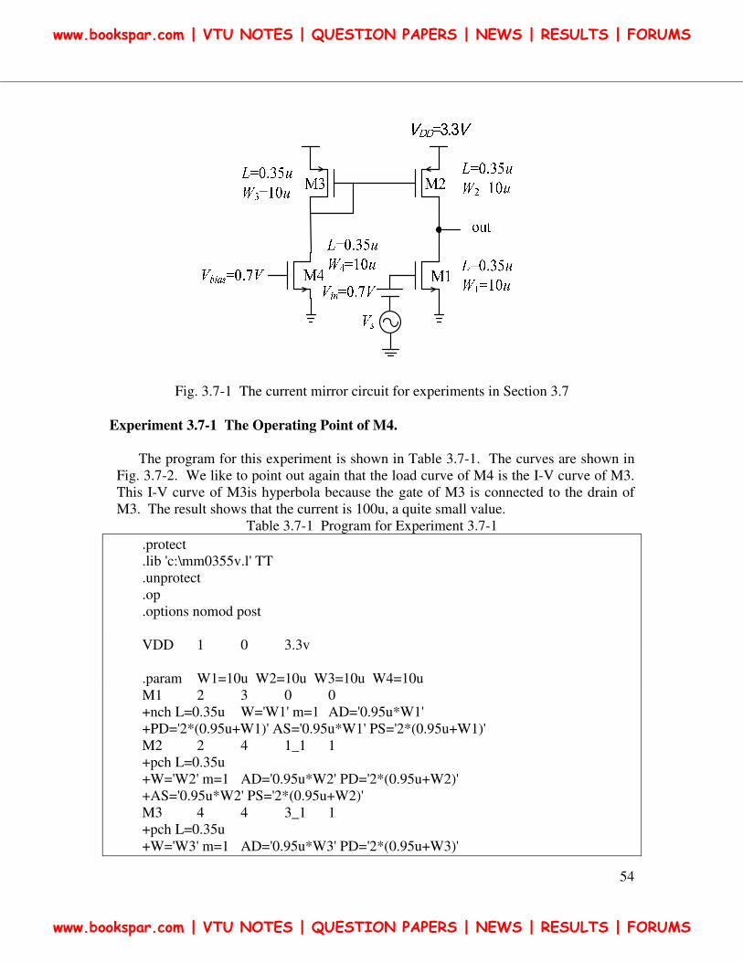
In the experiments, we used the amplifier circuit shown in Fig. 3.7-1.
www.bookspar.com | VTU NOTES | QUESTION PAPERS | NEWS | RESULTS | FORUMS
www.bookspar.com | VTU NOTES | QUESTION PAPERS | NEWS | RESULTS | FORUMS
54
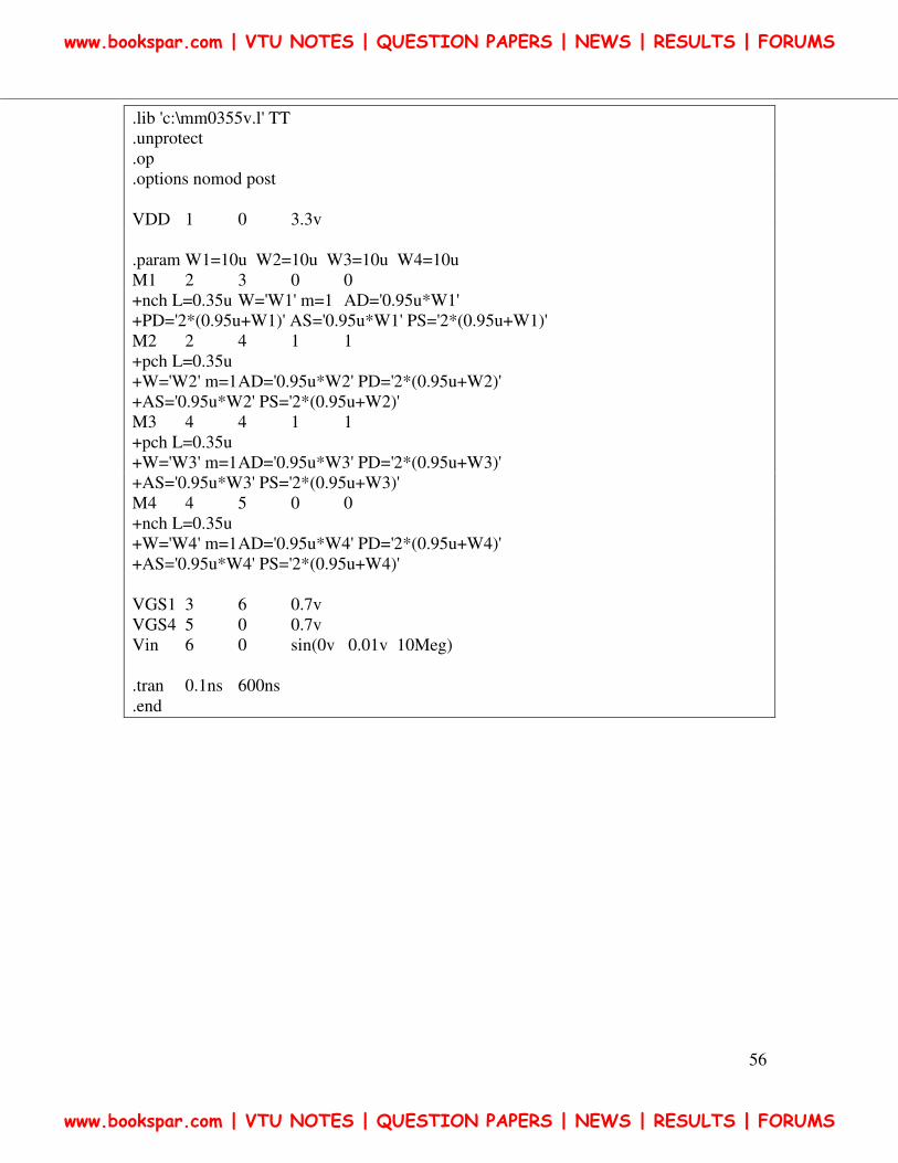
Fig. 3.7-1 The current mirror circuit for experiments in Section 3.7
Experiment 3.7-1 The Operating Point of M4.
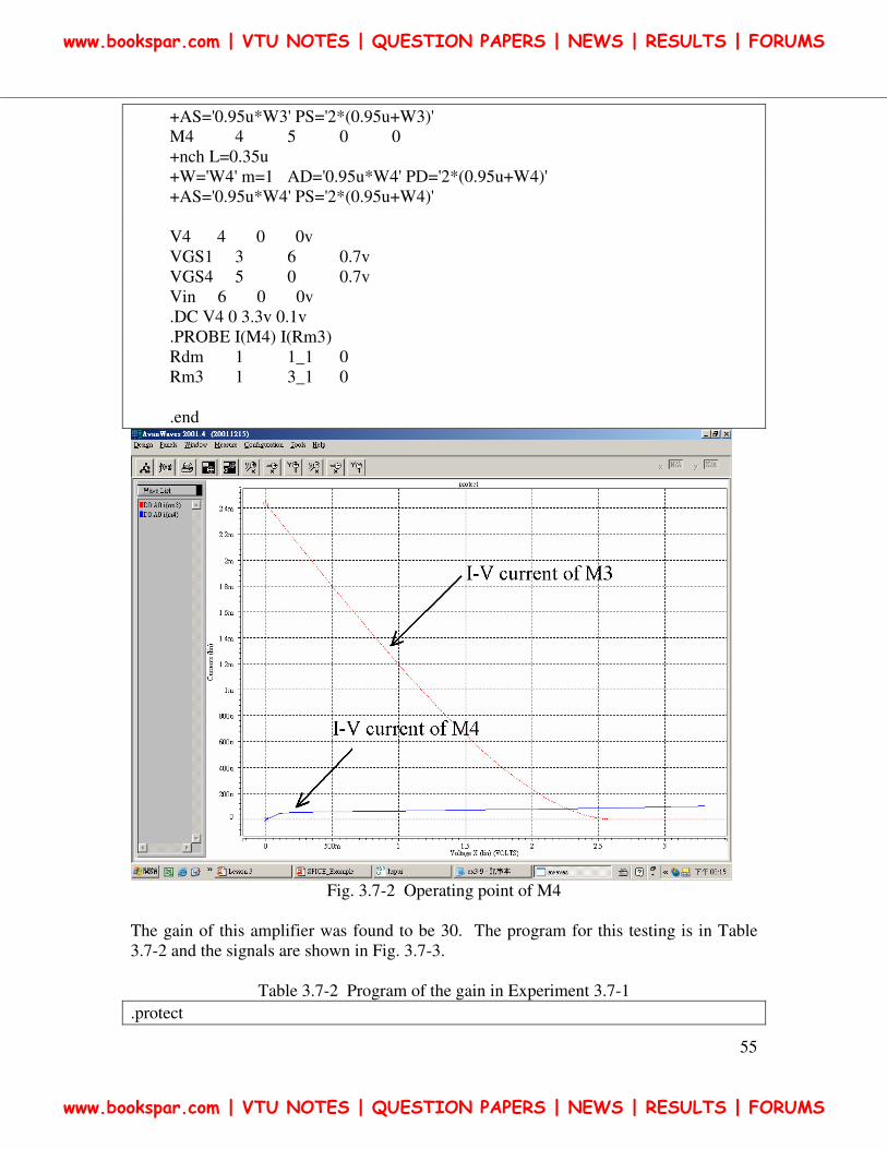
The program for this experiment is shown in Table 3.7-1. The curves are shown in
Fig. 3.7-2. We like to point out again that the load curve of M4 is the I-V curve of M3.
This I-V curve of M3is hyperbola because the gate of M3 is connected to the drain of
M3. The result shows that the current is 100u, a quite small value.
Table 3.7-1 Program for Experiment 3.7-1
.protect
.lib 'c:\mm0355v.l' TT
.unprotect
.op
.options nomod post
VDD 1 0 3.3v
.param W1=10u W2=10u W3=10u W4=10u
M1 2 3 0 0
+nch L=0.35u W='W1' m=1 AD='0.95u*W1'
+PD='2*(0.95u+W1)' AS='0.95u*W1' PS='2*(0.95u+W1)'
M2 2 4 1_1 1
+pch L=0.35u
+W='W2' m=1 AD='0.95u*W2' PD='2*(0.95u+W2)'
+AS='0.95u*W2' PS='2*(0.95u+W2)'
M3 4 4 3_1 1
+pch L=0.35u
+W='W3' m=1 AD='0.95u*W3' PD='2*(0.95u+W3)'
www.bookspar.com | VTU NOTES | QUESTION PAPERS | NEWS | RESULTS | FORUMS
www.bookspar.com | VTU NOTES | QUESTION PAPERS | NEWS | RESULTS | FORUMS
55
+AS='0.95u*W3' PS='2*(0.95u+W3)'
M4 4 5 0 0
+nch L=0.35u
+W='W4' m=1 AD='0.95u*W4' PD='2*(0.95u+W4)'
+AS='0.95u*W4' PS='2*(0.95u+W4)'
V4 4 0 0v
VGS1 3 6 0.7v
VGS4 5 0 0.7v
Vin 6 0 0v
.DC V4 0 3.3v 0.1v
.PROBE I(M4) I(Rm3)
Rdm 1 1_1 0
Rm3 1 3_1 0
.end
Fig. 3.7-2 Operating point of M4
The gain of this amplifier was found to be 30. The program for this testing is in Table
3.7-2 and the signals are shown in Fig. 3.7-3.
Table 3.7-2 Program of the gain in Experiment 3.7-1
.protect
www.bookspar.com | VTU NOTES | QUESTION PAPERS | NEWS | RESULTS | FORUMS
www.bookspar.com | VTU NOTES | QUESTION PAPERS | NEWS | RESULTS | FORUMS
56
.lib 'c:\mm0355v.l' TT
.unprotect
.op
.options nomod post
VDD 1 0 3.3v
.param W1=10u W2=10u W3=10u W4=10u
M1 2 3 0 0
+nch L=0.35u W='W1' m=1 AD='0.95u*W1'
+PD='2*(0.95u+W1)' AS='0.95u*W1' PS='2*(0.95u+W1)'
M2 2 4 1 1
+pch L=0.35u
+W='W2' m=1 AD='0.95u*W2' PD='2*(0.95u+W2)'
+AS='0.95u*W2' PS='2*(0.95u+W2)'
M3 4 4 1 1
+pch L=0.35u
+W='W3' m=1 AD='0.95u*W3' PD='2*(0.95u+W3)'
+AS='0.95u*W3' PS='2*(0.95u+W3)'
M4 4 5 0 0
+nch L=0.35u
+W='W4' m=1 AD='0.95u*W4' PD='2*(0.95u+W4)'
+AS='0.95u*W4' PS='2*(0.95u+W4)'
VGS1 3 6 0.7v
VGS4 5 0 0.7v
Vin 6 0 sin(0v 0.01v 10Meg)
.tran 0.1ns 600ns
.end
www.bookspar.com | VTU NOTES | QUESTION PAPERS | NEWS | RESULTS | FORUMS
www.bookspar.com | VTU NOTES | QUESTION PAPERS | NEWS | RESULTS | FORUMS
57
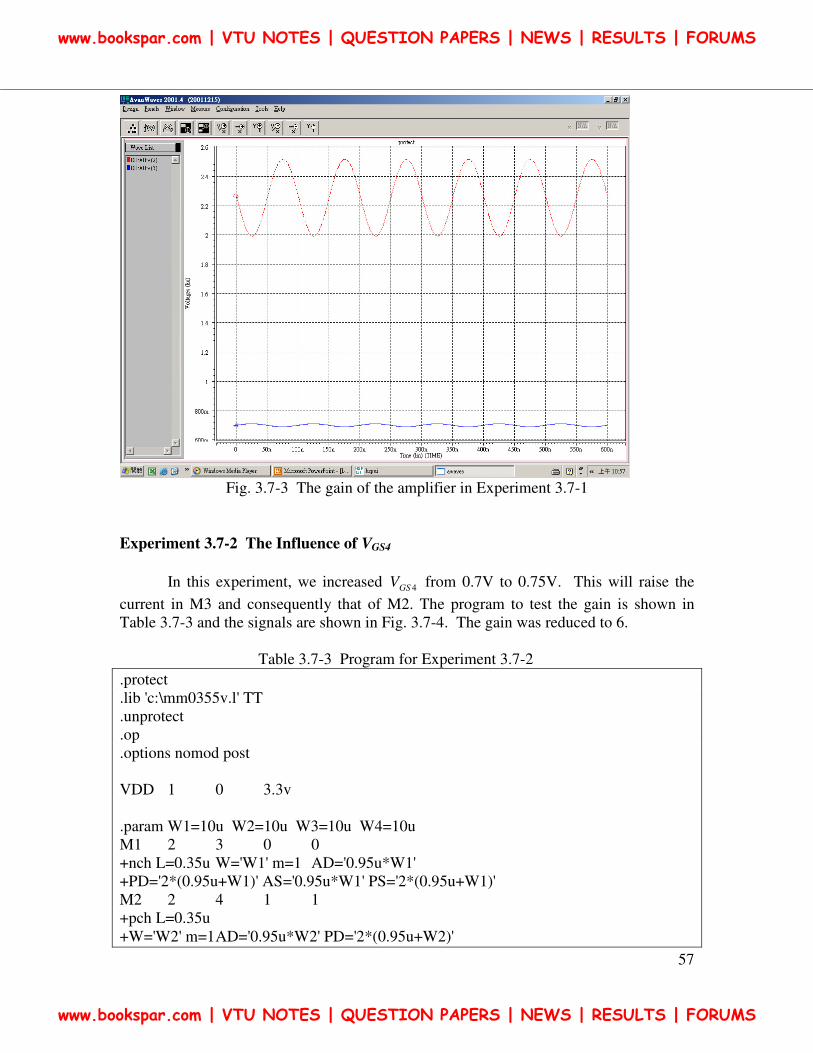
Fig. 3.7-3 The gain of the amplifier in Experiment 3.7-1
Experiment 3.7-2 The Influence of VGS4
In this experiment, we increased 4GSV from 0.7V to 0.75V. This will raise the
current in M3 and consequently that of M2. The program to test the gain is shown in
Table 3.7-3 and the signals are shown in Fig. 3.7-4. The gain was reduced to 6.
Table 3.7-3 Program for Experiment 3.7-2
.protect
.lib 'c:\mm0355v.l' TT
.unprotect
.op
.options nomod post
VDD 1 0 3.3v
.param W1=10u W2=10u W3=10u W4=10u
M1 2 3 0 0
+nch L=0.35u W='W1' m=1 AD='0.95u*W1'
+PD='2*(0.95u+W1)' AS='0.95u*W1' PS='2*(0.95u+W1)'
M2 2 4 1 1
+pch L=0.35u
+W='W2' m=1 AD='0.95u*W2' PD='2*(0.95u+W2)'
www.bookspar.com | VTU NOTES | QUESTION PAPERS | NEWS | RESULTS | FORUMS
www.bookspar.com | VTU NOTES | QUESTION PAPERS | NEWS | RESULTS | FORUMS
58
+AS='0.95u*W2' PS='2*(0.95u+W2)'
M3 4 4 1 1
+pch L=0.35u
+W='W3' m=1 AD='0.95u*W3' PD='2*(0.95u+W3)'
+AS='0.95u*W3' PS='2*(0.95u+W3)'
M4 4 5 0 0
+nch L=0.35u
+W='W4' m=1 AD='0.95u*W4' PD='2*(0.95u+W4)'
+AS='0.95u*W4' PS='2*(0.95u+W4)'
VGS1 3 6 0.7v
VGS4 5 0 0.75v
Vin 6 0 sin(0v 0.01v 10Meg)
.tran 0.1ns 600ns
.end
Fig. 3.7-4 The gain in Experiment 3.7-2
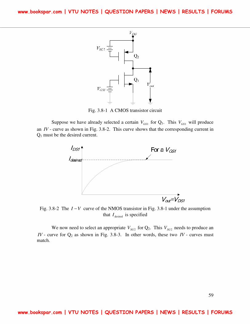
Section 3.8 A Summary of the Current Mirror Technology
To make the idea of the current mirror clear, let us make a summary of it as
follows. Consider the CMOS transistor circuit as shown in Fig. 3.8-1.
www.bookspar.com | VTU NOTES | QUESTION PAPERS | NEWS | RESULTS | FORUMS
www.bookspar.com | VTU NOTES | QUESTION PAPERS | NEWS | RESULTS | FORUMS
59
Fig. 3.8-1 A CMOS transistor circuit
Suppose we have already selected a certain 1GSV for Q1. This 1GSV will produce
an IV - curve as shown in Fig. 3.8-2. This curve shows that the corresponding current in
Q1 must be the desired current.
Fig. 3.8-2 The VI − curve of the NMOS transistor in Fig. 3.8-1 under the assumption
that desiredI is specified
We now need to select an appropriate 2SGV for Q2. This 2SGV needs to produce an
IV - curve for Q2 as shown in Fig. 3.8-3. In other words, these two IV - curves must
match.
www.bookspar.com | VTU NOTES | QUESTION PAPERS | NEWS | RESULTS | FORUMS
www.bookspar.com | VTU NOTES | QUESTION PAPERS | NEWS | RESULTS | FORUMS
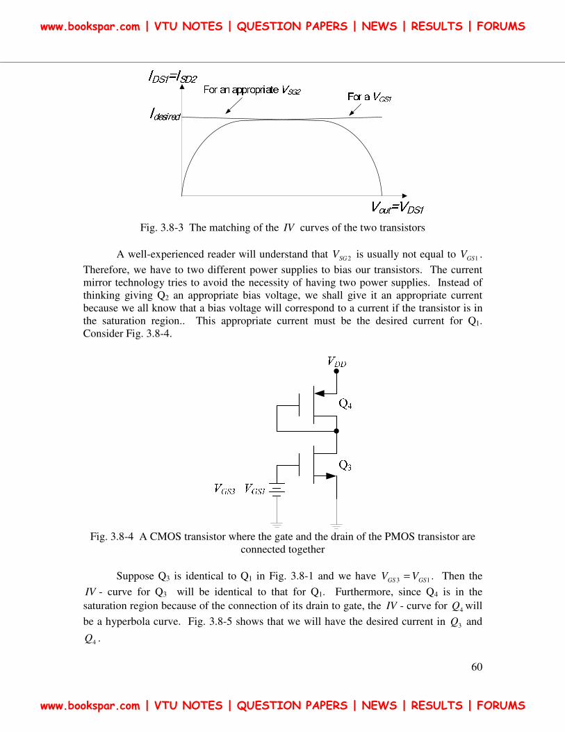
60
Fig. 3.8-3 The matching of the IV curves of the two transistors
A well-experienced reader will understand that 2SGV is usually not equal to 1GSV .
Therefore, we have to two different power supplies to bias our transistors. The current
mirror technology tries to avoid the necessity of having two power supplies. Instead of
thinking giving Q2 an appropriate bias voltage, we shall give it an appropriate current
because we all know that a bias voltage will correspond to a current if the transistor is in
the saturation region.. This appropriate current must be the desired current for Q1.
Consider Fig. 3.8-4.
Fig. 3.8-4 A CMOS transistor where the gate and the drain of the PMOS transistor are
connected together
Suppose Q3 is identical to Q1 in Fig. 3.8-1 and we have 13 GSGS VV = . Then the
IV - curve for Q3 will be identical to that for Q1. Furthermore, since Q4 is in the
saturation region because of the connection of its drain to gate, the IV - curve for 4Q will
be a hyperbola curve. Fig. 3.8-5 shows that we will have the desired current in 3Q and
4Q .
www.bookspar.com | VTU NOTES | QUESTION PAPERS | NEWS | RESULTS | FORUMS
www.bookspar.com | VTU NOTES | QUESTION PAPERS | NEWS | RESULTS | FORUMS
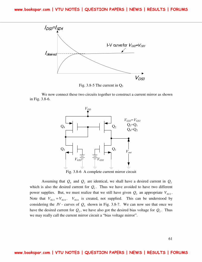
61
Fig. 3.8-5 The current in Q3
We now connect these two circuits together to construct a current mirror as shown
in Fig. 3.8-6.
Q4
Q3
VDD
Q2
Q1Vout
VGS1VGS3
VGS3=VGS1Q3=Q1Q4=Q2
Fig. 3.8-6 A complete current mirror circuit
Assuming that 4Q and 2Q are identical, we shall have a desired current in 2Q
which is also the desired current for 1Q . Thus we have avoided to have two different
power supplies. But, we must realize that we still have given 2Q an appropriate 2SGV .
Note that 42 SGSG VV = . 4SGV is created, not supplied. This can be understood by
considering the IV - curves of 4Q shown in Fig. 3.8-7. We can now see that once we
have the desired current for 2Q , we have also got the desired bias voltage for 2Q . Thus
we may really call the current mirror circuit a “bias voltage mirror”.
www.bookspar.com | VTU NOTES | QUESTION PAPERS | NEWS | RESULTS | FORUMS
www.bookspar.com | VTU NOTES | QUESTION PAPERS | NEWS | RESULTS | FORUMS
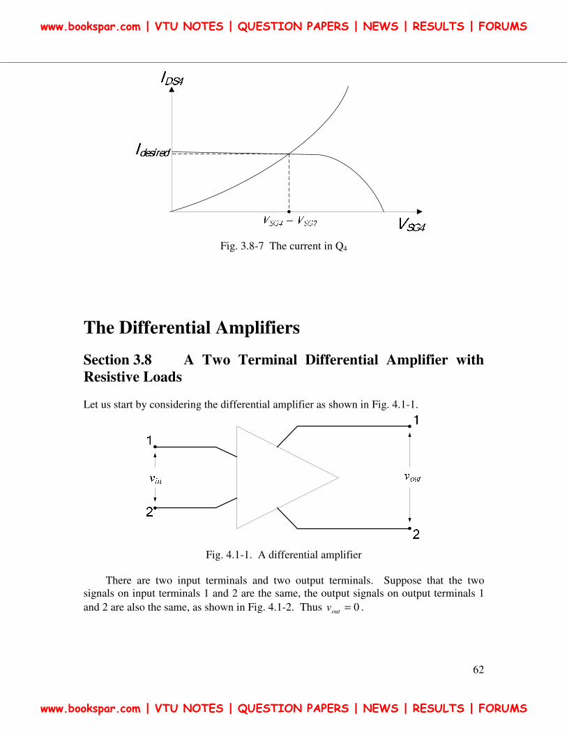
62
Fig. 3.8-7 The current in Q4
The Differential Amplifiers
Section 3.8 A Two Terminal Differential Amplifier with
Resistive Loads
Let us start by considering the differential amplifier as shown in Fig. 4.1-1.
Fig. 4.1-1. A differential amplifier
There are two input terminals and two output terminals. Suppose that the two
signals on input terminals 1 and 2 are the same, the output signals on output terminals 1
and 2 are also the same, as shown in Fig. 4.1-2. Thus 0=outv .
www.bookspar.com | VTU NOTES | QUESTION PAPERS | NEWS | RESULTS | FORUMS
www.bookspar.com | VTU NOTES | QUESTION PAPERS | NEWS | RESULTS | FORUMS
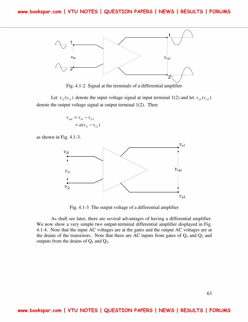
63
Fig. 4.1-2 Signal at the terminals of a differential amplifier
Let )( 21 ii vv denote the input voltage signal at input terminal 1(2) and let )( 21 oo vv
denote the output voltage signal at output terminal 1(2). Then
)( 21
21
ii
ooout
vva
vvv
−=
−=
as shown in Fig. 4.1-3.
Fig. 4.1-3 The output voltage of a differential amplifier
As shall see later, there are several advantages of having a differential amplifier.
We now show a very simple two output-terminal differential amplifier displayed in Fig.
4.1-4. Note that the input AC voltages are at the gates and the output AC voltages are at
the drains of the transistors. Note that there are AC inputs from gates of Q1 and Q2 and
outputs from the drains of Q1 and Q2.
www.bookspar.com | VTU NOTES | QUESTION PAPERS | NEWS | RESULTS | FORUMS
www.bookspar.com | VTU NOTES | QUESTION PAPERS | NEWS | RESULTS | FORUMS
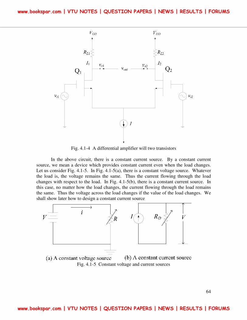
64
Fig. 4.1-4 A differential amplifier will two transistors
In the above circuit, there is a constant current source. By a constant current
source, we mean a device which provides constant current even when the load changes.
Let us consider Fig. 4.1-5. In Fig. 4.1-5(a), there is a constant voltage source. Whatever
the load is, the voltage remains the same. Thus the current flowing through the load
changes with respect to the load. In Fig. 4.1-5(b), there is a constant current source. In
this case, no matter how the load changes, the current flowing through the load remains
the same. Thus the voltage across the load changes if the value of the load changes. We
shall show later how to design a constant current source
Fig. 4.1-5 Constant voltage and current sources
www.bookspar.com | VTU NOTES | QUESTION PAPERS | NEWS | RESULTS | FORUMS
www.bookspar.com | VTU NOTES | QUESTION PAPERS | NEWS | RESULTS | FORUMS
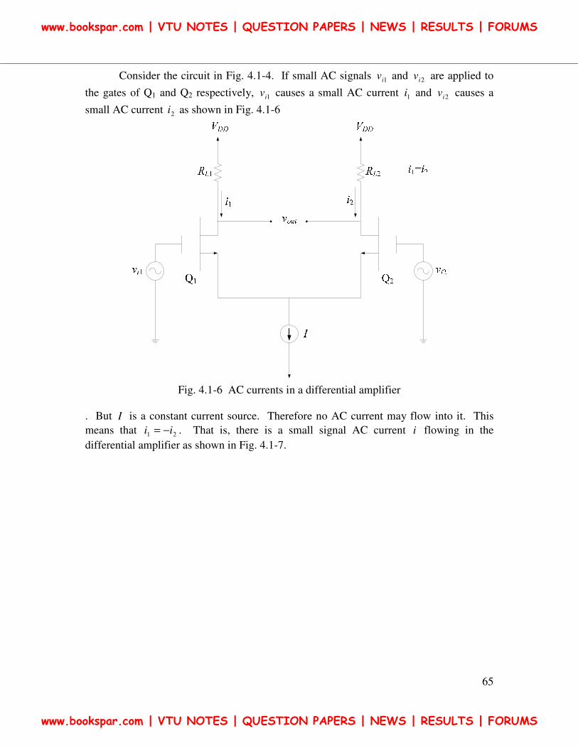
65
Consider the circuit in Fig. 4.1-4. If small AC signals 1iv and 2iv are applied to
the gates of Q1 and Q2 respectively, 1iv causes a small AC current 1i and 2iv causes a
small AC current 2i as shown in Fig. 4.1-6
Fig. 4.1-6 AC currents in a differential amplifier
. But I is a constant current source. Therefore no AC current may flow into it. This
means that 21 ii −= . That is, there is a small signal AC current i flowing in the
differential amplifier as shown in Fig. 4.1-7.
www.bookspar.com | VTU NOTES | QUESTION PAPERS | NEWS | RESULTS | FORUMS
www.bookspar.com | VTU NOTES | QUESTION PAPERS | NEWS | RESULTS | FORUMS
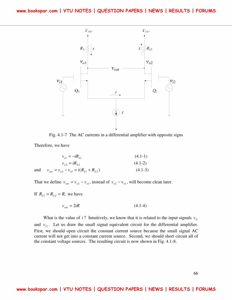
66
Fig. 4.1-7 The AC currents in a differential amplifier with opposite signs
Therefore, we have
11 Lo iRv −= (4.1-1)
22 Lo iRv = (4.1-2)
and )( 2112 LLooout RRivvv +=−= (4.1-3)
That we define 12 ooout vvv −= , instead of 12 oo vv − , will become clean later.
If ,21 RRR LL == we have
iRvout 2= (4.1-4)
What is the value of i ? Intuitively, we know that it is related to the input signals 1iv
and 2iv . Let us draw the small signal equivalent circuit for the differential amplifier.
First, we should open circuit the constant current source because the small signal AC
current will not get into a constant current source. Second, we should short circuit all of
the constant voltage sources. The resulting circuit is now shown in Fig. 4.1-8.
www.bookspar.com | VTU NOTES | QUESTION PAPERS | NEWS | RESULTS | FORUMS
www.bookspar.com | VTU NOTES | QUESTION PAPERS | NEWS | RESULTS | FORUMS
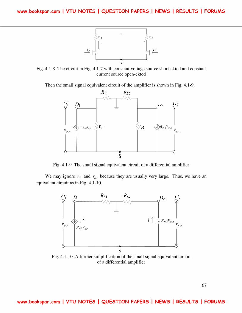
67
Fig. 4.1-8 The circuit in Fig. 4.1-7 with constant voltage source short-ckted and constant
current source open-ckted
Then the small signal equivalent circuit of the amplifier is shown in Fig. 4.1-9.
sgv1
sgv2
sgm vg11 sgm vg
22
Fig. 4.1-9 The small signal equivalent circuit of a differential amplifier
We may ignore 1or and 2or because they are usually very large. Thus, we have an
equivalent circuit as in Fig. 4.1-10.
sgv1
sgv2
sgm vg11
sgm vg22
Fig. 4.1-10 A further simplification of the small signal equivalent circuit
of a differential amplifier
www.bookspar.com | VTU NOTES | QUESTION PAPERS | NEWS | RESULTS | FORUMS
www.bookspar.com | VTU NOTES | QUESTION PAPERS | NEWS | RESULTS | FORUMS
68
We should note here that sgi vv11 ≠ and sgi vv
22 ≠ because the voltage at S is not
grounded. But,
sgsgsgsgggiiin vvvvvvvvvvv21
)( 212121 −=−−−=−=−= (4.1-5)
We further have
sgmsgm vgvgi2211
−== . (4.1-6)
Thus, we have:
1
1
m
sgg
iv = (4.1-7)
2
2
m
sgg
iv
−= (4.1-8)
and
+=−=
21
21
11
mm
sgsgingg
ivvv (4.1-9)
Let us assume that 21 mmm ggg == . We have
m
ing
iv
2= (4.1-10)
and finally,
in
m vg
i2
= (4.1-11)
Combining Equations (4.1-4) and (4.1-11), we have:
inLmout vRgv = (4.1-12)
The gain of the amplifier is as follows:
Lm
in
out Rgv
va == (4.1-13)
www.bookspar.com | VTU NOTES | QUESTION PAPERS | NEWS | RESULTS | FORUMS
www.bookspar.com | VTU NOTES | QUESTION PAPERS | NEWS | RESULTS | FORUMS
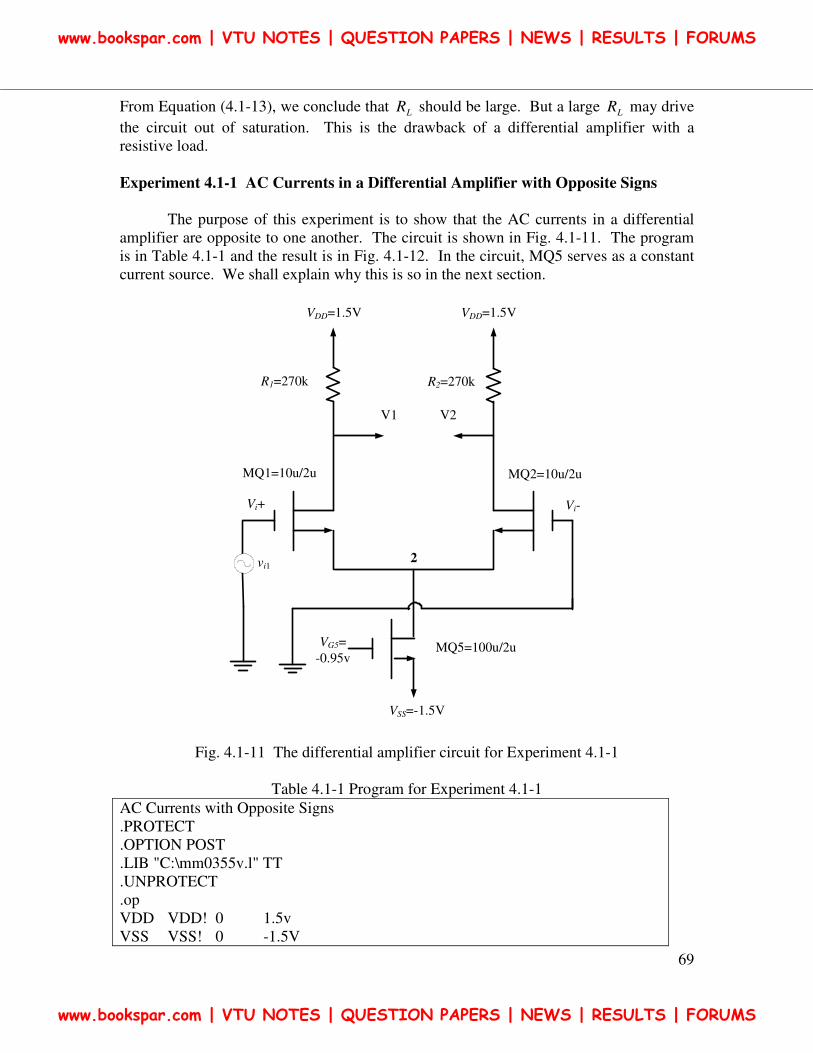
69
From Equation (4.1-13), we conclude that LR should be large. But a large LR may drive
the circuit out of saturation. This is the drawback of a differential amplifier with a
resistive load.
Experiment 4.1-1 AC Currents in a Differential Amplifier with Opposite Signs
The purpose of this experiment is to show that the AC currents in a differential
amplifier are opposite to one another. The circuit is shown in Fig. 4.1-11. The program
is in Table 4.1-1 and the result is in Fig. 4.1-12. In the circuit, MQ5 serves as a constant
current source. We shall explain why this is so in the next section.
VDD=1.5V
V2
MQ1=10u/2u MQ2=10u/2u
VG5=
-0.95v
VSS=-1.5V
VDD=1.5V
2
V1
Vi+
R1=270k R2=270k
MQ5=100u/2u
Vi-
vi1
Fig. 4.1-11 The differential amplifier circuit for Experiment 4.1-1
Table 4.1-1 Program for Experiment 4.1-1
AC Currents with Opposite Signs
.PROTECT
.OPTION POST
.LIB "C:\mm0355v.l" TT
.UNPROTECT
.op
VDD VDD! 0 1.5v
VSS VSS! 0 -1.5V
www.bookspar.com | VTU NOTES | QUESTION PAPERS | NEWS | RESULTS | FORUMS
www.bookspar.com | VTU NOTES | QUESTION PAPERS | NEWS | RESULTS | FORUMS
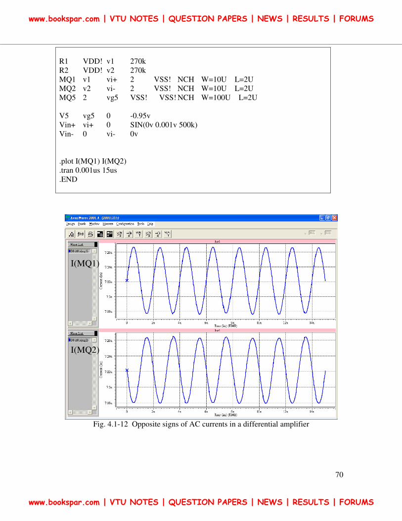
70
R1 VDD! v1 270k
R2 VDD! v2 270k
MQ1 v1 vi+ 2 VSS! NCH W=10U L=2U
MQ2 v2 vi- 2 VSS! NCH W=10U L=2U
MQ5 2 vg5 VSS! VSS! NCH W=100U L=2U
V5 vg5 0 -0.95v
Vin+ vi+ 0 SIN(0v 0.001v 500k)
Vin- 0 vi- 0v
.plot I(MQ1) I(MQ2)
.tran 0.001us 15us
.END
Fig. 4.1-12 Opposite signs of AC currents in a differential amplifier
I(MQ1)
I(MQ2)
www.bookspar.com | VTU NOTES | QUESTION PAPERS | NEWS | RESULTS | FORUMS
www.bookspar.com | VTU NOTES | QUESTION PAPERS | NEWS | RESULTS | FORUMS
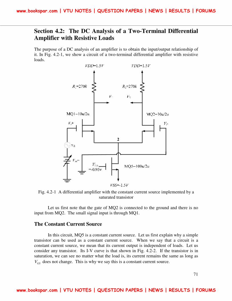
71
Section 4.2: The DC Analysis of a Two-Terminal Differential
Amplifier with Resistive Loads
The purpose of a DC analysis of an amplifier is to obtain the input/output relationship of
it. In Fig. 4.2-1, we show a circuit of a two-terminal differential amplifier with resistive
loads.
Fig. 4.2-1 A differential amplifier with the constant current source implemented by a
saturated transistor
Let us first note that the gate of MQ2 is connected to the ground and there is no
input from MQ2. The small signal input is through MQ1.
The Constant Current Source
In this circuit, MQ5 is a constant current source. Let us first explain why a simple
transistor can be used as a constant current source. When we say that a circuit is a
constant current source, we mean that its current output is independent of loads. Let us
consider any transistor. Its I-V curve is that shown in Fig. 4.2-2. If the transistor is in
saturation, we can see no matter what the load is, its current remains the same as long as
GSV does not change. This is why we say this is a constant current source.
www.bookspar.com | VTU NOTES | QUESTION PAPERS | NEWS | RESULTS | FORUMS
www.bookspar.com | VTU NOTES | QUESTION PAPERS | NEWS | RESULTS | FORUMS
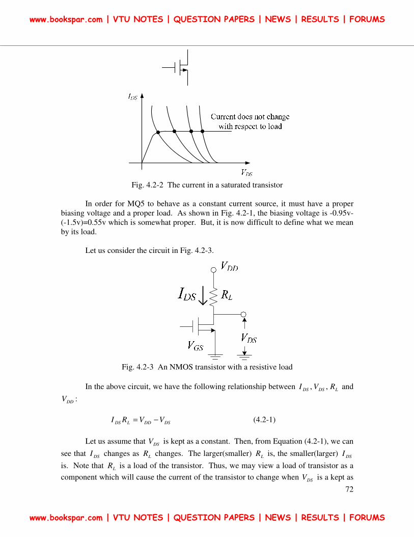
72
Fig. 4.2-2 The current in a saturated transistor
In order for MQ5 to behave as a constant current source, it must have a proper
biasing voltage and a proper load. As shown in Fig. 4.2-1, the biasing voltage is -0.95v-
(-1.5v)=0.55v which is somewhat proper. But, it is now difficult to define what we mean
by its load.
Let us consider the circuit in Fig. 4.2-3.
Fig. 4.2-3 An NMOS transistor with a resistive load
In the above circuit, we have the following relationship between LDSDS RVI ,, and
DDV :
DSDDLDS VVRI −= (4.2-1)
Let us assume that DSV is kept as a constant. Then, from Equation (4.2-1), we can
see that DSI changes as LR changes. The larger(smaller) LR is, the smaller(larger) DSI
is. Note that LR is a load of the transistor. Thus, we may view a load of transistor as a
component which will cause the current of the transistor to change when DSV is a kept as
www.bookspar.com | VTU NOTES | QUESTION PAPERS | NEWS | RESULTS | FORUMS
www.bookspar.com | VTU NOTES | QUESTION PAPERS | NEWS | RESULTS | FORUMS
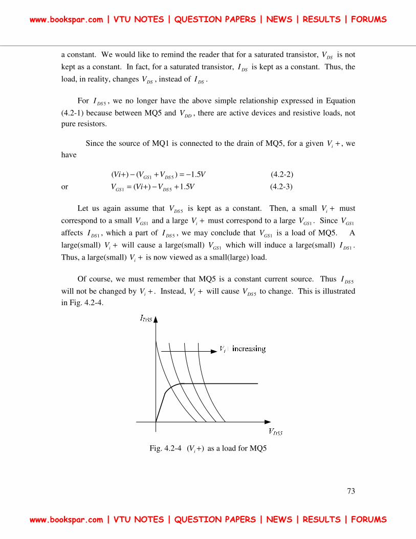
73
a constant. We would like to remind the reader that for a saturated transistor, DSV is not
kept as a constant. In fact, for a saturated transistor, DSI is kept as a constant. Thus, the
load, in reality, changes DSV , instead of DSI .
For 5DSI , we no longer have the above simple relationship expressed in Equation
(4.2-1) because between MQ5 and DDV , there are active devices and resistive loads, not
pure resistors.
Since the source of MQ1 is connected to the drain of MQ5, for a given +iV , we
have
VVVVi DSGS 5.1)()( 51 −=+−+ (4.2-2)
or VVViV DSGS 5.1)( 51 +−+= (4.2-3)
Let us again assume that 5DSV is kept as a constant. Then, a small +iV must
correspond to a small 1GSV and a large +iV must correspond to a large 1GSV . Since 1GSV
affects 1DSI , which a part of 5DSI , we may conclude that 1GSV is a load of MQ5. A
large(small) +iV will cause a large(small) 1GSV which will induce a large(small) 1DSI .
Thus, a large(small) +iV is now viewed as a small(large) load.
Of course, we must remember that MQ5 is a constant current source. Thus 5DSI
will not be changed by +iV . Instead, +iV will cause 5DSV to change. This is illustrated
in Fig. 4.2-4.
Fig. 4.2-4 )( +iV as a load for MQ5
www.bookspar.com | VTU NOTES | QUESTION PAPERS | NEWS | RESULTS | FORUMS
www.bookspar.com | VTU NOTES | QUESTION PAPERS | NEWS | RESULTS | FORUMS
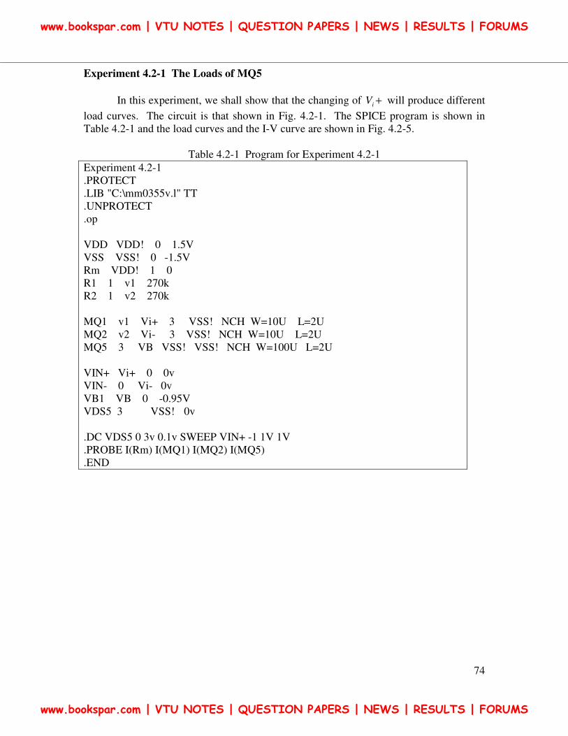
74
Experiment 4.2-1 The Loads of MQ5
In this experiment, we shall show that the changing of +iV will produce different
load curves. The circuit is that shown in Fig. 4.2-1. The SPICE program is shown in
Table 4.2-1 and the load curves and the I-V curve are shown in Fig. 4.2-5.
Table 4.2-1 Program for Experiment 4.2-1
Experiment 4.2-1
.PROTECT
.LIB "C:\mm0355v.l" TT
.UNPROTECT
.op
VDD VDD! 0 1.5V
VSS VSS! 0 -1.5V
Rm VDD! 1 0
R1 1 v1 270k
R2 1 v2 270k
MQ1 v1 Vi+ 3 VSS! NCH W=10U L=2U
MQ2 v2 Vi- 3 VSS! NCH W=10U L=2U
MQ5 3 VB VSS! VSS! NCH W=100U L=2U
VIN+ Vi+ 0 0v
VIN- 0 Vi- 0v
VB1 VB 0 -0.95V
VDS5 3 VSS! 0v
.DC VDS5 0 3v 0.1v SWEEP VIN+ -1 1V 1V
.PROBE I(Rm) I(MQ1) I(MQ2) I(MQ5)
.END
www.bookspar.com | VTU NOTES | QUESTION PAPERS | NEWS | RESULTS | FORUMS
www.bookspar.com | VTU NOTES | QUESTION PAPERS | NEWS | RESULTS | FORUMS
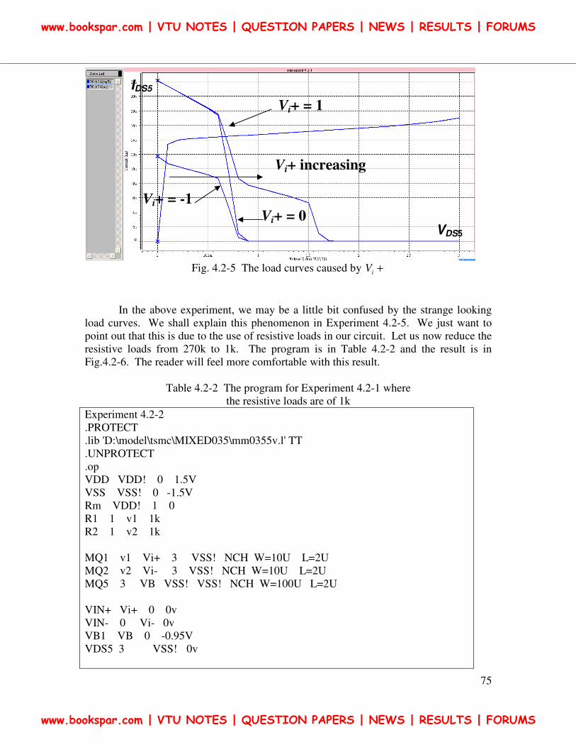
75
Fig. 4.2-5 The load curves caused by +iV
In the above experiment, we may be a little bit confused by the strange looking
load curves. We shall explain this phenomenon in Experiment 4.2-5. We just want to
point out that this is due to the use of resistive loads in our circuit. Let us now reduce the
resistive loads from 270k to 1k. The program is in Table 4.2-2 and the result is in
Fig.4.2-6. The reader will feel more comfortable with this result.
Table 4.2-2 The program for Experiment 4.2-1 where
the resistive loads are of 1k
Experiment 4.2-2
.PROTECT
.lib 'D:\model\tsmc\MIXED035\mm0355v.l' TT
.UNPROTECT
.op
VDD VDD! 0 1.5V
VSS VSS! 0 -1.5V
Rm VDD! 1 0
R1 1 v1 1k
R2 1 v2 1k
MQ1 v1 Vi+ 3 VSS! NCH W=10U L=2U
MQ2 v2 Vi- 3 VSS! NCH W=10U L=2U
MQ5 3 VB VSS! VSS! NCH W=100U L=2U
VIN+ Vi+ 0 0v
VIN- 0 Vi- 0v
VB1 VB 0 -0.95V
VDS5 3 VSS! 0v
VDS5
IDS5
Vi+ increasing
Vi+ = -1
Vi+ = 0
Vi+ = 1
www.bookspar.com | VTU NOTES | QUESTION PAPERS | NEWS | RESULTS | FORUMS
www.bookspar.com | VTU NOTES | QUESTION PAPERS | NEWS | RESULTS | FORUMS
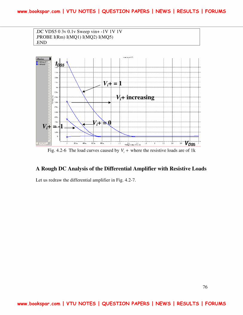
76
.DC VDS5 0 3v 0.1v Sweep vin+ -1V 1V 1V
.PROBE I(Rm) I(MQ1) I(MQ2) I(MQ5)
.END
Fig. 4.2-6 The load curves caused by +iV where the resistive loads are of 1k
A Rough DC Analysis of the Differential Amplifier with Resistive Loads
Let us redraw the differential amplifier in Fig. 4.2-7.
VDS5
IDS5
Vi+ increasing
Vi+ = -1 Vi+ = 0
Vi+ = 1
www.bookspar.com | VTU NOTES | QUESTION PAPERS | NEWS | RESULTS | FORUMS
www.bookspar.com | VTU NOTES | QUESTION PAPERS | NEWS | RESULTS | FORUMS
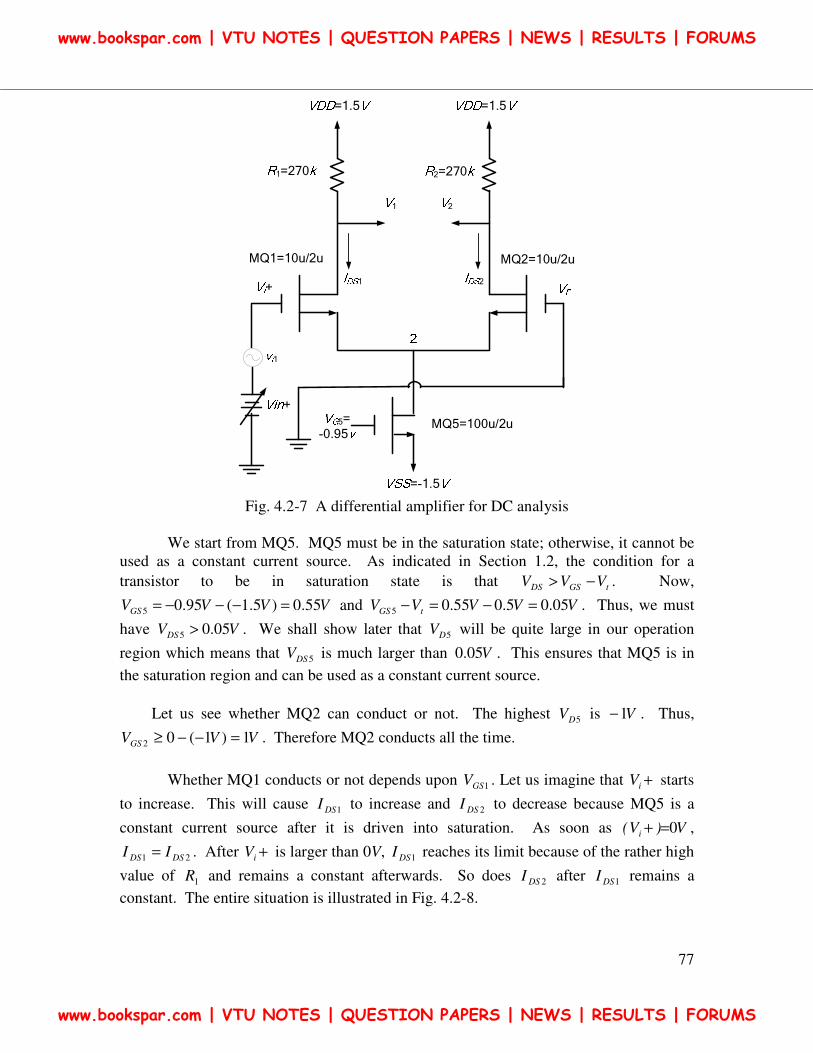
77
=1.5
2
MQ1=10u/2u MQ2=10u/2u
5=
-0.95
=-1.5
=1.5
+
1
+
1=270 2=270
MQ5=100u/2u
-
1
1 2
Fig. 4.2-7 A differential amplifier for DC analysis
We start from MQ5. MQ5 must be in the saturation state; otherwise, it cannot be
used as a constant current source. As indicated in Section 1.2, the condition for a
transistor to be in saturation state is that tGSDS VVV −> . Now,
VVVVGS 55.0)5.1(95.05 =−−−= and VVVVV tGS 05.05.055.05 =−=− . Thus, we must
have VVDS 05.05 > . We shall show later that 5DV will be quite large in our operation
region which means that 5DSV is much larger than V05.0 . This ensures that MQ5 is in
the saturation region and can be used as a constant current source.
Let us see whether MQ2 can conduct or not. The highest 5DV is V1− . Thus,
VVVGS 1)1(02 =−−≥ . Therefore MQ2 conducts all the time.
Whether MQ1 conducts or not depends upon 1GSV . Let us imagine that +iV starts
to increase. This will cause 1DSI to increase and 2DSI to decrease because MQ5 is a
constant current source after it is driven into saturation. As soon as V)V( i 0=+ ,
21 DSDS II = . After +iV is larger than 0V, 1DSI reaches its limit because of the rather high
value of 1R and remains a constant afterwards. So does 2DSI after 1DSI remains a
constant. The entire situation is illustrated in Fig. 4.2-8.
www.bookspar.com | VTU NOTES | QUESTION PAPERS | NEWS | RESULTS | FORUMS
www.bookspar.com | VTU NOTES | QUESTION PAPERS | NEWS | RESULTS | FORUMS
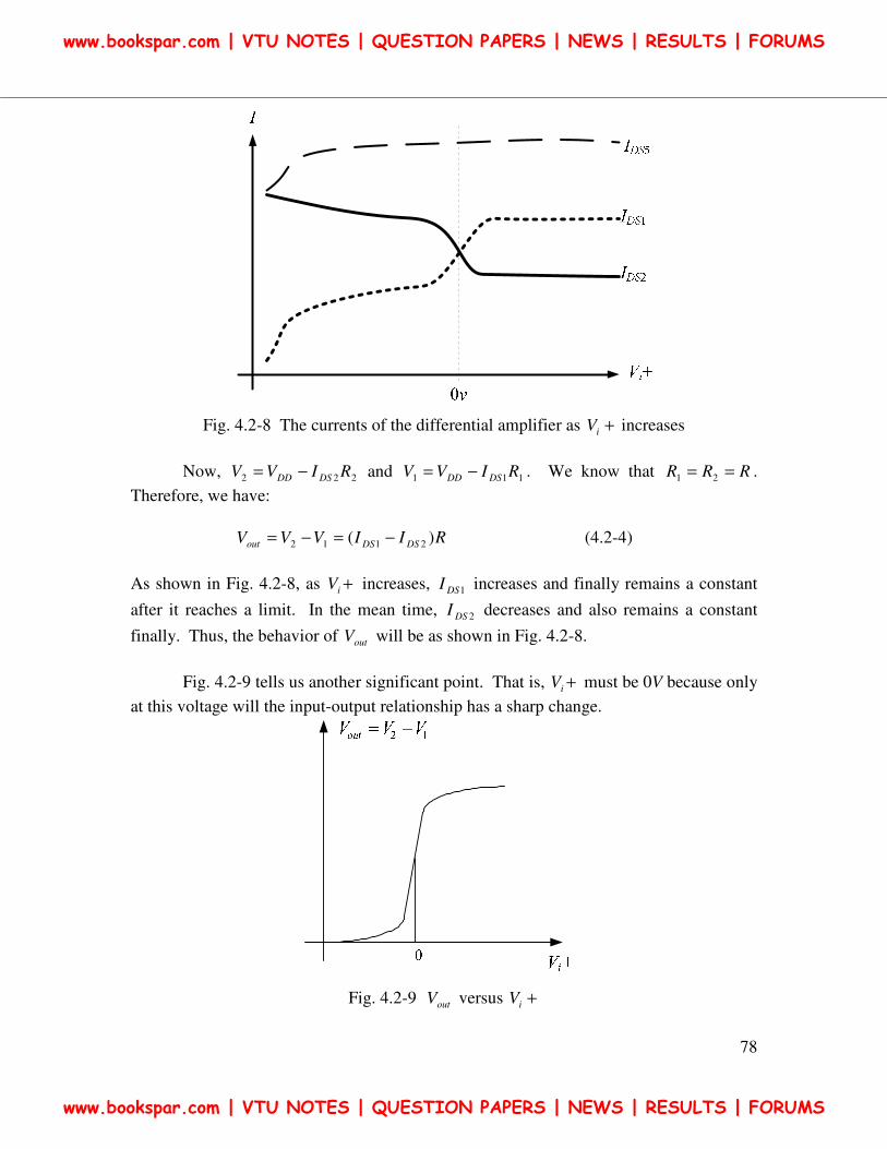
78
Fig. 4.2-8 The currents of the differential amplifier as +iV increases
Now, 222 RIVV DSDD −= and 111 RIVV DSDD −= . We know that RRR == 21 .
Therefore, we have:
RIIVVV DSDSout )( 2112 −=−= (4.2-4)
As shown in Fig. 4.2-8, as +iV increases, 1DSI increases and finally remains a constant
after it reaches a limit. In the mean time, 2DSI decreases and also remains a constant
finally. Thus, the behavior of outV will be as shown in Fig. 4.2-8.
Fig. 4.2-9 tells us another significant point. That is, +iV must be 0V because only
at this voltage will the input-output relationship has a sharp change.
Fig. 4.2-9 outV versus +iV
www.bookspar.com | VTU NOTES | QUESTION PAPERS | NEWS | RESULTS | FORUMS
www.bookspar.com | VTU NOTES | QUESTION PAPERS | NEWS | RESULTS | FORUMS
79
We can see that there is no sharp jump of outV as +iV increases. We shall see
later that this differential amplifier will be modified such that there will be a sharp jump
of outV .
A More Detailed DC Analysis of the Differential Amplifier
Consider the differential amplifier in Fig. 4.2-7 again. In the above DC analysis of the
circuit, we view the problem almost entirely from the viewpoint of the constant current
source. We casually claimed that as +iV increases, 1GSV increases as if 15 SD VV = is kept
a constant. In reality, the drain of MQ5, which is also the source of MQ1, is not
connected to any power supply. Therefore, 15 SD VV = may change. We simply cannot
assume that it is kept as a constant.
We pointed out before that a larger +iV will correspond to a smaller load for MQ5.
The load curves and the I-V curve are now shown in Fig. 4.2-11. Note that a small load
means a higher +iV .
Fig. 4.2-11 The increasing of 5DSV due to the increasing of +iV
From Fig. 4.2-10, we conclude that as +iV increases, 5DSV increases. Since
VVS 5.15 −= which is a constant, we may conclude that as +iV increases, 5DV increases
accordingly. Luckily, 5DSV does not increase as fast as +iV does. We thus can make the
claim that as +iV increases, 51 DiGS V)V(V −+= increases. This will increase the current in
MQ1.
Previously, we indicated that 2DSI will decrease as 1DSI increases because MQ5 is
a constant current source. We shall now explain this phenomenon from the viewpoint of
www.bookspar.com | VTU NOTES | QUESTION PAPERS | NEWS | RESULTS | FORUMS
www.bookspar.com | VTU NOTES | QUESTION PAPERS | NEWS | RESULTS | FORUMS
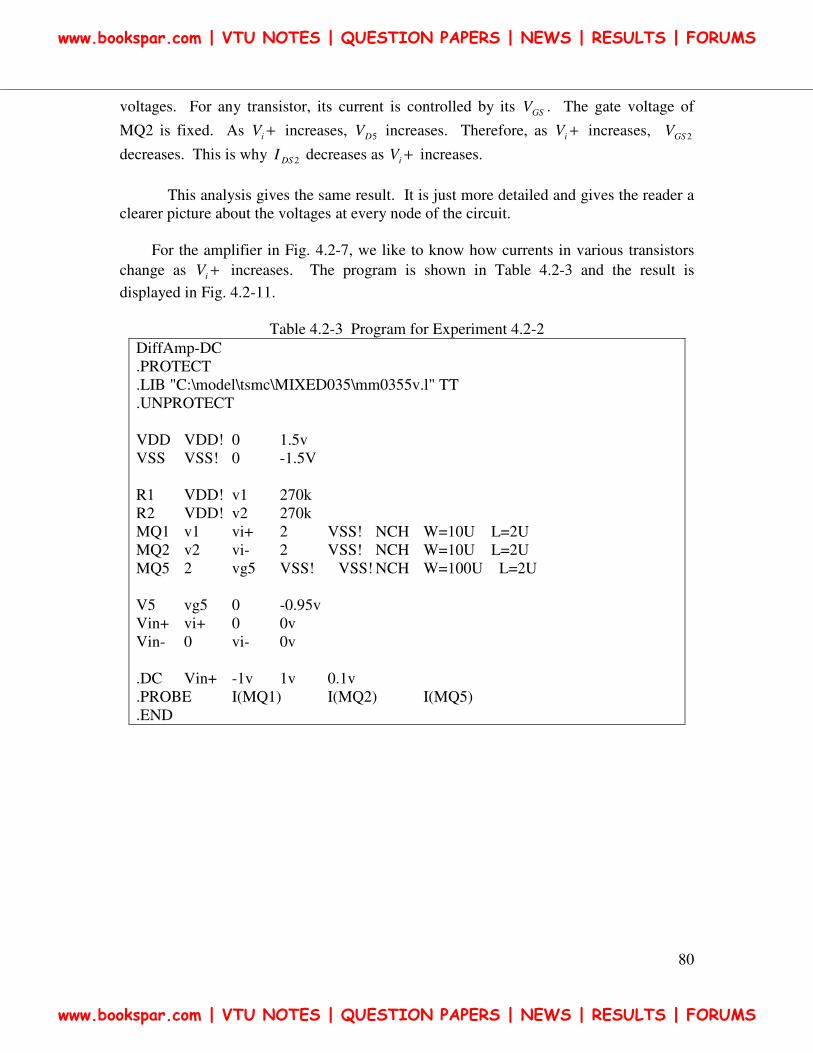
80
voltages. For any transistor, its current is controlled by its GSV . The gate voltage of
MQ2 is fixed. As +iV increases, 5DV increases. Therefore, as +iV increases, 2GSV
decreases. This is why 2DSI decreases as +iV increases.
This analysis gives the same result. It is just more detailed and gives the reader a
clearer picture about the voltages at every node of the circuit.
For the amplifier in Fig. 4.2-7, we like to know how currents in various transistors
change as +iV increases. The program is shown in Table 4.2-3 and the result is
displayed in Fig. 4.2-11.
Table 4.2-3 Program for Experiment 4.2-2
DiffAmp-DC
.PROTECT
.LIB "C:\model\tsmc\MIXED035\mm0355v.l" TT
.UNPROTECT
VDD VDD! 0 1.5v
VSS VSS! 0 -1.5V
R1 VDD! v1 270k
R2 VDD! v2 270k
MQ1 v1 vi+ 2 VSS! NCH W=10U L=2U
MQ2 v2 vi- 2 VSS! NCH W=10U L=2U
MQ5 2 vg5 VSS! VSS! NCH W=100U L=2U
V5 vg5 0 -0.95v
Vin+ vi+ 0 0v
Vin- 0 vi- 0v
.DC Vin+ -1v 1v 0.1v
.PROBE I(MQ1) I(MQ2) I(MQ5)
.END
www.bookspar.com | VTU NOTES | QUESTION PAPERS | NEWS | RESULTS | FORUMS
www.bookspar.com | VTU NOTES | QUESTION PAPERS | NEWS | RESULTS | FORUMS
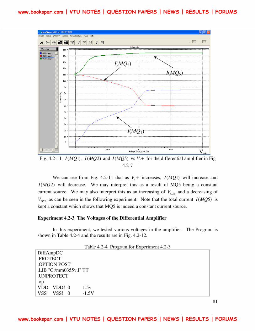
81
Fig. 4.2-11 )1(MQI , )2(MQI and )5(MQI vs +iV for the differential amplifier in Fig
4.2-7
We can see from Fig. 4.2-11 that as +iV increases, )1(MQI will increase and
)2(MQI will decrease. We may interpret this as a result of MQ5 being a constant
current source. We may also interpret this as an increasing of 1GSV and a decreasing of
2GSV as can be seen in the following experiment. Note that the total current )5(MQI is
kept a constant which shows that MQ5 is indeed a constant current source.
Experiment 4.2-3 The Voltages of the Differential Amplifier
In this experiment, we tested various voltages in the amplifier. The Program is
shown in Table 4.2-4 and the results are in Fig. 4.2-12.
Table 4.2-4 Program for Experiment 4.2-3
DiffAmpDC
.PROTECT
.OPTION POST
.LIB "C:\mm0355v.l" TT
.UNPROTECT
.op
VDD VDD! 0 1.5v
VSS VSS! 0 -1.5V
I(MQ5)
I(MQ2)
I(MQ1)
Vi+
www.bookspar.com | VTU NOTES | QUESTION PAPERS | NEWS | RESULTS | FORUMS
www.bookspar.com | VTU NOTES | QUESTION PAPERS | NEWS | RESULTS | FORUMS
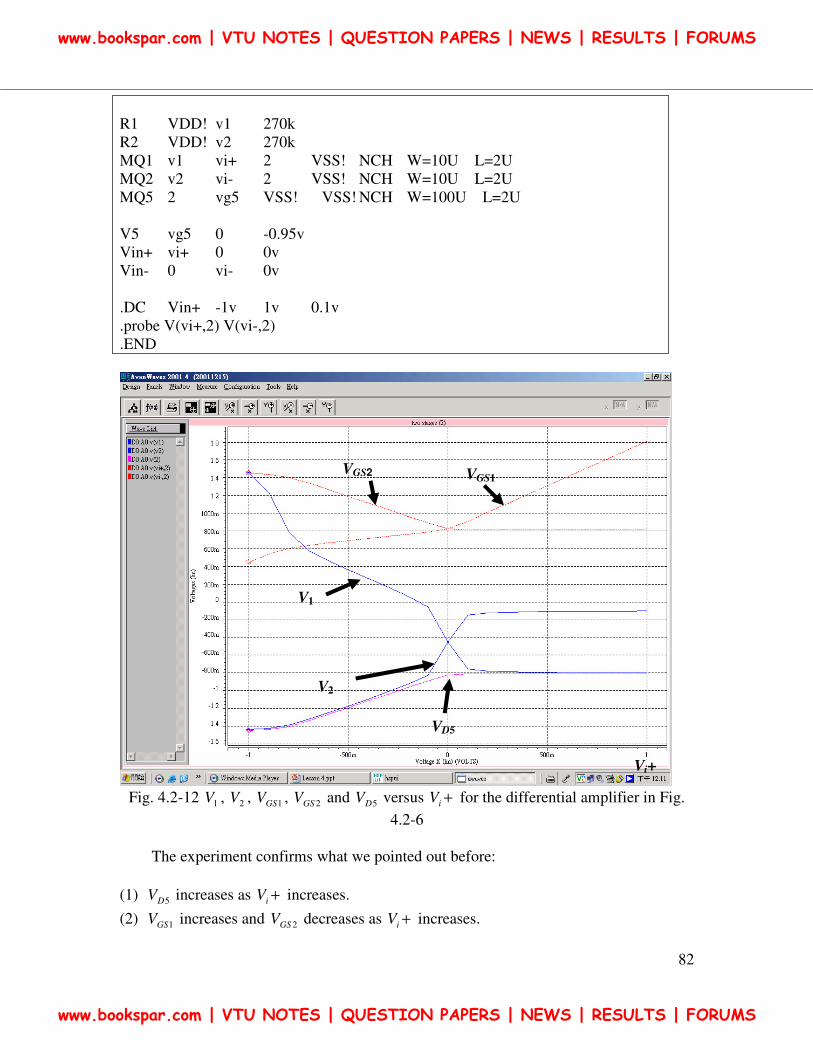
82
R1 VDD! v1 270k
R2 VDD! v2 270k
MQ1 v1 vi+ 2 VSS! NCH W=10U L=2U
MQ2 v2 vi- 2 VSS! NCH W=10U L=2U
MQ5 2 vg5 VSS! VSS! NCH W=100U L=2U
V5 vg5 0 -0.95v
Vin+ vi+ 0 0v
Vin- 0 vi- 0v
.DC Vin+ -1v 1v 0.1v
.probe V(vi+,2) V(vi-,2)
.END
Fig. 4.2-12 1V , 2V , 1GSV , 2GSV and 5DV versus +iV for the differential amplifier in Fig.
4.2-6
The experiment confirms what we pointed out before:
(1) 5DV increases as +iV increases.
(2) 1GSV increases and 2GSV decreases as +iV increases.
V1
VD5
Vi+
V2
VGS2 VGS1
www.bookspar.com | VTU NOTES | QUESTION PAPERS | NEWS | RESULTS | FORUMS
www.bookspar.com | VTU NOTES | QUESTION PAPERS | NEWS | RESULTS | FORUMS
83
(3) 2V increases and 1V decreases as +iV increases.
The relationship between +iV and 12 VVVout −= is shown in Fig. 4.2-12.
Fig
. 4.2-13 outV vs +iV for the differential amplifier in Fig 4.2-6
Since there is not a very sharp in Fig. 4.2-13, this differential amplifier does not
have a high gain, as expected. A much improved differential amplifier with active loads
will be introduced in the next section.
Let us take a look at Fig. 4.2-12 again. Note that 5DV does not increase all the
time. This can be explained by going back to Fig. 4.2-10. It reaches a maximum and
remains a constant afterwards. We shall now try to explain why 5DV has such a behavior.
First of all, from the circuit in Fig. 4.2-7, we have:
5 1 1D DSV V V+ = (4.2-5)
From (4.2-5), we have
5 1 1D DSV V V= − (4.2-6)
Equation (4.2-6) indicates that 5DV is bounded by 1V . The maximum of 5DV is reached
when 01 =DSV . Under such circumstances, 15 VVD = .
www.bookspar.com | VTU NOTES | QUESTION PAPERS | NEWS | RESULTS | FORUMS
www.bookspar.com | VTU NOTES | QUESTION PAPERS | NEWS | RESULTS | FORUMS
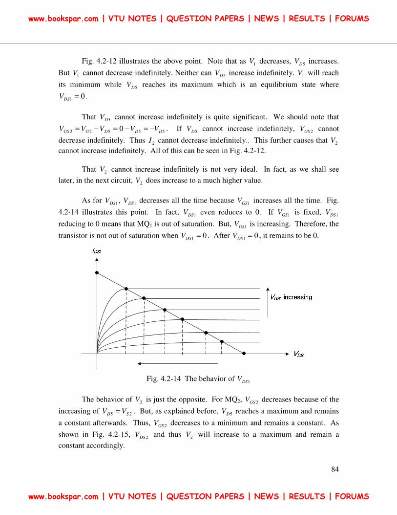
84
Fig. 4.2-12 illustrates the above point. Note that as 1V decreases, 5DV increases.
But 1V cannot decrease indefinitely. Neither can 5DV increase indefinitely. 1V will reach
its minimum while 5DV reaches its maximum which is an equilibrium state where
01 =DSV .
That 5DV cannot increase indefinitely is quite significant. We should note that
55522 0 DDDGGS VVVVV −=−=−= . If 5DV cannot increase indefinitely, 2GSV cannot
decrease indefinitely. Thus 2I cannot decrease indefinitely.. This further causes that 2V
cannot increase indefinitely. All of this can be seen in Fig. 4.2-12.
That 2V cannot increase indefinitely is not very ideal. In fact, as we shall see
later, in the next circuit, 2V does increase to a much higher value.
As for 1DSV , 1DSV decreases all the time because 1GSV increases all the time. Fig.
4.2-14 illustrates this point. In fact, 1DSV even reduces to 0. If 1GSV is fixed, 1DSV
reducing to 0 means that MQ1 is out of saturation. But, 1GSV is increasing. Therefore, the
transistor is not out of saturation when 01 =DSV . After 01 =DSV , it remains to be 0.
Fig. 4.2-14 The behavior of 1DSV
The behavior of 2V is just the opposite. For MQ2, 2GSV decreases because of the
increasing of 25 SD VV = . But, as explained before, 5DV reaches a maximum and remains
a constant afterwards. Thus, 2GSV decreases to a minimum and remains a constant. As
shown in Fig. 4.2-15, 2DSV and thus 2V will increase to a maximum and remain a
constant accordingly.
www.bookspar.com | VTU NOTES | QUESTION PAPERS | NEWS | RESULTS | FORUMS
www.bookspar.com | VTU NOTES | QUESTION PAPERS | NEWS | RESULTS | FORUMS
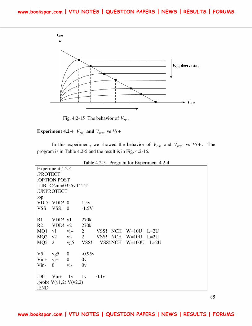
85
Fig. 4.2-15 The behavior of 2DSV
Experiment 4.2-4 1DSV and 2DSV vs +Vi
In this experiment, we showed the behavior of 1DSV and 2DSV vs +Vi . The
program is in Table 4.2-5 and the result is in Fig. 4.2-16.
Table 4.2-5 Program for Experiment 4.2-4
Experiment 4.2-4
.PROTECT
.OPTION POST
.LIB "C:\mm0355v.l" TT
.UNPROTECT
.op
VDD VDD! 0 1.5v
VSS VSS! 0 -1.5V
R1 VDD! v1 270k
R2 VDD! v2 270k
MQ1 v1 vi+ 2 VSS! NCH W=10U L=2U
MQ2 v2 vi- 2 VSS! NCH W=10U L=2U
MQ5 2 vg5 VSS! VSS! NCH W=100U L=2U
V5 vg5 0 -0.95v
Vin+ vi+ 0 0v
Vin- 0 vi- 0v
.DC Vin+ -1v 1v 0.1v
.probe V(v1,2) V(v2,2)
.END
www.bookspar.com | VTU NOTES | QUESTION PAPERS | NEWS | RESULTS | FORUMS
www.bookspar.com | VTU NOTES | QUESTION PAPERS | NEWS | RESULTS | FORUMS
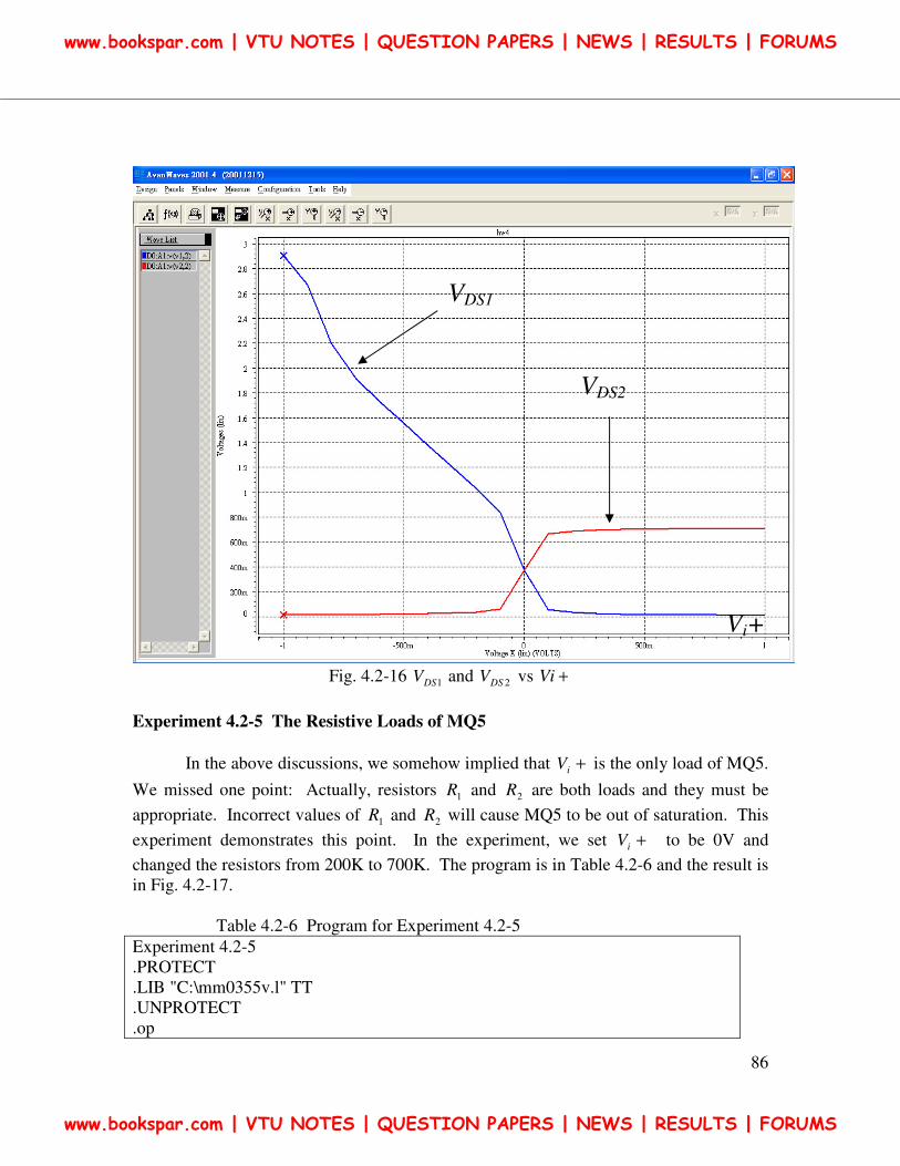
86
Fig. 4.2-16 1DSV and 2DSV vs +Vi
Experiment 4.2-5 The Resistive Loads of MQ5
In the above discussions, we somehow implied that +iV is the only load of MQ5.
We missed one point: Actually, resistors 1R and 2R are both loads and they must be
appropriate. Incorrect values of 1R and 2R will cause MQ5 to be out of saturation. This
experiment demonstrates this point. In the experiment, we set +iV to be 0V and
changed the resistors from 200K to 700K. The program is in Table 4.2-6 and the result is
in Fig. 4.2-17.
Table 4.2-6 Program for Experiment 4.2-5
Experiment 4.2-5
.PROTECT
.LIB "C:\mm0355v.l" TT
.UNPROTECT
.op
VDS1
VDS2
Vi+
www.bookspar.com | VTU NOTES | QUESTION PAPERS | NEWS | RESULTS | FORUMS
www.bookspar.com | VTU NOTES | QUESTION PAPERS | NEWS | RESULTS | FORUMS
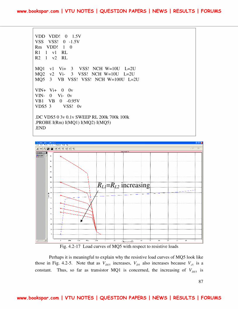
87
VDD VDD! 0 1.5V
VSS VSS! 0 -1.5V
Rm VDD! 1 0
R1 1 v1 RL
R2 1 v2 RL
MQ1 v1 Vi+ 3 VSS! NCH W=10U L=2U
MQ2 v2 Vi- 3 VSS! NCH W=10U L=2U
MQ5 3 VB VSS! VSS! NCH W=100U L=2U
VIN+ Vi+ 0 0v
VIN- 0 Vi- 0v
VB1 VB 0 -0.95V
VDS5 3 VSS! 0v
.DC VDS5 0 3v 0.1v SWEEP RL 200k 700k 100k
.PROBE I(Rm) I(MQ1) I(MQ2) I(MQ5)
.END
Fig. 4.2-17 Load curves of MQ5 with respect to resistive loads
Perhaps it is meaningful to explain why the resistive load curves of MQ5 look like
those in Fig. 4.2-5. Note that as 5DSV increases, 5DV also increases because 5sV is a
constant. Thus, so far as transistor MQ1 is concerned, the increasing of 5DSV is
RL1=RL2 increasing
www.bookspar.com | VTU NOTES | QUESTION PAPERS | NEWS | RESULTS | FORUMS
www.bookspar.com | VTU NOTES | QUESTION PAPERS | NEWS | RESULTS | FORUMS
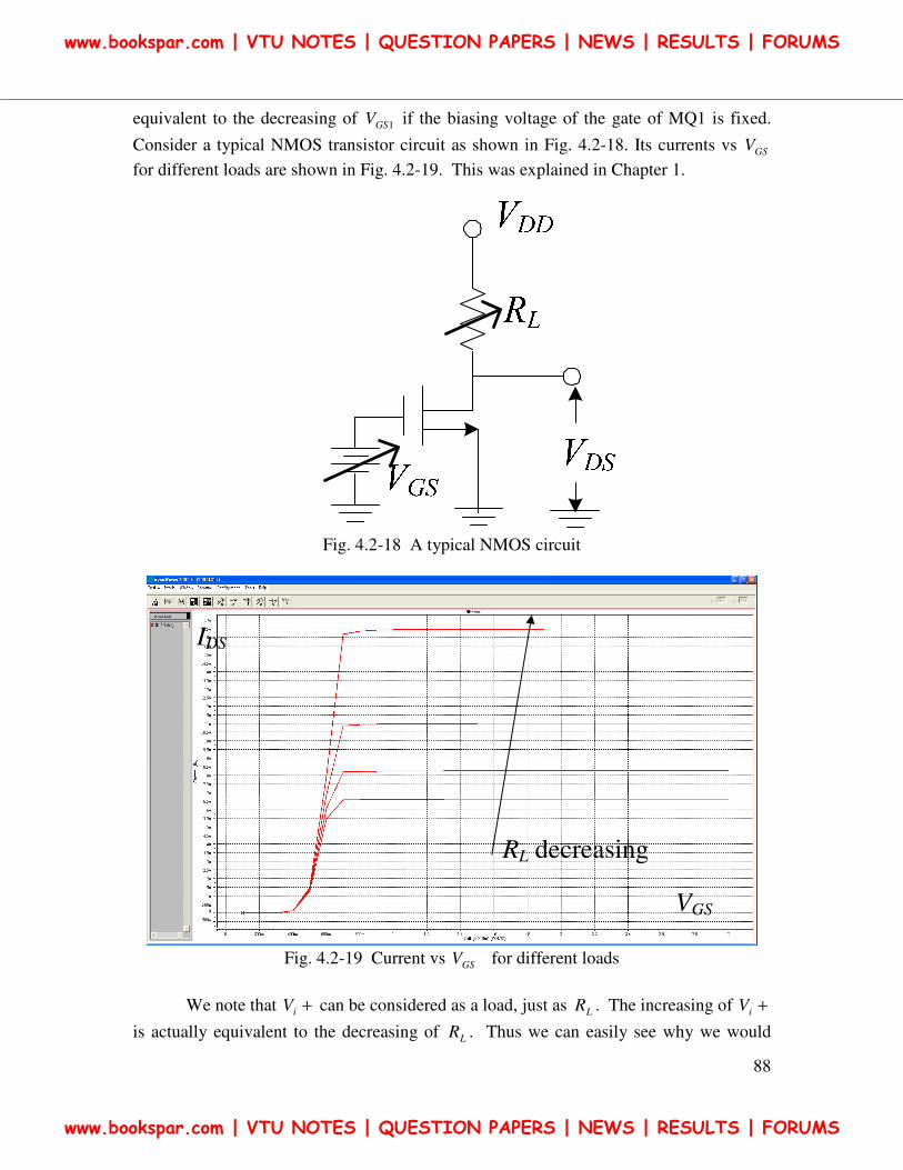
88
equivalent to the decreasing of 1GSV if the biasing voltage of the gate of MQ1 is fixed.
Consider a typical NMOS transistor circuit as shown in Fig. 4.2-18. Its currents vs GSV
for different loads are shown in Fig. 4.2-19. This was explained in Chapter 1.
Fig. 4.2-18 A typical NMOS circuit
Fig. 4.2-19 Current vs GSV for different loads
We note that +iV can be considered as a load, just as LR . The increasing of +iV
is actually equivalent to the decreasing of LR . Thus we can easily see why we would
IDS
VGS
RL decreasing
www.bookspar.com | VTU NOTES | QUESTION PAPERS | NEWS | RESULTS | FORUMS
www.bookspar.com | VTU NOTES | QUESTION PAPERS | NEWS | RESULTS | FORUMS
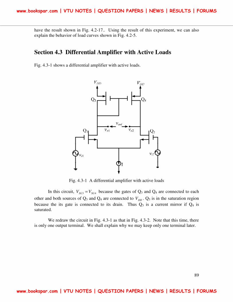
89
have the result shown in Fig. 4.2-17.. Using the result of this experiment, we can also
explain the behavior of load curves shown in Fig. 4.2-5.
Section 4.3 Differential Amplifier with Active Loads
Fig. 4.3-1 shows a differential amplifier with active loads.
Fig. 4.3-1 A differential amplifier with active loads
In this circuit, 43 SGSG VV = because the gates of Q3 and Q4 are connected to each
other and both sources of Q3 and Q4 are connected to DDV . Q3 is in the saturation region
because the its gate is connected to its drain. Thus Q3 is a current mirror if Q4 is
saturated.
We redraw the circuit in Fig. 4.3-1 as that in Fig. 4.3-2. Note that this time, there
is only one output terminal. We shall explain why we may keep only one terminal later.
www.bookspar.com | VTU NOTES | QUESTION PAPERS | NEWS | RESULTS | FORUMS
www.bookspar.com | VTU NOTES | QUESTION PAPERS | NEWS | RESULTS | FORUMS
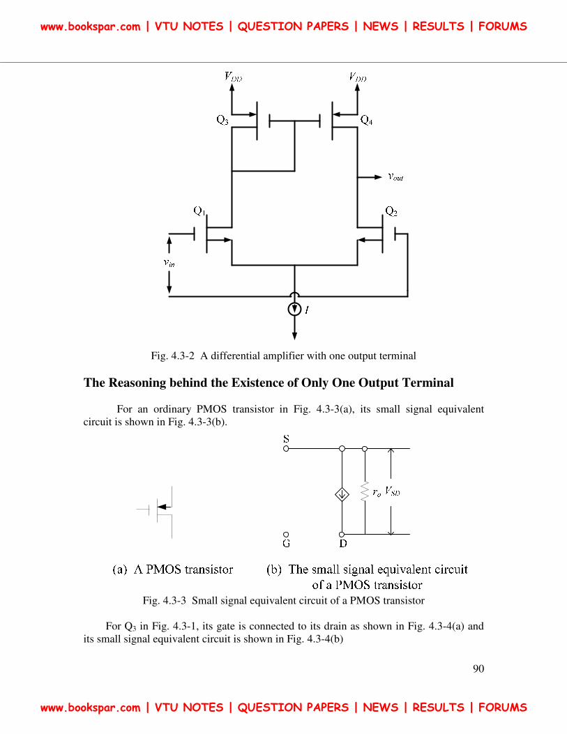
90
Fig. 4.3-2 A differential amplifier with one output terminal
The Reasoning behind the Existence of Only One Output Terminal
For an ordinary PMOS transistor in Fig. 4.3-3(a), its small signal equivalent
circuit is shown in Fig. 4.3-3(b).
Fig. 4.3-3 Small signal equivalent circuit of a PMOS transistor
For Q3 in Fig. 4.3-1, its gate is connected to its drain as shown in Fig. 4.3-4(a) and
its small signal equivalent circuit is shown in Fig. 4.3-4(b)
www.bookspar.com | VTU NOTES | QUESTION PAPERS | NEWS | RESULTS | FORUMS
www.bookspar.com | VTU NOTES | QUESTION PAPERS | NEWS | RESULTS | FORUMS
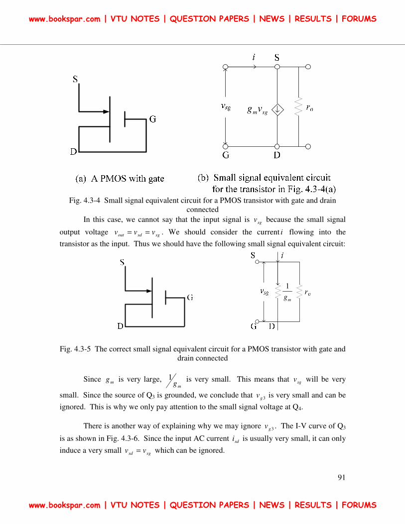
91
sgmvg
Fig. 4.3-4 Small signal equivalent circuit for a PMOS transistor with gate and drain
connected
In this case, we cannot say that the input signal is sgv because the small signal
output voltage sgsdout vvv == . We should consider the current i flowing into the
transistor as the input. Thus we should have the following small signal equivalent circuit:
mg
1
Fig. 4.3-5 The correct small signal equivalent circuit for a PMOS transistor with gate and
drain connected
Since mg is very large, mg
1 is very small. This means that sgv will be very
small. Since the source of Q3 is grounded, we conclude that 3gv is very small and can be
ignored. This is why we only pay attention to the small signal voltage at Q4.
There is another way of explaining why we may ignore 3gv . The I-V curve of Q3
is as shown in Fig. 4.3-6. Since the input AC current sdi is usually very small, it can only
induce a very small sgsd vv = which can be ignored.
www.bookspar.com | VTU NOTES | QUESTION PAPERS | NEWS | RESULTS | FORUMS
www.bookspar.com | VTU NOTES | QUESTION PAPERS | NEWS | RESULTS | FORUMS
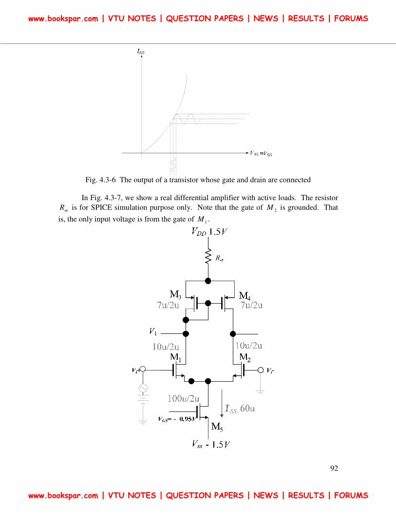
92
Fig. 4.3-6 The output of a transistor whose gate and drain are connected
In Fig. 4.3-7, we show a real differential amplifier with active loads. The resistor
mR is for SPICE simulation purpose only. Note that the gate of 2M is grounded. That
is, the only input voltage is from the gate of 1M .
www.bookspar.com | VTU NOTES | QUESTION PAPERS | NEWS | RESULTS | FORUMS
www.bookspar.com | VTU NOTES | QUESTION PAPERS | NEWS | RESULTS | FORUMS
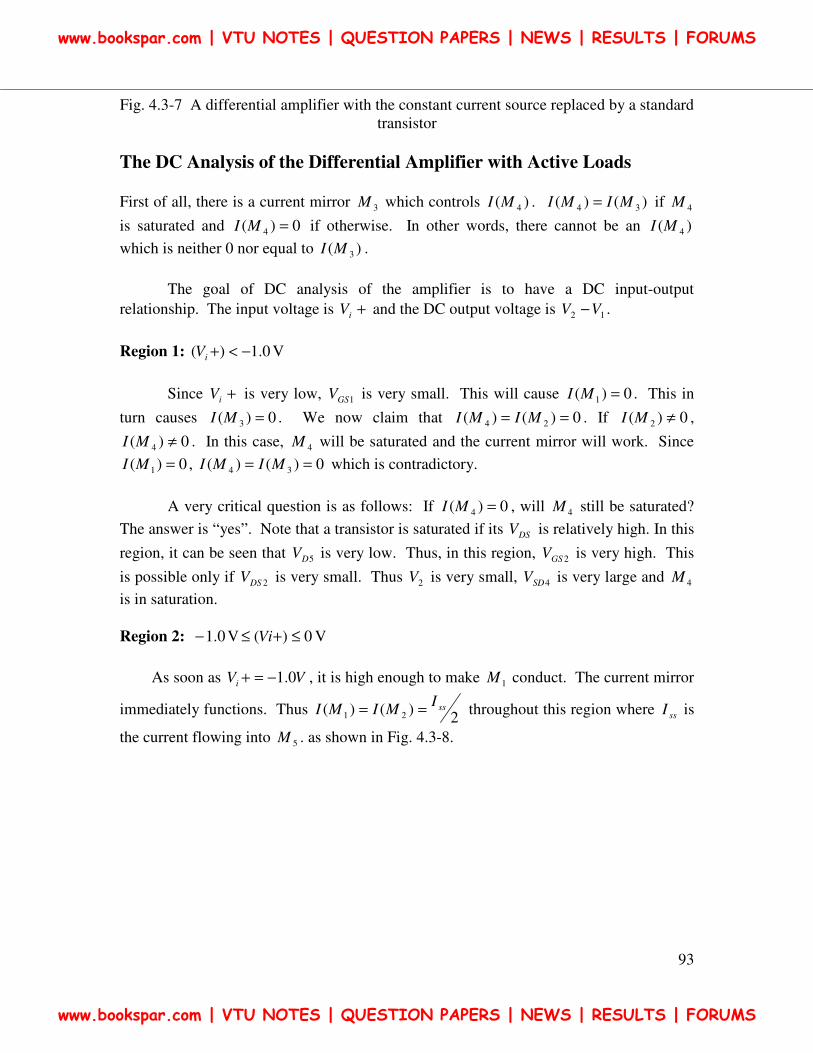
93
Fig. 4.3-7 A differential amplifier with the constant current source replaced by a standard
transistor
The DC Analysis of the Differential Amplifier with Active Loads
First of all, there is a current mirror 3M which controls )( 4MI . )()( 34 MIMI = if 4M
is saturated and 0)( 4 =MI if otherwise. In other words, there cannot be an )( 4MI
which is neither 0 nor equal to )( 3MI .
The goal of DC analysis of the amplifier is to have a DC input-output
relationship. The input voltage is +iV and the DC output voltage is 12 VV − .
Region 1: 0.1)( −<+iV V
Since +iV is very low, 1GSV is very small. This will cause 0)( 1 =MI . This in
turn causes 0)( 3 =MI . We now claim that 0)()( 24 == MIMI . If 0)( 2 ≠MI ,
0)( 4 ≠MI . In this case, 4M will be saturated and the current mirror will work. Since
0)( 1 =MI , 0)()( 34 == MIMI which is contradictory.
A very critical question is as follows: If 0)( 4 =MI , will 4M still be saturated?
The answer is “yes”. Note that a transistor is saturated if its DSV is relatively high. In this
region, it can be seen that 5DV is very low. Thus, in this region, 2GSV is very high. This
is possible only if 2DSV is very small. Thus 2V is very small, 4SDV is very large and 4M
is in saturation.
Region 2: 0.1− V 0)( ≤+≤ Vi V
As soon as VVi 0.1−=+ , it is high enough to make 1M conduct. The current mirror
immediately functions. Thus 2
)()( 21ssI
MIMI == throughout this region where ssI is
the current flowing into 5M . as shown in Fig. 4.3-8.
www.bookspar.com | VTU NOTES | QUESTION PAPERS | NEWS | RESULTS | FORUMS
www.bookspar.com | VTU NOTES | QUESTION PAPERS | NEWS | RESULTS | FORUMS
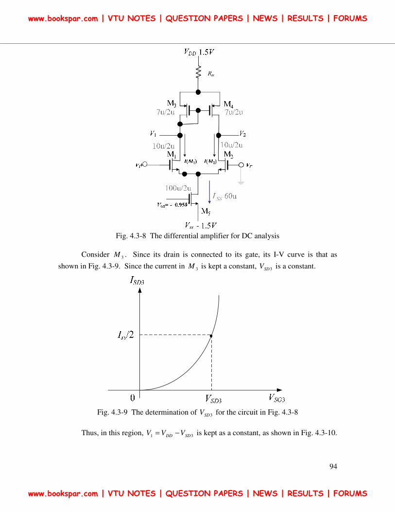
94
Fig. 4.3-8 The differential amplifier for DC analysis
Consider 3M . Since its drain is connected to its gate, its I-V curve is that as
shown in Fig. 4.3-9. Since the current in 3M is kept a constant, 3SDV is a constant.
Fig. 4.3-9 The determination of 3SDV for the circuit in Fig. 4.3-8
Thus, in this region, 31 SDDD VVV −= is kept as a constant, as shown in Fig. 4.3-10.
www.bookspar.com | VTU NOTES | QUESTION PAPERS | NEWS | RESULTS | FORUMS
www.bookspar.com | VTU NOTES | QUESTION PAPERS | NEWS | RESULTS | FORUMS
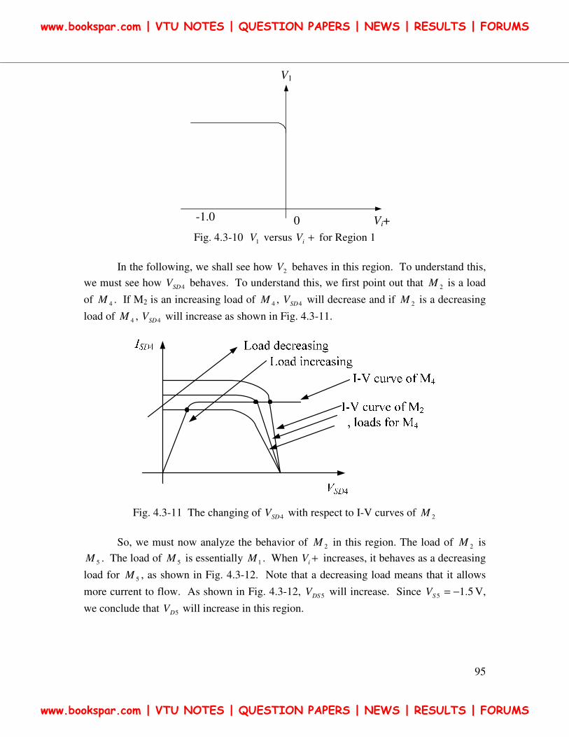
95
Vi+0
V1
-1.0
Fig. 4.3-10 1V versus +iV for Region 1
In the following, we shall see how 2V behaves in this region. To understand this,
we must see how 4SDV behaves. To understand this, we first point out that 2M is a load
of 4M . If M2 is an increasing load of 4M , 4SDV will decrease and if 2M is a decreasing
load of 4M , 4SDV will increase as shown in Fig. 4.3-11.
Fig. 4.3-11 The changing of 4SDV with respect to I-V curves of 2M
So, we must now analyze the behavior of 2M in this region. The load of 2M is
5M . The load of 5M is essentially 1M . When +iV increases, it behaves as a decreasing
load for 5M , as shown in Fig. 4.3-12. Note that a decreasing load means that it allows
more current to flow. As shown in Fig. 4.3-12, 5DSV will increase. Since 5.15 −=SV V,
we conclude that 5DV will increase in this region.
www.bookspar.com | VTU NOTES | QUESTION PAPERS | NEWS | RESULTS | FORUMS
www.bookspar.com | VTU NOTES | QUESTION PAPERS | NEWS | RESULTS | FORUMS
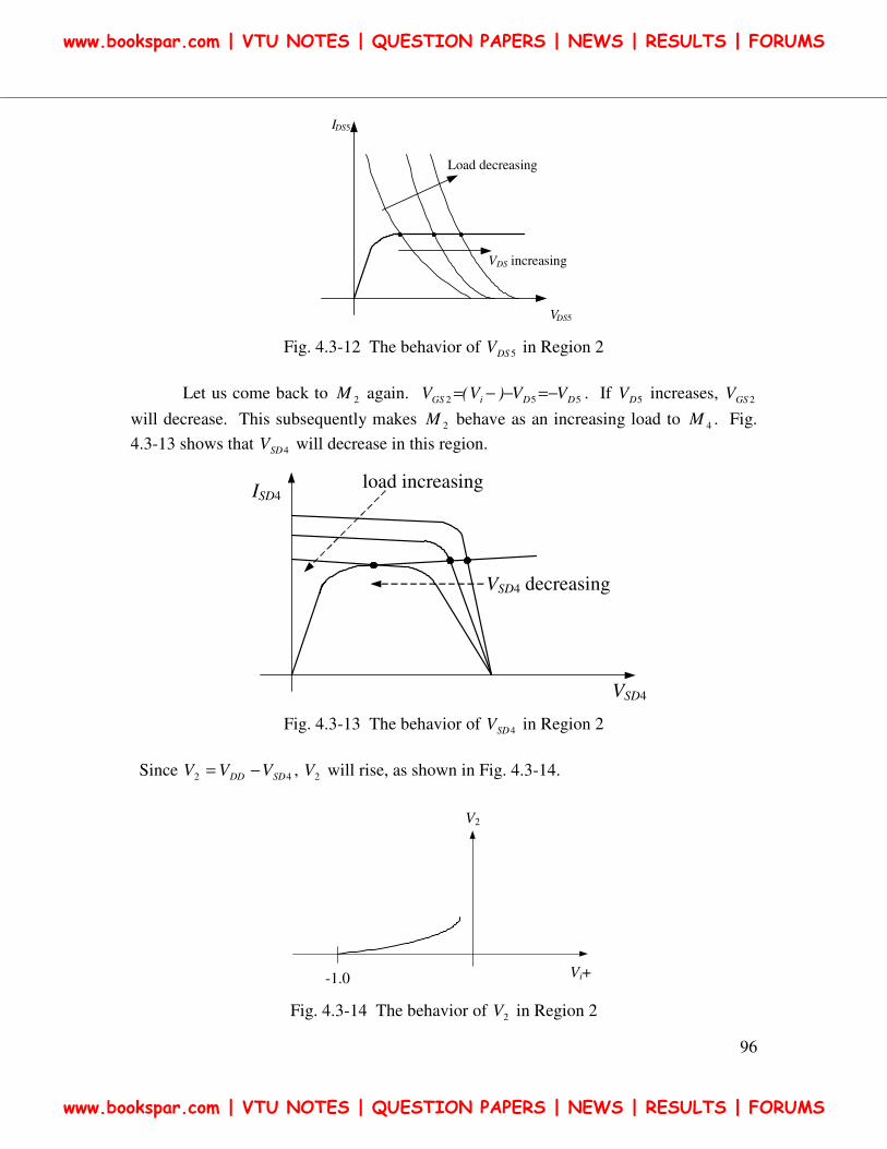
96
IDS5
VDS5
VDS increasing
Load decreasing
Fig. 4.3-12 The behavior of 5DSV in Region 2
Let us come back to 2M again. 552 DDiGS VV)V(V −=−−= . If 5DV increases, 2GSV
will decrease. This subsequently makes 2M behave as an increasing load to 4M . Fig.
4.3-13 shows that 4SDV will decrease in this region.
load increasing
VSD4 decreasing
VSD4
ISD4
Fig. 4.3-13 The behavior of 4SDV in Region 2
Since 42 SDDD VVV −= , 2V will rise, as shown in Fig. 4.3-14.
V2
Vi+-1.0
Fig. 4.3-14 The behavior of 2V in Region 2
www.bookspar.com | VTU NOTES | QUESTION PAPERS | NEWS | RESULTS | FORUMS
www.bookspar.com | VTU NOTES | QUESTION PAPERS | NEWS | RESULTS | FORUMS
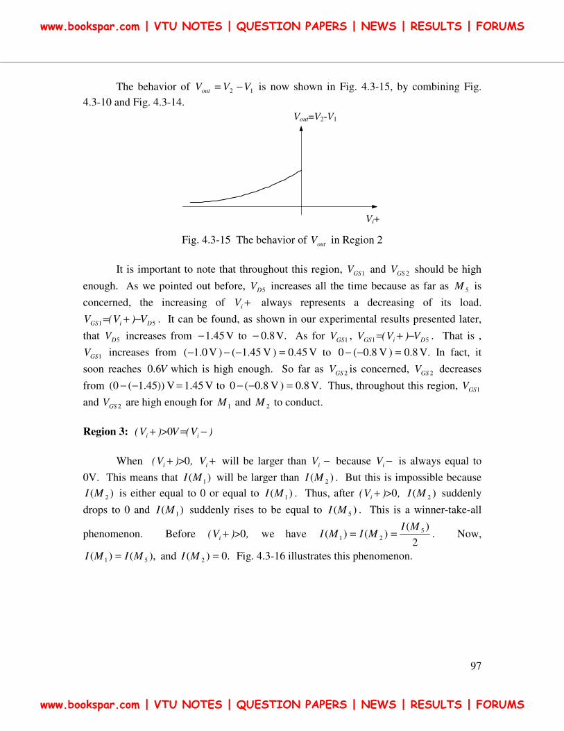
97
The behavior of 12 VVVout −= is now shown in Fig. 4.3-15, by combining Fig.
4.3-10 and Fig. 4.3-14.
Vout=V2-V1
Vi+
Fig. 4.3-15 The behavior of outV in Region 2
It is important to note that throughout this region, 1GSV and 2GSV should be high
enough. As we pointed out before, 5DV increases all the time because as far as 5M is
concerned, the increasing of +iV always represents a decreasing of its load.
51 DiGS V)V(V −+= . It can be found, as shown in our experimental results presented later,
that 5DV increases from 45.1− V to 8.0− V. As for 1GSV , 51 DiGS V)V(V −+= . That is ,
1GSV increases from 0.1(− V 45.1() −− V 45.0) = V to 8.0(0 −− V 8.0) = V. In fact, it
soon reaches V6.0 which is high enough. So far as 2GSV is concerned, 2GSV decreases
from ))45.1(0( −− V 45.1= V to 8.0(0 −− V 8.0) = V. Thus, throughout this region, 1GSV
and 2GSV are high enough for 1M and 2M to conduct.
Region 3: )V(V)V( ii −=>+ 0
When ,)V( i 0>+ +iV will be larger than −iV because −iV is always equal to
0V. This means that )( 1MI will be larger than )( 2MI . But this is impossible because
)( 2MI is either equal to 0 or equal to )( 1MI . Thus, after ,)V( i 0>+ )( 2MI suddenly
drops to 0 and )( 1MI suddenly rises to be equal to )( 5MI . This is a winner-take-all
phenomenon. Before ,)V( i 0>+ we have 2
)()()( 5
21
MIMIMI == . Now,
),()( 51 MIMI = and .0)( 2 =MI Fig. 4.3-16 illustrates this phenomenon.
www.bookspar.com | VTU NOTES | QUESTION PAPERS | NEWS | RESULTS | FORUMS
www.bookspar.com | VTU NOTES | QUESTION PAPERS | NEWS | RESULTS | FORUMS
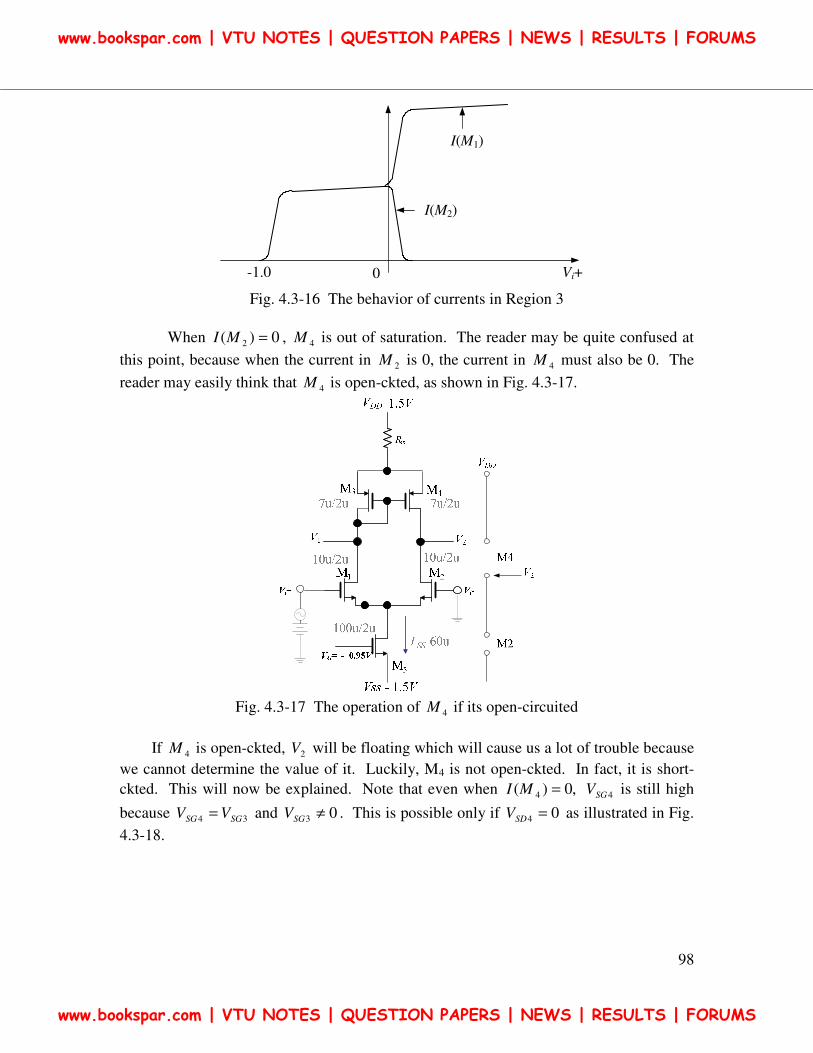
98
I(M1)
I(M2)
-1.0 Vi+0
Fig. 4.3-16 The behavior of currents in Region 3
When 0)( 2 =MI , 4M is out of saturation. The reader may be quite confused at
this point, because when the current in 2M is 0, the current in 4M must also be 0. The
reader may easily think that 4M is open-ckted, as shown in Fig. 4.3-17.
Fig. 4.3-17 The operation of 4M if its open-circuited
If 4M is open-ckted, 2V will be floating which will cause us a lot of trouble because
we cannot determine the value of it. Luckily, M4 is not open-ckted. In fact, it is short-
ckted. This will now be explained. Note that even when ,0)( 4 =MI 4SGV is still high
because 34 SGSG VV = and 03 ≠SGV . This is possible only if 04 =SDV as illustrated in Fig.
4.3-18.
www.bookspar.com | VTU NOTES | QUESTION PAPERS | NEWS | RESULTS | FORUMS
www.bookspar.com | VTU NOTES | QUESTION PAPERS | NEWS | RESULTS | FORUMS
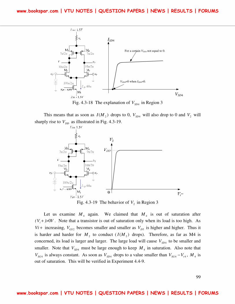
99
ISD4
VSD4
VSD4=0 when ISD4=0.
For a certain VSG4 not equal to 0.
Fig. 4.3-18 The explanation of 4SDV in Region 3
This means that as soon as )( 2MI drops to 0, 4SDV will also drop to 0 and 2V will
sharply rise to DDV as illustrated in Fig. 4.3-19.
Fig. 4.3-19 The behavior of 2V in Region 3
Let us examine 4M again. We claimed that 4M is out of saturation after
V)V( i 0>+ . Note that a transistor is out of saturation only when its load is too high. As
+Vi increasing, 2GSV becomes smaller and smaller as 5DV is higher and higher. Thus it
is harder and harder for 2M to conduct ( )( 2MI drops). Therefore, as far as M4 is
concerned, its load is larger and larger. The large load will cause 4SDV to be smaller and
smaller. Note that 4SDV must be large enough to keep 4M in saturation. Also note that
4SGV is always constant. As soon as 4SDV drops to a value smaller than 44 tSG VV − , 4M is
out of saturation. This will be verified in Experiment 4.4-9.
www.bookspar.com | VTU NOTES | QUESTION PAPERS | NEWS | RESULTS | FORUMS
www.bookspar.com | VTU NOTES | QUESTION PAPERS | NEWS | RESULTS | FORUMS
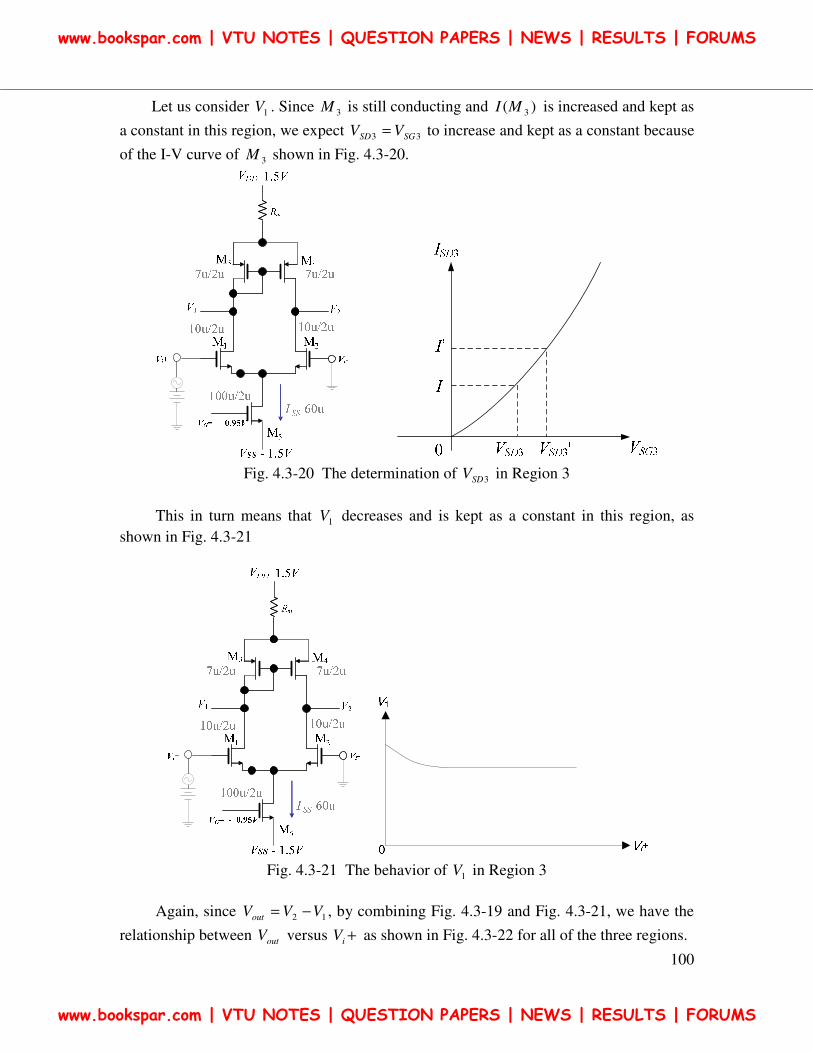
100
Let us consider 1V . Since 3M is still conducting and )( 3MI is increased and kept as
a constant in this region, we expect 33 SGSD VV = to increase and kept as a constant because
of the I-V curve of 3M shown in Fig. 4.3-20.
Fig. 4.3-20 The determination of 3SDV in Region 3
This in turn means that 1V decreases and is kept as a constant in this region, as
shown in Fig. 4.3-21
Fig. 4.3-21 The behavior of 1V in Region 3
Again, since 12 VVVout −= , by combining Fig. 4.3-19 and Fig. 4.3-21, we have the
relationship between outV versus +iV as shown in Fig. 4.3-22 for all of the three regions.
www.bookspar.com | VTU NOTES | QUESTION PAPERS | NEWS | RESULTS | FORUMS
www.bookspar.com | VTU NOTES | QUESTION PAPERS | NEWS | RESULTS | FORUMS
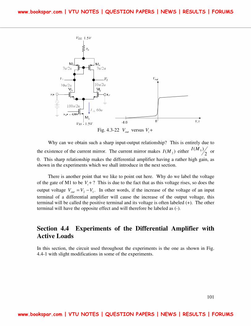
101
Fig. 4.3-22 outV versus +iV
Why can we obtain such a sharp input-output relationship? This is entirely due to
the existence of the current mirror. The current mirror makes )( 2MI either 2
)( 5MI or
0. This sharp relationship makes the differential amplifier having a rather high gain, as
shown in the experiments which we shall introduce in the next section.
There is another point that we like to point out here. Why do we label the voltage
of the gate of M1 to be +iV ? This is due to the fact that as this voltage rises, so does the
output voltage 12 VVVout −= . In other words, if the increase of the voltage of an input
terminal of a differential amplifier will cause the increase of the output voltage, this
terminal will be called the positive terminal and its voltage is often labeled (+). The other
terminal will have the opposite effect and will therefore be labeled as (-).
Section 4.4 Experiments of the Differential Amplifier with
Active Loads
In this section, the circuit used throughout the experiments is the one as shown in Fig.
4.4-1 with slight modifications in some of the experiments.
www.bookspar.com | VTU NOTES | QUESTION PAPERS | NEWS | RESULTS | FORUMS
www.bookspar.com | VTU NOTES | QUESTION PAPERS | NEWS | RESULTS | FORUMS
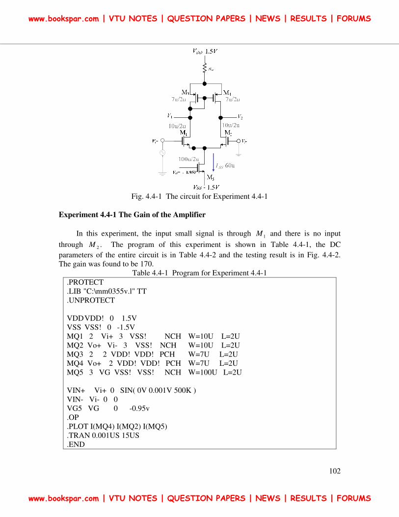
102
Fig. 4.4-1 The circuit for Experiment 4.4-1
Experiment 4.4-1 The Gain of the Amplifier
In this experiment, the input small signal is through 1M and there is no input
through 2M . The program of this experiment is shown in Table 4.4-1, the DC
parameters of the entire circuit is in Table 4.4-2 and the testing result is in Fig. 4.4-2.
The gain was found to be 170.
Table 4.4-1 Program for Experiment 4.4-1
.PROTECT
.LIB "C:\mm0355v.l" TT
.UNPROTECT
VDD VDD! 0 1.5V
VSS VSS! 0 -1.5V
MQ1 2 Vi+ 3 VSS! NCH W=10U L=2U
MQ2 Vo+ Vi- 3 VSS! NCH W=10U L=2U
MQ3 2 2 VDD! VDD! PCH W=7U L=2U
MQ4 Vo+ 2 VDD! VDD! PCH W=7U L=2U
MQ5 3 VG VSS! VSS! NCH W=100U L=2U
VIN+ Vi+ 0 SIN( 0V 0.001V 500K )
VIN- Vi- 0 0
VG5 VG 0 -0.95v
.OP
.PLOT I(MQ4) I(MQ2) I(MQ5)
.TRAN 0.001US 15US
.END
www.bookspar.com | VTU NOTES | QUESTION PAPERS | NEWS | RESULTS | FORUMS
www.bookspar.com | VTU NOTES | QUESTION PAPERS | NEWS | RESULTS | FORUMS
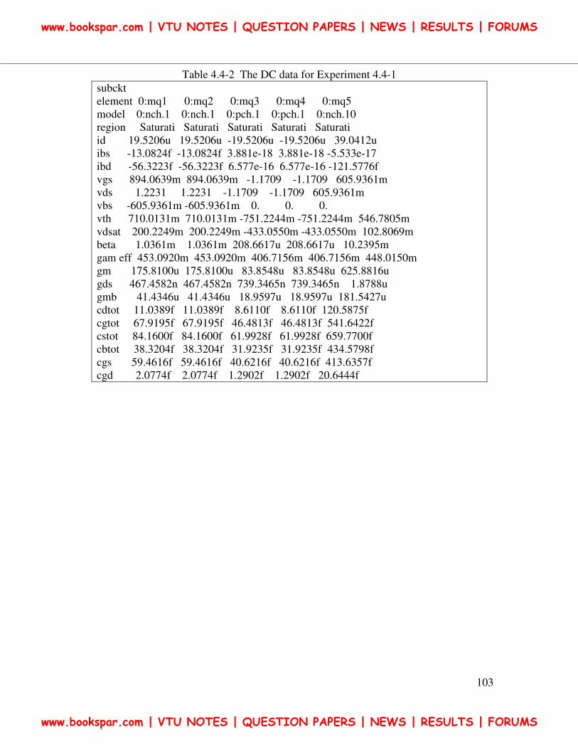
103
Table 4.4-2 The DC data for Experiment 4.4-1
subckt
element 0:mq1 0:mq2 0:mq3 0:mq4 0:mq5
model 0:nch.1 0:nch.1 0:pch.1 0:pch.1 0:nch.10
region Saturati Saturati Saturati Saturati Saturati
id 19.5206u 19.5206u -19.5206u -19.5206u 39.0412u
ibs -13.0824f -13.0824f 3.881e-18 3.881e-18 -5.533e-17
ibd -56.3223f -56.3223f 6.577e-16 6.577e-16 -121.5776f
vgs 894.0639m 894.0639m -1.1709 -1.1709 605.9361m
vds 1.2231 1.2231 -1.1709 -1.1709 605.9361m
vbs -605.9361m -605.9361m 0. 0. 0.
vth 710.0131m 710.0131m -751.2244m -751.2244m 546.7805m
vdsat 200.2249m 200.2249m -433.0550m -433.0550m 102.8069m
beta 1.0361m 1.0361m 208.6617u 208.6617u 10.2395m
gam eff 453.0920m 453.0920m 406.7156m 406.7156m 448.0150m
gm 175.8100u 175.8100u 83.8548u 83.8548u 625.8816u
gds 467.4582n 467.4582n 739.3465n 739.3465n 1.8788u
gmb 41.4346u 41.4346u 18.9597u 18.9597u 181.5427u
cdtot 11.0389f 11.0389f 8.6110f 8.6110f 120.5875f
cgtot 67.9195f 67.9195f 46.4813f 46.4813f 541.6422f
cstot 84.1600f 84.1600f 61.9928f 61.9928f 659.7700f
cbtot 38.3204f 38.3204f 31.9235f 31.9235f 434.5798f
cgs 59.4616f 59.4616f 40.6216f 40.6216f 413.6357f
cgd 2.0774f 2.0774f 1.2902f 1.2902f 20.6444f
www.bookspar.com | VTU NOTES | QUESTION PAPERS | NEWS | RESULTS | FORUMS
www.bookspar.com | VTU NOTES | QUESTION PAPERS | NEWS | RESULTS | FORUMS
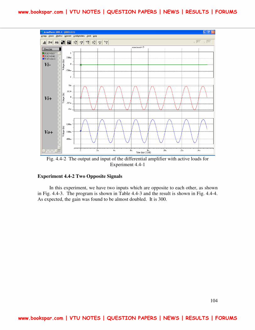
104
Fig. 4.4-2 The output and input of the differential amplifier with active loads for
Experiment 4.4-1
Experiment 4.4-2 Two Opposite Signals
In this experiment, we have two inputs which are opposite to each other, as shown
in Fig. 4.4-3. The program is shown in Table 4.4-3 and the result is shown in Fig. 4.4-4.
As expected, the gain was found to be almost doubled. It is 300.
Vi+
Vi-
Vo+
www.bookspar.com | VTU NOTES | QUESTION PAPERS | NEWS | RESULTS | FORUMS
www.bookspar.com | VTU NOTES | QUESTION PAPERS | NEWS | RESULTS | FORUMS
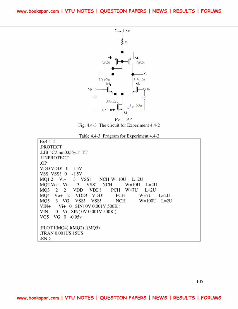
105
Fig. 4.4-3 The circuit for Experiment 4.4-2
Table 4.4-3 Program for Experiment 4.4-2
Ex4.4-2
.PROTECT
.LIB "C:\mm0355v.l" TT
.UNPROTECT
.OP
VDD VDD! 0 1.5V
VSS VSS! 0 -1.5V
MQ1 2 Vi+ 3 VSS! NCH W=10U L=2U
MQ2 Vo+ Vi- 3 VSS! NCH W=10U L=2U
MQ3 2 2 VDD! VDD! PCH W=7U L=2U
MQ4 Vo+ 2 VDD! VDD! PCH W=7U L=2U
MQ5 3 VG VSS! VSS! NCH W=100U L=2U
VIN+ Vi+ 0 SIN( 0V 0.001V 500K )
VIN- 0 Vi- SIN( 0V 0.001V 500K )
VG5 VG 0 -0.95v
.PLOT I(MQ4) I(MQ2) I(MQ5)
.TRAN 0.001US 15US
.END
www.bookspar.com | VTU NOTES | QUESTION PAPERS | NEWS | RESULTS | FORUMS
www.bookspar.com | VTU NOTES | QUESTION PAPERS | NEWS | RESULTS | FORUMS
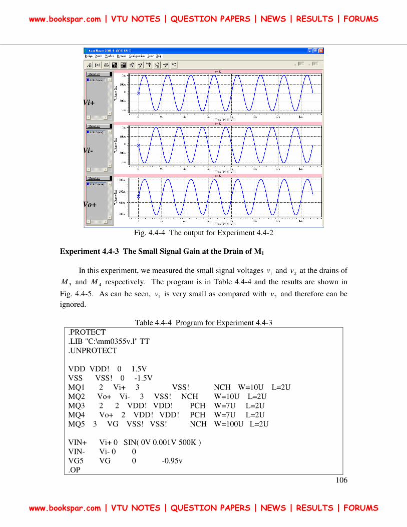
106
Fig. 4.4-4 The output for Experiment 4.4-2
Experiment 4.4-3 The Small Signal Gain at the Drain of M1
In this experiment, we measured the small signal voltages 1v and 2v at the drains of
3M and 4M respectively. The program is in Table 4.4-4 and the results are shown in
Fig. 4.4-5. As can be seen, 1v is very small as compared with 2v and therefore can be
ignored.
Table 4.4-4 Program for Experiment 4.4-3
.PROTECT
.LIB "C:\mm0355v.l" TT
.UNPROTECT
VDD VDD! 0 1.5V
VSS VSS! 0 -1.5V
MQ1 2 Vi+ 3 VSS! NCH W=10U L=2U
MQ2 Vo+ Vi- 3 VSS! NCH W=10U L=2U
MQ3 2 2 VDD! VDD! PCH W=7U L=2U
MQ4 Vo+ 2 VDD! VDD! PCH W=7U L=2U
MQ5 3 VG VSS! VSS! NCH W=100U L=2U
VIN+ Vi+ 0 SIN( 0V 0.001V 500K )
VIN- Vi- 0 0
VG5 VG 0 -0.95v
.OP
Vi+
Vi-
Vo+
www.bookspar.com | VTU NOTES | QUESTION PAPERS | NEWS | RESULTS | FORUMS
www.bookspar.com | VTU NOTES | QUESTION PAPERS | NEWS | RESULTS | FORUMS
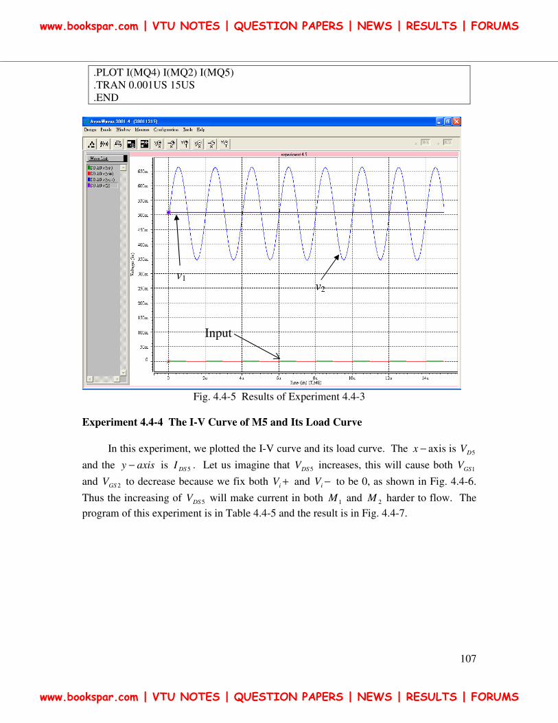
107
.PLOT I(MQ4) I(MQ2) I(MQ5)
.TRAN 0.001US 15US
.END
Fig. 4.4-5 Results of Experiment 4.4-3
Experiment 4.4-4 The I-V Curve of M5 and Its Load Curve
In this experiment, we plotted the I-V curve and its load curve. The −x axis is 5DV
and the axisy − is 5DSI . Let us imagine that 5DSV increases, this will cause both 1GSV
and 2GSV to decrease because we fix both +iV and −iV to be 0, as shown in Fig. 4.4-6.
Thus the increasing of 5DSV will make current in both 1M and 2M harder to flow. The
program of this experiment is in Table 4.4-5 and the result is in Fig. 4.4-7.
Input
v1 v2
www.bookspar.com | VTU NOTES | QUESTION PAPERS | NEWS | RESULTS | FORUMS
www.bookspar.com | VTU NOTES | QUESTION PAPERS | NEWS | RESULTS | FORUMS
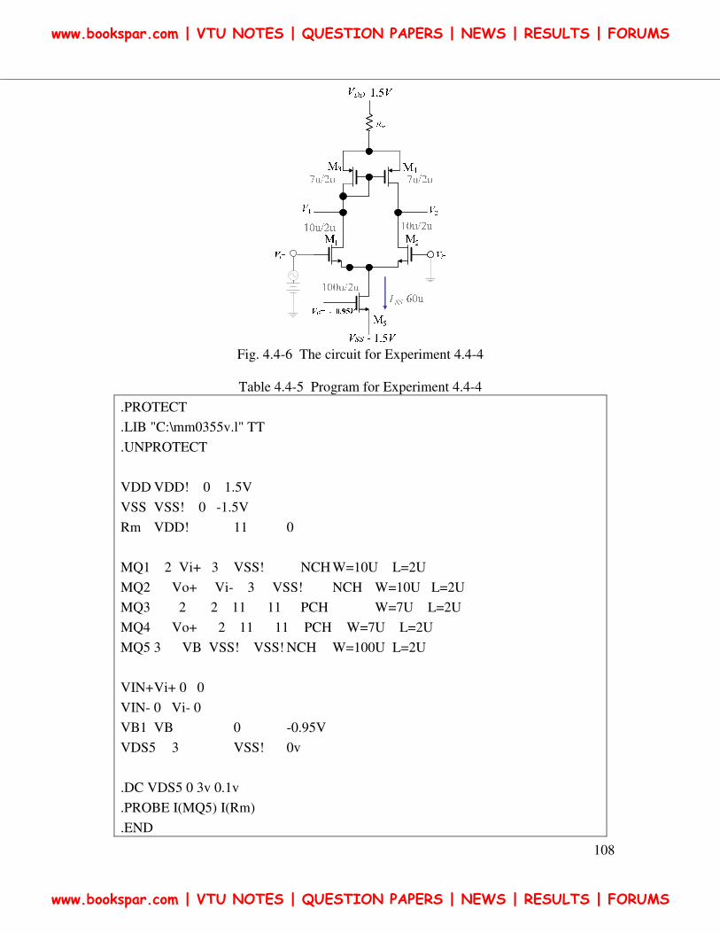
108
Fig. 4.4-6 The circuit for Experiment 4.4-4
Table 4.4-5 Program for Experiment 4.4-4
.PROTECT
.LIB "C:\mm0355v.l" TT
.UNPROTECT
VDD VDD! 0 1.5V
VSS VSS! 0 -1.5V
Rm VDD! 11 0
MQ1 2 Vi+ 3 VSS! NCH W=10U L=2U
MQ2 Vo+ Vi- 3 VSS! NCH W=10U L=2U
MQ3 2 2 11 11 PCH W=7U L=2U
MQ4 Vo+ 2 11 11 PCH W=7U L=2U
MQ5 3 VB VSS! VSS! NCH W=100U L=2U
VIN+ Vi+ 0 0
VIN- 0 Vi- 0
VB1 VB 0 -0.95V
VDS5 3 VSS! 0v
.DC VDS5 0 3v 0.1v
.PROBE I(MQ5) I(Rm)
.END
www.bookspar.com | VTU NOTES | QUESTION PAPERS | NEWS | RESULTS | FORUMS
www.bookspar.com | VTU NOTES | QUESTION PAPERS | NEWS | RESULTS | FORUMS
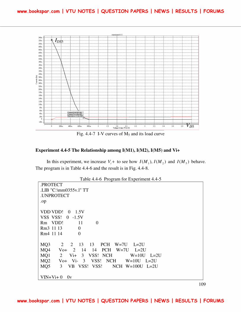
109
Fig. 4.4-7 I-V curves of M5 and its load curve
Experiment 4.4-5 The Relationship among I(M1), I(M2), I(M5) and Vi+
In this experiment, we increase +iV to see how )(),( 21 MIMI and )( 5MI behave.
The program is in Table 4.4-6 and the result is in Fig. 4.4-8.
Table 4.4-6 Program for Experiment 4.4-5
.PROTECT
.LIB "C:\mm0355v.l" TT
.UNPROTECT
.op
VDD VDD! 0 1.5V
VSS VSS! 0 -1.5V
Rm VDD! 11 0
Rm3 11 13 0
Rm4 11 14 0
MQ3 2 2 13 13 PCH W=7U L=2U
MQ4 Vo+ 2 14 14 PCH W=7U L=2U
MQ1 2 Vi+ 3 VSS! NCH W=10U L=2U
MQ2 Vo+ Vi- 3 VSS! NCH W=10U L=2U
MQ5 3 VB VSS! VSS! NCH W=100U L=2U
VIN+ Vi+ 0 0v
IDS5
VD5
www.bookspar.com | VTU NOTES | QUESTION PAPERS | NEWS | RESULTS | FORUMS
www.bookspar.com | VTU NOTES | QUESTION PAPERS | NEWS | RESULTS | FORUMS
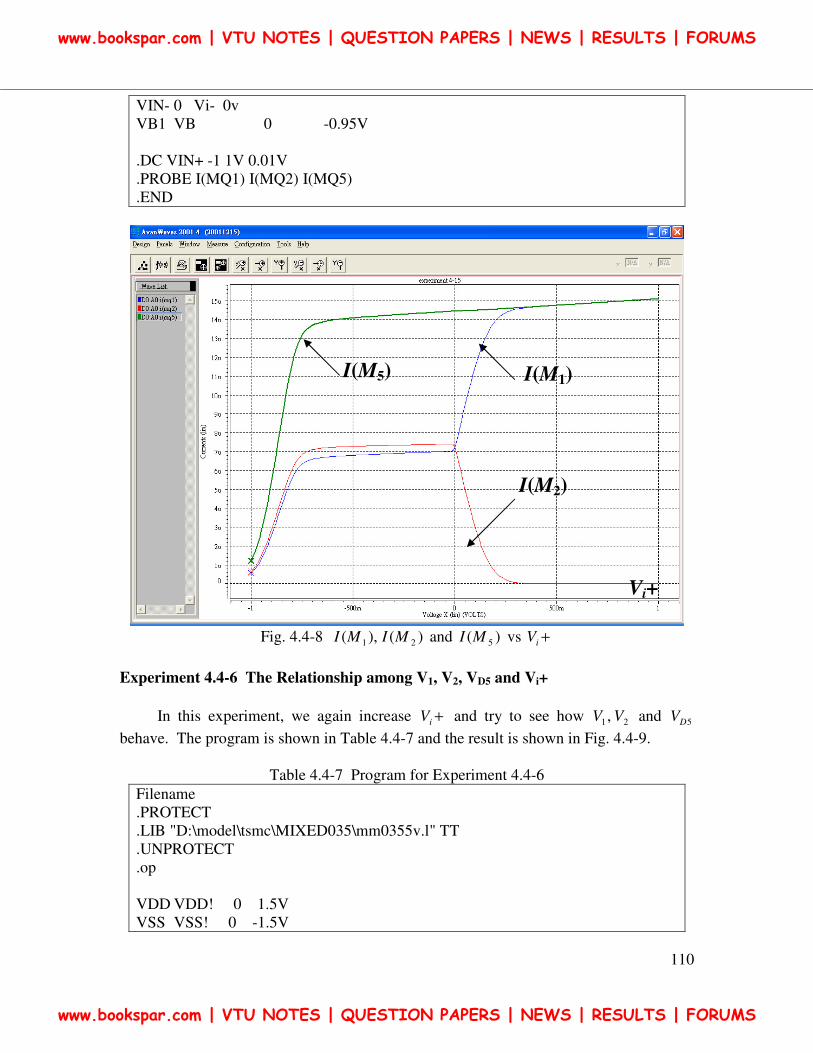
110
VIN- 0 Vi- 0v
VB1 VB 0 -0.95V
.DC VIN+ -1 1V 0.01V
.PROBE I(MQ1) I(MQ2) I(MQ5)
.END
Fig. 4.4-8 )(),( 21 MIMI and )( 5MI vs +iV
Experiment 4.4-6 The Relationship among V1, V2, VD5 and Vi+
In this experiment, we again increase +iV and try to see how 21 , VV and 5DV
behave. The program is shown in Table 4.4-7 and the result is shown in Fig. 4.4-9.
Table 4.4-7 Program for Experiment 4.4-6
Filename
.PROTECT
.LIB "D:\model\tsmc\MIXED035\mm0355v.l" TT
.UNPROTECT
.op
VDD VDD! 0 1.5V
VSS VSS! 0 -1.5V
Vi+
I(M5) I(M1)
I(M2)
www.bookspar.com | VTU NOTES | QUESTION PAPERS | NEWS | RESULTS | FORUMS
www.bookspar.com | VTU NOTES | QUESTION PAPERS | NEWS | RESULTS | FORUMS
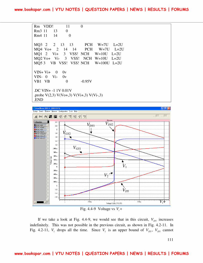
111
Rm VDD! 11 0
Rm3 11 13 0
Rm4 11 14 0
MQ3 2 2 13 13 PCH W=7U L=2U
MQ4 Vo+ 2 14 14 PCH W=7U L=2U
MQ1 2 Vi+ 3 VSS! NCH W=10U L=2U
MQ2 Vo+ Vi- 3 VSS! NCH W=10U L=2U
MQ5 3 VB VSS! VSS! NCH W=100U L=2U
VIN+ Vi+ 0 0v
VIN- 0 Vi- 0v
VB1 VB 0 -0.95V
.DC VIN+ -1 1V 0.01V
.probe V(2,3) V(Vo+,3) V(Vi+,3) V(Vi-,3)
.END
Fig. 4.4-9 Voltage vs +iV
If we take a look at Fig. 4.4-9, we would see that in this circuit, 5DV increases
indefinitely. This was not possible in the previous circuit, as shown in Fig. 4.2-11. In
Fig. 4.2-11, 1V drops all the time. Since 1V is an upper bound of 5DV , 5DV cannot
VDS1 VDS2
VGS2
VGS1
VD5
V1
V2
Vi+
www.bookspar.com | VTU NOTES | QUESTION PAPERS | NEWS | RESULTS | FORUMS
www.bookspar.com | VTU NOTES | QUESTION PAPERS | NEWS | RESULTS | FORUMS
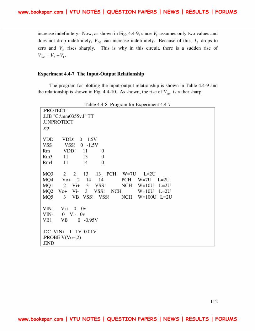
112
increase indefinitely. Now, as shown in Fig. 4.4-9, since 1V assumes only two values and
does not drop indefinitely, 5DV can increase indefinitely. Because of this, 2I drops to
zero and 2V rises sharply. This is why in this circuit, there is a sudden rise of
12 VVVout −= .
Experiment 4.4-7 The Input-Output Relationship
The program for plotting the input-output relationship is shown in Table 4.4-9 and
the relationship is shown in Fig. 4.4-10. As shown, the rise of outV is rather sharp.
Table 4.4-8 Program for Experiment 4.4-7
.PROTECT
.LIB "C:\mm0355v.l" TT
.UNPROTECT
.op
VDD VDD! 0 1.5V
VSS VSS! 0 -1.5V
Rm VDD! 11 0
Rm3 11 13 0
Rm4 11 14 0
MQ3 2 2 13 13 PCH W=7U L=2U
MQ4 Vo+ 2 14 14 PCH W=7U L=2U
MQ1 2 Vi+ 3 VSS! NCH W=10U L=2U
MQ2 Vo+ Vi- 3 VSS! NCH W=10U L=2U
MQ5 3 VB VSS! VSS! NCH W=100U L=2U
VIN+ Vi+ 0 0v
VIN- 0 Vi- 0v
VB1 VB 0 -0.95V
.DC VIN+ -1 1V 0.01V
.PROBE V(Vo+,2)
.END
www.bookspar.com | VTU NOTES | QUESTION PAPERS | NEWS | RESULTS | FORUMS
www.bookspar.com | VTU NOTES | QUESTION PAPERS | NEWS | RESULTS | FORUMS
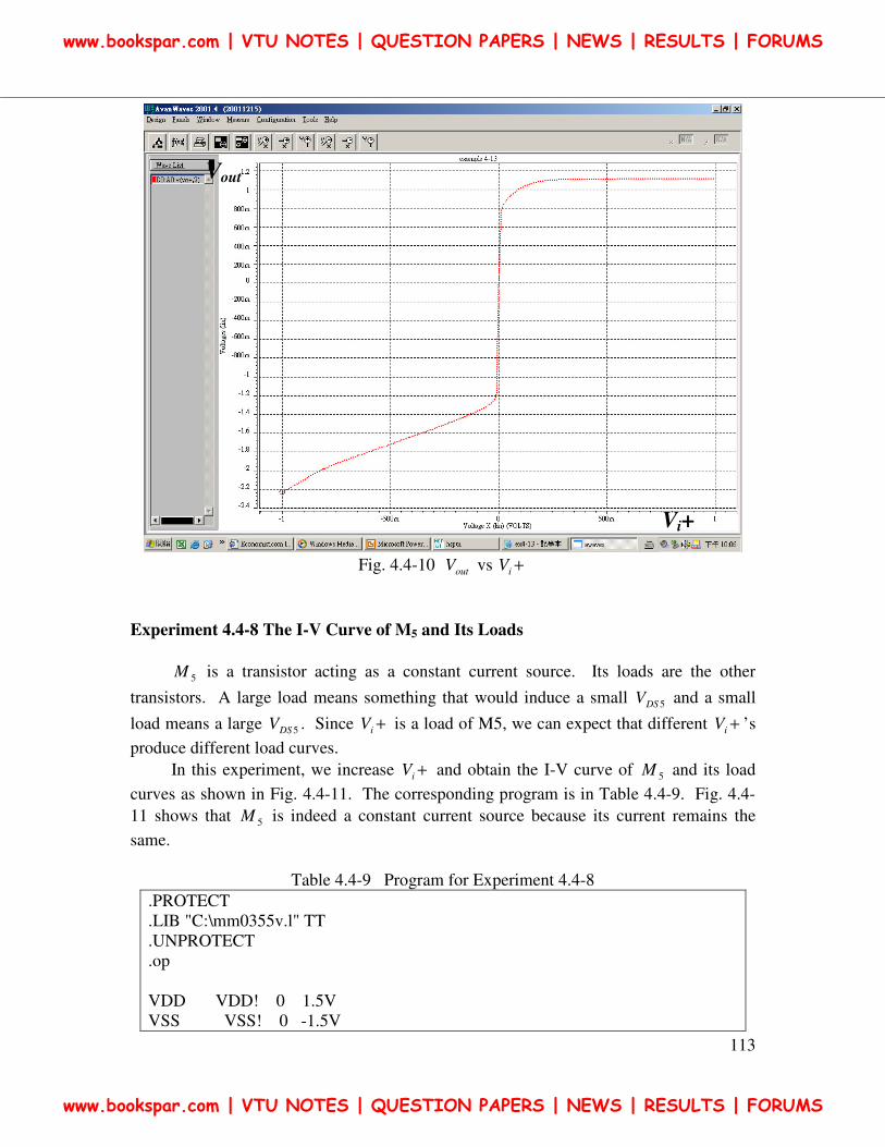
113
Fig. 4.4-10 outV vs +iV
Experiment 4.4-8 The I-V Curve of M5 and Its Loads
5M is a transistor acting as a constant current source. Its loads are the other
transistors. A large load means something that would induce a small 5DSV and a small
load means a large 5DSV . Since +iV is a load of M5, we can expect that different +iV ’s
produce different load curves.
In this experiment, we increase +iV and obtain the I-V curve of 5M and its load
curves as shown in Fig. 4.4-11. The corresponding program is in Table 4.4-9. Fig. 4.4-
11 shows that 5M is indeed a constant current source because its current remains the
same.
Table 4.4-9 Program for Experiment 4.4-8
.PROTECT
.LIB "C:\mm0355v.l" TT
.UNPROTECT
.op
VDD VDD! 0 1.5V
VSS VSS! 0 -1.5V
Vout
Vi+
www.bookspar.com | VTU NOTES | QUESTION PAPERS | NEWS | RESULTS | FORUMS
www.bookspar.com | VTU NOTES | QUESTION PAPERS | NEWS | RESULTS | FORUMS
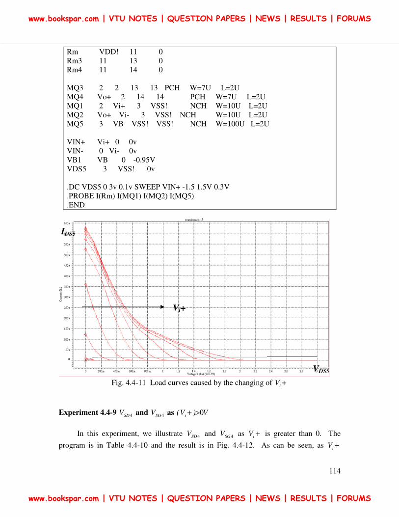
114
Rm VDD! 11 0
Rm3 11 13 0
Rm4 11 14 0
MQ3 2 2 13 13 PCH W=7U L=2U
MQ4 Vo+ 2 14 14 PCH W=7U L=2U
MQ1 2 Vi+ 3 VSS! NCH W=10U L=2U
MQ2 Vo+ Vi- 3 VSS! NCH W=10U L=2U
MQ5 3 VB VSS! VSS! NCH W=100U L=2U
VIN+ Vi+ 0 0v
VIN- 0 Vi- 0v
VB1 VB 0 -0.95V
VDS5 3 VSS! 0v
.DC VDS5 0 3v 0.1v SWEEP VIN+ -1.5 1.5V 0.3V
.PROBE I(Rm) I(MQ1) I(MQ2) I(MQ5)
.END
Fig. 4.4-11 Load curves caused by the changing of +iV
Experiment 4.4-9 4SDV and 4SGV as V)V( i 0>+
In this experiment, we illustrate 4SDV and 4SGV as +iV is greater than 0. The
program is in Table 4.4-10 and the result is in Fig. 4.4-12. As can be seen, as +iV
VDS5
IDS5
Vi+
increasing
www.bookspar.com | VTU NOTES | QUESTION PAPERS | NEWS | RESULTS | FORUMS
www.bookspar.com | VTU NOTES | QUESTION PAPERS | NEWS | RESULTS | FORUMS
115
increases, 4SGV remains roughly as a constant. But 4SDV drops sharply. This drop causes
4M to be out of saturation.
Table 4.4-10 Program for Experiment 4.4-9
.PROTECT
.OPTION POST
.LIB "C:\mm0355v.l" TT
.UNPROTECT
.op
VDD VDD! 0 1.5V
VSS VSS! 0 -1.5V
Rm VDD! 11 0
MQ1 2 Vi+ 3 VSS! NCH W=10U L=2U
MQ2 Vo+ Vi- 3 VSS! NCH W=10U L=2U
MQ3 2 2 11 11 PCH W=7U L=2U
MQ4 Vo+ 2 11 11 PCH W=7U L=2U
MQ5 3 VB VSS! VSS! NCH W=100U L=2U
VIN+ Vi+ 0 0v
VIN- Vi- 0 0v
VB1 VB 0 -0.95V
.DC VIN+ -1v 1v 0.1v
.PROBE V(11,Vo+) V(11,2)
.END
www.bookspar.com | VTU NOTES | QUESTION PAPERS | NEWS | RESULTS | FORUMS
www.bookspar.com | VTU NOTES | QUESTION PAPERS | NEWS | RESULTS | FORUMS
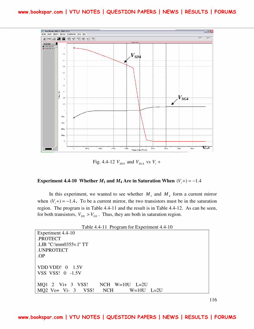
116
Fig. 4.4-12 4SDV and 4SGV vs +iV
Experiment 4.4-10 Whether M1 and M4 Are in Saturation When 4.1)( −=+iV
In this experiment, we wanted to see whether 1M and 4M form a current mirror
when 4.1)( −=+iV . To be a current mirror, the two transistors must be in the saturation
region. The program is in Table 4.4-11 and the result is in Table 4.4-12. As can be seen,
for both transistors, GSDS VV > . Thus, they are both in saturation region.
Table 4.4-11 Program for Experiment 4.4-10
Experiment 4.4-10
.PROTECT
.LIB "C:\mm0355v.l" TT
.UNPROTECT
.OP
VDD VDD! 0 1.5V
VSS VSS! 0 -1.5V
MQ1 2 Vi+ 3 VSS! NCH W=10U L=2U
MQ2 Vo+ Vi- 3 VSS! NCH W=10U L=2U
VSD4
VSG4
Vi+
www.bookspar.com | VTU NOTES | QUESTION PAPERS | NEWS | RESULTS | FORUMS
www.bookspar.com | VTU NOTES | QUESTION PAPERS | NEWS | RESULTS | FORUMS
117
MQ3 2 2 VDD! VDD! PCH W=7U L=2U
MQ4 Vo+ 2 VDD! VDD! PCH W=7U L=2U
MQ5 3 VG VSS! VSS! NCH W=100U L=2U
VIN+ Vi+ 0 -1.4v
VIN- Vi- 0 0
VG5 VG 0 -0.95v
.END
Table 4.4-12 Results of Experiment 4.4-10
subckt
element 0:mq1 0:mq2 0:mq3 0:mq4 0:mq5
model 0:nch.1 0:nch.1 0:pch.1 0:pch.1 0:nch.10
region Cutoff Linear Cutoff Cutoff Linear
id 14.0076p 32.1686p -18.8189p -26.1673p 48.8709p
ibs -7.486e-20 -7.488e-20 3.813e-24 5.816e-24 -6.928e-23
ibd -31.9597f -9.416e-20 6.559e-16 1.3764f -6.954e-19
vgs 99.9999m 1.5000 -304.9841m -304.9841m 550.0000m
vds 2.6950 38.0424n -304.9841m -3.0000 146.9613n
vbs -146.9613n -146.9613n 0. 0. 0.
vth 548.0127m 551.7676m -754.4888m -744.2205m 547.7465m
vdsat 42.2588m 780.6222m -47.8223m -47.8231m 73.1017m
beta 1.0813m 969.9030u 222.2774u 222.9576u 10.2582m
gam eff 466.9524m 466.9524m 406.7153m 406.7153m 448.0154m
gm 413.7615p 27.8973p 523.8515p 726.7963p 713.4532p
gds 2.5195p 849.8482u 2.9968p 2.9888p 332.6087u
gmb 141.2239p 10.3957p 146.0971p 201.5168p 211.4849p
cdtot 10.4477f 93.2072f 10.8270f 6.5920f 171.7111f
cgtot 28.6226f 95.2831f 17.5353f 17.5353f 263.4718f
cstot 14.2785f 98.2692f 12.2133f 12.2133f 173.8695f
cbtot 45.0390f 50.0726f 35.4150f 31.1800f 426.4893f
cgs 2.0774f 47.2824f 1.2902f 1.2902f 40.4417f
cgd 2.0774f 47.2824f 1.2902f 1.2902f 40.4407f
Section 4.5 The Small Signal Analysis of the Differential
Amplifier with Active Loads
Let us redraw the differential amplifier circuit in Fig. 4.5-1.
www.bookspar.com | VTU NOTES | QUESTION PAPERS | NEWS | RESULTS | FORUMS
www.bookspar.com | VTU NOTES | QUESTION PAPERS | NEWS | RESULTS | FORUMS
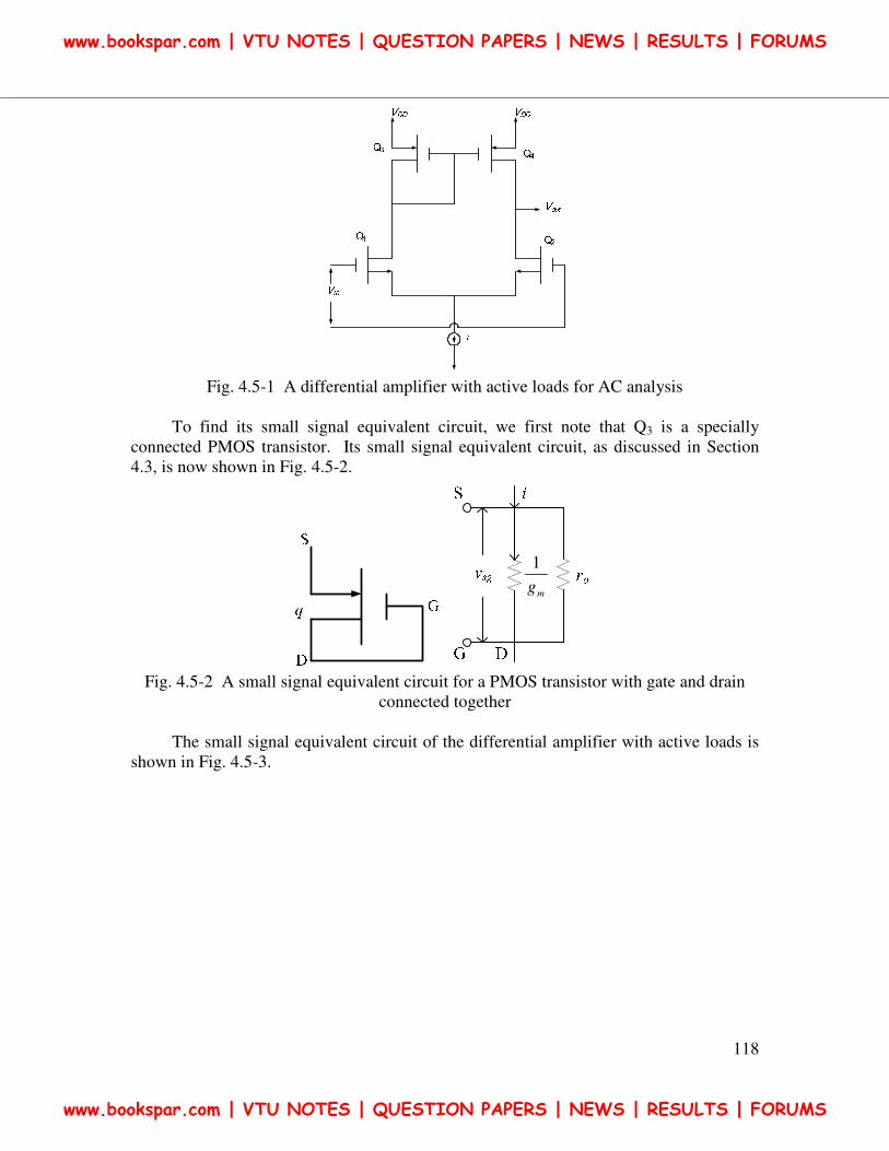
118
Vin I
VDDVDDVoutQ4 Q2Q1
Q3
Fig. 4.5-1 A differential amplifier with active loads for AC analysis
To find its small signal equivalent circuit, we first note that Q3 is a specially
connected PMOS transistor. Its small signal equivalent circuit, as discussed in Section
4.3, is now shown in Fig. 4.5-2.
mg
1
Fig. 4.5-2 A small signal equivalent circuit for a PMOS transistor with gate and drain
connected together
The small signal equivalent circuit of the differential amplifier with active loads is
shown in Fig. 4.5-3.
www.bookspar.com | VTU NOTES | QUESTION PAPERS | NEWS | RESULTS | FORUMS
www.bookspar.com | VTU NOTES | QUESTION PAPERS | NEWS | RESULTS | FORUMS
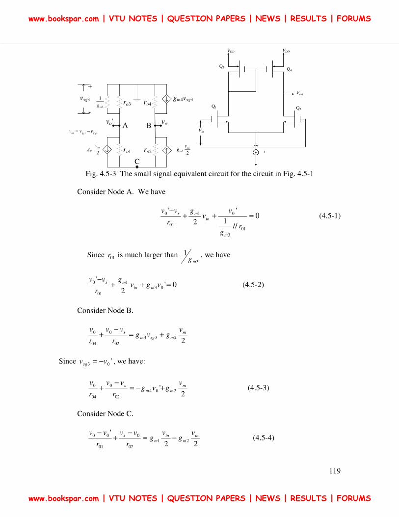
119
ro2ro1
ro4ro3
A B
C
vovo'
3
1
mg
vsg3
+
-
sgsgin vvv21
−=
21
in
m
vg
22
inm
vg
gm4vsg3
Vin
I
VDDVDD
Vout
Q4
Q2Q1
Q3
Fig. 4.5-3 The small signal equivalent circuit for the circuit in Fig. 4.5-1
Consider Node A. We have
0
//1
'
2
'
01
3
01
01
0 =++−
rg
vv
g
r
vv
m
in
ms (4.5-1)
Since 01r is much larger than 3
1mg
, we have
0'2
'03
1
01
0 =++−
vgvg
r
vvmin
ms (4.5-2)
Consider Node B.
2
234
02
0
04
0 m
msgm
s vgvg
r
vv
r
v+=
−+
Since '03 vvsg −= , we have:
2
' 204
02
0
04
0 m
mm
s vgvg
r
vv
r
v+−=
−+ (4.5-3)
Consider Node C.
22
'21
02
0
01
00 in
m
in
m
s vg
vg
r
vv
r
vv−=
−+
− (4.5-4)
www.bookspar.com | VTU NOTES | QUESTION PAPERS | NEWS | RESULTS | FORUMS
www.bookspar.com | VTU NOTES | QUESTION PAPERS | NEWS | RESULTS | FORUMS
120
To simplify the discussion, we assume that mmmmm ggggg ==== 4321 and
004030201 rrrrr ==== . Thus, we have
0'2
'0
0
0 =++−
vgvg
r
vvmin
ms (4.5-5)
02
'0
0
0
0
0 =−+−
+ m
mm
s vgvg
r
vv
r
v (4.5-6)
0'
0
0
0
00 =−
+−
r
vv
r
vv s (4.5-7)
(4.5-5)+(4.5-6)+(4.5-7):
0'20
0
0 =+r
vvgm
0
0
02
'rg
vv
m
= (4.5-8)
2
'00 vvvs
+=
)2
(2
1
0
0
0rg
vvv
m
s −= (4.5-9)
Substituting (4.5-8) and (4.5-9) into (4.5-5), we have:
02
)2
(42
)2
(1
0
0
2
0
0
0
0
0
0
0
=+−
++−− in
m
m
m
mm
vg
rg
vg
rg
v
r
v
rg
v
r (4.5-10)
in
m
m
vg
rrrgv
2)
2
1
2
1
4
1(
00
2
0
0 =++ (4.5-11)
in
m
m
m vg
rg
rgv
2)
4
41(
2
0
0
0 =+
(4.5-12)
Since 14 0 >>rg m , we have
www.bookspar.com | VTU NOTES | QUESTION PAPERS | NEWS | RESULTS | FORUMS
www.bookspar.com | VTU NOTES | QUESTION PAPERS | NEWS | RESULTS | FORUMS
121
Gain 0
0
2
1rg
v
vm
in
== (4.5-13)
Thus the gain is quite large.
Let us find '0v . Using Equations (4.5-13) and (4.5-8), we have:
inin
m
m
om
vvrg
rg
rg
vv
4
1
4
1
2'
0
00
0 ==−= (4.5-14)
Note that inv is very small. The above equation confirms our statement made
before that the small signal voltage at the drain of 3M can be ignored.
Cascode Current Mirror
www.bookspar.com | VTU NOTES | QUESTION PAPERS | NEWS | RESULTS | FORUMS
www.bookspar.com | VTU NOTES | QUESTION PAPERS | NEWS | RESULTS | FORUMS
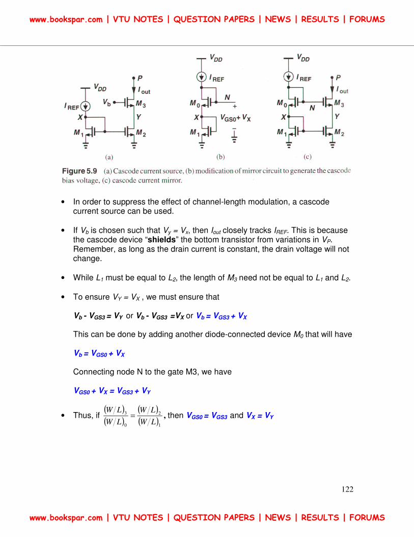
122
• In order to suppress the effect of channel-length modulation, a cascode
current source can be used. • If Vb is chosen such that Vy = Vx, then Iout closely tracks IREF. This is because
the cascode device “shields” the bottom transistor from variations in VP. Remember, as long as the drain current is constant, the drain voltage will not change.
• While L1 must be equal to L2, the length of M3 need not be equal to L1 and L2.
• To ensure VY = VX , we must ensure that
Vb - VGS3 = VY or Vb - VGS3 =VX or Vb = VGS3 + VX This can be done by adding another diode-connected device M0 that will have Vb = VGS0 + VX Connecting node N to the gate M3, we have VGS0 + VX = VGS3 + VY
• Thus, if ( )
( )
( )
( )1
2
0
3
LW
LW
LW
LW= , then VGS0 = VGS3 and VX = VY
www.bookspar.com | VTU NOTES | QUESTION PAPERS | NEWS | RESULTS | FORUMS
www.bookspar.com | VTU NOTES | QUESTION PAPERS | NEWS | RESULTS | FORUMS
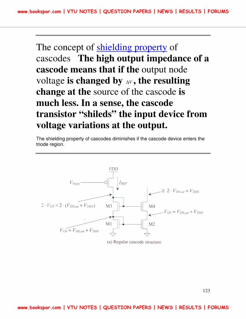
123
The concept of shielding property of
cascodes The high output impedance of a
cascode means that if the output node
voltage is changed by V∆ , the resulting
change at the source of the cascode is
much less. In a sense, the cascode
transistor “shileds” the input device from
voltage variations at the output. The shielding property of cascodes diminishes if the cascode device enters the triode region.
www.bookspar.com | VTU NOTES | QUESTION PAPERS | NEWS | RESULTS | FORUMS
www.bookspar.com | VTU NOTES | QUESTION PAPERS | NEWS | RESULTS | FORUMS
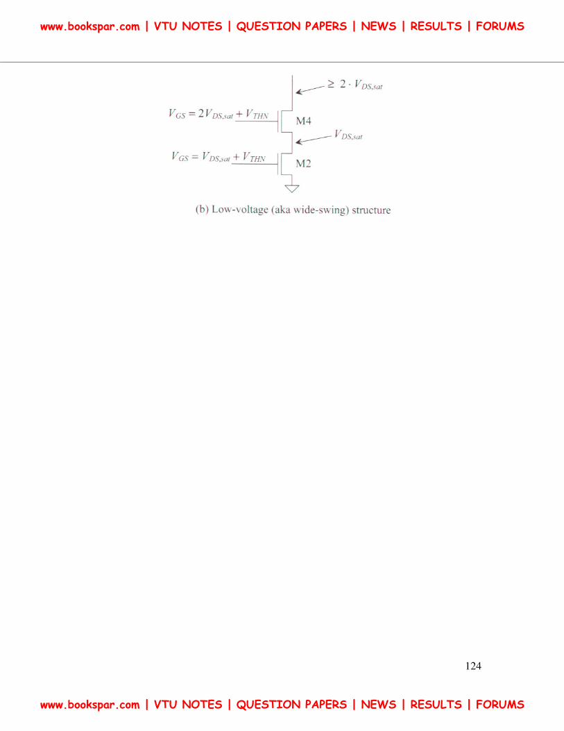
124
www.bookspar.com | VTU NOTES | QUESTION PAPERS | NEWS | RESULTS | FORUMS
www.bookspar.com | VTU NOTES | QUESTION PAPERS | NEWS | RESULTS | FORUMS
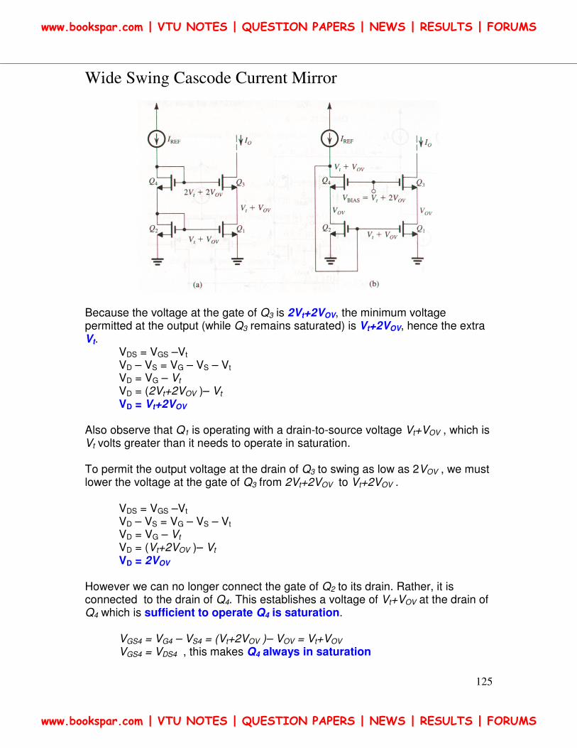
125
Wide Swing Cascode Current Mirror
Because the voltage at the gate of Q3 is 2Vt+2VOV, the minimum voltage permitted at the output (while Q3 remains saturated) is Vt+2VOV, hence the extra Vt.
VDS = VGS –Vt VD – VS = VG – VS – Vt VD = VG – Vt VD = (2Vt+2VOV )– Vt VD = Vt+2VOV
Also observe that Q1 is operating with a drain-to-source voltage Vt+VOV , which is Vt volts greater than it needs to operate in saturation. To permit the output voltage at the drain of Q3 to swing as low as 2VOV , we must lower the voltage at the gate of Q3 from 2Vt+2VOV to Vt+2VOV .
VDS = VGS –Vt VD – VS = VG – VS – Vt VD = VG – Vt VD = (Vt+2VOV )– Vt VD = 2VOV
However we can no longer connect the gate of Q2 to its drain. Rather, it is connected to the drain of Q4. This establishes a voltage of Vt+VOV at the drain of Q4 which is sufficient to operate Q4 is saturation.
VGS4 = VG4 – VS4 = (Vt+2VOV )– VOV = Vt+VOV VGS4 = VDS4 , this makes Q4 always in saturation
www.bookspar.com | VTU NOTES | QUESTION PAPERS | NEWS | RESULTS | FORUMS
www.bookspar.com | VTU NOTES | QUESTION PAPERS | NEWS | RESULTS | FORUMS
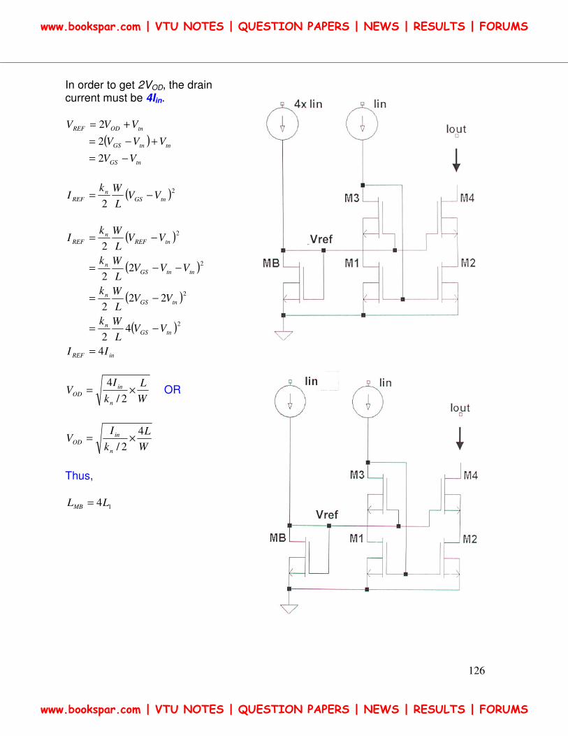
126
In order to get 2VOD, the drain current must be 4Iin.
( )
tnGS
tntnGS
tnODREF
VV
VVV
VVV
−=
+−=
+=
2
2
2
( )2
2tnGS
n
REF VVL
WkI −=
( )
( )
( )
( )
inREF
tnGS
n
tnGS
n
tntnGS
n
tnREF
n
REF
II
VVL
Wk
VVL
Wk
VVVL
Wk
VVL
WkI
4
42
222
22
2
2
2
2
2
=
−=
−=
−−=
−=
W
L
k
IV
n
in
OD ×=2/
4 OR
W
L
k
IV
n
in
OD
4
2/×=
Thus,
14LLMB =
www.bookspar.com | VTU NOTES | QUESTION PAPERS | NEWS | RESULTS | FORUMS
www.bookspar.com | VTU NOTES | QUESTION PAPERS | NEWS | RESULTS | FORUMS
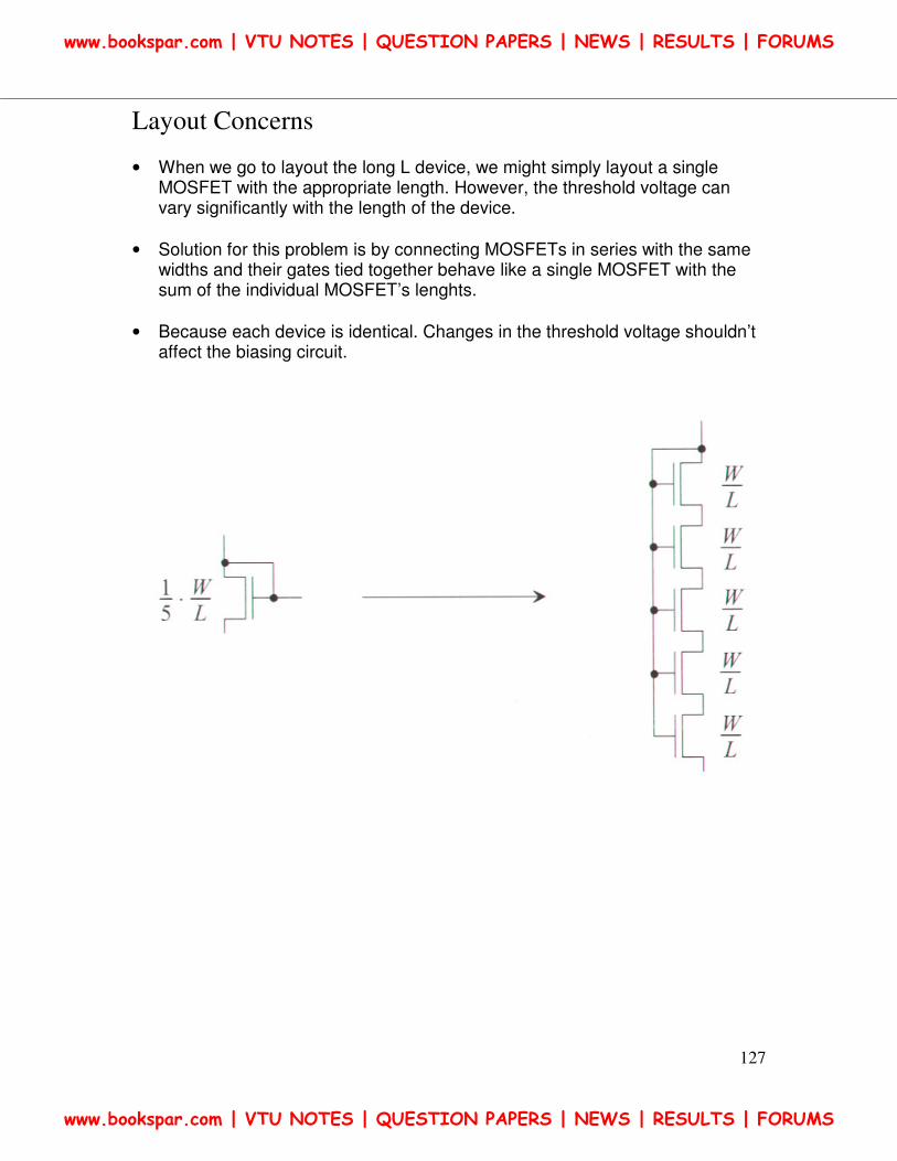
127
Layout Concerns • When we go to layout the long L device, we might simply layout a single
MOSFET with the appropriate length. However, the threshold voltage can vary significantly with the length of the device.
• Solution for this problem is by connecting MOSFETs in series with the same
widths and their gates tied together behave like a single MOSFET with the sum of the individual MOSFET’s lenghts.
• Because each device is identical. Changes in the threshold voltage shouldn’t
affect the biasing circuit.
www.bookspar.com | VTU NOTES | QUESTION PAPERS | NEWS | RESULTS | FORUMS
www.bookspar.com | VTU NOTES | QUESTION PAPERS | NEWS | RESULTS | FORUMS