Embed Size (px)
Citation preview
AN135
Rev 0.8 | Page 1/40
www.hoperf.com
1. 概要
本文的目的是对用外部 MCU 控制 CMT2119A 及 CMT2219A 的方法及示例代码进行简要说明。
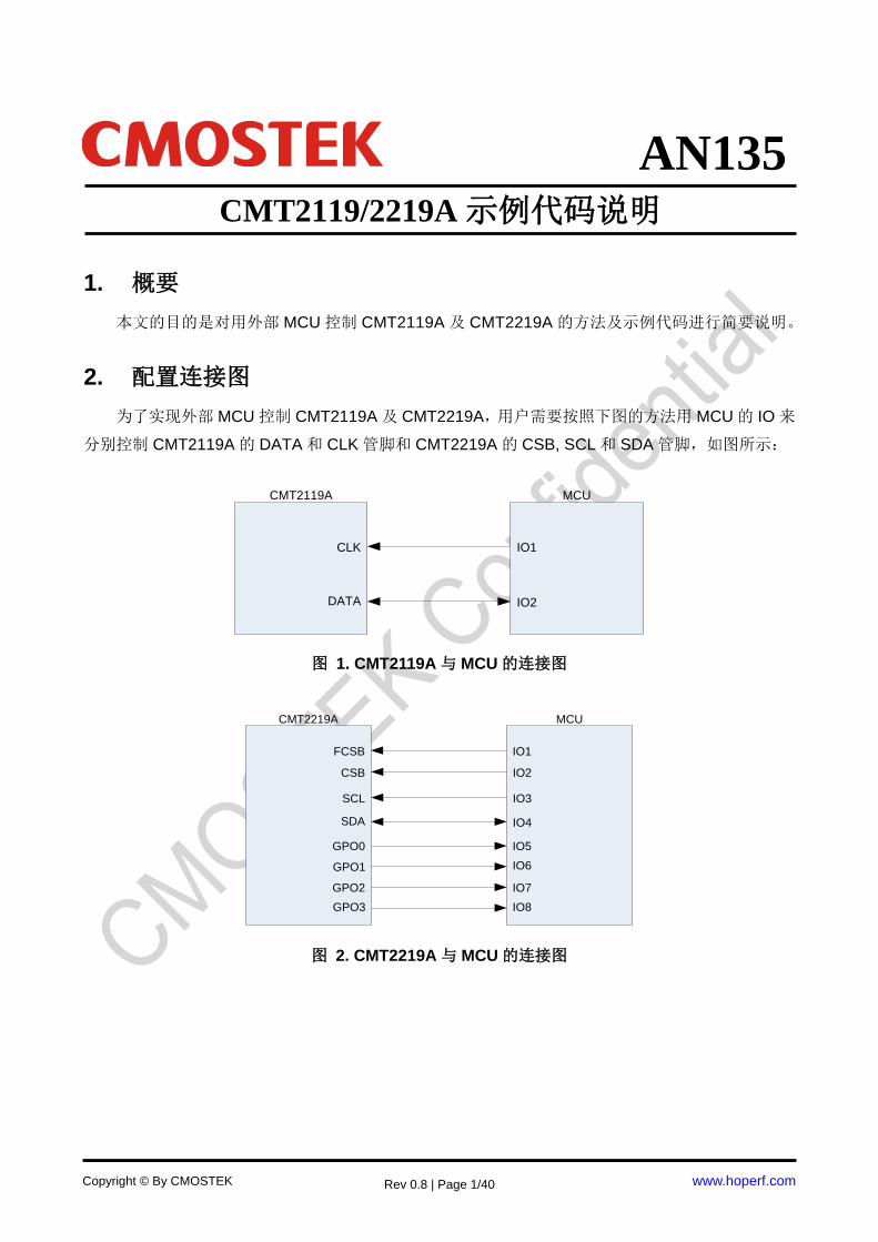
2. 配置连接图
为了实现外部 MCU 控制 CMT2119A 及 CMT2219A,用户需要按照下图的方法用 MCU 的 IO 来
分别控制 CMT2119A 的 DATA 和 CLK 管脚和 CMT2219A 的 CSB, SCL 和 SDA 管脚,如图所示:
DATA
CLK IO1
IO2
CMT2119A MCU
图 1. CMT2119A 与 MCU 的连接图
SDA
SCL IO3
IO4
CMT2219A MCU
CSB IO2
FCSB IO1
IO5
IO6
IO7
IO8
GPO0
GPO1
GPO2
GPO3
图 2. CMT2219A 与 MCU 的连接图
Copyright © By CMOSTEK
AN135 CMT2119/2219A 示例代码说明
AN135
Rev 0.8 | Page 2/40
www.hoperf.com
3. CMT2119A 示例代码说明
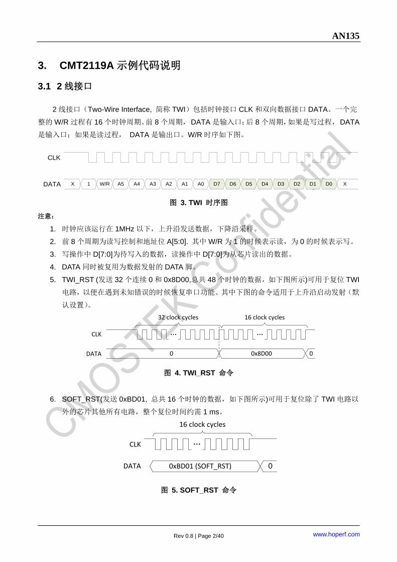
3.1 2 线接口
2 线接口(Two-Wire Interface, 简称 TWI)包括时钟接口 CLK 和双向数据接口 DATA。一个完
整的 W/R 过程有 16 个时钟周期。前 8 个周期, DATA 是输入口;后 8 个周期,如果是写过程, DATA
是输入口;如果是读过程, DATA 是输出口。W/R 时序如下图。
CLK
DATA W/R A51 A4 A2 A1A3 A0 D6 D5D7 D4 D2 D1D3 D0 X X
图 3. TWI 时序图
注意:
1. 时钟应该运行在 1MHz 以下,上升沿发送数据,下降沿采样。
2. 前 8 个周期为读写控制和地址位 A[5:0]. 其中 W/R 为 1 的时候表示读,为 0 的时候表示写。
3. 写操作中 D[7:0]为待写入的数据,读操作中 D[7:0]为从芯片读出的数据。
4. DATA 同时被复用为数据发射的 DATA 脚。
5. TWI_RST (发送 32 个连续 0 和 0x8D00,总共 48 个时钟的数据,如下图所示)可用于复位 TWI
电路,以便在遇到未知错误的时候恢复串口功能。其中下图的命令适用于上升沿启动发射(默
认设置)。
CLK
32 clock cycles
… …
16 clock cycles
DATA 0x8D000 0
图 4. TWI_RST 命令
6. SOFT_RST(发送 0xBD01, 总共 16 个时钟的数据,如下图所示)可用于复位除了 TWI 电路以
外的芯片其他所有电路,整个复位时间约需 1 ms。
DATA
CLK
16 clock cycles
0xBD01 (SOFT_RST)
…
0
图 5. SOFT_RST 命令
AN135
Rev 0.8 | Page 3/40
www.hoperf.com
7. 方便起见,本文用 TWI_RDREG 表示 TWI 读操作,用 TWI_WRREG 表示 TWI 写操作。
a) TWI_RDREG(XX, YY)为发送 8b’ 11xx xxxx 读出 yyyy yyyy,其中 xx xxxx 为待读地址,
范围 0x00 到 0x3F; yyyy yyyy 为读出值,范围为 0x00 到 0xFF。
b) TWI_WRREG(XX, ZZ)为发送 16’ 10xx xxxx zzzz zzzz,其中例如 xx xxxx 为待写地址,范
围 0x00 到 0x3F; zzzz zzzz 为待写值,范围为 0x00 到 0xFF。
c) 例如:
i. 从地址 0x01 读取数据表示为 TWI_RDREG(0x1, DAT), 其中 DAT 表示从地址 0x1
读出的数据。
ii. 对地址 0x2 写入数据 0xAA 表示为 TWI_WRREG(0x2, 0xAA)。
iii. SOFT_RST 可表示为 TWI_WRREG(0x3D, 0x01)。
8. DATA 是一个双向数据口,在读操作的后 8 个周期会被切换为输出口。为了避免潜在的电平冲
突,当 DATA 切换为输出口的时候,主控(Master)相应的驱动端口要及时切换为输入口。
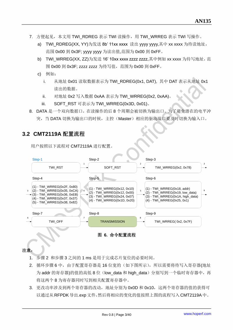
3.2 CMT2119A 配置流程
用户按照以下流程对 CMT2119A 进行配置。
TWI_RST SOFT_RST TWI_WRREG(0x2, 0x78)
(1) - TWI_WRREG(0x2F, 0x80)
(2) - TWI_WRREG(0x35, 0xCA)
(3) - TWI_WRREG(0x36, 0xEB)
(4) - TWI_WRREG(0x37, 0x37)
(5) - TWI_WRREG(0x38, 0x82)
(1) - TWI_WRREG(0x12, 0x10)
(2) - TWI_WRREG(0x12, 0x00)
(3) - TWI_WRREG(0x24, 0x07)
(4) - TWI_WRREG(0x1D, 0x20)
(1) - TWI_WRREG(0x18, addr)
(2) - TWI_WRREG(0x19, low_data)
(3) - TWI_WRREG(0x1A, high_data)
(4) - TWI_WRREG(0x25, 0x1)
TWI_OFF TRANSMISSION TWI_WRREG( 0x2, 0x7F)
1 2 3
3 4 5 6
6 7 8
Step-1 Step-2 Step-3
Step-4 Step-5
Step-7 Step-8 Step-9
Step-6
图 6. 命令配置流程
注意:
1. 步骤 2 和步骤 3 之间的 1 ms 是用于完成芯片复位的必要时间。
2. 循环步骤 6 中,由于配置寄存器是 16 位宽的(如下图所示),所以需要将待写入寄存器(地址
为 addr 的寄存器)的值的高低 8 位(low_data 和 high_data)分别写到一个临时寄存器中,再
将这两个 8 为寄存器同时写到相关配置寄存器中。
3. 更改功率涉及到两个寄存器的改动,地址分别为 0x0D 和 0x10,这两个寄存器的值的获得可
以通过从RFPDK导出.exp文件,然后将相应的变化的值按照上图的流程写入CMT2119A中。
AN135
Rev 0.8 | Page 4/40
www.hoperf.com
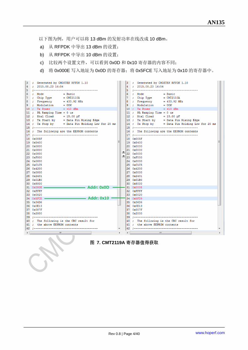
以下图为例,用户可以将 13 dBm 的发射功率在线改成 10 dBm。
a) 从 RFPDK 中导出 13 dBm 的设置;
b) 从 RFPDK 中导出 10 dBm 的设置;
c) 比较两个设置文件,可以看到 0x0D 和 0x10 寄存器的内容不同;
d) 将 0x000E 写入地址为 0x0D 的寄存器;将 0x5FCE 写入地址为 0x10 的寄存器中。
图 7. CMT2119A 寄存器值得获取
AN135
Rev 0.8 | Page 5/40
www.hoperf.com
3.3 CMT2119A 示例程序
本节将给出一些控制 CMT2119A 的示例程序,例如如何改变频率,改变发射功率等。更多示例
程序见相关附件。
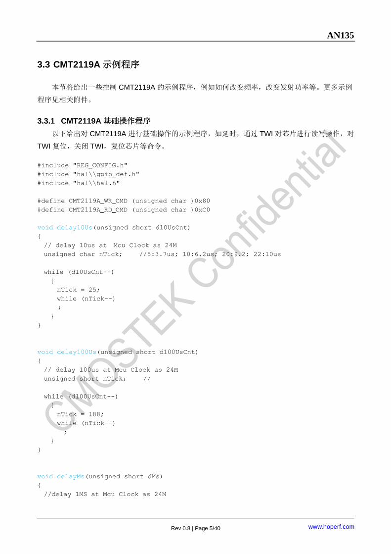
3.3.1 CMT2119A 基础操作程序
以下给出对 CMT2119A 进行基础操作的示例程序,如延时,通过 TWI 对芯片进行读写操作,对
TWI 复位,关闭 TWI,复位芯片等命令。
#include "REG_CONFIG.h"
#include "hal\\gpio_def.h"
#include "hal\\hal.h"
#define CMT2119A_WR_CMD (unsigned char )0x80
#define CMT2119A_RD_CMD (unsigned char )0xC0
void delay10Us(unsigned short d10UsCnt)
{
// delay 10us at Mcu Clock as 24M
unsigned char nTick; //5:3.7us; 10:6.2us; 20:9.2; 22:10us
while (d10UsCnt--)
{
nTick = 25;
while (nTick--)
;
}
}
void delay100Us(unsigned short d100UsCnt)
{
// delay 100us at Mcu Clock as 24M
unsigned short nTick; //
while (d100UsCnt--)
{
nTick = 188;
while (nTick--)
;
}
}
void delayMs(unsigned short dMs)
{
//delay 1MS at Mcu Clock as 24M
AN135
Rev 0.8 | Page 6/40
www.hoperf.com
unsigned short nTick;
while (dMs--)
{
nTick = 1895;
while (nTick--)
;
}
}
void TWI_WrByte(unsigned char SendByte)
{
unsigned char i = 0;
for (i = 0; i < 8; i++)
{
TWI_SCK_H();
if (SendByte & 0x80) //MSB
{
TWI_SDA_H();
}
else
{
TWI_SDA_L();
}
SendByte <<= 1;
delay10Us(1);
TWI_SCK_L();
delay10Us(1);
}
}
unsigned char TWI_RdByte(void)
{
unsigned char i;
unsigned char ReceiveByte = 0xff;
for (i = 0; i < 8; i++)
{
TWI_SCK_H();
ReceiveByte <<= 1;
delay10Us(1); //I2C_delay();
TWI_SCK_L();
if (TWI_SDA_read())
{
ReceiveByte |= 0x01;
}
else
{
ReceiveByte &= 0xFE;
AN135
Rev 0.8 | Page 7/40
www.hoperf.com
}
delay10Us(1); //I2C_delay();
}
return ReceiveByte;
}
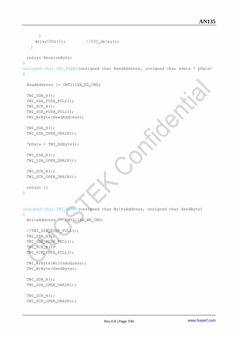
unsigned char TWI_RDREG(unsigned char ReadAddress, unsigned char xdata * pData)
{
ReadAddress |= CMT211XA_RD_CMD;
TWI_SDA_H();
TWI_SDA_PUSH_PULL();
TWI_SCK_H();
TWI_SCK_PUSH_PULL();
TWI_WrByte(ReadAddress);
TWI_SDA_H();
TWI_SDA_OPEN_DRAIN();
*pData = TWI_RdByte();
TWI_SDA_H();
TWI_SDA_OPEN_DRAIN();
TWI_SCK_H();
TWI_SCK_OPEN_DRAIN();
return 1;
}
unsigned char TWI_WRREG(unsigned char WriteAddress, unsigned char SendByte)
{
WriteAddress |= CMT211XA_WR_CMD;
//TWI_SDA_PUSH_PULL();
TWI_SDA_H();
TWI_SDA_PUSH_PULL();
TWI_SCK_H();
TWI_SCK_PUSH_PULL();
TWI_WrByte(WriteAddress);
TWI_WrByte(SendByte);
TWI_SDA_H();
TWI_SDA_OPEN_DRAIN();
TWI_SCK_H();
TWI_SCK_OPEN_DRAIN();
AN135
Rev 0.8 | Page 8/40
www.hoperf.com
return 1;
}
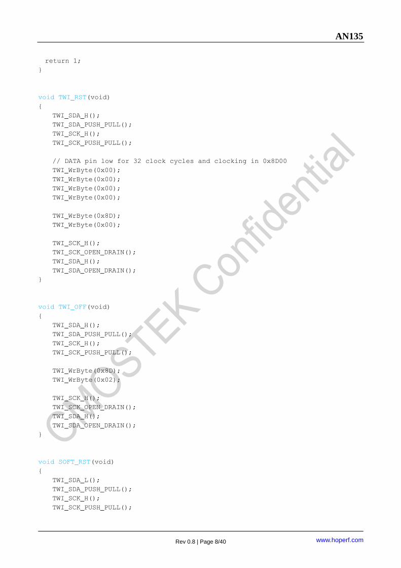
void TWI_RST(void)
{
TWI_SDA_H();
TWI_SDA_PUSH_PULL();
TWI_SCK_H();
TWI_SCK_PUSH_PULL();
// DATA pin low for 32 clock cycles and clocking in 0x8D00
TWI_WrByte(0x00);
TWI_WrByte(0x00);
TWI_WrByte(0x00);
TWI_WrByte(0x00);
TWI_WrByte(0x8D);
TWI_WrByte(0x00);
TWI_SCK_H();
TWI_SCK_OPEN_DRAIN();
TWI_SDA_H();
TWI_SDA_OPEN_DRAIN();
}
void TWI_OFF(void)
{
TWI_SDA_H();
TWI_SDA_PUSH_PULL();
TWI_SCK_H();
TWI_SCK_PUSH_PULL();
TWI_WrByte(0x8D);
TWI_WrByte(0x02);
TWI_SCK_H();
TWI_SCK_OPEN_DRAIN();
TWI_SDA_H();
TWI_SDA_OPEN_DRAIN();
}
void SOFT_RST(void)
{
TWI_SDA_L();
TWI_SDA_PUSH_PULL();
TWI_SCK_H();
TWI_SCK_PUSH_PULL();
AN135
Rev 0.8 | Page 9/40
www.hoperf.com
TWI_WrByte(0xBD);
TWI_WrByte(0x01);
TWI_SCK_H();
TWI_SCK_OPEN_DRAIN();
TWI_SDA_H();
TWI_SDA_OPEN_DRAIN();
}
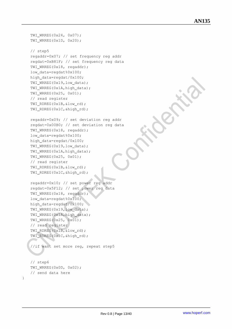
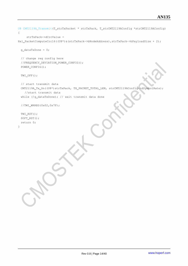
3.3.2 CMT2119A 修改频率,频偏,发射功率示例程序
以下给出对 CMT2119A 进行修改频率,修改发射功率及修改频偏等参数的操作的示例程序,也
给出对芯片进行配置后发射数据的示例程序。
void FREQUENCY_CONFIG(void)
{
unsigned char low_data,high_data;
unsigned char regaddr;
unsigned short regdat;
unsigned char low_rd,high_rd;
// step1
TWI_RST();
// step2
SOFT_RST();
delayMs(1);
// step3
TWI_WRREG(0x02, 0x78);
// step4
TWI_WRREG(0x2F, 0x80);
TWI_WRREG(0x35, 0xCA);
TWI_WRREG(0x36, 0xEB);
TWI_WRREG(0x37, 0x37);
TWI_WRREG(0x38, 0x82);
TWI_WRREG(0x12, 0x10);
TWI_WRREG(0x12, 0x00);
TWI_WRREG(0x24, 0x07);
TWI_WRREG(0x1D, 0x20);
// step5
regaddr=0x07; // set frequency reg addr
regdat=0xB81F; // set frequency reg data
TWI_WRREG(0x18, regaddr);
low_data=regdat%0x100;
high_data=regdat/0x100;
AN135
Rev 0.8 | Page 10/40
www.hoperf.com
TWI_WRREG(0x19,low_data);
TWI_WRREG(0x1A,high_data);
TWI_WRREG(0x25, 0x01);
// read register
TWI_RDREG(0x1B,&low_rd);
TWI_RDREG(0x1C,&high_rd);
//if want set more reg, repeat step5
// step6
TWI_WRREG(0x0D, 0x02);
// send data here
}
void DEVIATION_CONFIG(void)
{
unsigned char low_data,high_data;
unsigned char regaddr;
unsigned short regdat;
unsigned char low_rd,high_rd;
// step1
TWI_RST();
// step2
SOFT_RST();
delayMs(1);
// step3
TWI_WRREG(0x02, 0x78);
// step4
TWI_WRREG(0x2F, 0x80);
TWI_WRREG(0x35, 0xCA);
TWI_WRREG(0x36, 0xEB);
TWI_WRREG(0x37, 0x37);
TWI_WRREG(0x38, 0x82);
TWI_WRREG(0x12, 0x10);
TWI_WRREG(0x12, 0x00);
TWI_WRREG(0x24, 0x07);
TWI_WRREG(0x1D, 0x20);
// step5
regaddr=0x09; // set deviation reg addr
regdat=0x00B0; // set deviation reg data
AN135
Rev 0.8 | Page 11/40
www.hoperf.com
TWI_WRREG(0x18, regaddr);
low_data=regdat%0x100;
high_data=regdat/0x100;
TWI_WRREG(0x19,low_data);
TWI_WRREG(0x1A,high_data);
TWI_WRREG(0x25, 0x01);
// read register
TWI_RDREG(0x1B,&low_rd);
TWI_RDREG(0x1C,&high_rd);
//if want set more reg, repeat step5
// step6
TWI_WRREG(0x0D, 0x02);
// send data here
}
void POWER_CONFIG(void)
{
unsigned char low_data,high_data;
unsigned char regaddr;
unsigned short regdat;
unsigned char low_rd,high_rd;
// step1
TWI_RST();
// step2
SOFT_RST();
delayMs(1);
// step3
TWI_WRREG(0x02, 0x78);
// step4
TWI_WRREG(0x2F, 0x80);
TWI_WRREG(0x35, 0xCA);
TWI_WRREG(0x36, 0xEB);
TWI_WRREG(0x37, 0x37);
TWI_WRREG(0x38, 0x82);
TWI_WRREG(0x12, 0x10);
TWI_WRREG(0x12, 0x00);
TWI_WRREG(0x24, 0x07);
TWI_WRREG(0x1D, 0x20);
AN135
Rev 0.8 | Page 12/40
www.hoperf.com
// step5
regaddr=0x10; // set power reg addr
regdat=0x5F12; // set power reg data
TWI_WRREG(0x18, regaddr);
low_data=regdat%0x100;
high_data=regdat/0x100;
TWI_WRREG(0x19,low_data);
TWI_WRREG(0x1A,high_data);
TWI_WRREG(0x25, 0x01);
// read register
TWI_RDREG(0x1B,&low_rd);
TWI_RDREG(0x1C,&high_rd);
//if want set more reg, repeat step5
// step6
TWI_WRREG(0x0D, 0x02);
// send data here
}
void FREQUENCY_DEVIATION_POWER_CONFIG(void)
{
unsigned char low_data,high_data;
unsigned char regaddr;
unsigned short regdat;
unsigned char low_rd,high_rd;
// step1
TWI_RST();
// step2
SOFT_RST();
delayMs(1);
// step3
TWI_WRREG(0x02, 0x78);
// step4
TWI_WRREG(0x2F, 0x80);
TWI_WRREG(0x35, 0xCA);
TWI_WRREG(0x36, 0xEB);
TWI_WRREG(0x37, 0x37);
TWI_WRREG(0x38, 0x82);
TWI_WRREG(0x12, 0x10);
TWI_WRREG(0x12, 0x00);
AN135
Rev 0.8 | Page 13/40
www.hoperf.com
TWI_WRREG(0x24, 0x07);
TWI_WRREG(0x1D, 0x20);
// step5
regaddr=0x07; // set frequency reg addr
regdat=0xB81F; // set frequency reg data
TWI_WRREG(0x18, regaddr);
low_data=regdat%0x100;
high_data=regdat/0x100;
TWI_WRREG(0x19,low_data);
TWI_WRREG(0x1A,high_data);
TWI_WRREG(0x25, 0x01);
// read register
TWI_RDREG(0x1B,&low_rd);
TWI_RDREG(0x1C,&high_rd);
regaddr=0x09; // set deviation reg addr
regdat=0x00B0; // set deviation reg data
TWI_WRREG(0x18, regaddr);
low_data=regdat%0x100;
high_data=regdat/0x100;
TWI_WRREG(0x19,low_data);
TWI_WRREG(0x1A,high_data);
TWI_WRREG(0x25, 0x01);
// read register
TWI_RDREG(0x1B,&low_rd);
TWI_RDREG(0x1C,&high_rd);
regaddr=0x10; // set power reg addr
regdat=0x5F12; // set power reg data
TWI_WRREG(0x18, regaddr);
low_data=regdat%0x100;
high_data=regdat/0x100;
TWI_WRREG(0x19,low_data);
TWI_WRREG(0x1A,high_data);
TWI_WRREG(0x25, 0x01);
// read register
TWI_RDREG(0x1B,&low_rd);
TWI_RDREG(0x1C,&high_rd);
//if want set more reg, repeat step5
// step6
TWI_WRREG(0x0D, 0x02);
// send data here
}
AN135
Rev 0.8 | Page 14/40
www.hoperf.com
U8 CMT2119A_Transmit(T_strTxPacket * strTxPack, T_strCMT2119AConfig *strCMT2119AConfig)
{
strTxPack->dCrcValue =
Hal_PacketComputeCrc16((U8*)&(strTxPack->bNodeAddress),strTxPack->bPayloadSize + 2);
g_dataTxDone = 0;
// change reg config here
//FREQUENCY_DEVIATION_POWER_CONFIG();
POWER_CONFIG();
TWI_OFF();
// start transmit data
CMT2119A_Tx_On((U8*)strTxPack, TX_PACKET_TOTAL_LEN, strCMT2119AConfig->dSymbolRate);
//start transmit data
while (!g_dataTxDone); // wait transmit data done
//TWI_WRREG(0x02,0x7F);
TWI_RST();
SOFT_RST();
return 0;
}
AN135
Rev 0.8 | Page 15/40
www.hoperf.com
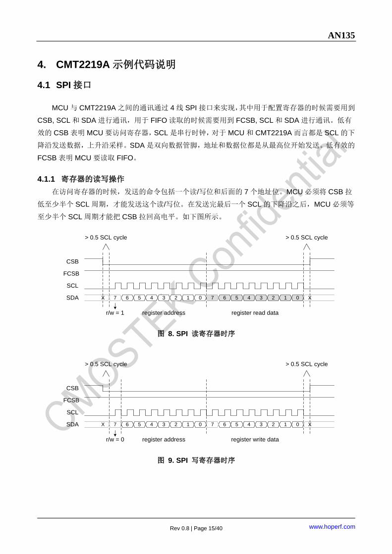
4. CMT2219A 示例代码说明
4.1 SPI 接口
MCU 与 CMT2219A 之间的通讯通过 4 线 SPI 接口来实现,其中用于配置寄存器的时候需要用到
CSB, SCL 和 SDA 进行通讯,用于 FIFO 读取的时候需要用到 FCSB, SCL 和 SDA 进行通讯。低有
效的 CSB 表明 MCU 要访问寄存器,SCL 是串行时钟,对于 MCU 和 CMT2219A 而言都是 SCL 的下
降沿发送数据,上升沿采样。SDA 是双向数据管脚,地址和数据位都是从最高位开始发送。低有效的
FCSB 表明 MCU 要读取 FIFO。
4.1.1 寄存器的读写操作
在访问寄存器的时候,发送的命令包括一个读/写位和后面的 7 个地址位。MCU 必须将 CSB 拉
低至少半个 SCL 周期,才能发送这个读/写位。在发送完最后一个 SCL 的下降沿之后,MCU 必须等
至少半个 SCL 周期才能把 CSB 拉回高电平。如下图所示。
SCL
CSB
SDA X 01234567 X
register address register read data
01234567
r/w = 1
FCSB
> 0.5 SCL cycle > 0.5 SCL cycle
图 8. SPI 读寄存器时序
SCL
CSB
SDA X X 01234567 01234567
register address register write data
FCSB
r/w = 0
> 0.5 SCL cycle > 0.5 SCL cycle
图 9. SPI 写寄存器时序
AN135
Rev 0.8 | Page 16/40
www.hoperf.com
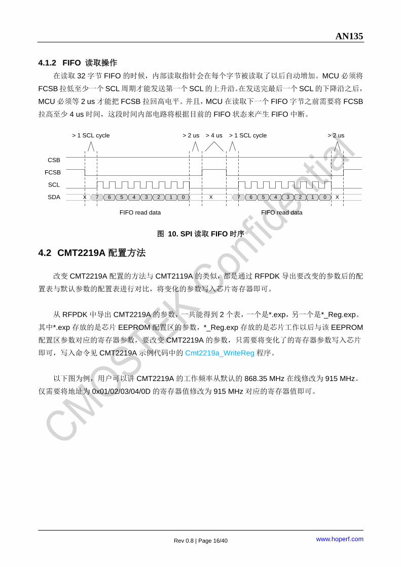
4.1.2 FIFO 读取操作
在读取 32 字节 FIFO 的时候,内部读取指针会在每个字节被读取了以后自动增加。MCU 必须将
FCSB拉低至少一个SCL周期才能发送第一个 SCL的上升沿。在发送完最后一个 SCL的下降沿之后,
MCU 必须等 2 us 才能把 FCSB 拉回高电平。并且,MCU 在读取下一个 FIFO 字节之前需要将 FCSB
拉高至少 4 us 时间,这段时间内部电路将根据目前的 FIFO 状态来产生 FIFO 中断。
SCL
FCSB
SDA X X
FIFO read data
01234567 01234567X
FIFO read data
CSB
> 1 SCL cycle > 4 us> 2 us > 2 us> 1 SCL cycle
图 10. SPI 读取 FIFO 时序
4.2 CMT2219A 配置方法
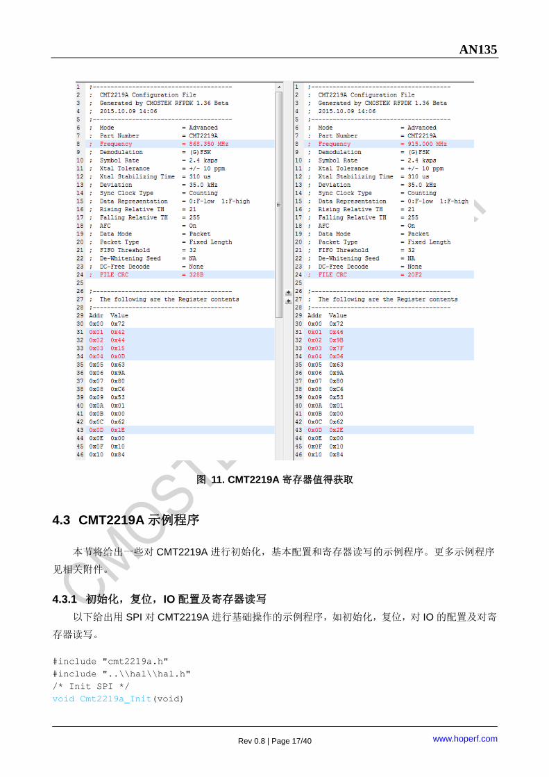
改变 CMT2219A 配置的方法与 CMT2119A 的类似,都是通过 RFPDK 导出要改变的参数后的配
置表与默认参数的配置表进行对比,将变化的参数写入芯片寄存器即可。
从 RFPDK 中导出 CMT2219A 的参数,一共能得到 2 个表,一个是*.exp,另一个是*_Reg.exp。
其中*.exp 存放的是芯片 EEPROM 配置区的参数,*_Reg.exp 存放的是芯片工作以后与该 EEPROM
配置区参数对应的寄存器参数,要改变 CMT2219A 的参数,只需要将变化了的寄存器参数写入芯片
即可,写入命令见 CMT2219A 示例代码中的 Cmt2219a_WriteReg 程序。
以下图为例,用户可以讲 CMT2219A 的工作频率从默认的 868.35 MHz 在线修改为 915 MHz。
仅需要将地址为 0x01/02/03/04/0D 的寄存器值修改为 915 MHz 对应的寄存器值即可。
AN135
Rev 0.8 | Page 17/40
www.hoperf.com
图 11. CMT2219A 寄存器值得获取
4.3 CMT2219A 示例程序
本节将给出一些对 CMT2219A 进行初始化,基本配置和寄存器读写的示例程序。更多示例程序
见相关附件。
4.3.1 初始化,复位,IO 配置及寄存器读写
以下给出用 SPI 对 CMT2219A 进行基础操作的示例程序,如初始化,复位,对 IO 的配置及对寄
存器读写。
#include "cmt2219a.h"
#include "..\\hal\\hal.h"
/* Init SPI */
void Cmt2219a_Init(void)
AN135
Rev 0.8 | Page 18/40
www.hoperf.com
{
SPI3_Init();
}
U8 Cmt2219a_ReadReg(U8 addr)
{
U8 value;
SPI3_ReadByte(addr, &value, 1);
return value;
}
U8 Cmt2219a_WriteReg(U8 addr, U8 value)
{
SPI3_WriteByte(addr, value);
return 0;
}
U8 Cmt2219a_WriteNReg(U8 addr, U8 xdata *dat, U8 len)
{
U8 i, tempdat;
for (i = 0; i < len; i++)
{
SPI3_WriteByte(addr, dat[i]);
SPI3_ReadByte(addr, &tempdat, 1);
if (dat[i] != tempdat)
return 1;
addr++;
}
return 0;
}
U8 Cmt2219a_ReadNReg(U8 addr, U8 xdata *dat, U8 len)
{
U8 tempdat, i;
for (i = 0; i < len; i++)
{
SPI3_ReadByte(addr, &tempdat, 1);
dat[i] = tempdat;
addr++;
}
return 0;
}
AN135
Rev 0.8 | Page 19/40
www.hoperf.com
/*! ********************************************************
* @desc:
* Writing 0xFF into this register will generate a soft_reset command to the device.
* Setting this register to any values other than 0xFF will not take any effect.
* The soft reset has the same effect of POR.
* After the soft reset, the chip will go through the power-up sequence and then
enter the SLEEP Mode.
* After soft resetting the chip, the MCU shall wait 10 ms before performing any
other controls to the chip.
* *********************************************************/
void Cmt2219a_SoftReset(void)
{
SPI3_WriteByte(REG_SOFTRST, 0xFF);
}
/*! ********************************************************
* @desc:
* Select which signal is assigned to GPO1.
* @param:
* GPO1_SEL_NRSTO(0): nRSTO is output via GPO1 (default).
* GPO1_SEL_INT1(1): INT1 is output via GPO1.
* GPO1_SEL_INT2(2): INT2 is output via GPO1.
* GPO1_SEL_DOUT(3): DOUT is output via GPO1.
* *********************************************************/
U8 Cmt2219a_SetGpo1Sel(U8 dat)
{
// GPO1_SEL: IO_SEL<1:0>
U8 tempdat;
SPI3_ReadByte(REG_IO_SEL, &tempdat, 1);
tempdat &= ~0x03;
tempdat |= dat;
SPI3_WriteByte(REG_IO_SEL, tempdat);
return 0;
}
/*! ********************************************************
* @desc:
* Select which signal is assigned to GPO2.
* @param:
* GPO2_SEL_INT1(0): INT1 is output via GPO2 (default).
* GPO2_SEL_INT2(1): INT2 is output via GPO2.
* GPO2_SEL_DCLK(2): DCLK is output via GPO2.
* GPO2_SEL_LOGIC_ZERO(3): logic „0‟ is output via GPO2.
* *********************************************************/
U8 Cmt2219a_SetGpo2Sel(U8 dat)
AN135
Rev 0.8 | Page 20/40
www.hoperf.com
{
// GPO2_SEL: IO_SEL<3:2>
U8 tempdat;
SPI3_ReadByte(REG_IO_SEL, &tempdat, 1);
tempdat &= ~(0x03 << 2);
tempdat |= (dat << 2);
SPI3_WriteByte(REG_IO_SEL, tempdat);
return 0;
}
/*! ********************************************************
* @desc:
* Select which signal is assigned to GPO3.
* @param:
* GPO3_SEL_CLKO(0): CLKO is output via GPO3 (default).
* GPO3_SEL_INT1(1): INT1 is output via GPO3.
* GPO3_SEL_INT2(2): INT2 is output via GPO3.
* GPO3_SEL_DOUT(3): DOUT is output via GPO3.
* *********************************************************/
U8 Cmt2219a_SetGpo3Sel(U8 dat)
{
// GPO3_SEL: IO_SEL<5:4>
U8 tempdat;
SPI3_ReadByte(REG_IO_SEL, &tempdat, 1);
tempdat &= ~(0x03 << 4);
tempdat |= (dat << 4);
SPI3_WriteByte(REG_IO_SEL, tempdat);
return 0;
}
/*! ********************************************************
* @desc:
* Select which signal is assigned to GPO4.
* @param:
* GPO4_SEL_DOUT(0): DOUT is output via GPO4 (default).
* GPO4_SEL_INT1(1): INT1 is output via GPO4.
* GPO4_SEL_INT2(2): INT2 is output via GPO4.
* GPO4_SEL_DCLK(3): DCLK is output via GPO4.
* *********************************************************/
U8 Cmt2219a_SetGpo4Sel(U8 dat)
{
// GPO4_SEL: IO_SEL<7:6>
U8 tempdat;
SPI3_ReadByte(REG_IO_SEL, &tempdat, 1);
AN135
Rev 0.8 | Page 21/40
www.hoperf.com
tempdat &= ~(0x03 << 6);
tempdat |= (dat << 6);
SPI3_WriteByte(REG_IO_SEL, tempdat);
return 0;
}
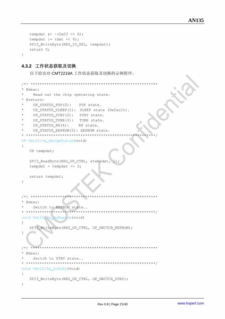
4.3.2 工作状态获取及切换
以下给出对 CMT2219A 工作状态获取及切换的示例程序。
/*! ********************************************************
* @desc:
* Read out the chip operating state.
* @return:
* OP_STATUS_PUP(0): PUP state.
* OP_STATUS_SLEEP(1): SLEEP state (Default).
* OP_STATUS_STBY(2): STBY state.
* OP_STATUS_TUNE(3): TUNE state.
* OP_STATUS_RX(4): RX state.
* OP_STATUS_EEPROM(5): EEPROM state.
* *********************************************************/
U8 Cmt2219a_GetOpStatus(void)
{
U8 tempdat;
SPI3_ReadByte(REG_OP_CTRL, &tempdat, 1);
tempdat = tempdat >> 5;
return tempdat;
}
/*! ********************************************************
* @desc:
* Switch to EEPROM state..
* *********************************************************/
void Cmt2219a_GoEeprom(void)
{
SPI3_WriteByte(REG_OP_CTRL, OP_SWITCH_EEPROM);
}
/*! ********************************************************
* @desc:
* Switch to STBY state..
* *********************************************************/
void Cmt2219a_GoStby(void)
{
SPI3_WriteByte(REG_OP_CTRL, OP_SWITCH_STBY);
}
AN135
Rev 0.8 | Page 22/40
www.hoperf.com
/*! ********************************************************
* @desc:
* Switch to TUNE state..
* *********************************************************/
void Cmt2219a_GoTune(void)
{
SPI3_WriteByte(REG_OP_CTRL, OP_SWITCH_TUNE);
}
/*! ********************************************************
* @desc:
* Switch to RX state..
* *********************************************************/
void Cmt2219a_GoRx(void)
{
SPI3_WriteByte(REG_OP_CTRL, OP_SWITCH_RX);
}
/*! ********************************************************
* @desc:
* Switch to SLEEP state.
* *********************************************************/
void Cmt2219a_GoSleep(void)
{
SPI3_WriteByte(REG_OP_CTRL, OP_SWITCH_SLEEP);
}
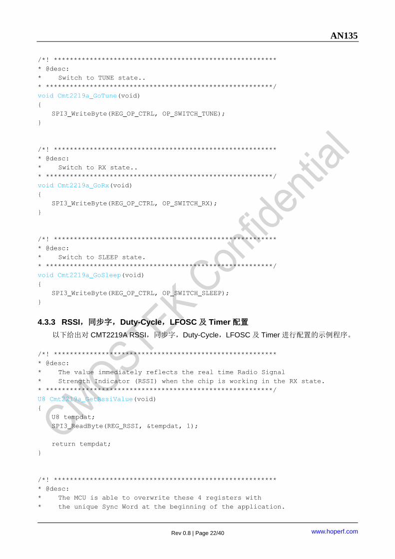
4.3.3 RSSI,同步字,Duty-Cycle,LFOSC 及 Timer 配置
以下给出对 CMT2219A RSSI,同步字,Duty-Cycle,LFOSC 及 Timer 进行配置的示例程序。
/*! ********************************************************
* @desc:
* The value immediately reflects the real time Radio Signal
* Strength Indicator (RSSI) when the chip is working in the RX state.
* *********************************************************/
U8 Cmt2219a_GetRssiValue(void)
{
U8 tempdat;
SPI3_ReadByte(REG_RSSI, &tempdat, 1);
return tempdat;
}
/*! ********************************************************
* @desc:
* The MCU is able to overwrite these 4 registers with
* the unique Sync Word at the beginning of the application.
AN135
Rev 0.8 | Page 23/40
www.hoperf.com
* *********************************************************/
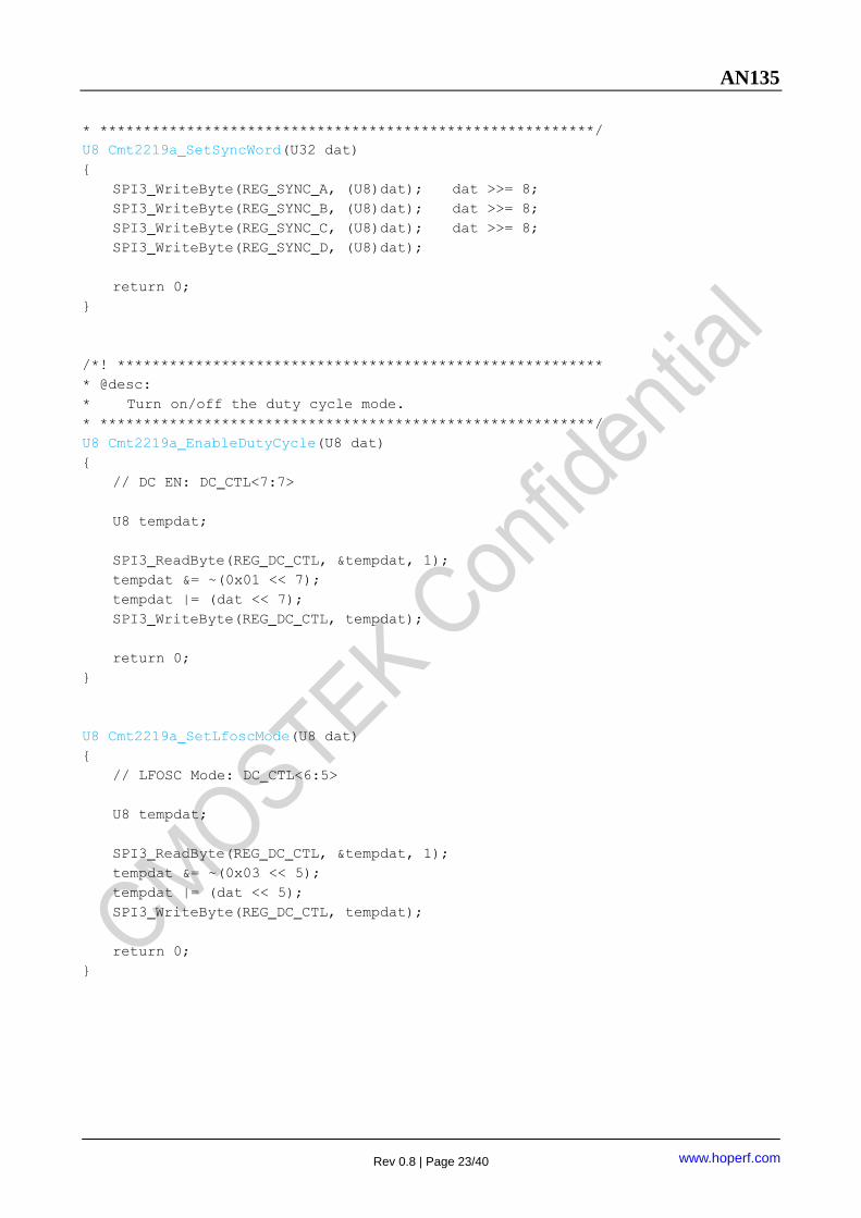
U8 Cmt2219a_SetSyncWord(U32 dat)
{
SPI3_WriteByte(REG_SYNC_A, (U8)dat); dat >>= 8;
SPI3_WriteByte(REG_SYNC_B, (U8)dat); dat >>= 8;
SPI3_WriteByte(REG_SYNC_C, (U8)dat); dat >>= 8;
SPI3_WriteByte(REG_SYNC_D, (U8)dat);
return 0;
}
/*! ********************************************************
* @desc:
* Turn on/off the duty cycle mode.
* *********************************************************/
U8 Cmt2219a_EnableDutyCycle(U8 dat)
{
// DC EN: DC_CTL<7:7>
U8 tempdat;
SPI3_ReadByte(REG_DC_CTL, &tempdat, 1);
tempdat &= ~(0x01 << 7);
tempdat |= (dat << 7);
SPI3_WriteByte(REG_DC_CTL, tempdat);
return 0;
}
U8 Cmt2219a_SetLfoscMode(U8 dat)
{
// LFOSC Mode: DC_CTL<6:5>
U8 tempdat;
SPI3_ReadByte(REG_DC_CTL, &tempdat, 1);
tempdat &= ~(0x03 << 5);
tempdat |= (dat << 5);
SPI3_WriteByte(REG_DC_CTL, tempdat);
return 0;
}
AN135
Rev 0.8 | Page 24/40
www.hoperf.com
/*! ********************************************************
* @desc:
* Turn on/off the sleep timer.
* *********************************************************/
U8 Cmt2219a_EnableSleepTimer(U8 dat)
{
// SL_CTL: SLP EN<7:7>
U8 tempdat;
SPI3_ReadByte(REG_SL_CTL, &tempdat, 1);
tempdat &= ~(0x01 << 7);
tempdat |= (dat << 7);
SPI3_WriteByte(REG_SL_CTL, tempdat);
return 0;
}
/*! ********************************************************
* @desc:
* Turn on/off the receive timer.
* *********************************************************/
U8 Cmt2219a_EnableRecvTimer(U8 dat)
{
// RX_CTL: RX EN<7:7>
U8 tempdat;
SPI3_ReadByte(REG_RX_CTL, &tempdat, 1);
tempdat &= ~(0x01 << 7);
tempdat |= (dat << 7);
SPI3_WriteByte(REG_RX_CTL, tempdat);
return 0;
}
4.3.4 中断相关配置
以下给出对 CMT2219A 中断进行相关配置的示例程序。
/*! ********************************************************
* @param:
* 0: Disable the sleep timer timeout interrupt (default).
* 1: Enable the sleep timer timeout interrupt.
* *********************************************************/
U8 Cmt2219a_EnableSleepTimeoutInt(U8 dat)
{
// SL_TMO_EN: INT_EN<7:7>
U8 tempdat;
AN135
Rev 0.8 | Page 25/40
www.hoperf.com
SPI3_ReadByte(REG_INT_EN, &tempdat, 1);
tempdat &= ~(0x01 << 7);
tempdat |= (dat << 7);
SPI3_WriteByte(REG_INT_EN, tempdat);
return 0;
}
/*! ********************************************************
* @param:
* 0: Disable the receive timer timeout interrupt (default).
* 1: Enable the receive timer timeout interrupt.
* *********************************************************/
U8 Cmt2219a_EnableRecvTimeoutInt(U8 dat)
{
// RX_TMO_EN: INT_EN<6:6>
U8 tempdat;
SPI3_ReadByte(REG_INT_EN, &tempdat, 1);
tempdat &= ~(0x01 << 6);
tempdat |= (dat << 6);
SPI3_WriteByte(REG_INT_EN, tempdat);
return 0;
}
/*! ********************************************************
* @param:
* 0: Disable the RSSI valid interrupt (default).
* 1: Enable the RSSI valid interrupt.
* *********************************************************/
U8 Cmt2219a_EnableRssiValidInt(U8 dat)
{
// RSSI_VLD_EN: INT_EN<5:5>
U8 tempdat;
SPI3_ReadByte(REG_INT_EN, &tempdat, 1);
tempdat &= ~(0x01 << 5);
tempdat |= (dat << 5);
SPI3_WriteByte(REG_INT_EN, tempdat);
return 0;
}
AN135
Rev 0.8 | Page 26/40
www.hoperf.com
/*! ********************************************************
* @param:
* 0: Disable the preamble detection pass interrupt (default).
* 1: Enable the preamble detection pass interrupt.
* *********************************************************/
U8 Cmt2219a_EnablePreamblePassInt(U8 dat)
{
// PREAM_PS_EN: INT_EN<4:4>
U8 tempdat;
SPI3_ReadByte(REG_INT_EN, &tempdat, 1);
tempdat &= ~(0x01 << 4);
tempdat |= (dat << 4);
SPI3_WriteByte(REG_INT_EN, tempdat);
return 0;
}
/*! ********************************************************
* @param:
* 0: Disable the sync word detection pass interrupt (default).
* 1: Enable the sync word detection pass interrupt.
* *********************************************************/
U8 Cmt2219a_EnableSyncWordPassInt(U8 dat)
{
// SYNC_PS_EN: INT_EN<3:3>
U8 tempdat;
SPI3_ReadByte(REG_INT_EN, &tempdat, 1);
tempdat &= ~(0x01 << 3);
tempdat |= (dat << 3);
SPI3_WriteByte(REG_INT_EN, tempdat);
return 0;
}
/*! ********************************************************
* @param:
* 0: Disable the node ID detection pass interrupt (default).
* 1: Enable the node ID detection pass interrupt.
* *********************************************************/
U8 Cmt2219a_EnableNodeIdPassInt(U8 dat)
{
// NODE_PS_EN: INT_EN<2:2>
U8 tempdat;
AN135
Rev 0.8 | Page 27/40
www.hoperf.com
SPI3_ReadByte(REG_INT_EN, &tempdat, 1);
tempdat &= ~(0x01 << 2);
tempdat |= (dat << 2);
SPI3_WriteByte(REG_INT_EN, tempdat);
return 0;
}
/*! ********************************************************
* @param:
* 0: Disable the CRC validation pass interrupt (default).
* 1: Enable the CRC validation pass interrupt.
* *********************************************************/
U8 Cmt2219a_EnableCrcPassInt(U8 dat)
{
// CRC_PS_EN: INT_EN<1:1>
U8 tempdat;
SPI3_ReadByte(REG_INT_EN, &tempdat, 1);
tempdat &= ~(0x01 << 1);
tempdat |= (dat << 1);
SPI3_WriteByte(REG_INT_EN, tempdat);
return 0;
}
/*! ********************************************************
* @param:
* 0: Disable the packet receive finish interrupt (default).
* 1: Enable the packet receive finish interrupt.
* *********************************************************/
U8 Cmt2219a_EnablePacketDoneInt(U8 dat)
{
// PKT_DONE_EN: INT_EN<0:0>
U8 tempdat;
SPI3_ReadByte(REG_INT_EN, &tempdat, 1);
tempdat &= ~0x01;
tempdat |= dat;
SPI3_WriteByte(REG_INT_EN, tempdat);
return 0;
}
AN135
Rev 0.8 | Page 28/40
www.hoperf.com
/*! ********************************************************
* @desc:
* Select which interrupt is observable on the INT2.
* *********************************************************/
U8 Cmt2219a_SetInt1(U8 dat)
{
// INT1_CTL: INTCTL_A<3:0>
U8 tempdat;
SPI3_ReadByte(REG_INTCTL_A, &tempdat, 1);
tempdat &= ~0x0F;
tempdat |= dat;
SPI3_WriteByte(REG_INTCTL_A, tempdat);
return 0;
}
/*! ********************************************************
* @desc:
* Select which interrupt is observable on the INT1.
* *********************************************************/
U8 Cmt2219a_SetInt2(U8 dat)
{
// INT2_CTL: INTCTL_A<7:4>
U8 tempdat;
SPI3_ReadByte(REG_INTCTL_A, &tempdat, 1);
tempdat &= ~(0x0F << 4);
tempdat |= (dat << 4);
SPI3_WriteByte(REG_INTCTL_A, tempdat);
return 0;
}
/*! ********************************************************
* @param:
* 0: Keep the sleep timer timeout interrupt (default).
* 1: Clear the sleep timer timeout interrupt.
* *********************************************************/
U8 Cmt2219a_ClearSleepTimeoutInt(U8 dat)
{
// SL_TMO_CLR: INTCTL_B<7:7>
U8 tempdat;
SPI3_ReadByte(REG_INTCTL_B, &tempdat, 1);
AN135
Rev 0.8 | Page 29/40
www.hoperf.com
tempdat &= ~(0x01 << 7);
tempdat |= (dat << 7);
SPI3_WriteByte(REG_INTCTL_B, tempdat);
return 0;
}
/*! ********************************************************
* @param:
* 0: Keep the receive timer timeout interrupt (default).
* 1: Clear the receive timer timeout interrupt.
* *********************************************************/
U8 Cmt2219a_ClearRecvTimeoutInt(U8 dat)
{
// RX_TMO_CLR: INTCTL_B<6:6>
U8 tempdat;
SPI3_ReadByte(REG_INTCTL_B, &tempdat, 1);
tempdat &= ~(0x01 << 6);
tempdat |= (dat << 6);
SPI3_WriteByte(REG_INTCTL_B, tempdat);
return 0;
}
/*! ********************************************************
* @param:
* 0: Keep the RSSI valid interrupt (default).
* 1: Clear the RSSI valid interrupt.
* *********************************************************/
U8 Cmt2219a_ClearRssiValidInt(U8 dat)
{
// RSSI_VLD_CLR: INTCTL_B<5:5>
U8 tempdat;
SPI3_ReadByte(REG_INTCTL_B, &tempdat, 1);
tempdat &= ~(0x01 << 5);
tempdat |= (dat << 5);
SPI3_WriteByte(REG_INTCTL_B, tempdat);
return 0;
}
AN135
Rev 0.8 | Page 30/40
www.hoperf.com
/*! ********************************************************
* @param:
* 0: Keep the preamble detection pass interrupt (default).
* 1: Clear the preamble detection pass interrupt.
* *********************************************************/
U8 Cmt2219a_ClearPreamblePassInt(U8 dat)
{
// PREAM_PS_CLR: INTCTL_B<4:4>
U8 tempdat;
SPI3_ReadByte(REG_INTCTL_B, &tempdat, 1);
tempdat &= ~(0x01 << 4);
tempdat |= (dat << 4);
SPI3_WriteByte(REG_INTCTL_B, tempdat);
return 0;
}
/*! ********************************************************
* @param:
* 0: Keep the sync word detection pass interrupt (default).
* 1: Clear the sync word detection pass interrupt.
* *********************************************************/
U8 Cmt2219a_ClearSyncWordPassInt(U8 dat)
{
// SYNC_PS_CLR: INTCTL_B<3:3>
U8 tempdat;
SPI3_ReadByte(REG_INTCTL_B, &tempdat, 1);
tempdat &= ~(0x01 << 3);
tempdat |= (dat << 3);
SPI3_WriteByte(REG_INTCTL_B, tempdat);
return 0;
}
/*! ********************************************************
* @param:
* 0: Keep the node ID detection pass interrupt (default).
* 1: Clear the node ID detection pass interrupt.
* *********************************************************/
U8 Cmt2219a_ClearNodeIdPassInt(U8 dat)
{
// NODE_PS_CLR: INTCTL_B<2:2>
U8 tempdat;
AN135
Rev 0.8 | Page 31/40
www.hoperf.com
SPI3_ReadByte(REG_INTCTL_B, &tempdat, 1);
tempdat &= ~(0x01 << 2);
tempdat |= (dat << 2);
SPI3_WriteByte(REG_INTCTL_B, tempdat);
return 0;
}
/*! ********************************************************
* @param:
* 0: Keep the CRC validation pass interrupt (default).
* 1: Clear the CRC validation pass interrupt.
* *********************************************************/
U8 Cmt2219a_ClearCrcPassInt(U8 dat)
{
// CRC_PS_CLR: INTCTL_B<1:1>
U8 tempdat;
SPI3_ReadByte(REG_INTCTL_B, &tempdat, 1);
tempdat &= ~(0x01 << 1);
tempdat |= (dat << 1);
SPI3_WriteByte(REG_INTCTL_B, tempdat);
return 0;
}
/*! ********************************************************
* @param:
* 0: Keep the packet receive finish interrupt (default).
* 1: Clear the packet receive finish interrupt.
* *********************************************************/
U8 Cmt2219a_ClearPacketDoneInt(U8 dat)
{
// PKT_DONE_CLR: INTCTL_B<0:0>
U8 tempdat;
SPI3_ReadByte(REG_INTCTL_B, &tempdat, 1);
tempdat &= ~0x01;
tempdat |= dat;
SPI3_WriteByte(REG_INTCTL_B, tempdat);
return 0;
}
AN135
Rev 0.8 | Page 32/40
www.hoperf.com
4.3.5 标志位相关配置
以下给出对 CMT2219A 标志位(Flag)进行相关配置的示例程序。
/*! ********************************************************
* @desc:
* This interrupt is generated when the sleep timer
* is turned on and the SL_TMO_EN is set to 1.
* The flag goes high at the sleep timer timeout.
* It can be cleared by setting the SL_TMO_CLR to 1.
* *********************************************************/
U8 Cmt2219a_GetSleepTimeoutFlag()
{
// SL_TMO_FLG: INTCTL_C<7:7>
U8 tempdat;
SPI3_ReadByte(REG_INTCTL_C, &tempdat, 1);
return ( (tempdat >> 7) & 0x01 );
}
/*! ********************************************************
* @desc:
* This interrupt is generated when the receive timer
* is turned on and the RX_TMO_EN is set to 1.
* The flag goes high at the receive timer timeout.
* It can be cleared by setting the RX_TMO_CLR to 1.
* *********************************************************/
U8 Cmt2219a_GetRecvTimeoutFlag()
{
// RX_TMO_FLG: INTCTL_C<6:6>
U8 tempdat;
SPI3_ReadByte(REG_INTCTL_C, &tempdat, 1);
return ( (tempdat >> 6) & 0x01 );
}
/*! ********************************************************
* @desc:
* This interrupt is generated when (G)FSK demodulation
* is used and the RSSI_VLD_EN is set to 1.
* The flag goes high when the RSSI exceeds the FSK Trigger Threshold.
* It can be cleared by setting the RSSI_VLD_CLR to 1.
* *********************************************************/
U8 Cmt2219a_GetRssiValidFlag()
{
// RSSI_VLD_FLG: INTCTL_C<5:5>
AN135
Rev 0.8 | Page 33/40
www.hoperf.com
U8 tempdat;
SPI3_ReadByte(REG_INTCTL_C, &tempdat, 1);
return ( (tempdat >> 5) & 0x01 );
}
/*! ********************************************************
* @desc:
* This interrupt is generated when the preamble validation
* is passed and the PREAM_PS_EN is set to 1.
* It can be cleared by setting the PREAM_PS_CLR to 1.
* *********************************************************/
U8 Cmt2219a_GetPreamblePassFlag()
{
// PREAM_PS_FLG: INTCTL_C<4:4>
U8 tempdat;
SPI3_ReadByte(REG_INTCTL_C, &tempdat, 1);
return ( (tempdat >> 4) & 0x01 );
}
/*! ********************************************************
* @desc:
* This interrupt is generated when the sync word validation
* is passed and the SYNC_PS_EN is set to 1.
* It can be cleared by setting the SYNC_PS_CLR to 1.
* *********************************************************/
U8 Cmt2219a_GetSyncWordPassFlag()
{
// SYNC_PS_FLG: INTCTL_C<3:3>
U8 tempdat;
SPI3_ReadByte(REG_INTCTL_C, &tempdat, 1);
return ( (tempdat >> 3) & 0x01 );
}
/*! ********************************************************
* @desc:
* This interrupt is generated when the node ID validation
* is passed in the packet mode and the NODE_PS_EN is set to 1.
* It can be cleared by setting the NODE_PS_CLR to 1.
* *********************************************************/
U8 Cmt2219a_GetNodeIdPassFlag()
{
// NODE_PS_FLG: INTCTL_C<2:2>
U8 tempdat;
AN135
Rev 0.8 | Page 34/40
www.hoperf.com
SPI3_ReadByte(REG_INTCTL_C, &tempdat, 1);
return ( (tempdat >> 2) & 0x01 );
}
/*! ********************************************************
* @desc:
* This interrupt is generated when the CRC validation
* is passed in the packet mode and the CRC_PS_EN is set to 1.
* It can be cleared by setting the CRC_PS_CLR to 1.
* *********************************************************/
U8 Cmt2219a_GetCrcPassFlag()
{
// CRC_PS_FLG: INTCTL_C<1:1>
U8 tempdat;
SPI3_ReadByte(REG_INTCTL_C, &tempdat, 1);
return ( (tempdat >> 1) & 0x01 );
}
/*! ********************************************************
* @desc:
* This interrupt is generated when a packet is received (regardless of
* the CRC validation) in the packet mode and the PKT_DONE_EN is set to 1.
* It can be cleared by setting the PKT_DONE_CLR to 1.
* *********************************************************/
U8 Cmt2219a_GetPacketDoneFlag()
{
// PKT_DONE_FLG: INTCTL_C<0:0>
U8 tempdat;
SPI3_ReadByte(REG_INTCTL_C, &tempdat, 1);
return ( tempdat & 0x01 );
}
/*! ********************************************************
* @desc:
* This interrupt is generated in the FIFO Mode and Packet Mode.
* The flag goes high when the FIFO is full.
* It is cleared automatically when the FIFO is not full.
* *********************************************************/
U8 Cmt2219a_GetFifoFullFlag()
{
// FIFO_FULL_FLG: INTCTL_D<6:6>
U8 tempdat;
AN135
Rev 0.8 | Page 35/40
www.hoperf.com
SPI3_ReadByte(REG_INTCTL_D, &tempdat, 1);
return ( (tempdat >> 6) & 0x01 );
}
/*! ********************************************************
* @desc:
* This interrupt is generated in the FIFO Mode and Packet Mode.
* The flag goes high when the FIFO is found to be not empty
* (the number of unread data byte is not zero).
* It is cleared automatically when the FIFO is empty.
* *********************************************************/
U8 Cmt2219a_GetFifoNotEmptyFlag()
{
// FIFO_NMTY_FLG: INTCTL_D<5:5>
U8 tempdat;
SPI3_ReadByte(REG_INTCTL_D, &tempdat, 1);
return ( (tempdat >> 5) & 0x01 );
}
/*! ********************************************************
* @desc:
* This interrupt is generated in the FIFO Mode and Packet Mode.
* The flag goes high when the number of unread data bytes
* reaches/exceeds the value defined in the “FIFO Threshold” parameter.
* It is cleared automatically when the number of unread
* data bytes is less than the “FIFO Threshold”.
* *********************************************************/
U8 Cmt2219a_GetFifoThresholdFlag()
{
// FIFO_TH_FLG: INTCTL_D<4:4>
U8 tempdat;
SPI3_ReadByte(REG_INTCTL_D, &tempdat, 1);
return ( (tempdat >> 4) & 0x01 );
}
/*! ********************************************************
* @desc:
* This interrupt is generated in the FIFO Mode and Packet Mode.
* The flag goes high when the FIFO is overflow.
* It is cleared automatically when the FIFO is not overflow.
* *********************************************************/
U8 Cmt2219a_GetFifoOverflowFlag()
AN135
Rev 0.8 | Page 36/40
www.hoperf.com
{
// FIFO_OVF_FLG: INTCTL_D<3:3>
U8 tempdat;
SPI3_ReadByte(REG_INTCTL_D, &tempdat, 1);
return ( (tempdat >> 3) & 0x01 );
}
4.3.6 其他配置
以下给出对 CMT2219A 其他配置的示例程序,包括清除 FIFO 内容,停止 Sleep 计数器,使能
手动测试模式,使能告诉 SPI 等。
/*! ********************************************************
* @desc:
* Note: This bit only takes effect in the STBY, TUNE, RX and EEPROM state.
* In the SLEEP state, the FIFO and packet handler is automatically cleared and
reset.
* @param:
* 0: Keep the FIFO content (default).
* 1: Clear the FIFO content.
* *********************************************************/
U8 Cmt2219a_ClearFifoContent(U8 dat)
{
// FIFO_PKT_CLR: INTCTL_D<2:2>
U8 tempdat;
SPI3_ReadByte(REG_INTCTL_D, &tempdat, 1);
tempdat &= ~(0x01 << 2);
tempdat |= (dat << 2);
SPI3_WriteByte(REG_INTCTL_D, tempdat);
return 0;
}
/*! ********************************************************
* @desc:
* During manufacturing stage, a few steps are required to
* perform to enter the test mode.
* Stopping the running sleep timer is one of those steps
* (see Chapter Manufacturing Test for details).
* @param:
* 0: Do not disturb the sleep timer (default).
* 1: Stop the sleep timer.
* *********************************************************/
U8 Cmt2219a_StopSleepTimer(U8 dat)
{
AN135
Rev 0.8 | Page 37/40
www.hoperf.com
// SLTIMER_STOP: FUNC_EN<6:6>
U8 tempdat;
SPI3_ReadByte(REG_FUNC_EN, &tempdat, 1);
tempdat &= ~(0x01 << 6);
tempdat |= (dat << 6);
SPI3_WriteByte(REG_FUNC_EN, tempdat);
return 0;
}
/*! ********************************************************
* @desc:
* During manufacturing stage, a few steps are required to
* perform to enter the test mode.
* Setting this bit to 1 is one of those steps
* (see Chapter Manufacturing Test for details).
* @param:
* 0: Disable the manufacturing test mode (default).
* 1: Enable the manufacturing test mode.
* *********************************************************/
U8 Cmt2219a_EnableManuTestMode(U8 dat)
{
// PROD_TEST_EN: FUNC_EN<5:5>
U8 tempdat;
SPI3_ReadByte(REG_FUNC_EN, &tempdat, 1);
tempdat &= ~(0x01 << 5);
tempdat |= (dat << 5);
SPI3_WriteByte(REG_FUNC_EN, tempdat);
return 0;
}
/*! ********************************************************
* @desc:
* To minimize the power consumption the maximum SPI clock speed is 400 kHz.
* The user can used this bit to allow up to 1MHz SPI speed supported.
* @param:
* 0: Support maximum SPI clock speed of 400 kHz (default).
* 1: Support maximum SPI clock speed of 1 MHz.
* *********************************************************/
U8 Cmt2219a_EnableHighSpeedSpi(U8 dat)
{
// HS_SPI_EN: FUNC_EN<2:2>
AN135
Rev 0.8 | Page 38/40
www.hoperf.com
U8 tempdat;
SPI3_ReadByte(REG_FUNC_EN, &tempdat, 1);
tempdat &= ~(0x01 << 2);
tempdat |= (dat << 2);
SPI3_WriteByte(REG_FUNC_EN, tempdat);
return 0;
}
AN135
Rev 0.8 | Page 39/40
www.hoperf.com
5. 文档变更记录
表 1. 文档变更记录
版本号 章节 变更描述 日期
0.8 全部 初始版本 2015-10-20
AN135
Rev 0.8 | Page 40/40
www.hoperf.com
6. 联系方式
华普微电子
地址: 广东省深圳市南山区西丽镇平山村民企科技园 3栋 2楼(东侧)
电话: +86-755-82973805
传真: +86-755-82973550
网址: http://www.hoperf.com
http://www.hoperf.cn
The information furnished by CMOSTEK is believed to be accurate and reliable. However, no responsibility is assumed for
inaccuracies and specifications within this document are subject to change without notice. The material contained herein is
the exclusive property of CMOSTEK and shall not be distributed, reproduced, or disclosed in whole or in part without prior
written permission of CMOSTEK. CMOSTEK products are not authorized for use as critical components in life support
devices or systems without express written approval of CMOSTEK. The CMOSTEK logo is a registered trademark of
CMOSTEK Microelectronics Co., Ltd. All other names are the property of their respective owners.
Copyright. CMOSTEK Microelectronics Co., Ltd. All rights are reserved.


![XXXX XXXX XXXX XXXX XXXX XXXX 「ShAirDisk2 … XXXX XXXX XXXX XXXX XXXX XXXX XXXX XXXX XXXX XXXX A.「 ShAirDisk2 APP」を起動して[ファイルを開く]をタップすると接続されてい](https://img.pdfslide.net/doc/110x75/5b0631887f8b9a93418c6d6a/xxxx-xxxx-xxxx-xxxx-xxxx-xxxx-shairdisk2-xxxx-xxxx-xxxx-xxxx-xxxx-xxxx-xxxx-xxxx.jpg)

![upjpress.is Politic… · Web viewFunding: This work was supported by the National Institutes of Health [grant numbers xxxx, yyyy]; the Bill & Melinda Gates Foundation, Seattle,](https://img.pdfslide.net/doc/110x75/6000f7b5d42d673e023b8bf2/politic-web-view-funding-this-work-was-supported-by-the-national-institutes-of.jpg)


![]gz gzZ ÌZÅ Z Z> - IslamAhmadiyya - Ahmadiyya Muslim ...ƒÃÃYYYY yyyy ñññzzzz–––»»»»xxxx®®®6666,,,µµµµññññÆÆÆÆ****````%%%:::ÑÑÑÑ‚‚‚‚* ZZZZì]]]]|*****](https://img.pdfslide.net/doc/110x75/5afcbf747f8b9a323490baf6/gz-gzz-z-z-z-islamahmadiyya-ahmadiyya-muslim-yyyy-zzzzxxxx6666.jpg)