Embed Size (px)
Citation preview
AN141
Rev 0.8 | Page 1/15
www.cmostek.com
Introduction
This document is the CMT2300AW Application Development Guideline. It will explain how to design and use the
CMT2300AW schematic and PCB layout to achieve the best RF performance from the following aspects.
Matching Network Design
Crystal Circuit Design
Digital Signal Design
Power and Ground Design
Copyright © By CMOSTEK
AN141 CMT2300AW Schematic and PCB Layout Design Guideline
AN141
Rev 0.8 | Page 2/15
www.cmostek.com
Table of Contents
Introduction ....................................................................................................................................................................... 1
1. Matching Network Design ........................................................................................................................................... 3
1.1 Direct Tie Matching Circuit Design ........................................................................................................................ 3
1.1.1 Direct Tie Matching Circuit Schematic ....................................................................................................... 3
1.1.2 Direct Tie Matching Circuit Layout Design ................................................................................................. 6
1.2 RF Switch Type Matching Circuit Design .............................................................................................................. 6
1.2.1 RF Switch Type Matching Circuit Schematic Design ................................................................................. 7
1.2.2 RF Switch Type Matching Circuit Layout Design ....................................................................................... 9
2. Crystal Circuit Design ............................................................................................................................................... 10
3. Digital Signal Design ................................................................................................................................................. 11
4. Power and Ground Design ........................................................................................................................................ 12
4.1 Power Filter Circuit Design .................................................................................................................................. 12
4.2 Ground Pouring Design ....................................................................................................................................... 12
5. Design Checklist ........................................................................................................................................................ 13
6. Document Change List ............................................................................................................................................. 14
7. Contact Information .................................................................................................................................................. 15
AN141
Rev 0.8 | Page 3/15
www.cmostek.com
1. Matching Network Design
Usually, when designing the RF matching network, several aspects should be considered. Port impedance matching must
be consistent. Insertion loss should be as small as possible. The attenuation outside the pass-band is as large as possible. PA
power and efficiency are as high as possible. Components counts are as few as possible.
CMOSTEK provides two matching methods, Direct Tie and Switch Type for CMT2300AW RF matching network design,
1.1 Direct Tie Matching Circuit Design
Direct Tie matching circuit does not need RF switch. TX and RX path are directly connected to the antenna by impedance
transformation. CMOSTEK Direct Tie matching optimizes the circuit structure. It uses fewer components, not only to meet the
CE/FCC specification, but also to achieve high receiving sensitivity, high efficiency and high power output.
1.1.1 Direct Tie Matching Circuit Schematic
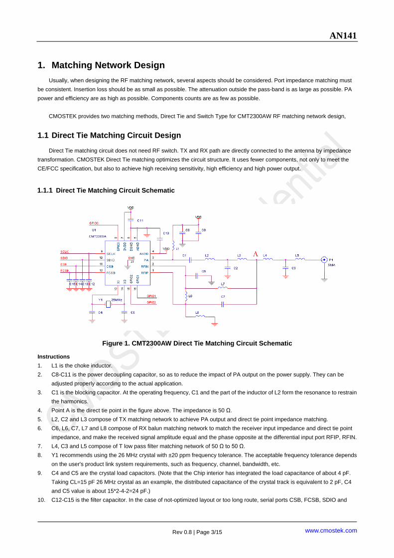
Figure 1. CMT2300AW Direct Tie Matching Circuit Schematic
Instructions
1. L1 is the choke inductor.
2. C8-C11 is the power decoupling capacitor, so as to reduce the impact of PA output on the power supply. They can be
adjusted properly according to the actual application.
3. C1 is the blocking capacitor. At the operating frequency, C1 and the part of the inductor of L2 form the resonance to restrain
the harmonics.
4. Point A is the direct tie point in the figure above. The impedance is 50 Ω.
5. L2, C2 and L3 compose of TX matching network to achieve PA output and direct tie point impedance matching.
6. C6, L6, C7, L7 and L8 compose of RX balun matching network to match the receiver input impedance and direct tie point
impedance, and make the received signal amplitude equal and the phase opposite at the differential input port RFIP, RFIN.
7. L4, C3 and L5 compose of T low pass filter matching network of 50 Ω to 50 Ω.
8. Y1 recommends using the 26 MHz crystal with ±20 ppm frequency tolerance. The acceptable frequency tolerance depends
on the user's product link system requirements, such as frequency, channel, bandwidth, etc.
9. C4 and C5 are the crystal load capacitors. (Note that the Chip interior has integrated the load capacitance of about 4 pF.
Taking CL=15 pF 26 MHz crystal as an example, the distributed capacitance of the crystal track is equivalent to 2 pF, C4
and C5 value is about 15*2-4-2=24 pF.)
10. C12-C15 is the filter capacitor. In the case of not-optimized layout or too long route, serial ports CSB, FCSB, SDIO and
AN141
Rev 0.8 | Page 4/15
www.cmostek.com
SCLK are easy to be disturbed. The bigger the power output (20 dBm) and the lower the operating frequency, the greater
the probability of interference. It is suggested that the capacitor (27 pF) connected to the ground is reserved near the four
pins to filter out the RF interference.
Component values of Direct Tie matching circuits in each frequency band are as below. The values for+13 dBm are shown
as table1. The values for +20 dBm are shown as table2.
Table 1. CMT2300AW Direct Tie BOM for +13dBm
No. Descriptions
Component values
Unit Supplier 433 MHz
+13 dBm
868 MHz
+13 dBm
915 MHz
+13 dBm
C1 ±5%, 0603 NP0, 50 V 15 22 22 pF
C2 ±5%, 0603 NP0, 50 V 5.6 6.2 6.2 pF
C3 ±5%, 0603 NP0, 50 V 7.5 3.6 3.3 pF
C4 ±5%, 0603 NP0, 50 V 24 24 24 pF
C5 ±5%, 0603 NP0, 50 V 24 24 24 pF
C6 ±5%, 0603 NP0, 50 V 4.7 2.2 2.2 pF
C7 ±5%, 0603 NP0, 50 V 4.7 2.2 2.2 pF
C8 ±5%, 0603 NP0, 50 V 4.7
4.7
4.7
4.7
uF
C9 ±5%, 0603 NP0, 50 V 470
470
470
470
pF
C10 ±5%, 0603 NP0, 50 V 0.1
0.1
0.1
0.1
uF
C11 ±5%, 0603 NP0, 50 V 0.1
0.1
0.1
0.1
uF
L1 ±5%, 0603multilayer chip inductor 180 100 100 nH Sunlord
L2 ±5%, 0603 multilayer chip inductor 56 10 8.2 nH Sunlord
L3 ±5%, 0603 multilayer chip inductor 39 8.2 6.8 nH Sunlord
L4 ±5%, 0603 multilayer chip inductor 18 10 8.2 nH Sunlord
L5 ±5%, 0603 multilayer chip inductor 18 10 8.2 nH Sunlord
L6 ±5%, 0603 multilayer chip inductor 27 15 12 nH Sunlord
L7 ±5%, 0603 multilayer chip inductor 27 15 12 nH Sunlord
L8 ±5%, 0603 multilayer chip inductor 68 12 12 nH Sunlord
Y1 ±10 ppm, SMD32*25 mm 26 MHz EPSON
U1 CMT2300AW, Ultra Low Power Sub-1GHz RF
Transceiver - - CMOSTEK
AN141
Rev 0.8 | Page 5/15
www.cmostek.com
Table 2. CMT2300AW Direct Tie BOM for +20dBm
No. Descriptions
Component values
Unit Supplier 433 MHz
+20dBm
868 MHz
+20dBm
915 MHz
+20 dBm
C1 ±5%, 0603 NP0, 50 V 15 18 18 pF
C2 ±5%, 0603 NP0, 50 V 3 3.6 3.6 pF
C3 ±5%, 0603 NP0, 50 V 6.2 3.3 3.3 pF
C4 ±5%, 0402 NP0, 50 V 24 24 24 pF
C5 ±5%, 0402 NP0, 50 V 24 24 24 pF
C6 ±5%, 0603 NP0, 50 V 4.7 2 1.8 pF
C7 ±5%, 0603 NP0, 50 V 4.7 2 1.8 pF
C8 ±5%, 0603 NP0, 50 V 4.7
4.7
4.7
4.7
uF
C9 ±5%, 0603 NP0, 50 V 470
470
470
470
pF
C10 ±5%, 0603 NP0, 50 V 0.1
0.1
0.1
0.1
uF
C11 ±5%, 0603 NP0, 50 V 0.1
0.1
0.1
0.1
uF
C12 ±5%, 0402 NP0, 50 V 27 pF
C13 ±5%, 0402 NP0, 50 V 27 pF
C14 ±5%, 0402 NP0, 50 V 27 pF
C15 ±5%, 0402 NP0, 50 V 27 pF
L1 ±5%, 0603 multilayer chip inductor 180 100 100 nH Sunlord
L2 ±5%, 0603 multilayer chip inductor 22 12 12 nH Sunlord
L3 ±5%, 0603 multilayer chip inductor 15 pF 15 15 nH Sunlord
L4 ±5%, 0603 multilayer chip inductor 33 6.2 6.2 nH Sunlord
L5 ±5%, 0603 multilayer chip inductor 33 6.2 6.2 nH Sunlord
L6 ±5%, 0603 multilayer chip inductor 27 15 15 nH Sunlord
L7 ±5%, 0603 multilayer chip inductor 27 15 15 nH Sunlord
L8 ±5%, 0603 multilayer chip inductor 68 12 12 nH Sunlord
Y1 ±10 ppm, SMD32*25 mm 26 MHz EPSON
U1 CMT2300AW, Ultra Low Power Sub-1GHz RF
Transceiver - - CMOSTEK
It is recommended that the users refer to CMOSTEK Direct Tie matching design. The network between TX and RX to Direct
Tie point uses the same value component as Table1 or Table2. The antenna matching filter network (L4, C3 and L5) needs to
adjust the order of the filter and component values according to the antenna impedance, cost requirements, whether to meet the
requirements of the CE/FCC specification and other factors. If the board area is limited, it is recommended that L1-L8 use the
high Q multilayer 0603 inductors (such as Sunlord SDCL1608 Series), but the capacitor can be used in the 0402 package.
AN141
Rev 0.8 | Page 6/15
www.cmostek.com
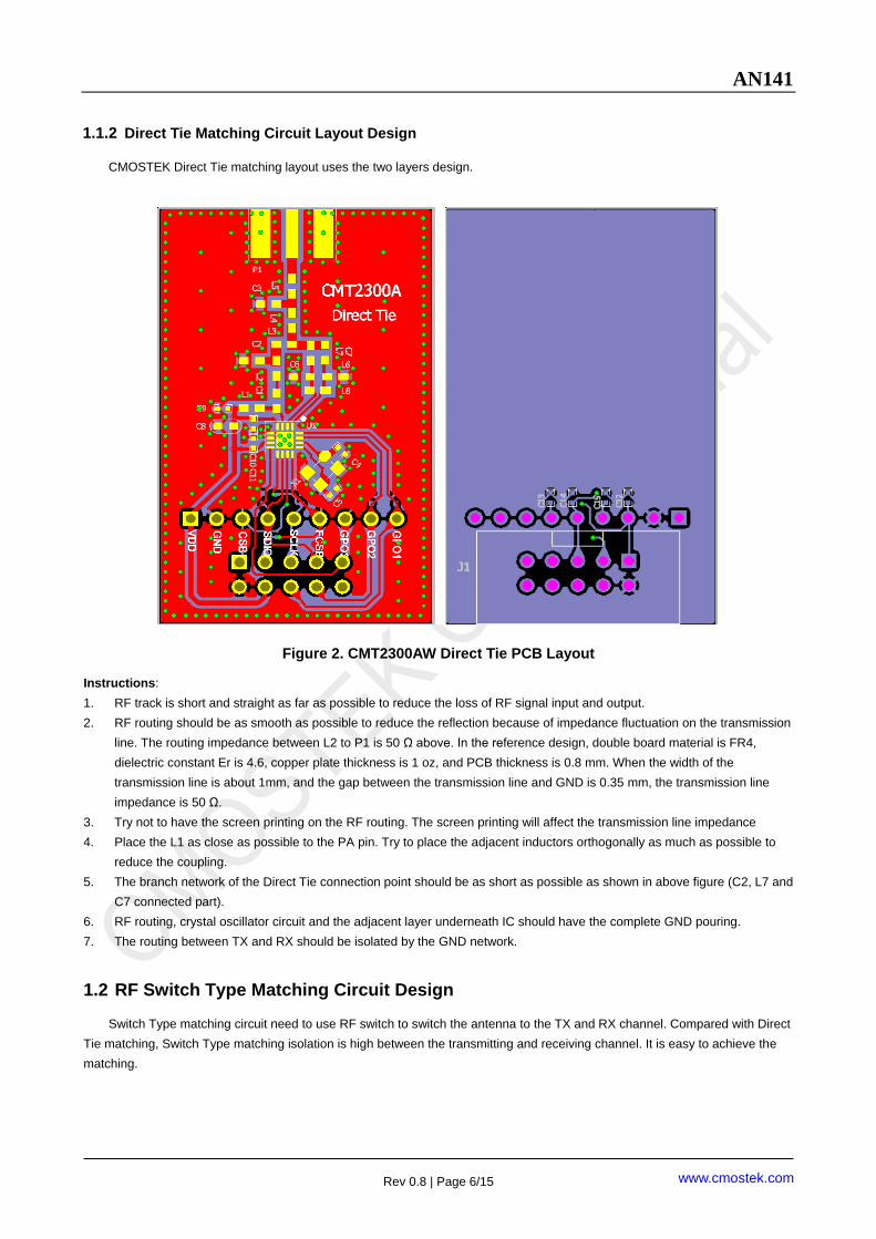
1.1.2 Direct Tie Matching Circuit Layout Design
CMOSTEK Direct Tie matching layout uses the two layers design.
Figure 2. CMT2300AW Direct Tie PCB Layout
Instructions:
1. RF track is short and straight as far as possible to reduce the loss of RF signal input and output.
2. RF routing should be as smooth as possible to reduce the reflection because of impedance fluctuation on the transmission
line. The routing impedance between L2 to P1 is 50 Ω above. In the reference design, double board material is FR4,
dielectric constant Er is 4.6, copper plate thickness is 1 oz, and PCB thickness is 0.8 mm. When the width of the
transmission line is about 1mm, and the gap between the transmission line and GND is 0.35 mm, the transmission line
impedance is 50 Ω.
3. Try not to have the screen printing on the RF routing. The screen printing will affect the transmission line impedance
4. Place the L1 as close as possible to the PA pin. Try to place the adjacent inductors orthogonally as much as possible to
reduce the coupling.
5. The branch network of the Direct Tie connection point should be as short as possible as shown in above figure (C2, L7 and
C7 connected part).
6. RF routing, crystal oscillator circuit and the adjacent layer underneath IC should have the complete GND pouring.
7. The routing between TX and RX should be isolated by the GND network.
1.2 RF Switch Type Matching Circuit Design
Switch Type matching circuit need to use RF switch to switch the antenna to the TX and RX channel. Compared with Direct
Tie matching, Switch Type matching isolation is high between the transmitting and receiving channel. It is easy to achieve the
matching.
AN141
Rev 0.8 | Page 7/15
www.cmostek.com
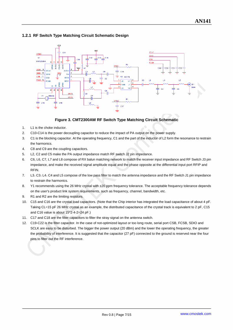
1.2.1 RF Switch Type Matching Circuit Schematic Design
Figure 3. CMT2300AW RF Switch Type Matching Circuit Schematic
1. L1 is the choke inductor.
2. C10-C14 is the power decoupling capacitor to reduce the impact of PA output on the power supply.
3. C1 is the blocking capacitor. At the operating frequency, C1 and the part of the inductor of L2 form the resonance to restrain
the harmonics.
4. C8 and C9 are the coupling capacitors.
5. L2, C2 and C5 make the PA output impedance match RF switch J2 pin impedance.
6. C6, L6, C7, L7 and L8 compose of RX balun matching network to match the receiver input impedance and RF Switch J3 pin
impedance, and make the received signal amplitude equal and the phase opposite at the differential input port RFIP and
RFIN.
7. L3,C3,L4,C4 and L5 compose of the low pass filter to match the antenna impedance and the RF Switch J1 pin impedance
to restrain the harmonics.
8. Y1 recommends using the 26 MHz crystal with ±20 ppm frequency tolerance. The acceptable frequency tolerance depends
on the user's product link system requirements, such as frequency, channel, bandwidth, etc.
9. R1 and R2 are the limiting resistors.
10. C15 and C16 are the crystal load capacitors. (Note that the Chip interior has integrated the load capacitance of about 4 pF.
Taking CL=15 pF 26 MHz crystal as an example, the distributed capacitance of the crystal track is equivalent to 2 pF, C15
and C16 value is about 15*2-4-2=24 pF.)
11. C17 and C18 are the filter capacitors to filter the stray signal on the antenna switch.
12. C19-C22 is the filter capacitor. In the case of not-optimized layout or too long route, serial port CSB, FCSB, SDIO and
SCLK are easy to be disturbed. The bigger the power output (20 dBm) and the lower the operating frequency, the greater
the probability of interference. It is suggested that the capacitor (27 pF) connected to the ground is reserved near the four
pins to filter out the RF interference.
AN141
Rev 0.8 | Page 8/15
www.cmostek.com
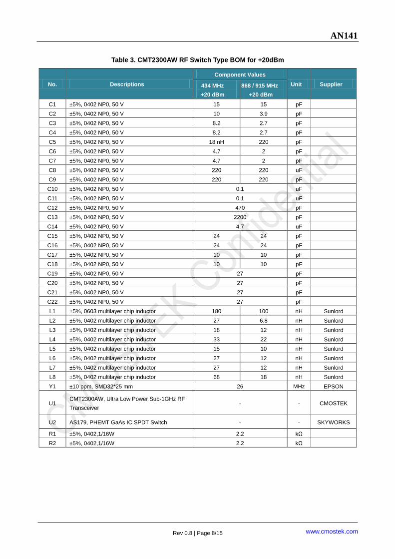
Table 3. CMT2300AW RF Switch Type BOM for +20dBm
No. Descriptions
Component Values
Unit Supplier 434 MHz
+20 dBm
868 / 915 MHz
+20 dBm
C1 ±5%, 0402 NP0, 50 V 15 15 pF
C2 ±5%, 0402 NP0, 50 V 10 3.9 pF
C3 ±5%, 0402 NP0, 50 V 8.2 2.7 pF
C4 ±5%, 0402 NP0, 50 V 8.2 2.7 pF
C5 ±5%, 0402 NP0, 50 V 18 nH 220 pF
C6 ±5%, 0402 NP0, 50 V 4.7 2 pF
C7 ±5%, 0402 NP0, 50 V 4.7 2 pF
C8 ±5%, 0402 NP0, 50 V 220 220 uF
C9 ±5%, 0402 NP0, 50 V 220 220 pF
C10 ±5%, 0402 NP0, 50 V 0.1
0.1
uF
C11 ±5%, 0402 NP0, 50 V 0.1
0.1
uF
C12 ±5%, 0402 NP0, 50 V 470
470
pF
C13 ±5%, 0402 NP0, 50 V 2200
2200
pF
C14 ±5%, 0402 NP0, 50 V 4.7
4.7
uF
C15 ±5%, 0402 NP0, 50 V 24 24 pF
C16 ±5%, 0402 NP0, 50 V 24 24 pF
C17 ±5%, 0402 NP0, 50 V 10 10 pF
C18 ±5%, 0402 NP0, 50 V 10 10 pF
C19 ±5%, 0402 NP0, 50 V 27 pF
C20 ±5%, 0402 NP0, 50 V 27 pF
C21 ±5%, 0402 NP0, 50 V 27 pF
C22 ±5%, 0402 NP0, 50 V 27 pF
L1 ±5%, 0603 multilayer chip inductor 180 100 nH Sunlord
L2 ±5%, 0402 multilayer chip inductor 27 6.8 nH Sunlord
L3 ±5%, 0402 multilayer chip inductor 18 12 nH Sunlord
L4 ±5%, 0402 multilayer chip inductor 33 22 nH Sunlord
L5 ±5%, 0402 multilayer chip inductor 15 10 nH Sunlord
L6 ±5%, 0402 multilayer chip inductor 27 12 nH Sunlord
L7 ±5%, 0402 multilayer chip inductor 27 12 nH Sunlord
L8 ±5%, 0402 multilayer chip inductor 68 18 nH Sunlord
Y1 ±10 ppm, SMD32*25 mm 26 MHz EPSON
U1 CMT2300AW, Ultra Low Power Sub-1GHz RF
Transceiver - - CMOSTEK
U2 AS179, PHEMT GaAs IC SPDT Switch - - SKYWORKS
R1 ±5%, 0402,1/16W 2.2 kΩ
R2 ±5%, 0402,1/16W 2.2 kΩ
AN141
Rev 0.8 | Page 9/15
www.cmostek.com
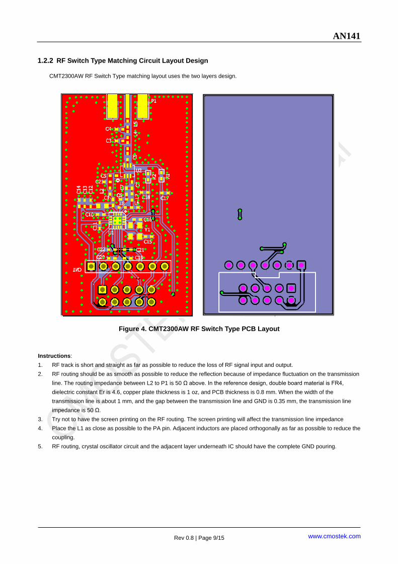
1.2.2 RF Switch Type Matching Circuit Layout Design
CMT2300AW RF Switch Type matching layout uses the two layers design.
Figure 4. CMT2300AW RF Switch Type PCB Layout
Instructions:
1. RF track is short and straight as far as possible to reduce the loss of RF signal input and output.
2. RF routing should be as smooth as possible to reduce the reflection because of impedance fluctuation on the transmission
line. The routing impedance between L2 to P1 is 50 Ω above. In the reference design, double board material is FR4,
dielectric constant Er is 4.6, copper plate thickness is 1 oz, and PCB thickness is 0.8 mm. When the width of the
transmission line is about 1 mm, and the gap between the transmission line and GND is 0.35 mm, the transmission line
impedance is 50 Ω.
3. Try not to have the screen printing on the RF routing. The screen printing will affect the transmission line impedance
4. Place the L1 as close as possible to the PA pin. Adjacent inductors are placed orthogonally as far as possible to reduce the
coupling.
5. RF routing, crystal oscillator circuit and the adjacent layer underneath IC should have the complete GND pouring.
AN141
Rev 0.8 | Page 10/15
www.cmostek.com
2. Crystal Circuit Design
Recommend using the following crystal specifications:
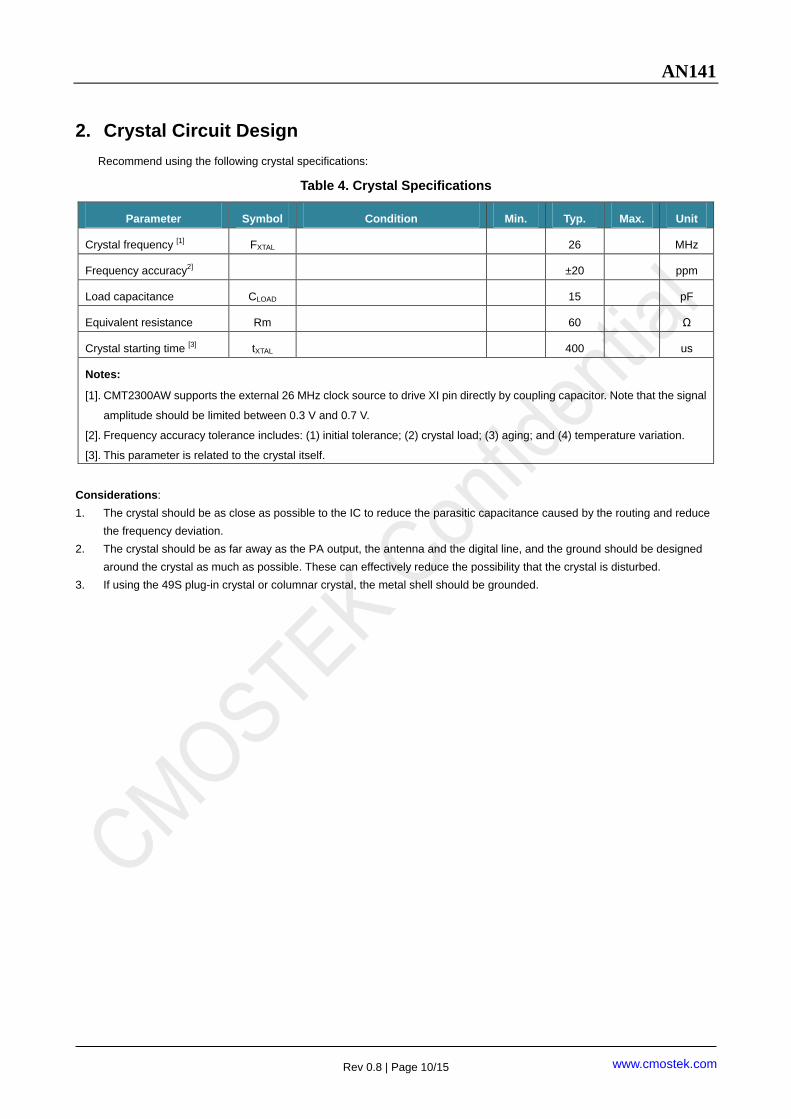
Table 4. Crystal Specifications
Parameter Symbol Condition Min. Typ. Max. Unit
Crystal frequency [1]
FXTAL 26 MHz
Frequency accuracy2]
±20 ppm
Load capacitance CLOAD 15 pF
Equivalent resistance Rm 60 Ω
Crystal starting time [3]
tXTAL 400 us
Notes:
[1]. CMT2300AW supports the external 26 MHz clock source to drive XI pin directly by coupling capacitor. Note that the signal
amplitude should be limited between 0.3 V and 0.7 V.
[2]. Frequency accuracy tolerance includes: (1) initial tolerance; (2) crystal load; (3) aging; and (4) temperature variation.
[3]. This parameter is related to the crystal itself.
Considerations:
1. The crystal should be as close as possible to the IC to reduce the parasitic capacitance caused by the routing and reduce
the frequency deviation.
2. The crystal should be as far away as the PA output, the antenna and the digital line, and the ground should be designed
around the crystal as much as possible. These can effectively reduce the possibility that the crystal is disturbed.
3. If using the 49S plug-in crystal or columnar crystal, the metal shell should be grounded.
AN141
Rev 0.8 | Page 11/15
www.cmostek.com
3. Digital Signal Design
Digital signal (including serial port and GPIO port) routing considerations are as follows:
1. The digital signal should be as far away from the crystal and RF routing.
2. The digital signal should be surrounded by ground pouring as far as possible to reduce the crosstalk with each other.
3. In the case of not-optimized layout or too long route, serial port CSB, FCSB, SDIO and SCLK are easy to be disturbed. The
bigger the power output (20 dBm) and the lower the operating frequency, the greater the probability of interference.
AN141
Rev 0.8 | Page 12/15
www.cmostek.com
4. Power and Ground Design
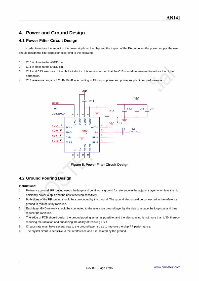
4.1 Power Filter Circuit Design
In order to reduce the impact of the power ripple on the chip and the impact of the PA output on the power supply, the user
should design the filter capacitor according to the following.
1. C10 is close to the AVDD pin
2. C11 is close to the DVDD pin.
3. C12 and C13 are close to the choke inductor. It is recommended that the C13 should be reserved to reduce the higher
harmonics.
4. C14 reference range is 4.7 uF- 10 uF in according to PA output power and power supply circuit performance.
Figure 5. Power Filter Circuit Design
4.2 Ground Pouring Design
Instructions:
1. Reference ground: RF routing needs the large and continuous ground for reference in the adjacent layer to achieve the high
efficiency power output and the best receiving sensitivity.
2. Both sides of the RF routing should be surrounded by the ground. The ground vias should be connected to the reference
ground to reduce stray radiation.
3. Each layer GND network should be connected to the reference ground layer by the vias to reduce the loop size and thus
reduce the radiation.
4. The edge of PCB should design the ground pouring as far as possible, and the vias spacing is not more than λ/10, thereby
reducing the radiation and enhancing the ability of resisting ESD.
5. IC substrate must have several vias to the ground layer, so as to improve the chip RF performance.
6. The crystal circuit is sensitive to the interference and it is isolated by the ground.
AN141
Rev 0.8 | Page 13/15
www.cmostek.com
5. Design Checklist
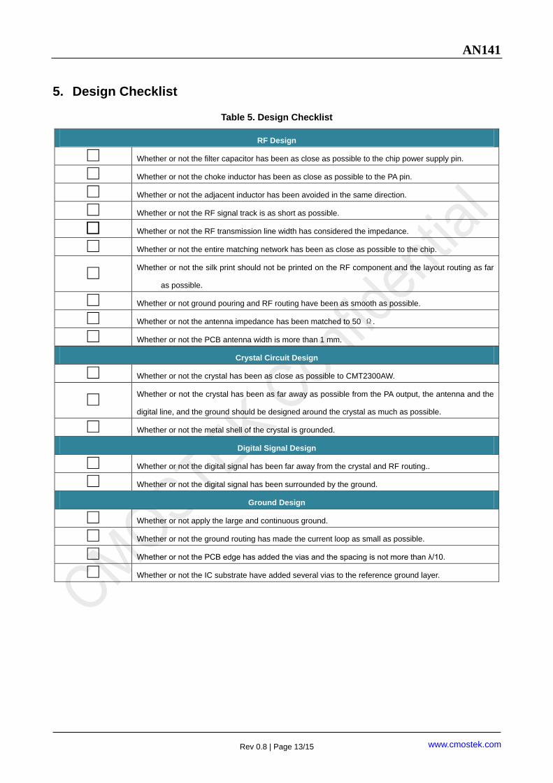
Table 5. Design Checklist
RF Design
□ Whether or not the filter capacitor has been as close as possible to the chip power supply pin.
□ Whether or not the choke inductor has been as close as possible to the PA pin.
□ Whether or not the adjacent inductor has been avoided in the same direction.
□ Whether or not the RF signal track is as short as possible.
□ Whether or not the RF transmission line width has considered the impedance.
□ Whether or not the entire matching network has been as close as possible to the chip.
□ Whether or not the silk print should not be printed on the RF component and the layout routing as far
as possible.
□ Whether or not ground pouring and RF routing have been as smooth as possible.
□ Whether or not the antenna impedance has been matched to 50 Ω.
□ Whether or not the PCB antenna width is more than 1 mm.
Crystal Circuit Design
□ Whether or not the crystal has been as close as possible to CMT2300AW.
□ Whether or not the crystal has been as far away as possible from the PA output, the antenna and the
digital line, and the ground should be designed around the crystal as much as possible.
□ Whether or not the metal shell of the crystal is grounded.
Digital Signal Design
□ Whether or not the digital signal has been far away from the crystal and RF routing..
□ Whether or not the digital signal has been surrounded by the ground.
Ground Design
□ Whether or not apply the large and continuous ground.
□ Whether or not the ground routing has made the current loop as small as possible.
□ Whether or not the PCB edge has added the vias and the spacing is not more than λ/10.
□ Whether or not the IC substrate have added several vias to the reference ground layer.
AN141
Rev 0.8 | Page 14/15
www.cmostek.com
6. Document Change List
Table 6. Document Change List
Rev. No. Chapter Description of Changes Date
0.8 All Initial release 2017-05-05
AN141
Rev 0.8 | Page 15/15
www.cmostek.com
7. Contact Information CMOSTEK Microelectronics Co., Ltd.
Room 203, Honghai Building, Qianhai Road. Nanshan District
Shenzhen, Guangdong, China PRC
Zip Code: 518000
Tel: 0755 - 83235017
Fax: 0755 - 82761326
Sales: [email protected]
Technical support: [email protected]
Website: www.cmostek.com
The information furnished by CMOSTEK is believed to be accurate and reliable. However, no responsibility is assumed for
inaccuracies and specifications within this document are subject to change without notice. The material contained herein is
the exclusive property of CMOSTEK and shall not be distributed, reproduced, or disclosed in whole or in part without prior
written permission of CMOSTEK. CMOSTEK products are not authorized for use as critical components in life support
devices or systems without express written approval of CMOSTEK. The CMOSTEK logo is a registered trademark of
CMOSTEK Microelectronics Co., Ltd. All other names are the property of their respective owners.
Copyright. CMOSTEK Microelectronics Co., Ltd. All rights are reserved.