Embed Size (px)
Citation preview

1
University Politehnica Bucharest Computers Faculty
CN Project : Verilog implementation of MIPS processor
Coordinator :Decebal Popescu, Teaching Assistant, Ph.D
Students : Cocorada Sorin Comanescu George Manta Mihai Parpauta Alexandru Safta Octavian
2
SUMMARY
Project purpose…………………………………………………………………………..3
The projectio n phases …………………………………………………………………..3
MIPS instructions format ………………………………………………………………3
The logical transfers between registers ………………………….………………….…4
The set of instructions …………………………………………………………………..5 The instructions read unit……………………………………………………………….6 Logical operations with Immediate……………………………………………………..7 Load operation…..…………………………………………………...…………………..7 Store and Branch operations……………………………………………………………9 Project of the command unit…………………………………………………………...11 Concept of local decodification………………………………………………………...12 The command bloc for the UAL……………………………………………………….15 The logic for the main command………………………………………………………16 MIPS processor bloc scheme …………………………………………………………..18 The main problems of the single clock cycle processor ……………………………...19 The command general syntax …………………………………………………………19 Test program…………………………………………………………………………....20 Bibliography…………………………………………………………………………….21
3
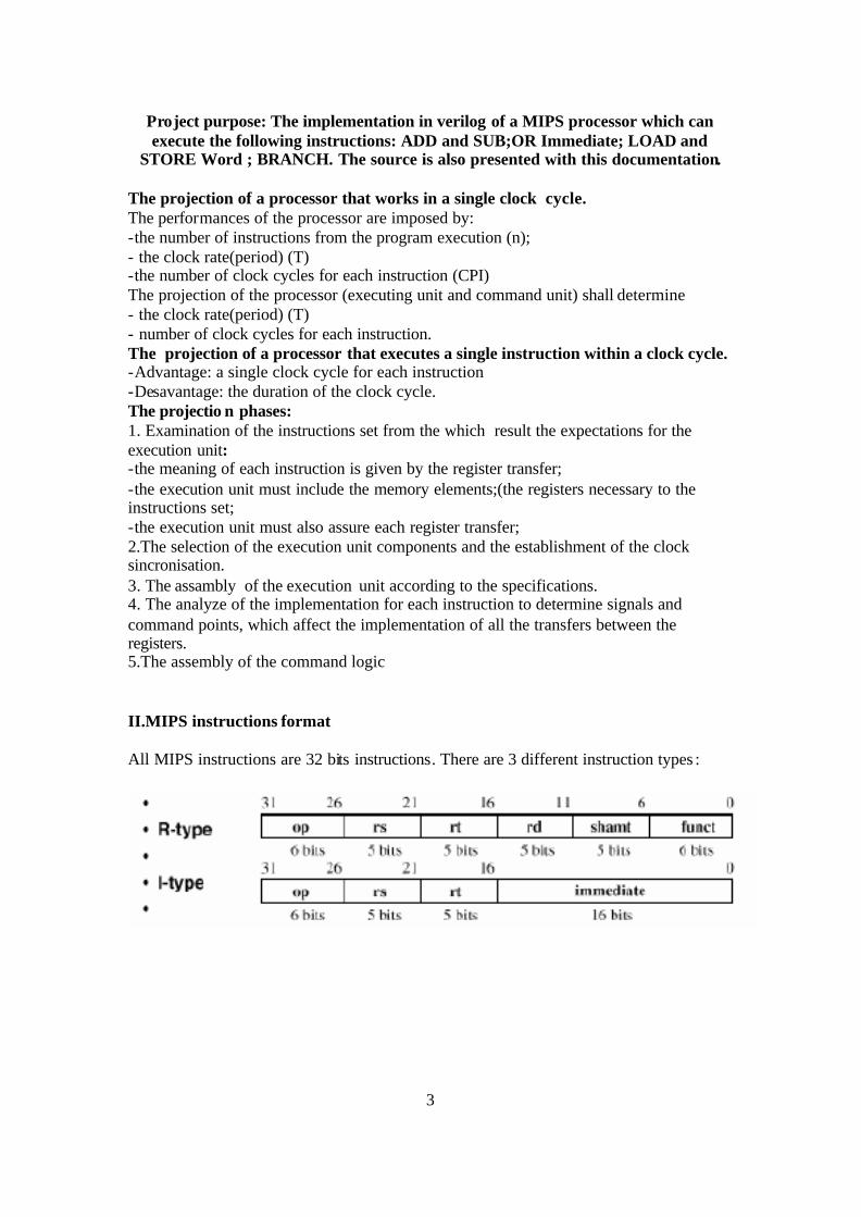
Project purpose: The implementation in verilog of a MIPS processor which can execute the following instructions: ADD and SUB;OR Immediate; LOAD and
STORE Word ; BRANCH. The source is also presented with this documentation. The projection of a processor that works in a single clock cycle. The performances of the processor are imposed by: -the number of instructions from the program execution (n); - the clock rate(period) (T) -the number of clock cycles for each instruction (CPI) The projection of the processor (executing unit and command unit) shall determine - the clock rate(period) (T) - number of clock cycles for each instruction. The projection of a processor that executes a single instruction within a clock cycle. -Advantage: a single clock cycle for each instruction -Desavantage: the duration of the clock cycle. The projectio n phases: 1. Examination of the instructions set from the which result the expectations for the execution unit: -the meaning of each instruction is given by the register transfer; -the execution unit must include the memory elements;(the registers necessary to the instructions set; -the execution unit must also assure each register transfer; 2.The selection of the execution unit components and the establishment of the clock sincronisation. 3. The assambly of the execution unit according to the specifications. 4. The analyze of the implementation for each instruction to determine signals and command points, which affect the implementation of all the transfers between the registers. 5.The assembly of the command logic II.MIPS instructions format All MIPS instructions are 32 bits instructions. There are 3 different instruction types :
4
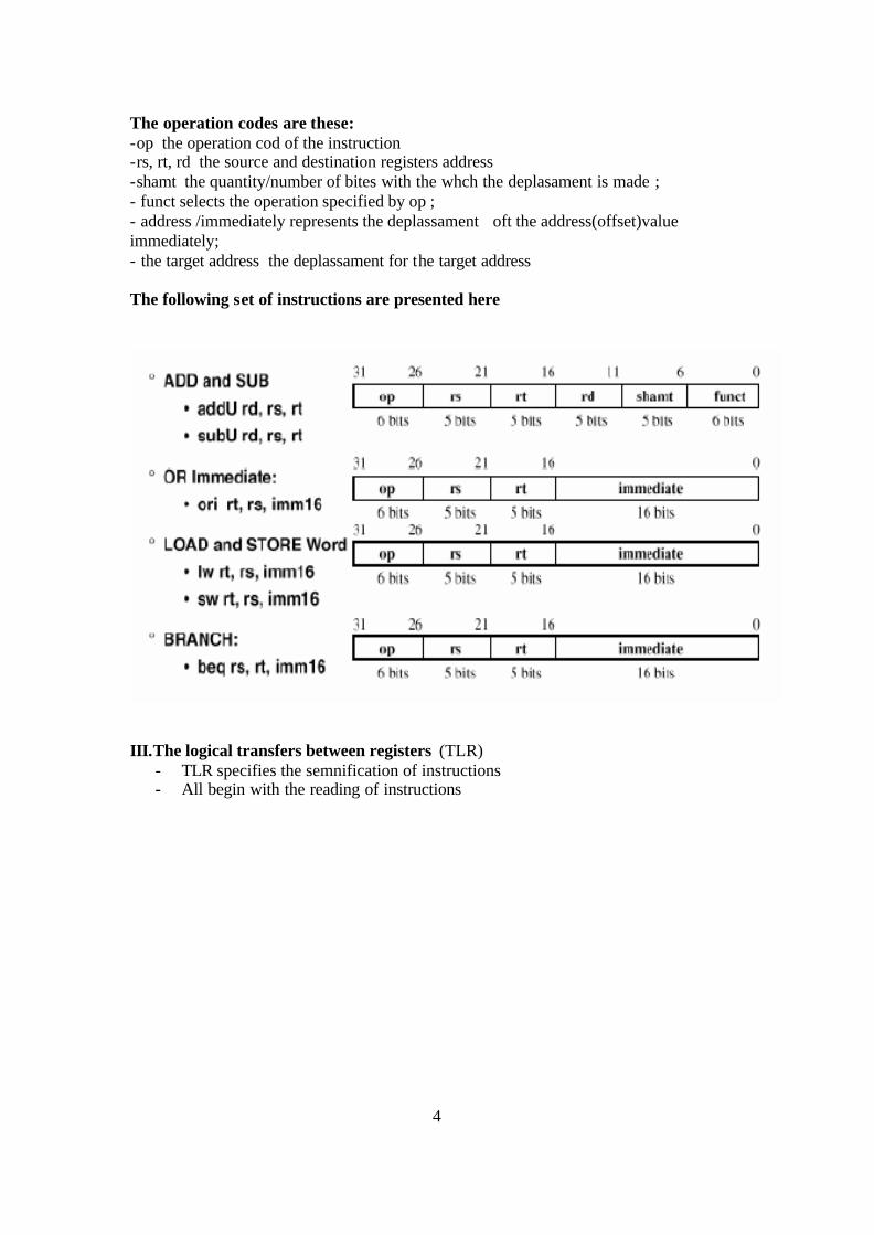
The operation codes are these: -op the operation cod of the instruction -rs, rt, rd the source and destination registers address -shamt the quantity/number of bites with the whch the deplasament is made ; - funct selects the operation specified by op ; - address /immediately represents the deplassament oft the address(offset)value immediately; - the target address the deplassament for the target address The following set of instructions are presented here
III.The logical transfers between registers (TLR)
- TLR specifies the semnification of instructions - All begin with the reading of instructions

5
1. The set of instructions : Memory : - instructions and data Registers: - capacity 32 words x 32 bits - read rs, rt; - write rd, rt. Counter program (PC) Signal extender circuit (Extender) Add/Remove register (offset-ul) extended Add 4 or Immediately extended to PC 2. The components of the execution unit: - Combinatory elements - Memory elements - Sincronisation methodology

6
The general registers : There are 32 registers biport (out) The register is selected by : -RA (number ) specifies the general registry which is placed on busA -RB (number ) specifies the general registry which is placed on busB -RW (number ) specifies the general registry which is placed on busW -CLK in is effective only to the writing The ideal memory : - Data In - Data Out
- The word in the meomory is selected using the following steps : - Address selects the word that will be forced on DataOut - Write Enable = 1is forced : the word from memory will be forced on DataOut. - CLK In - the CLK signal is used only on writing - During the reading operations the comportament of the bloc is unitary The sincronisation metodology (clocking) All the memory elements are controlled by the same clock front - the duration of the cycle equals CLK -> Q + Lo ngest delay + Setup Time + Clock Skew - CLK -> Q + shortest delay >Hold Time 3.The instructions read unit: The RTL operations are:
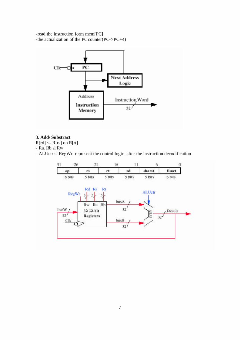
7
-read the instruction form mem[PC] -the actualization of the PC counter(PC->PC+4)
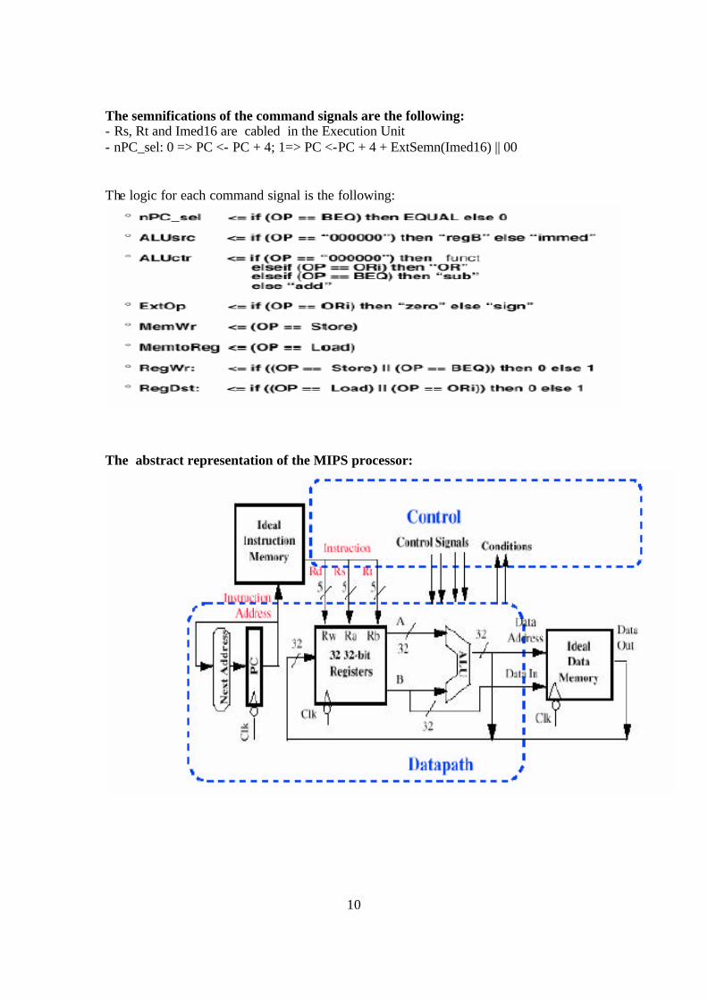
3. Add/ Substract R[rd] <- R[rs] op R[rt] - Ra. Rb si Rw - ALUctr si RegWr: represent the control logic after the instruction decodification

8
Logical operations with Immediate:
Load operations diagram

9
Store operations :
Branch operation:
beq rs, rt, imm16 - mem[PC] reads the instruction from memory - Egal <- R[rs] = = R[rt] Calculates the branch condition - if(COND = 0) Calculates the next instruction address - PC <- PC + 4 + (ExtSemn(imm16) x4) - else - PC <- PC + 4 The execution unit for branch command: - generates equal
10
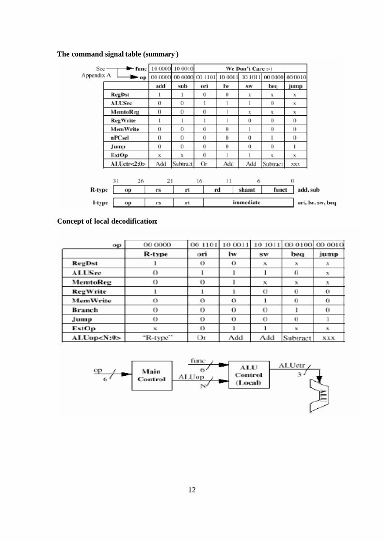
The semnifications of the command signals are the following: - Rs, Rt and Imed16 are cabled in the Execution Unit - nPC_sel: 0 => PC <- PC + 4; 1=> PC <-PC + 4 + ExtSemn(Imed16) || 00 The logic for each command signal is the following:
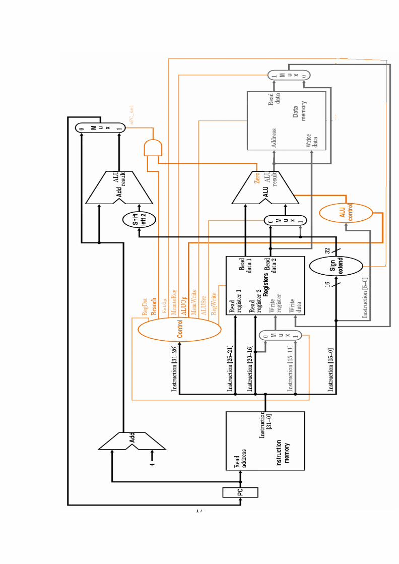
The abstract representation of the MIPS processor:

11
The MIPS structure is characterized by the following elements:
- the instructions have a fixed length - the source registers are positioned in the same fields - “immediately” has the same dimension and positioning - the operations are made with operands from the registers or from the registers
field The Execution Unit works inb a single cycle so CPI=1, and the duration of the cycle is very big . Project of the command unit;
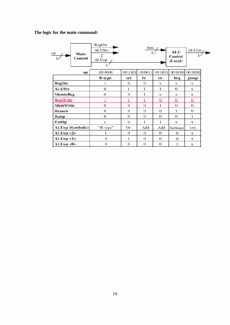
Summary of the command signals:
12
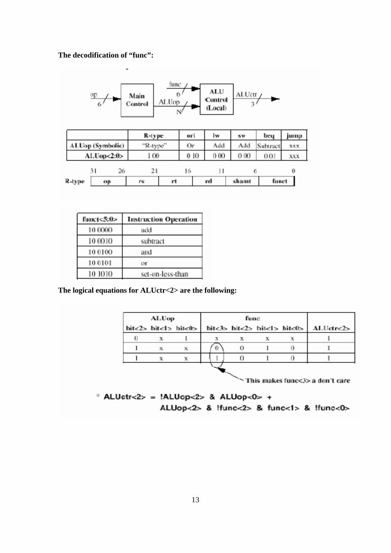
The command signal table (summary )
Concept of local decodification:
13
The decodification of “func”:
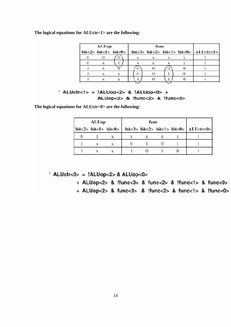
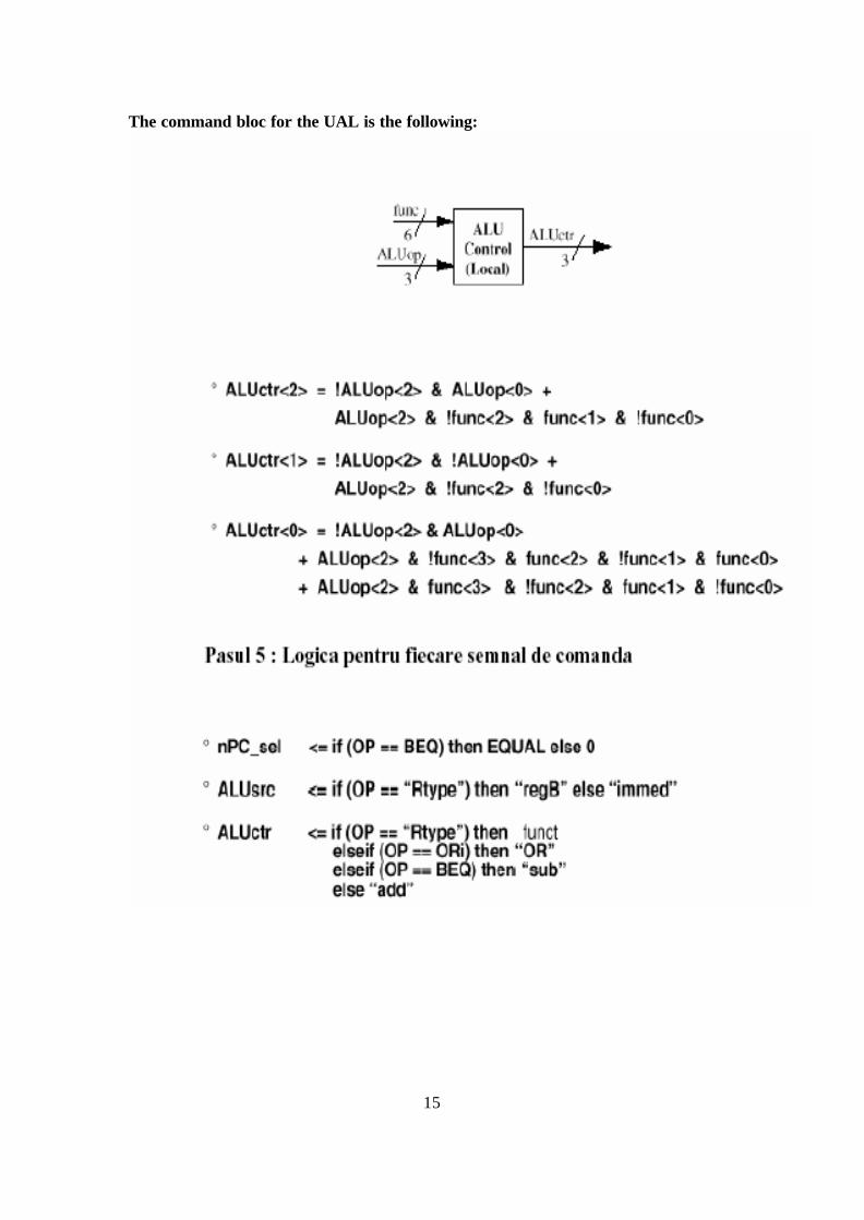
The logical equations for ALUctr<2> are the following:
14
The logical equations for ALUctr<1> are the following:
The logical equations for ALUctr<0> are the following:
15
The command bloc for the UAL is the following:
16
The logic for the main command:
17
18
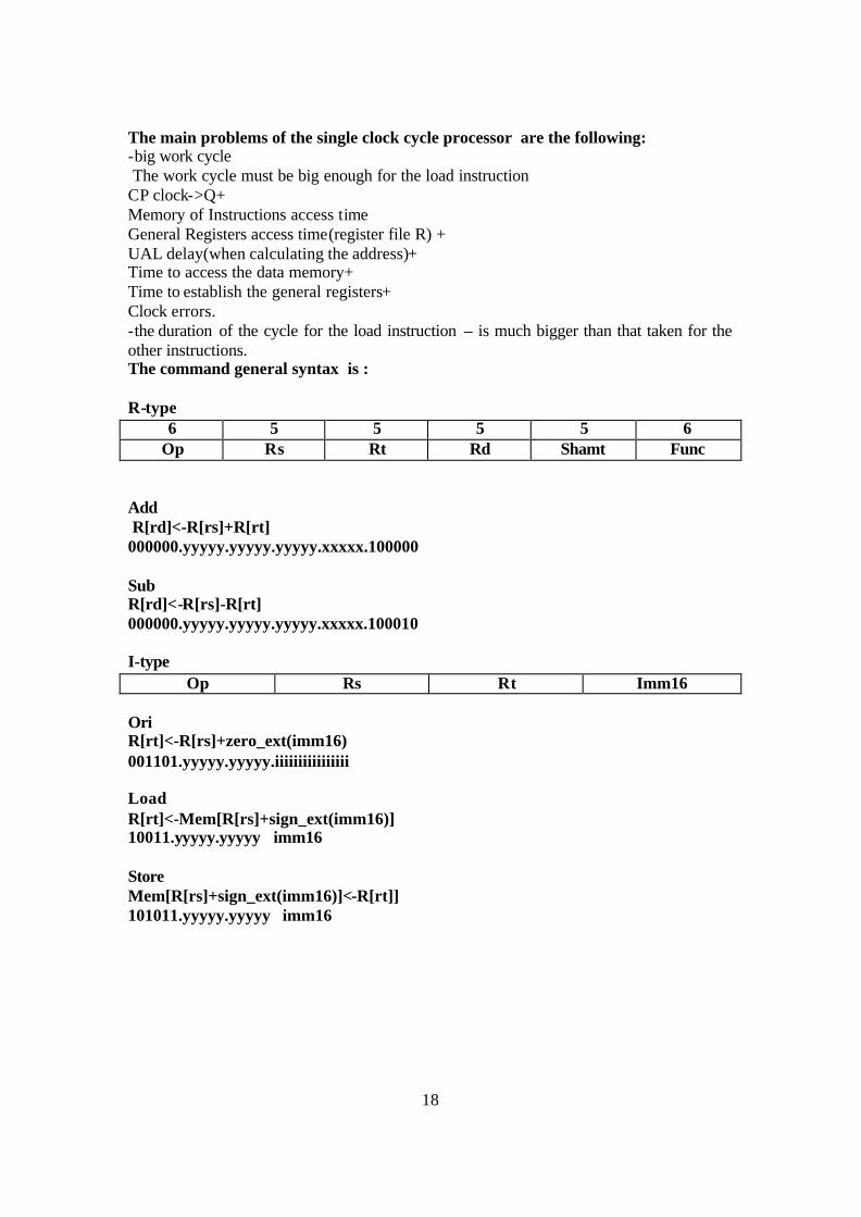
The main problems of the single clock cycle processor are the following: -big work cycle The work cycle must be big enough for the load instruction CP clock->Q+ Memory of Instructions access time General Registers access time(register file R) + UAL delay(when calculating the address)+ Time to access the data memory+ Time to establish the general registers+ Clock errors. -the duration of the cycle for the load instruction – is much bigger than that taken for the other instructions. The command general syntax is : R-type
6 5 5 5 5 6 Op Rs Rt Rd Shamt Func
Add R[rd]<-R[rs]+R[rt] 000000.yyyyy.yyyyy.yyyyy.xxxxx.100000 Sub R[rd]<-R[rs]-R[rt] 000000.yyyyy.yyyyy.yyyyy.xxxxx.100010 I-type
Op Rs Rt Imm16 Ori R[rt]<-R[rs]+zero_ext(imm16) 001101.yyyyy.yyyyy.iiiiiiiiiiiiiiii Load R[rt]<-Mem[R[rs]+sign_ext(imm16)] 10011.yyyyy.yyyyy imm16 Store Mem[R[rs]+sign_ext(imm16)]<-R[rt]] 101011.yyyyy.yyyyy imm16
19
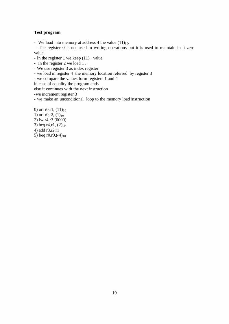
Test program - We load into memory at address 4 the value (11)10. - The register 0 is not used in writing operations but it is used to maintain in it zero value. - In the register 1 we keep (11)10 value. - In the register 2 we load 1 . - We use register 3 as index register - we load in register 4 the memory location referred by register 3 - we compare the values form registers 1 and 4 in case of equality the program ends else it continues with the next instruction -we increment register 3 - we make an unconditional loop to the memory load instruction 0) ori r0,r1, (11)10 1) ori r0,r2, (1)10 2) lw r4,r3 (0000) 3) beq r4,r1, (2)10 4) add r3,r2,r1 5) beq r0,r0,(-4)10

20
Bibliography CN Courses –Course 5 from the 2’nd semester
-Course 8 from the 1’st semester
On-line documentation : http://www.deeps.org http://www.csit -sun.pub.ro