Embed Size (px)
Citation preview
80 Cornell NanoScale Facility
Ele
ctro
nic
s
Vertical Tunneling Field Effect Transistors (Thin-TFETs) Based on BP/SnSe2 Heterostructure
CNF Project Number: 2324-15
Principal Investigator: Huili Grace Xing
Users: Hyunjea Lee, Xiang Li
Affiliation: School of Electrical and Computer Engineering, Cornell UniversityPrimary Source of Research Funding: LEAST project (Center for Low Energy Systems Technology)Contact: [email protected], [email protected], [email protected] CNF Tools Used: Autostop i-line stepper, carbon nanotube/graphene furnace, JEOL 6300,
AFM – Veeco Icon, AJA sputter deposition, SC4500 odd-hour evaporator, DISCO dicing saw
Abstract:
Two-dimensional materials with clean surface and layered structure have many advantages over three-dimensional counterparts to be used for steep tunneling devices. This work presents two-dimensional heterojunction interlayer tunneling field effect transistors (Thin-TFETs) using black phosphorus (BP)/SnSe2 heterostructure. Broken gap alignment (type III) between BP and SnSe2 offers a desirable condition for band to band tunneling, and a solid polymer electrolyte (PEO:CsClO4) is used to improve subthreshold swing. Graphite electrodes are used to protect air-sensitive BP surface, and most of processing is done in a glove box for the same reason. At room temperature in N2, the subthreshold swing of the representative device reaches 180 mV/dec for exceeding two decades of drain current, and the Ion/Ioff extends to more than three decades. This work helps the understanding of interband tunneling between layered materials, which forms the basis for low-power tunneling devices.
Summary of Research:
Two-dimensional materials with clean surfaces and layered structures have many advantages over three-dimensional counterparts to be used for steep tunneling devices. This work presents two-dimensional heterojunction interlayer tunneling field effect transistors (Thin-TFETs) using black phosphorus / tin selenide (BP/SnSe2) heterostructure. Broken gap alignment (type III) between BP and SnSe2 offers a desirable condition for band to band tunneling, and a solid polymer electrolyte (PEO:CsClO4) is used to improve subthreshold swing. Graphite electrodes are used to protect air-sensitive BP surface, and most of processing is done in a glove box for the same reason. At room temperature in N2, the subthreshold swing of the representative device reaches 180 mV/dec for exceeding two decades of drain current, and the Ion/Ioff extends to more than three decades.
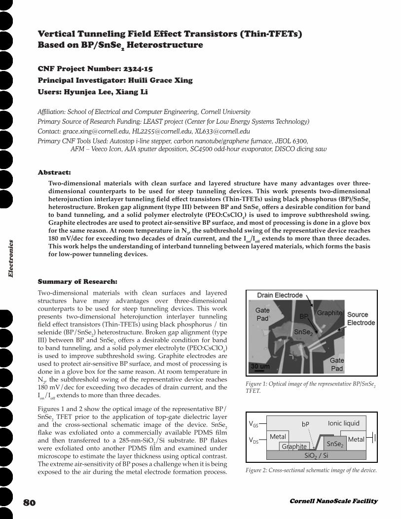
Figures 1 and 2 show the optical image of the representative BP/SnSe2 TFET prior to the application of top-gate dielectric layer and the cross-sectional schematic image of the device. SnSe2 flake was exfoliated onto a commercially available PDMS film and then transferred to a 285-nm-SiO2/Si substrate. BP flakes were exfoliated onto another PDMS film and examined under microscope to estimate the layer thickness using optical contrast. The extreme air-sensitivity of BP poses a challenge when it is being exposed to the air during the metal electrode formation process.
Figure 1: Optical image of the representative BP/SnSe2 TFET.
Figure 2: Cross-sectional schematic image of the device.
812017-2018 Research Accomplishments
Electron
ics
Semi-metallic graphite flakes were transferred on top of the BP flakes, which is used to make contacts with metal pads acting as a capping layer for BP. To minimize interfacial states resulting from interfacial damage or contamination, all the exfoliation processes were done in a glove box to protect air-sensitive BP and SnSe2 from being exposed to the air. The substrate was spin-coated with e-beam resist in the glove box and Cr/Au electrodes (5/50 nm) were formed by e-beam lithography followed by lift-off in the glove box. The solid polymer electrolyte, PEO:CsClO4, was deposited onto the substrate as a gate dielectric that also acts as a capping layer for BP and SnSe2. When dissolved in PEO, CsClO4 is ionized into Cs+ and ClO4-, forming electric double layers which react to voltage bias.
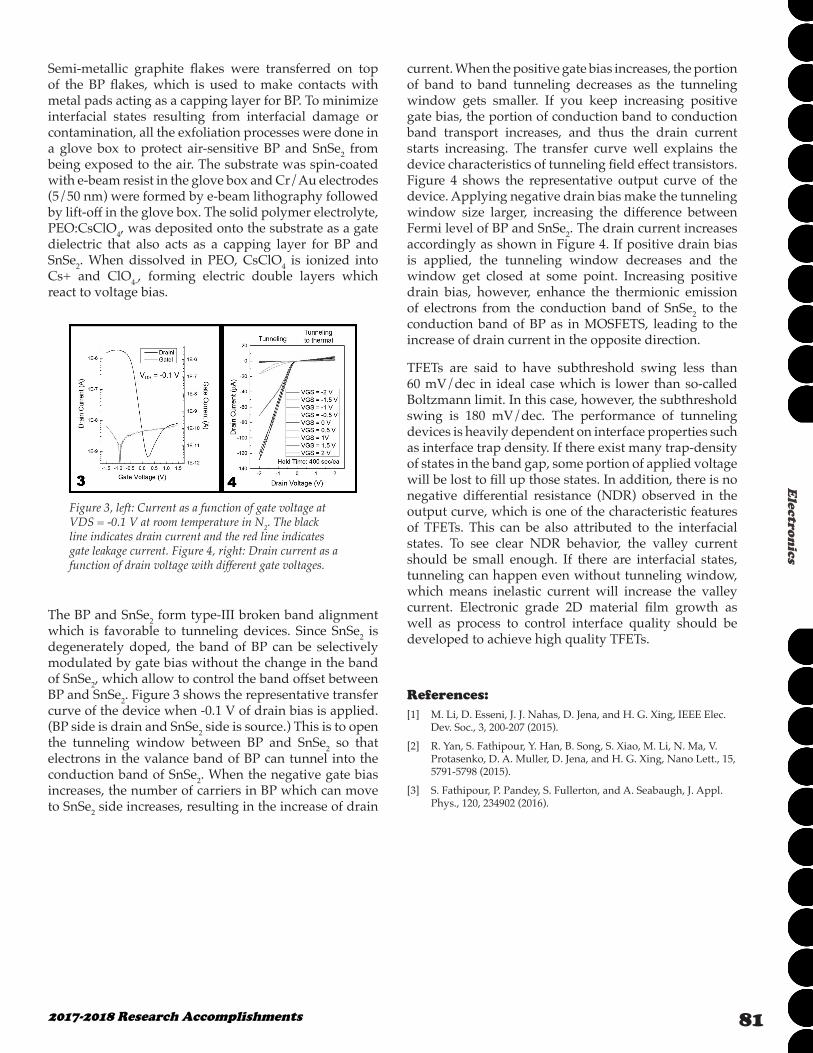
current. When the positive gate bias increases, the portion of band to band tunneling decreases as the tunneling window gets smaller. If you keep increasing positive gate bias, the portion of conduction band to conduction band transport increases, and thus the drain current starts increasing. The transfer curve well explains the device characteristics of tunneling field effect transistors. Figure 4 shows the representative output curve of the device. Applying negative drain bias make the tunneling window size larger, increasing the difference between Fermi level of BP and SnSe2. The drain current increases accordingly as shown in Figure 4. If positive drain bias is applied, the tunneling window decreases and the window get closed at some point. Increasing positive drain bias, however, enhance the thermionic emission of electrons from the conduction band of SnSe2 to the conduction band of BP as in MOSFETS, leading to the increase of drain current in the opposite direction.
TFETs are said to have subthreshold swing less than 60 mV/dec in ideal case which is lower than so-called Boltzmann limit. In this case, however, the subthreshold swing is 180 mV/dec. The performance of tunneling devices is heavily dependent on interface properties such as interface trap density. If there exist many trap-density of states in the band gap, some portion of applied voltage will be lost to fill up those states. In addition, there is no negative differential resistance (NDR) observed in the output curve, which is one of the characteristic features of TFETs. This can be also attributed to the interfacial states. To see clear NDR behavior, the valley current should be small enough. If there are interfacial states, tunneling can happen even without tunneling window, which means inelastic current will increase the valley current. Electronic grade 2D material film growth as well as process to control interface quality should be developed to achieve high quality TFETs.
References:[1] M. Li, D. Esseni, J. J. Nahas, D. Jena, and H. G. Xing, IEEE Elec.
Dev. Soc., 3, 200-207 (2015).
[2] R. Yan, S. Fathipour, Y. Han, B. Song, S. Xiao, M. Li, N. Ma, V. Protasenko, D. A. Muller, D. Jena, and H. G. Xing, Nano Lett., 15, 5791-5798 (2015).
[3] S. Fathipour, P. Pandey, S. Fullerton, and A. Seabaugh, J. Appl. Phys., 120, 234902 (2016).
Figure 3, left: Current as a function of gate voltage at VDS = -0.1 V at room temperature in N2. The black line indicates drain current and the red line indicates gate leakage current. Figure 4, right: Drain current as a function of drain voltage with different gate voltages.
The BP and SnSe2 form type-III broken band alignment which is favorable to tunneling devices. Since SnSe2 is degenerately doped, the band of BP can be selectively modulated by gate bias without the change in the band of SnSe2, which allow to control the band offset between BP and SnSe2. Figure 3 shows the representative transfer curve of the device when -0.1 V of drain bias is applied. (BP side is drain and SnSe2 side is source.) This is to open the tunneling window between BP and SnSe2 so that electrons in the valance band of BP can tunnel into the conduction band of SnSe2. When the negative gate bias increases, the number of carriers in BP which can move to SnSe2 side increases, resulting in the increase of drain
82 Cornell NanoScale Facility
Ele
ctro
nic
s
Self-Assembled Silica Nano-Spheres for Dual Metal Junction-Barrier-Schottky Diodes
CNF Project Number: 2350-15
Principal Investigators: Prof. Debdeep Jena, Prof. Huili Grace Xing
User: Jae Ho Shin
Affiliation: Department of Materials Science and Engineering, Cornell UniversityPrimary Source of Research Funding: SixpointsContact: [email protected], [email protected], [email protected]: djena.engineering.cornell.edu, grace.engineering.cornell.eduPrimary CNF Tools Used: ABM contact aligner, wet chemistry bench, Zeiss Supra/Ultra SEM, odd hour e-beam
evaporator, AJA sputter, PT-770 ICP RIE, photoresist spinner, hotplate, optical microscope
Abstract:
We report on a time and cost-effective method of selectively depositing thin metal films onto substrates. Silica nanospheres of 50 nm diameter were hexagonally packed using Triton X-100 surfactant on the DI water/air interface, and were transferred onto bulk n type gallium nitride substrates. After inspection using the scanning electron microscope, 20 nm thick metal was deposited on top. After stripping of the silica, a triangular shaped array of metal deposits remained. This technique will enable a quick, simple method of fabricating dual metal junction-barrier-Schottky-diodes, which use the difference in work function of two metals to reduce reverse leakage as in a p-n diode, as well as retain the low turn-on voltage of Schottky barrier diodes.
Summary of Research:
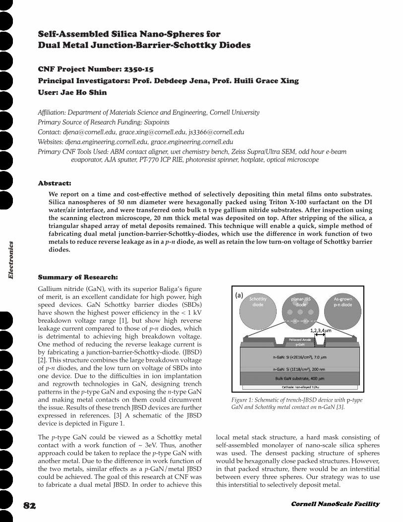
Figure 1: Schematic of trench-JBSD device with p-type GaN and Schottky metal contact on n-GaN [3].
Gallium nitride (GaN), with its superior Baliga’s figure of merit, is an excellent candidate for high power, high speed devices. GaN Schottky barrier diodes (SBDs) have shown the highest power efficiency in the < 1 kV breakdown voltage range [1], but show high reverse leakage current compared to those of p-n diodes, which is detrimental to achieving high breakdown voltage. One method of reducing the reverse leakage current is by fabricating a junction-barrier-Schottky-diode. (JBSD) [2]. This structure combines the large breakdown voltage of p-n diodes, and the low turn on voltage of SBDs into one device. Due to the difficulties in ion implantation and regrowth technologies in GaN, designing trench patterns in the p-type GaN and exposing the n-type GaN and making metal contacts on them could circumvent the issue. Results of these trench JBSD devices are further expressed in references. [3] A schematic of the JBSD device is depicted in Figure 1.
The p-type GaN could be viewed as a Schottky metal contact with a work function of ~ 3eV. Thus, another approach could be taken to replace the p-type GaN with another metal. Due to the difference in work function of the two metals, similar effects as a p-GaN/metal JBSD could be achieved. The goal of this research at CNF was to fabricate a dual metal JBSD. In order to achieve this
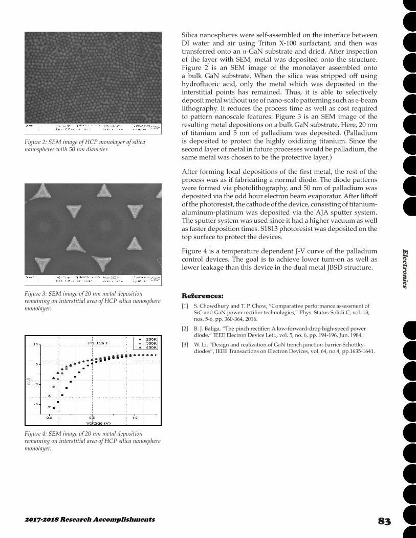
local metal stack structure, a hard mask consisting of self-assembled monolayer of nano-scale silica spheres was used. The densest packing structure of spheres would be hexagonally close packed structures. However, in that packed structure, there would be an interstitial between every three spheres. Our strategy was to use this interstitial to selectively deposit metal.
832017-2018 Research Accomplishments
Electron
ics
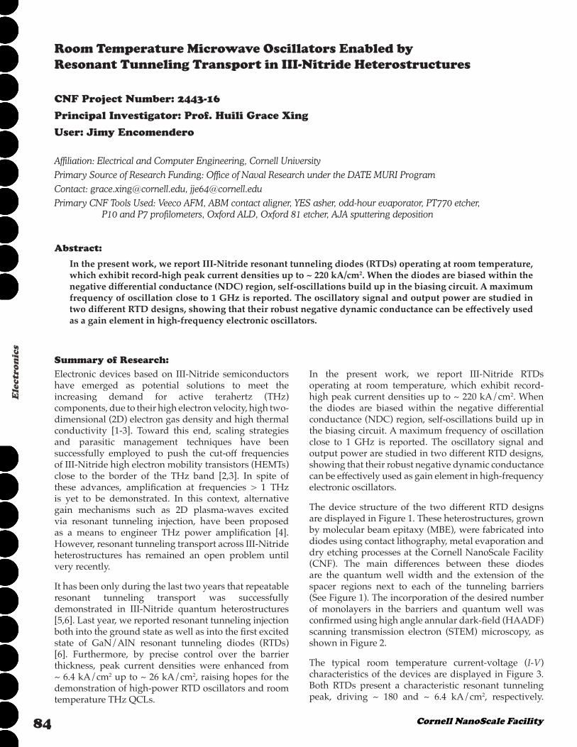
Silica nanospheres were self-assembled on the interface between DI water and air using Triton X-100 surfactant, and then was transferred onto an n-GaN substrate and dried. After inspection of the layer with SEM, metal was deposited onto the structure. Figure 2 is an SEM image of the monolayer assembled onto a bulk GaN substrate. When the silica was stripped off using hydrofluoric acid, only the metal which was deposited in the interstitial points has remained. Thus, it is able to selectively deposit metal without use of nano-scale patterning such as e-beam lithography. It reduces the process time as well as cost required to pattern nanoscale features. Figure 3 is an SEM image of the resulting metal depositions on a bulk GaN substrate. Here, 20 nm of titanium and 5 nm of palladium was deposited. (Palladium is deposited to protect the highly oxidizing titanium. Since the second layer of metal in future processes would be palladium, the same metal was chosen to be the protective layer.)
After forming local depositions of the first metal, the rest of the process was as if fabricating a normal diode. The diode patterns were formed via photolithography, and 50 nm of palladium was deposited via the odd hour electron beam evaporator. After liftoff of the photoresist, the cathode of the device, consisting of titanium-aluminum-platinum was deposited via the AJA sputter system. The sputter system was used since it had a higher vacuum as well as faster deposition times. S1813 photoresist was deposited on the top surface to protect the devices.
Figure 4 is a temperature dependent J-V curve of the palladium control devices. The goal is to achieve lower turn-on as well as lower leakage than this device in the dual metal JBSD structure.
References:[1] S. Chowdhury and T. P. Chow, “Comparative performance assessment of
SiC and GaN power rectifier technologies,” Phys. Status-Solidi C, vol. 13, nos. 5-6, pp. 360-364, 2016.
[2] B. J. Baliga, “The pinch rectifier: A low-forward-drop high-speed power diode,” IEEE Electron Device Lett., vol. 5, no. 6, pp. 194-196, Jun. 1984.
[3] W. Li, “Design and realization of GaN trench junction-barrier-Schottky-diodes”, IEEE Transactions on Electron Devices, vol. 64, no.4, pp.1635-1641.
Figure 4: SEM image of 20 nm metal deposition remaining on interstitial area of HCP silica nanosphere monolayer.
Figure 2: SEM image of HCP monolayer of silica nanospheres with 50 nm diameter.
Figure 3: SEM image of 20 nm metal deposition remaining on interstitial area of HCP silica nanosphere monolayer.
84 Cornell NanoScale Facility
Ele
ctro
nic
s
Room Temperature Microwave Oscillators Enabled by Resonant Tunneling Transport in III-Nitride Heterostructures
CNF Project Number: 2443-16
Principal Investigator: Prof. Huili Grace Xing
User: Jimy Encomendero
Affiliation: Electrical and Computer Engineering, Cornell UniversityPrimary Source of Research Funding: Office of Naval Research under the DATE MURI ProgramContact: [email protected], [email protected] CNF Tools Used: Veeco AFM, ABM contact aligner, YES asher, odd-hour evaporator, PT770 etcher,
P10 and P7 profilometers, Oxford ALD, Oxford 81 etcher, AJA sputtering deposition
Abstract:
In the present work, we report III-Nitride resonant tunneling diodes (RTDs) operating at room temperature, which exhibit record-high peak current densities up to ~ 220 kA/cm2. When the diodes are biased within the negative differential conductance (NDC) region, self-oscillations build up in the biasing circuit. A maximum frequency of oscillation close to 1 GHz is reported. The oscillatory signal and output power are studied in two different RTD designs, showing that their robust negative dynamic conductance can be effectively used as a gain element in high-frequency electronic oscillators.
Summary of Research:Electronic devices based on III-Nitride semiconductors have emerged as potential solutions to meet the increasing demand for active terahertz (THz) components, due to their high electron velocity, high two-dimensional (2D) electron gas density and high thermal conductivity [1-3]. Toward this end, scaling strategies and parasitic management techniques have been successfully employed to push the cut-off frequencies of III-Nitride high electron mobility transistors (HEMTs) close to the border of the THz band [2,3]. In spite of these advances, amplification at frequencies > 1 THz is yet to be demonstrated. In this context, alternative gain mechanisms such as 2D plasma-waves excited via resonant tunneling injection, have been proposed as a means to engineer THz power amplification [4]. However, resonant tunneling transport across III-Nitride heterostructures has remained an open problem until very recently.
It has been only during the last two years that repeatable resonant tunneling transport was successfully demonstrated in III-Nitride quantum heterostructures [5,6]. Last year, we reported resonant tunneling injection both into the ground state as well as into the first excited state of GaN/AlN resonant tunneling diodes (RTDs) [6]. Furthermore, by precise control over the barrier thickness, peak current densities were enhanced from ~ 6.4 kA/cm2 up to ~ 26 kA/cm2, raising hopes for the demonstration of high-power RTD oscillators and room temperature THz QCLs.
In the present work, we report III-Nitride RTDs operating at room temperature, which exhibit record-high peak current densities up to ~ 220 kA/cm2. When the diodes are biased within the negative differential conductance (NDC) region, self-oscillations build up in the biasing circuit. A maximum frequency of oscillation close to 1 GHz is reported. The oscillatory signal and output power are studied in two different RTD designs, showing that their robust negative dynamic conductance can be effectively used as gain element in high-frequency electronic oscillators.
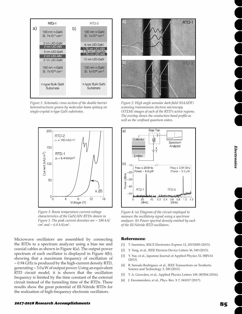
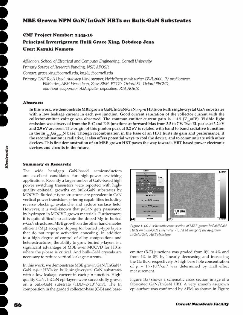
The device structure of the two different RTD designs are displayed in Figure 1. These heterostructures, grown by molecular beam epitaxy (MBE), were fabricated into diodes using contact lithography, metal evaporation and dry etching processes at the Cornell NanoScale Facility (CNF). The main differences between these diodes are the quantum well width and the extension of the spacer regions next to each of the tunneling barriers (See Figure 1). The incorporation of the desired number of monolayers in the barriers and quantum well was confirmed using high angle annular dark-field (HAADF) scanning transmission electron (STEM) microscopy, as shown in Figure 2.
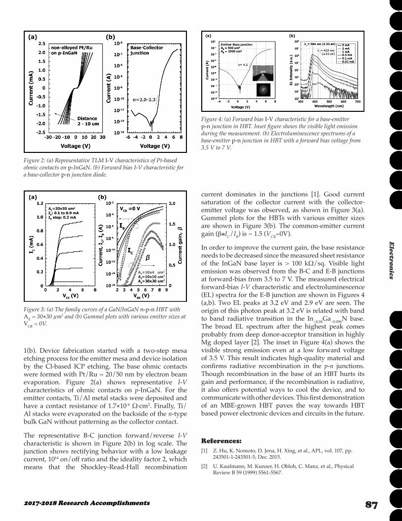
The typical room temperature current-voltage (I-V) characteristics of the devices are displayed in Figure 3. Both RTDs present a characteristic resonant tunneling peak, driving ~ 180 and ~ 6.4 kA/cm2, respectively.
852017-2018 Research Accomplishments
Electron
ics
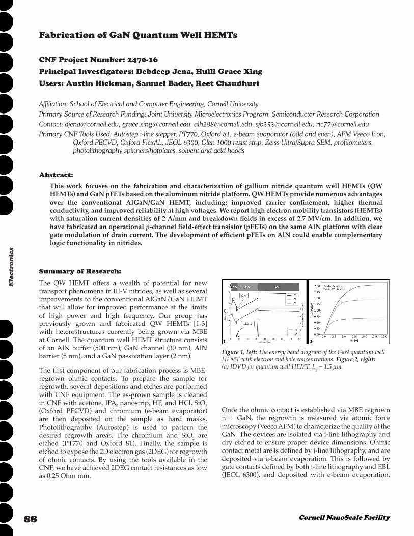
Microwave oscillators are assembled by connecting the RTDs to a spectrum analyzer using a bias tee and coaxial cables as shown in Figure 4(a). The output power spectrum of each oscillator is displayed in Figure 4(b), showing that a maximum frequency of oscillation of ~ 0.94 GHz is produced by the high-current density RTD, generating ~ 3.0 µW of output power. Using an equivalent RTD circuit model, it is shown that the oscillation frequency is limited by the time constant of the external circuit instead of the tunneling time of the RTDs. These results show the great potential of III-Nitride RTDs for the realization of high-frequency electronic oscillators.
Figure 4: (a) Diagram of the circuit employed to measure the oscillatory signal using a spectrum analyzer. (b) Power spectral density emitted by each of the III-Nitride RTD oscillators.
Figure 1: Schematic cross section of the double barrier heterostructures grown by molecular beam epitaxy on single-crystal n-type GaN substrates.
Figure 2: High angle annular dark-field (HAADF) scanning transmission electron microscopy (STEM) images of each of the RTD’s active regions. The overlay shows the conduction band profile as well as the confined quantum states.
Figure 3: Room temperature current-voltage characteristics of the GaN/AlN RTDs shown in Figure 1. The peak current densities are ~ 180 kA/cm2 and ~ 6.4 kA/cm2.
References: [1] T. Suemitsu, IEICE Electronics Express 12, 20152005 (2015).
[2] Y. Tang, et al., IEEE Electron Device Letters 36, 549 (2015).
[3] Y. Yue, et al., Japanese Journal of Applied Physics 52, 08JN14 (2013).
[4] B. Sensale-Rodriguez, et al., IEEE Transactions on Terahertz Science and Technology 3, 200 (2013).
[5] T. A. Growden, et al., Applied Physics Letters 109, 083504 (2016).
[6] J. Encomendero, et al., Phys. Rev. X 7, 041017 (2017).
86 Cornell NanoScale Facility
Ele
ctro
nic
s
MBE Grown NPN GaN/InGaN HBTs on Bulk-GaN Substrates
CNF Project Number: 2443-16
Principal Investigators: Huili Grace Xing, Debdeep Jena
User: Kazuki Nomoto
Affiliation: School of Electrical and Computer Engineering, Cornell UniversityPrimary Source of Research Funding: NSF, AFOSRContact: [email protected], [email protected] CNF Tools Used: Autostep i-line stepper, Heidelberg mask writer DWL2000, P7 profilometer,
FilMetrics, AFM Veeco Icon, Zeiss SEM, PT770, Oxford 81, Oxford PECVD, odd-hour evaporator, AJA sputter deposition, RTA AG610
Abstract:
In this work, we demonstrate MBE grown GaN/InGaN/GaN n-p-n HBTs on bulk single-crystal GaN substrates with a low leakage current in each p-n junction. Good current saturation of the collector current with the collector-emitter voltage was observed. The common-emitter current gain is ~ 1.5 (VCB=0V). Visible light emission was observed from the B-C and E-B junctions at forward-bias from 3.5 to 7 V. Two EL peaks at 3.2 eV and 2.9 eV are seen. The origin of this photon peak at 3.2 eV is related with band to band radiative transition in the In~0.04Ga~0.096N base. Though recombination in the base of an HBT hurts its gain and performance, if the recombination is radiative, it also offers potential ways to cool the device, and to communicate with other devices. This first demonstration of an MBE-grown HBT paves the way towards HBT based power electronic devices and circuits in the future.
Summary of Research:
The wide bandgap GaN-based semiconductors are excellent candidates for high-power switching applications. Recently a large number of GaN-based high power switching transistors were reported with high-quality epitaxial growths on bulk-GaN substrates by MOCVD. Buried p-type structures are prevalent in GaN vertical power transistors, offering capabilities including reverse blocking, avalanche and reduce surface field. However, it is well-known that p-GaN gets passivated by hydrogen in MOCVD grown materials. Furthermore, it is quite difficult to activate the doped-Mg in buried p-GaN structures. MBE growth on the other hand enables efficient (Mg) acceptor doping for buried p-type layers that do not require activation annealing. In addition to a high degree of control of alloy compositions and heterostructures, the ability to grow buried p-layers is a significant advantage of MBE over MOCVD for HBTs, where the p-base is critical. And bulk-GaN crystals are necessary to reduce vertical leakage currents.
In this work, we demonstrate MBE grown GaN/InGaN/GaN n-p-n HBTs on bulk single-crystal GaN substrates with a low leakage current in each p-n junction. High-quality GaN/InGaN epi-layers were successfully grown on a bulk-GaN substrate (TDD~2×10⁷/cm2). The In composition in the graded collector-base (C-B) and base-
Figure 1: (a) A schematic cross section of MBE grown InGaN/GaN HBTs on bulk-GaN substrates. (b) AFM image of the as-grown InGaN/GaN HBT structure.
emitter (B-E) junctions was graded from 0% to 4% and from 4% to 0% by linearly decreasing and increasing the Ga flux, respectively. A high base hole concentration of p ~ 1.7×10¹⁸/cm3 was determined by Hall effect measurement.
Figure 1(a) shows a schematic cross section image of a fabricated GaN/InGaN HBT. A very smooth as-grown epi-surface was confirmed by AFM, as shown in Figure
872017-2018 Research Accomplishments
Electron
ics
1(b). Device fabrication started with a two-step mesa etching process for the emitter mesa and device isolation by the Cl-based ICP etching. The base ohmic contacts were formed with Pt/Ru = 20/50 nm by electron beam evaporation. Figure 2(a) shows representative I-V characteristics of ohmic contacts on p-InGaN. For the emitter contacts, Ti/Al metal stacks were deposited and have a contact resistance of 1.7×10⁻⁴ Ω·cm2. Finally, Ti/Al stacks were evaporated on the backside of the n-type bulk GaN without patterning as the collector contact.
The representative B-C junction forward/reverse I-V characteristic is shown in Figure 2(b) in log scale. The junction shows rectifying behavior with a low leakage current, 1014 on/off ratio and the ideality factor 2, which means that the Shockley-Read-Hall recombination
current dominates in the junctions [1]. Good current saturation of the collector current with the collector-emitter voltage was observed, as shown in Figure 3(a). Gummel plots for the HBTs with various emitter sizes are shown in Figure 3(b). The common-emitter current gain (β≡IC/IB) is ~ 1.5 (VCB=0V).
In order to improve the current gain, the base resistance needs to be decreased since the measured sheet resistance of the InGaN base layer is > 100 kΩ/sq. Visible light emission was observed from the B-C and E-B junctions at forward-bias from 3.5 to 7 V. The measured electrical forward-bias I-V characteristic and electroluminescence (EL) spectra for the E-B junction are shown in Figures 4 (a,b). Two EL peaks at 3.2 eV and 2.9 eV are seen. The origin of this photon peak at 3.2 eV is related with band to band radiative transition in the In~0.04Ga~0.096N base. The broad EL spectrum after the highest peak comes probably from deep donor-acceptor transition in highly Mg doped layer [2]. The inset in Figure 4(a) shows the visible strong emission even at a low forward voltage of 3.5 V. This result indicates high-quality material and confirms radiative recombination in the p-n junctions. Though recombination in the base of an HBT hurts its gain and performance, if the recombination is radiative, it also offers potential ways to cool the device, and to communicate with other devices. This first demonstration of an MBE-grown HBT paves the way towards HBT based power electronic devices and circuits in the future.
References:[1] Z. Hu, K. Nomoto, D. Jena, H. Xing, et al., APL, vol. 107, pp.
243501-1-243501-5, Dec. 2015.
[2] U. Kaufmann, M. Kunzer, H. Obloh, C. Manz, et al., Physical Review B 59 (1999) 5561-5567.
Figure 4: (a) Forward bias I-V characteristic for a base-emitter p-n junction in HBT. Inset figure shows the visible light emission during the measurement. (b) Electroluminescence spectrums of a base-emitter p-n junction in HBT with a forward bias voltage from 3.5 V to 7 V.
Figure 2: (a) Representative TLM I-V characteristics of Pt-based ohmic contacts on p-InGaN. (b) Forward bias I-V characteristic for a base-collector p-n junction diode.
Figure 3: (a) The family curves of a GaN/InGaN n-p-n HBT with AE = 30×30 µm2 and (b) Gummel plots with various emitter sizes at VCB = 0V.
88 Cornell NanoScale Facility
Ele
ctro
nic
s
Fabrication of GaN Quantum Well HEMTs
CNF Project Number: 2470-16
Principal Investigators: Debdeep Jena, Huili Grace Xing
Users: Austin Hickman, Samuel Bader, Reet Chaudhuri
Affiliation: School of Electrical and Computer Engineering, Cornell UniversityPrimary Source of Research Funding: Joint University Microelectronics Program, Semiconductor Research CorporationContact: [email protected], [email protected], [email protected], [email protected], [email protected] CNF Tools Used: Autostep i-line stepper, PT770, Oxford 81, e-beam evaporator (odd and even), AFM Veeco Icon,
Oxford PECVD, Oxford FlexAL, JEOL 6300, Glen 1000 resist strip, Zeiss Ultra/Supra SEM, profilometers, photolithography spinners/hotplates, solvent and acid hoods
Abstract:
This work focuses on the fabrication and characterization of gallium nitride quantum well HEMTs (QW HEMTs) and GaN pFETs based on the aluminum nitride platform. QW HEMTs provide numerous advantages over the conventional AlGaN/GaN HEMT, including: improved carrier confinement, higher thermal conductivity, and improved reliability at high voltages. We report high electron mobility transistors (HEMTs) with saturation current densities of 2 A/mm and breakdown fields in excess of 2.7 MV/cm. In addition, we have fabricated an operational p-channel field-effect transistor (pFETs) on the same AlN platform with clear gate modulation of drain current. The development of efficient pFETs on AlN could enable complementary logic functionality in nitrides.
Summary of Research:
Figure 1, left: The energy band diagram of the GaN quantum well HEMT with electron and hole concentrations. Figure 2, right: (a) IDVD for quantum well HEMT. Lg = 1.5 µm.
The QW HEMT offers a wealth of potential for new transport phenomena in III-V nitrides, as well as several improvements to the conventional AlGaN/GaN HEMT that will allow for improved performance at the limits of high power and high frequency. Our group has previously grown and fabricated QW HEMTs [1-3] with heterostructures currently being grown via MBE at Cornell. The quantum well HEMT structure consists of an AlN buffer (500 nm), GaN channel (30 nm), AlN barrier (5 nm), and a GaN passivation layer (2 nm).
The first component of our fabrication process is MBE-regrown ohmic contacts. To prepare the sample for regrowth, several depositions and etches are performed with CNF equipment. The as-grown sample is cleaned in CNF with acetone, IPA, nanostrip, HF, and HCl. SiO2 (Oxford PECVD) and chromium (e-beam evaporator) are then deposited on the sample as hard masks. Photolithography (Autostep) is used to pattern the desired regrowth areas. The chromium and SiO2 are etched (PT770 and Oxford 81). Finally, the sample is etched to expose the 2D electron gas (2DEG) for regrowth of ohmic contacts. By using the tools available in the CNF, we have achieved 2DEG contact resistances as low as 0.25 Ohm mm.
Once the ohmic contact is established via MBE regrown n++ GaN, the regrowth is measured via atomic force microscopy (Veeco AFM) to characterize the quality of the GaN. The devices are isolated via i-line lithography and dry etched to ensure proper device dimensions. Ohmic contact metal are is defined by i-line lithography, and are deposited via e-beam evaporation. This is followed by gate contacts defined by both i-line lithography and EBL (JEOL 6300), and deposited with e-beam evaporation.
892017-2018 Research Accomplishments
Electron
ics
Finally, the devices are passivated by combinations of SiN, AlN, and Al2O3 via ALD (Oxford FlexAL) and PECVD (Oxford PECVD). The final devices are observed via SEM (Figure 3).
In the past year, the first QW HEMT devices were processed and measured at Cornell. After initial optimization of processing, the QW HEMTs have yielded solid DC performance, with saturation currents over 2 A/mm (Lg = 1.5 µm) and gm = 220 mS/mm, as well as Ebreakdown in excess of 2.7 MV/cm.
In the coming year, the fabrication process will be further optimized for DC and RF performance. With improvements, GaN QW HEMTs can push the limits of high frequency/high power performance of nitride HEMTs, and establish AlN as the optimal platform for the future of nitride electronics.
In addition to high-performance HEMT devices, this platform also provides a natural p-channel transistor
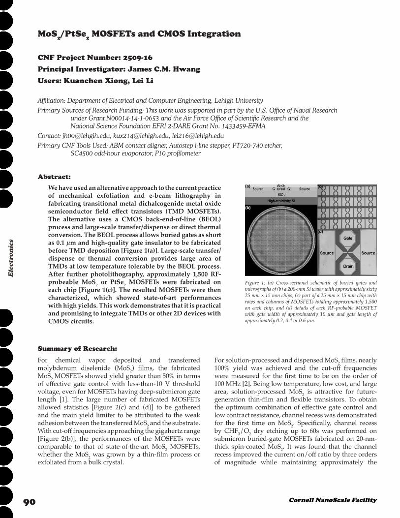
Figure 4: pFET IDVD with clear modulation of drain current. Significant gate leakage limits the device.
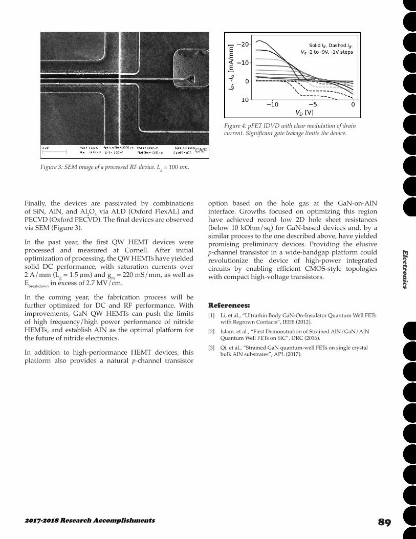
Figure 3: SEM image of a processed RF device. Lg = 100 nm.
option based on the hole gas at the GaN-on-AlN interface. Growths focused on optimizing this region have achieved record low 2D hole sheet resistances (below 10 kOhm/sq) for GaN-based devices and, by a similar process to the one described above, have yielded promising preliminary devices. Providing the elusive p-channel transistor in a wide-bandgap platform could revolutionize the device of high-power integrated circuits by enabling efficient CMOS-style topologies with compact high-voltage transistors.
References:[1] Li, et al., “Ultrathin Body GaN-On-Insulator Quantum Well FETs
with Regrown Contacts”, IEEE (2012).
[2] Islam, et al., “First Demonstration of Strained AlN/GaN/AlN Quantum Well FETs on SiC”, DRC (2016).
[3] Qi, et al., “Strained GaN quantum-well FETs on single crystal bulk AlN substrates”, APL (2017).
90 Cornell NanoScale Facility
Ele
ctro
nic
s
MoS2/PtSe2 MOSFETs and CMOS Integration
CNF Project Number: 2509-16
Principal Investigator: James C.M. Hwang
Users: Kuanchen Xiong, Lei Li
Affiliation: Department of Electrical and Computer Engineering, Lehigh UniversityPrimary Sources of Research Funding: This work was supported in part by the U.S. Office of Naval Research
under Grant N00014-14-1-0653 and the Air Force Office of Scientific Research and the National Science Foundation EFRI 2-DARE Grant No. 1433459-EFMA
Contact: [email protected], [email protected], [email protected] CNF Tools Used: ABM contact aligner, Autostep i-line stepper, PT720-740 etcher,
SC4500 odd-hour evaporator, P10 profilometer
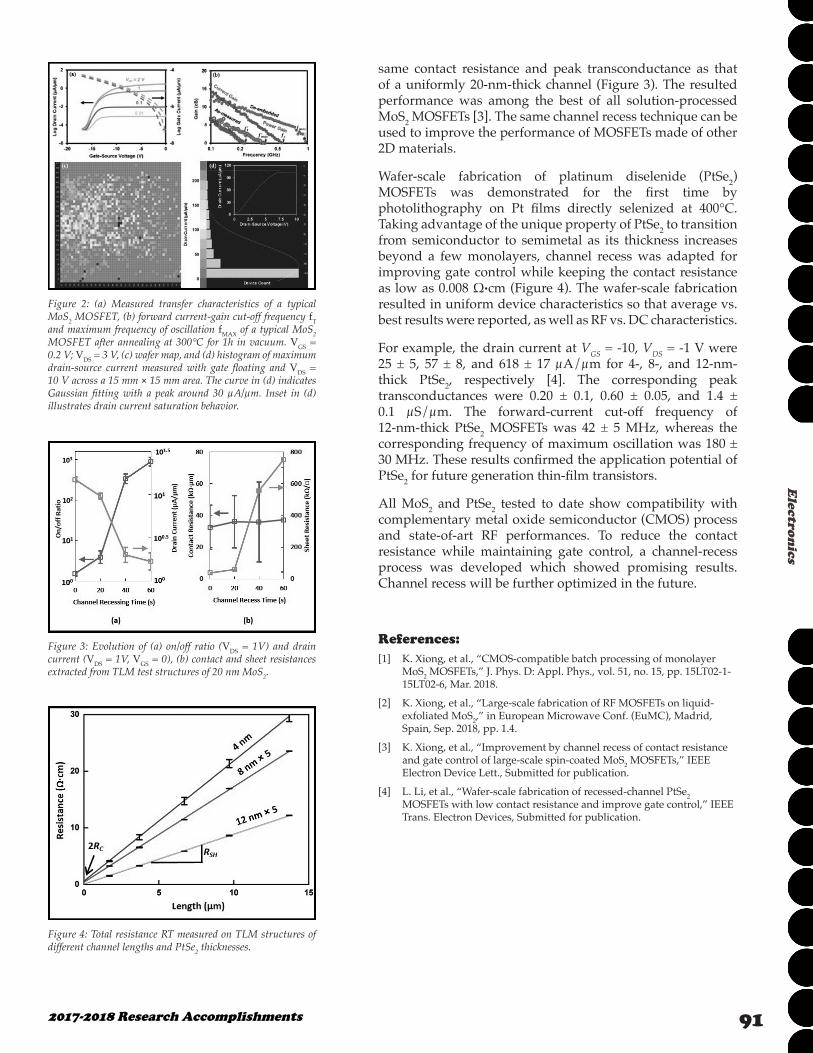
Abstract:
Figure 1: (a) Cross-sectional schematic of buried gates and micrographs of (b) a 200-mm Si wafer with approximately sixty 25 mm × 15 mm chips, (c) part of a 25 mm × 15 mm chip with rows and columns of MOSFETs totaling approximately 1,500 on each chip, and (d) details of each RF-probable MOSFET with gate width of approximately 10 µm and gate length of approximately 0.2, 0.4 or 0.6 µm.
We have used an alternative approach to the current practice of mechanical exfoliation and e-beam lithography in fabricating transitional metal dichalcogenide metal oxide semiconductor field effect transistors (TMD MOSFETs). The alternative uses a CMOS back-end-of-line (BEOL) process and large-scale transfer/dispense or direct thermal conversion. The BEOL process allows buried gates as short as 0.1 µm and high-quality gate insulator to be fabricated before TMD deposition [Figure 1(a)]. Large-scale transfer/dispense or thermal conversion provides large area of TMDs at low temperature tolerable by the BEOL process. After further photolithography, approximately 1,500 RF-probeable MoS2 or PtSe2 MOSFETs were fabricated on each chip [Figure 1(c)]. The resulted MOSFETs were then characterized, which showed state-of-art performances with high yields. This work demonstrates that it is practical and promising to integrate TMDs or other 2D devices with CMOS circuits.
Summary of Research:
For chemical vapor deposited and transferred molybdenum diselenide (MoS2) films, the fabricated MoS2 MOSFETs showed yield greater than 50% in terms of effective gate control with less-than-10 V threshold voltage, even for MOSFETs having deep-submicron gate length [1]. The large number of fabricated MOSFETs allowed statistics [Figure 2(c) and (d)] to be gathered and the main yield limiter to be attributed to the weak adhesion between the transferred MoS2 and the substrate. With cut-off frequencies approaching the gigahertz range [Figure 2(b)], the performances of the MOSFETs were comparable to that of state-of-the-art MoS2 MOSFETs, whether the MoS2 was grown by a thin-film process or exfoliated from a bulk crystal.
For solution-processed and dispensed MoS2 films, nearly 100% yield was achieved and the cut-off frequencies were measured for the first time to be on the order of 100 MHz [2]. Being low temperature, low cost, and large area, solution-processed MoS2 is attractive for future-generation thin-film and flexible transistors. To obtain the optimum combination of effective gate control and low contract resistance, channel recess was demonstrated for the first time on MoS2. Specifically, channel recess by CHF3/O2 dry etching up to 60s was performed on submicron buried-gate MOSFETs fabricated on 20-nm-thick spin-coated MoS2. It was found that the channel recess improved the current on/off ratio by three orders of magnitude while maintaining approximately the
912017-2018 Research Accomplishments
Electron
ics
same contact resistance and peak transconductance as that of a uniformly 20-nm-thick channel (Figure 3). The resulted performance was among the best of all solution-processed MoS2 MOSFETs [3]. The same channel recess technique can be used to improve the performance of MOSFETs made of other 2D materials.
Wafer-scale fabrication of platinum diselenide (PtSe2) MOSFETs was demonstrated for the first time by photolithography on Pt films directly selenized at 400°C. Taking advantage of the unique property of PtSe2 to transition from semiconductor to semimetal as its thickness increases beyond a few monolayers, channel recess was adapted for improving gate control while keeping the contact resistance as low as 0.008 Ω∙cm (Figure 4). The wafer-scale fabrication resulted in uniform device characteristics so that average vs. best results were reported, as well as RF vs. DC characteristics.
For example, the drain current at VGS = -10, VDS = -1 V were 25 ± 5, 57 ± 8, and 618 ± 17 µA/µm for 4-, 8-, and 12-nm-thick PtSe2, respectively [4]. The corresponding peak transconductances were 0.20 ± 0.1, 0.60 ± 0.05, and 1.4 ± 0.1 µS/µm. The forward-current cut-off frequency of 12-nm-thick PtSe2 MOSFETs was 42 ± 5 MHz, whereas the corresponding frequency of maximum oscillation was 180 ± 30 MHz. These results confirmed the application potential of PtSe2 for future generation thin-film transistors.
All MoS2 and PtSe2 tested to date show compatibility with complementary metal oxide semiconductor (CMOS) process and state-of-art RF performances. To reduce the contact resistance while maintaining gate control, a channel-recess process was developed which showed promising results. Channel recess will be further optimized in the future.
References:[1] K. Xiong, et al., “CMOS-compatible batch processing of monolayer
MoS2 MOSFETs,” J. Phys. D: Appl. Phys., vol. 51, no. 15, pp. 15LT02-1-15LT02-6, Mar. 2018.
[2] K. Xiong, et al., “Large-scale fabrication of RF MOSFETs on liquid-exfoliated MoS2,” in European Microwave Conf. (EuMC), Madrid, Spain, Sep. 2018, pp. 1.4.
[3] K. Xiong, et al., “Improvement by channel recess of contact resistance and gate control of large-scale spin-coated MoS2 MOSFETs,” IEEE Electron Device Lett., Submitted for publication.
[4] L. Li, et al., “Wafer-scale fabrication of recessed-channel PtSe2 MOSFETs with low contact resistance and improve gate control,” IEEE Trans. Electron Devices, Submitted for publication.
Figure 4: Total resistance RT measured on TLM structures of different channel lengths and PtSe2 thicknesses.
Figure 2: (a) Measured transfer characteristics of a typical MoS2 MOSFET, (b) forward current-gain cut-off frequency fT and maximum frequency of oscillation fMAX of a typical MoS2 MOSFET after annealing at 300°C for 1h in vacuum. VGS = 0.2 V; VDS = 3 V, (c) wafer map, and (d) histogram of maximum drain-source current measured with gate floating and VDS = 10 V across a 15 mm × 15 mm area. The curve in (d) indicates Gaussian fitting with a peak around 30 µA/µm. Inset in (d) illustrates drain current saturation behavior.
Figure 3: Evolution of (a) on/off ratio (VDS = 1V) and drain current (VDS = 1V, VGS = 0), (b) contact and sheet resistances extracted from TLM test structures of 20 nm MoS2.
92 Cornell NanoScale Facility
Ele
ctro
nic
s
Fabrication of FETs Based on La-BaSnO3 Perovskite Oxide
CNF Project Number: 2543-17
Principal Investigator: Darrell Schlom
User: Jisung Park
Affiliation: Department of Material Science and Engineering, Cornell University, Ithaca, NY 14853, USAPrimary Source of Research Funding: Air Force Office of Scientific Research – DODContact: [email protected], [email protected] CNF Tools Used: PVD75 sputter deposition, AJA ion mill, Oxford ALD FlexAL
Abstract:
A field effect transistor based on La-BaSnO3 (BLSO) has been made. The BLSO is a perovskite oxide material with high mobility and oxygen stability. The BLSO film was grown by molecular beam epitaxy. It has been etched with the AJA ion mill to make a channel layer, and ITO is deposited on the channel layer as the source and drain contact layer by PVD75 sputter deposition. ALD-grown HfO2 film was deposited on it as a dielectric oxide by Oxford ALD FlexAL. ITO is deposited again by the same tool as a gate electrode. The schematic is shown in Figure 1. The device shows good characteristic curve in terms of Ids-Vds and Ids-Vgs. The on-off ratio is over 6 × 10⁶ and mobility is over 20 cm2/V∙s. The characteristic curve of the device is shown in Figure 2 and Figure 3.
Summary of Research:
Figure 2, left: Output characteristic curve of the device. Figure 3, right: Transfer characteristic of the device.
Field effect transistor based on La-BaSnO3 (BLSO) has been fabricated and nice characteristic curves with high on-off ratio over 6 × 10⁶ and mobility over 20 cm2/V∙s has been shown.
References:[1] H. J. Kim, U. Kim, H. M. Kim, T. H. Kim, H. S. Mun, B.-G. Jeon,
K. T. Hong, W.-J. Lee, C. Ju, K. H. Kim, and K. Char, Appl. Phys. Express 5, 061102 (2012).
[2] C. Park, U. Kim, C. J. Ju, J. S. Park, Y. M. Kim, and K. Char, Appl. Phys. Lett. 105, 203503 (2014).
[3] Y. M. Kim, C. Park, U. Kim, C. Ju, and K. Char, Appl. Phys. Express 9, 011201 (2016).
[4] U. Kim, C. Park, T. Ha, Y. M. Kim, N. Kim, C. Ju, J. Park, J. Yu, J. H. Kim, and K. Char, APL Mater. 3, 036101 (2015).
Figure 1: Schematic of the filed effect transistor based on La-BaSnO3.

932017-2018 Research Accomplishments
Electron
ics
94 Cornell NanoScale Facility
Ele
ctro
nic
s
Micro-Scale Opto-Electrically Transduced Electrodes (MOTEs)
CNF Project Number: 2578-17
Principal Investigator: Prof. Alyosha C. Molnar
Users: Sunwoo Lee, Alejandro Cortese
Affiliation: Electrical and Computer Engineering, Cornell UniversityPrimary Source of Research Funding: National Institute of HealthContact: [email protected], [email protected]: https://molnargroup.ece.cornell.edu/Primary CNF Tools Used: ABM contact aligner, AJA sputter deposition, Westbond 7400A ultrasonic wire bonder
Abstract:
Recording neural activity in live animals in vivo poses several challenges. Electrical techniques often require electrodes to be tethered to the outside world directly via a wire, or indirectly via an RF coil [1], which is much larger than the electrodes themselves. Tethered implants result in residual motion between neurons and electrodes as the brain moves and limits our ability to measure from peripheral nerves in moving animals, especially in smaller organisms such as zebra fish or fruit flies. On the other hand, optical techniques, which are becoming increasingly powerful, are nonetheless often limited to subsets of neurons in any given organism, impeded by scattering of the excitation light and emitted fluorescence, and limited to low temporal resolution [2]. In our work, an untethered electrode unit capable of signal amplification and modulation is powered by, and communicates through a microscale optical interface, combining many benefits of optical techniques with high temporal-resolution recording of electrical signals [3]. To combine conventional complementary metal-oxide semiconductor (CMOS) for electronics and aluminum gallium arsenide (AlGaAs) light emitting didoes (LEDs) for optical functionalities, CNF has provided pivotal supports in fabricating the said hetero-integration.
Summary of Research:
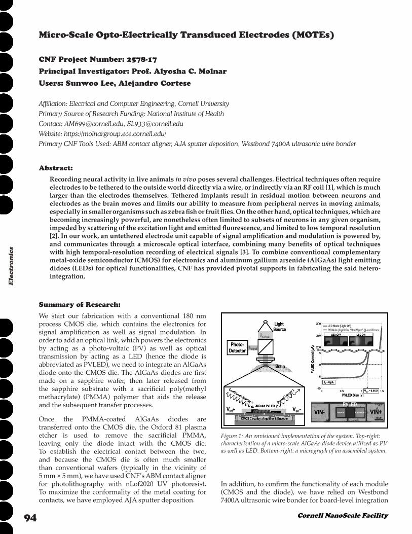
Figure 1: An envisioned implementation of the system. Top-right: characterization of a micro-scale AlGaAs diode device utilized as PV as well as LED. Bottom-right: a micrograph of an assembled system.
We start our fabrication with a conventional 180 nm process CMOS die, which contains the electronics for signal amplification as well as signal modulation. In order to add an optical link, which powers the electronics by acting as a photo-voltaic (PV) as well as optical transmission by acting as a LED (hence the diode is abbreviated as PVLED), we need to integrate an AlGaAs diode onto the CMOS die. The AlGaAs diodes are first made on a sapphire wafer, then later released from the sapphire substrate with a sacrificial poly(methyl methacrylate) (PMMA) polymer that aids the release and the subsequent transfer processes.
Once the PMMA-coated AlGaAs diodes are transferred onto the CMOS die, the Oxford 81 plasma etcher is used to remove the sacrificial PMMA, leaving only the diode intact with the CMOS die. To establish the electrical contact between the two, and because the CMOS die is often much smaller than conventional wafers (typically in the vicinity of 5 mm × 5 mm), we have used CNF’s ABM contact aligner for photolithography with nLof2020 UV photoresist. To maximize the conformality of the metal coating for contacts, we have employed AJA sputter deposition.
In addition, to confirm the functionality of each module (CMOS and the diode), we have relied on Westbond 7400A ultrasonic wire bonder for board-level integration
952017-2018 Research Accomplishments
Electron
ics
efforts. We have also employed parylene deposition and the Oxford ALD FlexAL for passivation of the assembled heterostructure. Finally, ZEISS Ultra and Supra scanning electron microscopes (SEMs) are used to inspect the fabricated MOTE that is shown in Figure 1.
The assembled MOTE implements pulse position modulation (PPM) for signal encoding for its high information-per-photon efficiency and the diode, the PVLED delivers sharp (<100ns) current pulses, spacings of which are proportional to the measured electric field of neuronal signals across the measurement electrodes (two outer-most electrodes shown on the bottom right of Figure 1). Furthermore, it should be noted that the PVLEDs with different wavelengths can provide further disambiguation via wavelength multiplexing, providing a path towards many-MOTE probing of neural signals.
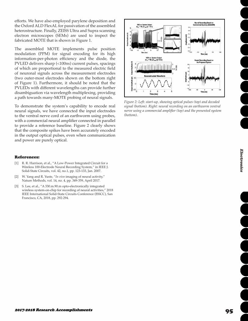
To demonstrate the system’s capability to encode real neural signals, we have connected the input electrodes to the ventral nerve cord of an earthworm using probes, with a commercial neural amplifier connected in parallel to provide a reference baseline. Figure 2 clearly shows that the composite spikes have been accurately encoded in the output optical pulses, even when communication and power are purely optical.
References:[1] R. R. Harrison, et al., “A Low-Power Integrated Circuit for a
Wireless 100-Electrode Neural Recording System,” in IEEE J. Solid-State Circuits, vol. 42, no.1, pp. 123-133, Jan. 2007.
[2] W. Yang and R. Yuste, “In vivo imaging of neural activity,” Nature Methods, vol. 14, no. 4, pp. 349-359, April 2017.
[3] S. Lee, et al., “A 330.m.90.m opto-electronically integrated wireless system-on-chip for recording of neural activities,” 2018 IEEE International Solid-State Circuits Conference (ISSCC), San Francisco, CA, 2018, pp. 292-294.
Figure 2: Left: start-up, showing optical pulses (top) and decoded signal (bottom). Right: neural recording on an earthworm ventral nerve using a commercial amplifier (top) and the presented system (bottom).