Embed Size (px)
Citation preview
This content has been downloaded from IOPscience. Please scroll down to see the full text.
Download details:
IP Address: 139.179.66.241
This content was downloaded on 17/10/2016 at 08:29
Please note that terms and conditions apply.
You may also be interested in:
Hybrid chemical etching of femtosecond laser irradiated structures for engineered microfluidic
devices
S LoTurco, R Osellame, R Ramponi et al.
Crack-free direct-writing on glass using a low-power UV laser
Ji-Yen Cheng, Meng-Hua Yen, Cheng-Wey Wei et al.
Rapid cell-patterning and microfluidic chip fabrication on glass
Meng-Hua Yen, Ji-Yen Cheng, Cheng-Wey Wei et al.
Characterization of deep wet etching of fused silica glass for single cell and optical sensor
deposition
Haixin Zhu, Mark Holl, Tathagata Ray et al.
Fabrication of microfluidic systems onsoda-lime glass
Che-Hsin Lin, Gwo-Bin Lee, Yen-Heng Lin et al.
Laser stenciling: a low-cost high-resolution CO2 laser micromachining method
Whitney Longsine-Parker and Arum Han
CO2 laser polishing of microfluidic channels fabricated by femtosecond laser assisted carving
View the table of contents for this issue, or go to the journal homepage for more
2016 J. Micromech. Microeng. 26 115011
(http://iopscience.iop.org/0960-1317/26/11/115011)
Home Search Collections Journals About Contact us My IOPscience
1 © 2016 IOP Publishing Ltd Printed in the UK
1. Introduction
In the last two decades there has been increased demand for microfluidic lab-on-a-chip platforms towards rapid bio-anal-ysis, drug development, and delivery while using a smaller sample quantity. Currently, common materials for microfluidic devices include polymers, silicon and glass. While polymers offer cost effective and relatively easier fabrication through soft lithography, injection molding, and hot embossing, they
lack the stability for long-term or multi-use applications due to their absorptive nature [1]. Silicon shows better chemical and mechanical stability, and is a good candidate for CMOS integration. However, it suffers from optical absorption in the visible wavelength range, thus is not preferred for opto-fluidic applications [2]. Glass surfaces are chemically inert, mechanically stable, and optically transparent to a wide spec-trum of light. On the other hand, the fabrication of glass-based microfluidic systems with well-known cleanroom fabrication
Journal of Micromechanics and Microengineering
CO2 laser polishing of microfluidic channels fabricated by femtosecond laser assisted carving
Murat Serhatlioglu1,2, Bülend Ortaç1,2, Caglar Elbuken1,2, Necmi Biyikli1,2 and Mehmet E Solmaz3
1 UNAM—National Nanotechnology Research Center, Bilkent University, 06800, Ankara, Turkey2 Institute of Materials Science and Nanotechnology, Bilkent University, 06800, Ankara, Turkey3 Department of Electrical and Electronics Engineering, Izmir Katip Celebi University, 35620, Izmir, Turkey
E-mail: [email protected]
Received 10 May 2016, revised 6 July 2016Accepted for publication 20 July 2016Published 5 October 2016
AbstractIn this study, we investigate the effects of CO2 laser polishing on microscopic structures fabricated by femtosecond laser assisted carving (FLAC). FLAC is the peripheral laser irradiation of 2.5D structures suitable for low repetition rate lasers and is first used to define the microwell structures in fused silica followed by chemical etching. Subsequently, the bottom surface of patterned microwells is irradiated with a pulsed CO2 laser. The surfaces were characterized using an atomic force microscope (AFM) and scanning electron microscope (SEM) in terms of roughness and high quality optical imaging before and after the CO2 laser treatment. The AFM measurements show that the surface roughness improves more than threefold after CO2 laser polishing, which promises good channel quality for applications that require optical imaging. In order to demonstrate the ability of this method to produce low surface roughness systems, we have fabricated a microfluidic channel. The channel is filled with polystyrene bead-laden fluid and imaged with transmission mode microscopy. The high quality optical images prove CO2 laser processing as a practical method to reduce the surface roughness of microfluidic channels fabricated by femtosecond laser irradiation. We further compared the traditional and laser-based glass micromachining approaches, which includes FLAC followed by the CO2 polishing technique.
Keywords: femtosecond laser machining, CO2 laser, microfluidics, polishing, surface characterization
(Some figures may appear in colour only in the online journal)
M Serhatlioglu et al
Printed in the UK
115011
JMMIEZ
© 2016 IOP Publishing Ltd
2016
26
J. Micromech. Microeng.
JMM
0960-1317
10.1088/0960-1317/26/11/115011
Paper
11
Journal of Micromechanics and Microengineering
IOP
0960-1317/16/115011+9$33.00
doi:10.1088/0960-1317/26/11/115011J. Micromech. Microeng. 26 (2016) 115011 (9pp)
M Serhatlioglu et al
2
techniques (photolithography, wet etching, dry etching etc) is costly and requires time consuming processing steps [3–5].
Femtosecond laser micromachining of high band-gap transparent glass structures using ultrashort laser pulses is a well-known fabrication technique which relies on nonlinear multiphoton absorption phenomenon [6]. Different irradiation schemes and high power laser machining techniques are given in the literature for the femtosecond laser micromachining process [7–10]. They mainly require irradiation of the sample with tightly focused femtosecond laser beam followed by etching in hydrofluoric (HF) acid. This technique is also called femtosecond laser irradiation followed by chemical etching (FLICE) [11]. There is also hybrid version of the FLICE tech-nique which requires using HF acid together with potassium hydroxide (KOH), as H-FLICE, which is mainly useful for preserving structural dimensions and avoids the conical shape change in longer etching durations [12].
FLICE enables the fabrication of complex structures in fused silica for microfluidic channels [1, 13, 14], and mon-olithic integrated devices [15–17]. For rectangular-shaped surfaces and buried structures in glass, FLICE initially scans the full 2.5D volume of the pattern layer by layer. The layers are composed of lines with constant separation. Every layer is separated by a predetermined height [8]. Although traditional FLICE can be used to fabricate complicated geometries, it is a rather slow method due to the irradiation of the entire volume and tedious etching step. Bragheri et al tried to solve this problem by scanning the lateral surface of the buried channel [18]. This technique required additional scanning of smaller geometries inside the channel and depends on a slow and difficult etching process, where initial scan geometry is not preserved.
When FLICE or H-FLICE is combined with high repeti-tion rate lasers (~1 MHz—short time interval between each pulse about—1 µs cause cumulative heat transfer which allows control the size of machined area), it provides higher scanning speed which is critical for achieving complex pat-terns and longer channels in a reasonable amount of time due to a combination of pulse number and energy per area require-ment [11, 19, 20]. Yet the scanning speed for low repetition rate lasers (~1 kHz—time interval between each pulse, long enough to carry away the heat from the focus point before the other pulse arrives) is in the order of tens of micrometers per second in order to keep tracking enough energy pulse train on substrate, which results in extremely long processing times for long microfluidic channels and complex 2.5D structures to achieve high structured surface quality. Also, solid state femtosecond lasers are sensitive to changes in laboratory con-ditions such as room temperature, humidity, and thermal and mechanical perturbations which may affect the performance of laser over time.
Femtosecond laser processed glass systems are used for many biochemical analysis systems [21]. Nevertheless, the optical quality of the etched surfaces is not suitable for imaging purposes due to micro-pits, which are byproducts of laser pro-cessing. After laser irradiation and HF etching, it is difficult to achieve smooth and flat surfaces similar to non-treated glass. Osellame et al demonstrated a monolithic glass chip for optical
trapping and stretching of single cells [15]. Even though the cells are visible under microscope images during stretching, the surface roughness of the channels degrades axial resolu-tion. Similar concerns arise for an imaging flow cytometry system with femtosecond laser-micromachined glass micro-fluidic channels [1]. The background image is subtracted from the image with cells for better threshold differentiation of the cell boundaries for image processing application.
CO2 laser processing is a powerful technique for local heat treatment and material modification particularly the polishing of rough surfaces on glass-based materials [22]. The high absorption coefficient of CO2 laser radiation in silica is caused by elastic vibration of the oxygen atom in between two silicon atoms (Si–O–Si) which results in local heating [23]. The CO2 laser energy is mainly absorbed in a thin surface layer and does not affect the rest of the material [24]. There are recent studies that use a CO2 laser to reshape the 3D patterns fabri-cated with femtosecond laser micromachining. For instance, Sohn et al conically micro-machined a fiber tip with femto-second laser ablation and polished the fiber tip with CO2 laser to demonstrate a bidirectional firing optical fiber [25]. Kim et al (2014) showed a fused silica-based mold for a microlen-ticular lens array using femtosecond laser ablation, followed with CO2 laser polishing [26]. Bellouard et al showed the con-trollable CO2 laser application to transform femtosecond laser micromachined cubic box to a spherical shape [27].
Here we report femtosecond laser assisted carving (FLAC) to drastically reduce the scanning time mainly aimed for low repetition rate femtosecond lasers. We investigate the sur-face roughness of FLAC fabricated surfaces using optical microscope, scanning electron microscope (SEM) and atomic force microscope (AFM) images and we introduce the CO2 laser treatment process for the polishing of such surfaces to reduce roughness. We fabricated microfluidic channels to demonstrate the improvement in optical imaging using poly-styrene microspheres. We finally compare FLAC and FLICE with traditional glass micromachining techniques in terms of machining time, precision, roughness, aspect ratio, min-imum feature size, cost, reproducibility, etch rate and parallel processing.
2. Experimental methods
The experimental method for the FLAC fabrication technique is divided into four sub-sections.
2.1. Femtosecond laser assisted carving (FLAC)
A Ti:Sapphire femtosecond laser amplifier, operating at 800 nm wavelength, sub-500 fs pulse duration, 1 kHz rep-etition rate and 3 W average power output femtosecond laser is coupled to a custom-made bright field microscopy setup. Microscope setup is combined with high precision linear XYZ translation stage (M406 precision linear stage for X–Y and M501 precision Z-stage from Physik Instrumente) in order to automatically operate the system with DC motor controller (PI-C884). The output power of femtosecond laser is tuned with
J. Micromech. Microeng. 26 (2016) 115011
M Serhatlioglu et al
3
half wave plate and polarizer. A 50× magnification, 11 mm extra-long working distance, 0.60 numerical aperture, 4 mm focal length, 0.91 µm depth of focus, infinity corrected objec-tive lens is used to tightly focus the laser beam onto the fused silica sample. The 2.5D pattern is designed in AUTOCAD and is transferred to a XYZ stage controller via a command set. 1 mm thick, 25 × 75 mm2 JGS1 grade high purity fused silica slides are used as samples. 1 mW average power and 60 µm s−1 translation speed are used for the fabrication of the microwells and microfluidic channels. Microfluidic channel inlets and outlets are drilled with 6 mW average power and 240 µm s−1 helical translation speed to precisely obtain the 1.46 mm diameter for fluidic connections that results in a tight connection with the 1.5 mm diameter tygon tubing for fluidic access.
2.2. Chemical etching
After femtosecond laser radiation of the 2.5D pattern, the sample is dipped into an ultrasonic bath (Branson-2510) with aqueous solution of 10% (for microwells) and 20% (for microfluidic channels on test chip) HF acid in a Teflon beaker. In order to prevent HF splashing out of the beaker, it is carefully capped and enclosed during ultra-sonication of samples.
2.3. CO2 laser polishing
A CO2 laser (Epilog Zing 30 W) is used in raster scan mode for polishing the bottom surfaces of etched samples. The laser operates at 10.6 µm wavelength with 5 kHz frequency and the maximum output power is 30 W. We optimized CO2 laser pol-ishing parameters in order to obtain the best polishing results in terms of surface roughness: 1000 DPI with ~100 µm beam diameter, ~1.8 W laser power, and 6 mm s−1 speed. The CO2 laser scanning step size of ~25 µm as per the manufacturers information was verified by doing an experiment at 1000 DPI with various power levels.
2.4. Adhesive free fused silica glass bonding
Thermal bonding was used to bond two fused silica samples without using any adhesive layer inbetween. First, the glass samples were thoroughly cleaned with Piranha solution then aligned and strongly pressed together using strong NdFeB magnets while the surfaces were still wet. Fabrication of the microfluidic chip was completed by placing the chip into a high temperature furnace for 7 h at 650 °C. The two surfaces were physically bonded to each other with van der Waals forces after they were dried [22].
3. Results and discussion
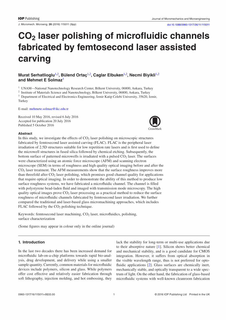
Figure 1 reports an illustration of the FLAC technique. Instead of radiating full sample volume, line by line and layer by layer as in FLICE, it only requires irradiation of the frame of the volume.
As shown in figure 1(a) the microwell sidewalls are scanned with a constant �z separation distance. The bottom layer is raster scanned with a constant separation in the �x direction. A total of five surfaces are scanned for a rectan-gular-shaped microwell pattern on the surface on the sample. The bottom layer forms a buried channel and the sidewalls act as the etching path for the HF acid. After laser exposure, the sample is immersed in HF solution, where HF attacks from the sidewalls of the design and reaches to the bottom surface to completely etch out the irradiated bottom layer. Finally, the 2.5D structure is released from the sample and the carved channel remains with the desired pattern as illustrated in figure 1(b).
It is critical to compare the speed of FLAC and traditional FLICE methods for structures patterned on the surface. For a microfluidic channel with a 200 × 200 µm2 cross section and 1 mm length which is irradiated with 5 µm layer and 3 µm line separation, FLAC is ~16 times faster than FLICE, since FLAC only traces the outer surfaces of the 2.5D pattern.
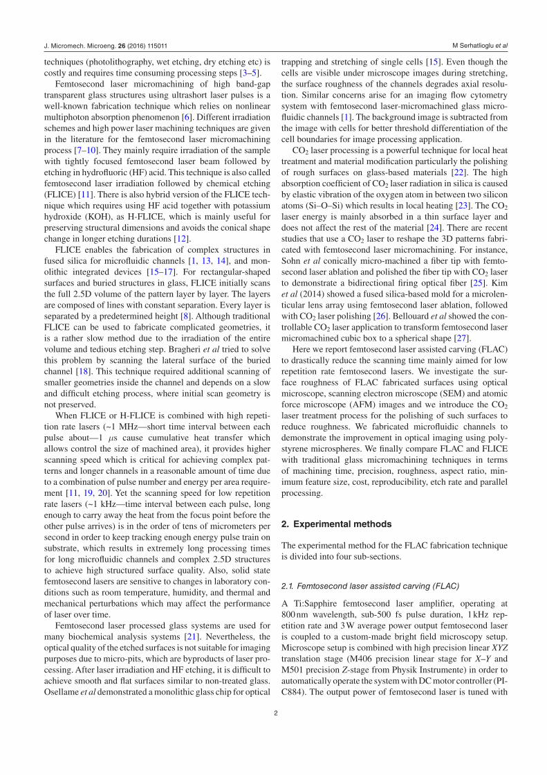
The progress of HF etching on a 500 × 500 × 40 µm3 microwell structure fabricated with FLAC is given in figure 2. After the femtosecond laser fully scans the 2.5D pattern, the sample is dipped into the ultrasonic bath with 10% HF acid in an aqueous solution. The HF acid penetrates and etches selectively through the laser exposed area. The etching time depends on the direction of scanning with respect to the polarization of light, size of the pattern and exposure method. For the microwell reported here, the polarization of laser light is perpendicular for the horizontal sidewalls and parallel in the vertical sidewalls, with respect to the
Figure 1. (a) Illustrative figure of irradiation of the outer surfaces of a microwell with FLAC process; (b) released 2.5D material from fused silica substrate after chemical etching.
J. Micromech. Microeng. 26 (2016) 115011
M Serhatlioglu et al
4
writing direction. This leads to the vertical sidewalls being etched slower than the horizontal sidewalls, as also seen in figures 2(b) and (c), which can be corrected by adjusting the polarization during laser scanning. The HF starts to penetrate through the sidewalls in 5 min and etches beneath the full volume through all of the irradiated bottom surface in about 40 min. The time taken for the HF to reach the bottom layer can be controlled by changing the depth of the pattern and adjusting the laser parameters (laser power and polarization). Since HF is in contact with the sidewalls for a longer time before reaching the bottom surface, it results in a slightly expanded microwell width. The same irregularity happens at the bottom surface where the etching solution first attacks from the edges and finally reaches the center of the bottom surface; a dome shape with small curvature is formed. These deteriorations can be corrected by pre-processing the 2.5D scanning pattern prior to femtosecond laser irradiation or using KOH etchant which has very low etching rate for non-treated fused silica [12].
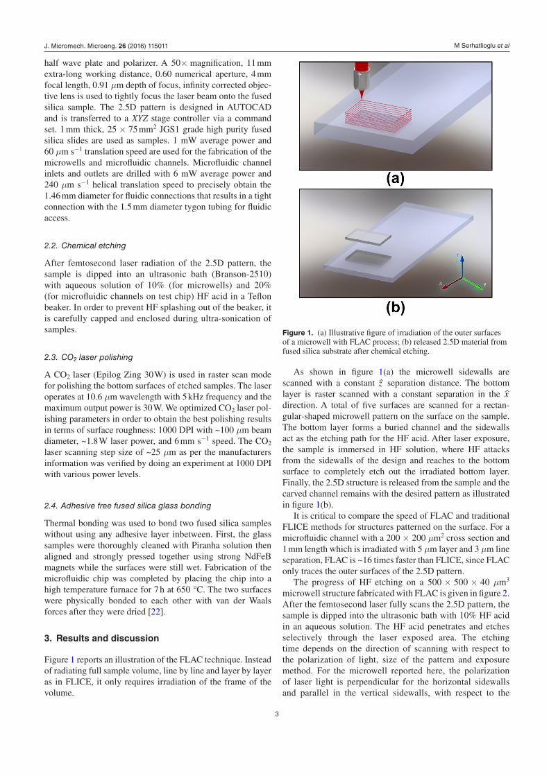
To show that FLAC can be applied to larger patterns and to eliminate the dome shape on the bottom surface, a partitioning approach is applied where larger patterns are divided into smaller regions. As shown in figure 3, a micro-fluidic T-junction design was divided into smaller rectangles during the irradiation process. Here, again 40 µm deep, but bigger 1 × 1 mm2 square reservoirs were divided into five 1 × 0.2 mm2 rectangles to observe the FLAC process. Hence, microfluidic wells in the order of millimeters can be rapidly processed using FLAC with a much improved etch rate using the partitioning approach.
In order to see the effect of CO2 laser polishing, we pre-pared 40 µm deep and 400 × 400 µm2 square microwell structures on fused silica with FLAC, and raster scanned with
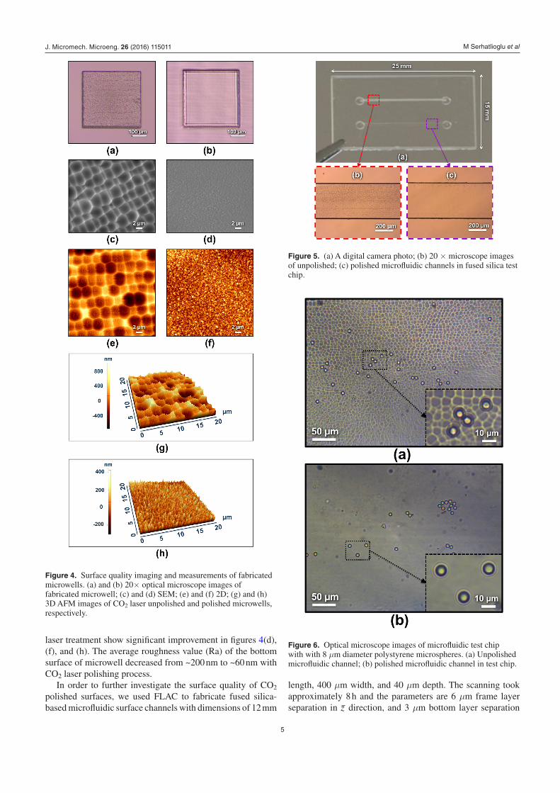
the CO2 laser. The examination results for polished and unpol-ished samples are given in figure 4.
The optical transmission mode inverted microscope images (Zeiss Axio Vert.A1) shown in figures 4(a) and (b) clearly illustrate the effect of CO2 laser polishing. The roughness on the bottom surface of the non-polished microwell causes less transmission compared to its surroundings. On the other hand, the transmission quality of the surface is equal in all sides of the microwell after CO2 laser polishing. It is worth noting that the area of CO2 raster scan is larger than the microwell pattern and this results in periodic surface fluctuations at the outside of the microwell depending on the raster resolution shown in figure 4(b).
For detailed comparison of polished and unpolished sur-faces, we used Nova NanoSEM with helix detector in low vacuum mode in order to analyze the fused silica samples without a thin film metal coating. PSIA XE-100 AFM was used to investigate the topographic data of surface roughness from a 20 × 20 µm2 area of CO2 laser treated and untreated samples. SEM and AFM images show organized micro-pits on the surface as a result of micro-explosions due to very high energy laser beam focusing inside the transparent material during the femtosecond laser irradiation in figures 4(c), (e), and (h). The FLAC microwells that are polished with CO2
Figure 2. Time-lapse 20× optical micrographs of a 500 × 500 × 40 µm3 microwell fabricated with FLAC during HF chemical etching. Images after (a) 0 min, (b) 5 min, (c) 12 min, (d) 25 min, (e) 30 min, and (f) 40 min. The etchant starts attacking the bottom surface after only 5 min for this geometry.
Figure 3. Time-lapse 10× optical images of microfluidic T-junction device fabricated with FLAC during HF chemical etching. Images after (a) 0 min, (b) 10 min, (c) 15 min, (d) 20 min, (e) 25 min, and (f) 30 min. The etchant penetrated through the sidewalls of entire design and defined small rectangular divisions as well.
J. Micromech. Microeng. 26 (2016) 115011
M Serhatlioglu et al
5
laser treatment show significant improvement in figures 4(d), (f), and (h). The average roughness value (Ra) of the bottom surface of microwell decreased from ~200 nm to ~60 nm with CO2 laser polishing process.
In order to further investigate the surface quality of CO2 polished surfaces, we used FLAC to fabricate fused silica-based microfluidic surface channels with dimensions of 12 mm
length, 400 µm width, and 40 µm depth. The scanning took approximately 8 h and the parameters are 6 µm frame layer separation in z direction, and 3 µm bottom layer separation
Figure 4. Surface quality imaging and measurements of fabricated microwells. (a) and (b) 20× optical microscope images of fabricated microwell; (c) and (d) SEM; (e) and (f) 2D; (g) and (h) 3D AFM images of CO2 laser unpolished and polished microwells, respectively.
Figure 5. (a) A digital camera photo; (b) 20 × microscope images of unpolished; (c) polished microfluidic channels in fused silica test chip.
Figure 6. Optical microscope images of microfluidic test chip with with 8 µm diameter polystyrene microspheres. (a) Unpolished microfluidic channel; (b) polished microfluidic channel in test chip.
J. Micromech. Microeng. 26 (2016) 115011
M Serhatlioglu et al
6
Tab
le 1
. C
ompa
riso
n of
fab
rica
tion
tech
niqu
es f
or m
icro
mac
hini
ng a
pplic
atio
ns.
Fabr
icat
ion
pa
ram
eter
sPr
oces
sing
tim
ea (m
in)
Prec
isio
nR
ough
ness
(nm
)A
spec
t rat
ioM
inim
um
feat
ure
size
(µm
)E
tch
rate
(µ
m m
in−
1 )M
ask
Cos
t/ C
onsu
mab
leB
atch
pr
oces
sing
FLIC
E~2
20; l
aser
sca
nnin
gG
ood
~250
[8]
Hig
h1–
3 w
ith f
emto
seco
nd
lase
rbF
used
Sil
ica
No
Hig
h/L
owN
o~4
0; w
et e
tch
5% H
F~5
0 [2
8]5
[8]
long
itudi
nal
~80
[2]
FLA
C~1
4; la
ser
scan
ning
Goo
d~2
00H
igh
80–1
00 w
ith
CO
2 la
serb
Fus
ed S
ilic
aN
oH
igh/
Low
No
~65;
wet
etc
h 5%
HF
5 lo
ngitu
dina
l4
late
ral
FLA
C w
ith
CO
2 po
lishi
ng~F
LA
CFa
ir60
–70
Hig
hN
o et
chin
gN
oH
igh/
Low
No
Wet
etc
hing
~45;
50%
HFg
Poor
Pyr
ex: 3
[29
]L
ow~0
.5e
Pyr
exY
esL
ow/L
owY
esSo
da li
me:
5 [
30]
~0.3
e 4.
4 [3
2]D
ry e
tchi
ng~6
60g
Fair
4 [3
3]M
oder
ate
~0.0
33e
Pyr
exY
esH
igh/
Hig
hY
es7
[34]
[31]
0.3
[33]
Sand
bla
stin
g~8
gFa
ir~1
000
[35]
Low
300
[38]
Pyr
exY
esL
ow/L
owN
o<
50 [
36]c
85 [
39]
25 [
5]10
0–90
00 [
37]d
~50
[40]
Mec
hani
cal
mill
ing
~120
0fFa
ir~2
00 [
41]
Mod
erat
e50
–100
[41
]So
da li
me
No
Low
/Low
No
~220
[42
]0.
4 lo
ngitu
dina
l42
0 la
tera
l [42
]f
a We
defin
ed a
n ex
ampl
e st
ruct
ure
as a
200
× 2
00 µ
m2 c
ross
sec
tiona
l, 1
mm
long
mic
roflu
idic
cha
nnel
; cal
cula
tions
bas
ed o
n ty
pica
l etc
h ra
tes
as g
iven
in r
efer
ence
s. L
aser
sca
nnin
g pa
ram
eter
s ar
e as
sum
ed a
s
200 µm
s−
1 sta
ge v
eloc
ity, 5
µm
laye
r, an
d 3 µm
line
sep
arat
ion.
b Min
imum
fea
ture
siz
e fo
r la
ser
mac
hini
ng a
pplic
atio
ns is
lim
ited
with
lase
r po
wer
, bea
m w
idth
, las
er w
avel
engt
h, a
nd e
tchi
ng d
urat
ion.
c With
ver
y lo
w p
ress
ure
(0.1
5 M
Pa).
d Usi
ng s
ilica
par
ticle
s w
ith s
ize
vari
atio
n of
5–2
00 µ
m.
e It i
s m
ask
limite
d pr
oces
s; ~
0.5 µm
pho
tolit
hogr
aphy
~0.
3 µm
pro
ject
ion
phot
olith
ogra
phy
and,
~30
nm
for
e-b
eam
lith
ogra
phy.
f Rou
ghly
cal
cula
ted
from
[42
] w
ith d
uctil
e m
ode,
0.8
mm
dia
met
er c
utte
r, 0.
4 µm
axi
al d
epth
, 140
nm
/rev
fee
d ra
te, a
nd 3
000
rpm
spi
ndle
spe
ed. C
hann
el w
idth
ass
umed
to b
e 80
0 µm
rat
her
than
200
µm
du
e to
larg
e dr
ill b
it si
ze. L
ongi
tudi
nal e
tch
rate
uni
t is µm
/laye
r.g L
ithog
raph
y se
ctio
n, w
hich
is a
req
uire
men
t pri
or to
dry
-wet
etc
hing
and
san
d bl
astin
g te
chni
ques
, mus
t be
take
n in
to a
ccou
nt f
or p
roce
ssin
g tim
e ca
lcul
atio
n.
J. Micromech. Microeng. 26 (2016) 115011
M Serhatlioglu et al
7
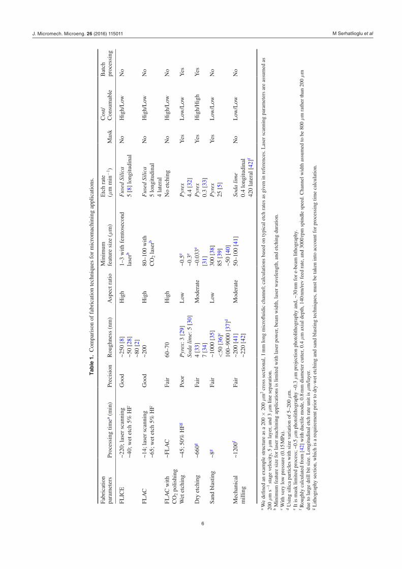
in x direction in fused silica sample for given microfluidic channels in figure 5. The two channels shown in figure 5(a) are fabricated using the same FLAC parameters. The top channel shown in figure 5(b) was left unprocessed whereas the bottom channel shown in figure 5(c) went through an addi-tional CO2 laser polishing step. The untreated channel looks hazy; in comparison, the CO2 laser polished channels look transparent. Figures 5(b) and (c) report 20× magnified optical microscope images in order to compare unpolished and pol-ished microfluidic channels. During the CO2 laser treatment step, the micro-pits are melted, solidified and expanded to the entire surface.
We have also prepared a microfluidic test chip in order to demonstrate the performance of these two channels for optical imaging. The two channels shown in figure 5 were bonded to a rectangular fused silica substrate. In order to achieve a leak-free and high quality bonding, the contact surfaces must be clean and as smooth as possible. Although FLAC process has high etching selectivity between femtosecond laser radi-ated and non-radiated areas, keeping fused silica samples in high concentrations of the HF solution for longer increases the surface roughness. Moreover, the CO2 laser direct radiation to the outside of microwell pattern on glass surface (due to a lack of precision in the CO2 laser stage) can cause higher surface roughness which prevents glass-to-glass bonding. Therefore, HF acid interaction time, CO2 laser power, and the CO2 laser scanning area must be precisely adjusted.
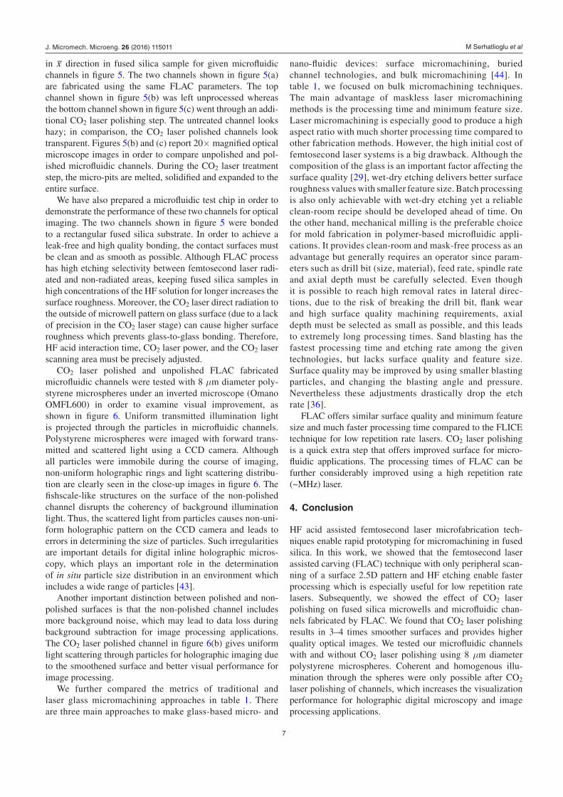
CO2 laser polished and unpolished FLAC fabricated microfluidic channels were tested with 8 µm diameter poly-styrene microspheres under an inverted microscope (Omano OMFL600) in order to examine visual improvement, as shown in figure 6. Uniform transmitted illumination light is projected through the particles in microfluidic channels. Polystyrene microspheres were imaged with forward trans-mitted and scattered light using a CCD camera. Although all particles were immobile during the course of imaging, non-uniform holographic rings and light scattering distribu-tion are clearly seen in the close-up images in figure 6. The fishscale-like structures on the surface of the non-polished channel disrupts the coherency of background illumination light. Thus, the scattered light from particles causes non-uni-form holographic pattern on the CCD camera and leads to errors in determining the size of particles. Such irregularities are important details for digital inline holographic micros-copy, which plays an important role in the determination of in situ particle size distribution in an environment which includes a wide range of particles [43].
Another important distinction between polished and non-polished surfaces is that the non-polished channel includes more background noise, which may lead to data loss during background subtraction for image processing applications. The CO2 laser polished channel in figure 6(b) gives uniform light scattering through particles for holographic imaging due to the smoothened surface and better visual performance for image processing.
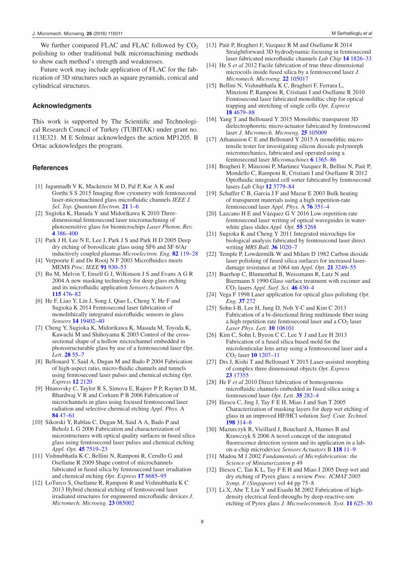
We further compared the metrics of traditional and laser glass micromachining approaches in table 1. There are three main approaches to make glass-based micro- and
nano-fluidic devices: surface micromachining, buried channel technologies, and bulk micromachining [44]. In table 1, we focused on bulk micromachining techniques. The main advantage of maskless laser micromachining methods is the processing time and minimum feature size. Laser micromachining is especially good to produce a high aspect ratio with much shorter processing time compared to other fabrication methods. However, the high initial cost of femtosecond laser systems is a big drawback. Although the composition of the glass is an important factor affecting the surface quality [29], wet-dry etching delivers better surface roughness values with smaller feature size. Batch processing is also only achievable with wet-dry etching yet a reliable clean-room recipe should be developed ahead of time. On the other hand, mechanical milling is the preferable choice for mold fabrication in polymer-based microfluidic appli-cations. It provides clean-room and mask-free process as an advantage but generally requires an operator since param-eters such as drill bit (size, material), feed rate, spindle rate and axial depth must be carefully selected. Even though it is possible to reach high removal rates in lateral direc-tions, due to the risk of breaking the drill bit, flank wear and high surface quality machining requirements, axial depth must be selected as small as possible, and this leads to extremely long processing times. Sand blasting has the fastest processing time and etching rate among the given technologies, but lacks surface quality and feature size. Surface quality may be improved by using smaller blasting particles, and changing the blasting angle and pressure. Nevertheless these adjustments drastically drop the etch rate [36].
FLAC offers similar surface quality and minimum feature size and much faster processing time compared to the FLICE technique for low repetition rate lasers. CO2 laser polishing is a quick extra step that offers improved surface for micro-fluidic applications. The processing times of FLAC can be further considerably improved using a high repetition rate (~MHz) laser.
4. Conclusion
HF acid assisted femtosecond laser microfabrication tech-niques enable rapid prototyping for micromachining in fused silica. In this work, we showed that the femtosecond laser assisted carving (FLAC) technique with only peripheral scan-ning of a surface 2.5D pattern and HF etching enable faster processing which is especially useful for low repetition rate lasers. Subsequently, we showed the effect of CO2 laser polishing on fused silica microwells and microfluidic chan-nels fabricated by FLAC. We found that CO2 laser polishing results in 3–4 times smoother surfaces and provides higher quality optical images. We tested our microfluidic channels with and without CO2 laser polishing using 8 µm diameter polystyrene microspheres. Coherent and homogenous illu-mination through the spheres were only possible after CO2 laser polishing of channels, which increases the visualization performance for holographic digital microscopy and image processing applications.
J. Micromech. Microeng. 26 (2016) 115011
M Serhatlioglu et al
8
We further compared FLAC and FLAC followed by CO2 polishing to other traditional bulk micromachining methods to show each method’s strength and weaknesses.
Future work may include application of FLAC for the fab-rication of 3D structures such as square pyramids, conical and cylindrical structures.
Acknowledgments
This work is supported by The Scientific and Technologi-cal Research Council of Turkey (TUBITAK) under grant no. 113E321. M E Solmaz acknowledges the action MP1205. B Ortac acknowledges the program.
References
[1] Jagannadh V K, Mackenzie M D, Pal P, Kar A K and Gorthi S S 2015 Imaging flow cytometry with femtosecond laser-micromachined glass microfluidic channels IEEE J. Sel. Top. Quantum Electron. 21 1–6
[2] Sugioka K, Hanada Y and Midorikawa K 2010 Three-dimensional femtosecond laser micromachining of photosensitive glass for biomicrochips Laser Photon. Rev. 4 386–400
[3] Park J H, Lee N E, Lee J, Park J S and Park H D 2005 Deep dry etching of borosilicate glass using SF6 and SF 6/Ar inductively coupled plasmas Microelectron. Eng. 82 119–28
[4] Verpoorte E and De Rooij N F 2003 Microfluidics meets MEMS Proc. IEEE 91 930–53
[5] Bu M, Melvin T, Ensell G J, Wilkinson J S and Evans A G R 2004 A new masking technology for deep glass etching and its microfluidic application Sensors Actuators A 115 476–82
[6] He F, Liao Y, Lin J, Song J, Qiao L, Cheng Y, He F and Sugioka K 2014 Femtosecond laser fabrication of monolithically integrated microfluidic sensors in glass Sensors 14 19402–40
[7] Cheng Y, Sugioka K, Midorikawa K, Masuda M, Toyoda K, Kawachi M and Shihoyama K 2003 Control of the cross-sectional shape of a hollow microchannel embedded in photostructurable glass by use of a femtosecond laser Opt. Lett. 28 55–7
[8] Bellouard Y, Said A, Dugan M and Bado P 2004 Fabrication of high-aspect ratio, micro-fluidic channels and tunnels using femtosecond laser pulses and chemical etching Opt. Express 12 2120
[9] Hnatovsky C, Taylor R S, Simova E, Rajeev P P, Rayner D M, Bhardwaj V R and Corkum P B 2006 Fabrication of microchannels in glass using focused femtosecond laser radiation and selective chemical etching Appl. Phys. A 84 47–61
[10] Sikorski Y, Rablau C, Dugan M, Said A A, Bado P and Beholz L G 2006 Fabrication and characterization of microstructures with optical quality surfaces in fused silica glass using femtosecond laser pulses and chemical etching Appl. Opt. 45 7519–23
[11] Vishnubhatla K C, Bellini N, Ramponi R, Cerullo G and Osellame R 2009 Shape control of microchannels fabricated in fused silica by femtosecond laser irradiation and chemical etching Opt. Express 17 8685–95
[12] LoTurco S, Osellame R, Ramponi R and Vishnubhatla K C 2013 Hybrid chemical etching of femtosecond laser irradiated structures for engineered microfluidic devices J. Micromech. Microeng. 23 085002
[13] Paiè P, Bragheri F, Vazquez R M and Osellame R 2014 Straightforward 3D hydrodynamic focusing in femtosecond laser fabricated microfluidic channels Lab Chip 14 1826–33
[14] He S et al 2012 Facile fabrication of true three-dimensional microcoils inside fused silica by a femtosecond laser J. Micromech. Microeng. 22 105017
[15] Bellini N, Vishnubhatla K C, Bragheri F, Ferrara L, Minzioni P, Ramponi R, Cristiani I and Osellame R 2010 Femtosecond laser fabricated monolithic chip for optical trapping and stretching of single cells Opt. Express 18 4679–88
[16] Yang T and Bellouard Y 2015 Monolithic transparent 3D dielectrophoretic micro-actuator fabricated by femtosecond laser J. Micromech. Microeng. 25 105009
[17] Athanasiou C E and Bellouard Y 2015 A monolithic micro-tensile tester for investigating silicon dioxide polymorph micromechanics, fabricated and operated using a femtosecond laser Micromachines 6 1365–86
[18] Bragheri F, Minzioni P, Martinez Vazquez R, Bellini N, Paiè P, Mondello C, Ramponi R, Cristiani I and Osellame R 2012 Optofluidic integrated cell sorter fabricated by femtosecond lasers Lab Chip 12 3779–84
[19] Schaffer C B, Garcia J F and Mazur E 2003 Bulk heating of transparent materials using a high repetition-rate femtosecond laser Appl. Phys. A 76 351–4
[20] Lazcano H E and Vázquez G V 2016 Low-repetition rate femtosecond laser writing of optical waveguides in water-white glass slides Appl. Opt. 55 3268
[21] Sugioka K and Cheng Y 2011 Integrated microchips for biological analysis fabricated by femtosecond laser direct writing MRS Bull. 36 1020–7
[22] Temple P, Lowdermilk W and Milam D 1982 Carbon dioxide laser polishing of fused silica surfaces for increased laser-damage resistance at 1064 nm Appl. Opt. 21 3249–55
[23] Buerhop C, Blumenthal B, Weissmann R, Lutz N and Biermann S 1990 Glass surface treatment with excimer and CO2 lasers Appl. Surf. Sci. 46 430–4
[24] Vega F 1998 Laser application for optical glass polishing Opt. Eng. 37 272
[25] Sohn I-B, Lee H, Jung D, Noh Y-C and Kim C 2013 Fabrication of a bi-directional firing multimode fiber using a high repetition rate femtosecond laser and a CO2 laser Laser Phys. Lett. 10 106101
[26] Kim C, Sohn I, Byeon C C, Lee Y J and Lee H 2013 Fabrication of a fused silica based mold for the microlenticular lens array using a femtosecond laser and a CO2 laser 10 1207–11
[27] Drs J, Kishi T and Bellouard Y 2015 Laser-assisted morphing of complex three dimensional objects Opt. Express 23 17355
[28] He F et al 2010 Direct fabrication of homogeneous microfluidic channels embedded in fused silica using a femtosecond laser Opt. Lett. 35 282–4
[29] Iliescu C, Jing J, Tay F E H, Miao J and Sun T 2005 Characterization of masking layers for deep wet etching of glass in an improved HF/HCl solution Surf. Coat. Technol. 198 314–8
[30] Mazurczyk R, Vieillard J, Bouchard A, Hannes B and Krawczyk S 2006 A novel concept of the integrated fluorescence detection system and its application in a lab-on-a-chip microdevice Sensors Actuators B 118 11–9
[31] Madou M J 2002 Fundamentals of Microfabrication: the Science of Miniaturization p 49
[32] Iliescu C, Tan K L, Tay F E H and Miao J 2005 Deep wet and dry etching of Pyrex glass: a review Proc. ICMAT 2005 Symp. F (Singapore) vol 44 pp 75–8
[33] Li X, Abe T, Liu Y and Esashi M 2002 Fabrication of high-density electrical feed-throughs by deep-reactive-ion etching of Pyrex glass J. Microelectromech. Syst. 11 625–30
J. Micromech. Microeng. 26 (2016) 115011
M Serhatlioglu et al
9
[34] Ichiki T, Sugiyama Y, Taura R, Koidesawa T and Horiike Y 2003 Plasma applications for biochip technology Thin Solid Films 435 62–8
[35] Guijt R M, Baltussen E, van der Steen G, Schasfoort R B M, Schlautmann S, Billiet H A H, Frank J, van Dedem G W K and van den Berg A 2001 New approaches for fabrication of microfluidic capillary electrophoresis devices with on-chip conductivity detection Electrophoresis 22 235–41
[36] Mineta T, Takada T, Makino E, Kawashima T and Shibata T 2008 A wet abrasive blasting process for smooth micromachining of glass by ductile-mode removal J. Micromech. Microeng. 19 015031
[37] Slikkerveer P J, Bouten P C P and De Haas F C M 2000 High quality mechanical etching of brittle materials by powder blasting Sensors Actuators A 85 296–303
[38] Plaza J A, Lopez M J, Moreno A, Duch M and Cane C 2003 Definition of high aspect ratio glass columns Sensors Actuators A 105 305–10
[39] Schlautmann S, Wensink H, Schasfoort R, Elwenspoek M and Van Den Berg A 2001 Powder-blasting technology
as an alternative tool for microfabrication of capillary electrophoresis chips with integrated conductivity sensors J. Micromech. Microeng. 11 386–9
[40] Wensink H, Berenschot J W, Jansen H V and Elwenspoek M C 2000 High resolution powder blast micromachining Proc. IEEE 13th Annual Int. Conf. Micro Electro Mechanical Systems (Cat. No.00CH36308) pp 769–74
[41] Abgrall P and Gué A-M 2007 Lab-on-chip technologies: making a microfluidic network and coupling it into a complete microsystem—a review J. Micromech. Microeng. 17 R15–49
[42] Arif M, Rahman M and San W Y 2011 Ultraprecision ductile mode machining of glass by micromilling process J. Manuf. Process. 13 50–9
[43] Davies E J, Nimmo-Smith W A M, Agrawal Y C and Souza A J 2011 Scattering signatures of suspended particles: an integrated system for combining digital holography and laser diffraction Opt. Express 19 25488–99
[44] Iliescu C, Taylor H, Avram M, Miao J and Franssila S 2012 A practical guide for the fabrication of microfluidic devices using glass and silicon Biomicrofluidics 6 16505
J. Micromech. Microeng. 26 (2016) 115011