Embed Size (px)
Citation preview
Luigi ColomboTexas Instruments Incorporated
Dallas, TX, USA
G h C f F R h t A li tiGraphene Conference: From Research to Applications15-16 Oct 2012
NPL,UKNPL,UK

UT Austin - Banerjee group UT Austin Banerjee group UT Austin - Tutuc group UT Austin – Ruoff UT Austin Ruoff UT Dallas - Wallace group UT Dallas J Kim group UT Dallas - J. Kim group GIT/UT Dallas – Vogel group
Nano-electronic Research Initiative and NIST
NPL Teddington 15-16 Oct 2012 LColombo

Introduction Introduction Graphene based devices Graphene integration Graphene integration
Graphene film growth Dielectrics – thickness scalinggMetal contacts – contact resistance
Summaryy
NPL Teddington 15-16 Oct 2012 LColombo
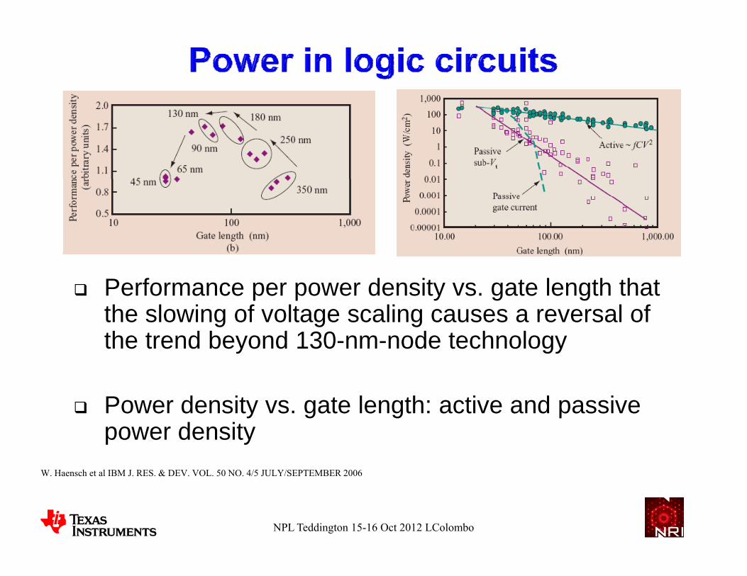
Performance per power density vs. gate length that the slowing of voltage scaling causes a reversal of g g gthe trend beyond 130-nm-node technology
P d it t l th ti d i Power density vs. gate length: active and passive power density
h l S & O 0 O 4/ /S 2006
NPL Teddington 15-16 Oct 2012 LColombo
W. Haensch et al IBM J. RES. & DEV. VOL. 50 NO. 4/5 JULY/SEPTEMBER 2006
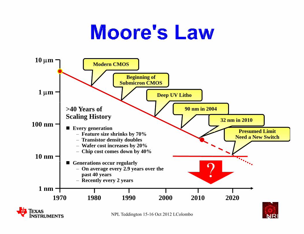
Modern CMOS10 m
Beginning ofSubmicron CMOS
Deep UV Litho1 m
90 nm in 2004
Presumed Limit100 nm
>40 Years of Scaling History Every generation
32 nm in 2010
Presumed LimitNeed a New Switch
10 nm
– Feature size shrinks by 70%– Transistor density doubles– Wafer cost increases by 20%– Chip cost comes down by 40%
G ti l l
1 nm
Generations occur regularly– On average every 2.9 years over the
past 40 years– Recently every 2 years
?
NPL Teddington 15-16 Oct 2012 LColombo
1970 1980 1990 2000 2010 2020
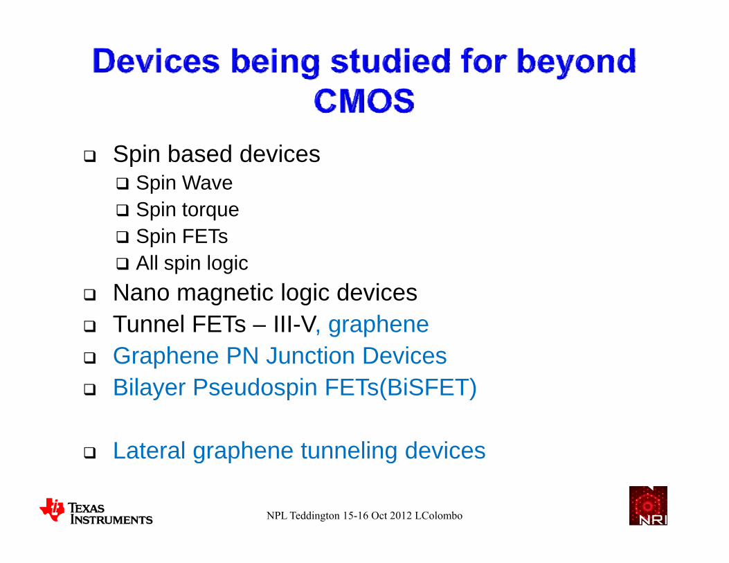
Spin based devicesS i W Spin Wave
Spin torque Spin FETsp All spin logic
Nano magnetic logic devicesT l FET III V h Tunnel FETs – III-V, graphene
Graphene PN Junction Devices Bilayer Pseudospin FETs(BiSFET) Bilayer Pseudospin FETs(BiSFET)
Lateral graphene tunneling devicesg p g
NPL Teddington 15-16 Oct 2012 LColombo
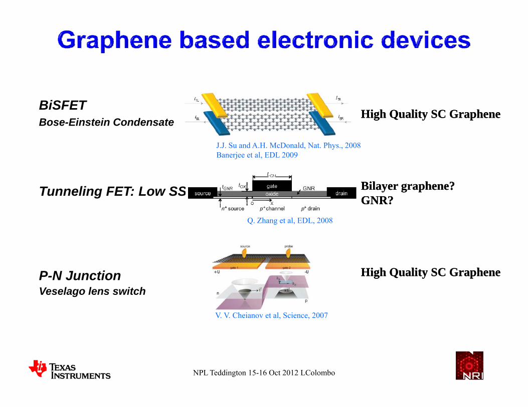
BiSFET• Bose-Einstein Condensate
High Quality SC GrapheneHigh Quality SC Graphene
J.J. Su and A.H. McDonald, Nat. Phys., 2008Banerjee et al, EDL 2009
Tunneling FET: Low SS
Q. Zhang et al, EDL, 2008
BilayerBilayer graphene?graphene?GNR?GNR?
P-N Junction High Quality SC GrapheneHigh Quality SC Graphene• Veselago lens switch
V. V. Cheianov et al, Science, 2007
NPL Teddington 15-16 Oct 2012 LColombo
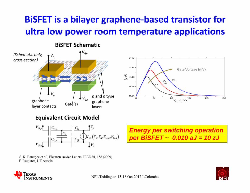
BiSFET SchematicVGnVn(Schematic only,
cross section)cross‐section)
Gate Voltage (mV)
VGp
Vp p and n type graphene layers
graphene layer contacts Gate(s)
Equivalent Circuit Model
y
Energy per switching operation gy p g pper BiSFET ~ 0.010 aJ = 10 zJ
S K Banerjee et al Electron Device Letters IEEE 30 158 (2009)
NPL Teddington 15-16 Oct 2012 LColombo
F. Register, UT AustinS. K. Banerjee et al., Electron Device Letters, IEEE 30, 158 (2009).
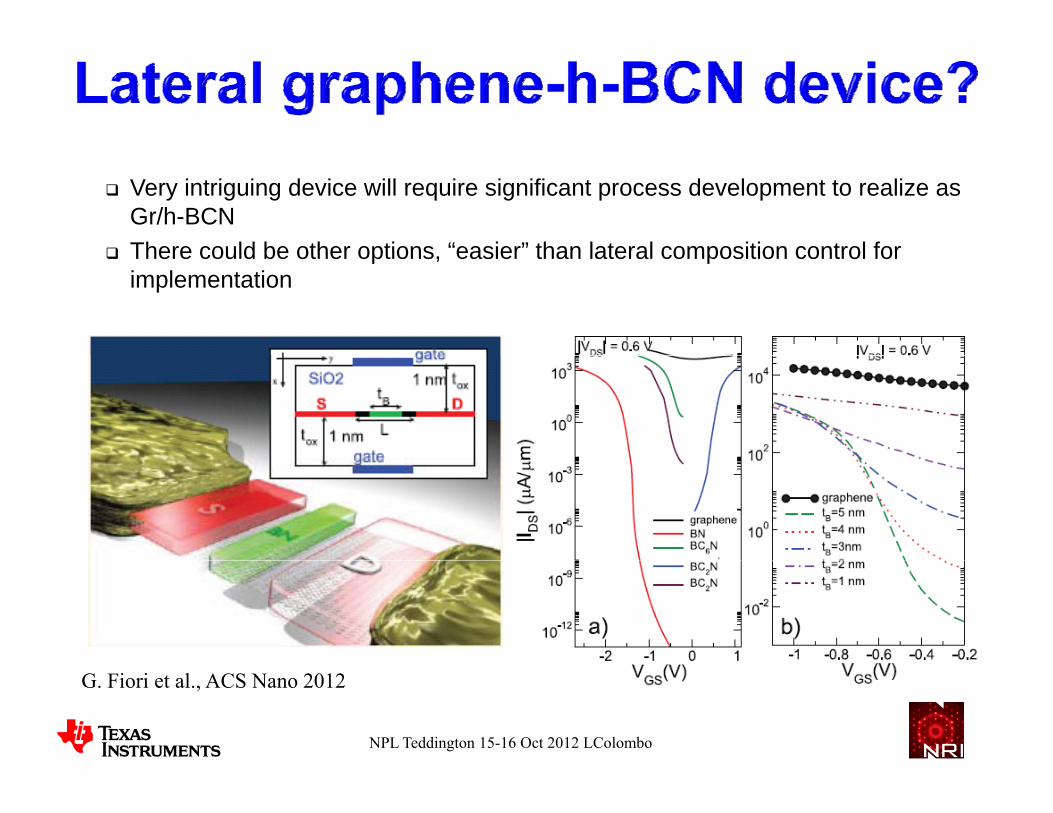
Very intriguing device will require significant process development to realize as Gr/h-BCN
There could be other options “easier” than lateral composition control for There could be other options, easier than lateral composition control for implementation
NPL Teddington 15-16 Oct 2012 LColombo
G. Fiori et al., ACS Nano 2012
Graphene Growth Monolayer graphene Graphene nano ribbons (GNR)LER is a major challenge for etched GNRsChemical pathways for growing GNRs – placement
challenge Bi-layer graphene Bi-layer grapheneChemically inactive graphene surface is a major challenge
for uniform bi-layer growth Surface modification – e.g.: BCN
Dielectric selection and deposition High-k – scaling Low-k - scaling Lattice matched – 2D crystals
M t l t t
NPL Teddington 15-16 Oct 2012 LColombo
Metal contacts
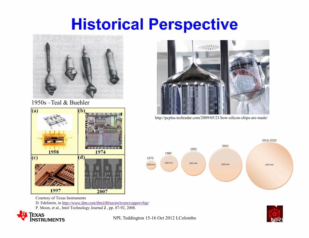
1950s –Teal & Buehler1950s Teal & Buehler
http://pcplus.techradar.com/2009/05/21/how-silicon-chips-are-made/
Courtesy of Texas InstrumentsD. Edelstein, in http://www.ibm.com/ibm100/us/en/icons/copperchip/P. Moon, et al., Intel Technology Journal 2 , pp. 87-92, 2008.
NPL Teddington 15-16 Oct 2012 LColombo
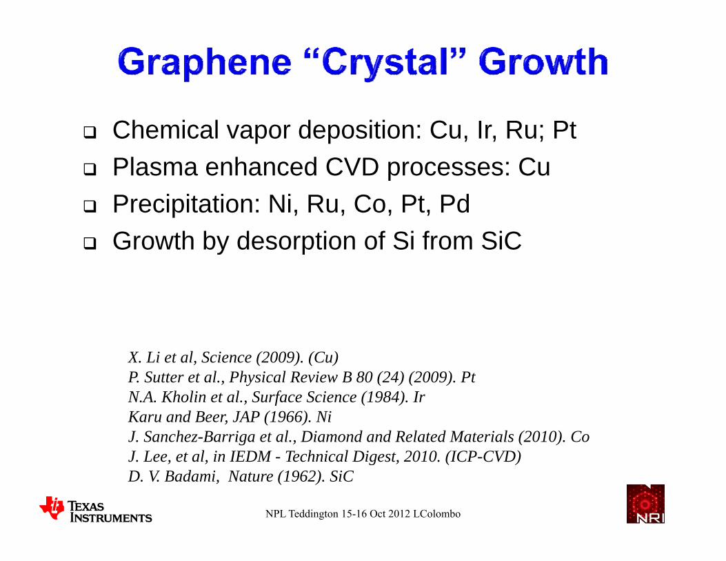
Chemical vapor deposition: Cu, Ir, Ru; Pt Plasma enhanced CVD processes: Cu Plasma enhanced CVD processes: Cu Precipitation: Ni, Ru, Co, Pt, Pd Growth by desorption of Si from SiC Growth by desorption of Si from SiC
X. Li et al, Science (2009). (Cu)P. Sutter et al., Physical Review B 80 (24) (2009). PtN.A. Kholin et al., Surface Science (1984). IrKaru and Beer, JAP (1966). NiJ. Sanchez-Barriga et al., Diamond and Related Materials (2010). CoJ Lee et al in IEDM - Technical Digest 2010 (ICP-CVD)
NPL Teddington 15-16 Oct 2012 LColombo
J. Lee, et al, in IEDM - Technical Digest, 2010. (ICP-CVD)D. V. Badami, Nature (1962). SiC
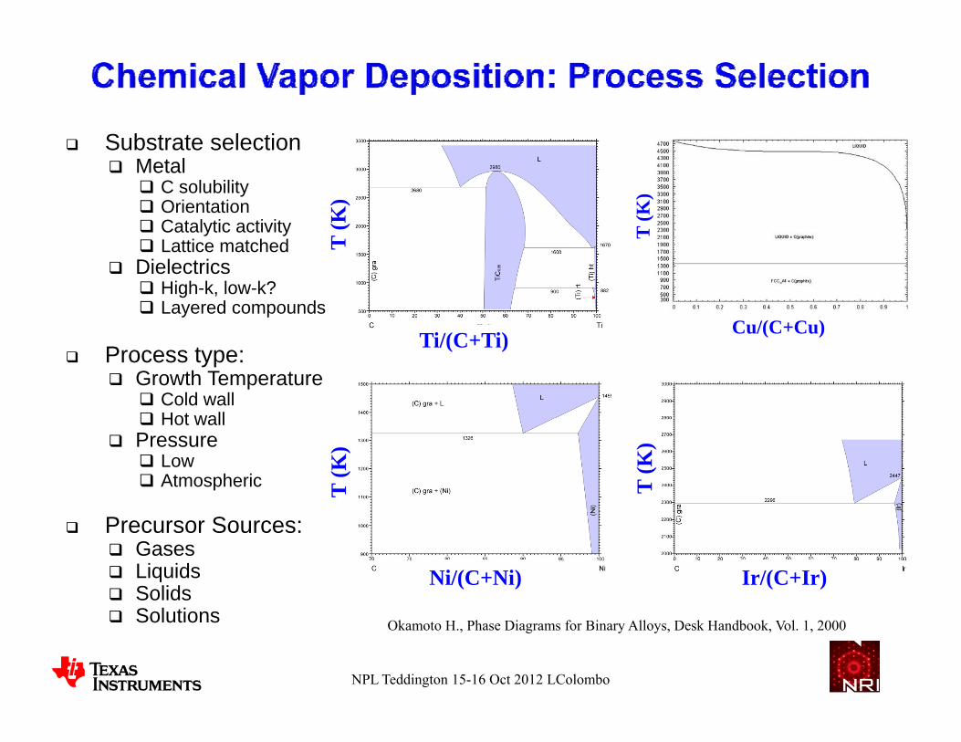
S b t t l ti Substrate selection Metal C solubility Orientation Catalytic activity T
(K)
(K)
Catalytic activity Lattice matched
Dielectrics High-k, low-k? Layered compounds
C /(C+C )
TT Process type:
Growth Temperature Cold wall Hot wall
Cu/(C+Cu)Ti/(C+Ti)
Hot wall Pressure Low Atmospheric T
(K)
T (K
)
Precursor Sources: Gases Liquids Solids
Ni/(C+Ni) Ir/(C+Ir)
Solutions
NPL Teddington 15-16 Oct 2012 LColombo
Okamoto H., Phase Diagrams for Binary Alloys, Desk Handbook, Vol. 1, 2000
We can grow large area graphene
Large area low defect density single crystals of graphene are g y g y g pmost likely required to achieve the highest uniform transport properties for nano-electronic devices
Can large single crystals of graphene be grown? Do we have the right substrate? Is the growth rate high enough for commercial viability?
2-D growth from a single nucleus?
Can “registered” nuclei of graphene be created for further graphene large area crystal growth?
NPL Teddington 15-16 Oct 2012 LColombo

TEMSEM
graphene
20 m
Cu Graphene
10
G p e eislands
Cu5 m10 m G. B.
erag
e (%
)
75
100
Li et at. Science, 2009ur
face
Cov
e
25
50
75140 mTorr 285 mTorr 560 mTorr
Q. Yu et al., Nature Materials, 2011
Time (min)0 1 2 3 4 5
Cu
Su
0
NPL Teddington 15-16 Oct 2012 LColombo
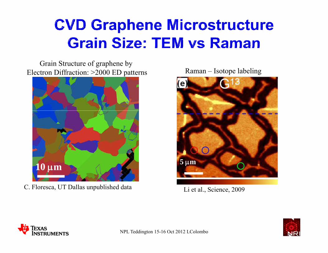
Grain Structure of graphene by Electron Diffraction: >2000 ED patterns Raman – Isotope labeling
5 m10 m
C. Floresca, UT Dallas unpublished data Li et al., Science, 2009
NPL Teddington 15-16 Oct 2012 LColombo
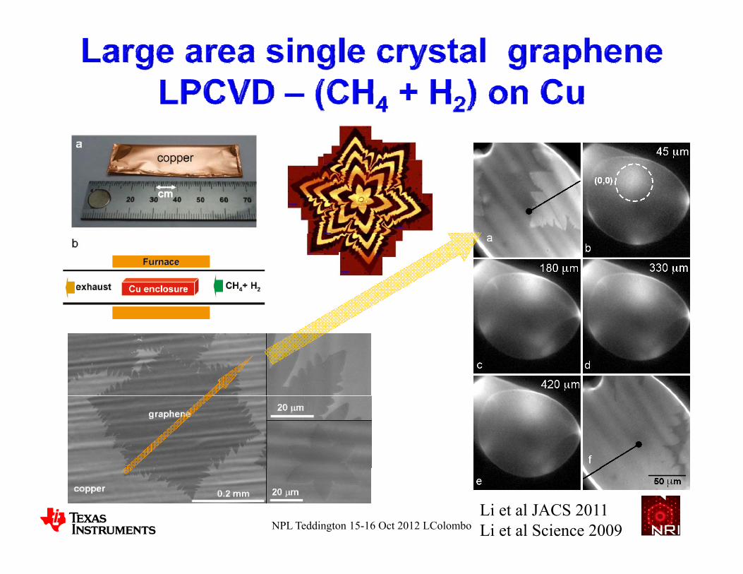
NPL Teddington 15-16 Oct 2012 LColomboLi et al., JACS 2011Li et al JACS 2011
Li et al Science 2009

Cu substrate Pt substrate
400 m
Yan Z, ACS Nano 2012
1 mmL. Gao et al Nat. Comm. (2012)Y.Hao Unpublished results – UT Austin
NPL Teddington 15-16 Oct 2012 LColombo
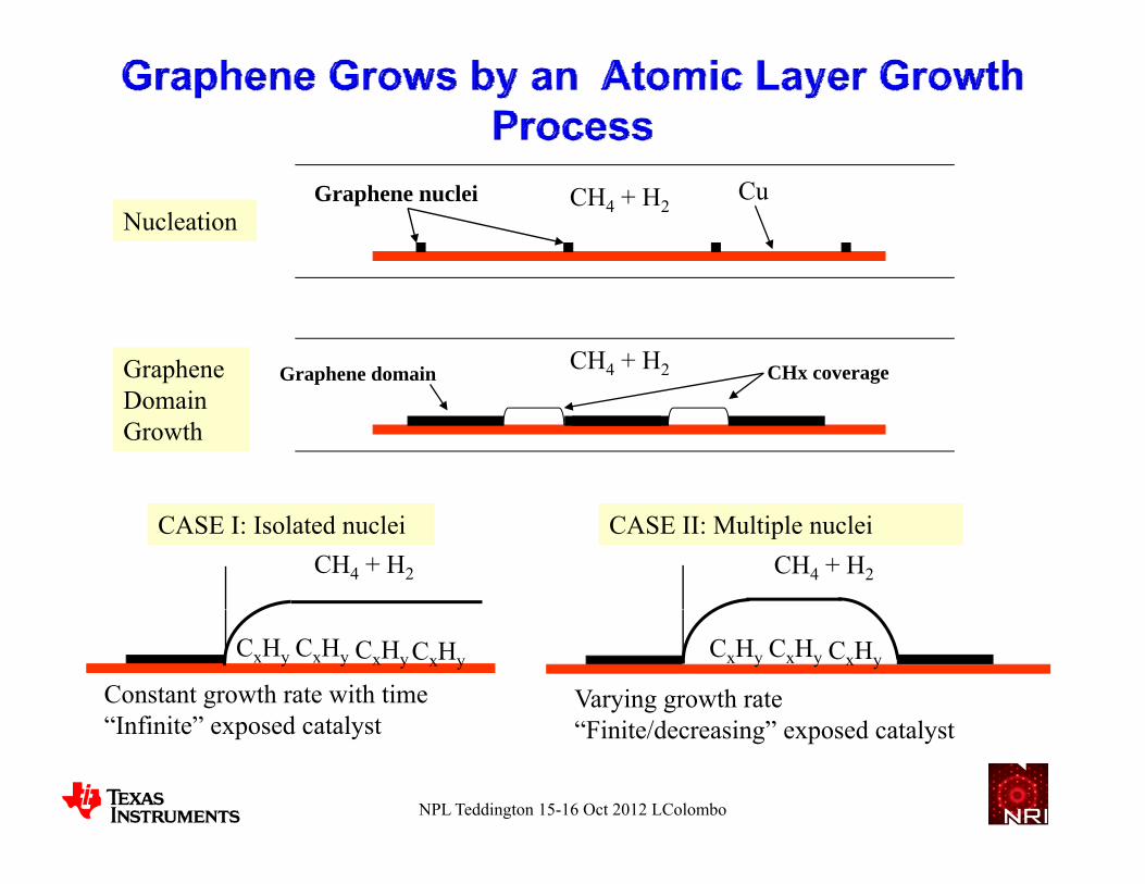
NucleationCH4 + H2Graphene nuclei Cu
Graphene CH4 + H2Graphene domain CHx coverageDomainGrowth
CH4 + H2
CASE I: Isolated nucleiCH4 + H2
CASE II: Multiple nuclei
CxHy CxHy CxHy CxHy CxHy CxHy CxHy
Constant growth rate with time“I fi it ” d t l t
Varying growth rate“ i i /d i ” d l
NPL Teddington 15-16 Oct 2012 LColombo
“Infinite” exposed catalyst “Finite/decreasing” exposed catalyst
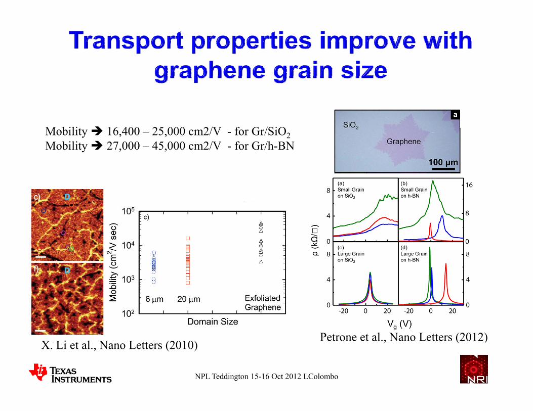
M bili 16 400 25 000 2/V f G /SiOMobility 16,400 – 25,000 cm2/V - for Gr/SiO2Mobility 27,000 – 45,000 cm2/V - for Gr/h-BN
P t t l N L tt (2012)
NPL Teddington 15-16 Oct 2012 LColombo
X. Li et al., Nano Letters (2010)Petrone et al., Nano Letters (2012)

Very large area graphene can be grown on Cu and transferred to any substrate.
PMMA Fe3+
AAcetone
Si/SiO2 Si/SiO2
NPL Teddington 15-16 Oct 2012 LColombo
Li et al,. Nano Lett (2009) Bae et al. Nat. Nanotech. (2010)
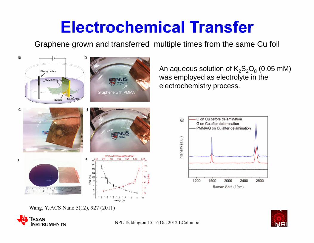
Graphene grown and transferred multiple times from the same Cu foilGraphene grown and transferred multiple times from the same Cu foil
An aqueous solution of K2S2O8 (0.05 mM) l d l t l t i thwas employed as electrolyte in the
electrochemistry process.
NPL Teddington 15-16 Oct 2012 LColombo
Wang, Y, ACS Nano 5(12), 927 (2011)
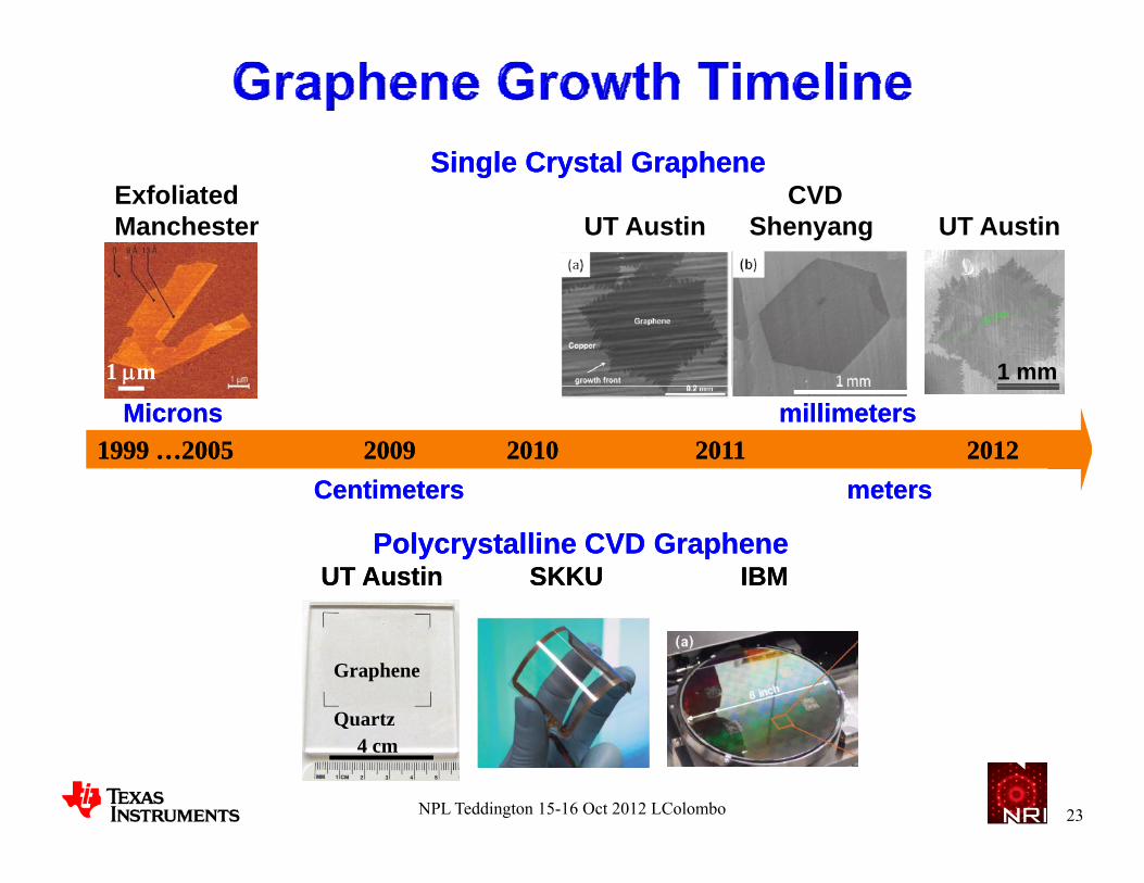
Single Crystal GrapheneSingle Crystal GrapheneSingle Crystal GrapheneSingle Crystal GrapheneExfoliated CVDManchester UT Austin Shenyang UT Austin
1 m 1 mm
1999 …2005 2009 1999 …2005 2009 2010 2010 2011 20122011 2012Microns millimetersMicrons millimeters
Centimeters metersCentimeters meters
Polycrystalline CVD GraphenePolycrystalline CVD GrapheneUT Austin SKKU IBMUT Austin SKKU IBM
Centimeters metersCentimeters meters
Graphene
QuartzQuartz4 cm
23NPL Teddington 15-16 Oct 2012 LColombo
Graphene surface is chemically inert
Need to functionalize the surface to deposit dielectrics using non-physical deposition techniq estechniques
Scaling of dielectrics down to ~ 1 nm needed for Scaling of dielectrics down to ~ 1 nm needed for devices
Enable a variety of dielectrics – high-k, low-k and 2D dielectrics
NPL Teddington 15-16 Oct 2012 LColombo
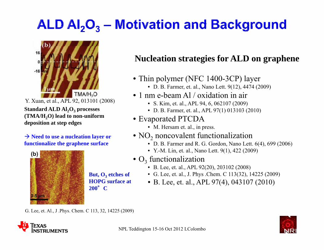
Nucleation strategies for ALD on graphene
• Thin polymer (NFC 1400 3CP) layer
Standard ALD Al O processes
• Thin polymer (NFC 1400-3CP) layer• D. B. Farmer, et. al., Nano Lett. 9(12), 4474 (2009)
• 1 nm e-beam Al / oxidation in air• S. Kim, et. al., APL 94, 6, 062107 (2009)
D B F t l APL 97(1) 013103 (2010)
Y. Xuan, et al., APL 92, 013101 (2008)Standard ALD Al2O3 processes (TMA/H2O) lead to non-uniform deposition at step edges
Need to use a nucleation layer or
• D. B. Farmer, et. al., APL 97(1) 013103 (2010)• Evaporated PTCDA
• M. Hersam et. al., in press.• NO2 noncovalent functionalization
functionalize the graphene surface • D. B. Farmer and R. G. Gordon, Nano Lett. 6(4), 699 (2006)• Y.-M. Lin, et. al., Nano Lett. 9(1), 422 (2009)
• O3 functionalization• B. Lee, et. al., APL 92(20), 203102 (2008)
G L l J Ph Ch C 113(32) 14225 (2009)• G. Lee, et. al., J. Phys .Chem. C 113(32), 14225 (2009)• B. Lee, et. al., APL 97(4), 043107 (2010)
But, O3 etches of HOPG surface at 200°C
G. Lee, et. Al., J .Phys. Chem. C 113, 32, 14225 (2009)
NPL Teddington 15-16 Oct 2012 LColombo
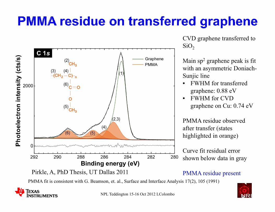
CVD graphene transferred toCVD graphene transferred to SiO2
Main sp2 graphene peak is fit i h i i hwith an asymmetric Doniach-
Sunjic line• FWHM for transferred
graphene: 0.88 eVgraphene: 0.88 eV• FWHM for CVD
graphene on Cu: 0.74 eV
PMMA id b dPMMA residue observed after transfer (states highlighted in orange)
Curve fit residual error shown below data in gray
PMMA residue presentPirkle A PhD Thesis UT Dallas 2011PMMA fit is consistent with G. Beamson, et. al., Surface and Interface Analysis 17(2), 105 (1991)
PMMA residue present
NPL Teddington 15-16 Oct 2012 LColombo
Pirkle, A, PhD Thesis, UT Dallas 2011

Al2O3 – 1 nm (nominal) Al deposited by on natural graphite by e-beam ti idi d i 1000 b O t 25°C
17 nm
evaporation,oxidized in 1000 mbar O2 at 25°C
(d)
C 1s
ty (a
.u.) O 1s Al 2p
(d) (d)
C-C
*(d) + 25°C O2
(c)
(b)
x10
on in
tens
it
(b)
(c)
(b)
(c)
Al0
(c) Unannealed natural graphite substrate + 1 nm Al
8
1 2
1 6
2 0
eigh
t (nm
)
600 nm
0 nmzRMS = 4.23 nm
(b)
x10ot
oele
ctro
(a) (a)
(b)
(a)
(b)
(a) Annealed (400°C, UHV) natural graphite
(b) + 25°C O2
• Large (~ 5-10 nm) Al clusters explain incomplete oxidation
0 1 2 30
4He
x ( m )536 532 528Ph
o
Binding energy (eV)76 72
290 286 282
natural graphite substrate + 1 nm Al
AlAl
Adsorbed H2O
(a) (b)
when pre-deposition anneal is employed• Cluster radius is larger than limiting oxide thickness
(~ 0.5 – 2 nm)1
• Further details given in Ref. 2Al2O3Al2O3
NPL Teddington 15-16 Oct 2012 LColombo
27
1. L. P. H. Jeurgens, et. al., JAP 92, 3, 1649 (2002)2. A. Pirkle, et. al, APL 95(13), 133106 (2009)
AlAdsorbed H2O
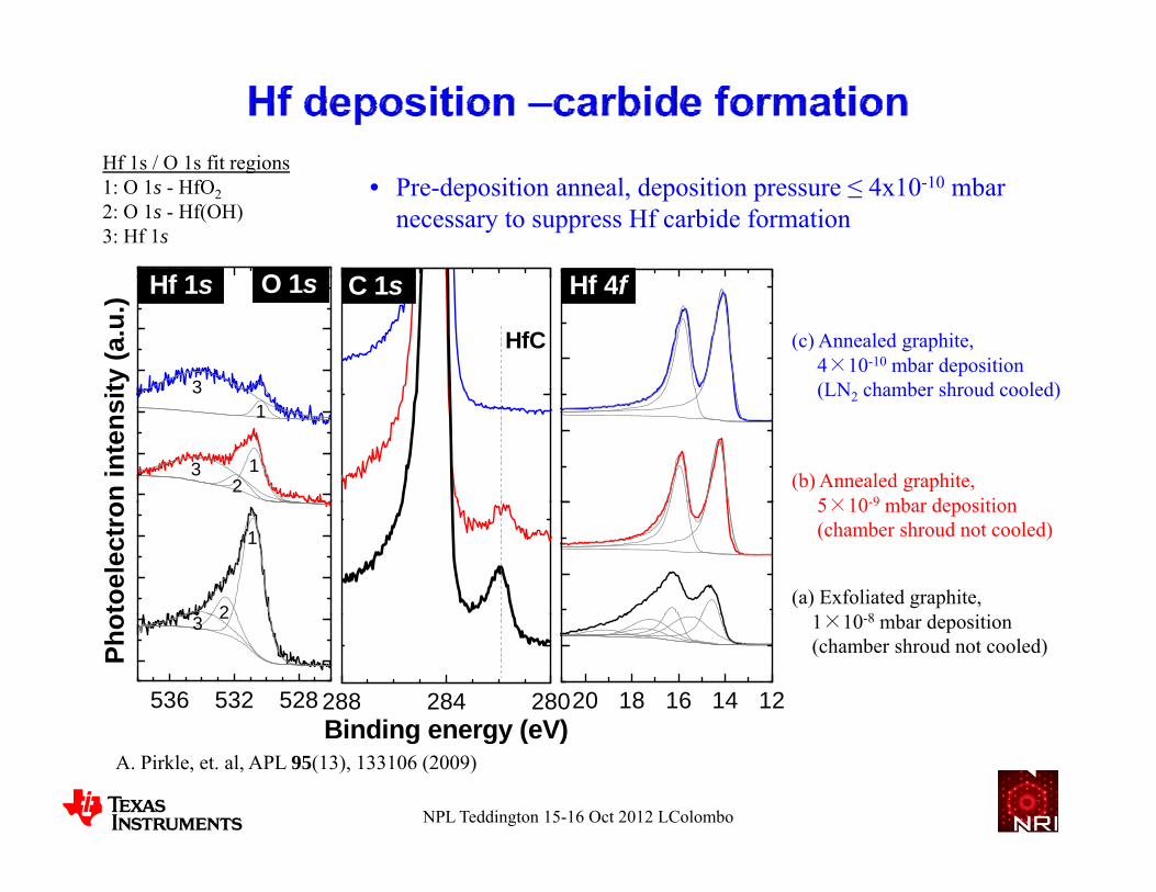
Hf 1s / O 1s fit regions• Pre-deposition anneal, deposition pressure ≤ 4x10⁻¹⁰ mbar
necessary to suppress Hf carbide formation
Hf 1s / O 1s fit regions1: O 1s - HfO22: O 1s - Hf(OH)3: Hf 1s
C 1
Hf 4fO 1Hf 1
(c) Annealed graphite, 4×10⁻¹⁰ mbar deposition(LN chamber shroud cooled)
HfC
C 1s Hf 4fO 1sHf 1s
ty (a
.u.)
3
(b) Annealed graphite, 5×10⁻⁹ mbar deposition
(LN2 chamber shroud cooled)
on in
tens
it
32
1
31
5×10⁻⁹ mbar deposition(chamber shroud not cooled)
(a) Exfoliated graphite, 1 10 8 b d i iot
oele
ctro
1
2 1×10⁻⁸ mbar deposition(chamber shroud not cooled)
288 284 280Binding energy (eV)
20 18 16 14 12536 532 528
Pho 23
Binding energy (eV) A. Pirkle, et. al, APL 95(13), 133106 (2009)
NPL Teddington 15-16 Oct 2012 LColombo

• 1 nm of HfO2 deposited on natural graphite by evaporating Hf with 1x10⁻⁶ mbar partial pressure of O2i b ti h bin e-beam evaporation chamber
• Chamber base pressure ≤ 5x10⁻¹⁰ mbar • Internal LN2 chamber shroud cooled to minimize background residual gases (OH)
ty (a
.u.) O 1s C 1s Hf 4f
1 nm HfO2 - reactive e-beam
ectr
on in
tens
it
536 532 528
Natural graphite substratePhot
oele
292 288 284 280 24 20 16 12AFM – 1 nm HfO2 on natural graphite
XPS• No carbide detected after reactive e-beam
deposition
Binding energy (eV)292 288 284 280
24 20 16 12
natural graphite•Low surface roughness:
zrms = 0.24 nm• Comparable to roughness of HfO2 on Si spectator sample
TEM – 5 nm HfO2 on natural graphite•High and low magnification i h d if itdeposition (within a factor of ~2)images show good uniformity•No pinhole/short defects observed
NPL Teddington 15-16 Oct 2012 LColombo
Pirkle, A, PhD Thesis, UT Dallas 2011
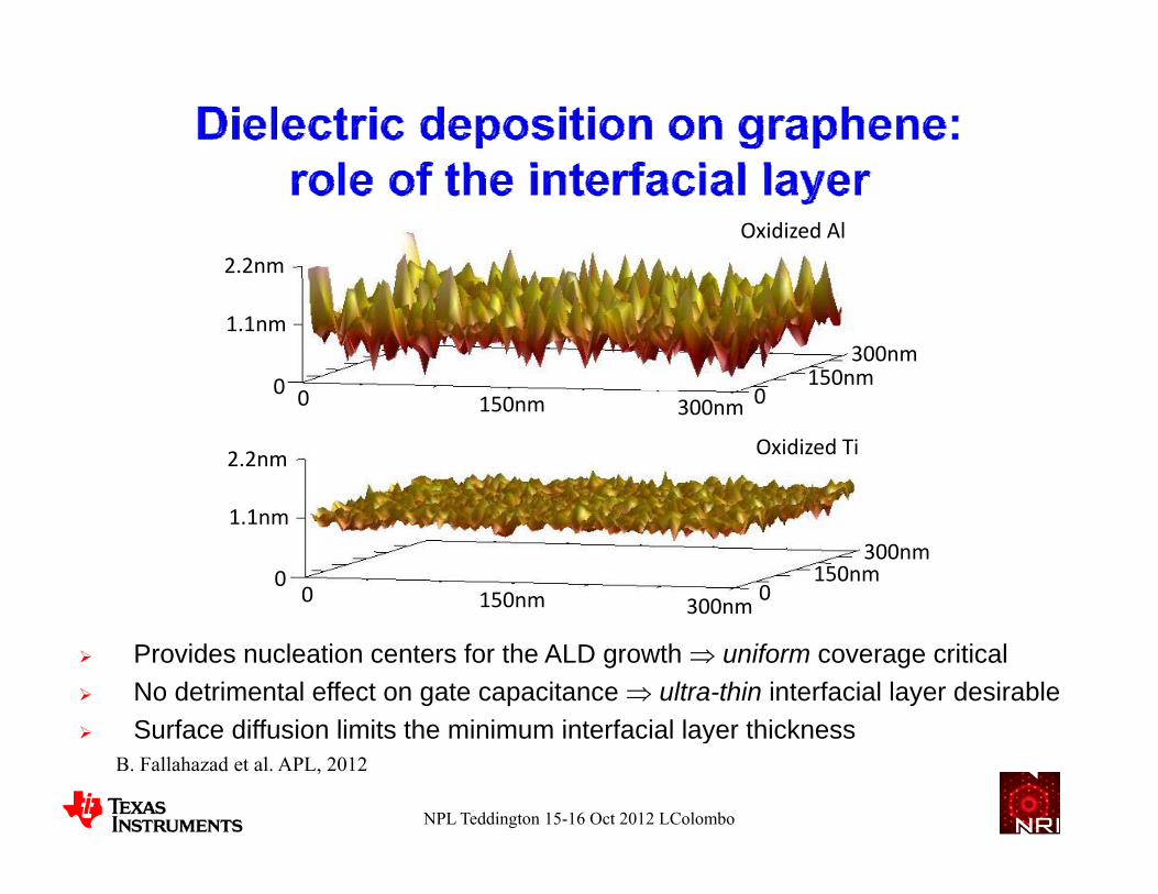
2.2nmOxidized Al
1.1nm
0 150nm300nm
00
2.2nm
0300nm150nm 00
Oxidized Ti
1.1nm
0300nm150nm
150nm300nm
00
Provides nucleation centers for the ALD growth uniform coverage critical No detrimental effect on gate capacitance ultra-thin interfacial layer desirable Surface diffusion limits the minimum interfacial layer thickness
NPL Teddington 15-16 Oct 2012 LColombo
Surface diffusion limits the minimum interfacial layer thickness B. Fallahazad et al. APL, 2012

Al O TiO dielectric on graphene scaled to 2 6nmAl2O3-TiOx dielectric on graphene scaled to ~ 2.6nm
B. Fallahazad et al APL (2012)
A id hi h k di l t i d h tAre oxide high-k dielectrics good enough to achieve high mobility in graphene?
NPL Teddington 15-16 Oct 2012 LColombo
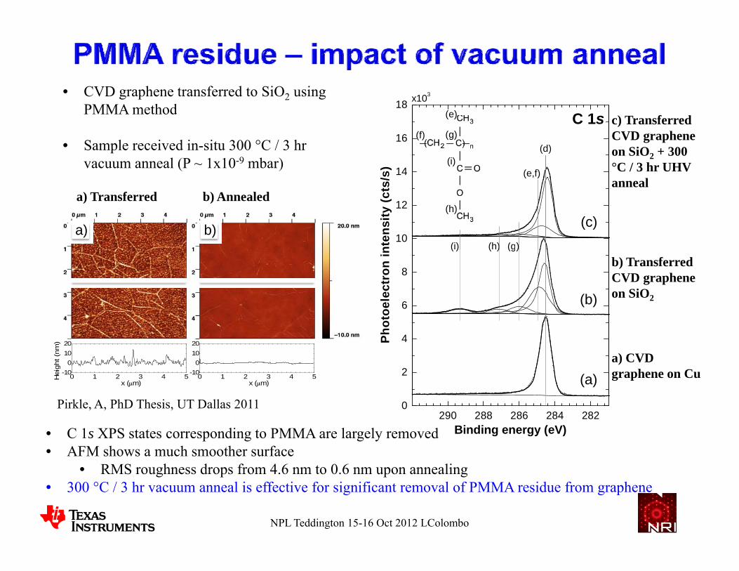
• CVD graphene transferred to SiO2 using PMMA th d 18
x103
PMMA method
• Sample received in-situ 300 °C / 3 hr vacuum anneal (P ~ 1x10⁻⁹ mbar) 14
16
18
(e,f)/s)
C 1s
(d)
(e)
(f) (g)
(i)
c) Transferred CVD graphene on SiO2 + 300 °C / 3 hr UHV
a) Transferred b) Annealed
a) b) 10
12
(i) (h) (g)
( , )
(c)
nten
sity
(cts
/
(h)
anneal
6
8
( ) ( ) (g)
(b)
otoe
lect
ron
in
b) Transferred CVD graphene on SiO2
0 1 2 3 4 5-10
01020
Hei
ght (
nm)
x ( m)0 1 2 3 4 5
-100
1020
x ( m)2
4Pho
(a)a) CVD graphene on Cu
• C 1s XPS states corresponding to PMMA are largely removed• AFM shows a much smoother surface
RMS h d f 4 6 t 0 6 li
290 288 286 284 2820
Binding energy (eV)
Pirkle, A, PhD Thesis, UT Dallas 2011
• RMS roughness drops from 4.6 nm to 0.6 nm upon annealing• 300 °C / 3 hr vacuum anneal is effective for significant removal of PMMA residue from graphene
NPL Teddington 15-16 Oct 2012 LColombo
NPL Teddington 15-16 Oct 2012 LColombo
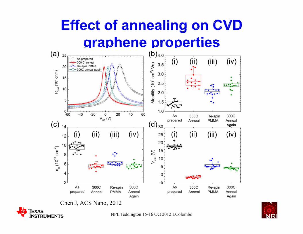
Chen J, ACS Nano, 2012
Nickel
(a) (b)
Ni/AuParylene
Ni/Au
Ni/Au Graphene5nm
5 nm
Parylene ~7 nm
SiO2
Graphene
1 um
Ni/Au
n++ Si substrate
SiO2 (90 nm)Ni/Au Graphene
3 VD= 10 mV600
Without Parylene
(a) (b)-606
nm
Mobility ~ 5000 cm2/V s
2
nce
[K
]300
400
500 sity
cps
With Parylene
0
1
Res
ista
1200 1600 2400 28000
100
200
Inte
ns
NPL Teddington 15-16 Oct 2012 LColombo
-10 0 100
VBG[V]1200 1600 2400 2800
Raman Shift (cm-1)Mordi et al., Appl. Phys. Lett. 100, 193117 (2012)
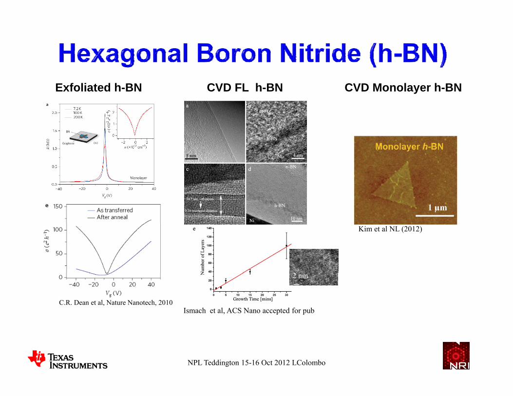
Exfoliated h-BN CVD FL h-BN CVD Monolayer h-BN
Kim et al NL (2012)
2
C.R. Dean et al, Nature Nanotech, 2010Ismach et al, ACS Nano accepted for pub
2 nm
NPL Teddington 15-16 Oct 2012 LColombo
0.5
1.0
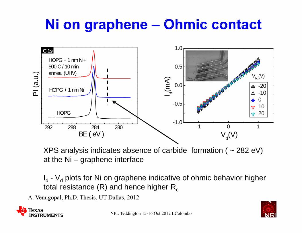
HOPG + 1 nm Ni+ 500 C / 10 min anneal (UHV))
C 1s
2 μm
0 5
0.0
I d(m
A)
-20 -100
Vbg(V)anneal (UHV)
HOPG + 1 nm NiPI (
a.u.
)
-1 0 1-1.0
-0.5 10 20
292 288 284 280( )
HOPG
• XPS analysis indicates absence of carbide formation ( ~ 282 eV) at the Ni – graphene interface
Vd(V)BE ( eV )
at the Ni graphene interface
• Id - Vd plots for Ni on graphene indicative of ohmic behavior higher total resistance (R) and hence higher Rc( ) g c
NPL Teddington 15-16 Oct 2012 LColombo
A. Venugopal, Ph.D. Thesis, UT Dallas, 2012
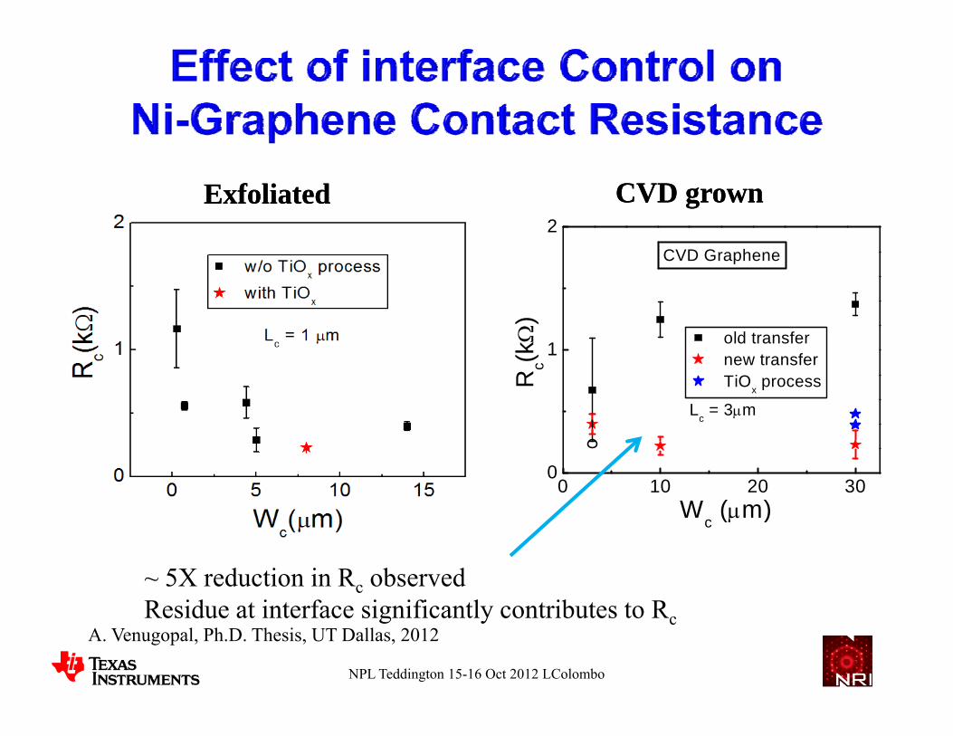
ExfoliatedExfoliated CVD grownCVD grown22
)
CVD Graphene
1 old transfer new transfer TiOx processR
c(k
)
L = 3m
0 10 20 300
W ( m)
Lc 3m
• ~ 5X reduction in Rc observedid i f i ifi l ib
Wc (m)
NPL Teddington 15-16 Oct 2012 LColombo
• Residue at interface significantly contributes to RcA. Venugopal, Ph.D. Thesis, UT Dallas, 2012
Progress has been made in graphene growth and integration of graphene-based devicesLarge area polycrystalline CVD graphene“Large”, a few mm, single crystal graphene g g y g pMany issues remain on uniformity/roughnessNeed to improve contactspScaling of dielectrics to 1 nm rangeH-BN shows promise but growth of reproducibleH BN shows promise but growth of reproducible
uniform films is still very challenging
NPL Teddington 15-16 Oct 2012 LColombo