Embed Size (px)
Citation preview
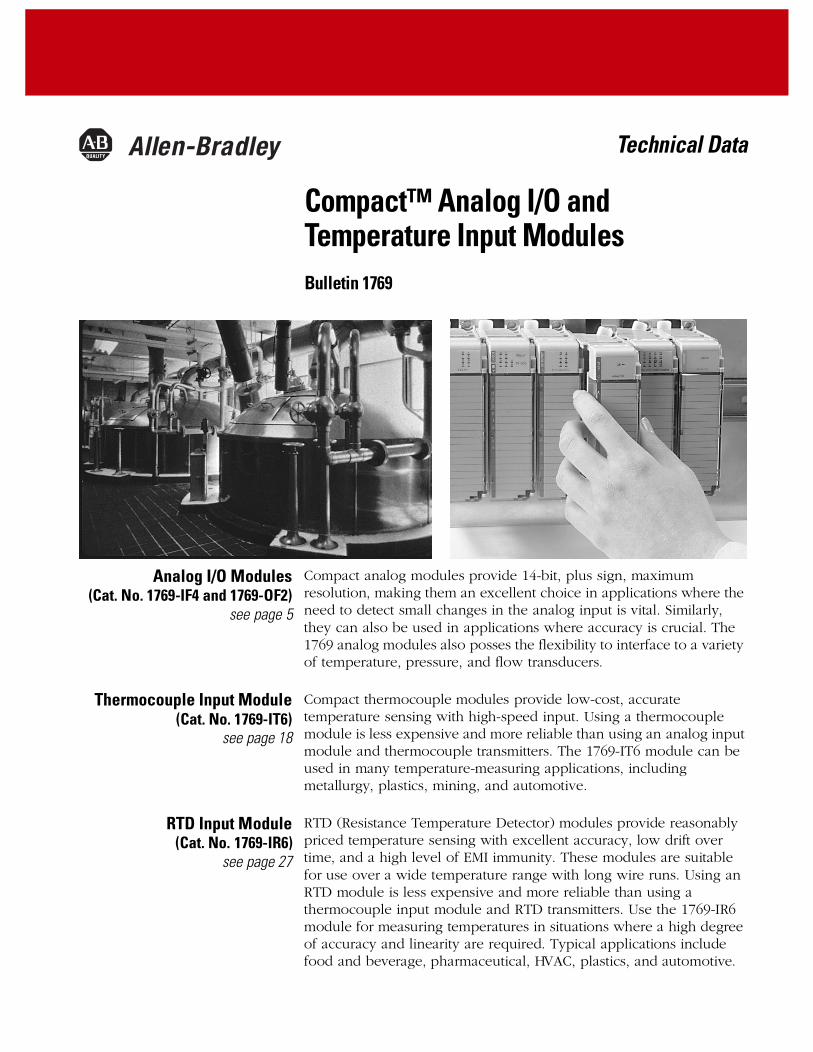
Compact™ Analog I/O and Temperature Input ModulesBulletin 1769
Technical Data
Analog I/O Modules(Cat. No. 1769-IF4 and 1769-OF2)
see page 5
Compact analog modules provide 14-bit, plus sign, maximum resolution, making them an excellent choice in applications where the need to detect small changes in the analog input is vital. Similarly, they can also be used in applications where accuracy is crucial. The 1769 analog modules also posses the flexibility to interface to a variety of temperature, pressure, and flow transducers.
Thermocouple Input Module(Cat. No. 1769-IT6)
see page 18
Compact thermocouple modules provide low-cost, accurate temperature sensing with high-speed input. Using a thermocouple module is less expensive and more reliable than using an analog input module and thermocouple transmitters. The 1769-IT6 module can be used in many temperature-measuring applications, including metallurgy, plastics, mining, and automotive.
RTD Input Module(Cat. No. 1769-IR6)
see page 27
RTD (Resistance Temperature Detector) modules provide reasonably priced temperature sensing with excellent accuracy, low drift over time, and a high level of EMI immunity. These modules are suitable for use over a wide temperature range with long wire runs. Using an RTD module is less expensive and more reliable than using a thermocouple input module and RTD transmitters. Use the 1769-IR6 module for measuring temperatures in situations where a high degree of accuracy and linearity are required. Typical applications include food and beverage, pharmaceutical, HVAC, plastics, and automotive.
2 Compact™ Analog I/O and Temperature Input Modules
1769 Compact I/O System Features and Benefits
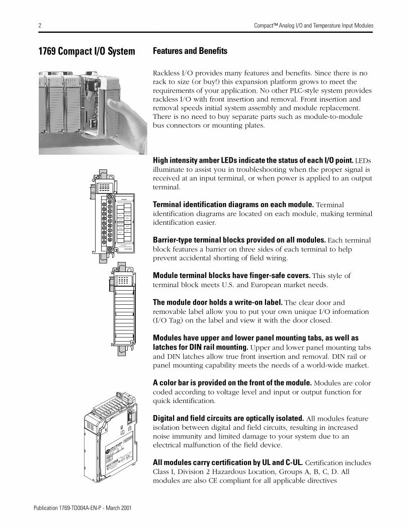
Rackless I/O provides many features and benefits. Since there is no rack to size (or buy!) this expansion platform grows to meet the requirements of your application. No other PLC-style system provides rackless I/O with front insertion and removal. Front insertion and removal speeds initial system assembly and module replacement. There is no need to buy separate parts such as module-to-module bus connectors or mounting plates.
High intensity amber LEDs indicate the status of each I/O point. LEDs illuminate to assist you in troubleshooting when the proper signal is received at an input terminal, or when power is applied to an output terminal.
Terminal identification diagrams on each module. Terminal identification diagrams are located on each module, making terminal identification easier.
Barrier-type terminal blocks provided on all modules. Each terminal block features a barrier on three sides of each terminal to help prevent accidental shorting of field wiring.
Module terminal blocks have finger-safe covers. This style of terminal block meets U.S. and European market needs.
The module door holds a write-on label. The clear door and removable label allow you to put your own unique I/O information (I/O Tag) on the label and view it with the door closed.
Modules have upper and lower panel mounting tabs, as well as latches for DIN rail mounting. Upper and lower panel mounting tabs and DIN latches allow true front insertion and removal. DIN rail or panel mounting capability meets the needs of a world-wide market.
A color bar is provided on the front of the module. Modules are color coded according to voltage level and input or output function for quick identification.
Digital and field circuits are optically isolated. All modules feature isolation between digital and field circuits, resulting in increased noise immunity and limited damage to your system due to an electrical malfunction of the field device.
All modules carry certification by UL and C-UL. Certification includes Class I, Division 2 Hazardous Location, Groups A, B, C, D. All modules are also CE compliant for all applicable directives
1769-OW8
DANGERDo Not Remove RTB Under Power
Unless Area is Non-Hazardous
Ensure AdjacentBus Lever is Unlatched/Latched Before/After Removing/Inserting Module
VAC-VDC1
OUT 3
OUT 6
OUT 0
VAC-VDC2
OUT4
OUT2
OUT 7
OUT 1
OUT 5
1769-IA 16
WIN
(21) 6
N0AA0AA Mfg
. 1298 Fac. 6
N
POWER SUPPLY D
IST. RATING 8
PRODUCT CODE
82
LISTED IND. C
ONT. EQ.
FOR HAZ. L
OC. A196
CLASS I DIV 2 G
ROUP A,B,C,D
OPERATING
TEMPERATURE
CODE T3C
459020-1740
A1
CAT
SER
REV
BUS CURRENT DRAW
5VDC
0.115A
24VDC
0A
EQPT CL2
MADE IN J
APAN
Publication 1769-TD004A-EN-P - March 2001
3
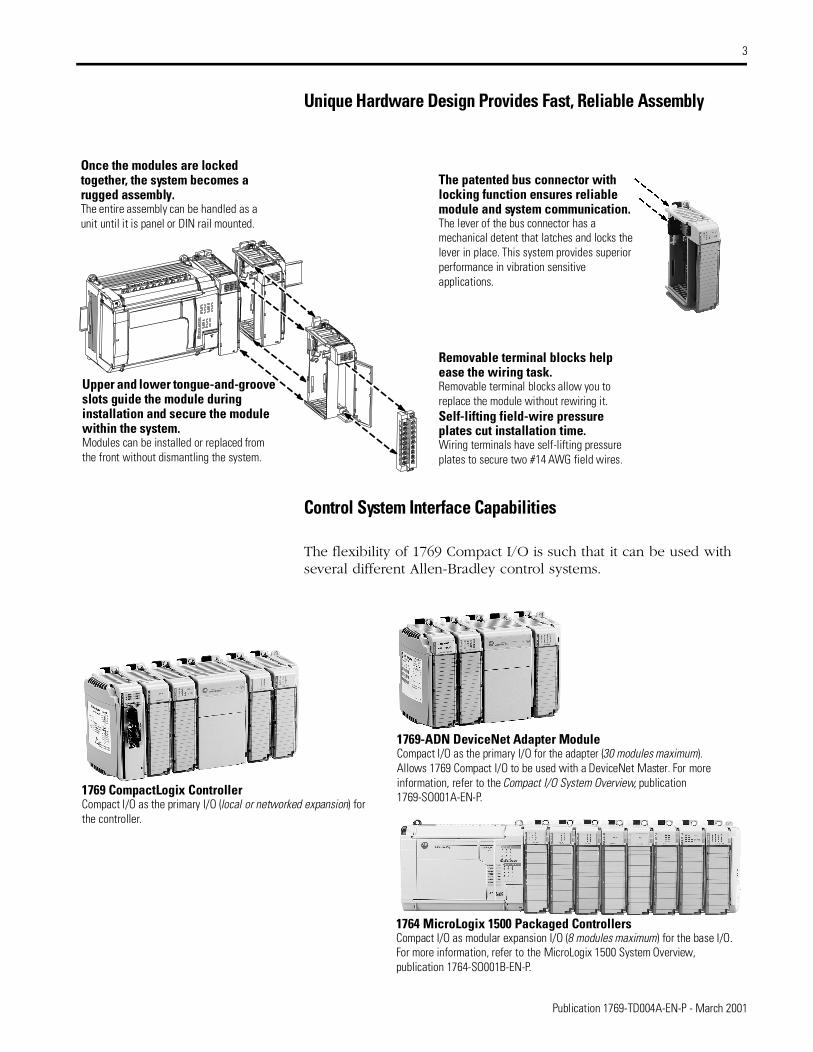
Unique Hardware Design Provides Fast, Reliable Assembly
Control System Interface Capabilities
The flexibility of 1769 Compact I/O is such that it can be used with several different Allen-Bradley control systems.
Upper and lower tongue-and-groove slots guide the module during installation and secure the module within the system. Modules can be installed or replaced from the front without dismantling the system.
Once the modules are locked together, the system becomes a rugged assembly. The entire assembly can be handled as a unit until it is panel or DIN rail mounted.
Removable terminal blocks help ease the wiring task. Removable terminal blocks allow you to replace the module without rewiring it.Self-lifting field-wire pressure plates cut installation time. Wiring terminals have self-lifting pressure plates to secure two #14 AWG field wires.
The patented bus connector with locking function ensures reliable module and system communication. The lever of the bus connector has a mechanical detent that latches and locks the lever in place. This system provides superior performance in vibration sensitive applications.
1764 MicroLogix 1500 Packaged ControllersCompact I/O as modular expansion I/O (8 modules maximum) for the base I/O. For more information, refer to the MicroLogix 1500 System Overview, publication 1764-SO001B-EN-P.
1769-ADN DeviceNet Adapter ModuleCompact I/O as the primary I/O for the adapter (30 modules maximum). Allows 1769 Compact I/O to be used with a DeviceNet Master. For more information, refer to the Compact I/O System Overview, publication 1769-SO001A-EN-P.1769 CompactLogix Controller
Compact I/O as the primary I/O (local or networked expansion) for the controller.
Publication 1769-TD004A-EN-P - March 2001
4 Features and Benefits Common to Analog, Thermocouple and RTD Modules
Features and Benefits Common to Analog, Thermocouple and RTD Modules
All of the modules listed in this publication share the following common features:
Individually configurable channels. Allows the module to be used with a variety of sensors.
Ability to individually enable and disable channels. Disabling unused channels improves module performance.
On-board scaling. Eliminates the need to scale the data in the controller. Controller processing time and power are preserved for more important tasks, such as I/O control, communications, or other user-driven functions.
Selectable input filters. Allows you to select from several different filter frequencies for each channel that best meet the performance needs of your application based on environmental limitations. Lower filter settings provide greater noise rejection and resolution. Higher filter settings provide faster performance. Note: The analog modules provide four input filter selections; RTD and thermocouple modules provide six.
On-line configuration. Modules can be configured in the RUN mode using the programming software or the control program. Allows you to change configuration while the system is operating. For example, the input filter for a particular channel could be changed, or a channel could be disabled based on a batch condition. To use this feature, be sure that the controller or 1769 bus master allows you to do this.
Autocalibration of inputs. The input modules perform autocalibration when a channel is initially enabled. In addition, if a channel is configured differently than the previously scanned channel, an autocalibration cycle is run as part of the reconfiguration process. You can also program the module to perform a periodic calibration cycle.
Over and under-range detection and indication. Eliminates the need to test values in the control program, saving valuable processing power of the controller. In addition, since alarms are handled by the module, the response is faster and only a single bit needs to be monitored to determine if an error condition has occurred.
Selectable response to broken input sensor. This feature provides feedback to the controller that a field device is not connected or operating properly. Allows you to specify corrective action based on the bit or channel condition.
Publication 1769-TD004A-EN-P - March 2001
1769 Analog I/O Modules 5
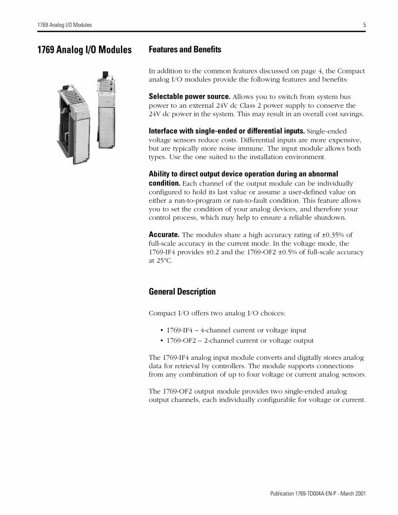
1769 Analog I/O Modules Features and Benefits
In addition to the common features discussed on page 4, the Compact analog I/O modules provide the following features and benefits:
Selectable power source. Allows you to switch from system bus power to an external 24V dc Class 2 power supply to conserve the 24V dc power in the system. This may result in an overall cost savings.
Interface with single-ended or differential inputs. Single-ended voltage sensors reduce costs. Differential inputs are more expensive, but are typically more noise immune. The input module allows both types. Use the one suited to the installation environment.
Ability to direct output device operation during an abnormal condition. Each channel of the output module can be individually configured to hold its last value or assume a user-defined value on either a run-to-program or run-to-fault condition. This feature allows you to set the condition of your analog devices, and therefore your control process, which may help to ensure a reliable shutdown.
Accurate. The modules share a high accuracy rating of ±0.35% of full-scale accuracy in the current mode. In the voltage mode, the 1769-IF4 provides ±0.2 and the 1769-OF2 ±0.5% of full-scale accuracy at 25°C.
General Description
Compact I/O offers two analog I/O choices:
• 1769-IF4 – 4-channel current or voltage input
• 1769-OF2 – 2-channel current or voltage output
The 1769-IF4 analog input module converts and digitally stores analog data for retrieval by controllers. The module supports connections from any combination of up to four voltage or current analog sensors.
The 1769-OF2 output module provides two single-ended analog output channels, each individually configurable for voltage or current.
Publication 1769-TD004A-EN-P - March 2001
6 1769 Analog I/O Modules
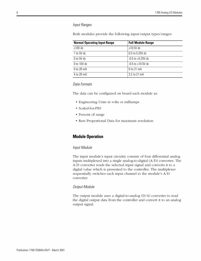
Input Ranges
Both modules provide the following input/output types/ranges:
Data Formats
The data can be configured on board each module as:
• Engineering Units in volts or milliamps
• Scaled-for-PID
• Percent of range
• Raw/Proportional Data for maximum resolution
Module Operation
Input Module
The input module’s input circuitry consists of four differential analog inputs multiplexed into a single analog-to-digital (A/D) converter. The A/D converter reads the selected input signal and converts it to a digital value which is presented to the controller. The multiplexer sequentially switches each input channel to the module’s A/D converter.
Output Module
The output module uses a digital-to-analog (D/A) converter to read the digital output data from the controller and convert it to an analog output signal.
Normal Operating Input Range Full Module Range
±10V dc ±10.5V dc
1 to 5V dc 0.5 to 5.25V dc
0 to 5V dc -0.5 to +5.25V dc
0 to 10V dc -0.5 to +10.5V dc
0 to 20 mA 0 to 21 mA
4 to 20 mA 3.2 to 21 mA
Publication 1769-TD004A-EN-P - March 2001
1769 Analog I/O Modules 7
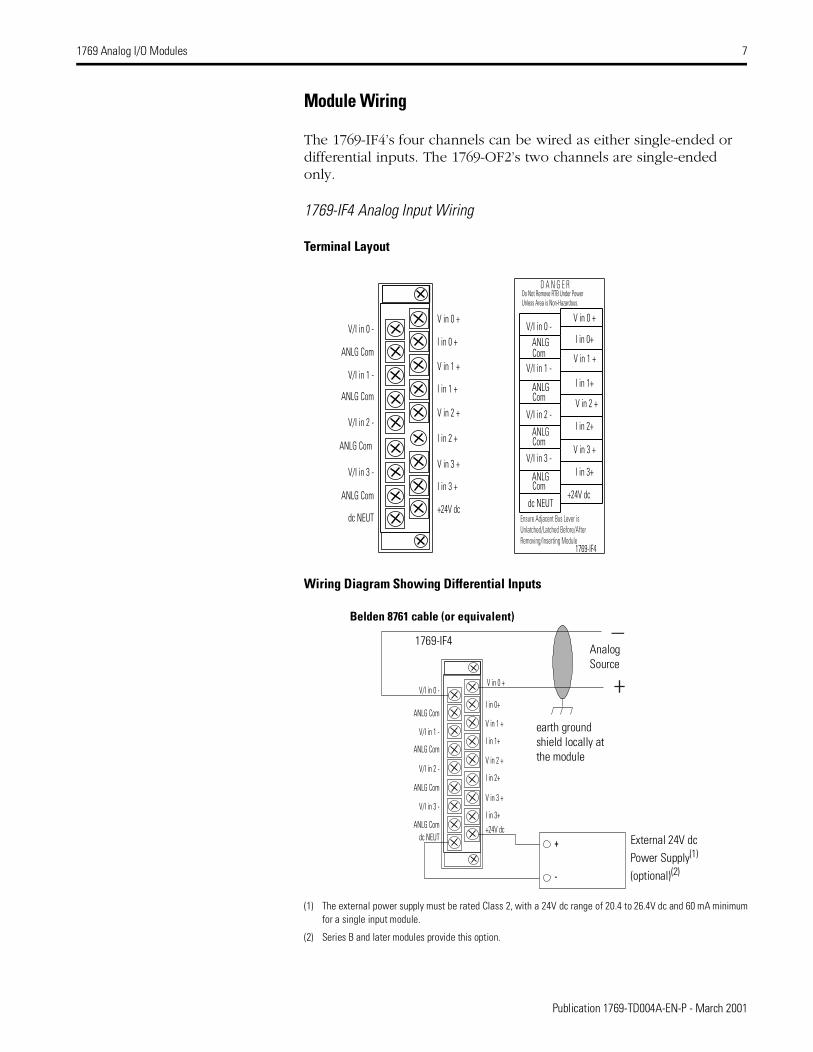
Module Wiring
The 1769-IF4’s four channels can be wired as either single-ended or differential inputs. The 1769-OF2’s two channels are single-ended only.
1769-IF4 Analog Input Wiring
Terminal Layout
Wiring Diagram Showing Differential Inputs
(1) The external power supply must be rated Class 2, with a 24V dc range of 20.4 to 26.4V dc and 60 mA minimum for a single input module.
(2) Series B and later modules provide this option.
V in 0 +V/I in 0 -
I in 0 +ANLG Com
V in 1 +V/I in 1 -
I in 1 +ANLG Com
V in 2 +V/I in 2 -
I in 2 +ANLG Com
V in 3 +V/I in 3 -
I in 3 +ANLG Com
dc NEUT+24V dc
1769-IF4
I in 0+
V in 3 +
+24V dc
V in 1 +
I in 1+
V in 2 +
I in 2+
I in 3+
V in 0 +
ANLGCom
V/I in 3 -
dc NEUT
V/I in 1 -
ANLGCom
V/I in 2 -
ANLGCom
ANLGCom
V/I in 0 -
Ensure Adjacent Bus Lever is Unlatched/Latched Before/After Removing/Inserting Module
D A N G E RDo Not Remove RTB Under Power Unless Area is Non-Hazardous.
+
–
V in 0 +V/I in 0 -
I in 0+ANLG Com
V in 1 +V/I in 1 -
I in 1+ANLG Com
V in 2 +V/I in 2 -
I in 2+ANLG Com
V in 3 +V/I in 3 -
I in 3+ANLG Com
dc NEUT+24V dc
+
-
earth ground shield locally at the module
Analog Source
Belden 8761 cable (or equivalent)
1769-IF4
External 24V dcPower Supply(1)
(optional)(2)
Publication 1769-TD004A-EN-P - March 2001
8 1769 Analog I/O Modules
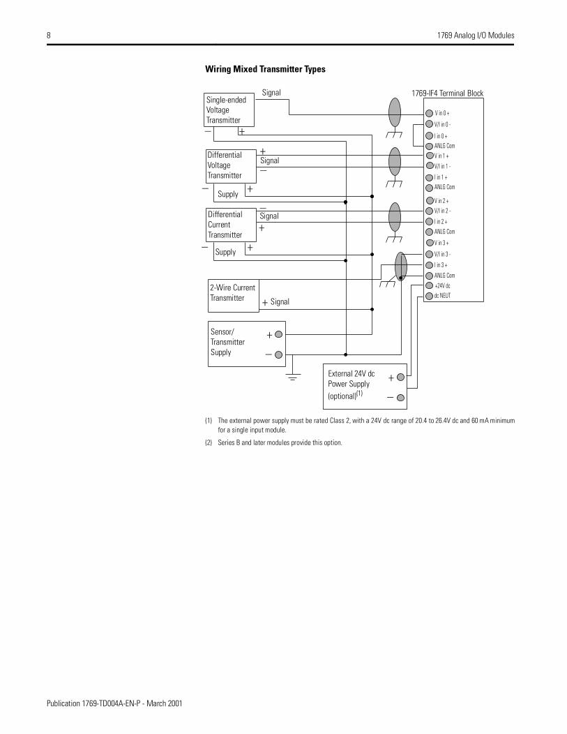
Wiring Mixed Transmitter Types
(1) The external power supply must be rated Class 2, with a 24V dc range of 20.4 to 26.4V dc and 60 mA minimum for a single input module.
(2) Series B and later modules provide this option.
+
V in 0 +
V/I in 0 -
I in 0 +ANLG ComV in 1 +
V/I in 1 -
I in 1 +ANLG Com
V in 2 +V/I in 2 -
I in 2 +ANLG Com
V in 3 +
V/I in 3 -
I in 3 +
ANLG Com+24V dcdc NEUT
+
+
+
+
+
+
–
–
–
–
–
–
+
–
Single-ended Voltage Transmitter
Differential Voltage Transmitter
Differential Current Transmitter
2-Wire Current Transmitter
Signal
Signal
Signal
Signal
Supply
Supply
Sensor/Transmitter Supply
1769-IF4 Terminal Block
External 24V dc Power Supply(optional)(1)
Publication 1769-TD004A-EN-P - March 2001
1769 Analog I/O Modules 9
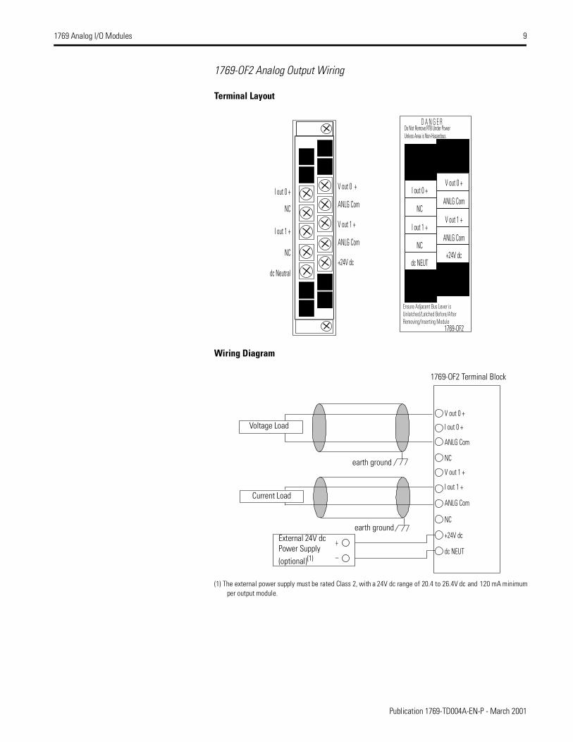
1769-OF2 Analog Output Wiring
Terminal Layout
Wiring Diagram
(1) The external power supply must be rated Class 2, with a 24V dc range of 20.4 to 26.4V dc and 120 mA minimum per output module.
V out 0 +I out 0 +
ANLG ComNC
V out 1 +I out 1 +
ANLG Com
dc Neutral
NC+24V dc
1769-OF2
I in 0
NC
I in 3
V in 0 +
ANLGCom 0
NC
ANLG Com
+24V dc
V out 1 +
ANLG Com
V out 0 +
NC
dc NEUT
I out 1 +
NC
I out 0 +
ANLGCom 3
V in 0 -
D A N G E R
Ensure Adjacent Bus Lever is Unlatched/Latched Before/After Removing/Inserting Module
Do Not Remove RTB Under PowerUnless Area is Non-Hazardous.
V out 0 +
I out 0 +
ANLG Com
NC
V out 1 +
I out 1 +
ANLG Com
NC
+24V dc
dc NEUT+
–
Voltage Load
Current Load
earth ground
1769-OF2 Terminal Block
earth groundExternal 24V dc Power Supply(optional)(1)
Publication 1769-TD004A-EN-P - March 2001
10 1769 Analog I/O Modules
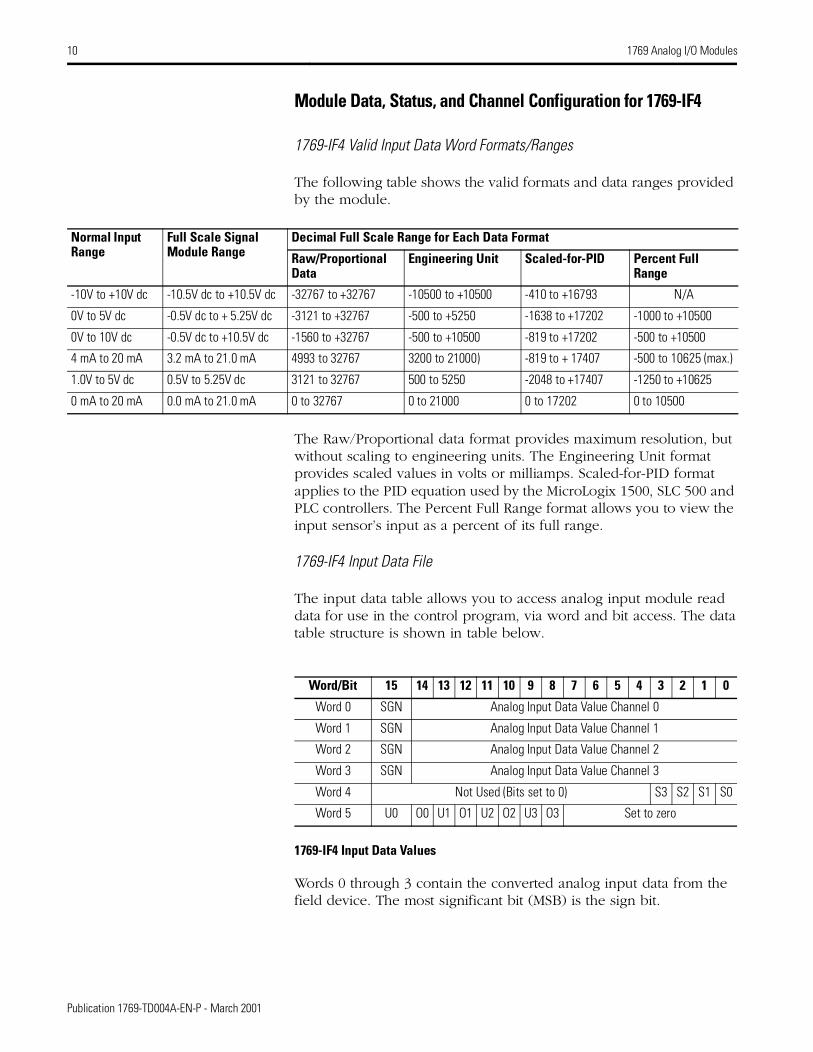
Module Data, Status, and Channel Configuration for 1769-IF4
1769-IF4 Valid Input Data Word Formats/Ranges
The following table shows the valid formats and data ranges provided by the module.
The Raw/Proportional data format provides maximum resolution, but without scaling to engineering units. The Engineering Unit format provides scaled values in volts or milliamps. Scaled-for-PID format applies to the PID equation used by the MicroLogix 1500, SLC 500 and PLC controllers. The Percent Full Range format allows you to view the input sensor’s input as a percent of its full range.
1769-IF4 Input Data File
The input data table allows you to access analog input module read data for use in the control program, via word and bit access. The data table structure is shown in table below.
1769-IF4 Input Data Values
Words 0 through 3 contain the converted analog input data from the field device. The most significant bit (MSB) is the sign bit.
Normal Input Range
Full Scale Signal Module Range
Decimal Full Scale Range for Each Data Format
Raw/Proportional Data
Engineering Unit Scaled-for-PID Percent Full Range
-10V to +10V dc -10.5V dc to +10.5V dc -32767 to +32767 -10500 to +10500 -410 to +16793 N/A
0V to 5V dc -0.5V dc to + 5.25V dc -3121 to +32767 -500 to +5250 -1638 to +17202 -1000 to +10500
0V to 10V dc -0.5V dc to +10.5V dc -1560 to +32767 -500 to +10500 -819 to +17202 -500 to +10500
4 mA to 20 mA 3.2 mA to 21.0 mA 4993 to 32767 3200 to 21000) -819 to + 17407 -500 to 10625 (max.)
1.0V to 5V dc 0.5V to 5.25V dc 3121 to 32767 500 to 5250 -2048 to +17407 -1250 to +10625
0 mA to 20 mA 0.0 mA to 21.0 mA 0 to 32767 0 to 21000 0 to 17202 0 to 10500
Word/Bit 15 14 13 12 11 10 9 8 7 6 5 4 3 2 1 0
Word 0 SGN Analog Input Data Value Channel 0
Word 1 SGN Analog Input Data Value Channel 1
Word 2 SGN Analog Input Data Value Channel 2
Word 3 SGN Analog Input Data Value Channel 3
Word 4 Not Used (Bits set to 0) S3 S2 S1 S0
Word 5 U0 O0 U1 O1 U2 O2 U3 O3 Set to zero
Publication 1769-TD004A-EN-P - March 2001
1769 Analog I/O Modules 11
General Status Bits (S0 through S3)
Word 4, bits 0 through 3 contain the general operational status bits for input channels 0 through 3. If set (1), these bits indicate an error associated with that channel.
Over-Range Flag Bits (O0 through O3)
Over-range bits for channels 3 through 0 are contained in word 5, bits 8, 10, 12, and 14. They apply to all input types. When set (1), this bit indicates input signals beyond the normal operating range.
Under-Range Flag Bits (U0 through U3)
Under-range bits for channels 3 through 0 are contained in word 5, bits 9, 11, 13, and 15. They apply to all input types. When set (1), this bit indicates input signals below the normal operating range. It may also indicate an open circuit condition, when the module is configured for the 4 to 20 mA range.
1769-IF4 Channel Configuration
The configuration file is typically modified using the programming software configuration screen. The configuration file can also be modified through the control program, if supported by the controller.
Publication 1769-TD004A-EN-P - March 2001
12 1769 Analog I/O Modules
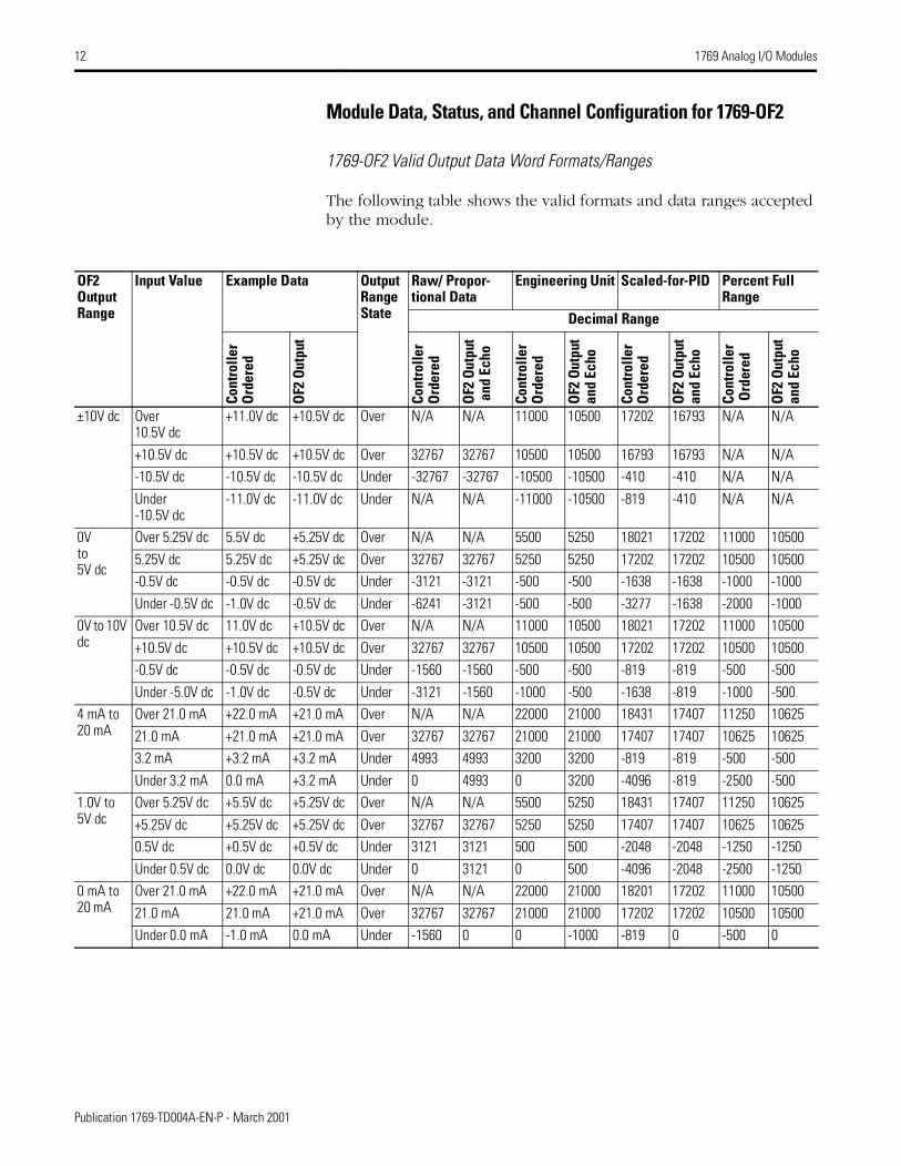
Module Data, Status, and Channel Configuration for 1769-OF2
1769-OF2 Valid Output Data Word Formats/Ranges
The following table shows the valid formats and data ranges accepted by the module.
OF2 Output Range
Input Value Example Data Output Range State
Raw/ Propor-tional Data
Engineering Unit Scaled-for-PID Percent Full Range
Decimal Range
Cont
rolle
r O
rder
ed
OF2
Out
put
Cont
rolle
r O
rder
ed
OF2
Out
put
and
Ech
o
Cont
rolle
r O
rder
ed
OF2
Out
put
and
Echo
Cont
rolle
r O
rder
ed
OF2
Out
put
and
Echo
Cont
rolle
r O
rder
ed
OF2
Out
put
and
Echo
±10V dc Over 10.5V dc
+11.0V dc +10.5V dc Over N/A N/A 11000 10500 17202 16793 N/A N/A
+10.5V dc +10.5V dc +10.5V dc Over 32767 32767 10500 10500 16793 16793 N/A N/A-10.5V dc -10.5V dc -10.5V dc Under -32767 -32767 -10500 -10500 -410 -410 N/A N/AUnder -10.5V dc
-11.0V dc -11.0V dc Under N/A N/A -11000 -10500 -819 -410 N/A N/A
0V to5V dc
Over 5.25V dc 5.5V dc +5.25V dc Over N/A N/A 5500 5250 18021 17202 11000 105005.25V dc 5.25V dc +5.25V dc Over 32767 32767 5250 5250 17202 17202 10500 10500-0.5V dc -0.5V dc -0.5V dc Under -3121 -3121 -500 -500 -1638 -1638 -1000 -1000Under -0.5V dc -1.0V dc -0.5V dc Under -6241 -3121 -500 -500 -3277 -1638 -2000 -1000
0V to 10V dc
Over 10.5V dc 11.0V dc +10.5V dc Over N/A N/A 11000 10500 18021 17202 11000 10500+10.5V dc +10.5V dc +10.5V dc Over 32767 32767 10500 10500 17202 17202 10500 10500-0.5V dc -0.5V dc -0.5V dc Under -1560 -1560 -500 -500 -819 -819 -500 -500Under -5.0V dc -1.0V dc -0.5V dc Under -3121 -1560 -1000 -500 -1638 -819 -1000 -500
4 mA to 20 mA
Over 21.0 mA +22.0 mA +21.0 mA Over N/A N/A 22000 21000 18431 17407 11250 1062521.0 mA +21.0 mA +21.0 mA Over 32767 32767 21000 21000 17407 17407 10625 106253.2 mA +3.2 mA +3.2 mA Under 4993 4993 3200 3200 -819 -819 -500 -500Under 3.2 mA 0.0 mA +3.2 mA Under 0 4993 0 3200 -4096 -819 -2500 -500
1.0V to5V dc
Over 5.25V dc +5.5V dc +5.25V dc Over N/A N/A 5500 5250 18431 17407 11250 10625+5.25V dc +5.25V dc +5.25V dc Over 32767 32767 5250 5250 17407 17407 10625 106250.5V dc +0.5V dc +0.5V dc Under 3121 3121 500 500 -2048 -2048 -1250 -1250Under 0.5V dc 0.0V dc 0.0V dc Under 0 3121 0 500 -4096 -2048 -2500 -1250
0 mA to 20 mA
Over 21.0 mA +22.0 mA +21.0 mA Over N/A N/A 22000 21000 18201 17202 11000 1050021.0 mA 21.0 mA +21.0 mA Over 32767 32767 21000 21000 17202 17202 10500 10500Under 0.0 mA -1.0 mA 0.0 mA Under -1560 0 0 -1000 -819 0 -500 0
Publication 1769-TD004A-EN-P - March 2001
1769 Analog I/O Modules 13
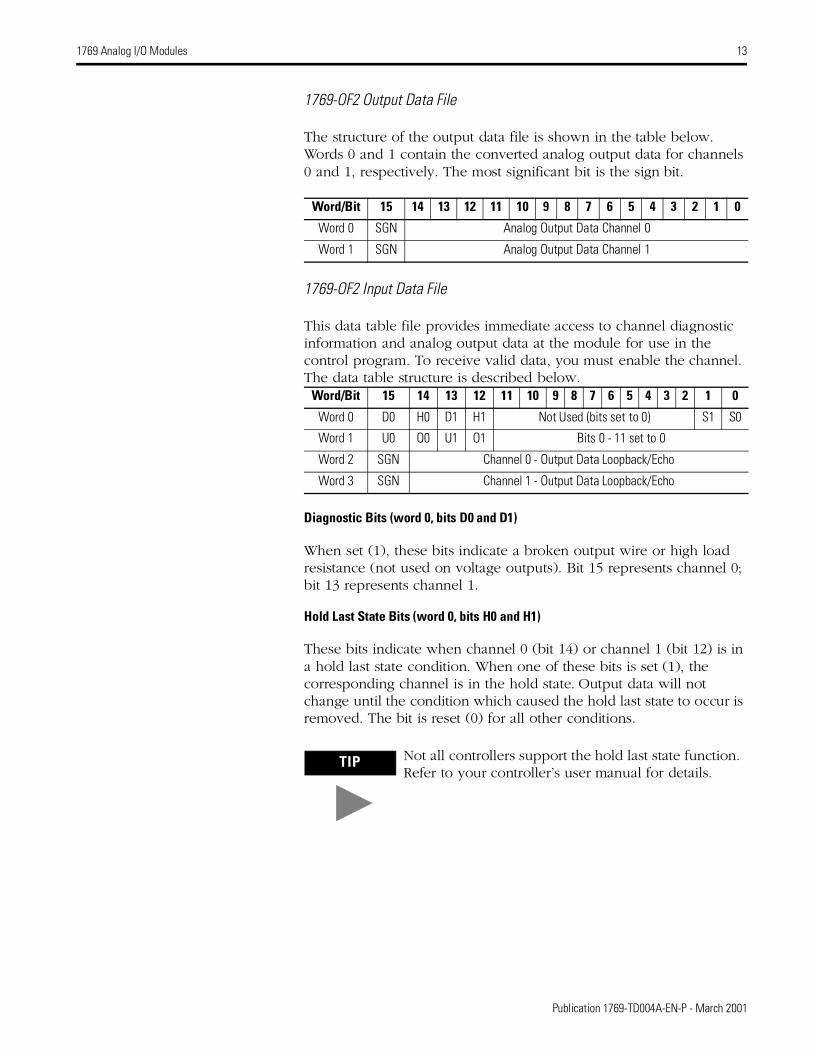
1769-OF2 Output Data File
The structure of the output data file is shown in the table below. Words 0 and 1 contain the converted analog output data for channels 0 and 1, respectively. The most significant bit is the sign bit.
1769-OF2 Input Data File
This data table file provides immediate access to channel diagnostic information and analog output data at the module for use in the control program. To receive valid data, you must enable the channel. The data table structure is described below.
Diagnostic Bits (word 0, bits D0 and D1)
When set (1), these bits indicate a broken output wire or high load resistance (not used on voltage outputs). Bit 15 represents channel 0; bit 13 represents channel 1.
Hold Last State Bits (word 0, bits H0 and H1)
These bits indicate when channel 0 (bit 14) or channel 1 (bit 12) is in a hold last state condition. When one of these bits is set (1), the corresponding channel is in the hold state. Output data will not change until the condition which caused the hold last state to occur is removed. The bit is reset (0) for all other conditions.
Word/Bit 15 14 13 12 11 10 9 8 7 6 5 4 3 2 1 0
Word 0 SGN Analog Output Data Channel 0
Word 1 SGN Analog Output Data Channel 1
Word/Bit 15 14 13 12 11 10 9 8 7 6 5 4 3 2 1 0
Word 0 D0 H0 D1 H1 Not Used (bits set to 0) S1 S0
Word 1 U0 O0 U1 O1 Bits 0 - 11 set to 0
Word 2 SGN Channel 0 - Output Data Loopback/Echo
Word 3 SGN Channel 1 - Output Data Loopback/Echo
TIP Not all controllers support the hold last state function. Refer to your controller’s user manual for details.
Publication 1769-TD004A-EN-P - March 2001
14 1769 Analog I/O Modules
Over-Range Flag Bits (word 1, bits O0 and O1)
Over-range bits for channels 0 and 1 are contained in word 1, bits 14 and 12. When set, the over-range bit indicates that the controller is attempting to drive the analog output above its normal operating range. However, the module continues to convert analog output data to a maximum full range value. The bit is automatically reset (0) by the module when the over-range condition is cleared.
Under-Range Flag Bits (word 1, bits U0 and U1)
Under-range bits for channels 0 and 1 are contained in word 1, bits 15 and 13. When set (1), the under-range bit indicates that the controller is attempting to drive the analog output below its normal operating range. However, the module continues to convert analog output data to a minimum full range value. The bit is automatically reset (0) by the module when the under-range condition is cleared.
General Status Bits (word 0, bits S0 and S1)
Word 0, bits 0 and 1 contain the general status information for output channels 0 and 1. If set (1), these bits indicate an error associated with that channel.
Output Data Loopback/Echo (words 2 and 3)
Words 2 and 3 provide output loopback/data echo through the input array for channels 0 and 1, respectively. The value of the data echo is the analog value currently being converted on-board the module by the D/A converter. This ensures that the logic-directed state of the output is true. Otherwise, the state of the output could vary depending on controller mode.
Under normal operating conditions, the data echo value is the same value that is being sent from the controller to the output module. Under abnormal conditions, the values may differ. For example:
1. During run mode, the control program could direct the module to a value over or under the defined full range. In that case, the module raises the over- or under-range flag and continues to convert and data echo up to the defined full range. However, upon reaching either the maximum upper or lower full range value, the module stops converting and echoes back that maximum upper or lower full range value, not the value being sent from the controller.
2. During program or fault mode with Hold Last State or User-Defined Value selected, the module echoes the hold last value or alternate value as selected by the user.
Publication 1769-TD004A-EN-P - March 2001
1769 Analog I/O Modules 15
Channel Configuration
The configuration file is typically modified using the programming software configuration screen. The configuration file can also be modified through the control program, if supported by the controller.
Module Diagnostics
The 1769-IF4 and 1769-OF2 modules contain diagnostic features that can help you identify the source of problems that may occur during power-up or during normal channel operation.
Module-level operation includes functions such as powerup, configuration, and communication with a bus master, such as a MicroLogix 1500 controller. Channel-level operation describes channel-related functions, such as data conversion and over- and under-range detection.
Internal diagnostics are performed at both levels of operation and any error conditions detected are immediately indicated by the module status LED. Both module hardware and channel configuration error conditions are reported to the controller.
PowerUp Diagnostics
At module powerup, a series of internal diagnostic tests is performed. If any test fails, the status LED remains off, a modules error results and is reported to the controller.
Channel Diagnostics
When a channel is enabled, a diagnostic check is performed to verify that the channel has been properly configured. In addition, the channel is tested for out-of-range and open-circuit faults on every scan for configuration errors, over- and under-range, open-circuit (4 to 20 mA input only), and output wire broken/high load resistance (output only) conditions.
A failure of any channel diagnostic test causes the faulted channel LED to blink. Channel faults are self-clearing, and the channel LED will stop blinking and resume steady illumination when the fault conditions are removed.
Publication 1769-TD004A-EN-P - March 2001
16 1769 Analog I/O Modules
Analog Modules Specifications
1769-IF4 (Series B) Analog Input Module Specifications
Specification 1769-IF4
Analog Normal Operating Ranges Voltage: ±10V dc, 0 to 10V dc, 0 to 5V dc, 1 to 5V dcCurrent: 0 to 20 mA, 4 to 20 mA
Number of Inputs 4 differential or single-ended
Bus Current Draw (max.) 120 mA at 5V dc, 60 mA at 24V dc(3) (2.52W)
Resolution (max.) 14 bits (unipolar) 14 bits plus sign (bipolar), with 50 or 60 Hz filter selected
Normal Mode Rejection Ratio -50 dB at 50 and 60 Hz with 50 or 60 Hz filter selected
Input Impedance Voltage Terminal: 220K Ω, Current Terminal: 250 Ω
Overall Accuracy(1) Voltage Terminal: ±0.2% full scale at 25°CCurrent Terminal: ±0.35% full scale at 25°C
Non-linearity (in percent full scale) ±0.03%
Repeatability(2) ±0.03%
Module Error over Full Temperature Range (0 to +60°C [+32°F to +140°F])
Voltage: ±0.3%Current: ±0.5%
Input Channel Configuration Via configuration software screen or the user program.
Field Input Calibration Not required
Channel Diagnostics Over- or under-range by bit reporting
Power Supply Distance Rating 8 (The maximum distance an I/O module may be located from the power supply is 8 modules.)
Input Group to Bus Isolation 500V ac or 710V dc for 1 minute (qualification test)30V ac/30V dc working voltage (IEC Class 2 reinforced insulation)
(1) Includes offset, gain, non-linearity and repeatability error terms.
(2) Repeatability is the ability of the input module to register the same reading in successive measurements for the same input signal.
(3) The Series B and later analog input module has the ability to connect an external 24V dc, Class 2 power supply (20.4 to 24.6V dc, 60 mA per module) as an option to using the 24V dc of the 1769 system power supply (e.g. 1769-PA2).
Publication 1769-TD004A-EN-P - March 2001
1769 Analog I/O Modules 17
1769-OF2 (Series B) Analog Output Module Specifications
Specification 1769-OF2
Analog Ranges Voltage: ±10V dc, 0 to 10V dc, 0 to 5V dc, 1 to 5V dcCurrent: 0 to 20 mA, 4 to 20 mA
Number of Outputs 2 single-ended
Bus Current Draw (max.) 120 mA at 5V dc, 120 mA at 24V dc(4) (2.63W)
Resolution (max.) 14-bit unipolar, 14-bit plus-sign bipolar with 50/60 Hz filter selected
Conversion Rate (all channels) max. 2.5 ms
Step Response to 63%(1) 2.9 ms
Current Load on Voltage Output 10 mA max.
Resistive Load on Current Output 0 to 500 Ω (includes wire resistance)
Load Range on Voltage Output > 1k Ω at 10V dc
Max. Inductive Load(Current Outputs)
0.1 mH
Max. Capacitive Load(Voltage Outputs)
1 µF
Field Calibration None required
Overall Accuracy(2) Voltage Terminal: ±0.5% full scale at 25°C, Current Terminal: ±0.35% full scale at 25°C
Non-linearity (in percent full scale) ±0.05%
Repeatability(3) (in percent full scale) ±0.05%
Output Error Over Full Temperature Range(0 to 60°C [32 to +140°F])
Voltage: ±0.8%Current: ±0.55%
Open and Short-Circuit Protection Yes
Output Overvoltage Protection Yes
Channel Diagnostics Over-or-under range by bit reportingoutput wire broken or load resistance high by bit reporting (current mode only)
Power Supply Distance Rating 8 (The maximum distance an I/O module may be located from the power supply is 8 modules.)
Output Group to Backplane Isolation 500V ac or 710V dc for 1 minute (qualification test)30V ac/30V dc working voltage (IEC Class 2 reinforced insulation)
(1) Step response is the period of time between when the D/A converter was instructed to go from minimum to full range until the device is at 63% of full range.
(2) Includes offset, gain, non-linearity and repeatability error terms.
(3) Repeatability is the ability of the output module to reproduce output readings when the same controller value is applied to it consecutively, under the same conditions and in the same direction.
(4) The Series B and later analog output module has the ability to connect an external 24V dc, Class 2 power supply (20.4 to 24.6V dc, 60 mA per module) as an option to using the 24V dc of the 1769 system power supply (e.g. 1769-PA2).
Publication 1769-TD004A-EN-P - March 2001
18 1769-IT6 Thermocouple Input Module
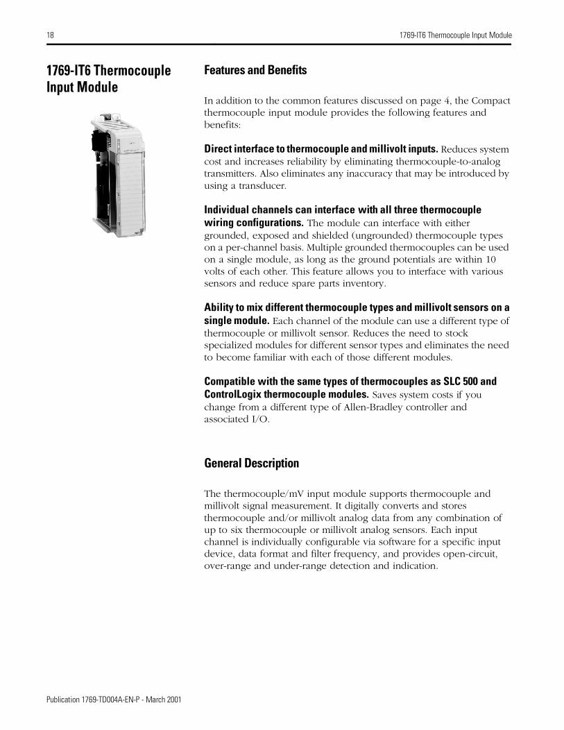
1769-IT6 Thermocouple Input Module
Features and Benefits
In addition to the common features discussed on page 4, the Compact thermocouple input module provides the following features and benefits:
Direct interface to thermocouple and millivolt inputs. Reduces system cost and increases reliability by eliminating thermocouple-to-analog transmitters. Also eliminates any inaccuracy that may be introduced by using a transducer.
Individual channels can interface with all three thermocouple wiring configurations. The module can interface with either grounded, exposed and shielded (ungrounded) thermocouple types on a per-channel basis. Multiple grounded thermocouples can be used on a single module, as long as the ground potentials are within 10 volts of each other. This feature allows you to interface with various sensors and reduce spare parts inventory.
Ability to mix different thermocouple types and millivolt sensors on a single module. Each channel of the module can use a different type of thermocouple or millivolt sensor. Reduces the need to stock specialized modules for different sensor types and eliminates the need to become familiar with each of those different modules.
Compatible with the same types of thermocouples as SLC 500 and ControlLogix thermocouple modules. Saves system costs if you change from a different type of Allen-Bradley controller and associated I/O.
General Description
The thermocouple/mV input module supports thermocouple and millivolt signal measurement. It digitally converts and stores thermocouple and/or millivolt analog data from any combination of up to six thermocouple or millivolt analog sensors. Each input channel is individually configurable via software for a specific input device, data format and filter frequency, and provides open-circuit, over-range and under-range detection and indication.
Publication 1769-TD004A-EN-P - March 2001
1769-IT6 Thermocouple Input Module 19
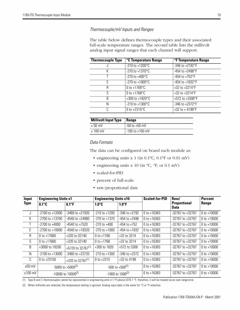
Thermocouple/mV Inputs and Ranges
The table below defines thermocouple types and their associated full-scale temperature ranges. The second table lists the millivolt analog input signal ranges that each channel will support.
Data Formats
The data can be configured on board each module as:
• engineering units x 1 (in 0.1°C, 0.1°F or 0.01 mV)
• engineering units x 10 (in °C, °F, or 0.1 mV)
• scaled-for-PID
• percent of full-scale
• raw/proportional data
Thermocouple Type °C Temperature Range °F Temperature RangeJ -210 to +1200°C -346 to +2192°FK -270 to +1370°C -454 to +2498°FT -270 to +400°C -454 to +752°FE -270 to +1000°C -454 to +1832°FR 0 to +1768°C +32 to +3214°FS 0 to +1768°C +32 to +3214°FB +300 to +1820°C +572 to +3308°FN -210 to +1300°C -346 to +2372°FC 0 to +2315°C +32 to + 4199°F
Millivolt Input Type Range± 50 mV -50 to +50 mV± 100 mV -100 to +100 mV
Input Type
Engineering Units x1 Engineering Units x10 Scaled-for-PID Raw/Proportional Data
Percent Range0.1°C 0.1°F 1.0°C 1.0°F
J -2100 to +12000 -3460 to +21920 -210 to +1200 -346 to +2192 0 to +16383 -32767 to +32767 0 to +10000K -2700 to +13700 -4540 to +24980 -270 to +1370 -454 to +2498 0 to +16383 -32767 to +32767 0 to +10000T -2700 to +4000 -4540 to +7520 -270 to +400 -454 to +752 0 to +16383 -32767 to +32767 0 to +10000E -2700 to +10000 -4540 to +18320 -270 to +1000 -454 to +1832 0 to +16383 -32767 to +32767 0 to +10000R 0 to +17680 +320 to 32140 0 to +1768 +32 to 3214 0 to +16383 -32767 to +32767 0 to +10000S 0 to +17680 +320 to 32140 0 to +1768 +32 to 3214 0 to +16383 -32767 to +32767 0 to +10000B +3000 to 18200 +5720 to 32767(1) +300 to 1820 +572 to 3308 0 to +16383 -32767 to +32767 0 to +10000
N -2100 to +13000 -3460 to +23720 -210 to +1300 -346 to +2372 0 to +16383 -32767 to +32767 0 to +10000C 0 to +23150 +320 to 32767(1) 0 to +2315 +32 to 4199 0 to +16383 -32767 to +32767 0 to +10000
±50 mV -5000 to +5000(2) -500 to +500(2) 0 to +16383 -32767 to +32767 0 to +10000
±100 mV -10000 to 10000(2) -1000 to 1000(2) 0 to +16383 -32767 to +32767 0 to +10000
(1) Type B and C thermocouples cannot be represented in engineering units x1 (°F) above 3276.7 °F; therefore, it will be treated as an over-range error.
(2) When millivolts are selected, the temperature setting is ignored. Analog input date is the same for °C or °F selection.
Publication 1769-TD004A-EN-P - March 2001
20 1769-IT6 Thermocouple Input Module
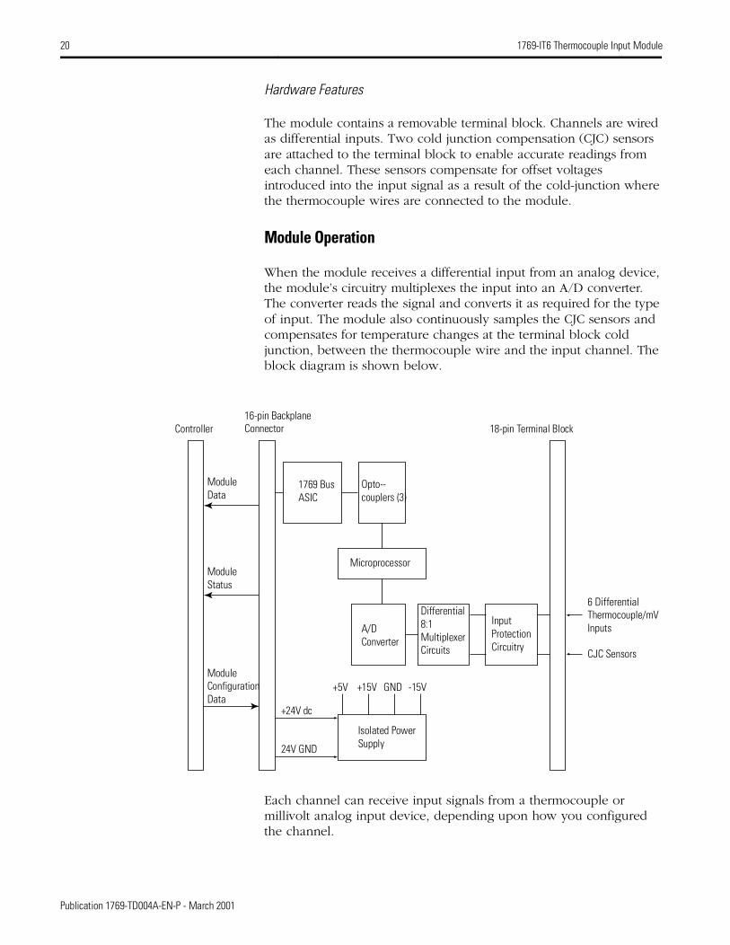
Hardware Features
The module contains a removable terminal block. Channels are wired as differential inputs. Two cold junction compensation (CJC) sensors are attached to the terminal block to enable accurate readings from each channel. These sensors compensate for offset voltages introduced into the input signal as a result of the cold-junction where the thermocouple wires are connected to the module.
Module Operation
When the module receives a differential input from an analog device, the module’s circuitry multiplexes the input into an A/D converter. The converter reads the signal and converts it as required for the type of input. The module also continuously samples the CJC sensors and compensates for temperature changes at the terminal block cold junction, between the thermocouple wire and the input channel. The block diagram is shown below.
Each channel can receive input signals from a thermocouple or millivolt analog input device, depending upon how you configured the channel.
18-pin Terminal Block16-pin Backplane Connector
1769 Bus ASIC
Opto--couplers (3)
A/DConverter
Differential8:1 MultiplexerCircuits
InputProtectionCircuitry
Microprocessor
6 DifferentialThermocouple/mVInputs
CJC Sensors
+24V dc
24V GND
Isolated Power Supply
+5V +15V GND -15V
Module Data
Module Status
Module Configuration Data
Controller
Publication 1769-TD004A-EN-P - March 2001
1769-IT6 Thermocouple Input Module 21
When configured for thermocouple input types, the module converts the analog input voltages into cold-junction compensated and linearized digital temperature readings. The module uses the National Institute of Standards and Technology (NIST) ITS-90 standard for linearization for all thermocouple types (J, K, T, E, R, S, B, N, C).
When configured for millivolt inputs, the module converts the analog values directly into digital counts.
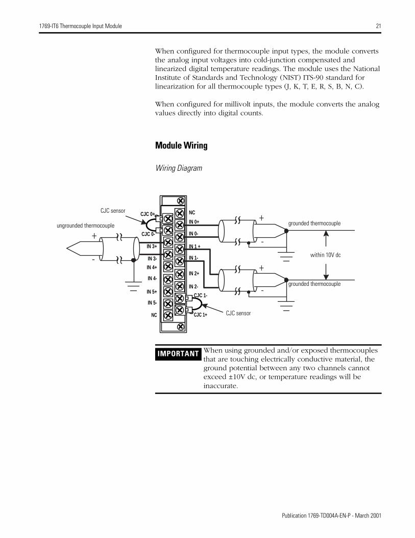
Module Wiring
Wiring Diagram
NC
IN 0+
IN 0-
IN 3+ IN 1 +
IN 3- IN 1-
IN 4+IN 2+
IN 4-IN 2-
IN 5+
IN 5-
NC
+
-+
-
+
-
CJC 0+
CJC 0-
CJC 1-
CJC 1+
within 10V dc
grounded thermocouple
grounded thermocouple
ungrounded thermocouple
CJC sensor
CJC sensor
IMPORTANT When using grounded and/or exposed thermocouples that are touching electrically conductive material, the ground potential between any two channels cannot exceed ±10V dc, or temperature readings will be inaccurate.
Publication 1769-TD004A-EN-P - March 2001
22 1769-IT6 Thermocouple Input Module
Module Data, Status, and Channel Configuration
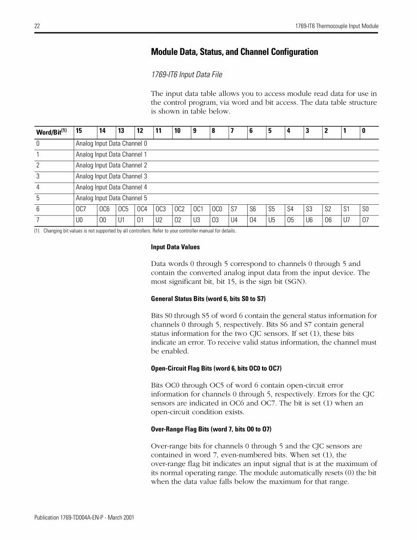
1769-IT6 Input Data File
The input data table allows you to access module read data for use in the control program, via word and bit access. The data table structure is shown in table below.
Input Data Values
Data words 0 through 5 correspond to channels 0 through 5 and contain the converted analog input data from the input device. The most significant bit, bit 15, is the sign bit (SGN).
General Status Bits (word 6, bits S0 to S7)
Bits S0 through S5 of word 6 contain the general status information for channels 0 through 5, respectively. Bits S6 and S7 contain general status information for the two CJC sensors. If set (1), these bits indicate an error. To receive valid status information, the channel must be enabled.
Open-Circuit Flag Bits (word 6, bits OC0 to OC7)
Bits OC0 through OC5 of word 6 contain open-circuit error information for channels 0 through 5, respectively. Errors for the CJC sensors are indicated in OC6 and OC7. The bit is set (1) when an open-circuit condition exists.
Over-Range Flag Bits (word 7, bits O0 to O7)
Over-range bits for channels 0 through 5 and the CJC sensors are contained in word 7, even-numbered bits. When set (1), the over-range flag bit indicates an input signal that is at the maximum of its normal operating range. The module automatically resets (0) the bit when the data value falls below the maximum for that range.
Word/Bit(1) 15 14 13 12 11 10 9 8 7 6 5 4 3 2 1 0
0 Analog Input Data Channel 0
1 Analog Input Data Channel 1
2 Analog Input Data Channel 2
3 Analog Input Data Channel 3
4 Analog Input Data Channel 4
5 Analog Input Data Channel 5
6 OC7 OC6 OC5 OC4 OC3 OC2 OC1 OC0 S7 S6 S5 S4 S3 S2 S1 S0
7 U0 O0 U1 O1 U2 O2 U3 O3 U4 O4 U5 O5 U6 O6 U7 O7(1) Changing bit values is not supported by all controllers. Refer to your controller manual for details.
Publication 1769-TD004A-EN-P - March 2001
1769-IT6 Thermocouple Input Module 23
Under-Range Flag Bits (word 7, bits U0 to U7)
Under-range bits for channels 0 through 5 and the CJC sensors are contained in word 7, odd-numbered bits. When set (1), the under-range flag bit indicates an input signal that is at the minimum of its normal operating range. The module automatically resets (0) the bit when the under-range condition is cleared.
General Diagnostic Features
The module contains a diagnostic LED that helps you identify the source of problems that may occur during power-up or during normal channel operation. The LED indicates both status and power.
Power-up Diagnostics
At module power-up, a series of internal diagnostic tests are performed. If these diagnostic tests are not successfully completed, the module status LED remains off and a module error is reported to the controller.
Channel Diagnostics
When an input channel is enabled, the module performs a diagnostic check to see that the channel has been properly configured. In addition, the channel is tested on every scan for configuration errors, over-range and under-range, and open-circuit conditions.
Publication 1769-TD004A-EN-P - March 2001
24 1769-IT6 Thermocouple Input Module
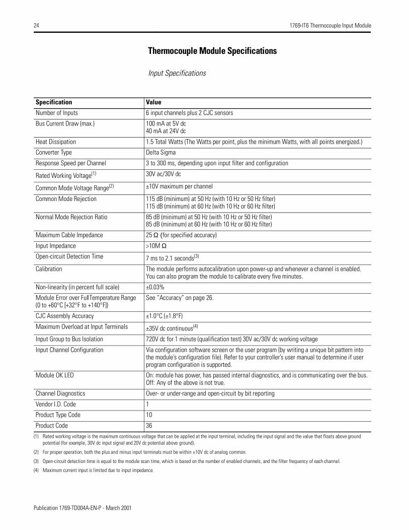
Thermocouple Module Specifications
Input Specifications
Specification Value
Number of Inputs 6 input channels plus 2 CJC sensors
Bus Current Draw (max.) 100 mA at 5V dc40 mA at 24V dc
Heat Dissipation 1.5 Total Watts (The Watts per point, plus the minimum Watts, with all points energized.)
Converter Type Delta Sigma
Response Speed per Channel 3 to 300 ms, depending upon input filter and configuration
Rated Working Voltage(1) 30V ac/30V dc
Common Mode Voltage Range(2) ±10V maximum per channel
Common Mode Rejection 115 dB (minimum) at 50 Hz (with 10 Hz or 50 Hz filter)115 dB (minimum) at 60 Hz (with 10 Hz or 60 Hz filter)
Normal Mode Rejection Ratio 85 dB (minimum) at 50 Hz (with 10 Hz or 50 Hz filter)85 dB (minimum) at 60 Hz (with 10 Hz or 60 Hz filter)
Maximum Cable Impedance 25 Ω (for specified accuracy)
Input Impedance >10M ΩOpen-circuit Detection Time 7 ms to 2.1 seconds(3)
Calibration The module performs autocalibration upon power-up and whenever a channel is enabled. You can also program the module to calibrate every five minutes.
Non-linearity (in percent full scale) ±0.03%
Module Error over Full Temperature Range (0 to +60°C [+32°F to +140°F])
See “Accuracy” on page 26.
CJC Assembly Accuracy ±1.0°C (±1.8°F)
Maximum Overload at Input Terminals ±35V dc continuous(4)
Input Group to Bus Isolation 720V dc for 1 minute (qualification test) 30V ac/30V dc working voltage
Input Channel Configuration Via configuration software screen or the user program (by writing a unique bit pattern into the module’s configuration file). Refer to your controller’s user manual to determine if user program configuration is supported.
Module OK LED On: module has power, has passed internal diagnostics, and is communicating over the bus.Off: Any of the above is not true.
Channel Diagnostics Over- or under-range and open-circuit by bit reporting
Vendor I.D. Code 1
Product Type Code 10
Product Code 36
(1) Rated working voltage is the maximum continuous voltage that can be applied at the input terminal, including the input signal and the value that floats above ground potential (for example, 30V dc input signal and 20V dc potential above ground).
(2) For proper operation, both the plus and minus input terminals must be within ±10V dc of analog common.
(3) Open-circuit detection time is equal to the module scan time, which is based on the number of enabled channels, and the filter frequency of each channel.
(4) Maximum current input is limited due to input impedance.
Publication 1769-TD004A-EN-P - March 2001
1769-IT6 Thermocouple Input Module 25
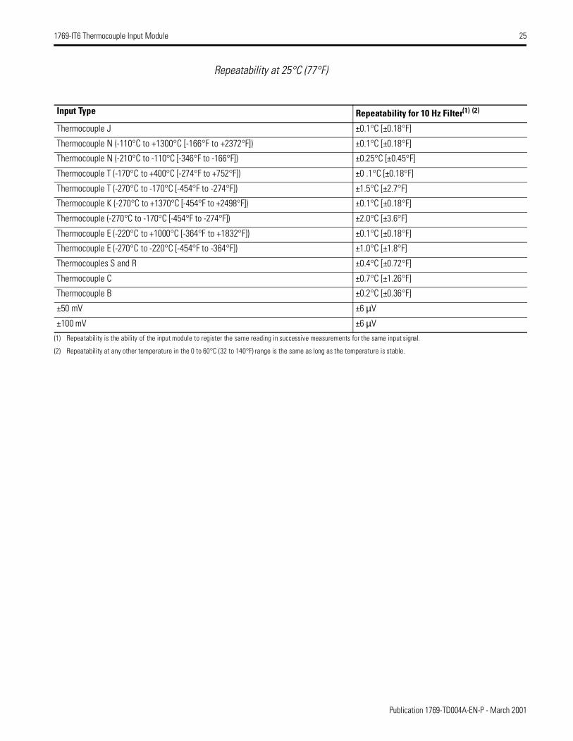
Repeatability at 25°C (77°F)
Input Type Repeatability for 10 Hz Filter(1) (2)
Thermocouple J ±0.1°C [±0.18°F]
Thermocouple N (-110°C to +1300°C [-166°F to +2372°F]) ±0.1°C [±0.18°F]
Thermocouple N (-210°C to -110°C [-346°F to -166°F]) ±0.25°C [±0.45°F]
Thermocouple T (-170°C to +400°C [-274°F to +752°F]) ±0 .1°C [±0.18°F]
Thermocouple T (-270°C to -170°C [-454°F to -274°F]) ±1.5°C [±2.7°F]
Thermocouple K (-270°C to +1370°C [-454°F to +2498°F]) ±0.1°C [±0.18°F]
Thermocouple (-270°C to -170°C [-454°F to -274°F]) ±2.0°C [±3.6°F]
Thermocouple E (-220°C to +1000°C [-364°F to +1832°F]) ±0.1°C [±0.18°F]
Thermocouple E (-270°C to -220°C [-454°F to -364°F]) ±1.0°C [±1.8°F]
Thermocouples S and R ±0.4°C [±0.72°F]
Thermocouple C ±0.7°C [±1.26°F]
Thermocouple B ±0.2°C [±0.36°F]
±50 mV ±6 µV
±100 mV ±6 µV(1) Repeatability is the ability of the input module to register the same reading in successive measurements for the same input signal.
(2) Repeatability at any other temperature in the 0 to 60°C (32 to 140°F) range is the same as long as the temperature is stable.
Publication 1769-TD004A-EN-P - March 2001
26 1769-IT6 Thermocouple Input Module
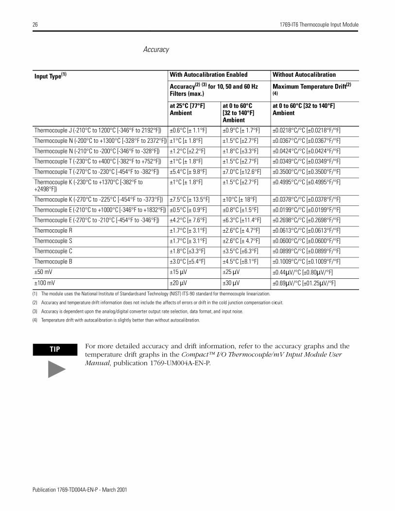
Accuracy
Input Type(1) With Autocalibration Enabled Without Autocalibration
Accuracy(2) (3) for 10, 50 and 60 Hz Filters (max.)
Maximum Temperature Drift(2) (4)
at 25°C [77°F]Ambient
at 0 to 60°C [32 to 140°F] Ambient
at 0 to 60°C [32 to 140°F]Ambient
Thermocouple J (-210°C to 1200°C [-346°F to 2192°F]) ±0.6°C [± 1.1°F] ±0.9°C [± 1.7°F] ±0.0218°C/°C [±0.0218°F/°F]
Thermocouple N (-200°C to +1300°C [-328°F to 2372°F]) ±1°C [± 1.8°F] ±1.5°C [±2.7°F] ±0.0367°C/°C [±0.0367°F/°F]
Thermocouple N (-210°C to -200°C [-346°F to -328°F]) ±1.2°C [±2.2°F] ±1.8°C [±3.3°F] ±0.0424°C/°C [±0.0424°F/°F]
Thermocouple T (-230°C to +400°C [-382°F to +752°F]) ±1°C [± 1.8°F] ±1.5°C [±2.7°F] ±0.0349°C/°C [±0.0349°F/°F]
Thermocouple T (-270°C to -230°C [-454°F to -382°F]) ±5.4°C [± 9.8°F] ±7.0°C [±12.6°F] ±0.3500°C/°C [±0.3500°F/°F]
Thermocouple K (-230°C to +1370°C [-382°F to +2498°F])
±1°C [± 1.8°F] ±1.5°C [±2.7°F] ±0.4995°C/°C [±0.4995°F/°F]
Thermocouple K (-270°C to -225°C [-454°F to -373°F]) ±7.5°C [± 13.5°F] ±10°C [± 18°F] ±0.0378°C/°C [±0.0378°F/°F]
Thermocouple E (-210°C to +1000°C [-346°F to +1832°F]) ±0.5°C [± 0.9°F] ±0.8°C [±1.5°F] ±0.0199°C/°C [±0.0199°F/°F]
Thermocouple E (-270°C to -210°C [-454°F to -346°F]) ±4.2°C [± 7.6°F] ±6.3°C [±11.4°F] ±0.2698°C/°C [±0.2698°F/°F]
Thermocouple R ±1.7°C [± 3.1°F] ±2.6°C [± 4.7°F] ±0.0613°C/°C [±0.0613°F/°F]
Thermocouple S ±1.7°C [± 3.1°F] ±2.6°C [± 4.7°F] ±0.0600°C/°C [±0.0600°F/°F]
Thermocouple C ±1.8°C [±3.3°F] ±3.5°C [±6.3°F] ±0.0899°C/°C [±0.0899°F/°F]
Thermocouple B ±3.0°C [±5.4°F] ±4.5°C [±8.1°F] ±0.1009°C/°C [±0.1009°F/°F]
±50 mV ±15 µV ±25 µV ±0.44µV/°C [±0.80µV/°F]
±100 mV ±20 µV ±30 µV ±0.69µV/°C [±01.25µV/°F]
(1) The module uses the National Institute of Standards and Technology (NIST) ITS-90 standard for thermocouple linearization.
(2) Accuracy and temperature drift information does not include the affects of errors or drift in the cold junction compensation circuit.
(3) Accuracy is dependent upon the analog/digital converter output rate selection, data format, and input noise.
(4) Temperature drift with autocalibration is slightly better than without autocalibration.
TIP For more detailed accuracy and drift information, refer to the accuracy graphs and the temperature drift graphs in the Compact™ I/O Thermocouple/mV Input Module User Manual, publication 1769-UM004A-EN-P.
Publication 1769-TD004A-EN-P - March 2001
1769-IR6 RTD/Resistance Input Module 27
1769-IR6 RTD/Resistance Input Module
Features and Benefits
In addition to the common features discussed on page 4, the Compact RTD input module provides the following features and benefits:
Direct interface to Resistance Temperature Detectors (RTDs) and resistance inputs. Reduces system cost and increases reliability by eliminating expensive RTD-to-analog transmitters. Also eliminates any inaccuracy that may be introduced by using a transducer.
Individual channels can interface with all three RTD wiring configurations. The module can interface with 2, 3, or 4-wire RTDS on a per-channel basis. The different wiring configurations allow you to select the RTD that best suits your cost and accuracy targets. This feature allows you to interface with various sensors and reduce spare parts inventory.
Ability to mix different RTD types and resistance sensors on a single module. Each channel of the module can use a different type of RTD or resistance sensor. Reduces the need to stock specialized modules for different sensor types and eliminates the need to become familiar with each of those different modules.
Compatible with the same RTD types as SLC 500 and ControlLogix thermocouple modules. Saves system costs if you change from a different type of Allen-Bradley controller and associated I/O.
Two RTD excitation current selections, configurable per channel. Applying the appropriate current reduces RTD self-heating and improves accuracy.
Publication 1769-TD004A-EN-P - March 2001
28 1769-IR6 RTD/Resistance Input Module
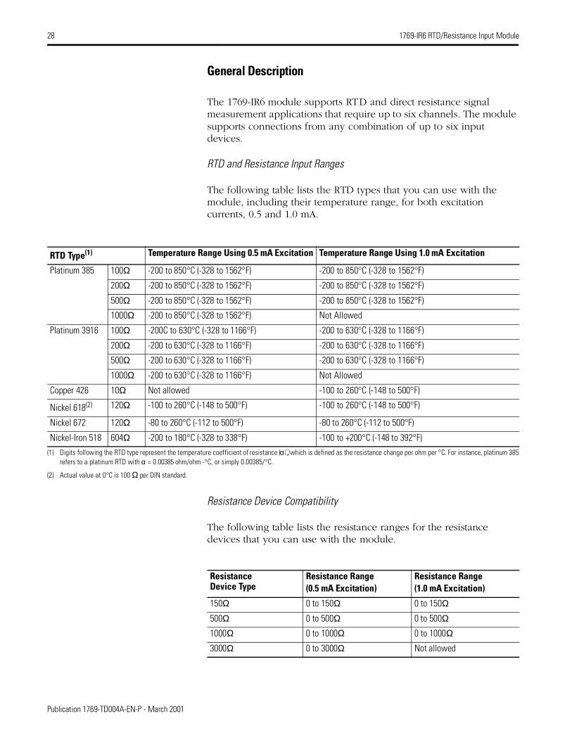
General Description
The 1769-IR6 module supports RTD and direct resistance signal measurement applications that require up to six channels. The module supports connections from any combination of up to six input devices.
RTD and Resistance Input Ranges
The following table lists the RTD types that you can use with the module, including their temperature range, for both excitation currents, 0.5 and 1.0 mA.
Resistance Device Compatibility
The following table lists the resistance ranges for the resistance devices that you can use with the module.
RTD Type(1) Temperature Range Using 0.5 mA Excitation Temperature Range Using 1.0 mA Excitation
Platinum 385 100Ω -200 to 850°C (-328 to 1562°F) -200 to 850°C (-328 to 1562°F)
200Ω -200 to 850°C (-328 to 1562°F) -200 to 850°C (-328 to 1562°F)
500Ω -200 to 850°C (-328 to 1562°F) -200 to 850°C (-328 to 1562°F)
1000Ω -200 to 850°C (-328 to 1562°F) Not Allowed
Platinum 3916 100Ω -200C to 630°C (-328 to 1166°F) -200 to 630°C (-328 to 1166°F)
200Ω -200 to 630°C (-328 to 1166°F) -200 to 630°C (-328 to 1166°F)
500Ω -200 to 630°C (-328 to 1166°F) -200 to 630°C (-328 to 1166°F)
1000Ω -200 to 630°C (-328 to 1166°F) Not Allowed
Copper 426 10Ω Not allowed -100 to 260°C (-148 to 500°F)
Nickel 618(2) 120Ω -100 to 260°C (-148 to 500°F) -100 to 260°C (-148 to 500°F)
Nickel 672 120Ω -80 to 260°C (-112 to 500°F) -80 to 260°C (-112 to 500°F)
Nickel-Iron 518 604Ω -200 to 180°C (-328 to 338°F) -100 to +200°C (-148 to 392°F)(1) Digits following the RTD type represent the temperature coefficient of resistance (α), which is defined as the resistance change per ohm per °C. For instance, platinum 385
refers to a platinum RTD with α = 0.00385 ohm/ohm -°C, or simply 0.00385/°C.
(2) Actual value at 0°C is 100 Ω per DIN standard.
Resistance Device Type
Resistance Range (0.5 mA Excitation)
Resistance Range(1.0 mA Excitation)
150Ω 0 to 150Ω 0 to 150Ω
500Ω 0 to 500Ω 0 to 500Ω1000Ω 0 to 1000Ω 0 to 1000Ω
3000Ω 0 to 3000Ω Not allowed
Publication 1769-TD004A-EN-P - March 2001
1769-IR6 RTD/Resistance Input Module 29
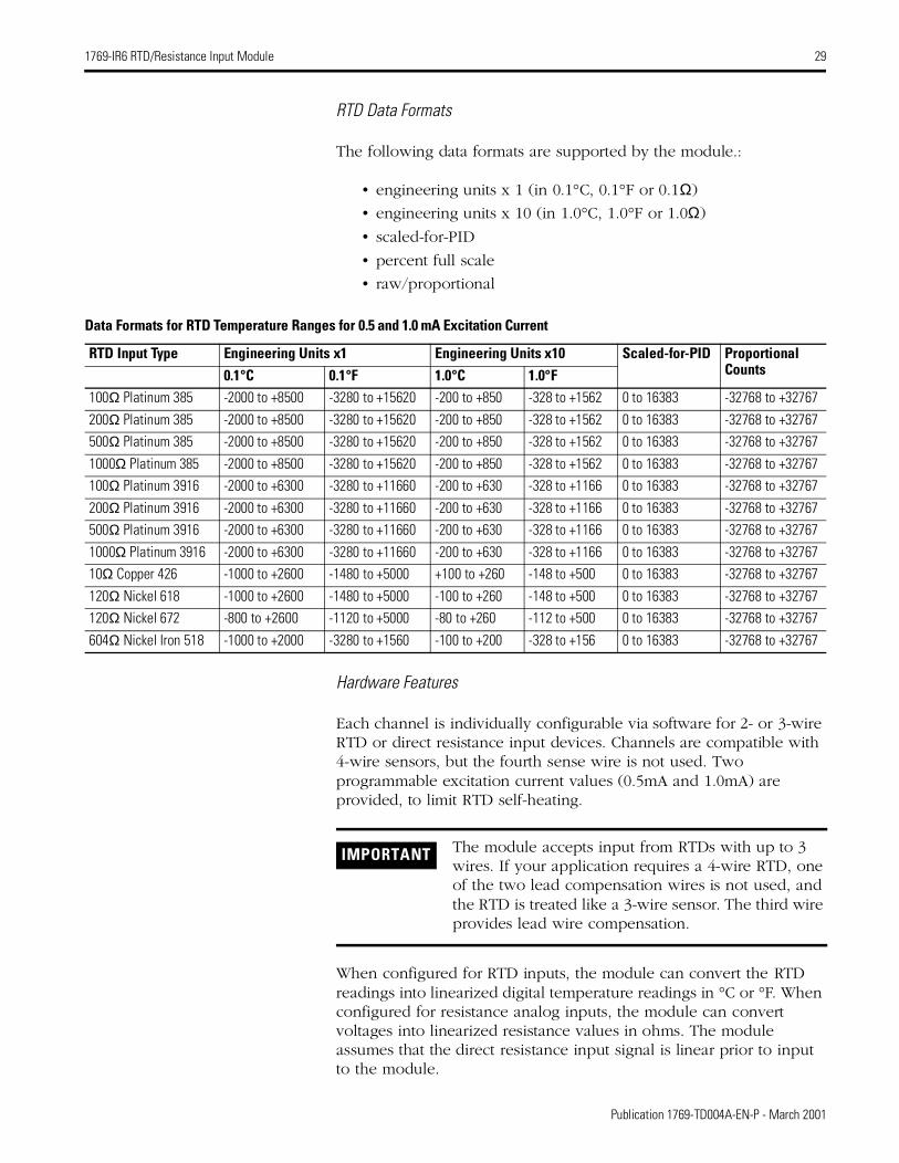
RTD Data Formats
The following data formats are supported by the module.:
• engineering units x 1 (in 0.1°C, 0.1°F or 0.1Ω)
• engineering units x 10 (in 1.0°C, 1.0°F or 1.0Ω)
• scaled-for-PID
• percent full scale
• raw/proportional
Hardware Features
Each channel is individually configurable via software for 2- or 3-wire RTD or direct resistance input devices. Channels are compatible with 4-wire sensors, but the fourth sense wire is not used. Two programmable excitation current values (0.5mA and 1.0mA) are provided, to limit RTD self-heating.
When configured for RTD inputs, the module can convert the RTD readings into linearized digital temperature readings in °C or °F. When configured for resistance analog inputs, the module can convert voltages into linearized resistance values in ohms. The module assumes that the direct resistance input signal is linear prior to input to the module.
Data Formats for RTD Temperature Ranges for 0.5 and 1.0 mA Excitation Current
RTD Input Type Engineering Units x1 Engineering Units x10 Scaled-for-PID Proportional Counts0.1°C 0.1°F 1.0°C 1.0°F
100Ω Platinum 385 -2000 to +8500 -3280 to +15620 -200 to +850 -328 to +1562 0 to 16383 -32768 to +32767200Ω Platinum 385 -2000 to +8500 -3280 to +15620 -200 to +850 -328 to +1562 0 to 16383 -32768 to +32767500Ω Platinum 385 -2000 to +8500 -3280 to +15620 -200 to +850 -328 to +1562 0 to 16383 -32768 to +327671000Ω Platinum 385 -2000 to +8500 -3280 to +15620 -200 to +850 -328 to +1562 0 to 16383 -32768 to +32767100Ω Platinum 3916 -2000 to +6300 -3280 to +11660 -200 to +630 -328 to +1166 0 to 16383 -32768 to +32767200Ω Platinum 3916 -2000 to +6300 -3280 to +11660 -200 to +630 -328 to +1166 0 to 16383 -32768 to +32767500Ω Platinum 3916 -2000 to +6300 -3280 to +11660 -200 to +630 -328 to +1166 0 to 16383 -32768 to +327671000Ω Platinum 3916 -2000 to +6300 -3280 to +11660 -200 to +630 -328 to +1166 0 to 16383 -32768 to +3276710Ω Copper 426 -1000 to +2600 -1480 to +5000 +100 to +260 -148 to +500 0 to 16383 -32768 to +32767120Ω Nickel 618 -1000 to +2600 -1480 to +5000 -100 to +260 -148 to +500 0 to 16383 -32768 to +32767120Ω Nickel 672 -800 to +2600 -1120 to +5000 -80 to +260 -112 to +500 0 to 16383 -32768 to +32767604Ω Nickel Iron 518 -1000 to +2000 -3280 to +1560 -100 to +200 -328 to +156 0 to 16383 -32768 to +32767
IMPORTANT The module accepts input from RTDs with up to 3 wires. If your application requires a 4-wire RTD, one of the two lead compensation wires is not used, and the RTD is treated like a 3-wire sensor. The third wire provides lead wire compensation.
Publication 1769-TD004A-EN-P - March 2001
30 1769-IR6 RTD/Resistance Input Module
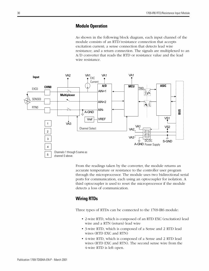
Module Operation
As shown in the following block diagram, each input channel of the module consists of an RTD/resistance connection that accepts excitation current; a sense connection that detects lead wire resistance; and a return connection. The signals are multiplexed to an A/D converter that reads the RTD or resistance value and the lead wire resistance.
From the readings taken by the converter, the module returns an accurate temperature or resistance to the controller user program through the microprocessor. The module uses two bidirectional serial ports for communication, each using an optocoupler for isolation. A third optocoupler is used to reset the microprocessor if the module detects a loss of communication.
Wiring RTDs
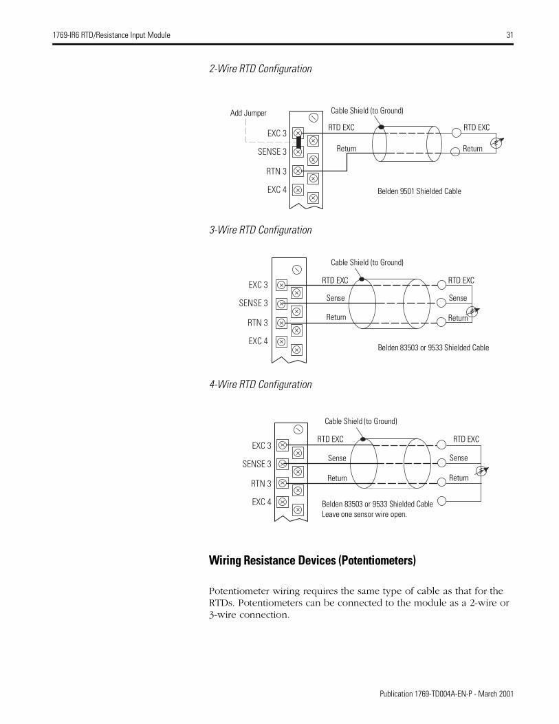
Three types of RTDs can be connected to the 1769-IR6 module:
• 2-wire RTD, which is composed of an RTD EXC (excitation) lead wire and a RTN (return) lead wire
• 3-wire RTD, which is composed of a Sense and 2 RTD lead wires (RTD EXC and RTN)
• 4-wire RTD, which is composed of a Sense and 2 RTD lead wires (RTD EXC and RTN). The second sense wire from the 4-wire RTD is left open.
VA2
A-GND
VA1 VA1
AIN+1
AIN+2
AIN-
VREFVref
VA3
VA1
TXD
VA1
VA2
VA3
A-GND
VS2
VS1
S-GND
1
2
3
4
5
Input
EXC0
SENSE0
RTN0
CHN0
Multiplexer
EXC Current
A/D MCU ASIC
BUS
Channel Select
DC/DCPower Supply
Channels 1 through 5 same as channel 0 above.
Publication 1769-TD004A-EN-P - March 2001
1769-IR6 RTD/Resistance Input Module 31
2-Wire RTD Configuration
3-Wire RTD Configuration
4-Wire RTD Configuration
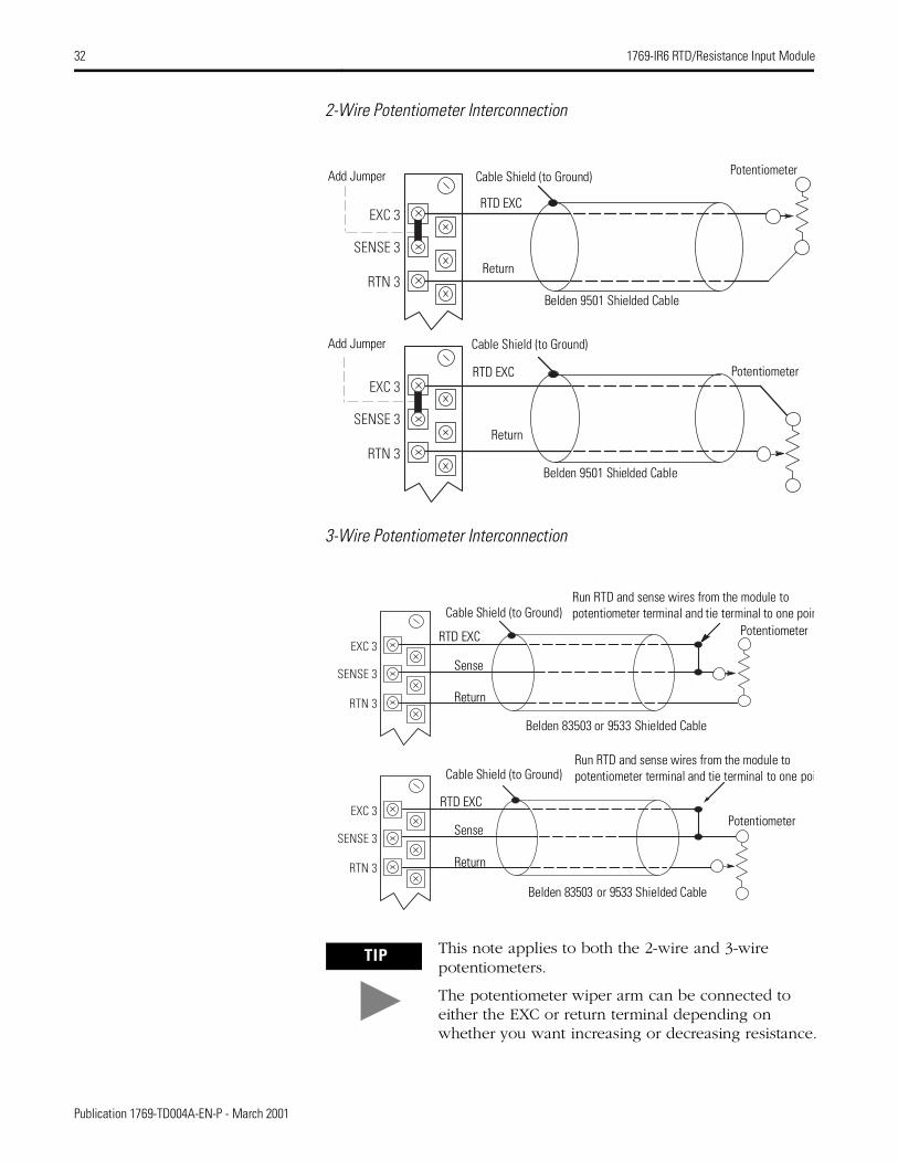
Wiring Resistance Devices (Potentiometers)
Potentiometer wiring requires the same type of cable as that for the RTDs. Potentiometers can be connected to the module as a 2-wire or 3-wire connection.
EXC 3
SENSE 3
RTN 3
EXC 4 Belden 9501 Shielded Cable
Cable Shield (to Ground)
RTD EXC
Return
RTD EXC
Return
Add Jumper
EXC 3
SENSE 3
RTN 3
EXC 4Belden 83503 or 9533 Shielded Cable
Cable Shield (to Ground)
RTD EXC
Sense
RTD EXC
Return
Sense
Return
EXC 3
SENSE 3
RTN 3
EXC 4 Belden 83503 or 9533 Shielded CableLeave one sensor wire open.
Cable Shield (to Ground)
RTD EXC
Return
RTD EXC
Return
Sense Sense
Publication 1769-TD004A-EN-P - March 2001
32 1769-IR6 RTD/Resistance Input Module
2-Wire Potentiometer Interconnection
3-Wire Potentiometer Interconnection
TIP This note applies to both the 2-wire and 3-wire potentiometers.
The potentiometer wiper arm can be connected to either the EXC or return terminal depending on whether you want increasing or decreasing resistance.
EXC 3
SENSE 3
RTN 3
EXC 3
SENSE 3
RTN 3
Cable Shield (to Ground) Potentiometer
RTD EXC
Return
Add Jumper
Cable Shield (to Ground)
PotentiometerRTD EXC
Return
Add Jumper
Belden 9501 Shielded Cable
Belden 9501 Shielded Cable
EXC 3
SENSE 3
RTN 3
EXC 3
SENSE 3
RTN 3
Cable Shield (to Ground)PotentiometerRTD EXC
Return
Sense
Run RTD and sense wires from the module to potentiometer terminal and tie terminal to one poin
Cable Shield (to Ground)
PotentiometerRTD EXC
Return
Sense
Run RTD and sense wires from the module to potentiometer terminal and tie terminal to one poi
Belden 83503 or 9533 Shielded Cable
Belden 83503 or 9533 Shielded Cable
Publication 1769-TD004A-EN-P - March 2001
1769-IR6 RTD/Resistance Input Module 33
1769-IR6 Module Data, Status, and Channel Configuration
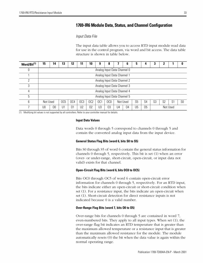
Input Data File
The input data table allows you to access RTD input module read data for use in the control program, via word and bit access. The data table structure is shown in table below.
Input Data Values
Data words 0 through 5 correspond to channels 0 through 5 and contain the converted analog input data from the input device.
General Status Flag Bits (word 6, bits S0 to S5)
Bits S0 through S5 of word 6 contain the general status information for channels 0 through 5, respectively. This bit is set (1) when an error (over- or under-range, short-circuit, open-circuit, or input data not valid) exists for that channel.
Open-Circuit Flag Bits (word 6, bits OC0 to OC5)
Bits OC0 through OC5 of word 6 contain open-circuit error information for channels 0 through 5, respectively. For an RTD input, the bits indicate either an open-circuit or short-circuit condition when set (1). For a resistance input, the bits indicate an open-circuit when set (1). Short-circuit detection for direct resistance inputs is not indicated because 0 is a valid number.
Over-Range Flag Bits (word 7, bits O0 to O5)
Over-range bits for channels 0 through 5 are contained in word 7, even-numbered bits. They apply to all input types. When set (1), the over-range flag bit indicates an RTD temperature that is greater than the maximum allowed temperature or a resistance input that is greater than the maximum allowed resistance for the module. The module automatically resets (0) the bit when the data value is again within the normal operating range.
Word/Bit(1) 15 14 13 12 11 10 9 8 7 6 5 4 3 2 1 0
0 Analog Input Data Channel 0
1 Analog Input Data Channel 1
2 Analog Input Data Channel 2
3 Analog Input Data Channel 3
4 Analog Input Data Channel 4
5 Analog Input Data Channel 5
6 Not Used OC5 OC4 OC3 OC2 OC1 OC0 Not Used S5 S4 S3 S2 S1 S0
7 U0 O0 U1 O1 U2 O2 U3 O3 U4 O4 U5 O5 Not Used(1) Modifying bit values is not supported by all controllers. Refer to your controller manual for details.
Publication 1769-TD004A-EN-P - March 2001
34 1769-IR6 RTD/Resistance Input Module
Under-Range Flag Bits (word 7, bits U0 to U5)
Under-range bits for channels 0 through 5 are contained in word 7, odd-numbered bits. They apply only to RTD input types. When set (1), the under-range flag bit indicates an RTD temperature that is less than the minimum allowed temperature. The module automatically resets (0) the bit when the data value is again within the normal operating range. There is no under-range error for a direct resistance input, because 0 is a valid number.
Channel Configuration
Normal channel configuration is done using programming software. In that case, it is not necessary to know the meaning of the bit location. However, some systems allow configuration to be changed by the control program, but not all controllers support program access to the configuration file. Refer to your controller’s documentation for details.
Module Diagnostics
The module performs diagnostic operations at both the module level and the channel level. Module-level operations include functions such as power-up, configuration, and communication with a 1769 bus master, such as a MicroLogix 1500 controller, 1769-ADN DeviceNet Adapter or CompactLogix controller.
Channel-level operations describe channel related functions, such as data conversion and over- or under-range detection.
Internal diagnostics are performed at both levels of operation. When detected, module error conditions are immediately indicated by the module status LED. Both module hardware and channel configuration error conditions are reported to the controller. Channel over-range or under-range conditions are reported in the module’s input data table. Module hardware errors are typically reported in the controller’s I/O status file. Refer to your controller manual for details.
Power-up Diagnostics
At module power-up, a series of internal diagnostic tests are performed. These diagnostic tests must be successfully completed or the module status LED remains off and a module error results and is reported to the controller.
Channel Diagnostics
When an input channel is enabled, the module performs a diagnostic check to see that the channel has been properly configured. In addition, the channel is tested on every scan for configuration errors, over-range and under-range, and broken input conditions.
Publication 1769-TD004A-EN-P - March 2001
1769-IR6 RTD/Resistance Input Module 35
RTD Module Specifications
Input Specifications
Specification 1769-IR6Bus Current Draw (max.) 100 mA at 5V dc
45 mA at 24V dcHeat Dissipation 1.5 Total Watts (The Watts per point, plus the minimum Watts, with all points enabled.)Converter Type Sigma-DeltaResolution Input filter and configuration dependent.
Common Mode Voltage Range(1) ±10V dc maximum per channel
Common Mode Rejection 110 dB minimum at 50 Hz with the 10 or 50 Hz filter selected110 dB minimum at 60 Hz with the 10 or 60 Hz filter selected
Normal Mode Rejection Ratio 70 dB minimum at 50 Hz with the 10 or 50 Hz filter selected70 dB minimum at 60 Hz with the 10 or 60 Hz filter selected
Non-linearity(in percent full-scale)
±0.05%
Typical Accuracy [Autocalibration Enabled] at 25° C (77°F) Ambient with Module Operating Temperature at 25° C (77°F) (2)
±0.5°C (°F) for Pt 385±0.4°C (°F) for Pt 3916±0.2°C (°F) for Ni±0.3°C (°F) for NiFe±0.6°C (°F) for Cu
±0.15Ω for 150Ω range±0.5Ω for 500Ω range±1.0Ω for 1000Ω range±1.5Ω for 3000Ω range
Typical Accuracy [Autocalibration Enabled] at 0 to 60° C (+32 to +140°F)(2)
±0.9°C (°F) for Pt 385±0.8°C (°F) for Pt 3916±0.4°C (°F) for Ni±0.5°C (°F) for NiFe±1.1°C (°F) for Cu
±0.25Ω for 150Ω range±0.8Ω for 500Ω range±1.5Ω for 1000Ω range±2.5Ω for 3000Ω range
Accuracy Drift at 0 to 60° C (+32 to +140°F)
±0.026°C/°C (0.026°F/°F) for Pt 385±0.023°C/°C (0.023°F/°F) for Pt 3916±0.012°C/°C (0.012°F/°F) for Ni±0.015°C/°C (0.015°F/°F) for NiFe±0.032°C/°C (0.032°F/°F) for Cu
±0.007Ω/°C (0.012Ω/°F) for 150Ω range±0.023Ω/°C (0.041Ω/°F) for 500Ω range±0.043Ω/°C (0.077Ω/°F) for 1000Ω range±0.072Ω/°C (0.130Ω/°F) for 3000Ω range
Repeatability(3) ±0.1°C (±0.18°F) for Ni and NiFe±0.2°C (±0.36°F) to ±0.2°C (±0.36°F) for other RTD inputs±0.04Ω for 150Ω resistances±0.2Ω for other resistances
Excitation Current Source 0.5 mA and 1.0 mA selectable per channel
Open-Circuit Detection Time(4) 6 to 303 ms, depending upon filter frequency and the number of channels enabled
Channel Update Time Input filter and configuration dependent.Input Channel Configuration via configuration software screen or the user program (by writing a unique bit pattern into the
module’s configuration file). Refer to your controller’s user manual to determine if user program configuration is supported.
Calibration The module performs autocalibration on channel enable and on a configuration change between channels. You can also program the module to calibrate every five minutes.
Module OK LED On: module has power, has passed internal diagnostics, and is communicating over the bus.Off: Any of the above is not true.
(1) For proper operation, both the positive and negative input terminals must be within ±10V dc of analog common.
(2) Accuracy is dependent upon the Analog/Digital converter filter rate selection, excitation current selection, data format, and input noise.
(3) Repeatability is the ability of the module to register the same reading in successive measurements for the same input signal.
(4) Open-circuit detection time is equal to channel update time.
Publication 1769-TD004A-EN-P - March 2001
36 1769-IR6 RTD/Resistance Input Module
RTD Accuracy and Temperature Drift
Specification 1769-IR6Channel Diagnostics Over- or under-range or broken input by bit reportingMaximum Overload at Input Terminals Voltage: ±30V dc continuous, 50 mA
Current: ±50 mA continuous, ±30V dc Cable Impedance Max. 25Ω (Operating with >25Ω will reduce accuracy.)Input Impedance >10 MΩPower Supply Distance Rating 8 (The module may not be more than 8 modules away from the system power supply.)Channel to Bus Isolation 720V dc for 1 minute, optical and magnetic (qualification test)
30V ac/30V dc working voltage (IEC Class 2 reinforced insulation)Channel to Channel Isolation ±10V dcVendor I.D. Code 1Product Type Code 10Product Code 37
RTD Type Maximum Scaled Accuracy (25°C with Calibration)
Maximum Scaled Accuracy (0 to 60°C with Calibration)
Maximum Temperature Drift(from 25°C without Calibration)
Copper 426 10Ω ±0.6°C (1.08°F) ±1.1°C (1.98°F) ±0.032°C/°C (0.032°F/°F)Nickel 618 120Ω ±0.2°C (±0.36°F) ±0.4°C (±0.72°F) ±0.012°C/°C (±0.012°F/°F)Nickel 672 120Ω ±0.2°C (±0.36°F) ±0.4°C (±0.72°F) ±0.012°C/°C (±0.012°F/°F)Nickel-Iron 518 604Ω ±0.3°C (±0.54°F) ±0.5°C (±0.9°F) ±0.015°C/°C (±0.015°F/°F)Platinum 385 100Ω ±0.5°C (±0.9°F) ±0.9°C (±1.62°F) ±0.026°C/°C (±0.026°F/°F)
200Ω ±0.5°C (±0.9°F) ±0.9°C (±1.62°F) ±0.026°C/°C (±0.026°F/°F)500Ω ±0.5°C (±0.9°F) ±0.9°C (±1.62°F) ±0.026°C/°C (±0.026°F/°F)1000Ω ±0.5°C (±0.9°F) ±0.9°C (±1.62°F) ±0.026°C/°C (±0.026°F/°F)
Platinum 3916 100Ω ±0.4°C (±0.72°F) ±0.8°C (±1.44°F) ±0.023°C/°C (±0.023°F/°F)200Ω ±0.4°C (±0.72°F) ±0.8°C (±1.44°F) ±0.023°C/°C (±0.023°F/°F)500Ω ±0.4°C (±0.72°F) ±0.8°C (±1.44°F) ±0.023°C/°C (±0.023°F/°F)1000Ω ±0.4°C (±0.72°F) ±0.8°C (±1.44°F) ±0.023°C/°C (±0.023°F/°F)
IMPORTANT When you are using any platinum (385) RTDs with 0.5 mA excitation current, the module’s accuracy is:
• ±0.5°C (0.9°F) after you apply power to the module or perform an autocalibration at 25°C (77°F) ambient, with module operating temperature at 25°C (77°F).
• ±[0.5°C (0.9°F) + DT ± 0.026 deg./°C (±0.026deg./°F)] after you apply power to the module or perform an autocalibration at 25°C (77°F) ambient, with module operating temperature between 0 and 60°C (140°F). DT is the temperature difference between the actual module operating temperature and 25°C (77°F). The value 0.026 deg./°C (±0.026deg./°F) is the temperature drift shown in the table above.
• ±0.9°C after you apply power to the module or perform an autocalibration at 60°C (140°F) ambient, with module operating temperature at 60°C (140°F).
Publication 1769-TD004A-EN-P - March 2001
1769-IR6 RTD/Resistance Input Module 37
Cable Specifications
RTD Standards
Description Belden #9501 Belden #9533 Belden #83503
When used? For 2-wire RTDs and potentiometers. For 3-wire RTDs and potentiometers.Short runs less than 100 feet and normal humidity levels.
For 3-wire RTDs and potentiometers.Long runs greater than 100 feet or high humidity levels.
Conductors 2, #24 AWG tinned copper (7 x 32) 3, #24 AWG tinned copper (7 x 32) 3, #24 AWG tinned copper (7 x 32)
Shield Beldfoil aluminum polyester shield with copper drain wire.
Beldfoil aluminum polyester shield with copper drain wire
Beldfoil aluminum polyester shield with tinned braid shield.
Insulation PVC S-R PVC Teflon
Jacket Chrome PVC Chrome PVC Red Teflon
Agency Approvals NEC Type CM NEC Type CM NEC Art-800, Type CMP
Temperature Rating 80°C 80°C 200°C
RTD Type α(3) IEC-751 1983, Amend. 2 1995
DIN 43760 1987 SAMA(4) Standard RC21-4-1966
Japanese Industrial Standard JIS C1604-1989
Japanese Industrial Standard JIS C1604-1997
Minco(5)
100 Ω Pt 0.00385
200 Ω Pt 0.00385
500 Ω Pt 0.00385
1000 Ω Pt 0.00385
100 Ω Pt 0.03916
200 Ω Pt 0.03916
500 Ω Pt 0.03916
1000 Ω Pt 0.03916
10 Ω Cu(1) 0.00426
120 Ω Ni(2) 0.00618
120 Ω Ni 0.00372
604 Ω NiFe 0.00518
(1) Actual value at 0°C (32°F) is 9.042Ω per SAMA standard RC21-4-1966.
(2) Actual value at 0°C (32°F) is100 Ω per SAMA standard RC21-4-1966.
(3) α is the temperature coefficient of resistance which is defined as the resistance change per ohm per °C.
(4) Scientific Apparatus Makers Association
(5) Minco Type “NA” (Nickel) and Minco Type “FA” (Nickel-Iron)
Publication 1769-TD004A-EN-P - March 2001

38 Notes
Notes
Publication 1769-TD004A-EN-P - March 2001

Notes 39
Publication 1769-TD004A-EN-P - March 2001

Publication 1769-TD004A-EN-P - March 2001 40Supersedes Publication XXXX-X.X.X - Month Year © 2001 Rockwell International Corporation. Printed in the U.S.A.