Embed Size (px)
Citation preview

General Description The MAX22025-MAX22028/MAX22025F-MAX22028F compact isolated RS-485/RS-422 transceivers provide 3.5kVRMS of digital galvanic isolation between the cable-side (RS-485/RS-422 driver/ receiver-side) and the UART-side of the device. Isolation improves communication by breaking ground loops and reduces noise when there are large differences in ground potential between ports. These devices allow for robust communication up to 0.5Mbps or 16Mbps. The MAX22025-MAX22028/MAX22025F-MAX22028F feature Maxim’s proprietary AutoDirection control making these devices ideal for applications such as isolated RS-485 ports, where the driver input is used in conjunction with the driver-enable signal to drive the differential bus. The MAX22025/MAX22027/MAX22025F/MAX22027F feature reduced slew rate drivers that minimize EMI and reduce reflections caused by improper termination of ca-ble allowing error-free transmission up to 0.5Mbps. The MAX22026/MAX22028/MAX22026F/MAX22028F driver outputs are not slew-rate limited, allowing transmit speeds up to 16Mbps. The receiver output of the MAX22025/MAX22026/MAX22025F/MAX22026F does not follow (VA-VB) when the device is in the driver-enabled state. The receiver output on the MAX22027/MAX22028/MAX22027F/MAX22028F always follows (VA-VB). The driver outputs and receiver inputs are protected from ±10kV electrostatic discharge (ESD) to GNDB on the ca-ble side, as specified by the Human Body Model (HBM). The MAX22025-MAX22028/MAX22025F-MAX22028F are available in a compact 8-pin wide body SOIC package and operate over the -40°C to +85°C temperature range.
Applications Utility Meters Industrial Automation Equipment Programmable Logic Controllers HVAC
Benefits and Features High-Level Integration Reduces Overall Solution Size
• Fully Isolated Half-Duplex RS-485/RS-422 Transceivers
• Compact 8-Pin Wide Body SOIC Package (5.5mm Creepage)
Integrated Protection Ensures Robust Communication • ±10kV ESD (HBM) on Driver Outputs/Receiver
Inputs • Failsafe Receiver Prevents Fault Transition on • Receiver Input Short or Open Events (MAX22025F-
MAX22028F) • Withstands 3.5kVRMS Isolation Voltage for 60
Seconds (VISO) • Withstands 630VPEAK Maximum Repetitive Peak-
Isolation Voltage (VIORM) • Continuously Withstands 445VRMS Maximum
Working-Isolation Voltage (VIOWM) Enables Flexible System Design
• 0.5Mbps Maximum Data Rate with Slew-Rate Limited Driver (MAX22025/MAX22027/MAX22025F/MAX22027F)
• 16Mbps Maximum Data Rate (MAX22026/MAX22028/MAX22026F/MAX22028F)
• AutoDirection Eliminates the Need for DE and RE Control Signals
Safety Regulatory Approvals UL According to UL1577 cUL According to CSA Bulletin 5A
Ordering Information appears at end of data sheet.
Click here to ask an associate for production status of specific part numbers.
MAX22025-MAX22028/MAX22025F-MAX22028F
Compact, Isolated, Half-Duplex RS-485/RS-422Transceivers with AutoDirection Control
EVALUATION KIT AVAILABLE
Ordering Information appears at end of data sheet. 19-100636; Rev 6; 3/21
© 2021 Analog Devices, Inc. All rights reserved. Trademarks and registered trademarks are the property of their respective owners.
One Analog Way, Wilmington, MA 01887 U.S.A. | Tel: 781.329.4700 | © 2021 Analog Devices, Inc. All rights reserved.

Functional Diagram
RS-4
85
TRAN
SCEI
VER
VDDA
RXD
TXD
A
B
VDDB
GNDA GNDB
MAX22025-MAX22028/
MAX22025F-MAX22028F
COMSTATE
MACHINE
VDTB
A
MAX22025-MAX22028/MAX22025F-MAX22028F
Compact, Isolated, Half-Duplex RS-485/RS-422Transceivers with AutoDirection Control
www.analog.com Analog Devices | 2

TABLE OF CONTENTS General Description . . . . . . . . . . . . . . . . . . . . . . . . . . . . . . . . . . . . . . . . . . . . . . . . . . . . . . . . . . . . . . . . . . . . . . . . . . . . . . 1 Applications . . . . . . . . . . . . . . . . . . . . . . . . . . . . . . . . . . . . . . . . . . . . . . . . . . . . . . . . . . . . . . . . . . . . . . . . . . . . . . . . . . . . 1 Benefits and Features . . . . . . . . . . . . . . . . . . . . . . . . . . . . . . . . . . . . . . . . . . . . . . . . . . . . . . . . . . . . . . . . . . . . . . . . . . . . 1 Safety Regulatory Approvals . . . . . . . . . . . . . . . . . . . . . . . . . . . . . . . . . . . . . . . . . . . . . . . . . . . . . . . . . . . . . . . . . . . . . . . 1 Functional Diagram . . . . . . . . . . . . . . . . . . . . . . . . . . . . . . . . . . . . . . . . . . . . . . . . . . . . . . . . . . . . . . . . . . . . . . . . . . . . . . 2 Absolute Maximum Ratings . . . . . . . . . . . . . . . . . . . . . . . . . . . . . . . . . . . . . . . . . . . . . . . . . . . . . . . . . . . . . . . . . . . . . . . . 6 Package Information . . . . . . . . . . . . . . . . . . . . . . . . . . . . . . . . . . . . . . . . . . . . . . . . . . . . . . . . . . . . . . . . . . . . . . . . . . . . . 6
8 Wide SOIC . . . . . . . . . . . . . . . . . . . . . . . . . . . . . . . . . . . . . . . . . . . . . . . . . . . . . . . . . . . . . . . . . . . . . . . . . . . . . . . . 6 DC Electrical Characteristics . . . . . . . . . . . . . . . . . . . . . . . . . . . . . . . . . . . . . . . . . . . . . . . . . . . . . . . . . . . . . . . . . . . . . . 6 Switching Electrical Characteristics (MAX22025/MAX22027/MAX22025F/MAX22027F) . . . . . . . . . . . . . . . . . . . . . . . . 8 Switching Electrical Characteristics (MAX22026/MAX22028/MAX22026F/MAX22028F) . . . . . . . . . . . . . . . . . . . . . . . . 8 Insulation Characteristics . . . . . . . . . . . . . . . . . . . . . . . . . . . . . . . . . . . . . . . . . . . . . . . . . . . . . . . . . . . . . . . . . . . . . . . . . 9 Typical Operating Characteristics . . . . . . . . . . . . . . . . . . . . . . . . . . . . . . . . . . . . . . . . . . . . . . . . . . . . . . . . . . . . . . . . . 12 Pin Configuration . . . . . . . . . . . . . . . . . . . . . . . . . . . . . . . . . . . . . . . . . . . . . . . . . . . . . . . . . . . . . . . . . . . . . . . . . . . . . . . 15
MAX22025-MAX2208F . . . . . . . . . . . . . . . . . . . . . . . . . . . . . . . . . . . . . . . . . . . . . . . . . . . . . . . . . . . . . . . . . . . . . . . 15 Pin Description . . . . . . . . . . . . . . . . . . . . . . . . . . . . . . . . . . . . . . . . . . . . . . . . . . . . . . . . . . . . . . . . . . . . . . . . . . . . . . . . 16 Function Tables . . . . . . . . . . . . . . . . . . . . . . . . . . . . . . . . . . . . . . . . . . . . . . . . . . . . . . . . . . . . . . . . . . . . . . . . . . . . . . . . 16
Function Tables . . . . . . . . . . . . . . . . . . . . . . . . . . . . . . . . . . . . . . . . . . . . . . . . . . . . . . . . . . . . . . . . . . . . . . . . . . . . . 16 Detailed Description . . . . . . . . . . . . . . . . . . . . . . . . . . . . . . . . . . . . . . . . . . . . . . . . . . . . . . . . . . . . . . . . . . . . . . . . . . . . 17
Isolation . . . . . . . . . . . . . . . . . . . . . . . . . . . . . . . . . . . . . . . . . . . . . . . . . . . . . . . . . . . . . . . . . . . . . . . . . . . . . . . . . . . 17 AutoDirection Circuitry . . . . . . . . . . . . . . . . . . . . . . . . . . . . . . . . . . . . . . . . . . . . . . . . . . . . . . . . . . . . . . . . . . . . . . . . 17 Pullup and Pulldown Resistors . . . . . . . . . . . . . . . . . . . . . . . . . . . . . . . . . . . . . . . . . . . . . . . . . . . . . . . . . . . . . . . . . . 17 Receive State . . . . . . . . . . . . . . . . . . . . . . . . . . . . . . . . . . . . . . . . . . . . . . . . . . . . . . . . . . . . . . . . . . . . . . . . . . . . . . . 18 Failsafe Receiver (MAX22025F-MAX22028F only) . . . . . . . . . . . . . . . . . . . . . . . . . . . . . . . . . . . . . . . . . . . . . . . . . . 18 Receiver Output (RXD) . . . . . . . . . . . . . . . . . . . . . . . . . . . . . . . . . . . . . . . . . . . . . . . . . . . . . . . . . . . . . . . . . . . . . . . 18 ESD Protection . . . . . . . . . . . . . . . . . . . . . . . . . . . . . . . . . . . . . . . . . . . . . . . . . . . . . . . . . . . . . . . . . . . . . . . . . . . . . . 18 ESD Test Conditions . . . . . . . . . . . . . . . . . . . . . . . . . . . . . . . . . . . . . . . . . . . . . . . . . . . . . . . . . . . . . . . . . . . . . . . . . 18 Human Body Model (HBM) . . . . . . . . . . . . . . . . . . . . . . . . . . . . . . . . . . . . . . . . . . . . . . . . . . . . . . . . . . . . . . . . . . . . 18
Typical Application Circuits . . . . . . . . . . . . . . . . . . . . . . . . . . . . . . . . . . . . . . . . . . . . . . . . . . . . . . . . . . . . . . . . . . . . . . . 20 Typical Application Circuit 1 . . . . . . . . . . . . . . . . . . . . . . . . . . . . . . . . . . . . . . . . . . . . . . . . . . . . . . . . . . . . . . . . . . . . 20 Typical Application Circuit 2 . . . . . . . . . . . . . . . . . . . . . . . . . . . . . . . . . . . . . . . . . . . . . . . . . . . . . . . . . . . . . . . . . . . . 20
Ordering Information . . . . . . . . . . . . . . . . . . . . . . . . . . . . . . . . . . . . . . . . . . . . . . . . . . . . . . . . . . . . . . . . . . . . . . . . . . . . 21 Revision History . . . . . . . . . . . . . . . . . . . . . . . . . . . . . . . . . . . . . . . . . . . . . . . . . . . . . . . . . . . . . . . . . . . . . . . . . . . . . . . 22
MAX22025-MAX22028/MAX22025F-MAX22028F
Compact, Isolated, Half-Duplex RS-485/RS-422Transceivers with AutoDirection Control
www.analog.com Analog Devices | 3

LIST OF FIGURES Figure 1. Driver DC Test Load . . . . . . . . . . . . . . . . . . . . . . . . . . . . . . . . . . . . . . . . . . . . . . . . . . . . . . . . . . . . . . . . . . . . 10 Figure 2. Driver Timing Test Circuit . . . . . . . . . . . . . . . . . . . . . . . . . . . . . . . . . . . . . . . . . . . . . . . . . . . . . . . . . . . . . . . . . 10 Figure 3. Driver Propagation Delays . . . . . . . . . . . . . . . . . . . . . . . . . . . . . . . . . . . . . . . . . . . . . . . . . . . . . . . . . . . . . . . . 11 Figure 4. Receiver Propagation Delay Test Circuit . . . . . . . . . . . . . . . . . . . . . . . . . . . . . . . . . . . . . . . . . . . . . . . . . . . . . 11 Figure 5. Receiver Propagation Delays . . . . . . . . . . . . . . . . . . . . . . . . . . . . . . . . . . . . . . . . . . . . . . . . . . . . . . . . . . . . . . 11 Figure 6. Human Body ESD Test Model . . . . . . . . . . . . . . . . . . . . . . . . . . . . . . . . . . . . . . . . . . . . . . . . . . . . . . . . . . . . . 18 Figure 7. Human Body Current Waveform . . . . . . . . . . . . . . . . . . . . . . . . . . . . . . . . . . . . . . . . . . . . . . . . . . . . . . . . . . . 19
MAX22025-MAX22028/MAX22025F-MAX22028F
Compact, Isolated, Half-Duplex RS-485/RS-422Transceivers with AutoDirection Control
www.analog.com Analog Devices | 4

LIST OF TABLES Table 1. Safety Regulatory Approvals . . . . . . . . . . . . . . . . . . . . . . . . . . . . . . . . . . . . . . . . . . . . . . . . . . . . . . . . . . . . . . . 17
MAX22025-MAX22028/MAX22025F-MAX22028F
Compact, Isolated, Half-Duplex RS-485/RS-422Transceivers with AutoDirection Control
www.analog.com Analog Devices | 5

Absolute Maximum Ratings VDDA, TXD to GNDA ................................................ -0.3V to +6V VDDB to GNDB ......................................................... -0.3V to +6V RXD to GNDA ........................................... -0.3V to (VDDA + 0.3V) A, B to GNDB ............................................................ -8V to +13V Short Circuit Duration (RXD to GNDA) ....................... Continuous Short Circuit Duration (A, B to GNDB) ....................... Continuous
Continuous Power Dissipation (TA = +70°C) 8-pin Wide SOIC (derate 23mW/°C above +70°C) .....1847mW
Operating Temperature Range .............................-40°C to +85°C Junction Temperature .......................................................+150°C Storage Temperature Range ..............................-65°C to +150°C Lead Temperature (soldering, 10s) ................................... +300ºC Soldering Temperature (reflow) ........................................+260°C
Stresses beyond those listed under “Absolute Maximum Ratings” may cause permanent damage to the device. These are stress ratings only, and functional operation of the device at these or any other conditions beyond those indicated in the operational sections of the specifications is not implied. Exposure to absolute maximum rating conditions for extended periods may affect device reliability.
Package Information
8 Wide SOIC Package Code W8MS+1 Outline Number 21-0262 Land Pattern Number 90-0258 THERMAL RESISTANCE, FOUR-LAYER BOARD Junction to Ambient (θJA) 43.3°C/W Junction to Case (θJC) 36.5°C/W
For the latest package outline information and land patterns (footprints), go to www.maximintegrated.com/packages. Note that a “+”, “#”, or “-” in the package code indicates RoHS status only. Package drawings may show a different suffix character, but the drawing pertains to the package regardless of RoHS status. Package thermal resistances were obtained using the method described in JEDEC specification JESD51-7, using a four-layer board. For detailed information on package thermal considerations, refer to www.maximintegrated.com/thermal-tutorial.
DC Electrical Characteristics (VDDA – VGNDA = 1.71V to 5.5V, VDDB – VGNDB = 4.75V to 5.25V, TA = TMIN to TMAX, unless otherwise noted. Typical values are at VDDA – VGNDA = 3.3V, VDDB – VGNDB = 5V, VGNDA = VGNDB, and TA = +25°C.) (Notes 1, 2)
PARAMETER SYMBOL CONDITIONS MIN TYP MAX UNITS POWER
Supply Voltage VDDA 1.71 5.5
V VDDB 4.75 5.25
Supply Current IDDA
VDDA = 3.3V, RXD is unconnected, TXD = low, no bus load 0.39 0.7
mA IDDB
VDDB = 5V, RXD is unconnected, TXD = low, no bus load 4.0 5.5
VDDA Undervoltage Lockout Threshold VUVLOA VDDA rising 1.5 1.6 1.66 V
VDDA Undervoltage Lockout Threshold Hysteresis
VUVHYSTA 45 mV
MAX22025-MAX22028/MAX22025F-MAX22028F
Compact, Isolated, Half-Duplex RS-485/RS-422Transceivers with AutoDirection Control
www.analog.com Analog Devices | 6

DC Electrical Characteristics (continued) (VDDA – VGNDA = 1.71V to 5.5V, VDDB – VGNDB = 4.75V to 5.25V, TA = TMIN to TMAX, unless otherwise noted. Typical values are at VDDA – VGNDA = 3.3V, VDDB – VGNDB = 5V, VGNDA = VGNDB, and TA = +25°C.) (Notes 1, 2)
PARAMETER SYMBOL CONDITIONS MIN TYP MAX UNITS LOGIC INTERFACE (TXD, RXD)
Input High Voltage VIH TXD to GNDA
2.25V ≤ VDDA ≤ 5.5V
0.7 x VDDA V
1.71V ≤ VDDA < 2.25V
0.75 x VDDA
Input Low Voltage VIL TXD to GNDA
2.25V ≤ VDDA ≤ 5.5V 0.8
V 1.71V ≤ VDDA < 2.25V 0.7
Input Hysteresis VHYS TXD to GNDA 410 mV Input Capacitance CIN TXD, f = 1MHz 2 pF Input Pullup Current IPU TXD -10 -5 -1.5 µA
Output Voltage High VOH RXD to GNDA, IOUT = -4mA VDDA -0.4 V
Output Voltage Low VOL RXD to GNDA, IOUT = 4mA 0.4 V DRIVER
Differential Driver Output |VOD|
RL = 100Ω, TXD = low, Figure 1a 2.0 VDDB V RL = 54Ω, TXD = low, Figure 1a 1.5 VDDB
-7V ≤ VCM ≤ +12V, TXD = low, Figure 1b 1.5 5 Driver Common-Mode Output Voltage VOC RL = 100Ω or 54Ω, TXD = low, Figure 1a VDDB/2 3 V
Driver Disable Threshold VDT TXD = low to high (Note 3) 0.6 1 V
Driver Short-Circuit Output Current IOSD
GNDB ≤ VOUT ≤ +12V, output low +50 +250 mA
-7V ≤ VOUT ≤ VDDB, output high -250 -50
Driver Short-Circuit Foldback Output Current ISH
(VDDB-1V) ≤ VOUT ≤ +12V, output low +20 mA
-7V ≤ VOUT ≤ VDDB, output high -20 RECEIVER
Input Current (A and B) IA, IB VDDB = GNDB or 5V, receive state
VIN = +12V +250 µA
VIN = -7V -200
Receiver Differential ThresholdVoltage VTH -7V ≤ VCM ≤ +12V
MAX22025-MAX22028 -200 +200
mV MAX22025F-MAX22028F -200 -50
Receiver Input Hysteresis ΔVTH VCM = 0V 25 mV
Receiver Input Resistance RIN -7V ≤ VCM ≤ +12V, Receive state 60 kΩ
THERMAL SHUTDOWN Thermal Shutdown Threshold TSHDN Temperature rising +135 °C
MAX22025-MAX22028/MAX22025F-MAX22028F
Compact, Isolated, Half-Duplex RS-485/RS-422Transceivers with AutoDirection Control
www.analog.com Analog Devices | 7
DC Electrical Characteristics (continued) (VDDA – VGNDA = 1.71V to 5.5V, VDDB – VGNDB = 4.75V to 5.25V, TA = TMIN to TMAX, unless otherwise noted. Typical values are at VDDA – VGNDA = 3.3V, VDDB – VGNDB = 5V, VGNDA = VGNDB, and TA = +25°C.) (Notes 1, 2)
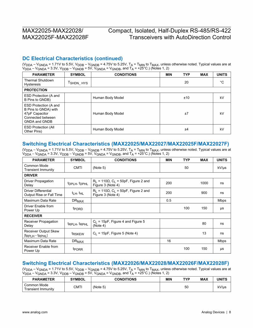
PARAMETER SYMBOL CONDITIONS MIN TYP MAX UNITS Thermal Shutdown Hysteresis TSHDN_ HYS 20 °C
PROTECTION ESD Protection (A and B Pins to GNDB) Human Body Model ±10 kV
ESD Protection (A and B Pins to GNDA) with 47pF Capacitor Connected between GNDA and GNDB
Human Body Model ±7 kV
ESD Protection (All Other Pins) Human Body Model ±4 kV
Switching Electrical Characteristics (MAX22025/MAX22027/MAX22025F/MAX22027F) (VDDA – VGNDA = 1.71V to 5.5V, VDDB – VGNDB = 4.75V to 5.25V, TA = TMIN to TMAX, unless otherwise noted. Typical values are at VDDA – VGNDA = 3.3V, VDDB – VGNDB = 5V, VGNDA = VGNDB, and TA = +25°C.) (Notes 1, 2)
PARAMETER SYMBOL CONDITIONS MIN TYP MAX UNITS Common Mode Transient Immunity CMTI (Note 5) 50 kV/μs
DRIVER Driver Propagation Delay tDPLH, tDPHL
RL = 110Ω, CL = 50pF, Figure 2 and Figure 3 (Note 4) 200 1000 ns
Driver Differential Output Rise or Fall Time tLH, tHL
RL = 110Ω, CL = 50pF, Figure 2 and Figure 3 (Note 4) 200 900 ns
Maximum Data Rate DRMAX 0.5 Mbps Driver Enable from Power Up tPORD 100 150 μs
RECEIVER Receiver Propagation Delay tRPLH, tRPHL
CL = 15pF, Figure 4 and Figure 5 (Note 4) 80 ns
Receiver Output Skew |tRPLH - tRPHL| tRSKEW CL = 15pF, Figure 5 (Note 4) 13 ns
Maximum Data Rate DRMAX 16 Mbps Receiver Enable from Power Up tPORR 100 150 μs
Switching Electrical Characteristics (MAX22026/MAX22028/MAX22026F/MAX22028F) (VDDA – VGNDA = 1.71V to 5.5V, VDDB – VGNDB = 4.75V to 5.25V, TA = TMIN to TMAX, unless otherwise noted. Typical values are at VDDA – VGNDA = 3.3V, VDDB – VGNDB = 5V, VGNDA = VGNDB, and TA = +25°C.) (Notes 1, 2)
PARAMETER SYMBOL CONDITIONS MIN TYP MAX UNITS Common Mode Transient Immunity CMTI (Note 5) 50 kV/μs
MAX22025-MAX22028/MAX22025F-MAX22028F
Compact, Isolated, Half-Duplex RS-485/RS-422Transceivers with AutoDirection Control
www.analog.com Analog Devices | 8

Switching Electrical Characteristics (MAX22026/MAX22028/MAX22026F/MAX22028F) (continued) (VDDA – VGNDA = 1.71V to 5.5V, VDDB – VGNDB = 4.75V to 5.25V, TA = TMIN to TMAX, unless otherwise noted. Typical values are at VDDA – VGNDA = 3.3V, VDDB – VGNDB = 5V, VGNDA = VGNDB, and TA = +25°C.) (Notes 1, 2)
PARAMETER SYMBOL CONDITIONS MIN TYP MAX UNITS DRIVER Driver Propagation Delay tDPLH, tDPHL
RL = 110Ω, CL = 50pF, Figure 2 and Figure 3 (Note 4) 50 ns
Driver Differential Output Rise or Fall Time tLH, tHL
RL = 110Ω, CL = 50pF, Figure 2 and Figure 3 (Note 4) 15 ns
Maximum Data Rate DRMAX 16 Mbps Driver Enable from Power Up tPORD 100 150 μs
RECEIVER Receiver Propagation Delay tRPLH, tRPHL
CL = 15pF, Figure 4 and Figure 5 (Note 4) 80 ns
Receiver Output Skew |tRPLH - tRPHL| tRSKEW CL = 15pF, Figure 5 (Note 4) 13 ns
Maximum Data Rate DRMAX 16 Mbps Receiver Enable from Power Up tPORR 100 150 μs
Note 1: All devices are 100% production tested at TA = +85°C. Specifications over temperature are guaranteed by design. Note 2: All currents into the device are positive. All currents out of the device are negative. All voltages are referenced to their
respective ground (GNDA or GNDB), unless otherwise noted. Note 3: This is the differential voltage from A to B that the driving device must see on the bus to disable its driver. Note 4: Not production tested. Guaranteed by design. Note 5: CMTI is the maximum sustainable common-mode voltage slew rate while maintaining the correct output states. CMTI applies
to both rising and falling common-mode voltage edges. Tested with the transient generator connected between GNDA and GNDB. VCM = 1kV
Insulation Characteristics PARAMETER SYMBOL CONDITIONS MIN TYP MAX UNITS
Maximum Repetitive Peak Withstand Voltage VIORM (Note 6) 630 VP
Maximum Working Isolation Voltage VIOWM GNDA to GNDB continuous (Note 6) 445 VRMS
Maximum Transient Isolation Voltage VIOTM 5000 VP
Maximum Withstand Isolation Voltage VISO GNDA to GNDB for 60s (Note 7) 3500 VRMS
Maximum Surge Isolation Voltage VIOSM
Basic Insulation, 1.2/50μs pulse per IEC61000-4-5 10 kV
Insulation Resistance RS TA = +150°C, VIO = 500V >109 Ω Barrier Capacitance Side A to Side B CIO GNDA to GNDB 2 pF
Minimum Creepage Distance CPG 5.5 mm
MAX22025-MAX22028/MAX22025F-MAX22028F
Compact, Isolated, Half-Duplex RS-485/RS-422Transceivers with AutoDirection Control
www.analog.com Analog Devices | 9

Insulation Characteristics (continued) PARAMETER SYMBOL CONDITIONS MIN TYP MAX UNITS
Minimum Clearance Distance CLR 5.5 mm
Internal Clearance Distance through insulation 0.015 mm Comparitive Tracking Resistance Index CTI >400
Climatic Category 40/125/21
Pollution Degree 2
Note 6: VIORM, VIOWM, and VISO are defined by the IEC 60747-5-5 standard.. Note 7: Product is qualified at VISO for 60 seconds. Not production tested.
RL2
RL2
VOC
VOD
A
B
(a)
375Ω
VCM
A
B
(b)
375Ω
+-
60ΩVOD
Figure 1. Driver DC Test Load
B
AVOD RL CL
TXD
Figure 2. Driver Timing Test Circuit
MAX22025-MAX22028/MAX22025F-MAX22028F
Compact, Isolated, Half-Duplex RS-485/RS-422Transceivers with AutoDirection Control
www.analog.com Analog Devices | 10

TXD
B
A
VOD
VDDA
GNDA
+VO
-VO
0
50% 50%
tDPLH tDPHL
VO
20%
80% 80%
20%
tLH tHL
tLH ≤ 3ns, tHL ≤ 3ns
tDSKEW = |tDPLH - tDPHL|
VDIFF = (VA - VB)
½ VO
½ VO
Figure 3. Driver Propagation Delays
ATE VID
A
B
RECEIVER OUTPUTRCL
Figure 4. Receiver Propagation Delay Test Circuit
A
B
VOH
RXDVOL
+1V
-1VtRPHL tRPLH
VDDA
tRSKEW = |tRPHL – tRPHL|
2
tHL ≤ 3ns, tLH ≤ 3ns
VDDA 2
Figure 5. Receiver Propagation Delays
MAX22025-MAX22028/MAX22025F-MAX22028F
Compact, Isolated, Half-Duplex RS-485/RS-422Transceivers with AutoDirection Control
www.analog.com Analog Devices | 11

Typical Operating Characteristics (VDDA – VGNDA = 3.3V, VDDB – VGNDB = 5V, VGNDA = VGNDB, and TA = +25°C, unless otherwise noted.)
MAX22025-MAX22028/MAX22025F-MAX22028F
Compact, Isolated, Half-Duplex RS-485/RS-422Transceivers with AutoDirection Control
www.analog.com Analog Devices | 12

Typical Operating Characteristics (continued) (VDDA – VGNDA = 3.3V, VDDB – VGNDB = 5V, VGNDA = VGNDB, and TA = +25°C, unless otherwise noted.)
MAX22025-MAX22028/MAX22025F-MAX22028F
Compact, Isolated, Half-Duplex RS-485/RS-422Transceivers with AutoDirection Control
www.analog.com Analog Devices | 13

Typical Operating Characteristics (continued) (VDDA – VGNDA = 3.3V, VDDB – VGNDB = 5V, VGNDA = VGNDB, and TA = +25°C, unless otherwise noted.)
MAX22025-MAX22028/MAX22025F-MAX22028F
Compact, Isolated, Half-Duplex RS-485/RS-422Transceivers with AutoDirection Control
www.analog.com Analog Devices | 14

Typical Operating Characteristics (continued) (VDDA – VGNDA = 3.3V, VDDB – VGNDB = 5V, VGNDA = VGNDB, and TA = +25°C, unless otherwise noted.)
Pin Configuration
MAX22025-MAX2208F
VDDB
B
A
GNDB
8
7
6
5
1
2
3
4
RXD
TXD
VDDA
GNDA
MAX22025-MAX22028/
MAX22025F-MAX22028F
WIDE SOIC
TOP VIEW
++
MAX22025-MAX22028/MAX22025F-MAX22028F
Compact, Isolated, Half-Duplex RS-485/RS-422Transceivers with AutoDirection Control
www.analog.com Analog Devices | 15
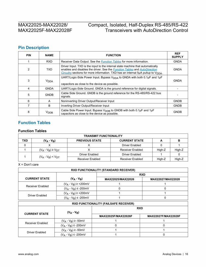
Pin Description PIN NAME FUNCTION REF
SUPPLY 1 RXD Receiver Data Output. See the Function Tables for more information. GNDA
2 TXD Driver Input. TXD is the input to the internal state machine that automatically enables and disables the driver. See the Function Tables and AutoDirection Circuitry sections for more information. TXD has an internal 5μA pullup to VDDA.
GNDA
3 VDDA UART/Logic-Side Power Input. Bypass VDDA to GNDA with both 0.1μF and 1μF
capacitors as close to the device as possible. GNDA
4 GNDA UART/Logic-Side Ground. GNDA is the ground reference for digital signals. -
5 GNDB Cable Side Ground. GNDB is the ground reference for the RS-485/RS-422 bus signals. -
6 A Noninverting Driver Output/Receiver Input GNDB 7 B Inverting Driver Output/Receiver Input GNDB
8 VDDB Cable Side Power Input. Bypass VDDB to GNDB with both 0.1μF and 1μF capacitors as close to the device as possible. GNDB
Function Tables
Function Tables TRANSMIT FUNCTIONALITY
TXD (VA - VB) PREVIOUS STATE CURRENT STATE A B 0 X X Driver Enabled 0 1 1 (VA - VB) ≥ VDT X Receiver Enabled High-Z High-Z
1 (VA - VB) < VDT Driver Enabled Driver Enabled 1 0
Receiver Enabled Receiver Enabled High-Z High-Z
X = Don’t care RXD FUNCTIONALITY (STANDARD RECEIVER)
CURRENT STATE (VA - VB) RXD
MAX22025/MAX22026 MAX22027/MAX22028
Receiver Enabled (VA - VB) ≥ +200mV 1 1 (VA - VB) ≤ -200mV 0 0
Driver Enabled (VA - VB) ≥ +200mV 1 1 (VA - VB) ≤ -200mV 1 0
RXD FUNCTIONALITY (FAILSAFE RECEIVER)
CURRENT STATE (VA - VB) RXD
MAX22025F/MAX22026F MAX22027F/MAX22028F
Receiver Enabled (VA - VB) ≥ -50mV 1 1
(VA - VB) ≤ -200mV 0 0
Driver Enabled (VA - VB) ≥ -50mV 1 1
(VA - VB) ≤ -200mV 1 0
MAX22025-MAX22028/MAX22025F-MAX22028F
Compact, Isolated, Half-Duplex RS-485/RS-422Transceivers with AutoDirection Control
www.analog.com Analog Devices | 16

Detailed Description The MAX22025-MAX22028/MAX22025F-MAX22028F isolated RS-485/RS-422 transceivers provide 3.5kVRMS (60s) of galvanic isolation between the RS-485/RS-422 cable side of the transceiver and the UART side. These devices allow up to 0.5Mbps (MAX22025/MAX22027/MAX22025F/MAX22027F) or 16Mbps (MAX22026/MAX22028/MAX22026F/MAX22028F) communication across an isolation barrier when a large potential exists between grounds on each side of the barrier.
Isolation Data isolation is achieved using high-voltage capacitors that allow data transmission between the UART side and the RS-485/RS-422 cable side of the transceiver. The devices withstand differences in ground potential between the two power domains of up to 3.5kVRMS (VISO) for up to 60s, and up to 445VRMS (VIOWM) for extended periods of time. See Table 1 for certification information.
Table 1. Safety Regulatory Approvals UL The MAX22025-MAX22028 and MAX22025F-MAX22028F are certified under UL1577. For more details, refer to File E351759. Rated up to 3500VRMS for single protection. cUL (Equivalent to CSA notice 5A) The MAX22025-MAX22028 and MAX22025F-MAX22028F are certified up to 3500VRMS for single protection. For more details, refer to File E351759.
AutoDirection Circuitry Internal circuitry in the MAX22025-MAX22028/MAX22025F-MAX22028F, in conjunction with an external pullup resistor on A and pulldown resistor on B (see Typical Application Circuit), acts to automatically disable or enable the driver and the receiver to keep the bus in the correct state. This Auto Direction circuitry consists of a state machine and an additional receive comparator that determine whether this device is trying to drive the bus or another node on the network is driving the bus. The internal state machine has two inputs: TXD The current state of (VA-VB), which is determined by a dedicated differential comparator. The state machine also has two outputs: DRIVER_ENABLE—Internal signal that enables and disables the driver RECEIVER_ENABLE—Internal signal that is the inverse of the DRIVER_ENABLE signal. When TXD is low, the device always drives the bus low. When TXD switches high, the device drives the bus for a short time, then disables the driver and allows the external pullup/pulldown resistors to hold the bus in the high state. During each low-to-high transition of TXD, the driver stays enabled until (VA-VB) ≥ VDT. The driver is then disabled and the pullup/pulldown resistors hold the A and B lines in the correct state.
Pullup and Pulldown Resistors The pullup and pulldown resistors on the A and B lines are required for proper operation of the device although their exact value is not critical. They function to hold the bus in the high state following a low-to-high transition. Sizing of these resistors is determined in the same way as when using any other RS-485 driver and depends on how the line is terminated and how many nodes are on the bus. The most important factor when sizing these resistors is to guarantee that the idle voltage on the bus (VA-VB) is greater than the receiver input threshold (+200mV for the MAX22025-MAX22028, -50mV for the MAX22025F-MAX22028F) in order to remain compatible with standard RS-485 receiver thresholds.
MAX22025-MAX22028/MAX22025F-MAX22028F
Compact, Isolated, Half-Duplex RS-485/RS-422Transceivers with AutoDirection Control
www.analog.com Analog Devices | 17

Receive State When not transmitting data, the MAX22025-MAX22028/MAX22025F-MAX22028F require the TXD input be high to remain in the receive state. A conventional RS-485 transceiver has DE and RE inputs that are used to enable and disable the driver and receiver. However, the MAX22025-MAX22028/MAX22025F-MAX22028F do not have a DE input, and instead use an internal state machine to enable and disable the drivers.
Failsafe Receiver (MAX22025F-MAX22028F only) The MAX22025F-MAX22028F guarantee a logic high on the receiver output when the receiver inputs are shorted or open, or when they are connected to a terminated transmission line with all drivers disabled. If the differential receiver input voltage (VA - VB) is greater than or equal to -50mV, RXD is a logic-high.
Receiver Output (RXD) The receiver output (RXD) of the MAX22025/MAX22026/MAX22025F/MAX22026F does not follow TXD when the device is in the driver-enabled state. This allows for line interference detection by verifying that RXD remains high throughout data transmission. On the MAX22027/MAX22028/MAX22027F/MAX22028F, the receiver output (RXD) always follows (VA-VB).
ESD Protection ESD protection structures are incorporated on all pins to protect against electrostatic discharge encountered during handling and assembly. The driver outputs and receiver inputs of the devices have extra protection against static electricity to both the UART side and cable side ground references. The ESD structures withstand high-ESD events during normal operation and when powered down. After an ESD event, the devices keep working without latch-up or damage. Bypass VDDA to GNDA and bypass VDDB to GNDB with 0.1μF and 1μF capacitors to ensure maximum ESD protection.
ESD Test Conditions ESD performance depends on a variety of conditions. Contact Maxim for a reliability report that documents test setup, test methodology, and test results.
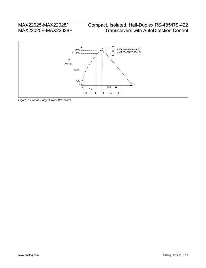
Human Body Model (HBM) Figure 6 shows the HBM test model, while Figure 7 shows the current waveform it generates when discharged in a low-impedance state. This model consists of a 100pF capacitor charged to the ESD voltage of interest, which is then discharged into the test device through a 1.5kΩ resistor.
HIGH-VOLTAGE
DC SOURCE
DEVICE UNDERTEST
RC1MW
RD1.5kW
CS100pF
CHARGE CURRENT-LIMIT RESISTOR
DISCHARGE RESISTANCE
STORAGECAPACITOR
Figure 6. Human Body ESD Test Model
MAX22025-MAX22028/MAX22025F-MAX22028F
Compact, Isolated, Half-Duplex RS-485/RS-422Transceivers with AutoDirection Control
www.analog.com Analog Devices | 18
AMPERES
100%90%
10%
tRL
tDL
IP
36.8%
IRPEAK-TO-PEAK RINGING(NOT DRAWN TO SCALE)
00 TIME
Figure 7. Human Body Current Waveform
MAX22025-MAX22028/MAX22025F-MAX22028F
Compact, Isolated, Half-Duplex RS-485/RS-422Transceivers with AutoDirection Control
www.analog.com Analog Devices | 19

Typical Application Circuits
Typical Application Circuit 1
MICR
CONT
ROLL
ER MAX22025-MAX22028/
MAX22025F-MAX22028F
VCC
VDDA
RXD
TXD
11
RX
TX
3.3V 5V
VDDBRPU
RT
RPD
MICRCONTROLLER
MAX22025-MAX22028/
MAX22025F-MAX22028F
VCC
VDDA
RXD
TXD
44
RX
TX
3.3V5V
VDDBRPU
RT
RPD
22 3
3
A
B
A
B
Typical Application Circuit 2
RXD
TXD
RS-4
85 T
RANS
CEIV
ER A
B
RXDRE
TXD
DE
RS-485 TRANSCEIVER
A
B
RXDTXD
RS-485 TRANSCEIVER
AB
RXDTXD
RS-485 TRANSCEIVER
AB
INTEGRATED ISOLATION BARRIER
MAX22025-MAX22028MAX22025F-MAX22028F
Master/Slave Master/Slave
Master/Slave
Master/Slave
1 22
VPU
nn-1n-1
VPU
MAX22025-MAX22028/MAX22025F-MAX22028F
Compact, Isolated, Half-Duplex RS-485/RS-422Transceivers with AutoDirection Control
www.analog.com Analog Devices | 20
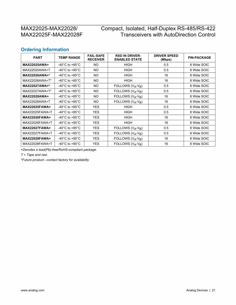
Ordering Information PART TEMP RANGE FAIL-SAFE
RECEIVER RXD IN DRIVER-
ENABLED STATE DRIVER SPEED
(Mbps) PIN-PACKAGE
MAX22025AWA+ -40°C to +85°C NO HIGH 0.5 8 Wide SOIC MAX22025AWA+T -40°C to +85°C NO HIGH 0.5 8 Wide SOIC MAX22026AWA+* -40°C to +85°C NO HIGH 16 8 Wide SOIC MAX22026AWA+T* -40°C to +85°C NO HIGH 16 8 Wide SOIC MAX22027AWA+* -40°C to +85°C NO FOLLOWS (VA-VB) 0.5 8 Wide SOIC MAX22027AWA+T* -40°C to +85°C NO FOLLOWS (VA-VB) 0.5 8 Wide SOIC MAX22028AWA+ -40°C to +85°C NO FOLLOWS (VA-VB) 16 8 Wide SOIC MAX22028AWA+T -40°C to +85°C NO FOLLOWS (VA-VB) 16 8 Wide SOIC MAX22025FAWA+ -40°C to +85°C YES HIGH 0.5 8 Wide SOIC MAX22025FAWA+T -40°C to +85°C YES HIGH 0.5 8 Wide SOIC MAX22026FAWA+ -40°C to +85°C YES HIGH 16 8 Wide SOIC MAX22026FAWA+T -40°C to +85°C YES HIGH 16 8 Wide SOIC MAX22027FAWA+ -40°C to +85°C YES FOLLOWS (VA-VB) 0.5 8 Wide SOIC MAX22027FAWA+T -40°C to +85°C YES FOLLOWS (VA-VB) 0.5 8 Wide SOIC MAX22028FAWA+ -40°C to +85°C YES FOLLOWS (VA-VB) 16 8 Wide SOIC MAX22028FAWA+T -40°C to +85°C YES FOLLOWS (VA-VB) 16 8 Wide SOIC
+Denotes a lead(Pb)-free/RoHS-compliant package. T = Tape and reel. *Future product—contact factory for availability
MAX22025-MAX22028/MAX22025F-MAX22028F
Compact, Isolated, Half-Duplex RS-485/RS-422Transceivers with AutoDirection Control
www.analog.com Analog Devices | 21

Revision History REVISION NUMBER
REVISION DATE DESCRIPTION PAGES
CHANGED 0 8/19 Initial release —
1 9/19 Updated the Electrical Characteristics section and added future product designation to MAX22025AWA+ and MAX22025AWA+T in the Ordering Information table 3, 15
2 11/19 Removed future product designation from MAX22025AWA+ and MAX22025AWA+T in the Ordering Information table 15
3
2/20
Updated the title, General Description, Benefits and Features, Functional Diagram, DC Electrical Characteristics, Swtiching Electrical Characteristics, Pin Configuration, Functional Tables, Detailed Description, AutoDirection Circuitry, Pullup and Pulldown Resistors, Receive State, Receiver Output (RXD), and Typical Application Circuits sections; updated TOC01–TOC14, TOC23–TOC32; added the Safety Regulatory Approvals table and Failsafe Receiver (MAX22025F–MAX22028F) section; added MAX22025FAWA+, MAX22025FAWA+T, MAX22026FAWA+, MAX22026FAWA+T, MAX22027FAWA+, MAX22027FAWA+T, MAX22028FAWA+, and MAX22028FAWA+T as future parts to the Ordering Information table
1–16
3.1 Corrected typo 1
4 4/20 Removed future product designation from MAX22025FAWA+ and MAX22025FAWA+T in the Ordering Information table 15
5 3/21 Removed future product designation from MAX22028FAWA+ and MAX22028FAWA+T and added a Fail-Safe Receiver column in the Ordering Information table 19
6 3/21 Removed future product designation from MAX22026FAWA+, MAX22026FAWA+T, MAX22027FAWA+, and MAX22027FAWA+T in the Ordering Information table and updated the Isolation and Receiver Output (RXD) sections
15, 16, 19
Information furnished by Analog Devices is believed to be accurate and reliable. However, no responsibility is assumed by Analog Devices for its use, nor for any infringements of patents or other rights of third parties that may result from its use. Specifications subject to change without notice. No license is granted by implication or otherwise under any patent or patent rights of Analog Devices. Trademarks andregistered trademarks are the property of their respective owners.
MAX22025-MAX22028/MAX22025F-MAX22028F
Compact, Isolated, Half-Duplex RS-485/RS-422Transceivers with AutoDirection Control
w w w . a n a l o g . c o m Analog Devices | 22