Embed Size (px)
Citation preview
1482 IEEE JOURNAL OF SOLID-STATE CIRCUITS, VOL. 33, NO. 10, OCTOBER 1998
Compact Low-Voltage Power-EfficientOperational Amplifier Cells for VLSI
Klaas-Jan de Langen,Member, IEEE, and Johan H. Huijsing,Fellow, IEEE
Abstract— Compact low-voltage power-efficient operationalamplifiers are described that are very suitable as very-large-scale-integration library cells because of the small die area of0.08 mm2 and the minimum supply voltage of 1.8 V. A keypart of the circuit is the rail-to-rail class-AB output stage withfolded mesh feedback control that combines power efficiencywith operation down to 1.8 V and allows sufficient gain in acompact two-stage topology. A version with rail-to-rail inputstage features a rail-to-rail input range for supply voltages downto 2.5 V. The dc gain of the op-amps is more than 80 dB whiledriving 10 k, and the unity-gain frequency is 4 MHz withphase margin of 67� while driving 5 pF. The equivalent inputnoise voltage is 38 nV/
pHz at a frequency of 100 kHz. The
amplifiers have been implemented in a standard digital 1.6-�mcomplementary metal–oxide–semiconductor process.
Index Terms—Analog integrated circuits, CMOS integratedcircuits, operational amplifiers, very-large-scale integration.
I. INTRODUCTION
A PPLYING simple topologies in order to obtain highefficiency is the key design technique for future ana-
log cells in mixed-mode very-large-scale-integration (VLSI)circuits. As the reduction in feature size of complemen-tary metal–oxide–semiconductor (CMOS) processes continuessteadily, the supply voltage has to be reduced while the higherintegration density enforces lower power consumption per cell.Digital cells benefit from the size reduction, yielding improveddigital performance. Analog cells, on the other hand, onlybenefit marginally because minimum size transistors cannotbe used due to noise and offset requirements. Further, thelow supply voltage complicates the design, yielding oftenmore complex circuit solutions, which may even result ina performance reduction. The only way for analog cells tokeep up with the digital performance and the supply-voltagereduction is by using very efficient topologies that combinelow-voltage operation with high power efficiency and smalldie area.
Existing op-amps can either operate well below 3 V butuse a complex structure [1], [2] or employ a simple two-stagetopology [3]–[5] but require a supply voltage of the order of2.7–3.0 V depending on technology. However, as is shown inSection II, the minimum required supply voltage for a compacttwo-stage op-amp is equal to one gate-source voltage and twosaturation voltages, which is of the order of 1.6–2.0 V. This
Manuscript received June 18, 1997; revised March 30, 1998. This workwas supported by the Technology Foundation.
The authors are with the Delft Institute of Microelectronics and SubmicronTechnology, Delft University of Technology, Delft 2628 CD The Netherlands.
Publisher Item Identifier S 0018-9200(98)06996-0.
is only one saturation voltage more than the ultimate lowestsupply voltage. But this lowest limit can only be obtainedby using at least four stages [2]. The subject of this paperis to develop an amplifier topology that combines operationdown to a supply voltage equal to one gate-source voltage andtwo saturation voltages using a compact two-stage structureoffering high power efficiency and small die area.
In Section II the basic low-voltage compact topology ispresented. Thereafter, low-voltage class-AB control circuitsare discussed, and a suitable control circuit is selected inSection III. In Section IV, the low-voltage topology is ex-tended to allow an optional rail-to-rail input stage. Two op-ampimplementations are presented in Section V, together with themeasurement results. In Section VI, conclusions are drawn.
II. L OW-VOLTAGE COMPACT TOPOLOGY
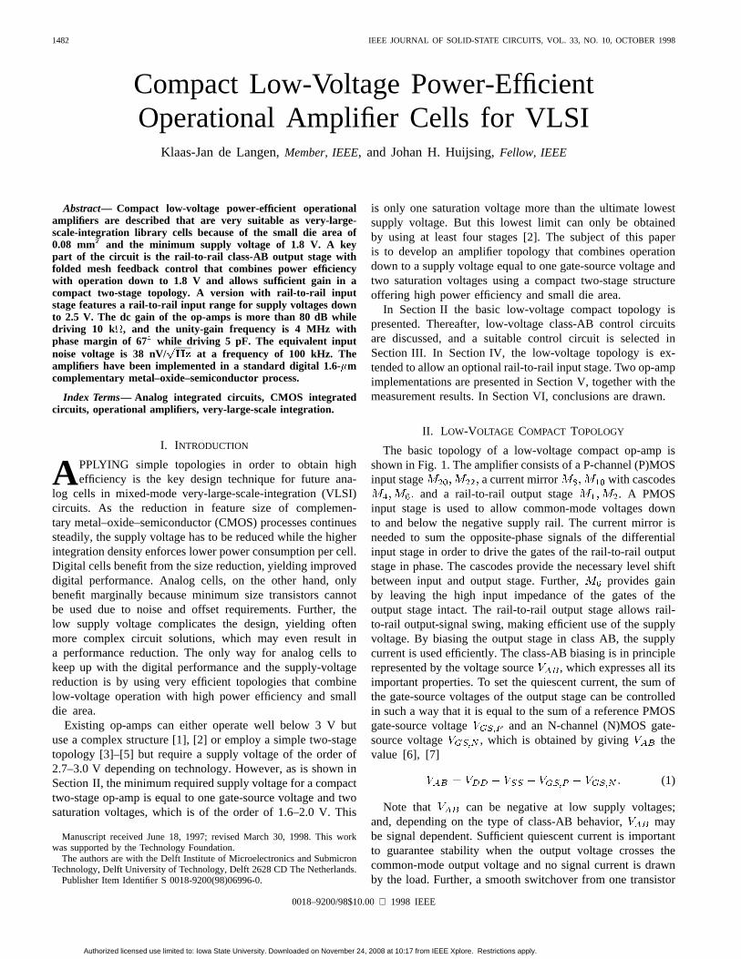
The basic topology of a low-voltage compact op-amp isshown in Fig. 1. The amplifier consists of a P-channel (P)MOSinput stage a current mirror with cascodes
and a rail-to-rail output stage . A PMOSinput stage is used to allow common-mode voltages downto and below the negative supply rail. The current mirror isneeded to sum the opposite-phase signals of the differentialinput stage in order to drive the gates of the rail-to-rail outputstage in phase. The cascodes provide the necessary level shiftbetween input and output stage. Further, provides gainby leaving the high input impedance of the gates of theoutput stage intact. The rail-to-rail output stage allows rail-to-rail output-signal swing, making efficient use of the supplyvoltage. By biasing the output stage in class AB, the supplycurrent is used efficiently. The class-AB biasing is in principlerepresented by the voltage source , which expresses all itsimportant properties. To set the quiescent current, the sum ofthe gate-source voltages of the output stage can be controlledin such a way that it is equal to the sum of a reference PMOSgate-source voltage and an N-channel (N)MOS gate-source voltage , which is obtained by giving thevalue [6], [7]
(1)
Note that can be negative at low supply voltages;and, depending on the type of class-AB behavior, maybe signal dependent. Sufficient quiescent current is importantto guarantee stability when the output voltage crosses thecommon-mode output voltage and no signal current is drawnby the load. Further, a smooth switchover from one transistor
0018–9200/98$10.00 1998 IEEE
Authorized licensed use limited to: Iowa State University. Downloaded on November 24, 2008 at 10:17 from IEEE Xplore. Restrictions apply.
DE LANGEN AND HUIJSING: AMPLIFIER CELLS FOR VLSI 1483
Fig. 1. Compact low-voltage operational amplifier principle.
to the other is obtained, avoiding gross crossover distortion,because the output transistors are gradually switched on andoff. A final property is that the signal from cascode isdistributed over the two output transistors in such a way thatall the signal contributes to the output voltage independent ofwhich transistor is active. By biasing the class-AB controlcircuit by the current mirror, no extra current is neededand no extra noise and offset are generated by adding theclass-AB function. Because of the simple two-stage topology,Miller compensation is sufficient to compensate the op-ampas indicated by Miller capacitors and , whichare connected across each output transistor. Thus, no difficultcompensation scheme is needed that would require largebandwidth reduction or more bias current in the output stage.
The minimum supply voltage is in general limited by theoutput stage because it needs to drive high output currentsrequiring large gate-source voltages. The supply voltage ofthe output stage is equal to the sum of the gate-source voltageof the voltage and the gate-source voltage of
, as can be concluded from Fig. 1. Since can benegative, theoretically, the minimum supply voltage neededby the output stage can be very small. Practically, however,the gate of an output transistor is always at least connectedvia a current source to the supply rails. Because we need toobtain sufficient gain in only two stages, the current sourceshould not deteriorate the impedance and must be cascoded.To allow the lowest possible supply voltage, the transistors ofthe current source should be biased at the edge of the trioderegion, resulting in a minimum supply voltage limited by agate-source voltage and two saturation voltages.
Concluding, each component of the compact op-amp shownin Fig. 1 has at least one important function: proving thehigh efficiency in terms of the number of components. Be-cause of the low number of components and the two-stagetopology, which can be efficiently compensated using Millercompensation, a relatively small bias current is required.
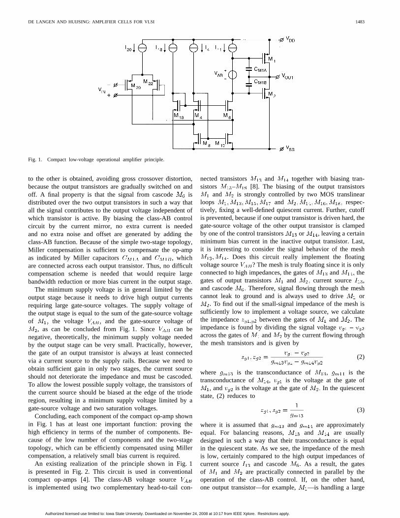
An existing realization of the principle shown in Fig. 1is presented in Fig. 2. This circuit is used in conventionalcompact op-amps [4]. The class-AB voltage sourceis implemented using two complementary head-to-tail con-
nected transistors and together with biasing tran-sistors – [8]. The biasing of the output transistors
and is strongly controlled by two MOS translinearloops and respec-tively, fixing a well-defined quiescent current. Further, cutoffis prevented, because if one output transistor is driven hard, thegate-source voltage of the other output transistor is clampedby one of the control transistors or , leaving a certainminimum bias current in the inactive output transistor. Last,it is interesting to consider the signal behavior of the mesh
Does this circuit really implement the floatingvoltage source ? The mesh is truly floating since it is onlyconnected to high impedances, the gates of and thegates of output transistors and current source ,and cascode Therefore, signal flowing through the meshcannot leak to ground and is always used to drive or
To find out if the small-signal impedance of the mesh issufficiently low to implement a voltage source, we calculatethe impedance between the gates of and Theimpedance is found by dividing the signal voltageacross the gates of and by the current flowing throughthe mesh transistors and is given by
(2)
where is the transconductance of , is thetransconductance of , is the voltage at the gate of
, and is the voltage at the gate of In the quiescentstate, (2) reduces to
(3)
where it is assumed that and are approximatelyequal. For balancing reasons, and are usuallydesigned in such a way that their transconductance is equalin the quiescent state. As we see, the impedance of the meshis low, certainly compared to the high output impedances ofcurrent source and cascode As a result, the gatesof and are practically connected in parallel by theoperation of the class-AB control. If, on the other hand,one output transistor—for example, —is handling a large
Authorized licensed use limited to: Iowa State University. Downloaded on November 24, 2008 at 10:17 from IEEE Xplore. Restrictions apply.
1484 IEEE JOURNAL OF SOLID-STATE CIRCUITS, VOL. 33, NO. 10, OCTOBER 1998
Fig. 2. Conventional compact two-stage operational amplifier with rail-to-rail feed-forward class-AB output stage with mesh.
Fig. 3. Low-voltage compact two-stage operational amplifier with rail-to-rail feed-forward class-AB output stage with level shift in mesh.
output current, the other output transistor is regulated ata constant minimum current. Coupling of the gates of the twooutput transistors using a mesh with low impedance is notpossible because handles all the signal and has a largesignal swing at its gate, while has a constant gate-sourcevoltage. Consequently, the small-signal voltageat the gateof is very small. Because the gate-source voltage ofislarge, is off and its transconductance is very small. Using(2), it can be concluded that the mesh impedance is very large,so that there is no coupling between the two gates of the outputtransistors. However, transistor is still active, operatingas a cascode that steers all the signal current delivered byto the active output transistor Summarizing, the class-ABcontrol circuit couples the gates of the output transistors in thequiescent mode of operation by generating a low impedance.When one output transistor delivers a large output current,the other output transistor is regulated at a constant draincurrent and the gates of the output transistors are decouplingby generating a large impedance. At the same time, however,
the class-AB control circuit steers all the signal to the activeoutput transistor.
Another important property of the class-AB control circuitis the contribution to the noise and offset. Fortunately, theclass-AB control transistors and are biased by usingthe bias current, which is already needed to bias the summingcircuit and Therefore, no additionalbias-current sources are required that would increase the noiseand offset and also would reduce the gain [4]. The remainingdisadvantage of the circuit is that the minimum supply voltageis equal to two gate-source voltages and one saturation voltage.For example, we need to bias the gate-source voltages ofand and sufficient voltage across current sourceinsidethe supply voltage.
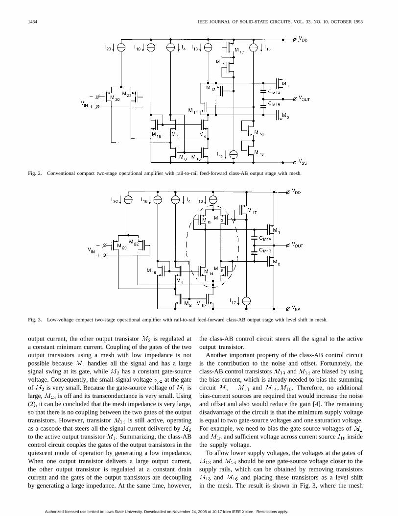
To allow lower supply voltages, the voltages at the gates ofand should be one gate-source voltage closer to the
supply rails, which can be obtained by removing transistorsand and placing these transistors as a level shift
in the mesh. The result is shown in Fig. 3, where the mesh
Authorized licensed use limited to: Iowa State University. Downloaded on November 24, 2008 at 10:17 from IEEE Xplore. Restrictions apply.
DE LANGEN AND HUIJSING: AMPLIFIER CELLS FOR VLSI 1485
Fig. 4. Low-voltage compact two-stage operational amplifier with rail-to-rail feedback class-AB output stage with folded mesh and class-AB control.
is indicated by the dashed line. The mesh now consists oftransistors and and diode-connected transistorsand The output transistors are biased by MOS translinearloops and Some ofthe properties of the previous circuit are maintained. However,the diode level shifts introduce two problems. First, cutoff ofthe output transistors occurs when the output stage is drivenhard. If, for example, delivers a high output current, itsgate-source voltage is large and all the current in the meshflows through and while no current flows through
and The voltage across is very small, andtherefore the gate-source voltage of is small and cutoffoccurs. A second problem is that there is almost no roomto bias the current source and transistor This isespecially so when we note that the output transistors usuallyhave large ratios in order to drive large output currents.Therefore, in the quiescent state, the gate-source voltage ofthe output transistors is relatively small, and room forand can only be created by making the ratio of
and very large. There is certainly noroom to insert cascodes. Due to the diode connection,and
also do not function as a cascode, so that the obtainablegain is too low in a two-stage topology.
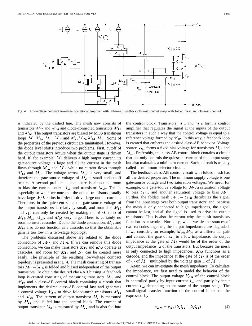
The problems discussed above are related to the diodeconnection of and If we can remove this diodeconnection, we can make transistors and operate ascascodes, and room for and can be created moreeasily. The principle of the resulting low-voltage compacttopology is presented in Fig. 4. The mesh consisting of transis-tors is folded and biased independent of the outputtransistors. To obtain the desired class-AB biasing, a feedbackloop is created consisting of measuring transistors and
and a class-AB control block containing a circuit thatimplements the desired class-AB control law and generatesa control voltage to drive folded-mesh transistorsand The current of output transistor is measuredby and is fed into the control block. The current ofoutput transistor is measured by and is also fed into
the control block. Transistors and form a controlamplifier that regulates the signal at the inputs of the outputtransistors in such a way that the control voltage is equal to areference voltage formed by In this way, a feedback loopis created that enforces the desired class-AB behavior. Voltagesource forms a fixed bias voltage for transistors and
Preferably, the class-AB control block contains a circuitthat not only controls the quiescent current of the output stagebut also maintains a minimum current. Such a circuit is usuallycalled a minimum selector circuit.
The feedback class-AB control circuit with folded mesh hasall the desired properties. The minimum supply voltage is onegate-source voltage and two saturation voltages. We need, forexample, one gate-source voltage for a saturation voltageto bias and another saturation voltage to biasFurther, the folded mesh distributes the signalfrom the input stage over both output transistors; and, becausethe mesh is only connected to high impedances, the signalcannot be lost, and all the signal is used to drive the outputtransistors. This is also the reason why the mesh transistorsfunction as cascodes. Normally, when we tie the sources oftwo cascodes together, the output impedances are degraded.If we consider, for example, as a differential pairand connect the gate of to a low impedance, the outputimpedance at the gate of would be of the order of theoutput impedance of the transistors. But because the meshis only connected to high impedances, functions as acascode, and the impedance at the gate ofis of the orderof of multiplied by the voltage gain of
Again, we can investigate the mesh impedance. To calculatethe impedance, we first need to model the behavior of thecontrol block. The output voltage of the control blockis controlled partly by input current and partly by inputcurrent depending on the state of the output stage. Thesmall-signal transfer function of the control block can beexpressed by
(4)
Authorized licensed use limited to: Iowa State University. Downloaded on November 24, 2008 at 10:17 from IEEE Xplore. Restrictions apply.
1486 IEEE JOURNAL OF SOLID-STATE CIRCUITS, VOL. 33, NO. 10, OCTOBER 1998
where represents the current-to-voltage conversion of thecontrol block, and and are variables that depend onthe state of the output stage and determine the influence of thesmall-signal input currents and on the class-AB controlvoltage. In the quiescent state, the control voltage is equallycontrolled by and , and and are equal. To findthe values of and , we should consider an example of aminimum selector circuit. A suitable example having a simpletransfer function is the conventional bipolar minimum selectorcircuit [9]. The class-AB characteristic of the conventionalcircuit is described by
(5)
which also describes the CMOS version of the circuit operatingin weak inversion. The transfer function of the minimumselector circuit used to implement the class-AB behavior asdescribed by (5) is given by
(6)
where is the output current of the minimum selectorcircuit. Examining (6) for small signals yields
(7)
In the quiescent state, and are equal. By comparing(7) with (4), we conclude that and are equal to in thiscase. If one output transistor—for example, —is handlinga large output current, the class-AB circuit only controls thebiasing of the other one, and therefore is zero and isone. This can also be concluded by examining (7) and notingthat is much larger than in this case.
We now return to the main problem of calculating the meshimpedance. By examining the remaining part of the controlloop consisting of differential pair and transistors
and and using (4), the mesh impedance isfound as
(8)
where is the transconductance of , is thetransconductance of , and is the transconductance ofclass-AB control amplifier In the quiescent state,
and are both equal to , and for balancing reasons, thetransconductance of transistors and is equal, yielding
(9)
which confirms the low impedance of the mesh. When oneoutput transistor is delivering a large output current—forexample, —the voltage at the gate is regulated constant sothat is very small. Further, is zero, and thus the meshimpedance is very large. All the signal current generated by
and is steered by cascode to the active outputtransistor or by cascodes
It is interesting to consider the contribution of the meshtransistors to the noise and offset. In the same way as in the
conventional circuit, the mesh transistors use the bias currentof the summing circuit. Therefore, no additional bias currentis required, and no extra noise or offset is generated. Thedifferential pair may give reason for concern sincedifferential-pair transistors normally contribute to the noise.However, these transistors operate only as differential pairs forclass-AB signals, which do not contribute to the output signal.For normal signals, the mesh transistors operate as cascodes,which do not contribute to the noise.
Because a feedback loop is used to implement the class-AB control, also the stability of the class-AB loop should beconsidered. The loop consists of class-AB amplifiermeasuring transistors and and the class-AB controlblock. Basically, the class-AB loop can be considered as asingle-stage amplifier with transconductance stageand with the Miller capacitors and the gate-source capacitorsas load capacitors. Since the output transistors are driven outof phase by the class-AB amplifier, there is no class-AB signalvoltage at the output node. Therefore, the Miller capacitors canbe considered as if they are connected to ground in parallelwith the gate-source capacitance. The unity-gain frequency ofthe class-AB loop is therefore given by
(10)
where is the gate-source capacitance of transistorand is the gate-source capacitance of transistor Inthe quiescent state, and are both equal to , yielding
(11)
where it is assumed that the transconductance of andare equal and the capacitance terms and
are equal. The gate-source capacitances ofthe two output transistors are normally not equal; however,the Miller capacitors have usually relatively large values, andtherefore the capacitance terms can be assumed to be equalin a first-order approximation. When one output transistoris handling a large current—for example, —the class-ABcontrol circuit is controlling the minimum current of the otheroutput transistor. Then is one and is zero, and theunity-gain frequency is given by
(12)
which is a factor of two larger than the value given by (11) inthe quiescent state. However, it should be noted that isbiased by a current that is a factor of two smaller than in thequiescent state. Therefore, in bipolar technology and in CMOStechnology with transistors operating in weak inversionis a factor of two smaller, and the unity-gain frequency isindependent of the state of the output stage. In CMOS withtransistors operating in strong inversion, the transconductancechanges only by a factor of , and therefore the bandwidthis a factor of larger than in the quiescent state. To assure
Authorized licensed use limited to: Iowa State University. Downloaded on November 24, 2008 at 10:17 from IEEE Xplore. Restrictions apply.
DE LANGEN AND HUIJSING: AMPLIFIER CELLS FOR VLSI 1487
that the biasing of the output transistors is controlled over thewhole bandwidth, the unity-gain frequency of the class-ABloop should be larger than the unity-gain frequency of the mainamplifier. However, the unity-gain frequency of the class-ABloop should be fixed at a frequency well below the parasiticpoles of the minimum selector circuit in order to obtain astable class-AB loop. Concluding, when using CMOS in stronginversion, the bandwidth of the class-AB loop is the smallestin the quiescent state, and therefore it should be checked in thequiescent state if the bandwidth is sufficient. In which state thephase margin is minimum depends on the implementation ofthe minimum selector, and this is discussed in the next section,where the minimum-selector circuits are discussed. As can beconcluded from (11) and (12), the bandwidth of the class-ABloop can be manipulated by adjusting the transconductance
of the class-AB amplifier.Concluding, we have found a low-voltage compact op-amp
topology with the same properties as the conventional op-amp topology. Good class-AB behavior is obtained withoutreducing the gain and without extra noise contribution, butwith operation down to lower supply voltages of one gate-source voltage and two saturation voltages. We now haveto find suitable minimum-selector circuits that can operate atthese low supply voltages. This will be considered in the nextsection.
III. L OW-VOLTAGE OP-AMP IMPLEMENTATION
A. Minimum-Selector Circuit
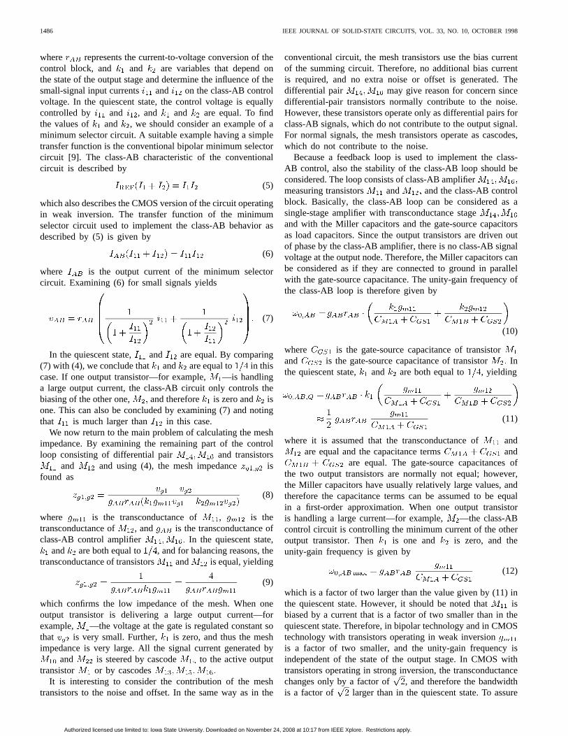
A class of well-known reliable class-AB control circuitsuses a decision pair to control the minimum bias currentin the output stage [9]. A low-voltage CMOS version ofthis circuit uses a PMOS decision pair in combination withan NMOS control amplifier [10]. A disadvantage of thisarrangement is the bad matching between PMOS gate-sourcevoltage and NMOS gate-source voltage, which makes thiscircuit unreliable at very low supply voltages [7]. A solutionto this problem is to replace the PMOS decision pair byan NMOS diode-coupled decision pair. The result is a firstcomplete implementation of a folded-mesh class-AB outputstage, as shown in Fig. 5. As indicated in the figure by theinput currents and , the input signal can be fed intothe sources of the PMOS mesh transistors as well as into thesources of the NMOS mesh transistors. The current ofismeasured by and is used to generate a voltage acrossThe current of is measured by flows through mirror
and generates a voltage across The lower ofthe two voltages across the resistors, which corresponds to thelower of the bias currents of the output transistors, controlsthe output of the decision pair which is connectedto the gate of This voltage steers the class-AB amplifier
, which is part of the previously discussed mesh. Theamplifier regulates the control voltage equal to a referencevoltage created by and by controlling the signalat the gates of the output transistors. Thus, a feedback loopis created that controls the minimum current of the outputtransistors. By using an NMOS diode-coupled decision pair,
(a)
(b)
Fig. 5. Low-voltage feedback class-AB output stage with folded mesh anddiode-coupled minimum selector. (a) Circuit. (b) Class-AB characteristic.
the voltage across current sourceis accurately determinedby the voltage across The voltage across is veryimportant because it must be sufficient to allowto functionproperly, but it must be as small as possible to allow lowsupply voltages. The minimum supply voltage of the outputstage is equal to the sum of the gate-source voltage ofthe voltage across and the minimum voltage required tobias in saturation. However, a drawback is that care mustbe taken to obtain a well-defined minimum current. As can beconcluded from the relation between minimum currentand quiescent current
(13)
where and are the currents of the current sourcesas indicated in Fig. 5(a), should be taken small, andand should be taken large to obtain sufficient minimumcurrent. The resulting class-AB characteristic is depicted inFig. 5(b). The need for large resistors is the main disadvantageof this circuit, since accurate large resistors are not alwaysavailable in CMOS processes and require a large die area.
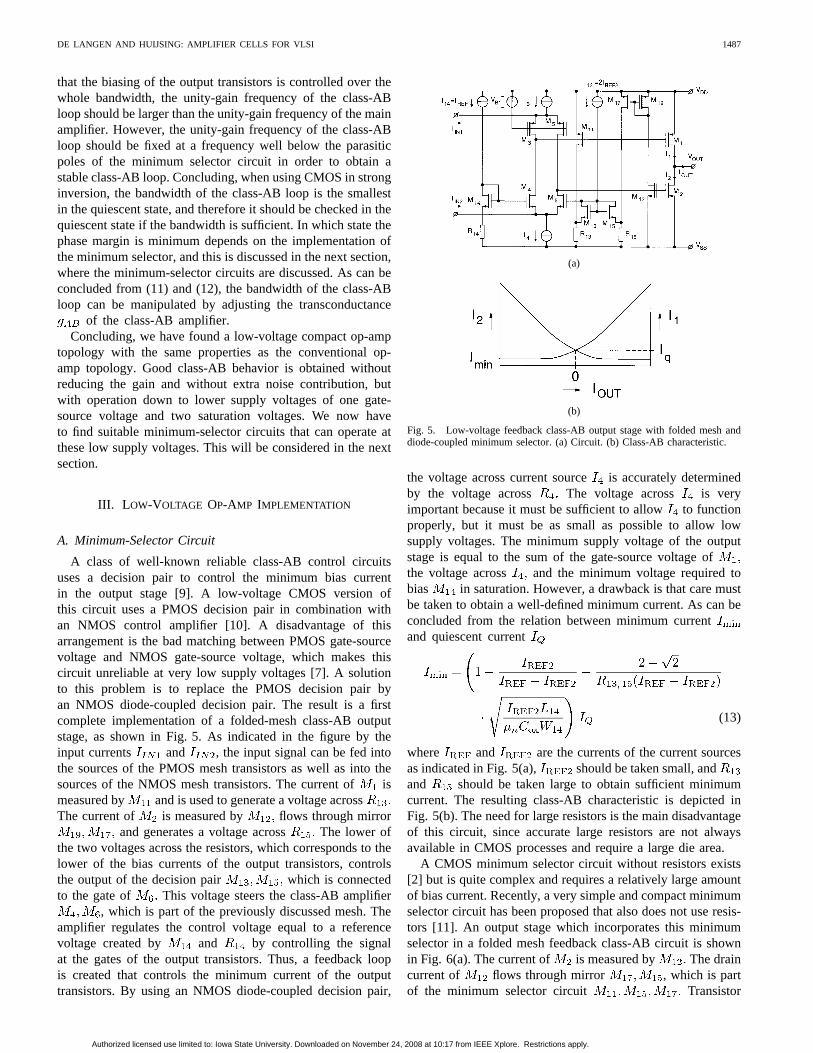
A CMOS minimum selector circuit without resistors exists[2] but is quite complex and requires a relatively large amountof bias current. Recently, a very simple and compact minimumselector circuit has been proposed that also does not use resis-tors [11]. An output stage which incorporates this minimumselector in a folded mesh feedback class-AB circuit is shownin Fig. 6(a). The current of is measured by The draincurrent of flows through mirror , which is partof the minimum selector circuit Transistor
Authorized licensed use limited to: Iowa State University. Downloaded on November 24, 2008 at 10:17 from IEEE Xplore. Restrictions apply.
1488 IEEE JOURNAL OF SOLID-STATE CIRCUITS, VOL. 33, NO. 10, OCTOBER 1998
of the minimum selector circuit operates mainly in thelinear region. Only when handles large output current does
operate in saturation. measures the current ofand is also part of the minimum selector. The drain currentof , which is the output of the minimum selector, flowsthrough and steers the class-AB amplifier Theclass-AB amplifier regulates the signals at the gates of theoutput transistors in such a way that the current throughis equal to the reference current that flows throughIf the output stage is in the quiescent state, the drain currentof is equal to the drain current of In this situation,transistors and should be designed such thattheir gate-source voltage is equal. Then, because transistor
operates in the linear mode, the combinationcan be considered as a single transistor with a double length.Therefore, the current through and is a factor oftwo larger than the current through , which is regulated to
by the class-AB amplifier. Thus, the quiescent currentis given by
(14)
When delivers a large output current, its gate-sourcevoltage will be large, and the voltage between the positiverail and the source of will be sufficient to allow tooperate in saturation. Transistors now functionas a cascoded current mirror and simply mirror the current ofmeasuring transistor into Thus, the bias current ofthe inactive transistor is regulated to a constant valueequal to half the quiescent current. When delivers a largeoutput current, much current flows through and .
then pulls the source of to the positive supplyrail. Now and operate as a current mirror and thecurrent of attenuated by a possible scaling factor of mirror
flows through Consequently, the current ofinactive transistor is controlled and is equal to half thequiescent current yielding the minimum current
(15)
where it is assumed that the scaling between andis equal. Another way to investigate the class-AB
behavior is by finding the relation between the drain currentof the drain current of and We can
express the transfer function from the drain current ofto the drain current of as a function of the drain-sourcevoltage of Then the expression for in the linearregion is used to find After substitution of in theprevious relation, the result is
(16)
where it is assumed that all ratios are equal and alltransistors are operating in strong inversion. In weak inversion,the class-AB characteristic is described by (5) [11]. It shouldbe noted that (16) is only valid if is operating in the
(a)
(b)
(c)
Fig. 6. Low-voltage feedback class-AB output stage with folded mesh andsimple minimum selector. (a) Circuit. (b) Plot ofI1 as a function ofI2: (c)Class-AB characteristic.
linear region. The edge of the linear region is reached forFor larger values of , enters the saturation
mode and is constant and equal to From (16), itcan be concluded that there is an asymptote forAnother interesting point is found when is equal toThen both currents are equal to The relation describedby (16) is plotted in Fig. 6(b). The resulting class-AB plotis shown in Fig. 6(c). A good class-AB behavior is obtainedusing an absolute minimum of components and only very littlecurrent since we only need to bias the two branches neededto measure the currents in the output transistors. Also, thisminimum selector circuit can operate on the lowest supplyvoltage possible since only one gate-source voltage and one
Authorized licensed use limited to: Iowa State University. Downloaded on November 24, 2008 at 10:17 from IEEE Xplore. Restrictions apply.
DE LANGEN AND HUIJSING: AMPLIFIER CELLS FOR VLSI 1489
Fig. 7. Low-voltage compact op-amp with PMOS input stage and folded mesh with simple minimum selector (PMOS).
saturation voltage is needed. Of course, in combination withthe folded mesh, an additional saturation voltage is required.
Using (11), the unity-gain frequency of the folded-meshclass-AB loop with simple minimum selector in the quiescentstate can be calculated as
(17)
where is the transconductance of the class-AB amplifieris the transconductance of transistor and,
is the transconductance of measuring transistorWhen handles large currents we find for the unity-gainfrequency
(18)
As discussed in the previous section, the unity-gain fre-quency is a factor of larger than in the quiescent state ifthe transistors are operating in strong inversion. Therefore, theminimum phase margin of the class-AB control loop is foundin the situation that one of the output transistors delivers alarge output current. By investigating the control loop of thecircuit shown in Fig. 6(a), we see that the loop for controllingthe minimum current of the PMOS output transistor is shorterthan the loop for controlling the NMOS transistor. Thus, theminimum phase margin is found when handles a largecurrent and the bias current of is controlled by the class-AB circuit. In that case, the bandwidth is limited by the poleof current mirror and the pole of cascodeIf necessary, the unity-gain frequency of the class-AB loopmust be reduced by reducing the transconductance ofthe control amplifier in order to obtain sufficient phase margin.
B. Complete Op-Amp
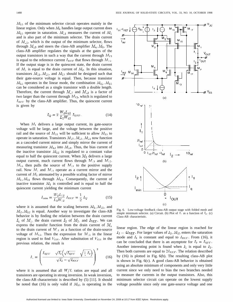
Because of the low number of components and the low cur-rent consumption, the class-AB control with simple minimum
selector has been selected to be applied in a complete op-ampimplementation, as shown in Fig. 7. The op-amp has a PMOSinput stage , allowing common-mode input voltagedown to the negative rail. The input stage drives a cascodingand summing circuit consisting of a current mirrorand cascodes The summing cir-cuit drives the output stage with class-AB control
The class-AB control uses the simple minimumselector , as discussed in Section III. Theminimum selector drives the class-AB amplifierusing transistor The class-AB amplifier is part of thefolded mesh Frequency compen-sation is obtained using Miller capacitors andThe Miller capacitors determine the unity-gain frequencyof the amplifier as given by
(19)
where is the transconductance of the input stage andis the total value of the Miller capacitors. The second pole isshifted to a frequency of
(20)
where is the transconductance of the output stage,is the gate-source capacitance of the output stage includingall parasitics connected to the gates, and is the loadcapacitance including all parasitic capacitance connected tothe output. The phase margin is given by
(21)With of 1.4 pF, of 8 pF, of 2 pF, and
of 1 mA/V, the second pole is shifted to 10 MHz. To achieve
Authorized licensed use limited to: Iowa State University. Downloaded on November 24, 2008 at 10:17 from IEEE Xplore. Restrictions apply.
1490 IEEE JOURNAL OF SOLID-STATE CIRCUITS, VOL. 33, NO. 10, OCTOBER 1998
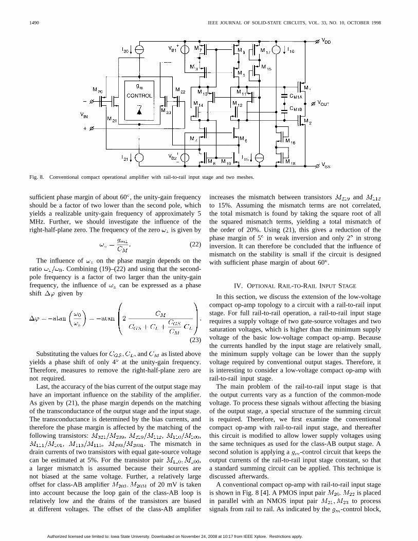
Fig. 8. Conventional compact operational amplifier with rail-to-rail input stage and two meshes.
sufficient phase margin of about 60, the unity-gain frequencyshould be a factor of two lower than the second pole, whichyields a realizable unity-gain frequency of approximately 5MHz. Further, we should investigate the influence of theright-half-plane zero. The frequency of the zerois given by
(22)
The influence of on the phase margin depends on theratio Combining (19)–(22) and using that the second-pole frequency is a factor of two larger than the unity-gainfrequency, the influence of can be expressed as a phaseshift given by
(23)
Substituting the values for and as listed aboveyields a phase shift of only 4at the unity-gain frequency.Therefore, measures to remove the right-half-plane zero arenot required.
Last, the accuracy of the bias current of the output stage mayhave an important influence on the stability of the amplifier.As given by (21), the phase margin depends on the matchingof the transconductance of the output stage and the input stage.The transconductance is determined by the bias currents, andtherefore the phase margin is affected by the matching of thefollowing transistors: , , ,
, , . The mismatch indrain currents of two transistors with equal gate-source voltagecan be estimated at 5%. For the transistor pair ,a larger mismatch is assumed because their sources arenot biased at the same voltage. Further, a relatively largeoffset for class-AB amplifier of 20 mV is takeninto account because the loop gain of the class-AB loop isrelatively low and the drains of the transistors are biasedat different voltages. The offset of the class-AB amplifier
increases the mismatch between transistors andto 15%. Assuming the mismatch terms are not correlated,the total mismatch is found by taking the square root of allthe squared mismatch terms, yielding a total mismatch ofthe order of 20%. Using (21), this gives a reduction of thephase margin of 5 in weak inversion and only 2in stronginversion. It can therefore be concluded that the influence ofmismatch on the stability is small if the circuit is designedwith sufficient phase margin of about 60.
IV. OPTIONAL RAIL -TO-RAIL INPUT STAGE
In this section, we discuss the extension of the low-voltagecompact op-amp topology to a circuit with a rail-to-rail inputstage. For full rail-to-rail operation, a rail-to-rail input stagerequires a supply voltage of two gate-source voltages and twosaturation voltages, which is higher than the minimum supplyvoltage of the basic low-voltage compact op-amp. Becausethe currents handled by the input stage are relatively small,the minimum supply voltage can be lower than the supplyvoltage required by conventional output stages. Therefore, itis interesting to consider a low-voltage compact op-amp withrail-to-rail input stage.
The main problem of the rail-to-rail input stage is thatthe output currents vary as a function of the common-modevoltage. To process these signals without affecting the biasingof the output stage, a special structure of the summing circuitis required. Therefore, we first examine the conventionalcompact op-amp with rail-to-rail input stage, and thereafterthis circuit is modified to allow lower supply voltages usingthe same techniques as used for the class-AB output stage. Asecond solution is applying a -control circuit that keeps theoutput currents of the rail-to-rail input stage constant, so thata standard summing circuit can be applied. This technique isdiscussed afterwards.
A conventional compact op-amp with rail-to-rail input stageis shown in Fig. 8 [4]. A PMOS input pair is placedin parallel with an NMOS input pair to processsignals from rail to rail. As indicated by the -control block,
Authorized licensed use limited to: Iowa State University. Downloaded on November 24, 2008 at 10:17 from IEEE Xplore. Restrictions apply.
DE LANGEN AND HUIJSING: AMPLIFIER CELLS FOR VLSI 1491
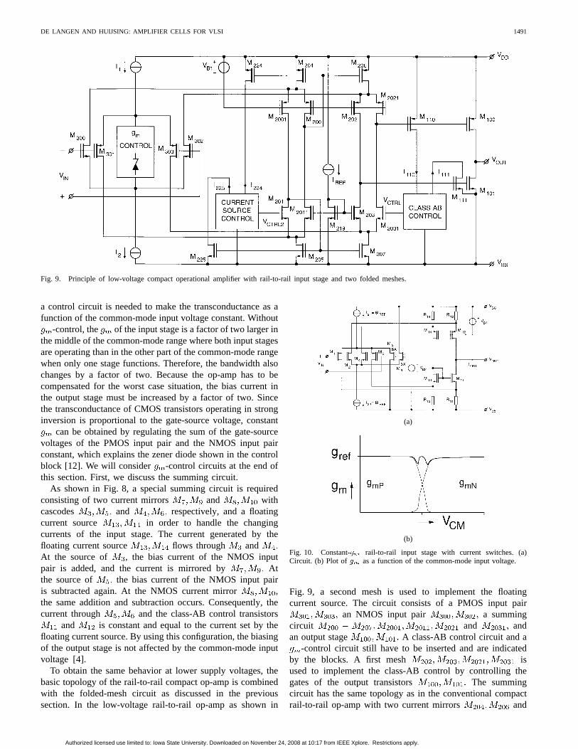
Fig. 9. Principle of low-voltage compact operational amplifier with rail-to-rail input stage and two folded meshes.
a control circuit is needed to make the transconductance as afunction of the common-mode input voltage constant. Without
-control, the of the input stage is a factor of two larger inthe middle of the common-mode range where both input stagesare operating than in the other part of the common-mode rangewhen only one stage functions. Therefore, the bandwidth alsochanges by a factor of two. Because the op-amp has to becompensated for the worst case situation, the bias current inthe output stage must be increased by a factor of two. Sincethe transconductance of CMOS transistors operating in stronginversion is proportional to the gate-source voltage, constant
can be obtained by regulating the sum of the gate-sourcevoltages of the PMOS input pair and the NMOS input pairconstant, which explains the zener diode shown in the controlblock [12]. We will consider -control circuits at the end ofthis section. First, we discuss the summing circuit.
As shown in Fig. 8, a special summing circuit is requiredconsisting of two current mirrors and withcascodes and respectively, and a floatingcurrent source in order to handle the changingcurrents of the input stage. The current generated by thefloating current source flows through andAt the source of , the bias current of the NMOS inputpair is added, and the current is mirrored by Atthe source of the bias current of the NMOS input pairis subtracted again. At the NMOS current mirror ,the same addition and subtraction occurs. Consequently, thecurrent through and the class-AB control transistors
and is constant and equal to the current set by thefloating current source. By using this configuration, the biasingof the output stage is not affected by the common-mode inputvoltage [4].
To obtain the same behavior at lower supply voltages, thebasic topology of the rail-to-rail compact op-amp is combinedwith the folded-mesh circuit as discussed in the previoussection. In the low-voltage rail-to-rail op-amp as shown in
(a)
(b)
Fig. 10. Constant-gm rail-to-rail input stage with current switches. (a)Circuit. (b) Plot ofgm as a function of the common-mode input voltage.
Fig. 9, a second mesh is used to implement the floatingcurrent source. The circuit consists of a PMOS input pair
an NMOS input pair a summingcircuit and andan output stage A class-AB control circuit and a
-control circuit still have to be inserted and are indicatedby the blocks. A first mesh isused to implement the class-AB control by controlling thegates of the output transistors The summingcircuit has the same topology as in the conventional compactrail-to-rail op-amp with two current mirrors and
Authorized licensed use limited to: Iowa State University. Downloaded on November 24, 2008 at 10:17 from IEEE Xplore. Restrictions apply.
1492 IEEE JOURNAL OF SOLID-STATE CIRCUITS, VOL. 33, NO. 10, OCTOBER 1998
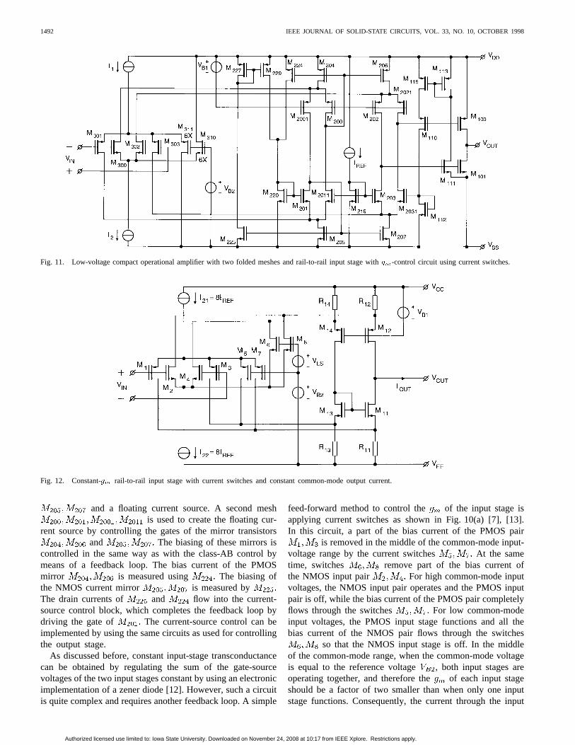
Fig. 11. Low-voltage compact operational amplifier with two folded meshes and rail-to-rail input stage withgm-control circuit using current switches.
Fig. 12. Constant-gm rail-to-rail input stage with current switches and constant common-mode output current.
and a floating current source. A second meshis used to create the floating cur-
rent source by controlling the gates of the mirror transistorsand The biasing of these mirrors is
controlled in the same way as with the class-AB control bymeans of a feedback loop. The bias current of the PMOSmirror is measured using The biasing ofthe NMOS current mirror is measured byThe drain currents of and flow into the current-source control block, which completes the feedback loop bydriving the gate of The current-source control can beimplemented by using the same circuits as used for controllingthe output stage.
As discussed before, constant input-stage transconductancecan be obtained by regulating the sum of the gate-sourcevoltages of the two input stages constant by using an electronicimplementation of a zener diode [12]. However, such a circuitis quite complex and requires another feedback loop. A simple
feed-forward method to control the of the input stage isapplying current switches as shown in Fig. 10(a) [7], [13].In this circuit, a part of the bias current of the PMOS pair
is removed in the middle of the common-mode input-voltage range by the current switches At the sametime, switches remove part of the bias current ofthe NMOS input pair For high common-mode inputvoltages, the NMOS input pair operates and the PMOS inputpair is off, while the bias current of the PMOS pair completelyflows through the switches For low common-modeinput voltages, the PMOS input stage functions and all thebias current of the NMOS pair flows through the switches
so that the NMOS input stage is off. In the middleof the common-mode range, when the common-mode voltageis equal to the reference voltage , both input stages areoperating together, and therefore the of each input stageshould be a factor of two smaller than when only one inputstage functions. Consequently, the current through the input
Authorized licensed use limited to: Iowa State University. Downloaded on November 24, 2008 at 10:17 from IEEE Xplore. Restrictions apply.
DE LANGEN AND HUIJSING: AMPLIFIER CELLS FOR VLSI 1493
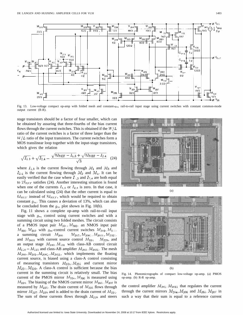
Fig. 13. Low-voltage compact op-amp with folded mesh and constant-gm rail-to-rail input stage using current switches with constant common-modeoutput current (R-R).
stage transistors should be a factor of four smaller, which canbe obtained by assuring that three-fourths of the bias currentflows through the current switches. This is obtained if theratio of the current switches is a factor of three larger than the
ratio of the input transistors. The current switches form aMOS translinear loop together with the input-stage transistors,which gives the relation
(24)
where is the current flowing through and andis the current flowing through and It can be
easily verified that the case where and are both equalto satisfies (24). Another interesting situation is foundwhen one of the currents or is zero. In that case, itcan be calculated using (24) that the other current is equal to
instead of , which would be required to obtainconstant This causes a deviation of 13%, which can alsobe concluded from the plot shown in Fig. 10(b).
Fig. 11 shows a complete op-amp with rail-to-rail inputstage with control using current switches and with asumming circuit using two folded meshes. The circuit consistsof a PMOS input pair an NMOS input pair
with -control current switchesa summing circuitand with current source control , andan output stage with class-AB control circuit
and class-AB amplifier The mesh, which implements the floating
current source, is biased using a class-A control consistingof measuring transistors and current mirror
A class-A control is sufficient because the biascurrent in the summing circuit is relatively small. The biascurrent of the PMOS mirror is measured using
The biasing of the NMOS current mirror ismeasured by The drain current of flows throughmirror and is added to the drain current ofThe sum of these currents flows through and steers
(a)
(b)
Fig. 14. Photomicrographs of compact low-voltage op-amp. (a) PMOSop-amp. (b) R-R op-amp.
the control amplifier that regulates the currentthrough the current mirrors and insuch a way that their sum is equal to a reference current
Authorized licensed use limited to: Iowa State University. Downloaded on November 24, 2008 at 10:17 from IEEE Xplore. Restrictions apply.
1494 IEEE JOURNAL OF SOLID-STATE CIRCUITS, VOL. 33, NO. 10, OCTOBER 1998
(a)
(b)
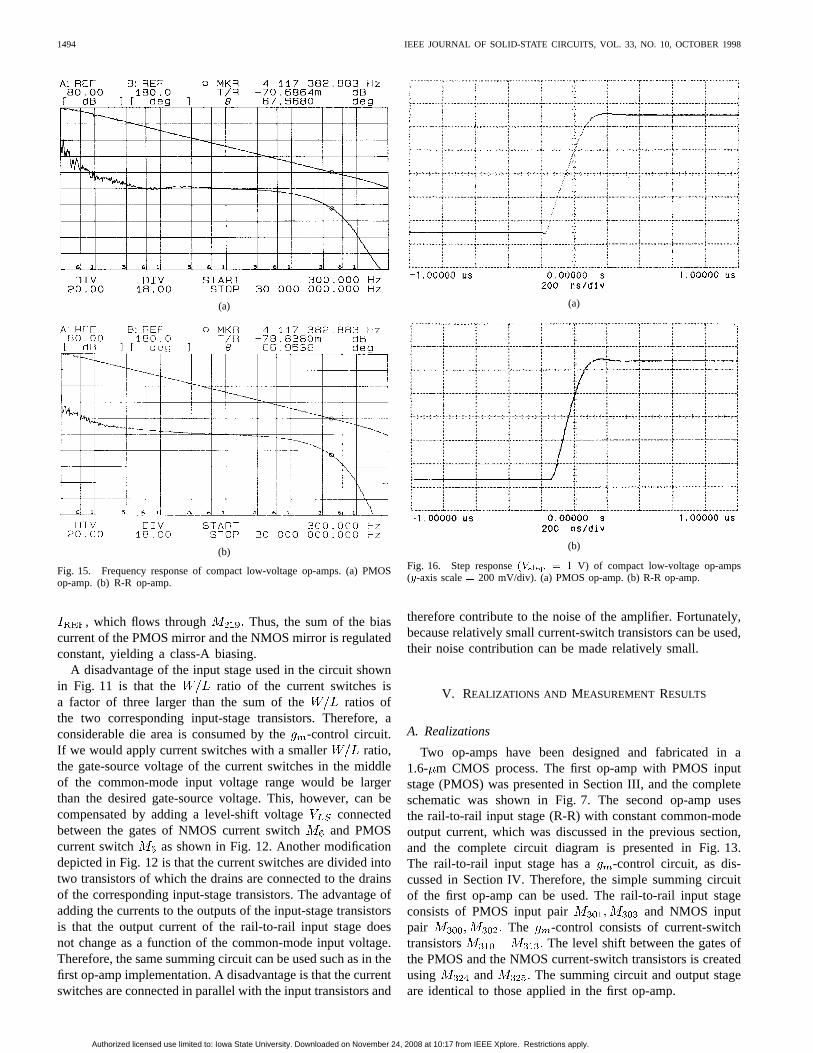
Fig. 15. Frequency response of compact low-voltage op-amps. (a) PMOSop-amp. (b) R-R op-amp.
, which flows through Thus, the sum of the biascurrent of the PMOS mirror and the NMOS mirror is regulatedconstant, yielding a class-A biasing.
A disadvantage of the input stage used in the circuit shownin Fig. 11 is that the ratio of the current switches isa factor of three larger than the sum of the ratios ofthe two corresponding input-stage transistors. Therefore, aconsiderable die area is consumed by the-control circuit.If we would apply current switches with a smaller ratio,the gate-source voltage of the current switches in the middleof the common-mode input voltage range would be largerthan the desired gate-source voltage. This, however, can becompensated by adding a level-shift voltage connectedbetween the gates of NMOS current switch and PMOScurrent switch as shown in Fig. 12. Another modificationdepicted in Fig. 12 is that the current switches are divided intotwo transistors of which the drains are connected to the drainsof the corresponding input-stage transistors. The advantage ofadding the currents to the outputs of the input-stage transistorsis that the output current of the rail-to-rail input stage doesnot change as a function of the common-mode input voltage.Therefore, the same summing circuit can be used such as in thefirst op-amp implementation. A disadvantage is that the currentswitches are connected in parallel with the input transistors and
(a)
(b)
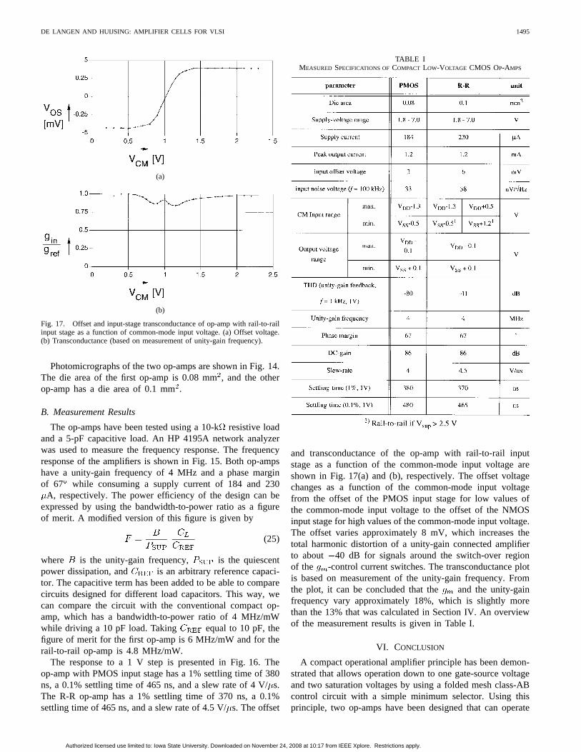
Fig. 16. Step response(Vstep = 1 V) of compact low-voltage op-amps(y-axis scale= 200 mV/div). (a) PMOS op-amp. (b) R-R op-amp.
therefore contribute to the noise of the amplifier. Fortunately,because relatively small current-switch transistors can be used,their noise contribution can be made relatively small.
V. REALIZATIONS AND MEASUREMENT RESULTS
A. Realizations
Two op-amps have been designed and fabricated in a1.6- m CMOS process. The first op-amp with PMOS inputstage (PMOS) was presented in Section III, and the completeschematic was shown in Fig. 7. The second op-amp usesthe rail-to-rail input stage (R-R) with constant common-modeoutput current, which was discussed in the previous section,and the complete circuit diagram is presented in Fig. 13.The rail-to-rail input stage has a -control circuit, as dis-cussed in Section IV. Therefore, the simple summing circuitof the first op-amp can be used. The rail-to-rail input stageconsists of PMOS input pair and NMOS inputpair The -control consists of current-switchtransistors The level shift between the gates ofthe PMOS and the NMOS current-switch transistors is createdusing and The summing circuit and output stageare identical to those applied in the first op-amp.
Authorized licensed use limited to: Iowa State University. Downloaded on November 24, 2008 at 10:17 from IEEE Xplore. Restrictions apply.
DE LANGEN AND HUIJSING: AMPLIFIER CELLS FOR VLSI 1495
(a)
(b)
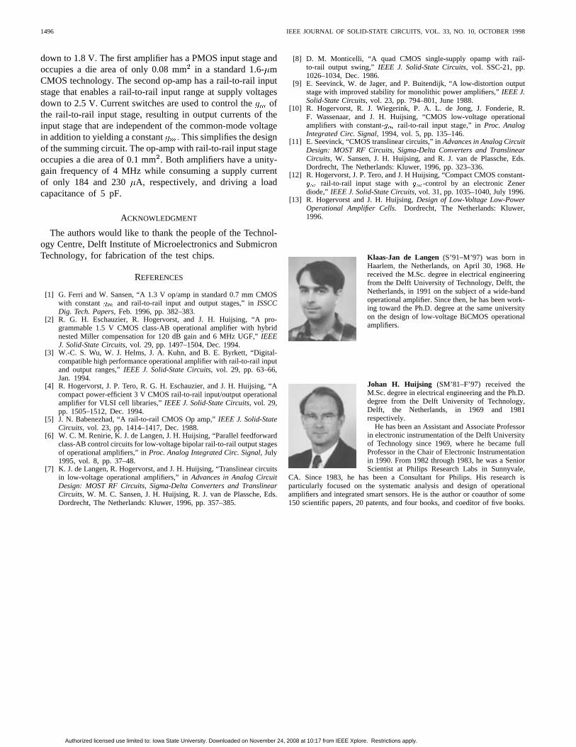
Fig. 17. Offset and input-stage transconductance of op-amp with rail-to-railinput stage as a function of common-mode input voltage. (a) Offset voltage.(b) Transconductance (based on measurement of unity-gain frequency).
Photomicrographs of the two op-amps are shown in Fig. 14.The die area of the first op-amp is 0.08 mm, and the otherop-amp has a die area of 0.1 mm.
B. Measurement Results
The op-amps have been tested using a 10-kresistive loadand a 5-pF capacitive load. An HP 4195A network analyzerwas used to measure the frequency response. The frequencyresponse of the amplifiers is shown in Fig. 15. Both op-ampshave a unity-gain frequency of 4 MHz and a phase marginof 67 while consuming a supply current of 184 and 230
A, respectively. The power efficiency of the design can beexpressed by using the bandwidth-to-power ratio as a figureof merit. A modified version of this figure is given by
(25)
where is the unity-gain frequency, is the quiescentpower dissipation, and is an arbitrary reference capaci-tor. The capacitive term has been added to be able to comparecircuits designed for different load capacitors. This way, wecan compare the circuit with the conventional compact op-amp, which has a bandwidth-to-power ratio of 4 MHz/mWwhile driving a 10 pF load. Taking equal to 10 pF, thefigure of merit for the first op-amp is 6 MHz/mW and for therail-to-rail op-amp is 4.8 MHz/mW.
The response to a 1 V step is presented in Fig. 16. Theop-amp with PMOS input stage has a 1% settling time of 380ns, a 0.1% settling time of 465 ns, and a slew rate of 4 V/s.The R-R op-amp has a 1% settling time of 370 ns, a 0.1%settling time of 465 ns, and a slew rate of 4.5 V/s. The offset
TABLE IMEASURED SPECIFICATIONS OFCOMPACT LOW-VOLTAGE CMOS OP-AMPS
and transconductance of the op-amp with rail-to-rail inputstage as a function of the common-mode input voltage areshown in Fig. 17(a) and (b), respectively. The offset voltagechanges as a function of the common-mode input voltagefrom the offset of the PMOS input stage for low values ofthe common-mode input voltage to the offset of the NMOSinput stage for high values of the common-mode input voltage.The offset varies approximately 8 mV, which increases thetotal harmonic distortion of a unity-gain connected amplifierto about 40 dB for signals around the switch-over regionof the -control current switches. The transconductance plotis based on measurement of the unity-gain frequency. Fromthe plot, it can be concluded that the and the unity-gainfrequency vary approximately 18%, which is slightly morethan the 13% that was calculated in Section IV. An overviewof the measurement results is given in Table I.
VI. CONCLUSION
A compact operational amplifier principle has been demon-strated that allows operation down to one gate-source voltageand two saturation voltages by using a folded mesh class-ABcontrol circuit with a simple minimum selector. Using thisprinciple, two op-amps have been designed that can operate
Authorized licensed use limited to: Iowa State University. Downloaded on November 24, 2008 at 10:17 from IEEE Xplore. Restrictions apply.
1496 IEEE JOURNAL OF SOLID-STATE CIRCUITS, VOL. 33, NO. 10, OCTOBER 1998
down to 1.8 V. The first amplifier has a PMOS input stage andoccupies a die area of only 0.08 mmin a standard 1.6-mCMOS technology. The second op-amp has a rail-to-rail inputstage that enables a rail-to-rail input range at supply voltagesdown to 2.5 V. Current switches are used to control theofthe rail-to-rail input stage, resulting in output currents of theinput stage that are independent of the common-mode voltagein addition to yielding a constant This simplifies the designof the summing circuit. The op-amp with rail-to-rail input stageoccupies a die area of 0.1 mmBoth amplifiers have a unity-gain frequency of 4 MHz while consuming a supply currentof only 184 and 230 A, respectively, and driving a loadcapacitance of 5 pF.
ACKNOWLEDGMENT
The authors would like to thank the people of the Technol-ogy Centre, Delft Institute of Microelectronics and SubmicronTechnology, for fabrication of the test chips.
REFERENCES
[1] G. Ferri and W. Sansen, “A 1.3 V op/amp in standard 0.7 mm CMOSwith constantgm and rail-to-rail input and output stages,” inISSCCDig. Tech. Papers, Feb. 1996, pp. 382–383.
[2] R. G. H. Eschauzier, R. Hogervorst, and J. H. Huijsing, “A pro-grammable 1.5 V CMOS class-AB operational amplifier with hybridnested Miller compensation for 120 dB gain and 6 MHz UGF,”IEEEJ. Solid-State Circuits, vol. 29, pp. 1497–1504, Dec. 1994.
[3] W.-C. S. Wu, W. J. Helms, J. A. Kuhn, and B. E. Byrkett, “Digital-compatible high performance operational amplifier with rail-to-rail inputand output ranges,”IEEE J. Solid-State Circuits, vol. 29, pp. 63–66,Jan. 1994.
[4] R. Hogervorst, J. P. Tero, R. G. H. Eschauzier, and J. H. Huijsing, “Acompact power-efficient 3 V CMOS rail-to-rail input/output operationalamplifier for VLSI cell libraries,”IEEE J. Solid-State Circuits, vol. 29,pp. 1505–1512, Dec. 1994.
[5] J. N. Babenezhad, “A rail-to-rail CMOS Op amp,”IEEE J. Solid-StateCircuits, vol. 23, pp. 1414–1417, Dec. 1988.
[6] W. C. M. Renirie, K. J. de Langen, J. H. Huijsing, “Parallel feedforwardclass-AB control circuits for low-voltage bipolar rail-to-rail output stagesof operational amplifiers,” inProc. Analog Integrated Circ. Signal, July1995, vol. 8, pp. 37–48.
[7] K. J. de Langen, R. Hogervorst, and J. H. Huijsing, “Translinear circuitsin low-voltage operational amplifiers,” inAdvances in Analog CircuitDesign: MOST RF Circuits, Sigma-Delta Converters and TranslinearCircuits, W. M. C. Sansen, J. H. Huijsing, R. J. van de Plassche, Eds.Dordrecht, The Netherlands: Kluwer, 1996, pp. 357–385.
[8] D. M. Monticelli, “A quad CMOS single-supply opamp with rail-to-rail output swing,” IEEE J. Solid-State Circuits, vol. SSC-21, pp.1026–1034, Dec. 1986.
[9] E. Seevinck, W. de Jager, and P. Buitendijk, “A low-distortion outputstage with improved stability for monolithic power amplifiers,”IEEE J.Solid-State Circuits, vol. 23, pp. 794–801, June 1988.
[10] R. Hogervorst, R. J. Wiegerink, P. A. L. de Jong, J. Fonderie, R.F. Wassenaar, and J. H. Huijsing, “CMOS low-voltage operationalamplifiers with constant-gm rail-to-rail input stage,” inProc. AnalogIntegrated Circ. Signal, 1994, vol. 5, pp. 135–146.
[11] E. Seevinck, “CMOS translinear circuits,” inAdvances in Analog CircuitDesign: MOST RF Circuits, Sigma-Delta Converters and TranslinearCircuits, W. Sansen, J. H. Huijsing, and R. J. van de Plassche, Eds.Dordrecht, The Netherlands: Kluwer, 1996, pp. 323–336.
[12] R. Hogervorst, J. P. Tero, and J. H Huijsing, “Compact CMOS constant-gm rail-to-rail input stage withgm-control by an electronic Zenerdiode,” IEEE J. Solid-State Circuits, vol. 31, pp. 1035–1040, July 1996.
[13] R. Hogervorst and J. H. Huijsing,Design of Low-Voltage Low-PowerOperational Amplifier Cells. Dordrecht, The Netherlands: Kluwer,1996.
Klaas-Jan de Langen (S’91–M’97) was born inHaarlem, the Netherlands, on April 30, 1968. Hereceived the M.Sc. degree in electrical engineeringfrom the Delft University of Technology, Delft, theNetherlands, in 1991 on the subject of a wide-bandoperational amplifier. Since then, he has been work-ing toward the Ph.D. degree at the same universityon the design of low-voltage BiCMOS operationalamplifiers.
Johan H. Huijsing (SM’81–F’97) received theM.Sc. degree in electrical engineering and the Ph.D.degree from the Delft University of Technology,Delft, the Netherlands, in 1969 and 1981respectively.
He has been an Assistant and Associate Professorin electronic instrumentation of the Delft Universityof Technology since 1969, where he became fullProfessor in the Chair of Electronic Instrumentationin 1990. From 1982 through 1983, he was a SeniorScientist at Philips Research Labs in Sunnyvale,
CA. Since 1983, he has been a Consultant for Philips. His research isparticularly focused on the systematic analysis and design of operationalamplifiers and integrated smart sensors. He is the author or coauthor of some150 scientific papers, 20 patents, and four books, and coeditor of five books.
Authorized licensed use limited to: Iowa State University. Downloaded on November 24, 2008 at 10:17 from IEEE Xplore. Restrictions apply.