Embed Size (px)
Citation preview

University of South CarolinaScholar Commons
Theses and Dissertations
6-30-2016
Comparative Analysis Of Current ControlMethods For Modular Multilevel ConvertersJordan D. RogersUniversity of South Carolina
Follow this and additional works at: https://scholarcommons.sc.edu/etd
Part of the Electrical and Computer Engineering Commons
This Open Access Thesis is brought to you by Scholar Commons. It has been accepted for inclusion in Theses and Dissertations by an authorizedadministrator of Scholar Commons. For more information, please contact [email protected].
Recommended CitationRogers, J. D.(2016). Comparative Analysis Of Current Control Methods For Modular Multilevel Converters. (Master's thesis). Retrievedfrom https://scholarcommons.sc.edu/etd/3419

COMPARATIVE ANALYSIS OF CURRENT CONTROL METHODS FOR MODULAR
MULTILEVEL CONVERTERS
by
Jordan D. Rogers
Bachelor of Science
University of South Carolina, 2013
Submitted in Partial Fulfillment of the Requirements
For the Degree of Master of Science in
Electrical Engineering
College of Engineering and Computing
University of South Carolina
2016
Accepted by:
Herbert Ginn III, Director of Thesis
Andrea Benigni, Reader
Lacy Ford, Senior Vice Provost and Dean of Graduate Studies

ii
© Copyright by Jordan D. Rogers, 2016
All Rights Reserved.

iii
ACKNOWLEDGEMENTS
I want to thank the EE Department faculty at the University of South Carolina for
helping me get to this point. I gained an invaluable amount of knowledge and experience
during my entire tenure, and I am grateful for this stepping stone for my future successes.
I would also like to thank Dr. Herbert Ginn for the opportunity to work with him on this
project and for his support and guidance throughout my graduate school tenure. Lastly, I
would like to give a special thanks to Mitch Thompkins, David Metts and Jonathan
Siegers for their invaluable friendship and support in both technical matters as well as
personal.

iv
ABSTRACT
Modular Multilevel Converters (MMCs) are power electronic converters
comprised of a series connection of sub-modules. Their modular structure allows for the
possibility to design high-voltage converters that are suitable for utility applications due
to the modular fail-safe structure with reduced switching frequency requirements. Some
areas of interesting research specific to the MMC topology include modulation
techniques, control methods, capacitor voltage balancing strategies, and circulating
current suppression control. This thesis presents the development of a predictive current
control for MMCs that has the benefit of inherently reduced circulating currents within
the converter’s phase units. Two other typical MMC current control strategies are
implemented for comparison with the predictive current control.
The operation and modeling, multi-loop control design, and digital simulation of a
MMC are presented using MATLAB/Simulink software. An effective control scheme is
implemented using a cascade control approach, with an outer power controller and an
inner current controller. The outer loop is implemented with a conventional synchronous
proportional-integral (PI) controller. The inner loop is then implemented with PI,
proportional resonant (PR), and predictive controllers and the controller error signal
dynamics for each method are observed. The predictive arm-current controller is shown
to have significantly reduced circulating currents in the phase units, which reduces arm
current distortion and submodule capacitor voltage ripple.

v
TABLE OF CONTENTS
ACKNOWLEDGEMENTS ........................................................................................................ iii
ABSTRACT .......................................................................................................................... iv
LIST OF TABLES ................................................................................................................. vii
LIST OF FIGURES ............................................................................................................... viii
LIST OF ABBREVIATIONS ..................................................................................................... xi
CHAPTER 1 MODULAR MULTILEVEL CONVERTERS ............................................................. 1
1.1 INTRODUCTION ........................................................................................................... 1
1.2 MMC TOPOLOGY ....................................................................................................... 2
1.3 PRINCIPLE OF OPERATION .......................................................................................... 5
1.4 MODULATION TECHNIQUES ........................................................................................ 7
1.5 CAPACITOR VOLTAGE BALANCING .......................................................................... 11
CHAPTER 2 CONTROL STRATEGIES AND TUNING ............................................................... 14
2.1 BACKGROUND .......................................................................................................... 16
2.2 SYNCHRONOUS PI CONTROLLER .............................................................................. 22
2.3 PROPORTIONAL RESONANT CONTROLLER ................................................................ 31
2.4 PREDICTIVE CONTROLLER ........................................................................................ 37
CHAPTER 3 SIMULATION RESULTS AND COMPARISON ....................................................... 41
3.1 PI CONTROL SIMULATION ........................................................................................ 43

vi
3.2 PR CONTROL SIMULATION ....................................................................................... 49
3.3 PREDICTIVE CONTROL SIMULATION ......................................................................... 54
3.4 TOTAL HARMONIC DISTORTION ............................................................................... 66
CHAPTER 4 CONCLUSION ................................................................................................... 68
REFERENCES ...................................................................................................................... 70
APPENDIX A – MEASURMENT SCHEMATIC......................................................................... 72

vii
LIST OF TABLES
Table 3.1 MMC System Parameters ..................................................................................41
Table 3.2 THD Measurements ...........................................................................................67

viii
LIST OF FIGURES
Figure 1.1 Modular multilevel converter arm ......................................................................2
Figure 1.2 Modular multilevel converter topology ..............................................................3
Figure 1.3 MMC Submodule ...............................................................................................4
Figure 1.4 Three-phase MMC equivalent circuit .................................................................5
Figure 1.5 Sinusoidal PWM generation ...............................................................................8
Figure 1.6 20 submodule PSC-PWM.................................................................................10
Figure 1.7 PSC-PWM Reference waveform ......................................................................10
Figure 1.8 Capacitor voltage balancing algorithm .............................................................12
Figure 2.1 Current mode control loop................................................................................14
Figure 2.2 MMC control diagram ......................................................................................16
Figure 2.3 Phase leg equivalent circuit ..............................................................................17
Figure 2.4 Power regulator block diagram ........................................................................19
Figure 2.5 Simplified primary control loop .......................................................................20
Figure 2.6 Decoupled 𝑑𝑞-frame PI controller ...................................................................22
Figure 2.7 Technical optimum PI controller open-loop margin plot .................................25
Figure 2.8 Technical optimum PI controller closed-loop Bode plot .................................26
Figure 2.9 PI closed-loop response comparison ................................................................27
Figure 2.10 PI control step response comparison ..............................................................28
Figure 2.11 Alternative PI controller open-loop margin plot ............................................29
Figure 2.12 Alternative PI controller closed-loop Bode plot .............................................30

ix
Figure 2.13 Alternative PI control step response comparison ...........................................31
Figure 2.14 PR outer power and inner current control diagrams .......................................32
Figure 2.15 PR coefficients comparison ............................................................................33
Figure 2.16 Technical optimum PR controller open-loop margin plot ..............................35
Figure 2.17 Technical optimum PR closed-loop Bode plot ...............................................36
Figure 2.18 Upper and lower arm deadbeat control equivalent circuits ............................39
Figure 3.1 PI controller Simulink model ...........................................................................43
Figure 3.2 PI controller simulation step response ..............................................................43
Figure 3.3 PI controller simulation step response (prefiltered) .........................................44
Figure 3.4 PI controller AC and DC power transient ........................................................45
Figure 3.5 Phase 𝑎 current tracking under PI control ........................................................46
Figure 3.6 PI control phase current error ...........................................................................46
Figure 3.7 PI control circulating currents ..........................................................................47
Figure 3.8 PI control circulating currents (zoomed) ..........................................................48
Figure 3.9 MMC AC-side voltages under PI control .........................................................48
Figure 3.10 PR controller Simulink model ........................................................................49
Figure 3.11 PR controller simulation step response ..........................................................50
Figure 3.12 PR control AC and DC power transient .........................................................51
Figure 3.13 Phase 𝑎 current tracking under PR control .....................................................51
Figure 3.14 PR control simulation error ............................................................................52
Figure 3.15 PR control circulating currents .......................................................................53
Figure 3.16 PR control circulating currents (zoomed).......................................................53
Figure 3.17 MMC AC-side voltages under PR control .....................................................54

x
Figure 3.18 Phase 𝑎 predictive Simulink model ................................................................55
Figure 3.19 Predictive controller Simulink model .............................................................56
Figure 3.20 Predictive controller simulation step response ...............................................57
Figure 3.21 Predictive control AC and DC power transient ..............................................58
Figure 3.22 Arm current tracking under predictive control ...............................................59
Figure 3.23 Predictive controller arm current error ...........................................................59
Figure 3.24 Phase 𝑎 current tracking under predictive control..........................................60
Figure 3.25 Predictive control simulation phase current error ..........................................61
Figure 3.26 DC-bus to ground variation measurement ......................................................62
Figure 3.27 Zoomed in phase current error vs. 𝑉𝑝𝑑𝑐−𝑔 measurement ...............................63
Figure 3.28 Predictive control circulating currents............................................................64
Figure 3.29 Predictive control circulating currents (zoomed) ...........................................65
Figure 3.30 MMC AC-side voltages under predictive control ..........................................66
Figure A.1 DC-bus voltage variation measurement locations ...........................................72

xi
LIST OF ABBREVIATIONS
HVDC ........................................................................................ High voltage direct current
IGBT ................................................................................. Insulated-gate Bipolar Transistor
MMC ..................................................................................... Modular Multilevel Converter
PD-PWM............................................................Phase-disposition Pulse-width Modulation
PI .......................................................................................................... Proportional Integral
PR ....................................................................................................... Proportional Resonant
PSC-PWM.................................................... Phase-shifted Carrier Pulse-width Modulation
SVM ............................................................................................. Space Vector Modulation
VSC .............................................................................................. Voltage-source Converter
1
CHAPTER 1
MODULAR MULTILEVEL CONVERTERS
1.1 INTRODUCTION
The modular multilevel converter (MMC) was first proposed for high voltage
applications by Dr. Lescinar in [1]. The MMC is a three-phase converter composed of
low voltage semiconductor valves that can be manipulated to behave like controlled
voltage sources in medium and high voltage applications. The MMC is a scalable
technology with many advantages over more conventional two and three level voltage
source converters (VSCs). Its modular topology allows for scalability of medium to high
voltage ranges, as well as for control of harmonic distortion by varying the number of
submodules used in the design. This converter topology also allows for lower switching
frequency requirements, which significantly decreases the converter’s switching losses.
Modular multilevel converters are also suitable for use in interfacing renewable energy
power sources to the conventional AC grid.
This thesis will focus on the MMC topology described below and will specifically
investigate three different digital current control techniques. The different approaches for
digital current control have a significant effect on the converter’s operation such as its
transient response, capacitor voltage ripple, circulating current magnitude, and harmonic
distortion of the output waveforms. Specifically, this thesis investigates two conventional
strategies and a third novel approach and demonstrates the advantage of inherent

2
circulating current suppression with the third strategy. The techniques used in the design
of each of the controllers are described in detail, and then the implementations and
simulated results follow.
1.2 MMC TOPOLOGY
The converter is composed of six arms, two per phase, that are each connected to
one AC terminal and one DC terminal. The structure of each arm is composed of N
series-connected submodules and a current limiting inductor, 𝐿𝑜, as shown in Figure 1.1.
SM1
SM2
SMN
Lo
arm
N sub-
modules
Figure 1.1 Modular multilevel converter arm
Each phase leg of the converter, or phase unit, is composed of an upper and a
lower arm. Each phase unit is attached to the AC terminal between the two arm inductors
and to the DC terminals at the opposite ends of the arms. The structure of a three-phase
MMC is shown in Figure 1.2.

3
SM1
SM2
SMN
Lo
SM1
SM2
SMN
Lo
SM1
SM2
SMN
Lo
Lo Lo Lo
SM1
SM2
SMN
SM1
SM2
SMN
SM1
SM2
SMN
Lvsa
vsb
vsc
Vdc
va
vbvc
Figure 1.2 Modular multilevel converter topology
Each submodule consists of two controllable semiconductor switches and a
storage capacitor, 𝐶𝑜. In this case, the switches are insulated-gate bipolar transistors
(IGBTs). The submodule structure is shown in Figure 1.3 and the two switches are
complimentary, such that 𝐶𝑜 is either connected in the arm or bypassed.

4
Co
+
Figure 1.3 MMC Submodule
While the upper switch is conducting and the lower is not, the capacitor is inserted into
the arm with a nominal voltage 𝑉𝑑𝑐/𝑁 . Then, while the lower switch is conducting and
the upper is not, the storage capacitor is bypassed. The freewheeling diodes allow for
reverse current flow when the current through the submodule is negative.
Each arm voltage is controlled by inserting and bypassing the appropriate number
of submodules to produce the desired voltage waveform at the terminals. The control of
each submodule’s conduction state allows for the total arm voltage to be controlled
independently to N+1 discrete voltage levels. Zero volts is included as a level; thus, the
MMC naming convention is that of an (N+1)-level converter. If a higher number of
submodules is used, a higher quality voltage waveform can be produced because of the
ability to adjust the output by smaller voltage increments; however, the increase of
submodules adds control complexity, increased computational power requirements, and
higher switching device losses. The most significant driving factor for selecting the
appropriate level of an MMC is the voltage level required in the application for which it
will be utilized.

5
1.3 PRINCIPLE OF OPERATION
The three-phase equivalent circuit of an idealized MMC is shown in Figure 1.4,
where the submodules in each converter arm are represented by a controlled voltage
source. Each of the DC busses are connected to each end of two series-connected DC
sources denoted 𝑉𝑑𝑐+ and 𝑉𝑑𝑐
− .
vsa
vsb
vsc
L
Vpa Vpb Vpc
Vdc-
+
_
Vna Vnb Vnc
Ipa Ipb Ipc
Ina Inb Inc
+ + +
+ + +
ij
Idc
va
vb
vc
Vdc+
+
_
Figure 1.4 Three-phase MMC equivalent circuit
Vdc+
and Vdc- can be approximated by (1), where 𝑉𝑑𝑐 is the total DC bus voltage. The line
inductors, 𝐿, are considered to be very small, such that 𝑣𝑠𝑎 ≈ 𝑣𝑎. By applying KVL to the
equivalent circuit, the equations for the arm voltages can be shown by (2) and (3). 𝑉𝑝𝑗
and 𝑉𝑛𝑗 denote the arm voltages, where 𝑗 denotes the phase a, b, or c and 𝑝 and 𝑛

6
represent the positive and negative arm in the phase unit, respectively. Making the
assumption that the arm inductor value is very small, which is often true, the arm
inductor’s voltage can be ignored. Substituting (2) into (3), (4) can be obtained.
𝑉𝑑𝑐+ = 𝑉𝑑𝑐
− =𝑉𝑑𝑐
2 (1)
𝑉𝑝𝑗 =𝑉𝑑𝑐
2− 𝑣𝑗 (2)
𝑉𝑛𝑗 =𝑉𝑑𝑐
2+ 𝑣𝑗 (3)
𝑣𝑗 =(𝑉𝑛𝑗 − 𝑉𝑝𝑗)
2 (4)
The phase currents and arm currents can be defined by (5)-(7), and the circulating current
for each phase, 𝑖𝑐𝑖𝑟𝑗, by (8), where 𝑗 denotes phase a, b, or c.
𝑖𝑗 = 𝐼𝑛𝑗 − 𝐼𝑝𝑗 (5)
𝐼𝑝𝑗 = 𝑖𝑐𝑖𝑟𝑗 +𝑖𝑗
2 (6)
𝐼𝑛𝑗 = 𝑖𝑐𝑖𝑟𝑗 −𝑖𝑗
2 (7)
𝑖𝑐𝑖𝑟𝑗 =(𝐼𝑝𝑗 + 𝐼𝑛𝑗)
2 (8)
It is important to note that the description of the different operational sections of
an MMC will vary between “upper and lower” and “positive and negative.” It should be
clarified that the descriptions of “upper” and “positive” refer to the same section of the
converter, which contains the arms connected to the positive side of the DC bus, 𝑉𝑑𝑐+ .
Similarly, “lower” and “negative” both describe the arms connected to the negative side
of the DC bus, 𝑉𝑑𝑐− .

7
The circulating current, 𝑖𝑐𝑖𝑟𝑗, is a continuously flowing current present in all six
arms that is responsible for the power transmission of the converter, and does not affect
the AC-side voltages and currents. The undesirable circulating currents in an MMC are
due to voltage differences between each of the phase units, and are superimposed onto
the DC current flowing through each of the phase units [2]-[4]. The DC component in
each arm is quantified by the division of the total DC current by the number of phase
units. The AC components oscillate with twice the fundamental frequency and are
negative-sequence [21]. The equation for the total circulating current is defined by (9).
𝑖𝑐𝑖𝑟𝑗 =𝐼𝑑𝑐
3+ 𝑖2𝑓𝑗 (9)
Here, 𝑖𝑐𝑖𝑟𝑗 is the circulating current in each phase, 𝐼𝑑𝑐 is the total DC current present in
the converter, and 𝑖2𝑓𝑗 is the unwanted AC current circulating between the phase units at
twice the fundamental frequency.
1.4 MODULATION TECHNIQUES
The number of submodules required to be on or off in each of the converter’s
arms is driven by the modulation scheme. The modulator enforces the desired state of the
complementary gates in each of the submodules, resulting in the average arm voltage
needed for that time step. Pulse-width modulation (PWM) techniques are commonly used
in power electronic converters to achieve frequency and voltage variability. There are a
variety of techniques that can be used in the creation of PWM control signals, which can
allow for the reduction of harmonic distortion in the output waveforms and increased
modulation indexes, depending on the application.

8
Conventional pulse-width modulation uses one carrier waveform and one
reference waveform to generate a gate-driving signal. The carrier is some cyclical
waveform, typically either sawtooth or triangular, that is used as a comparison to the
reference. For example, when the reference is higher than the carrier, the PWM output is
high and when the reference becomes lower than the carrier, the PWM output transitions
to a low state. Of course, this convention can easily be reversed. Figure 1.5 shows a
single update sinusoidal reference PWM example, where Pulse 1 and Pulse 2 demonstrate
the two conventions and the so-called reference signal is labeled as “Internal generation
signal.”
Figure 1.5 Sinusoidal PWM generation [5]
This configuration is suitable for the control of a half-bridge circuit of a single phase
inverter. Pulses 1 and 2 would control the states of each upper and lower switch.

9
In multilevel converters, there are many of these half-bridge circuits that need to
be controlled independently. The solution to this is to use a multicarrier PWM method.
References [6] and [13] investigate different PWM methods for MMCs. When these
multicarrier modulation techniques are applied in an MMC, there is one carrier wave for
each of the submodules. For the phase-shifted carrier pulse width modulation (PSC-
PWM) method, triangular carriers are typically used and each of the carriers has an equal
phase shift between them. The required phase difference calculation is shown in (10),
where 𝑁 is the number of submodules in one arm and 𝜃 is the phase shift between each
carrier waveform.
𝜃 =360°
𝑁 (10)
By increasing the number of carrier waves, the effective switching frequency of the
converter is also increased by a factor of N, shown in (11), where 𝑓𝑠 is the converter’s
switching frequency and 𝑓𝑐 is the carrier frequency.
𝑓𝑠 = 𝑓𝑐 × 𝑁 (11)
Figure 1.6 shows an example of a 20 triangular carrier implementation of PSC-PWM.
The sinusoidal trace represents the reference signal and the phase shift between carriers is
18°. The carrier frequency is 60 Hz; so, for an MMC with 20 submodules per arm, this
example has an effective switching frequency of 1.2 kHz.

10
Figure 1.6 20 submodule PSC-PWM [6]
It is interesting to show that the resulting PWM waveforms produced to drive the
state of each submodule in an arm can be summed to create a single waveform. This
waveform, shown in Figure 1.7, represents the total number of submodules required to be
connected in the arm to achieve the desired voltage level at each time step. For clarity, six
cycles are shown in this plot.
Figure 1.7 PSC-PWM Reference waveform for 21-level MMC [6]

11
PSC-PWM is used as the modulation technique for this study. References [6] and [7]
provide an analysis of alternative PWM methods such as phase-disposition PWM (PD-
PWM) and space-vector modulation (SVM) for multilevel converters. PSC-PWM is
chosen because of its inherent reduction of capacitor voltage ripple and minimization of
converter power loss, as explained in [6].
1.5 CAPACITOR VOLTAGE BALANCING
Another important concept to understand about MMCs is the necessity of voltage
balancing of the submodule capacitors. Similar to other multilevel topologies, the
submodules in an MMC have storage capacitors that are switched into and out of the
circuit that must be monitored in order to regulate each one’s voltage ripple. While the
current direction in the arm is positive, the capacitors connected during that time step will
be charging, and when the current direction in the arm becomes negative, the capacitors
connected during that time step will be discharging. This action causes voltage
imbalances between some of the capacitors in the arm, which creates unwanted
circulating currents.
In order to minimize the imbalance, all of the submodule capacitors are monitored
and sorted based on their voltage levels during a particular control cycle. An intuitive
algorithm to implement this balancing technique is displayed in Figure 1.8. This
algorithm will be implemented for all simulations presented in this study.

12
Figure 1.8 Capacitor voltage balance algorithm
When a submodule has its capacitor connected to the circuit, it will be considered “on”;
while a submodule has its capacitor shorted out in the circuit, it will be considered “off”.
This algorithm is inserted in the system for each of the three phases, so the upper and
lower arms of each phase unit are denoted with “up” or “low” to indicate the upper or
lower arm.
While the fundamental principle of voltage balancing algorithms are the same, the
difference for this application arises in how many submodule states are changed due to
capacitor voltage imbalance during each control cycle because that directly affects the

13
converter’s effective switching frequency. The compromise is generally between
effective switching frequency and maximum capacitor voltage ripple. The main benefit of
reducing the ripple is the reduction in the capacitor size, thus decreasing the cost and
weight of the MMC. The acceptable capacitor voltage ripple range is typically ±5-10%
[6]. There are various ways to perform capacitor voltage balancing for an MMC such as
the methods investigated in [8] and [9].

14
CHAPTER 2
CONTROL STRATEGIES AND TUNING
The control strategy for a grid-connected MMC consists of a digital current mode
control scheme, which is identical to the conventional vector control used in a two-level
VSC [10]. The term used for this type of control is cascade control, which means there
are two interconnected control loops: a primary loop and a secondary loop. The primary
loop, otherwise called the outer loop, controls the active and reactive power and regulates
the converter’s output voltage. The secondary loop, otherwise called the inner loop, is a
feedback loop inserted into the primary loop that directly controls the inductor current of
the converter. The primary active and reactive power (PQ) controller generates the set
point for the inner current controller. A generalized block diagram of the control loop is
shown in Figure 2.1.
PQ*Gsp(s) Gc1(s)
Gs1(s)
Gs2(s)
Gp2(s)Gp1(s)Gc2(s)e1 e2i* i v
Figure 2.1 Current mode control loop
In the figure, 𝐺𝑐1 and 𝐺𝑐2 are the respective primary and secondary controllers, 𝐺𝑝1 and
𝐺𝑝2 are the controlled processes, and 𝐺𝑠1 and 𝐺𝑠2 are sensor gains.

15
In addition, there is a capacitor voltage balancing mechanism and typically a
circulating current suppression controller. For the purpose of this study, independent
circulating current suppression control will not be implemented so that the inherent
suppression performance contributed by the proposed control strategy can be
appropriately compared to the other standard control strategies.
This chapter will introduce the two parts of the cascaded control loop for an
MMC and go through the design process for each. The inner current control loop
methods to be implemented are proportional-integral (PI), proportional-resonant (PR),
and predictive, or digital deadbeat, control. The general tuning strategy to be used is
based on the damping ratio of the closed-loop systems. The inner loop will be designed
independently, where the system’s associated damping ratio can be extracted. In an
attempt to make an accurate comparison, each current controller will be tuned to have a
so-called technical optimum damping ratio. In the case of the predictive control method,
however, there are no user defined coefficients that directly affect the damping ratio. This
controller will be optimally tuned, which is explained in a later section.
The outer loop will be one of voltage control. The controlled output voltage along
with the converter output current will be measured and multiplied in order to create an
instantaneous power measurement (𝑃(𝑡) and 𝑄(𝑡)). The control diagram shown in Figure
2.2 includes PQ control, current control, and the modulation and voltage balancing.
𝐺𝑃𝐶(𝑠) and 𝐺𝐶𝐶(𝑠) are the power regulator and current controller transfer functions,
respectively. The power regulator 𝐺𝑃𝐶(𝑠) will be implemented by a synchronous PI
controller for all simulations.

16
GPC(s)P*
P(t)
GPC(s)Q*
Q(t)
GCC(s)PSC-
PWM
Voltage
Balancing
Id(t)
Iq(t)
+
_
+
_
+
_
+_
Gate
signals
Id*
Iq*
vd
vq
nu
nl
Figure 2.2 MMC control diagram
2.1 BACKGROUND
The analytical design of the controllers begins with the transfer function of the
system it is tasked with controlling. The inner loop is to command the controlled voltage
sources in each arm in order to achieve a desired inductor current for each phase. This
means there should be either be a dedicated current controller for each phase, or some
method to relate the three phase currents and then directly control that relation. Since the
arm voltage is controlled directly to achieve the desirable arm current, the dc-coupling
term can be ignored and each phase of the converter can be represented by the equivalent
circuit shown in Figure 2.3. 𝑅𝑜 and 𝐿𝑜 are the arm inductance and that inductor’s series
resistance value, which is typically very small.

17
L
Lo
Lo
Ro
Ro
Io
vin
Figure 2.3 Phase leg equivalent circuit
From the equivalent circuit, the transfer function for an MMC can be defined in (12).
𝐺𝑀𝑀𝐶(𝑠) =𝑖𝑜(𝑠)
𝑣𝑖𝑛(𝑠)=
1
𝑠𝐿𝑜 + 𝑅𝑜 (12)
2.1.1 PARK’S TRANSFORMATION
The current controller for all three implementations needs to be able to regulate
current according to a sinusoidal reference. In order to implement a standard PI controller
on this kind of system, a coordinate transformation such as the Park transform must be
performed. This is because a PI controller has a finite closed-loop gain at a particular
frequency of interest, which causes a non-negligible tracking error when applying an
oscillatory reference such as a sinusoidal one. In general, electrical systems can be
mathematically described using a set of dynamic equations; however, in the case of three-
phase power systems, the three models are not independent of each other. This
relationship allows the model to be reduced to a simplified set of dependent equations

18
without the loss of any information [10]. The first step is possible by the so-called alpha-
beta (αβ), or Clarke transformation. This transformation simplifies a three-dimensional
system model into a two-dimensional system model by using the linear transformation
shown in (13).
[
𝑥𝛼
𝑥𝛽
𝑥𝛾
] =2
3[
1 −1/2 −1/2
0 √3/2 −√3/21/2 1/2 1/2
] [
𝑥𝑎
𝑥𝑏
𝑥𝑐
] (13)
This transformation can be simplified when assuming a balanced system by
setting the 𝑥𝛾 term equal to zero. The effect of this transformation can be effectively
visualized as a vector 𝑥𝛼𝛽⃑⃑ ⃑⃑ ⃑⃑ rotating along a two-dimensional 𝛼𝛽 reference frame at an
angular frequency 𝜔. When the transformation is applied to three symmetrical and
balanced sinusoidal signals, like in the case of a three-phase power distribution system,
the resultant is two sinusoidal signals with a 90° phase shift and oscillating at the
distribution system’s fundamental frequency.
For the purpose of the aforementioned PI controller application, the reference
signal applied should be of constant value in order to optimize the controller’s
operational benefit of achieving zero steady-state error. To do this, the Park
transformation can be used. Park’s transformation defines a new set of axes, 𝑑 and 𝑞, that
rotate around the 𝛼𝛽 reference frame at a constant angular frequency. It can be visualized
that if the 𝑑𝑞 axes are rotating at the same angular frequency, 𝜔, of the vector 𝑥𝛼𝛽⃑⃑ ⃑⃑ ⃑⃑ , then
the previously generated sinusoidal signals will be seen as two constant signals in the
new 𝑑𝑞 reference frame. The transformation matrix is shown below in (14).
[𝑥𝑑
𝑥𝑞] = [
cos (𝜔𝑡) sin (𝜔𝑡)−sin (𝜔𝑡) cos (𝜔𝑡)
] [𝑥𝛼
𝑥𝛽] (14)

19
These constant 𝑑𝑞 frame quantities can now be used as reference signals for a
conventional PI controller, as long as the feedback measurement is also converted to the
𝑑𝑞 frame before the loop is closed.
2.1.2 POWER REGULATOR DESIGN
The outer control loop of the converter is PQ regulator that generates a current
reference signal for the inner current controller based on the system’s instantaneous
power measurement. A simple block diagram of the power regulator is shown in Figure
2.4.
GPC(s)1Vd
1Vd
P*
P(t)
+
_
Id*
Figure 2.4 Power regulator block diagram
In the figure, P(t) is the measured instantaneous active power, P* is the reference power
set to be delivered by the converter, Vd is the AC-side voltage measurement in the dq
frame, which is constant for a balanced system, and Id* is the reference current generated
by the controller, 𝐺𝑃𝐶(𝑠).
It should be noted that in this study the reactive power reference signal 𝑄∗ will be
assumed to be zero. Although reactive power control is possible with an MMC, its
implementation and results are outside the scope of this study.

20
The controller to be used for power regulation is a conventional 𝑑𝑞-frame PI
controller. The general form of the PI controller transfer function used as the power
regulator GPC(s) is defined in (15),
𝐺𝑃𝐶(𝑠) =𝐼𝑑∗(𝑠)
𝑒𝑃(𝑠)=
𝑠𝑘𝑝 + 𝑘𝑖
𝑠 (15)
where 𝑒𝑃(𝑠) is the error between the power reference and the measured instantaneous
power. The closed-loop control design and stability analysis is performed in the
continuous-time domain and then transformed into the discrete-time domain. This
approach is acceptable assuming the system’s sampling time is small enough.
When designing a multi-loop control system like this one, it is important to
consider the effects the inner loop will have on the outer loop. It is demonstrated in [11]
that in order to determine the loop gain for the outer primary loop, one must first
establish the stability and closed-loop properties of the inner secondary loop. The minor
loop is then simply incorporated as a gain in the primary loop. With this in mind, the
generalized control loop can be simplified as Figure 2.5 for the power regulator design.
PQ*Gsp(s) Gc1(s)
Gs1(s)
GCL1(s) Gp2(s)e1 i* i v
Figure 2.5 Simplified primary control loop
𝐺𝐶𝐿1(𝑠) is the closed-loop transfer function of the secondary current loop control system.
The inner loop generally has a much faster response than the outer loop, which
means the crossover frequency for the inner loop is much higher than the bandwidth for

21
the outer loop. The outer voltage loop will be designed to have a bandwidth equal to that
of the fundamental frequency of the MMC system, which is 60 Hz. In an ideal case, the
two bandwidth limits would be far enough apart in the frequency domain that the two
loop gains would not operationally affect each other. If that were the case, then 𝐺𝐶𝐿1(𝑠)
could be simplified to a gain of 1. In an actual implementation, however, there is a limit
to the upper bounds of the inner loop’s bandwidth; a general rule is to design the inner
loop to be at least ten times faster than the outer loop. In any case, it is usually acceptable
to approximate the inner loop gain 𝐺𝐶𝐿(𝑠) as a real pole located at its designated cutoff
frequency. This approximation imitates the attenuation and phase shift around the inner
loop’s cutoff frequency, but simplifies the design equation for the outer loop.
In other words, the current controllers implemented in the following sections of
this study are not only purposed with regulating the MMC arm current, but also
contribute to shaping the loop gain of the power regulator. Since the primary loop gain is
potentially dependent on the specific implementation of the current controller, the pole
approximation will need to be independently verified for each case.
2.1.3 TIME-DELAY APPROXIMATION
It is important to consider that the implementation of this system will be in the
discrete-time domain. The inclusion of a delay associated with the modulation and
computational time due to the discrete nature of the system should be taken into account
when determining the system’s loop gains. Since the Laplace domain representation of a
time delay is irrational, an approximation can be used to represent the delays in a ratio of
polynomials form. Equation (16) demonstrates the first order Padé approximation of a
time delay caused by a digital PWM implementation.

22
𝐺𝑃𝑊𝑀(𝑠) ≈ 𝑒−𝑠𝑇𝑠𝑎𝑚𝑝
2 ≈1 − 𝑠
𝑇𝑠𝑎𝑚𝑝
4
1 + 𝑠𝑇𝑠𝑎𝑚𝑝
4
(16)
𝑇𝑠𝑎𝑚𝑝 is the sampling period. The digital PWM delay, 𝐺𝑃𝑊𝑀(𝑠), is approximated by
assuming there is an average delay of half the sample time because the carrier waveforms
are triangular, so the modulator updates the output twice per sample period.
2.2 SYNCHRONOUS PI CONTROLLER
The first type of current controller implemented in this study is a proportional-
integral (PI) controller in the dq, or synchronous, frame. The control diagram is shown in
Figure 2.6.
ki*Tsamp
kp
1
z
+
_
+
+
ki*Tsamp
kp
1
z
+
_
+
+
+
_
+
_
Id*
Id(t)
ωLo
ωLo
Iq(t)
Iq*
+
+
++
Vd
Vq
Figure 2.6 Decoupled dq-frame PI controller

23
An important characteristic of using a PI controller in the synchronous reference
frame is that unlike the natural abc frame quantities of voltage and current, which are
independent, the transformed quantities in the dq frame are dependent on each other.
References [10] and [12] describe the dependencies between the two currents 𝐼𝑑 and 𝐼𝑞.
They two signals can be decoupled by feeding forward the common terms, as shown in
the diagram.
The two reference voltages generated by the controller, 𝑉𝑑 and 𝑉𝑞, are transformed
back to the natural frame and sent to the modulator, where they are normalized according
with the PSC-PWM method. The transfer function of the PI controller is given by (17).
The open-loop transfer function of the inner current control loop is shown in (18).
𝐺𝑃𝐼(𝑠) =𝑉𝑑(𝑠)
𝑒𝑖,𝑑(𝑠)=
𝑠𝑘𝑝 + 𝑘𝑖
𝑠 (17)
𝐺𝑂1(𝑠) = 𝐺𝑀𝑀𝐶(𝑠) ∗ 𝐺𝑃𝐼(𝑠) =
𝑠𝑘𝑝 + 𝑘𝑖
𝑠2𝐿𝑜 + 𝑠𝑅𝑜 (18)
The transfer function 𝐺𝑀𝑀𝐶(𝑠) used in the control design was defined previously in (10).
It is possible to tune the PI controller coefficients by analyzing the closed-loop
transfer function directly. Once put into the standard form of a second order system, the
desired damping ratio can be chosen by selecting appropriate values for coefficients kp
and ki. If each of the current control implementations can be tuned to obtain the so-called
technical optimum damping coefficient of 𝜁 = 1/√2 ≈ 0.707, it will provide the means
for a more comparable study. The closed-loop transfer function is shown in (19), the
standard form of a second order system is shown in (20), and the modified closed-loop
equation in (21).

24
𝐺𝐶𝐿1(𝑠) =
𝐺𝑂1(𝑠)
1 + 𝐺𝑂1(𝑠)𝐻(𝑠)
=𝑠𝑘𝑝 + 𝑘𝑖
𝑠2𝐿𝑜 + 𝑠(𝑅𝑜 + 2𝑘𝑝) + 𝑘𝑖
(19)
𝐺(𝑠) =𝐾𝜔𝑛
2
𝑠2 + 2𝜁𝜔𝑛𝑠 + 𝜔𝑛2 (20)
𝐺𝐶𝐿1(𝑠) =
𝑘𝑖
𝐿𝑜
𝑠2 + 𝑠(𝑅 + 𝑘𝑝)
𝐿𝑜+
𝑘𝑖
𝐿𝑜
+𝑠𝑘𝑝
𝐿𝑜
𝑠2 + 𝑠(𝑅 + 𝑘𝑝)
𝐿𝑜+
𝑘𝑖
𝐿𝑜
(21)
The feedback loop is considered to have unity gain, so 𝐻(𝑠) = 1; 𝜁 and 𝜔𝑛 are the
system’s damping coefficient and natural frequency, respectively. Relating the
coefficients in (20) and (21), the resulting equations for each of the control coefficients
are shown in (22) and (23).
𝑘𝑝 = 2𝜁𝜔𝑛𝐿𝑜 − 𝑅𝑜 (22)
𝑘𝑖 = 𝐿𝑜𝜔𝑛2 (23)
Notice that the closed-loop equation in standard form has an overall DC gain of 2
and has two parts, one consisting of just the DC gain and the other a derivative term with
an additional DC gain of 𝑘𝑝
𝑘𝑖. The derivative term is parasitic, and can be prefiltered by
adding a real pole to the system at 𝜔 =𝑘𝑖
𝑘𝑝 to cancel its effects. A prefilter may not be
required, depending on the values of the user defined coefficients, 𝑘𝑝 and 𝑘𝑖, because the
parasitic zero may be high enough as to not noticeably affect the closed-loop system in its
operating frequency range.
The open-loop gain and phase margins of 𝐺𝑂1(𝑠) are shown in Figure 2.7. The
damping ratio and natural frequency are chosen as: 𝜁 =√2
2; 𝜔𝑛 = 2𝜋600.

25
Figure 2.7 Technical optimum PI controller open-loop margin plot
The positive gain and phase margins indicate that the inner loop will be stable once the
loop is closed. In the above plot, the digital PWM delay has been included in the closed
loop transfer function. The additional term add phase lag at the sampling frequency and
effectively just lowers the gain and phase margins. This yields more accurate results
when comparing the simulation to the design, because the digital PWM delay will be
present in the simulation.
The closed-loop frequency response is shown in Figure 2.8.

26
Figure 2.8 Technical optimum PI controller closed-loop Bode plot
The system’s closed-loop crossover frequency is 1470 Hz, which exceeds the minimum
bandwidth requirements of 600 Hz. There is, however, a quality factor (Q) greater than 1,
which makes the approximation of representing the inner loop as a real pole in the
primary loop inaccurate. A prefilter is added to negate the effects of the aforementioned
parasitic derivative term, and the results are superimposed onto the original response in
Figure 2.9.

27
Figure 2.9 PI closed-loop response comparison
(Blue – no prefilter, Red – prefilter)
The frequency response clearly shows an improved Q and a bandwidth of 846 degrees,
which meets the minimum bandwidth requirements. This system can now accurately be
approximated by a single real pole at 846 Hz. The phase shift at the outer loop’s
crossover frequency is 8 degrees, which is fairly small and can be considered negligible.
Finally, the step responses of the system with and without the prefilter are shown
in Figure 2.10.

28
Figure 2.10 Technical optimum PI control step response
(Blue – no prefilter, Red – prefilter)
The system without the prefilter is shown in blue and the response after the prefilter is
added is shown in red. The settling time for both is nearly identical, but the prefilter
lowers the overshoot by about 35% from 40% to about 5%. This overshoot more
appropriately represents the desired damping ratio of 0.707.
2.2.1 ALTERNATIVE TUNING METHOD (PI)
It is also possible to design the PI controller coefficients based on a desired
crossover frequency and phase margin. This is done by analyzing the open-loop transfer
function shown previously in (18). From the open-loop frequency response
characteristics, the proportional (kp) and integral (ki) coefficients can be calculated as
shown in (24) and (25),
𝑘𝑝 =1
|𝐺𝑂1(𝑗𝜔𝑐)|
cos(𝜋 + 𝜙𝑚 − 𝜙𝑐) (24)

29
𝑘𝑖 = −𝑗2𝜔𝑐
|𝐺𝑂1(𝑗𝜔𝑐)|
sin(𝜋 + 𝜙𝑚 − 𝜙𝑐) (25)
where 𝜔𝑐 is the desired closed-loop crossover frequency, 𝜙𝑚 is the desired phase margin
of the closed-loop system, and 𝜙𝑐 is the phase quantity of 𝐺𝑂1(𝑠) at the desired crossover
frequency. As a general rule, a phase margin of 60 degrees allows for a desirable system
response. This usually gives a fast settling time with minimal ringing. Since the crossover
frequency for the inner current loop in this application should be at least ten times higher
than outer voltage loop, a crossover frequency of 600 Hz is used.
The forward loop phase and gain margins are shown in Figure 2.11.
Figure 2.11 Alternative PI controller open-loop margin plot

30
The positive gain and phase margins indicate stability when the loop is closed, and the 60
degree phase margin should ensure a desirable step response. The crossover frequency is
exactly 600 Hz.
The closed-loop transfer function is shown in (26), and the frequency response is
shown in Figure 2.12.
𝐺𝑐𝑙(𝑠) =𝐼𝑑(𝑠)
𝐼𝑑∗(𝑠)
=𝑠𝑘𝑝 + 𝑘𝑖
𝑠2𝐿𝑜 + 𝑠(𝑅 + 2𝑘𝑝) + 𝑘𝑖
(26)
Figure 2.12 PI controller closed-loop Bode plot
Finally, the step response of the controller is shown in Figure 2.13. The response
from the technical optimum tuning method is superimposed on the plot to show a
comparison, where the technical optimum method is shown in red and the alternative
tuning method is shown in blue. The alternative method plot shows a slightly slower rise

31
time and longer settling time, but reduces the overshoot to about 18%. Of course, the
chosen crossover frequency and phase margin may be tuned to provide a more desirable
response. The prefilter is not included for this comparison.
Figure 2.13 PI controller closed-loop step response
(Red – Technical optimum, Blue – Alternative)
2.3 PROPORTIONAL RESONANT CONTROLLER
The second current controller to be implemented is a proportional resonant (PR)
controller in the natural (𝑎𝑏𝑐) frame. The major disadvantage of the synchronous PI
control is the necessity of a 𝑑𝑞 transformation to achieve zero steady-state error for an
oscillatory reference. With PR control, there is a resonant term that provides a high gain
at a specified resonant frequency band. It is operationally similar to the PI, but does not
need the complex coordinate transformation to track a sinusoidal reference. The PR
control scheme is shown in Figures 2.14 (a) and (b), as described in [14].

32
GPC(s)P*
P(t)
GPC(s)Q*
Q(t)
+
_
+
_
id*
iq*
dq→abc
ia*
ib*
ic*
(a)
GPR(s)
ia(t)
+
_
GPR(s)
ib(t)
+
_
GPR(s)
ic(t)
+
_
ia*
ib*
ic*
vsa(t)
_
+
_
+
_
+
Balancing
and
Modulation
va*
vb*
vc*
Gate
signals
vsb(t)
vsc(t)
(b)
Figure 2.14 PR outer power (a) and inner current (b) control diagrams
The reference voltages generated 𝑣𝑎∗, 𝑣𝑏
∗ , and 𝑣𝑐∗ are shifted and normalized as according
to the PSC-PWM method. The general form of an ideal PR controller is shown in (27),
𝐺𝑃𝑅(𝑠) = (𝑘𝑝 +𝑠𝑘𝑟
𝑠2 + 𝜔𝑜2) (27)
where 𝑘𝑝 is the proportional gain and 𝑘𝑟 and 𝜔𝑜 are the resonant gain and frequency,
respectively. In general, 𝑘𝑝 determines the controller dynamics, while 𝑘𝑟 determines the
system’s amplitude gain at the resonant frequency and controls the width of the

33
frequency band [15]. Figures 2.15 (a) and (b) show the effects of altering one coefficient
while holding the other constant.
(a) 𝑘𝑟 = 1000, varying 𝑘𝑝
(b) 𝑘𝑝 = 1, varying 𝑘𝑟
Figure 2.15 (a) and (b) PR coefficients comparison
𝑘𝑝 = 10
𝑘𝑝 = 100
𝑘𝑝 = 1
𝑘𝑟 = 1𝑒4
𝑘𝑟 = 1𝑒5
𝑘𝑟 = 1𝑒3
𝑘𝑟 = 1𝑒4
𝑘𝑟 = 1𝑒5
𝑘𝑟 = 1𝑒3

34
Equations (10) and (27) make up the open-loop transfer function of the inner loop
in (28).
𝐺𝑂2(𝑠) = 𝐺𝑀𝑀𝐶(𝑠) ∗ 𝐺𝑃𝑅(𝑠) = (
1
𝑅𝑜 + 𝑠𝐿𝑜) (𝑘𝑝 +
𝑠𝑘𝑟
𝑠2 + 𝜔𝑜2) (28)
2.3.1 NASLIN POLYNOMIAL CONTROLLER DESIGN
The design method for tuning the PR controller coefficients is not as straight
forward as a PI controller, since the addition of the resonant term results in a third order
open-loop system transfer function. The difficulty here lies in extracting a description of
the damping coefficient, which is necessary for this analysis. Many different design
methods have been proposed, like the ones in [14] and [15]. One method for this design
procedure is based on the usage of Naslin polynomials, the method of which is described
in more detail in [16]. From the open-loop transfer function, the canonical form of the
characteristic equation will be: 𝑃(𝑠) = 𝑎𝑛𝑠𝑛 + 𝑎𝑛−1𝑠
𝑛−1 + ⋯+ 𝑎1𝑠 + 𝑎0. Each of the
coefficients of the polynomial are essentially used to set the time constant (𝜏) and
characteristic ratio (𝛼). The formulas for the time constant and characteristic ratio of a
second order characteristic polynomial are shown in (29) and (30) [16].
𝜏 =𝑎1
𝑎0 (29)
𝛼 = 4𝜁2 (30)
It is now possible to design the coefficients to yield the technical optimum damping
coefficient of 𝜁 =1
√2, by choosing a characteristic ration of 𝛼 = 2 [18]. The closed-loop
transfer function of the system is shown in (31).
𝐺𝑂2(𝑠) = [𝑠2𝑘𝑝 + 𝑠𝑘𝑟 + 𝑘𝑝𝜔𝑜
2
𝑠3𝐿𝑜 + 𝑠2(𝑅𝑜 + 𝑘𝑝) + 𝑠(𝐿𝑜𝜔𝑜2 + 𝑘𝑟) + (𝑅𝑜𝜔𝑜
2 + 𝑘𝑝𝜔𝑜2)
] (31)

35
The third order characteristic polynomial in canonical Naslin form is shown in (32).
𝑁(𝑠) = 𝑎0 (1 + 𝑠𝜏 + 𝑠2 (𝜏2
𝛼) + 𝑠3 (
𝜏3
𝛼3)) (32)
Comparing (31) and (32), the coefficients can be compared to achieve (33) [16].
𝜏 =√𝛼
𝜔𝑜 𝑘𝑝 = (𝐿𝑜 (
𝛼2
𝜏) − 𝑅𝑜) 𝑘𝑟 = 𝐿𝑜 (
𝛼3
𝜏2− 𝜔𝑜
2) (33)
The Bode plot of the open-loop system is shown below in Figure 2.16.
Figure 2.16 Technical optimum PR controller open-loop margin plot
The crossover frequency of the PR controller is a good bit lower than the technical
optimum PI controller design, but in order to adhere to the guidelines of this comparison,

36
the damping coefficients must be equivalent. The controller coefficients may be tuned to
improve the dynamic response if necessary.
The closed-loop response is shown in Figure 2.17.
Figure 2.17 Technical optimum PR closed-loop bode plot
2.3.2 ALTERNATIVE TUNING METHOD (PR)
Because the PI and PR controllers are operationally identical and related via
Park’s transformation, the control coefficients for each transfer function are also related.
As described in [7], the proportional coefficient 𝑘𝑝 for the PR controller implementation
is chosen based on the desired crossover frequency, which is exactly the same for the
conventional PI control. The resonant coefficient can be determined by taking the

37
Laplace transform of the rotating reference PI controller, considering both the direct and
reverse sequence transformations. The result is shown in (34).
𝐹𝑜(𝑠) =𝑘𝑖
𝑠 + 𝑗𝜔𝑜+
𝑘𝑖
𝑠 − 𝑗𝜔𝑜=
2𝑘𝑖𝑠
𝑠2 + 𝜔𝑜2 (34)
Since the controller’s closed-loop crossover frequency is much higher than 𝜔𝑜, 𝐹𝑜 ≈2𝑘𝑖
𝑠,
which can now be compared to the conventional PI controller’s integral term. Relating
(34) to (27), the resonant coefficient can be determined to be 𝑘𝑟 = 2𝑘𝑖. The Naslin
polynomial method is used in this thesis because it yields better operational results in
simulation than the alternative method.
2.4 PREDICTIVE CONTROLLER
The third current control method implemented in this study is called digital
deadbeat, or predictive control. Unlike the PI and PR controllers that accumulate integral
error, deadbeat control is a method that attempts to predict the control action needed
during each sample interval through calculations based on both the circuit model of the
system being controlled and that system’s feedback signal(s). The ability to bring the
system output to the reference value is dependent entirely on the accuracy of the circuit
model. Just like the other digital approaches, the time required to calculate the
controller’s output for the next time step is a delay of one sample interval, 𝑇𝑠𝑎𝑚𝑝. In
addition to a calculation delay, there is also a delay caused by the modulation. Since the
system output cannot reach the commanded value until the modulator reacts to the
reference signal change, the controller needs to calculate the predicted control action
needed two time steps in advance [7].

38
Each of the six arm currents are the controlled quantities in this method. The
equations for the total current flowing through each of the positive-side and negative-side
arm inductors are rewritten in (35) and (36).
𝐼𝑝𝑗 =𝑖𝑗
2+
𝐼𝑑𝑐
3+ 𝑖𝑧𝑗 (35)
𝐼𝑛𝑗 = −𝑖𝑗
2+
𝐼𝑑𝑐
3+ 𝑖𝑧𝑗 (36)
The term 𝑖𝑗 is the AC-side current being supplied by the grid, 𝐼𝑑𝑐 is the DC-side current
flowing through all arms of the converter, and 𝑖𝑧𝑗 is the unwanted circulating current
flowing in phase unit 𝑗 [17]. Since there are two arms per phase, each one will have half
of the total phase current 𝑖𝑗; because there are three phases sharing the total DC current,
there is one third of 𝐼𝑑𝑐 in each arm. By determining an appropriate arm current reference
for all six of the arm inductors and utilizing an accurate deadbeat control algorithm, the
unwanted circulating current 𝑖𝑧𝑗 can be effectively reduced. Because of the complexity of
the converter, some approximations are made that produce some error in the deadbeat
controller’s tracking, however the unwanted circulating current will be significantly
reduced. This is the main advantage of this control approach.
The control design approach is relatively straight forward. At any control
iteration, or at every sample instant, the average output voltage should be determined that
causes the average inductor current to reach its reference by the end of the modulation
period. The equivalent circuits of the phase j upper and lower arms are shown in Figure
2.18 (a) and (b).

39
Vpj
Ipj
+
vj+
_
_
Vnj
Inj
+
vj
_
+_
(a) (b)
Figure 2.18 Upper (a) and lower (b) arm deadbeat control equivalent circuit
From this approach, the control equation for the upper and lower arms can be
derived using the equivalent circuit and the average values of 𝑉𝑝𝑗, 𝑉𝑛𝑗, 𝐼𝑝𝑗, and 𝐼𝑛𝑗 as
shown in (37) and (38) [7].
𝐼𝑝𝑗(𝑘 + 1) = 𝐼𝑝𝑗(𝑘) +𝑇𝑠𝑎𝑚𝑝
𝐿[𝑉𝑝𝑗(𝑘) − 𝑣𝑗(𝑘)] (37)
𝐼𝑛𝑗(𝑘 + 1) = 𝐼𝑛𝑗(𝑘) +𝑇𝑠𝑎𝑚𝑝
𝐿[𝑣𝑗(𝑘) − 𝑉𝑛𝑗(𝑘)] (38)
Sample ‘k’ denotes the value at the present sample interval, while the next sample
interval is denoted ‘k+1’. As previously described, the target inductor current will need to
be calculated two time steps in advance, so the equation for the positive arm can be
rewritten one step forward in (39).
𝐼𝑝𝑗(𝑘 + 2) = 𝐼𝑝𝑗(𝑘) +𝑇𝑠𝑎𝑚𝑝
𝐿[𝑉𝑝𝑗(𝑘 + 1) + 𝑉𝑝𝑗(𝑘) − 𝑣𝑗(𝑘 + 1) − 𝑣𝑗(𝑘)] (39)

40
The equation can be simplified further by assuming that the phase voltage 𝑣𝑗 is a slowly
varying quantity in comparison to the sampling frequency and modulation period.
Equation (39) can be rewritten considering 𝑣𝑗(𝑘 + 1) ≈ 𝑣𝑗(𝑘) [7]. The same steps are
taken for the negative arm, and equations for the control variables 𝑉𝑝𝑗 and 𝑉𝑛𝑗 can be
determined in (40) and (41).
𝑉𝑝𝑗(𝑘 + 1) =𝐿
𝑇𝑠𝑎𝑚𝑝[𝐼𝑝𝑗(𝑘 + 2) − 𝐼𝑝𝑗(𝑘)] − 𝑉𝑝𝑗(𝑘) + 2𝑣𝑗(𝑘) (40)
𝑉𝑛𝑗(𝑘 + 1) = −𝐿
𝑇𝑠𝑎𝑚𝑝[𝐼𝑛𝑗(𝑘 + 2) − 𝐼𝑛𝑗(𝑘)] − 𝑉𝑛𝑗(𝑘) + 2𝑣𝑗(𝑘) (41)
This control equation can be inserted directly into the control model, where the measured
quantities are the phase voltage 𝑣𝑗 and the arm current 𝐼𝑝. 𝐼𝑝𝑗(𝑘 + 2) is the desired arm
current at sample time (k+2), which can be replaced by 𝐼𝑟𝑒𝑓𝑗(𝑘) and 𝑉𝑝𝑗(𝑘) is the control
output voltage calculated during the previous iteration. The reference voltages 𝑉𝑝𝑗 will be
shifted and normalized according to the PSC-PWM method. This normalization makes an
assumption that the DC-bus voltage is known and constant, which may not be the case;
this will be discussed in more detail later in this study.
The only tunable parameters of the controller are the selections of the assumed
arm inductance 𝐿 and the sample time 𝑇𝑠𝑎𝑚𝑝. It is clear that the optimal tuning for the
controller would be a value of 𝐿 that is exactly matched to the actual arm inductance 𝐿𝑜,
and a value of 𝑇𝑠𝑎𝑚𝑝 that exactly matches the modulation period.

41
CHAPTER 3
SIMULATION RESULTS AND COMPARISON
Each of the three current controllers are designed as described in Chapter 2 using
MATLAB and then inserted into a Simulink model of a MMC. Unless otherwise stated,
the MMC model is designed with the following parameters listed in Table 3.1.
Table 3.1 MMC System Parameters
Quantity Value
Submodules per arm 𝑁 6
Carrier frequency 𝑓𝑐 500 Hz
Nominal Active Power 𝑃∗ 60 kW
Nominal Reactive Power 𝑄∗ 0 Var
AC system nominal voltage 𝑣𝑠𝑗 208 Vrms (ph-ph)
AC system inductance 𝐿 0.1 mH
AC system resistance 𝑅 10 mΩ
AC system fundamental frequency 𝑓𝑜 60 Hz
Sample time 𝑇𝑠𝑎𝑚𝑝 1.67e-4 s (6000 Hz)
DC system voltage 𝑉𝑑𝑐 800 V
Submodule capacitance 𝐶𝑜 15 mF
Arm inductance 𝐿𝑜 0.7 mH
Arm resistance 𝑅𝑜 70 mH
All controller simulations will be evaluated using the same two test cases. First, in
order to validate the design process for each, the dynamics of the current controllers will
be tested independently. This is possible by breaking the outer loop, such that the power
regulator’s output does not control the current controller’s input. Instead, a current
reference is manually generated and a step change is applied to it. The initial and final

42
values of the current set point will be calculated based on an active power of 40 kW and
60 kW. Since the power regulator normally calculates the current reference in the 𝑑𝑞
frame, the manually generated reference can be easily applied if it is composed of 𝑑𝑞
quantities. Assuming a balanced system, the calculations for the two current references
are shown in (42) and (43) using the Park transformation. Quantity 𝐼𝑞∗ is 0A for all cases.
𝐼𝑑1∗ =
2
3(40 𝑘𝑊
120√2) = 157.1 𝐴 (42)
𝐼𝑑2∗ =
2
3(60 𝑘𝑊
120√2) = 235.5 𝐴 (43)
For the second test case, both loops will be included in the simulation so the entire
system’s performance can be observed. The system will be brought to steady-state
operation with an active power set point of 40 kW, and then the set point will be
increased to 60 kW. The reactive power set point will be 0 Var for all simulations. The
transient response of the AC-side and DC-side power measurements will be shown so
that the dynamic performance and converter efficiency can be quantified. The transient
response of the phase currents will also be observed, and the performance difference
between the three current controllers will be shown with plots of the phase current error
𝑒𝑖𝑗(𝑡). Then, the three-phase circulating currents for each controller implementation will
be measured and compared, such that the benefit of using the presented novel approach to
predictive control is shown.
Lastly, the converter’s AC-side output voltage is plotted to show synchronicity
with the grid and the total harmonic distortion (THD) is measured and compared for each
of the three controllers.

43
3.1 PI CONTROL SIMULATION
The control scheme for the synchronous PI controller is shown in Figure 3.1.
Figure 3.1 PI controller Simulink model (-K- = 𝐾𝑖 ∗ 𝑇𝑠𝑎𝑚𝑝)
The controller parameters are calculated using the technical optimum method described
in section 2.2, with a 𝑘𝑝 of 3.662 and a 𝑘𝑖 of 9948.6. The PI current controller dynamics
are shown in Figure 3.2.
Figure 3.2 PI controller simulation step response

44
The simulated controller dynamics are very close to the dynamics of the continuous-time
design previously discussed, with a settling time of approximately 3 ms and an overshoot
of around 20%. This confirms both the assumption that the sample time is small enough
and validates the equivalent circuit model used in the design. These results also confirm
that the PI control design for the inner loop is stable and fast enough for this system.
A prefilter can also be added to eliminate the overshoot caused by the parasitic
derivative term previously discussed. The result after the prefilter is added is shown in
Figure 3.3.
Figure 3.3 PI controller simulation step response (prefiltered)
The prefilter essentially removes some of the high frequency content present in the
reference signal, effectively eliminating the system’s overshoot. For this application, the
current reference generated by the outer power loop will vary at a much slower rate, so
the bandwidth of the inner loop is clearly sufficient and the prefilter is not required.

45
Now, the outer power regulation control is included in the loop and the entire
system’s operation can be analyzed. The dynamic response of the active power in each
side of the converter is shown in Figure 3.4 below. The power set point is changed from
40 kW to 60 kW at 0.2 seconds.
Figure 3.4 PI Controller AC and DC Power Transient
The converter’s power losses are clearly visible, as the efficiency ranges from
approximately 95-92.5% at the two set points. The settling time of the DC power for this
implementation is about 75 ms.
The phase current 𝑖𝑎 is shown in Figure 3.5 with the same power set point change
being applied. For clarity, the plot is zoomed in around the step change. The ability of the
PI controller to track the current reference is very good, and there is little to no deviance
from the reference transient behavior during the step change due to the inner loop’s
bandwidth being sufficiently high.

46
Figure 3.5 Phase 𝑎 current tracking under PI control
The error between the reference and the measured current is shown in Figure 3.6.
Figure 3.6 PI controller per-phase current error

47
The error has an approximate peak-to-peak amplitude of 19 A at 40 kW and 28 A at 60
kW. The error has a range of approximately 5.5-6% of the total phase current.
The circulating currents in all three phases of the converter are shown in Figure
3.7. The measurement is taking according to (8).
Figure 3.7 PI control circulating currents
The peak-to-peak magnitude of the circulating current’s AC component for the two
power references is approximately 30 A and 45 A, which are about 9.5% of the total
phase current. The circulating currents’ DC components are also clearly visible. Figure
3.8 shows four periods of the circulating current in steady state. The currents are double
fundamental frequency and are sinusoidal, with the addition of very little high frequency
content at the maximums.

48
Figure 3.8 PI control circulating currents (zoomed)
Lastly, the converter’s output voltage on phase 𝑎 and the connected grid voltage
are shown in Figure 3.9 below. Two periods are shown for clarity.
Figure 3.9 MMC AC-side voltages under PI control

49
3.2 PR CONTROL SIMULATION
The control scheme for the PR controller is shown below in Figure 3.10.
Figure 3.10 PR controller Simulink model
The blocks labeled ‘PR Phase j’ are the discrete versions of the continuous-time PR
controller. The discrete transfer functions were derived by the c2d() function in
MATLAB. The quantities labeled ‘[ij]’ are the current measurements in each phase leg.
Notice there is a separate controller needed for each phase when the current references
are converted back to the natural frame.
The controller parameters are calculated using the method described in (33),
where 𝑘𝑝 is 0.676 and 𝑘𝑟 is 298.456. The PR controller’s step response to the manually
generated reference is shown in Figure 3.11.

50
Figure 3.11 PR controller simulation step response
The controller tracks the step change in current well, due to the high gain at the
fundamental frequency. Under normal operating conditions the reference current won’t
change instantaneously; the controller’s bandwidth is within the stable operating range.
Just like with the PI controller, the PR controller version will now be tested with
the addition of the outer power regulator. The power set point will be changed from 40
kW to 60 kW at 0.2 seconds. The AC and DC power transients are shown in Figure 3.12.

51
Figure 3.12 PR control AC and DC power transient
The transient dynamics are much better in comparison to the PI. The efficiency is
identical to the PI version, at 95-92.5%. The current in phase 𝑎 is shown in Figure 3.13.
Figure 3.13 Phase 𝑎 current tracking under PR control

52
Since the two controllers are operationally very similar, the system’s overall response is
close to that of the PI control in terms of tracking response in general.
The error signal 𝑒𝑖(𝑡) for the PR control implementation is shown in Figure 3.14.
The error is similar in amplitude and frequency than that of the PI controller.
Figure 3.14 PR controller simulation error
As expected, the magnitude of the error is almost identical to the PI controller. There is
noticeably less harmonic content in the error. The peak-to-peak error amplitude is the
same as with the PI controller version, at 19 A and 28 A the current error is about 5.5-6%
of the total phase current.
The circulating currents are also measured and plotted in Figure 3.15, and are
expectedly similar to the PI controller results.

53
Figure 3.15 PR control circulating currents
The AC component magnitudes are nearly identical to the PI controller. The unwanted
circulating currents present in the phases are approximately 9.5% of the total arm current.
Figure 3.16 shows four periods of the circulating current in steady state.
Figure 3.16 PR control circulating currents (zoomed)

54
The MMC output voltage for phase 𝑎 is shown in Figure 3.17 below.
Figure 3.17 MMC AC-side voltages under PR control
3.3 PREDICTIVE CONTROL SIMULATION
The third current controller implementation is the predictive, or digital deadbeat,
controller. The control scheme for this implementation is slightly more complex than that
of the previous controllers. One main difference is that for this control approach, there are
a total of six controllers needed because there is one for each of the converter’s arms. The
control schematic that includes both the positive and negative arm current controllers of
phase 𝑎 is shown below in Figure 3.18. It should be noted that the transmission line
inductance 𝐿𝑐 is assumed to be very small, such that the voltage drop across it is
negligible. Each arm current controller is independent, but the two are shown together
here because both control equations use the measured phase voltage, 𝑣𝑠𝑎.

55
Figure 3.18 Phase 𝑎 predictive Simulink model (-K- =𝐿𝑜
𝑇𝑠𝑎𝑚𝑝)
The model shown above was built based on the control equations previously derived in
(38) and (39), where ‘p’ and ‘n’ represent the positive and negative arm of phase 𝑗. The
voltage references generated are then normalized and sent to the modulator.
In the PI and PR implementations, one current reference is generated for each
phase leg. The problem with this approach is any current circulating between the arms of
a phase leg is invisible to the current controller as long as the total phase current matches
the reference. This predictive control approach requires a reference for each arm, or two
separate references per phase leg, so the current reference generated by the power
regulator is simply split according to (35) and (36), the DC current component 𝐼𝑑𝑐/3 is
calculated by (44), and the instantaneous power measurement 𝑃(𝑡) is shown in (45).
𝐼𝑑𝑐(𝑡)
3=
1
3
𝑃(𝑡)
𝑉𝑑𝑐(𝑡) (44)
𝑃(𝑡) = 𝑣𝑎(𝑡)𝑖𝑎(𝑡) + 𝑣𝑏(𝑡)𝑖𝑏(𝑡) + 𝑣𝑐(𝑡)𝑖𝑐(𝑡) (45)

56
If the unwanted circulating current term 𝑖𝑧𝑗 is set to zero in both arm current equations,
they become the ideal current reference equations for each converter arm. This approach
inherently reduces the circulating currents present in the phases, as is shown in the
following results.
The overall control scheme, including the reference current splitting mechanism is
shown in Figure 3.19. Each of the ‘Deadbeat Phase 𝑗’ blocks contains both the positive
and negative arm current controllers for the corresponding phase, which is exactly what
was shown previously in Figure 3.16. The reference splitter block takes the three phase
current references and outputs the six corresponding arm current references.
Figure 3.19 Predictive control Simulink model
The current reference ‘Iabc*’ is a 3x1 vector of the natural-frame phase current
references generated by the power regulator. These references are sampled, and then split
into the corresponding reference for each arm. The tags labeled ‘vsa’, ‘vsb’, and ‘vsc’ are
the AC grid voltages connected to the MMC.

57
The first test case is again excluding the outer control loop and manually
generating a current reference. The result for arm current 𝐼𝑝𝑎 is shown in Figure 3.20.
The deadbeat controller reacts to the set point step change very quickly as expected, but
there is a fairly significant tracking error present between the reference and the measured
arm current. The source and mitigation strategy to reduce this will be discussed later.
Figure 3.20 Predictive controller simulation step response
Just as with the previous two versions, the power regulation loop is included in
the simulation and tested. The power transient results are shown in Figure 3.21.

58
Figure 3.21 Predictive control AC and DC power transient
Aside from steady state error due to converter losses, the DC power tracks the AC power
almost identically with no overshoot. The converter efficiency ranges from ≈92.5-95%.
There is, however, much more high frequency noise present in the DC current.
Since the two arm currents are controlled independently in this implementation, the upper
and lower arm capacitors are switched in and out of the circuit at different times in the
same phase. This leads to variations in the arm current because of the properties of
capacitor current in general, 𝑖𝐶 = 𝐶𝑑𝑣
𝑑𝑡. Where, in previous implementations there were
almost always six total submodule capacitors connected at any given time in each phase
with voltage variations of ±13.3 V, now there may be instantaneous voltage variations of
±133.3-266.6 V as submodules are switched on and off independently. These high
frequency current variations will also be visible in the circulating current waveforms.
The arm current response with the outer loop included is shown in Figure 3.22.

59
Figure 3.22 Arm current tracking under predictive control
Again, the tracking error is visible and constant; however, the deadbeat controller clearly
reacts to the step change very quickly. This error is quantified and plotted in Figure 3.23.
Figure 3.23 Predictive controller arm current error

60
The peak-to-peak current error for the deadbeat controller is shown to be around 30 A for
both of the power set points.
The results presented so far have been of the performance of one of the six
predictive controllers, specifically the positive arm current controller for phase 𝑎. Since
this control approach requires a dedicated controller for each converter arm, it is
necessary to look at the response of the entire phase 𝑎 current in order to compare the
result with the PI and PR implementations.
The phase 𝑎 current response to the active power step change from 40 kW to 60
kW is shown in Figure 3.24. The waveform has been captured around the step time of 0.2
to better show the dynamics.
Figure 3.24 Phase 𝑎 current tracking under predictive control
The system under deadbeat current control tracks the reference current change very well;
however, a steady state error is present at the peaks of the waveform.

61
The error in this waveform has been quantified and shown in Figure 3.25.
Figure 3.25 Predictive controller simulation phase current error
The error magnitude ranges from approximately 66 A to 72 A, which is significantly
larger in comparison to both the PI and PR controller implementations, at approximately
15-20% of the entire arm current in comparison to 6.3% in the PI and PR versions.
The tracking error visible at the phase current peaks is due to the assumption that
the two DC bus terminals of 𝑉𝑑𝑐+ and −𝑉𝑑𝑐
− with respect to ground are known and constant
at 400 𝑉 and −400 𝑉, respectively. During converter operation, however, the magnitude
of the bus voltages varies slightly as each arm’s submodule capacitors are inserted and
bypassed at different times and for different durations throughout the simulation. The
measurement of the positive and negative terminals to ground (𝑉𝑝𝑑𝑐−𝑔 and 𝑉𝑛𝑑𝑐−𝑔) is
shown in a schematic in Appendix Figure A.2. The measurement of both taken in
simulation is shown in Figure 3.26.

62
Figure 3.26 Positive DC-bus to ground variation
The peak variation from the nominal (-)400 V is approximately ±90 𝑉, however the
value is changes very rapidly due to the PSC-PWM method that has three reference
signals which cause the submodules to change state three times per sample period.
An interesting view of the 𝑉𝑝𝑑𝑐−𝑔 measurement superimposed onto the plot of the
current error in all three phases is shown in Figure 3.27. Note that the axes are labeled for
the current error measurement, not voltage. The 𝑉𝑝𝑑𝑐−𝑔 measurement is shown in gray
and normalized around 0 A to show its relationship to the current error over time.

63
Figure 3.27 Zoomed in phase current error vs. 𝑉𝑑𝑐+ measurement
As shown, the maximum error in each phase directly correlates to the largest variations in
the DC-bus terminals.
The predictive control algorithm indirectly determines the number and the
duration of submodule connections and disconnections by computing the average value
of the controlled voltage source 𝑉𝑝𝑗 for the next sample (𝑘 + 1) that will yield the
desired arm current for that control interval. In order to produce the average voltage value
requested by the controller, the modulator switches the appropriate number of
submodules into and out of the circuit. This means that the predictive controller’s output
is directly related to the DC-bus variation. One way to compensate for this error would be
to incorporate a prediction for the DC-bus voltage variation at sample (k+1) based on the
predictive controller’s computed value for 𝑉𝑝𝑗(𝑘 + 1) and 𝑉𝑛𝑗(𝑘 + 1). While this would
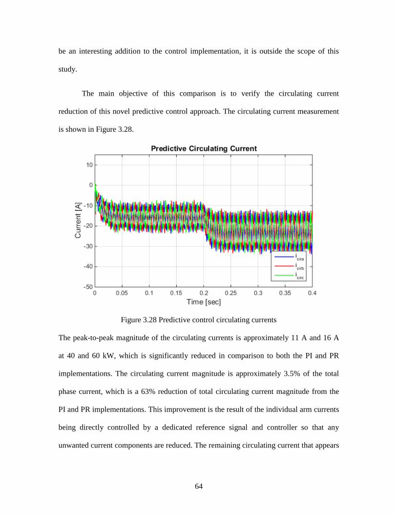
64
be an interesting addition to the control implementation, it is outside the scope of this
study.
The main objective of this comparison is to verify the circulating current
reduction of this novel predictive control approach. The circulating current measurement
is shown in Figure 3.28.
Figure 3.28 Predictive control circulating currents
The peak-to-peak magnitude of the circulating currents is approximately 11 A and 16 A
at 40 and 60 kW, which is significantly reduced in comparison to both the PI and PR
implementations. The circulating current magnitude is approximately 3.5% of the total
phase current, which is a 63% reduction of total circulating current magnitude from the
PI and PR implementations. This improvement is the result of the individual arm currents
being directly controlled by a dedicated reference signal and controller so that any
unwanted current components are reduced. The remaining circulating current that appears

65
is attributed to both the incomplete DC-bus to ground prediction made in the control
design and the efficacy of the capacitor voltage balancing technique.
The high frequency content present in the power output in Figure 3.19 previously
can be attributed to the circulating current harmonic content. Four periods of the
circulating currents are shown in Figure 3.29.
Figure 3.29 Predictive control circulating currents (zoomed)
Lastly, the MMC output voltage for phase 𝑎 is shown in Figure 3.30 below. The
converter’s output matches the grid voltage very well, and there is no visible phase shift.

66
Figure 3.30 MMC AC-side voltages under predictive control
3.4 TOTAL HARMONIC DISTORTION
Because modular multilevel converters are normally connected to a utility grid,
the converter output voltage harmonics could cause grid voltage distortion. One of the
main benefits of the MMC topology is the inherent reduction of harmonics due to the
small incremental changes in output voltage in comparison to conventional VSCs. The
total harmonic distortion (THD) measurement is a way of quantifying the voltage
distortion of a waveform by calculating the ratio of the sum of all harmonic component
power to the power of the fundamental frequency. This measurement was taken for 20
cycles at steady state of the output waveform under each method of current control. The
results are shown in Table 3.2.

67
Table 3.2 THD Measurements
Control Method THD (%)
Proportional Integral (PI) 5.58
Proportional Resonant (PR) 5.51
Predictive (Deadbeat) 4.88
Since the converter has the same modulation and capacitor voltage balancing techniques,
the THD is shown to be very similar for all three current control techniques, as expected.

68
CHAPTER 4
CONCLUSION
The intent of this research was to investigate different current control strategies
for a modular multilevel converter and compare the performances of each. Specifically, a
novel approach to predictive control of an MMC with inherent circulating current
reduction was presented and compared to the more conventional strategies of
synchronous proportional-integral and resonant control. To accomplish this goal, a MMC
model was developed using MATLAB and Simulink and a cascaded control scheme was
created to control its operation. From these results, the predictive control approach
presented in this paper is validated as a viable method for current control of an MMC,
and its inherent benefit of reduced circulating current is established.
The design method for each control approach was presented and then individually
validated with simulation results. Then, each control approach was included in the
cascade control loop and the converter’s efficiency, phase current error, and circulating
current magnitude were analyzed and compared. The PI and PR controllers had similar
results, while the predictive controller had about three times as much phase current error
in comparison. The predictive controller also had a 63% reduction in circulating current
compared to the PI and PR models. The circulating current ultimately distorts the
sinusoidal arm currents and leads to increased converter losses, so the reduction of these
currents is clearly an advantage for this control type. Finally, the total harmonic distortion

69
of the MMC’s output voltage was quantified under each current control method and the
predictive controller showed a slight decrease in THD in comparison to the PI and PR
implementations.

70
REFERENCES
[1] A. Lesnicar and R. Marquardt, "An Innovative Modular Multilevel Converter
Topology Suitable for a Wide Power Range," IEEE Bologna PowerTech
Conference, pp. 1-6, 2003.
[2] S. Rohner, S. Bernet, M. Hiller, and R. Sommer, “Modelling, simulation and
analysis of a modular multilevel converter for medium voltage applications,” in
Proc. IEEE Int.Conf. Ind. Technol., Vina del Mar, Chile, 2010, pp. 775-782.
[3] A. Lesnicar, “Neuartiger, modularer mehrpunktumrichter M2C für
netzkupplungsanwendungen,” Ph.D. dissertation, Dept. Elect. Eng. Inf. Technol.,
Univ. of Bundeswehr, Munich, Germany, 2008.
[4] Q. Tu, Z. Xu, H. Huang, and J. Zhang, “Parameter design principle of the arm
inductor in modular multilevel converter based HVDC,” in Proc. Int. Conf. Power
Syst. Technol., Hangzhou, China, 2010, pp. 1–6.
[5] Prawin Ange, Michael and Dr. N. Devarajan, “SVPWM Pattern Generation using
Field Programmable Gate Array Implementation,” IPCSIT, vol. 3, pp. 435-439,
2011.
[6] R. Blackmon, “Analysis of Modulation and Voltage Balancing Strategies for
Modular Multilevel Converters,” M.S. Thesis, Dept. Elect. Engr., Univ. S. Carolina,
Columbia, 2013.
[7] S. Buso and P. Mattavelli, Digital Control in Power Electronics. San Rafael, CA:
Morgan & Claypool, 2006.
[8] Q. Tu, Z. Xu and L. Xu, "Reduced Switching-Frequency Modulation and Circulating
Current Suppression for Modular Multilevel Converters," IEEE Transactions on
Power Delivery, vol. 26, pp. 1-9, 2011.
[9] P. Munch, D. Gorges, M. Izak, and S. Liu, “Integrated current control, energy
control and energy balancing of modular multilevel converters,” in Proc. IEEE 36th
Annu. Conf. Ind. Electron. Soc., 2010, pp. 150-155.
[10] Yan Ma and Lingling Fan, “Integrated control and switching strategy for a grid-
connected modular multilevel converter,” in Power & Energy Soc. Gen. Meeting.,
IEEE, pp.1-5, 26-30 July 2015

71
[11] Middlebrook, R.D., "Topics in Multiple-Loop Regulators and Current-Mode
Programming," in Power Electron., IEEE Transactions, vol.PE-2, no.2, pp.109-124,
April 1987.
[12] N. Mendalek and K. Al-Haddad, "Modeling and nonlinear control of shunt active
power filter in the synchronous reference frame," Harmonics and Quality of Power,
Proc. 9th
Int. Conf., vol. 1, pp. 30-35, 2000.
[13] M. Hagiwara and H. Akagi, "Control and Experiment of Pulsewidth-Modulated
Modular Multilevel Converters," IEEE Transactions on Power Electron., vol. 24,
pp. 1737-1746, 2009.
[14] Hu Pengfei; Jiang Daozhuo; Zhou Yuebin; Guo Jie; Lin Zhiyong, "Study of the
Proportional Resonant Control Based Modular Multilevel Converter," in Digital
Manuf. and Automation (ICDMA), 3rd
Int. Con., pp.810-813, July 31-Aug. 2 2012.
[15] N. Zhang, H. Tang, and C. Yao, “A Systematic Method for Designing a PR
Controller and Active Damping of the LCL Filter for Single-Phase Grid-Connected
PV Inverters,” in Energies, vol.7, no.6, pp.3934-3954, June 2014.
[16] Dumitrescu, A.M.; Griva, G.; Bojoi, R.; Bostan, V.; Magureanu, R., “Design of
current controllers for active power filters using naslin polynomial technique,” in
Power Electron. and Applic., European Conference, pp.1-7, 2-5 Sept. 2007.
[17] Jiangchao Qin; Saeedifard, M., “Predictive control of a three-phase DC-AC Modular
Multilevel Converter," in Energy Conversion Congress and Exposition (ECCE),
IEEE, pp.3500-3505, 15-20 Sept. 2012.
[18] S. Bacca, I. Munteanu and A. I. Bratcu, “Naslin Polynomial Method,” in Power
Electronic Converters Modeling and Control, London, England: Springer-Verlag,
2014, ch. 9,sec. 9.3.3.3, pp. 257-261.

72
APPENDIX A – MEASUREMENT SCHEMATIC
vsa
vsb
vsc
L
Vpa Vpb Vpc
Vdc-
+
_
Vna Vnb Vnc
Ipa Ipb Ipc
Ina Inb Ipc
+ + +
+ + +
ij
Idc
va
vb
vc
Vdc+
+
_
Vpdc-g
Vndc-g
+
_
+
_
Figure A.1 DC-bus voltage variation measurement locations