Embed Size (px)
Citation preview

Comparison of the Josephson Voltage Standards of the LNE and the BIPM
(part of the ongoing BIPM key comparison BIPM.EM-K10.b)
S. Solve and R. Chayramy
Bureau International des Poids et Mesures F- 92312 Sèvres Cedex, France
S. Djorjevic and O. Séron
Laboratoire national de métrologie et d’essais
ZA de Trappes-Élancourt 29, avenue Roger Hennequin
78197 TRAPPES Cedex - France

LNE/BIPM Comparison 2/26
Comparison of the Josephson Voltage Standards of LNE and the BIPM
(part of the ongoing BIPM key comparison BIPM.EM-K10.b)
S. Solve and R. Chayramy
Bureau International des Poids et Mesures F- 92312 Sèvres Cedex, France
S. Djorjevic and O. Séron
Laboratoire national de métrologie et d’essais
ZA de Trappes-Élancourt 29, avenue Roger Hennequin
78197 TRAPPES Cedex - France
Abstract. A comparison of the 10 V Josephson array voltage standard of the Bureau
International des Poids et Mesures (BIPM) was made with that of the Laboratoire National de
Métrologie et d’Essais (LNE), France, in December 2007. The results are in very good agreement
and the estimated combined relative standard uncertainty is 1.1 parts in 1011.
1. Introduction
In the framework of CIPM-MRA Key Comparisons, the BIPM has piloted a direct Josephson array
voltage standard (JAVS) comparison carried out with the Laboratoire National de Métrologie et
d’Essais (LNE), on-site, in December 2007.
This comparison is the first to follow the new version of the technical protocols for BIPM.EM-K10a & b (OPTION A and B*), which were reviewed by the experts designated during the 23rd CCEM (2007) to be member of the CCEM Support Group for BIPM direct on-site Josephson comparisons. The difference with the previous version of the protocol is the insertion of the following rule: “When a significant improvement is obtained during the comparison both the initial and the final results are added to the KCDB with a note, but only the final result appear on the graph of results.”
This article describes the technical details of the experiments which were carried out to achieve
the final result of the comparison.
* Option A is the scheme where the BIPM measures the JVS of the participant with its measurement setup. Option B is the other way round.

LNE/BIPM Comparison 3/26
2. Comparison equipment
2.1 The BIPM JAVS
The part of the BIPM JAVS used in this comparison comprises the cryoprobe with a PTB 10 V SIS
array (S/N: JK-50/11), the microwave equipment and the bias source for the array. The Gunn
diode frequency was stabilized using an EIP 578 counter, and an ETL/Advantest stabiliser. To
visualize the array I-V characteristics, while keeping the array floating from ground, an optical
isolation amplifier was placed between the array and the oscilloscope; during the measurements,
the array was disconnected from this instrument. Usually, an HP 34401A digital voltmeter (DVM) is
inserted between the array voltage bias leads to measure the voltage in order to verify the step
stability. For this exercise, we were unable to do it as the DVM introduced too much noise into the
measurement loop. We tried to change it to an HP34420A equipped with an external filter but we
came to the same conclusion. As it will be reported in the following, we could nevertheless perform
the measurement without monitoring the voltage across the BIPM JVS.
The series resistance of the measurement leads was less than 4 Ω, and the value of the thermal
electromotive forces (EMFs) was found to be 350 – 450 nV. The leakage resistance between the
measurement leads was greater than 5 × 10¹¹ Ω.
2.2 The LNE JAVS
The LNE JAVS is routinely used to calibrate Zener diode based voltage standards.
It operates a 10 V SIS array fabricated at the PTB. The cryoprobe is housed in a thin-walled
stainless steel tube. The microwave part outside the dewar is composed at room temperature of a
metal WR12 waveguide section equipped with a mylar DC break, while the part going in the
Helium dewar, is composed of a dielectric waveguide (10 dB insertion loss) to reduce the helium
consumption. Special care has been taken for the metrological voltage output on top of the
cryoprobe. It consists of two copper blocks which ensure good equilibrium to room temperature.
The laboratory temperature is regulated to better than ± 0.3 K over a week of measurements. This
minimizes the thermal voltages and ensures a good stability of these voltages during the
measurements. A typical value for the thermal electromotive forces (EMFs) is typically about

LNE/BIPM Comparison 4/26
250 nV with a stability of a few nanovolts during the same measurement day (cf figure 1). The
setup is situated in a laboratory, completely covered by thick copper foils, acting as a Faraday
cage that prevents the experiment from external electromagnetic interferences.
The potential leads are filtered from the external noise with a 3-stage 5 kHz LC filter placed in the
cryoprobe head, and present a series resistance of less than 2 Ω. Moreover the Josephson array
chip is surrounded by a cryoperm shield. Four additional copper wires with RF feed-through filters
are used to bias the array with a home-made bias source and to visualize the I-V characteristics of
the array on an analog oscilloscope. These leads are disconnected during the measurements with
the help of a manual switch and then the array is floating from ground.
The microwave frequency of the Gunn diode (73-75 GHz) is driven by an ETL power supply and is
phase locked using an EIP 578B Source Locking Microwave Counter, referenced to a GPS
controlled 10 MHz rubidium clock.
Some further details of the LNE setup are:
• Type of array: 10 V SIS, manufactured by PTB (s/n Me168-3);
• Detector: HP 34420A, used on the 10 mV range without any filter;
• Bias source: Homebuilt LNE Source;
• Oscilloscope: A Tektronix 7603 oscilloscope is used to visualise the steps and to adjust the
RF power level at the beginning of a series;
• Software: Homebuilt software under Labview© environment;
• Frequency source stabilizer: Counter EIP 578B with locking of the frequency to the external
10 MHz reference and a stability better than ±1.5 Hz during the period of the comparison.
The LNE array is irradiated at a frequency around 74.9 GHz;
• Thermal EMF (including array connections): approximately 250 - 350 nV, varies with liquid
He level in the reservoir;
• Total impedance of the two measurement leads:< 2 Ω;
• Leakage resistance of measurement leads: 1.7 × 10¹¹ Ω.

LNE/BIPM Comparison 5/26
0 40 80 120 160 200 240 280 320440
445
450
455
460
Ther
mal
em
f (nV
)
DVM readings
Vdvm+ (nV) Vdvm- (nV)
Fig. 1. Example of the evolution of the thermal emf for the complete measurement loop during the comparison. The full and empty dots represents the measurements in the negative and positive polarities
respectively.
3. Comparison procedures - Option B (LNE’s setup is operated to measure the BIPM JVS)
3.1 First measurements
Once the BIPM equipment has been set up and sufficiently stable conditions have been found the
standard was connected to the LNE’s measurement system and ten measurement points were
acquired following the procedure applied by LNE for routine measurements of Zener standards.
The result was (ULNE − UBIPM) / UBIPM = - 4.3 × 10⁻¹⁰.
The experimental standard deviation of the mean was 1.5 nV.
This comparison result shows the perfect reliability of the LNE DC voltage calibration setup and
confirms the CMCs of the laboratory.

LNE/BIPM Comparison 6/26
Within the week allotted to the comparison, different experiments were carried out in order to
achieve the lowest voltage difference between the two JVS. The stability of both standards, even if
they were connected together, was so satisfactory that many measurement configurations were
tested. All the details of these test measurements are described in Appendix B.
During the measurements, the LNE array was disconnected from its bias source which was
operated on the mains. The BIPM array was operated on batteries during the step adjustment
sequence, and was then disconnected from its bias source. Both JVS were thus floating from
ground during the data acquisition process. The reference ground was chosen to be on the LNE
side. The two arrays were connected in series-opposition via the LNE low thermal-EMF switch,
which was always used in the same position (i.e., “forward” or “positive” position). In this
comparison scheme (option “B”), the LNE JAVS was used to measure the BIPM array voltage as if
it were a Zener voltage standard. During the comparison, only the biases of the two arrays were
reversed and no switch reversal was made. During the polarity reversal, the switch was set to a
position where the nanovoltmeter was measuring the total voltage across the LNE array and its
range was set to automatic.
3.2 Description of the measurements (See also Appendix B)
Operating setup for the first measurements
The following is a brief description of the procedure used by the LNE to obtain a single
measurement of the voltage of the BIPM array. During the comparison, the LNE and BIPM current
bias sources were used to select manually the same step after each polarity reversal. An HP
3458A was used to manually monitor the LNE array voltage during the adjustment phase. A
Labview© program was operated to control the detector and to record the data. The detector was a
digital nanovoltmeter (HP34420A on the 10 mV range). Two sets of 40 readings 10 powerline
cycles each (NPLC=10) are taken, one set in the positive bias polarity of the two arrays, and the
one in the negative polarity. Two successive measurements follow the scheme: +, -, -, +. For each
set, the program acquires 40 readings of the voltage difference measured by the detector. Those
data are transferred to the computer through an optical fiber. The complete series of
measurements (+,-) takes about half a minute when there is no array instability. The readings are
stored in an ASCII datafile and the value attributed to the BIPM standard is also calculated by the
software. The nanovoltmeter gain correction factor and linearity correction are included into the
calculations.

LNE/BIPM Comparison 7/26
Operating setup for the best measurements
The initial LNE measurement setup was modified. The digital nanovoltmeter was replaced by an
EM N11 used on the 1 µV range and the low thermal emf’s switch was replaced by another one
which is equipped with a position for which the EM N11 connectors are short circuited during
polarity reversals. All the details are given in the first paragraph of the appendix B (12 December).
The software procedure to acquire the data was the same as the one used during the first series.
The differences between the values measured by the LNE and the theoretical value of the BIPM
array voltage during the comparison are plotted on Fig. 2.
0 5 10 15 20 25-1,0
0,0
1,0
Measurements
ULN
E-U
BIP
M (n
V)
Fig. 2: Differences between the measured values and the theoretical value of the BIPM array voltage. The dotted line represents the mean value, the dashed lines
(– – –) represent the experimental standard deviation of the mean, and the dotted-dashed lines (––– – ––– ) are the experimental standard deviation. The error bars reflect the Type A uncertainty of a single measurement.
Three series of measurement were made and are presented with different symbols (square, circle and triangle).

LNE/BIPM Comparison 8/26
3.3 Uncertainties and results
The sources of Type B uncertainty (Table 1) are : the frequency accuracy of the Gunn diodes
stabilised with the frequency counter, the leakage currents, and the detector gain and linearity.
Most of the effects of the detector gain and of the frequency stability are already contained in the
Type A uncertainty. As both array polarities were reversed during the measurements, the effect of
the residual thermal EMFs (i.e., non-linear drift) is also already contained in the Type A uncertainty
of the measurements.
Uncertainty/nV
Type BIPM LNE
Frequency 1 B 0.02 0.02
Leakage resistance of the meas. leads 2
B 0.025 0.068
Detector 3 B - 0.002
Total (RSS) B 0.03 0.07
Table 1. Estimated Type B standard uncertainty components.
(1) As both systems were referred to the same 10 MHz frequency reference, only a Type B
uncertainty on the frequency measured by the EIP is included. [1]
(2) A detailed description is given in appendix B.
(3) The detector noise is already contained in the Type A uncertainty of the measurements. The
Type B uncertainty component for the null detector is calculated from the uncertainty on the gain
correction as described in detail in [1]. Appendix B describes the way the gain correction was
measured. This contribution is small as both arrays were biased to the same voltage.

LNE/BIPM Comparison 9/26
The standard deviation of the mean of the 23 measurements was taken as Type A uncertainty and
is equal to 0.08 nV.
The result, expressed as the relative difference between the values that would be attributed to the
10 V Josephson array standard by the LNE (ULNE) and its theoretical value (UBIPM) is:
(ULNE − UBIPM) / UBIPM = -0.7 × 10⁻¹¹ and uc / UBIPM = 1.1 × 10⁻¹¹
where uc is the combined standard uncertainty.
4. Comparison procedures – Option A
As mentioned in the beginning of the third paragraph, experimental conditions met were so
satisfactory that both arrays were able to stay on the same step for several minutes. We thus
decided to switch to an option A comparison for which the LNE JVS was compared to the BIPM
JVS via the BIPM measurement setup.
4.1 Description of the measurements (also See Appendix A)
In the option A scheme, the BIPM uses its equipment to measure the voltage provided by the
participant’s JVS. The BIPM equipment consists of an EM model N1a analog nanovoltmeter
(operated on its 3 µV range) whose output is connected, via an optically-coupled isolation
amplifier, to a pen recorder and a digital voltmeter (DVM) HP34401A which is connected to a
computer.
This computer is used to monitor measurements, acquire data and calculate results. Low thermal
electromotive force switches are used for critical switching, such as polarity reversal of the detector
input. The connection of both arrays in series opposition is also controlled by a low thermal switch.
The equipment includes a voltage divider to prevent the detector from overload if both systems are
no more on the selected steps.
Once the participant’s standard is connected to the BIPM measurement system, measurement
points are acquired according to the following procedure:
1- Positive array polarity and reverse position of the detector;
2- Data acquisition;
3- Positive array polarity and normal position of the detector;
LNE/BIPM Comparison 10/26
4- Data acquisition;
5- Negative array polarity and reverse position of the detector;
6- Data acquisition;
7- Negative array polarity and normal position of the detector;
8- Data acquisition;
9- Negative array polarity and reverse position of the detector;
10- Data acquisition
11- Negative array polarity and normal position of the detector;
12- Data acquisition;
13- Positive array polarity and reverse position of the detector;
14- Data acquisition;
15- Positive array polarity and normal position of the detector;
16- Data acquisition;
The reversal of the detector polarity is done to cancel out any detector offset error and thermo-
electromotive forces.
Each “data acquisition” step consists of 10 preliminary points followed by 30 measurement points.
Each of these should not differ from the mean of the preliminary points by more than twice their
standard deviation, otherwise the data are rejected and the acquisition is restarted. The “data
acquisition” sequence lasts 25 s and is basically the time period during which both arrays are to
stay on the selected step. The total measurement time (including polarity reversals and data
acquisition) is approximately 5 minutes.
This procedure is repeated three times to calculate one measurement point. We measured a total
of sixteen points between the 10th of December and the 11th of December.
The differences between the values measured by the BIPM and the theoretical value of the LNE
array voltage during the option A comparison are plotted in Fig. 3.

LNE/BIPM Comparison 11/26
-0,8
-0,6
-0,4
-0,2
0
0,2
0,4
0,6
0,8
1
1,2
Measurement Number
U L
NE
- U B
IPM
/nV
(opt
ion
A)
10 December 11 December
Fig. 3. Voltage differences between the measured values and the theoretical value of the BIPM array voltage (option A). The dotted (. . . ) represents the mean value, the dashed line (– – –) represent the experimental
standard deviation of the mean, and the dotted-dashed line (––– – ––– ) are the experimental standard deviation.
4.2 Uncertainties and results
The BIPM uncertainty components, type and respective contribution are listed in Table 2:
Uncertainty component Type Contribution / nV
Frequency 1 B 0.02
Leakage resistance of the
meas. leads 2
B 0.025
Detector Calibration 3 A 0.25
Total RSS 0.25
Table 2.: Uncertainty components (k=1) for the voltage difference measurement with the BIPM
equipment 10 V.

LNE/BIPM Comparison 12/26
(1) As both systems are referred to the same 10 MHz frequency reference and most of the effects
of the frequency stability are already contained in the Type A uncertainty, only a Type B
uncertainty for systematic errors of the EIP frequency measurement is included. [1]
(2) A detailed description is given in appendix B.
(3) The BIPM “detector” is corrected for its gain and non-linearity and the comparison is carried out
for a voltage difference between the two quantum standards close to zero. This calibration wasn’t
done for the comparison so we have applied a multiplication factor of two to the typical uncertainty
value (uD=0.12 nV).
The LNE uncertainty components, type and their respective contribution are listed in Table 3:
Uncertainty component Type Contribution / nV
Frequency 1 B 0.02
Leakage resistance of the
meas. leads 2
B 0.068
Total RSS 0.07
Table 3:Uncertainty components (k=1) for the voltage difference measurement with the LNE
measurement setup.
(1) As both systems are referred to the same 10 MHz frequency reference and most of the
effects of the frequency stability are already contained in the Type A uncertainty, only a Type B
uncertainty for systematic errors of the EIP frequency measurement is included [1].
(2) The leakage resistance of the measurement leads was determined during the comparison:
RL (LNE) = 1.7 × 10¹¹ Ω. A detailed description is given in appendix B.
The standard deviation of the mean of the 16 measurement points is considered as the type A
uncertainty and is equal to 0.12 nV.

LNE/BIPM Comparison 13/26
The computation of the data obtained during these two days gives a relative voltage difference of :
(ULNE − UBIPM) / UBIPM = 4.8 × 10⁻¹¹ with a relative combined standard uncertainty of:
uc / UBIPM = 2.9 × 10⁻¹¹
5. Discussion and conclusion
This comparison is the tenth of a new series (started in September 2004) where the host
laboratory uses its own Josephson equipment to measure the voltage of the BIPM array,
considered as the transfer instrument. The main feature of this new measurement technique is that
it requires only the BIPM array, not both arrays, to maintain a perfectly stable and reproducible
10 V output during the measurements.
The BIPM equipment was installed on the very day of arrival. The preliminary measurements
demonstrated the ability of LNE in very high quality 10 V measurements. During the next five days
many modifications were intentionally made (cf. Appendixes) to various parts of the whole system
(assemblage of the BIPM standard and the LNE measurement set-up) in order to identify sources
of noise, to find out some critical parameters and to correct for their influence on the
measurements. We finally came to what we consider the limits of what could be expected in the
comparison of two quantum standards using an analog null detector at room temperature. This
comparison allowed both BIPM and the laboratory to characterise more accurately and improve
the robustness of their equipment and measurement setups.
During the period dedicated to the comparison, we were able to compare the two options of the
BIPM.EM-K10b comparisons. The results are shown on the Fig 4:

LNE/BIPM Comparison 14/26
final results of the two options of the comparison
-0,6-0,4-0,2
00,20,40,60,8
11,21,4
option A (blue) and option B (red)
ULN
E - U
BIP
M /
nV
Fig 4: Both options Final Comparison (uncertainty bars are k=2, 95%). References
6. Final Result
Table 4 presents the results obtained during the comparison in a chronological order:
Date Comparison
Option Type
[(ULNE − UBIPM) / UBIPM]]
± uc / UBIPM
06/12/2007 B (-4.3 ± 1.5) × 10–10
10 to 11/12/2007 A (4.8 ± 2.9) × 10–11
13 to 14/12/2007 B (-0.7 ± 1.1) × 10–11
As the comparison was registered as a BIPM.EM-K10.b – option B comparison and as mentioned in the introduction, the final result is expressed by the two following results:
Initial result: [(ULNE − UBIPM) / UBIPM]] ± uc / UBIPM = (-4.3 ± 1.5) × 10–10
Final result: [(ULNE − UBIPM) / UBIPM]] ± uc / UBIPM = (-0.7 ± 1.1) × 10–11
These two results will be recorded in the KCDB but only the last one will appear on the graph.

LNE/BIPM Comparison 15/26
7. References • [1] Djordjevic S., Solve S., et al., Direct comparison between a programmable and a conventional Josephson voltage standard at the level of 10 V, Metrologia, 2008, 45(4), 429-435
DISCLAIMER
Certain commercial equipment, instruments or materials are identified in this paper in order to adequacy specify the environmental and experimental procedures. Such identification does not imply recommendation or endorsement by the BIPM, nor does it imply that the materials or equipment identified are necessarily the best available for the purpose.

LNE/BIPM Comparison 16/26
Appendix A:
Appendix A describes some details on the option A comparison.
10 December
The equipment configuration was changed in order for the BIPM measurement chain to measure
the LNE JVS. The ground line continuity between the two JVS was ensured through the metallic
outer part of BIPM low thermal emfs switch. The only potential reference was chosen to be on the
LNE He dewar. This configuration is illustrated on the Figure A1.
Fig A1: Details of the connection between the two JVS systems and grounding connections for the option A. Both JVS and the detector were floating from ground during the acquisition sequence. The dashed line shows
the grounding connection of the chassis of the instrumentation required to operate the two JVS.
LNE/BIPM Comparison 17/26
11 December
A particular effort was done to ameliorate the quality of the grounding connections. We used some
copper tape to increase the quality of the electrical contact between each connection.
Furthermore, we thermally protected the JVS measurement output pins by inserting them into a
thermal isolation box. Within the series of measurement, some outliers (at - 4 nV) were sometimes
identified. To verify if they were due to the grounding connection, we tried different configuration:
1- forcing the low side of the LNE array to the ground;
2- switching the main ground connection from the LNE dewar to the BIPM one;
We didn’t manage to identify the source of noise responsible for the presence of those repeatable
outliers. We finally intentionally created a ground loop by connecting both He dewars to the
ground. The mean voltage difference of -0,5 nV changed for the very repeatable value of -2 nV.
We could have expected a higher effect but we came to the conclusion that several low sources of
noise could be responsible for these observations.
At this stage we decided to move back to an option B comparison. This decision was motivated by
the fact that one of the principal objective of this comparison is, for the participant, to identify some
sources of errors and to improve its DC voltage measurement setup.

LNE/BIPM Comparison 18/26
Appendix B
This appendix describes the option B comparison measurements in a chronological manner.
06 December 2007
After having assembled the BIPM equipment, we had to switch to the BIPM backup array as the
critical current of the principal chip showed an abnormal low value compared to the expected value
(50 µA instead of 90 µA). The same low value was obtained after several temperature cycles.
Both JVS systems were grounded to the earth of the laboratory but to avoid any ground loop, the
shielding of the measurements leads weren’t connected together. An LNE low thermal switch was
used to connect or disconnect the two JVS. The negative poles of the two quantum standards
were connected together and the detector was inserted between the positive poles.
The first series of preliminary measurements gave a voltage difference between the two systems
of -4 nV with a standard deviation of the mean of 1.5 nV as mentioned previously (cf. label A on
Figure B1).
The second series of measurements was carried out after connecting the shield of the
measurement leads of the LNE JVS to the cryoprobe housing and by setting a 10 s delay before
running the acquisition. These modifications lead to an improvement in the measurement noise
and we reduced the standard deviation of the mean to 0.7 nV. (cf. label B on Figure B1)
In order to reduce as well the voltage difference we carried out the following modifications on the
setups, but without success:
1- The digital nanovoltmeter was placed between the two negative polarities pins of the JVS. (It
was initially installed between the two positive polarities); (cf. label C on Figure B1)
2- The positive plug of the nanovoltmeter initially on the LNE side was moved to the BIPM side;
(cf. label D on Figure B1).
We managed to reduce the voltage difference to -4×10⁻¹⁰ V with an experimental standard
deviation of the mean of less than 1.8×10⁻⁹ V (for 5 measurements) with the following modification:
3- Both DVMs, an HP3458A on the LNE JVS and an HP34420A on the BIPM side, placed in
parallel to the arrays to monitor their voltage were removed (cf. label E on Figure B1).
4- In the mean time, we changed the acquisition parameters: we reduced the number of points
from 40 to 20 while increasing the power line cycles (NPLC 10) from 2 to 10 in order to keep

LNE/BIPM Comparison 19/26
the same acquisition time (about 5 s) † and see the influence of the integration time of the null
detector. No clear effect was noticed (cf. label F on Figure B1).
A 1 kΩ resistor was added on the positive polarity measurement wire of the BIPM array (cf. label G
on Figure B1).
The 1 kΩ resistor added for the previous series of measurements was removed and the new
series was carried out while keeping the LNE DC biasing source on (i.e. array grounded on one of
his side). (cf. label H on Figure B1).
We carried out a new series after removing the voltmeter (HP34420A) which monitored the voltage
across the BIPM array (cf. label I on Figure B1).
Fig. B1 : Measurement results of the different experiments performed on the very first day of the comparison. The results of the 9 first series of measurements (label A) correspond to the first comparison result. The error
bars represent the experimental deviation of the mean of the measurements.
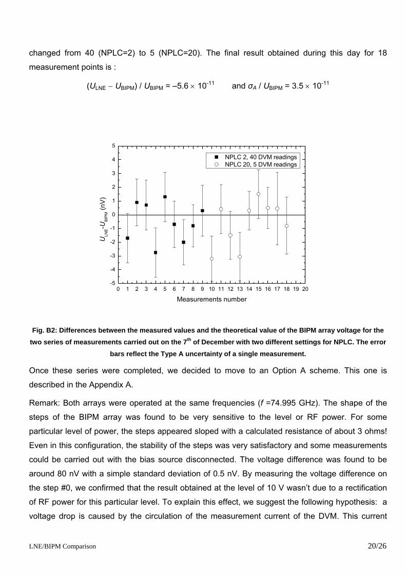
07 December 2007
We repeated two series of measurements (Cf. Fig B2) with the last configuration of the previous
day. We tried two different NPLC settings of the digital null detector (NPLC=2 and NPLC=20) in
order to increase the significant digits of the DVM from 6½ to 7½ digits. For this test the acquisition
time was kept to 5 seconds for both NPLCs which means that the number of readings was
† This short time is required when working with Zener standards but is not the most appropriate for direct Josephson comparisons
LNE/BIPM Comparison 20/26
changed from 40 (NPLC=2) to 5 (NPLC=20). The final result obtained during this day for 18
measurement points is :
(ULNE − UBIPM) / UBIPM = –5.6 × 10⁻¹¹ and σA / UBIPM = 3.5 × 10⁻¹¹
0 1 2 3 4 5 6 7 8 9 10 11 12 13 14 15 16 17 18 19 20-5
-4
-3
-2
-1
0
1
2
3
4
5
NPLC 2, 40 DVM readings NPLC 20, 5 DVM readings
ULN
E-UBI
PM (n
V)
Measurements number
Fig. B2: Differences between the measured values and the theoretical value of the BIPM array voltage for the two series of measurements carried out on the 7th of December with two different settings for NPLC. The error
bars reflect the Type A uncertainty of a single measurement.
Once these series were completed, we decided to move to an Option A scheme. This one is
described in the Appendix A.
Remark: Both arrays were operated at the same frequencies (f =74.995 GHz). The shape of the
steps of the BIPM array was found to be very sensitive to the level or RF power. For some
particular level of power, the steps appeared sloped with a calculated resistance of about 3 ohms!
Even in this configuration, the stability of the steps was very satisfactory and some measurements
could be carried out with the bias source disconnected. The voltage difference was found to be
around 80 nV with a simple standard deviation of 0.5 nV. By measuring the voltage difference on
the step #0, we confirmed that the result obtained at the level of 10 V wasn’t due to a rectification
of RF power for this particular level. To explain this effect, we suggest the following hypothesis: a
voltage drop is caused by the circulation of the measurement current of the DVM. This current

LNE/BIPM Comparison 21/26
should circulate in the array through the measurement leads and the direct effect is to slightly
modify the position of the functioning point on the step.
12 December 2007
After performing an option A comparison, a second option B comparison was carried out using an
analog detector EM N11. The following modifications were made on the LNE setup:
1- After each polarity reversal we waited for 10 seconds before running the acquisition in order
to avoid the larger effects of filter capacitor discharge.
2- A new LNE low thermal emf switch was installed to connect the two JVS. The device is
equipped with a position for which the EM N11 connectors are short circuited. This prevents
the detector to be overloaded when the two JVS are not connected or are not on the same
step.
3- The HP34420A was connected on the isolated output of the EM N11. Its range was forced
to the 1 V range. The voltage offset parameter of the EM N11 was adjusted to compensate
the thermal electromotive forces in order to operate the nanovoltmeter as close as possible
of the zero. Furthermore, a calibration of the zeros (current and voltage) was carried out
following the manufacturer specifications.
4- A calibration of the 1 µV range of the EM N11 (gain error measurement) was carried out by
changing the frequency of the RF power on the BIPM array. Both arrays were biased on the
step N°645 at 74.995 GHz. A change of 100 kHz on the RF signal on the BIPM array leads
to a theoretical change of 133.4 nV on the voltage difference measured by the N11. The null
detector was operated on its lowest filter position (filter 1) during all the comparison period.
The results are shown on the Figure B3:

LNE/BIPM Comparison 22/26
-1000 -800 -600 -400 -200 0 200 400 600 800 1000-3
-2
-1
0
1
2
3
[Um
eas.-U
theo
.] (n
V)
Utheo. (nV)
Fig B3: Deviation from unity gain of the null detector. The deviation of the measured gain from unity is 2.2
× 10-3, and is given by the slope of the linear least square fit of the data.
13 December 2007
During this day, we carried out some measurements for different ranges of the EM N11.
Considering the response time constant of this nanovoltmeter, the NPLC of the HP34420A and the
number of readings were adapted to keep the acquisition time constant with the following
parameters :
1- EM N11:1µV range corresponds to an NPLC=10 on the HP34420A, 40 readings ;
2- EM N11:100 nV range corresponds to an NPLC=10 on the HP34420A, 40 readings ;
3- EM N11:10 nV range corresponds to an NPLC= 50 on the HP34420A, 10 readings ;
The results are presented in the Figure B4. For these parameters, the acquisition was done in the
white noise regime (the white noise level corresponds to about 1.5 nVHz-1/2 [1]). The result
obtained for the three different ranges of the N11 corresponding to 51 measurement points is :
(ULNE − UBIPM) / UBIPM = –8.6 × 10⁻¹² and σA / UBIPM = 5.5 × 10⁻¹²

LNE/BIPM Comparison 23/26
The measurement series of these two last days done on the 1 µV range lead to the final result
mentioned in the report.
0 5 10 15 20 25 30 35 40 45 50 55-2.0
-1.5
-1.0
-0.5
0.0
0.5
1.0
1.5
2.0
Measurements number
(ULN
E-UBI
PM) (
nV)
1µV range 100 nV range 10 nV range
Fig B4: Differences between the measured values and the theoretical value of the BIPM array voltage for three series of measurements of the option B carried out on the 13th of December on the three different ranges of
the N11. The dotted line represents the mean value, the dashed lines (– – –) represent the experimental standard deviation of the mean, and dotted-dashed lines (––– – –––) are the experimental standard deviation.
The error bars reflect the Type A uncertainty of a single measurement.

LNE/BIPM Comparison 24/26
14 December 2007
During this day we ran a series of measurements of the leakage currents to estimate the
uncertainty due to this component.
The leakage resistance, Ri, of the measurement wires in parallel with the measurement leads
resistance, 2rB, is responsible for a voltage drop error on the voltage generated by the JVS. To
calculate the uncertainty component due to these leakage currents, both resistances have to be
measured.
First, to estimate the resistance of the voltage output leads, we carried out a 4-point measurement
of the series resistance of the cryoprobe leads connected to the array at 4 K and we ensured that
the bias current of the ohmmeter (5 µA) was less than the critical current of the array. In addition,
the DC bias current and voltage leads were left open.
Second, the leakage resistance of each JVS was determined from the experiment depicted in
Figure B5.
Fig B5: Schematic of the experiment set up to measure the leakage current between one measurement lead
and the ground.

LNE/BIPM Comparison 25/26
A DVM measures the voltage time dependence across a 1 kΩ resistor (RS) which connects one
side of the array to the ground. The other side, at a potential of 10 V, is left open so that the only
path to ground is through Ri. For both JVS, the bias source is disconnected, therefore Ri stands
only for the isolation resistance of the cryoprobe. These measurements have been carried out in
both polarities successively and Figure B6 presents the comparison of both systems.
At 400 s after the polarity reversal, the leakage current has reached the asymptotic value
corresponding to the value of the apparent insulation resistance. The initial larger voltage is due to
the charging of the capacitors. Within this assumption, the remaining voltage difference between
both polarities (Δe) allows the calculation of the leakage current (iF) according to the formula:
iF = Δe/2Ri.
This method gives much more repeatable results than a direct measurement method with a
Megaohmeter. The results obtained for the two JVS and the corresponding uncertainty component
are listed in Table B1.
0 100 200 300 400 500 600 700 800 900 1000-2.0
-1.5
-1.0
-0.5
0.0
0.5
1.0
1.5
2.0
VBIPM = -8,8 × 10⁻⁸
VBIPM = -1,1 × 10⁻⁷ VLNE = -1.3 × 10⁻⁷ V
VLNE = 2 × 10⁻⁸ V
Time (s)
Vol
tage
(µV
)
LNE +10 V to -10 V BIPM -10 V to +10 V
Fig B6: Discharge through the filter capacitors for both polarity reversal of the two JVS.

LNE/BIPM Comparison 26/26
LNE BIPM
2×rB (Ω) 2 4
iF (pA) 60 11
Ri (Ω) 1.7 × 10¹¹ 9× 10¹¹
Uncertainty (V)
32 U
Rr
i
B ××
6.8 × 10⁻¹¹
2.6 × 10⁻¹¹
Table B1: Uncertainty due to the leakage currents for both Josephson systems.


![40th meeting of the JCRB - BIPM - BIPM · [The corresponding BIPM presentation is available on the restricted-access JCRB working documents webpage as JCRB-40/03.1.] 3.2. BIPM QMS](https://img.pdfslide.net/doc/110x75/6047869895787e1e9f1920f7/40th-meeting-of-the-jcrb-bipm-bipm-the-corresponding-bipm-presentation-is-available.jpg)