Embed Size (px)
Citation preview
C O M P E N S A T I O N OF T H E T H R E S H O L D - V O L T A G E
T E M P E R A T U R E D R I F T IN A D I O D E L I M I T E R
(UDC 621.382.2.088.6)
L. D. K a u r o v
Translated from Izmer i t e l ' naya Tekhnika, No. 9,
pp. 90-91, September, 1966
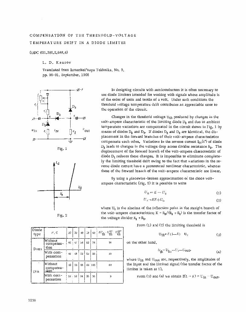
t ~ D2
Dv ~, 0'in e ~ try
type
DI02A
D 18
Fig. 1
Ds
~;I
~ g l U~
d
Fig. 2
In designing circuits with semiconductors i t is often necessary to use diode l imiters intended for working with signals whose ampl i tude is of the order of units and tenths of a volt . Under such conditions the threshold vol tage temperature drift contributes an appreciable error to the operation of the circuit .
Changes in the threshold vol tage Uth produced by changes in the vo l t - ampe re character is t ic of the l imit ing diode D z and due to ambient temperature variations are compensated in the circuit shown in Fig. 1 by
means of diodes D I and D 3. If diodes D 2 and D 3 are ident ical , the dis- p lacement in the forward branches of their vo l t - ampe re characterist ics compensate each other. Variations in the reverse current Irv(t ~ of diode D z leads to changes in the vol tage drop across divider resistance Rz. The displacement of the forward branch of the vo l t - ampe re character is t ic of diode D 1 reduces these changes. It is impossible to e l imina te comple te - ly the l imit ing threshold drift owing to the fact that variations in the re-
verse diode current have a pronounced nonlinear characterist ic , whereas those of the forward branch of the vo l t - ampe re characteris t ic are l inear.
By using a p iecewise-broken approximation of the diode vol t - ampere character is t ic (Fig. 2) i t is possible to write
U B = E - - U 0 (1)
U . = K E + U o , (2)
where U 0 is the abscissa of the inf lect ion point in the straight branch of the vo l t - ampe re characteristics; K = Rz/(R 1 + R 2) is the transfer factor of
the vol tage divider R I + ~ .
t ~ c
Without compensa- tion 17r 40 . 54 62 76 36
With com- 46 48 I 50 53 56 I0 pensation ]
Without 42 53 I 66 84 106 64 compensa- I t_~n
With corn- 33 [ 33 34 35 36 3
I
pensation I
From (1) and (2) the l imit ing threshold is
Uth = E ( l - - K ) - - U0
on t h e other hand,
(3)
Oth Uin--U~176 (4)
where Uin and Uout are, respect ively, the ampli tudes of the input and the l imi ted signal (the transfer factor of the l imi ter is taken as 1).
From (3) and (4) we obtain E(1 - K) = Uin -- Uou t.
1230
It is possible to de te rmine from the above expression for a given E the va lue of the transfer factor K:
Uin - - U out K = I
E (5)
From the va lue of the transfer factor K thus obtained, we find the va lue of Rz:
AUfw(t~ (t') R2, (6)
where AUfw(t ~ is the d isp lacement of the forward branch of the diode D 1 v o l t - a m p e r e character is t ic ; Alrv(t ~ is the
var ia t ion in the reverse current of diode Dz; AUfw(t~ =jAt~ AI (t*) = I tz -- I tl ; j is the forwaxd-voltage t empera - rV r v r v
ture coeff ic ient which for germanium diodes is equal to 2.2-2.5 m V / d e g , and for si l icon diodes to 1.85-1.95 m V / d e g .
At ~ = t 2 - - t l .
The values of I ~ and Irtl v axe taken from reference data or ca lcula ted .
From (6) we obtain
Rz -- A Ufw (t ~ K , R1 __ R~ - - K____~R~ A i r v (t ~ g
The tab le shows the measured pulse ampli tudes at the output of a compensated and a noncompensated l imi ter . In assembling the c i rcui t the diodes are not selected.
1231

![el1 cours4 2017 [Mode de compatibilité] - UQAC · • On voudrait donc limiter le courant pour protéger la diode: +-R +-Le manufacturier indique toujours une valeur limite pour](https://img.pdfslide.net/doc/110x75/5c91a63709d3f258468c1acc/el1-cours4-2017-mode-de-compatibilite-on-voudrait-donc-limiter-le-courant.jpg)