Embed Size (px)
Citation preview

L. Nielen 1,2, A. Siemon 1,2, S. Tappertzhofen 1,2,3, R. Waser 1,2,4,
S. Menzel 2,4, E. Linn 1,2
1 Institut für Werkstoffe der Elektrotechnik II, RWTH Aachen University, Germany
2 JARA – Fundamentals of Future Information Technology
3 Department of Engineering, University of Cambridge, United Kingdom
4 Peter Grünberg Institut 7, Forschungszentrum Jülich GmbH, Jülich, Germany
Complementary Resistive Switch based Neuromorphic Associative Capacitive Network
21.01.2015
Slide 2 Lutz Nielen
Outline
Associative Capacitive Networks
a Neuronal application for non-volatile memories
Complementary Resistive Switches (CRS)
a solution of the sneak path problem in passive ReRAM arrays
Capacitive Readout of CRS cells
CRS-based Associative Capacitive Network (ACN)
Experimental ACN circuitry
Simulative evaluation
Summary

Slide 3 Lutz Nielen
• Information stored via capacitance value
• Simultaneous activation function on all lines
• Summarized output
Content Addressable Memory
Problem with conventional ACNs:
Capacitances charge is volatile
CRS based solution:
non-volatile memory
Applications area:
- Pattern recognition
- Fast routing (reprogrammable lookup-tables)
Associative Capacitive Network - Motivation
O. Kavehei, E. Linn et al., Nanoscale, 5, 5119 (2013)
Artificial neuron model

Slide 4 Lutz Nielen
Content Addressable Memories (CAM)
Classical SRAM based
CAM cell
10-T NOR-type CAM
9-T NAND-type CAM
Rewritable memory with lookup-table functionality
Pattern matching in a single cycle
K. Pagiamtzis; A. Sheikholeslami, IEEE J. Solid-State Circuits, 41, p. 712 (2006)
stored pattern 0 stored pattern 1
stored pattern n-2 stored pattern n-1
stored pattern i
search data register bit lines
n bits
search pattern
en
co
der log2 n
bits
match location
Conventional CAMs are implemented by SRAM core
cells
drawbacks:
static currents high energy consumption
large area demand

Slide 5 Lutz Nielen
Complementary Resistive Switches (CRS)
Overcoming the Sneak Path Obstacle in
passive resistive arrays
Element A
Element B
E. Linn, R. Rosezin et al., Nat. Mater., 9, p. 403 (2010)
Two anti-serially connected elements
• Overall high cell resistance
• No pattern dependency
• Low static power losses
No sneak paths
CRS
CRS state
Element
A
Element
B
resistance
CRS
0 LRS HRS ≈ HRS
1 HRS LRS ≈ HRS
ON LRS LRS LRS+LRS
OFF HRS HRS >> HRS

Slide 6 Lutz Nielen
Capacitive Read-out
S. Tappertzhofen, E. Linn et al., Nanotechnology, 22, p. 395203 (2011)
Capacitive voltage divider
CRS cells offer a capacitive voltage
divider property
• Both elements A and B are equal
in terms of resistive switching
• But: capacitances differ (e.g.
different areas)
• Capacitive read-out of the stored
state
NDRO

Slide 7 Lutz Nielen
CRS-based Associative Capacitive Network
Single ACN cell
N×2N-ACN array
O. Kavehei, E. Linn et al., Nanoscale, 5, 5119 (2013)

Slide 8 Lutz Nielen
ACN – 2-bit Example
O. Kavehei, E. Linn et al., Nanoscale, 5, 5119 (2013)
Stored pattern: 0 1 and negated pattern 1 0
HD=2: maximum output (x1= ‘1’ x2= ‘0’ ) [mismatch]
HD=1: equal output for x1= ‘0’ x2= ‘0’ and x1= ‘1’ x2= ‘1’ [50 % match]
HD=0: minimum output (x1= ‘0’ x2= ‘1’ ) [match]
Output voltage reflects Hamming Distance (HD)
Pattern matching
0.6
1.8

Slide 9 Lutz Nielen
Fabrication of ACN Cells
• Die mounting in a 28 pin
carrier
• Contacting via wedge-wedge
bonding with gold wires
• Evaluation with an
experimental circuitry
Cell A: 24×10 µm²
Cell B: 20×20 µm²
Fabrication of a
µ-structure array
• Silicon wafer
• Platinum, Titanium and
TiO2 sputter deposition
• UV-lithography
Associative Capacitive Network • N×2M array of CRS devices
• green: stored template (T)
• yellow: stored negates of T (T)
• input: vector X and X

Slide 10 Lutz Nielen
Experimental Setup for ACN Read-Out
all bit lines
Generation of the
search pattern by
mechanical switches
L. Nielen; S. Tappertzhofen et al., IEEE SNW, p. 61 (2014)
Appling the search pattern

Slide 11 Lutz Nielen
Experimental Setup for ACN Read-Out
Impedance conversion on
each word line

Slide 12 Lutz Nielen
Experimental Setup for ACN Read-Out
Voltage-to-time conversion
HD detection via switching event

Slide 13 Lutz Nielen
Experimental Results
Stored patterns:
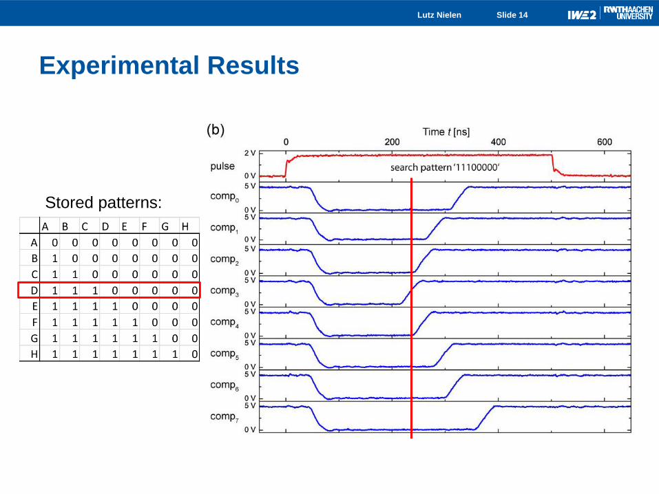
Slide 14 Lutz Nielen
Experimental Results
Stored patterns:
Slide 15 Lutz Nielen
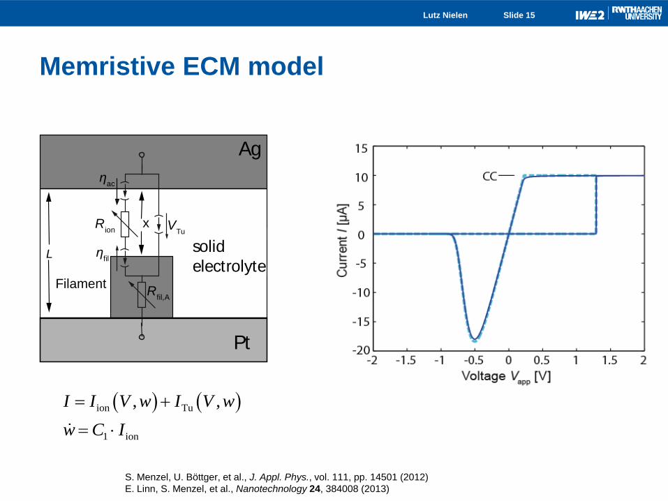
Memristive ECM model
ηac
ηfil
VTu
L
x
solid
electrolyte
Rion
Rfil,A
Filament
Pt
Ag
ion Tu
1 ion
, ,
I I V w I V w
w C I
S. Menzel, U. Böttger, et al., J. Appl. Phys., vol. 111, pp. 14501 (2012)
E. Linn, S. Menzel, et al., Nanotechnology 24, 384008 (2013)

Slide 16 Lutz Nielen
L. Nielen, A. Siemon et al., accepted Jetcas, (2015)
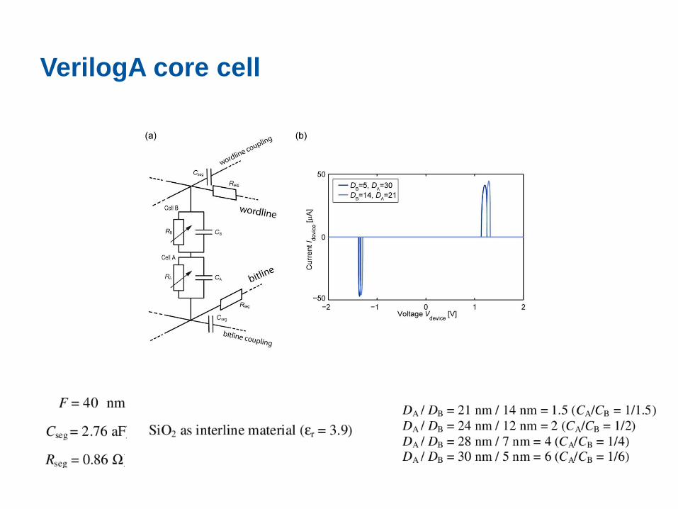
VerilogA core cell

Slide 17 Lutz Nielen
ACN Array Simulations Memristive ECM model
implementation with
VerilogA (SPICE)
Array simulations
performed by Cadence
Spectre
Features
Complete write and
search operation
feasible
Implementation of
coupling capacitances
Different device
capacitance ratios
L. Nielen, A. Siemon et al., accepted Jetcas, (2015)
Slide 18 Lutz Nielen
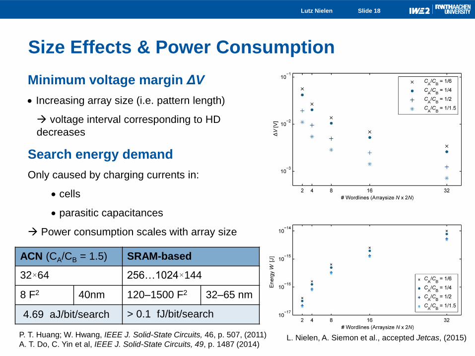
Size Effects & Power Consumption
Minimum voltage margin ΔV
Increasing array size (i.e. pattern length)
voltage interval corresponding to HD
decreases
Search energy demand
Only caused by charging currents in:
cells
parasitic capacitances
Power consumption scales with array size
ACN (CA/CB = 1.5) SRAM-based
32×64 256…1024×144
8 F2 40nm 120–1500 F2 32–65 nm
4.69 aJ/bit/search > 0.1 fJ/bit/search
L. Nielen, A. Siemon et al., accepted Jetcas, (2015) P. T. Huang; W. Hwang, IEEE J. Solid-State Circuits, 46, p. 507, (2011)
A. T. Do, C. Yin et al, IEEE J. Solid-State Circuits, 49, p. 1487 (2014)

Slide 19 Lutz Nielen
• Neuromorphic application for Memristive Random Access Memories was
demonstrated
• An Associative Capacitive Network was fabricated
• Development of an Experimental Setup for ACN Evaluation
• Proof-of-Concept: The ACN shows the predicted behavior
• Study of arrays promises Low Power Consumption
• Fully parallel search within the range of Nanoseconds was demonstrated
using a simple measurement setup
Advantages of CRS based ACN concept:
– Hamming Distance detection (similarity)
– Fully passive 2-CRS cell implementation – small area demand
– Non-volatile No Refresh Low Power Consumption
– No reprogramming fast read access
– No requirement of constant voltage supply
Summary

THANK YOU FOR YOUR ATTENTION

Content Addressable Memories (CAM)
10-T NOR-type CAM 9-T NAND-type CAM
K. Eshraghian; K. R. Cho et al., IEEE Trans. VLSI, 19, p. 1407 (2011)

Content Addressable Memories (CAM)
K. Pagiamtzis; A. Sheikholeslami, IEEE J. Solid-State Circuits, 41, p. 712 (2006)

Content Addressable Memories (CAM)
A. T. Do, C. Yin et al, IEEE J. Solid-State Circuits, 49, p. 1487 (2014)

Content Addressable Memories (CAM)
P. T. Huang, W. Hwang, IEEE J. Solid-State Circuits, 46, p. 507 (2011)

Content Addressable Memories (CAM)
K. Eshraghian; K. R. Cho et al., IEEE Trans. VLSI, 19, p. 1407 (2011)
5T-2R NOR-type CAM 6T-2R NOR-type CAM
7T-2R NAND-type CAM 7T-2R NOR-type CAM
VerilogA core cell

Monte Carlo Simulations
O. Kavehei, E. Linn et al., Nanoscale, 5, 5119 (2013)
Probability–voltage distribution for seven outputs with HD=0 to 6 that correspond to ML1to ML7. The
solid blue line indicates VTH in our test-bench circuit. Outputs with a voltage amplitude above the
threshold voltage are treated as ‘hit’ and below that are treated as ‘miss’
Probability function (p) of seven top match-
lines with minimum HDs versus VML. The
detection probability can be interpreted as p.
In order to detect HD=0, (ML1), with p=95%
chance, VTH has to be around 1.5 V. Under
these circumstances a successful detection
over a range of outputs is achieved. If HD=0,
the output is 1 with 95% probability. For HD=1,
the output is 1 with 50% probability, while for
HD=2 the probability for an output 1 is 10%.
For HD=3, only a probability of 0.5% for
observing an output 1 is given. The probability
that output is 1 for HD > 3 tends to have
negligible small values. Thus, HD < 4 are
detect-able with high probability.


![A Neuromorphic Device Implemented on a Salmon‐DNA … · 2020. 8. 11. · particular, Wang et[41] successfully built a fully memristive al. neural network through the integration](https://img.pdfslide.net/doc/110x75/60b559ddf616081311042b4a/a-neuromorphic-device-implemented-on-a-salmonadna-2020-8-11-particular-wang.jpg)