Embed Size (px)
Citation preview

Complementary wireless module WLAN
Standard Laminate SiP Module
Series/Type: R078 (WL1801) / D7021 Ordering code: B30911D7021Y918
Date: 2014-12-9 Version: 1.3
EPCOS AG 2014. Reproduction, publication and dissemination of this publication, enclosures hereto and the information contained therein without EPCOS' prior express consent is prohibited.
Content of header bars 1 and 2 of data sheet will be automatically entered in headers and footers! Please fill in the table and then change the color to "white". This ensures that the table disappears (invisible) for the customer PDF. Don't change formatting when entering or pasting text in the table and don't add any cell or line in and to it!
Identification/Classification 1 (header 1 + top left bar):
Complementary wireless module WLAN
Identification/Classification 2 (header 2 + bottom left header bar):
Standard Laminate SiP Module
Ordering code: (top right header bar) B30911D7021Y918
Series/Type: (bottom right header bar) R078 (WL1801) / D7021
Preliminary data (optional): (if necessary)
Department: SAW IT
Date: 2014-12-9
Version: 1.3
DISTRIBUTED BY TEXIM EUROPE

Complementary wireless module WLAN B30911D7021Y918
Standard Laminate SiP Module R078 (WL1801) / D7021
SAW IT 2014-12-9
Please read Cautions and warnings and Page 2 of 35 Important notes at the end of this document.
1 Overview This document details the specifications and features of R078 (WL1801) / D7021 SiP module. The R078 (WL1801) / D7021 SiP module is based on Texas Instruments WL1801 IC, specifically WL180x Data Sheet version 1.2, such that the SiP module specification is subject to any subsequent changes in applicable Texas Instruments documentation and software. The R078 (WL1801) / D7021 contains the WL1801 SoC, 2.4GHz SPDT switch, 2.4GHz band pass filter / diplexer and necessary passive components for WLAN in a highly integrated solution.
1.1 Features
WLAN on a single chip provides universal connectivity in small PCB footprint.
Provides efficient direct connection to battery by employing several integrated switched mode power supplies (DC2DC).
Based on 45nm CMOS technology using proven core technology.
Seamless integration with TI OMAP™ Application Processors.
WLAN core software and hardware are compatible with prior WL127x and WL128x offerings, for smooth migration to Device.
SDIO for WLAN.
Downloadable patches and firmware enables new features to be added for all functional block's.
Temperature detection and compensation mechanism ensures minimal variation in the RF performance over the entire temperature range.
1.2 Applications
Mobile phone and mobile computer device applications.
1.3 General Description
The R078 (WL1801) / D7021 is a highly integrated WLAN device that forms a complete standalone communication system. The WL1801 is a highly integrated single-chip CMOS (45-nm process) incorporates the core functionality of the WL1271/3 and WL1281/3 devices.
The device is the 8th-generation WLAN device from Texas Instruments. As such, the WL1801 is based upon proven core technology and complements the TI integrated devices for connectivity portfolio.
R078 (WL1801) / D7021 is ideal for use in mobile phone and mobile computer device applications due to its low current, small area and cellular phone coexistence-friendly features.
DISTRIBUTED BY TEXIM EUROPE

Complementary wireless module WLAN B30911D7021Y918
Standard Laminate SiP Module R078 (WL1801) / D7021
SAW IT 2014-12-9
Please read Cautions and warnings and Page 3 of 35 Important notes at the end of this document.
1.4 Terms and abbreviations
BPF – Band-Pass Filter
FE – Front-End (refers to FE IC and BPF)
GND – Ground
IC – Integrated Circuit
I/O – Input/Output interfaces
LDO – Low Drop-Out (voltage regulator)
PCB – Printed Circuit Board
Q – Quality factor
RF – Radio Frequency
RX – Receive
SiP – System in Package
SoC – System on Chip
TX – Transmit
Vbat – Battery Voltage
VIO – external pre-existing 1.8V IO power supply
WLAN – Wireless Local Area Network
1.5 Reference documents
Texas Instruments WL180x_Data_Manual_Rev_1_2.pdf
DISTRIBUTED BY TEXIM EUROPE

Complementary wireless module WLAN B30911D7021Y918
Standard Laminate SiP Module R078 (WL1801) / D7021
SAW IT 2014-12-9
Please read Cautions and warnings and Page 4 of 35 Important notes at the end of this document.
1 OVERVIEW ................................................................................................................................................................... 2
1.1 FEATURES ................................................................................................................................................................ 2
1.2 APPLICATIONS.......................................................................................................................................................... 2
1.3 GENERAL DESCRIPTION ........................................................................................................................................... 2
1.4 TERMS AND ABBREVIATIONS .................................................................................................................................... 3
1.5 REFERENCE DOCUMENTS ......................................................................................................................................... 3
2 FUNCTIONAL BLOCK FEATURES ......................................................................................................................... 5
2.1 FUNCTIONAL BLOCK DIAGRAM ............................................................................................................................... 5
2.2 WLAN FEATURES ................................................................................................................................................... 6
3 DETAILED DESCRIPTION ........................................................................................................................................ 7
3.1 HOST INTERFACES.................................................................................................................................................... 7
3.2 CLOCKS AND POWER MANAGEMENT ....................................................................................................................... 7
3.3 WLAN FUNCTIONAL BLOCK ................................................................................................................................. 11
3.4 TERMINAL ASSIGNEMENTS .................................................................................................................................... 12
3.5 TERMINAL FUNCTIONS ........................................................................................................................................... 13
4 DESIGN GOAL SPECIFICATIONS ......................................................................................................................... 19
4.1 GENERAL CHIP REQUIREMENTS AND OPERATION .................................................................................................. 19
4.2 WLAN RF PERFORMANCE .................................................................................................................................... 22
4.3 INTERFACE TIMING CHARACTERISTICS .................................................................................................................. 25
4.4 PACKAGE MECHANICAL DRAWING ........................................................................................................................ 27
4.5 SCHEMATIC ............................................................................................................................................................ 28
5 LEAD-FREE PRODUCT STATUS ........................................................................................................................... 29
6 RECOMMENDED REFLOW PROFILE ................................................................................................................. 30
7 PACKING INFORMATION ...................................................................................................................................... 31
8 REVISION HISTORY................................................................................................................................................. 34
DISPLAY OF ORDERING CODES FOR EPCOS PRODUCTS .................................................................................... 34
DISTRIBUTED BY TEXIM EUROPE

Complementary wireless module WLAN B30911D7021Y918
Standard Laminate SiP Module R078 (WL1801) / D7021
SAW IT 2014-12-9
Please read Cautions and warnings and Page 5 of 35 Important notes at the end of this document.
2 Functional Block Features
2.1 Functional Block Diagram
Figure 2-1 shows a high-level view of R078 (WL1801) / D7021 along with its various configurations.
The flexibility of the R078 (WL1801) / D7021 based on WL1801 enables easy integration with various host-system topologies.
Figure 2-1 High-Level System Diagram
DISTRIBUTED BY TEXIM EUROPE
Complementary wireless module WLAN B30911D7021Y918
Standard Laminate SiP Module R078 (WL1801) / D7021
SAW IT 2014-12-9
Please read Cautions and warnings and Page 6 of 35 Important notes at the end of this document.
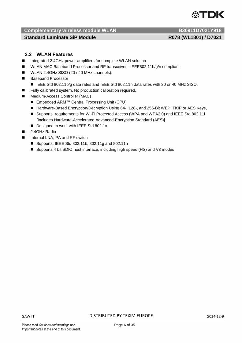
2.2 WLAN Features
Integrated 2.4GHz power amplifiers for complete WLAN solution
WLAN MAC Baseband Processor and RF transceiver - IEEE802.11b/g/n compliant
WLAN 2.4GHz SISO (20 / 40 MHz channels).
Baseband Processor
IEEE Std 802.11b/g data rates and IEEE Std 802.11n data rates with 20 or 40 MHz SISO.
Fully calibrated system. No production calibration required.
Medium-Access Controller (MAC)
Embedded ARM™ Central Processing Unit (CPU)
Hardware-Based Encryption/Decryption Using 64-, 128-, and 256-Bit WEP, TKIP or AES Keys,
Supports requirements for Wi-Fi Protected Access (WPA and WPA2.0) and IEEE Std 802.11i
[Includes Hardware-Accelerated Advanced-Encryption Standard (AES)]
Designed to work with IEEE Std 802.1x
2.4GHz Radio
Internal LNA, PA and RF switch
Supports: IEEE Std 802.11b, 802.11g and 802.11n
Supports 4 bit SDIO host interface, including high speed (HS) and V3 modes
DISTRIBUTED BY TEXIM EUROPE

Complementary wireless module WLAN B30911D7021Y918
Standard Laminate SiP Module R078 (WL1801) / D7021
SAW IT 2014-12-9
Please read Cautions and warnings and Page 7 of 35 Important notes at the end of this document.
3 Detailed Description
3.1 Host Interfaces
3.1.1 WLAN SDIO Transport Layer
The SDIO is the host interface for WLAN. The interface between the host and the D7021 uses an SDIO interface and supports a maximum clock rate of 50MHz.
The Device SDIO also supports the following features of the SDIO V3 specification:
4 bit data bus
Synchronous and Asynchronous In-Band-Interrupt
Default and High-Speed (50MHz) timing
Sleep/wake commands
SDIO timing specifications are given in specification section at end of document.
3.2 Clocks and Power Management
3.2.1 Slow Clock / RTC clock
The slow clock is a free-running clock of 32.768 KHz which is supplied from an external clock source. It is connected to the RTC_CLK pin and is a digital square-wave signal in the range of 0-1.8V nom.
3.2.2 Fast Clock System
3.2.2.1 Fast clock using external crystal
The devices incorporate an internal crystal oscillator circuit for supporting a cost optimized crystal based fast clock scheme. Connection is as shown:
Figure 3-1 XTAL Connection
C1 = C2. Typically 8 - 22pF. Refer to Crystal manufacturer’s recommendations.
R = 390K ohm (+/- 5% tolerance).
DISTRIBUTED BY TEXIM EUROPE
Complementary wireless module WLAN B30911D7021Y918
Standard Laminate SiP Module R078 (WL1801) / D7021
SAW IT 2014-12-9
Please read Cautions and warnings and Page 8 of 35 Important notes at the end of this document.
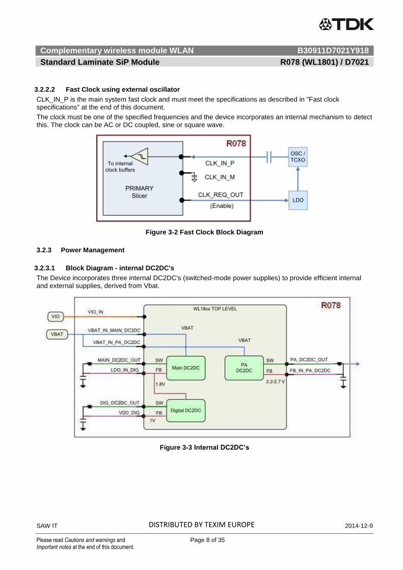
3.2.2.2 Fast Clock using external oscillator
CLK_IN_P is the main system fast clock and must meet the specifications as described in "Fast clock specifications" at the end of this document.
The clock must be one of the specified frequencies and the device incorporates an internal mechanism to detect this. The clock can be AC or DC coupled, sine or square wave.
Figure 3-2 Fast Clock Block Diagram
3.2.3 Power Management
3.2.3.1 Block Diagram - internal DC2DC's
The Device incorporates three internal DC2DC's (switched-mode power supplies) to provide efficient internal and external supplies, derived from Vbat.
Figure 3-3 Internal DC2DC’s
DISTRIBUTED BY TEXIM EUROPE

Complementary wireless module WLAN B30911D7021Y918
Standard Laminate SiP Module R078 (WL1801) / D7021
SAW IT 2014-12-9
Please read Cautions and warnings and Page 9 of 35 Important notes at the end of this document.
3.2.4 Reset / Power up system
After Vbat and VIO are fed to Device and while WLAN_EN are de-asserted (LOW), the device is in Shutdown state.
While in Shutdown state all functional blocks, internal DC2DC's and LDO's will be disabled. The power supplied to the functional blocks is cut off.
When one of the two signals WLAN_EN are asserted (High) a Power On Reset (POR) is performed.
Stable Slow Clock, VIO and Vbat are pre-requisites for successful POR.
3.2.4.1 Chip Top-level Power Up Sequence
Figure 3-4 Chip Top-level Power Up Sequence
DISTRIBUTED BY TEXIM EUROPE
Complementary wireless module WLAN B30911D7021Y918
Standard Laminate SiP Module R078 (WL1801) / D7021
SAW IT 2014-12-9
Please read Cautions and warnings and Page 10 of 35 Important notes at the end of this document.
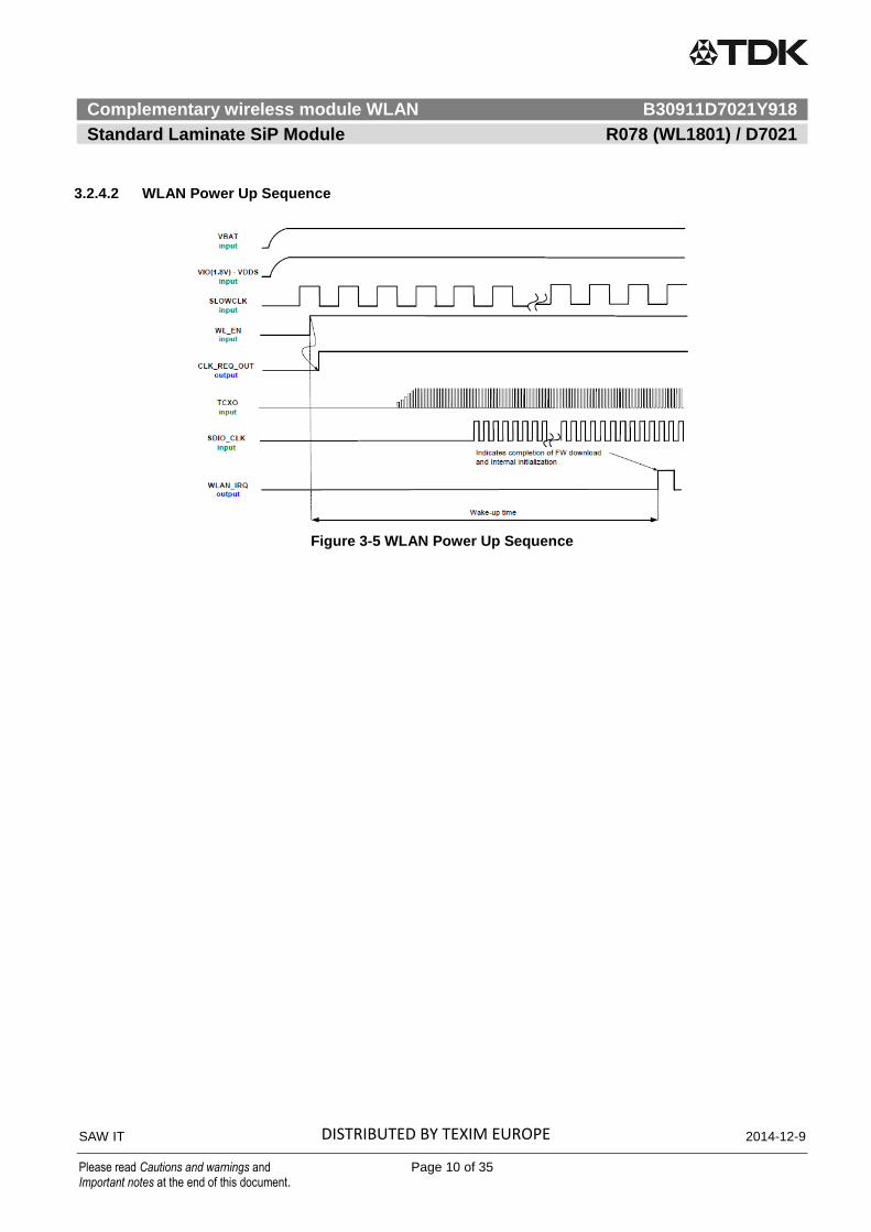
3.2.4.2 WLAN Power Up Sequence
Figure 3-5 WLAN Power Up Sequence
DISTRIBUTED BY TEXIM EUROPE

Complementary wireless module WLAN B30911D7021Y918
Standard Laminate SiP Module R078 (WL1801) / D7021
SAW IT 2014-12-9
Please read Cautions and warnings and Page 11 of 35 Important notes at the end of this document.
3.3 WLAN Functional Block
3.3.1 WLAN MAC
R078 (WL1801) / D7021 MAC implements the IEEE standard 802.11 MAC sub-layer using both dedicated hardware and embedded firmware. The MAC hardware implements real-time functions, including access protocol management, encryption and decryption.
3.3.2 WLAN Baseband Processor
R078 (WL1801) / D7021 baseband processor implements the IEEE 802.11b/g/n PHY sub layers and has been optimized to perform well in conditions of high multipath and noise.
3.3.3 WLAN RF Radio
R078 (WL1801) / D7021 WLAN radio is a highly integrated radio processor designed for 802.11b/g/n applications, including internal front-end PA's.
3.3.4 WLAN RF Configuration and Power Options
The R078 (WL1801) / D7021 includes RF switch, band pass filter and diplexer for complete WLAN (SISO) RF system.
Figure 3-6 R078 (WL1801) / D7021 SISO configuration
3.3.4.1 SISO configuration (WL1801 device)
The diagram above shows WLAN pins in standard SISO application.
DISTRIBUTED BY TEXIM EUROPE

Complementary wireless module WLAN B30911D7021Y918
Standard Laminate SiP Module R078 (WL1801) / D7021
SAW IT 2014-12-9
Please read Cautions and warnings and Page 12 of 35 Important notes at the end of this document.
3.4 Terminal Assignements
The view is from top side: A B C D E F G H J K L M N P
12 GND NU GND VIO GND GND GND GND NU NU NU NU GND GND 12 DIGITAL
11 GND NU GND GND GNDSDIO_D2_
WL
SDIO_CLK
_WLGND NU GND NU GND GND NU 11 RF
10 GND NU GND NU GNDSDIO_D3_
WL
SDIO_D0_
WLGND
DC2DC_R
EQ_MODE
_SOC
CLK_REQ
_OUTGND GND GND GND 10 Power
9 GND GND GND NU GNDSDIO_CM
D_WL
SDIO_D1_
WLGND
SLOW_CL
KNU NU GND GND NU 9 GND
8 NU GND NU NU GND GND GND
COEX_M
WS_BT_W
L_TX_O
COEX_M
WS_FRAM
E_SYNC
NU NU GND GND NU 8 CLOCK
7 GND GND NU GND GND
COEX_M
WS_ACTI
VE
RX_SW_F
EM_WL
COEX_M
WS_RX_P
RI
NU NU GND GND GND NU 7
DIGITAL
High
Speed
6 NU GNDPBIAS_TE
STP_WGND GND
DC2DC_R
EQ_OUT_
SOC
WLAN_IR
QNU GPIO_2 NU NU GND GND NU 6 Not Used
5 GND GNDPDET_TE
STM_WGND GND GND
WLAN_EN
_SOC
FEM_PA_
EN_WLNU GPIO_1 GND GND GND GND 5
4 GND GND NU GND NU NU NU NU NU GPIO_3 GND VBAT1 VBAT2 VBAT3 4
311bg_ANT
_1GND GND GND GND GND GND GND GND GND GND GND GND GND 3
2 GND GND GND GND GND CLK_IN_P CLK_IN_M GND GND GND GND GND GND GND 2
1 GND GND GND GND GND GND GND GNDPA_DC2D
C_IN
PA_DC2D
C_OUTGND GND GND GND 1
A B C D E F G H J K L M N P
Top view
Figure 3-7 Terminal Assignements
DISTRIBUTED BY TEXIM EUROPE

Complementary wireless module WLAN B30911D7021Y918
Standard Laminate SiP Module R078 (WL1801) / D7021
SAW IT 2014-12-9
Please read Cautions and warnings and Page 13 of 35 Important notes at the end of this document.
3.5 Terminal Functions
Pin names and pin numbers in bracket apply to WSP pin out.
Table 3-3 Terminal Functions
Module Pin Name (WSP Pin Name)
Module Pin No. (WSP ball no.)
I/O Type
Shut Down state
Default after POR
Buffer Type [mA]
Description
WLAN pins: I/O signals
SDIO_CLK_WL (SDIO_CLK_WL) G11 (E11) IN HiZ HiZ WLAN SDIO clock. Must be driven by the host.
SDIO_CMD_WL(SDIO_CMD_WL) F9 (D8) IN HiZ HiZ WLAN SDIO command in. Host must pull up.
SDIO_D0_WL (SDIO_D0_WL) G10 (E10) I/O HiZ HiZ WLAN SDIO data bit 0. Host must pull up.
SDIO_D1_WL (SDIO_D1_WL) G9 (E9) I/O HiZ HiZ WLAN SDIO data bit 1. Host must pull up.
SDIO_D2_WL (SDIO_D2_WL) F11 (D11) I/O HiZ HiZ WLAN SDIO data bit 2. Host must pull up.
SDIO_D3_WL (SDIO_D3_WL) F10 (D10) I/O HiZ PU WLAN SDIO data bit 3. Changes state to PU at WL_EN assertion for card detect. Later disabled by the SW during init. Host must pull up.
WLAN_IRQ (IRQ_WL) G6 (E3)
OUT PD Drive 0 SDIO available, interrupt out. Active high. To use WL_RS232_TX/RX lines, need to pull up with 10K resistor.
GPIO_1 (GPIO1) K5 (H1) I/O PD PD Option: WL_RS232_TX (when IRQ_WL = 1 at power up)
GPIO_2 (GPIO2) J6 (H2) I/O PD PD Option: WL_RS232_RX (when IRQ_WL = 1 at power up)
GPIO_3 (UART_DBG_WL) K4 (G4) OUT PU PU WLAN logger Option: GPIO3
FEM_PA_EN_WL (GPIO13)
H5 (F2)
NC
RX_SW_FEM_WL (SW_CTRL_BG_IO1)
G7 (F3) NC
PBIAS_TESTP_W (PABIAS_OUT_FEM_TESTP_WL)
C6 (C7) ANA NC
PDET_TESTM_W (PDET_IN_FEM_TESTM_WL)
C5 (C6) ANA NC
WLAN Pins: RF antenna
11bg_ANT_1 A3 RF WLAN BG RX and TX 50Ω input and output. No external matching required.
Clock pins
CLK_IN_P F2 (E4) ANA FREF/TCXO input for all functional blocks
CLK_IN_M G2 (E5) ANA Connect to GND
SLOW_CLK (RTC_CLK) J9 (H8) ANA Sleep clock 32.768 kHz
CLK_REQ_OUT K10 (K11) OUT PD PD Request external fast clock NC if not used.
DISTRIBUTED BY TEXIM EUROPE

Complementary wireless module WLAN B30911D7021Y918
Standard Laminate SiP Module R078 (WL1801) / D7021
SAW IT 2014-12-9
Please read Cautions and warnings and Page 14 of 35 Important notes at the end of this document.
Module Pin Name (WSP Pin Name)
Module Pin No. (WSP ball no.)
I/O Type
Shut Down state
Default after POR
Buffer Type [mA]
Description
Enable pins
WLAN_EN_SOC (WLAN_EN) G5 (E1) IN PD PD High = enable
Power management pins
VBAT1 M4 POW Battery voltage
VBAT2 N4 POW Battery voltage
VBAT3 P4 POW Battery voltage
VIO D12 POW 1.8V I/O power supply
PA_DC2DC_IN J1 POW PA power supply input, with internal PA_DC2DC connect to pin PA_DC2DC_OUT K1.
PA_DC2DC_OUT K1 POW DC2DC output for PA supply, with internal PA_DC2DC connect to pin PA_DC2DC_IN J1.
DC2DC_REQ_OUT_SOC (NU) F6 (D3) NC
DC2DC_REQ_MODE_SOC (NU) J10 (J10) NC
Co-existence signals
COEX_MWS_RX_PRI (COEX_MWS_UART_RX)
H7 (G5) PU PU General purpose IO. NC if not used.
COEX_MWS_BT_WL_TX_O (COEX_MWS_UART_TX)
H8 (G7) PU PU General purpose IO. NC if not used.
COEX_MWS_ACTIVE (COEX_MWS_PRE_TX)
F7 (G8) PU PU General purpose IO. NC if not used.
COEX_MWS_FRAME_SYNC (COEX_MWS_FRAME_SYNC)
J8 (H7) PU PU General purpose IO. NC if not used.
Not used pins
NU A6 (A4) NC
NU A8 NC
NU B10 (G11) NC
NU B11 (G9) NC
NU B12 (H11) NC
NU C4 (F9) NC
NU C7 (F8) NC
NU C8 (F11) NC
NU D8 (F10) NC
NU D9 (E8) NC
NU D10 (B11) NC
NU E4 (E2) NC
NU F4 (E7) NC
NU G4 (F7) NC
NU H4 (G6) NC
NU H6 (G2) NC
NU J4 (F6) NC
NU J5 (H3) NC
NU J7 (H5) NC
DISTRIBUTED BY TEXIM EUROPE

Complementary wireless module WLAN B30911D7021Y918
Standard Laminate SiP Module R078 (WL1801) / D7021
SAW IT 2014-12-9
Please read Cautions and warnings and Page 15 of 35 Important notes at the end of this document.
Module Pin Name (WSP Pin Name)
Module Pin No. (WSP ball no.)
I/O Type
Shut Down state
Default after POR
Buffer Type [mA]
Description
NU J5 (H3) NC
NU J7 (H5) NC
NU J11 (G10) NC
NU J12 (J8) NC
NU K6 (J4) NC
NU K7 (K4) NC
NU K8 (K5) NC
NU K9 (J7) NC
NU K12 (K8) NC
NU L6 (H6) NC
NU L8 (L7) NC
NU L9 (K7) NC
NU L11 (L11) NC
NU L12 (M10) NC
NU M12 (M9) NC
NC P6 (M7) NC
NC P7 (M5) NC
NU P8 (L5) NC
NU P9 (M6) NC
NU P11 (K6) NC
Ground pins
GND A1 GND
GND A2 GND
GND A4 GND
GND A5 GND
GND A7 GND
GND A9 GND
GND A10 GND
GND A11 GND
GND A12 GND
GND B1 GND
GND B2 GND
GND B3 GND
GND B4 GND
GND B5 GND
GND B6 GND
GND B7 GND
GND B8 GND
GND B9 GND
DISTRIBUTED BY TEXIM EUROPE

Complementary wireless module WLAN B30911D7021Y918
Standard Laminate SiP Module R078 (WL1801) / D7021
SAW IT 2014-12-9
Please read Cautions and warnings and Page 16 of 35 Important notes at the end of this document.
Module Pin Name (WSP Pin Name)
Module Pin No. (WSP ball no.)
I/O Type
Shut Down state
Default after POR
Buffer Type [mA]
Description
GND C1 GND
GND C2 GND
GND C3 GND
GND C9 GND
GND C10 GND
GND C11 GND
GND C12 GND
GND D1 GND
GND D2 GND
GND D3 GND
GND D4 GND
GND D5 GND
GND D6 GND
GND D7 GND
GND D11 GND
GND E1 GND
GND E2 GND
GND E3 GND
GND E5 GND
GND E6 GND
GND E7 GND
GND E8 GND
GND E9 GND
GND E10 GND
GND E11 GND
GND E12 GND
GND F1 GND
GND F3 GND
GND F5 GND
GND F8 GND
GND F12 GND
GND G1 GND
GND G3 GND
GND G8 GND
GND G12 GND
GND H1 GND
GND H2 GND
GND H3 GND
GND H9 GND
DISTRIBUTED BY TEXIM EUROPE

Complementary wireless module WLAN B30911D7021Y918
Standard Laminate SiP Module R078 (WL1801) / D7021
SAW IT 2014-12-9
Please read Cautions and warnings and Page 17 of 35 Important notes at the end of this document.
Module Pin Name (WSP Pin Name)
Module Pin No. (WSP ball no.)
I/O Type
Shut Down state
Default after POR
Buffer Type [mA]
Description
GND H10 GND
GND H11 GND
GND H12 GND
GND J2 GND
GND J3 GND
GND K2 GND
GND K3 GND
GND K11 GND
GND L1 GND
GND L2 GND
GND L3 GND
GND L4 GND
GND L5 GND
GND L7 GND
GND L10 GND
GND M1 GND
GND M2 GND
GND M3 GND
GND M5 GND
GND M6 GND
GND M7 GND
GND M8 GND
GND M9 GND
GND M10 GND
GND M11 GND
GND N1 GND
GND N2 GND
GND N3 GND
GND N5 GND
GND N6 GND
GND N7 GND
GND N8 GND
GND N9 GND
GND N10 GND
GND N11 GND
GND N12 GND
GND P1 GND
GND P2 GND
GND P3 GND
DISTRIBUTED BY TEXIM EUROPE

Complementary wireless module WLAN B30911D7021Y918
Standard Laminate SiP Module R078 (WL1801) / D7021
SAW IT 2014-12-9
Please read Cautions and warnings and Page 18 of 35 Important notes at the end of this document.
Module Pin Name (WSP Pin Name)
Module Pin No. (WSP ball no.)
I/O Type
Shut Down state
Default after POR
Buffer Type [mA]
Description
GND P5 GND
GND P10 GND
GND P12 GND
DISTRIBUTED BY TEXIM EUROPE

Complementary wireless module WLAN B30911D7021Y918
Standard Laminate SiP Module R078 (WL1801) / D7021
SAW IT 2014-12-9
Please read Cautions and warnings and Page 19 of 35 Important notes at the end of this document.
4 Design Goal Specifications
Section Disclaimer
This Specification is based upon the Texas Instruments WL180x Data Sheet version 1.2, and is subject to any subsequent changes in applicable Texas Instruments documentation and software.
Any parameter marked TBD indicates that this is yet to be determined by TDK design/testing. Any parameter marked TBC indicates that this is yet to be determined in an update of Texas Instruments documentation.
4.1 General Chip Requirements and Operation
All parameters are measured as follows unless stated otherwise: VlO=1.8V
4.1.1 Absolute Maximum Ratings (1)
Value Unit
VBAT(2)
-0.5 to 5.5(4)
V
VIO -0.5 to 2.1 V
Input voltage to Analog pins (3)
-0.5 to 2.1 V
Input voltage to all other pins -0.5 to (VDD_IO + 0.5V)
V
Operating ambient temperature range -40 to +85(5)
°C
ESD Stress Voltage (6)
Human Body Model (7)
RF pins >500 V
Other >1000 V
Charged Device Model (8)
RF pins >300 V
Other >250 V
(1) Stresses beyond those listed under “absolute maximum ratings” may cause permanent damage to the device. These are stress ratings only and functional operation of the device at these or any other conditions beyond those indicated under “recommended operating conditions” is not implied. Exposure to absolute-maximum-rated conditions for extended periods may affect device reliability.
(2) The following signals are from the VBAT group: VBAT1, VBAT2, VBAT3
(3) Analog pins: 11bg_ANT_1.
(4) 5.5V up to 10s cumulative in 7 years. 5V cumulative to 250s, 4.8V cumulative to 2.33 years – all includes charging dips and peaks.
(5) Operating free-air temperature range. The device can be reliably operated for 7 years at Tambient of 85˚C, assuming 25% active mode and 75% sleep mode (15,400 cumulative active power-on hours).
(6) Electrostatic discharge (ESD) to measure device sensitivity/immunity to damage caused by electrostatic discharges into the device.
(7) Level listed is the passing level per ANSI/ESDA/JEDEC JS-001. JEDEC document JEP155 states that 500V HBM allows safe manufacturing with a standard ESD control process, and manufacturing with less than 500V HBM is possible if necessary precautions are taken. Pins listed as 1000V may actually have higher performance.
(8) Level listed is the passing level per EIA-JEDEC JESD22-C101E. JEDEC document JEP157 states that 250 V CDM allows safe manufacturing with a standard ESD control process, and manufacturing with less than 250V CDM is possible if necessary precautions are taken. Pins listed as 250 V may actually have higher performance.
DISTRIBUTED BY TEXIM EUROPE

Complementary wireless module WLAN B30911D7021Y918
Standard Laminate SiP Module R078 (WL1801) / D7021
SAW IT 2014-12-9
Please read Cautions and warnings and Page 20 of 35 Important notes at the end of this document.
4.1.2 Recommended Operating Conditions
Rating Condition Sym Min Max Unit
1.8V core supply voltage 1.7 1.95 V
Vbat DC supply range for all modes
3.4 4.3
IO high-level input voltage VIH 0.65 x VDD_IO VDD_IO
IO low-level input voltage VIL 0 0.35 x VDD_IO
Enable inputs high-level input voltage
Vih_en 1.365 VDD_IO
Enable inputs low-level input voltage Vil_en 0 0.4
High-level output voltage @4 mA VOH VDD_lO – 0.45 VDD_IO
@ 1 mA VDD_lO – 0.112 VDD_IO
@0.3 mA VDD_IO- 0.033 VDD_IO
Low-level output voltage @4 mA VOL 0 0.45
@ 1 mA 0 0.112
@0.09 mA 0 0.01
Input transitions time Tr/Tf from 10% to 90% (Digital IO)
(1)
Tr/Tf 1 10 ns
Output rise time from 10% to 90% (Digital pins)
(1)
CL <25 pF Tr 5.3 ns
Output fall time from 10% to 90% (Digital pins)
(1)
CL <25 pF Tf 4.9
Ambient operating temperature -40 +85 °C
(1) Applies to all Digital lines except SDIO, SPI, UART, I2C, PCM and slow clock lines
4.1.3 External Digital Slow Clock Requirements (-40°C to +85°C)
The supported digital slow clock is 32.768 kHz digital (square wave). All core functions share a single input.
Characteristics Condition Sym Min Typ Max Unit
Input slow clock frequency 32768 Hz
Input slow clock accuracy
(initial + temp + aging)
WLAN, BT ±250 ppm
Input transition time Tr/Tf -lO% to 90% Tr/Tf 100 ns
Frequency input duty cycle 15 50 85 %
Input voltage limits Square wave, DC-coupled
Vih 0.65xVDD_IO
VDD_IO Vpeak
Vil 0 0.35xVDD_IO
Input impedance 1 MΩ
Input capacitance 5 pF
DISTRIBUTED BY TEXIM EUROPE
Complementary wireless module WLAN B30911D7021Y918
Standard Laminate SiP Module R078 (WL1801) / D7021
SAW IT 2014-12-9
Please read Cautions and warnings and Page 21 of 35 Important notes at the end of this document.
4.1.4 External fast clock Crystal Requirements and operation (-40°C to +85°C)
Characteristics Condition Min Typ Max Unit
Supported frequencies 26, 38.4 MHz
Frequency accuracy Initial + temp + aging ±20 ppm
Load capacitance, CL(1)
5 13 pF
Equivalent Series Resistance, ESR 60 ohms
Drive level 100 uW
1) Load capacitance, CL = [C1.C2] / [C1 + C2] + CP, where C1, C2 are the capacitors connected on CLK_IN_P & CLK_IN_M respectively and CP is the parasitic capacitance (typically 1-2pF).
For example, for C1 = C2 = 12pF and CP = 2pF, then CL = 8pF.
4.1.5 External TCXO CLK Requirements (-40°C to +85°C)
Parameter Conditions Min Typ Max Unit
Supported frequency 26, 38.4 MHz
Frequency accuracy Total short and long term ±20 ppm
Input voltage limits (TCXO_P) Sine wave/
ac-coupled
2.4GHz WLAN 0.2 1.4 Vp-p
5GHz WLAN 0.8 1.4
Input impedance, 26 MHz
RP Input resistance 20 kΩ
CP Input capacitance 2.5 pF
Input impedance, 38.4 MHz
RP Input resistance 15 kΩ
CP Input capacitance 2.5 pF
Power-up time (1)
5 ms
Phase noise 2.4GHz for 38.4MHz
20MHz SISO (2)
Measured at 1 KHz offset -120 dBc/Hz
Measured at 10 KHz offset -130 dBc/Hz
Measured at 100 KHz offset -135 dBc/Hz
Phase noise 2.4GHz for 38.4MHz
40MHz SISO (2)
Measured at 1 KHz offset -125 dBc/Hz
Measured at 10 KHz offset -132 dBc/Hz
Measured at 100KHZ offset -136.5 dBc/Hz
Phase noise 5GHz for 38.4MHz, 20/40MHz SISO
(2)
Measured at 1 KHz offset -125 dBc/Hz
Measured at 10 KHZ offset -142 dBc/Hz
Measured at 100KHZ offset -145 dBc/Hz
(1) Power-up time is calculated from the time CLK_REQ_OUT asserted till the time the TCXO_CLK amplitude is within voltage limit
specified above and TCXO_CLK frequency is within 0.1 ppm of final steady state frequency.
(2) The phase noise numbers listed here must be met at 38.4 MHz. For other frequencies the phase noise requirement is corrected by adding 20 x log10(fTCXO / 38.4e6) dB. Specifically, for 26 MHz TCXO, the correction factor would be -3.4 dB.
* The slope of the clock at zero-crossings should not be less than that of a 200 mVp-p sine-wave . i.e. 26MHz clock: 16V/μs (for 11bg band) 38.4MHz clock: 24V/μs (for 11bg band)
DISTRIBUTED BY TEXIM EUROPE

Complementary wireless module WLAN B30911D7021Y918
Standard Laminate SiP Module R078 (WL1801) / D7021
SAW IT 2014-12-9
Please read Cautions and warnings and Page 22 of 35 Important notes at the end of this document.
4.2 WLAN RF Performance
All specifications in this draft data sheet are design goal level and subject to change. All specifications have been measured using TDK CB (Carrier Board) and are given at the module pins (Carrier Board insertion loss is de-embedded). All measurements have been performed over VBAT voltage range from 3.4V to 4.3V and over temperature range from -40°C to +85°C.
* 11n 40MHz bandwidth function is available. However the RF performance is guaranteed by only WL180x.
4.2.1 WLAN 2.4 GHz Radio Characteristics
4.2.1.1 WLAN 2.4 GHz Receiver RF Characteristics
Characteristics Condition Min Typ Max Unit
Operation frequency range 2400 2480 MHz
Sensitivity (ANT1) 20MHz bandwidth. At < 10% PER limit
1 Mbps DSSS -91 dBm
54 Mbps OFDM -70
MCS7 -65
Max Input Level At < 10% PER limit
OFDM (11g/n) –19 dBm
CCK –4
Adjacent Channel Rejection at sensitivity level +3 for OFDM and +6 for CCK
2Mbps 42.7 dB 11 Mbps 37.9
54 Mbps 2
LO leakage –80 dBm
4.2.1.2 WLAN 2.4 GHz Receiver Blocking Characteristics Per Band
The R078 (WL1801) / D7021 is designed to coexist with co-located cellular transmitters. Table below lists typical cellular interference sources and the corresponding maximum power from the cellular interference source that can be present at the input terminal of R078 (WL1831) / D7021, such that WLAN receiver sensitivity is not degraded by more than 1 dB. (Further improvement is achieved by antenna isolation)
Characteristics Condition Min Typ Max Unit
Blocking performance at other bands 776 to 794 MHz (CDMA) +10 dBm
824 to 849 MHz (GMSK) +10
824 to 849 MHz (EDGE) +10
824 to 849 MHz (CDMA) +10
880 to 915 MHz (GMSK) +21
880 to 915 MHz (EDGE) +21
1710 to 1785 MHz (GMSK) +3
1710 to 1785 MHz (EDGE) +3
1850 to 1910 MHz (GMSK) -3
1850 to 1910 MHz (EDGE) -3
1850 to 1910 MHz (CDMA) -10
1850 to 1910 MHz (WCDMA) -10
1920 to 1980 MHz (WCDMA) -10
DISTRIBUTED BY TEXIM EUROPE

Complementary wireless module WLAN B30911D7021Y918
Standard Laminate SiP Module R078 (WL1801) / D7021
SAW IT 2014-12-9
Please read Cautions and warnings and Page 23 of 35 Important notes at the end of this document.
4.2.1.3 WLAN 2.4 GHz Transmitter power
RF transmission (Tx) tests are done in continuous transmission.
Characteristics Condition 11bg_ANT_1 pin
Min Typ Max
Maximum output power
1 Mbps +12 +15
11Mbps +12 +15
6 Mbps at EVM: -10 dB, +10 +13
54 Mbps at EVM: -25 dB +9 +12
MCS0 (Greenfield) at EVM: -10 dB
+9 +13
MCS7 (Greenfield) at EVM: -28 dB
+8 +11
Output power accuracy ±1.5
Transmit power control resolution
0.125
4.2.1.4 WLAN 2.4 GHz Transmitter out-of-band emissions
Table below shows 2.4GHz WLAN transmitter out-of-band emissions for each band listed in the Condition column. The wideband noise at 2.4GHz WLAN antenna port is also listed.
Characteristics Condition Min Typ Max Unit
Cellular bands out-of-band broadband emissions(1)
746 to 764 MHz (CDMA1) -145 dBm/Hz
869 to 894 MHz (GSM850) -145
925 to 960 MHz (EGSM900) -138
1570 to 1580 MHz (GPS) -142
1596 to 1609 MHz (GLONASS) -130
1805 to 1880 MHz (DCS1800) -140
1930 to 1990 MHz (PCS1900) -120
2110 to 2170 MHz -129
Cellular bands out-of-band spurious emissions
746 to 764 MHz (CDMA) -44.2(4)
dBm 869 to 894 MHz (CDMA, GSM850) -44.2
(4)
925 to 960 MHz (EGSM900) -44.2(4)
1570 to 1580 MHz (GPS) -44.2(4)
1805 to 1880 MHz (DCS1800) -44.2
(4)
1930 to 1990 MHz (PCS1900, CDMA) -44.2(4)
2110 to 2170 MHz -44.2(4)
Spurious emission during operation at 1MHz RBW
30MHz – 1GHz –55(2)
dBm
2nd
harmonic –33(3)
3rd
harmonic –33(3)
4th harmonic –33
(3)
5th harmonic –33
(3)
(1) Figures are for max transmission power for all available modulations. The setup noise floor is -167dBm/Hz.
(2) Based on TI IC performance
(3) ETSI limit plus 3dB margin
(4) FCC conductive limit plus 3dB margin
DISTRIBUTED BY TEXIM EUROPE

Complementary wireless module WLAN B30911D7021Y918
Standard Laminate SiP Module R078 (WL1801) / D7021
SAW IT 2014-12-9
Please read Cautions and warnings and Page 24 of 35 Important notes at the end of this document.
4.2.1.5 2.4GHz WLAN Current Consumption
Active Current
Spec item (1)
MIN TYP
MAX
Units
Tx 11CCK @15dBm 345 380 mA
Tx 54OFDM @12dBm 290 320 mA
Rx 65 75 mA (1) All measured at ANT1 and the 3.6V VBAT rail of the solution. TCXO current included.
DISTRIBUTED BY TEXIM EUROPE

Complementary wireless module WLAN B30911D7021Y918
Standard Laminate SiP Module R078 (WL1801) / D7021
SAW IT 2014-12-9
Please read Cautions and warnings and Page 25 of 35 Important notes at the end of this document.
4.3 Interface Timing Characteristics
4.3.1 SDIO timing specifications
4.3.1.1 SDIO Switching Characteristics – Default rate input and output
Specification is over recommended operating conditions. Parameters are for default clock frequency.
Figure 4-1 SDIO default input timing
Figure 4-2 SDIO default output timing
Table 4-1 SDIO Switching Characteristics – Deault Rate
Parameter Min Max Unit
fclock Clock frequency, CLK 0 26 MHz
DC Low/high duty cycle 40 60 %
tTLH Rise time, CLK 10 ns
tTHL Fall time, CLK 10 ns
tISU Setup time, input valid before CLK ↑ 3 ns
tIH Hold time, input valid after CLK ↑ 2 ns
tODLY Delay time, CLK ↓ to output valid 2.5 14.8 ns
CI Capacitive load on outputs 15 pF
Note: Option to change data out clock edge from falling edge (default) to rising edge, by setting configuration bit.
DISTRIBUTED BY TEXIM EUROPE

Complementary wireless module WLAN B30911D7021Y918
Standard Laminate SiP Module R078 (WL1801) / D7021
SAW IT 2014-12-9
Please read Cautions and warnings and Page 26 of 35 Important notes at the end of this document.
4.3.1.2 SDIO Switching Characteristics – High Rate
Specification is over recommended operating conditions. Parameters are for maximum clock frequency.
Figure 4-3 SDIO HS input timing
Figure 4-4 SDIO HS output timing
Table 4-2 SDIO Switching Characteristics – High Rate
Parameter Min Max Unit
fclock Clock frequency, CLK 0 50 MHz
DC Low/high duty cycle 40% 60%
tTLH Rise time, CLK 3 ns
tTHL Fall time, CLK 3 ns
tISU Setup time, input valid before CLK ↑ 3 ns
tIH Hold time, input valid after CLK ↑ 2 ns
tODLY Delay time, CLK ↓ to output valid 2.5 14 ns
CI Capacitive load on outputs 10 pF
DISTRIBUTED BY TEXIM EUROPE

Complementary wireless module WLAN B30911D7021Y918
Standard Laminate SiP Module R078 (WL1801) / D7021
SAW IT 2014-12-9
Please read Cautions and warnings and Page 27 of 35 Important notes at the end of this document.
4.4 Package Mechanical Drawing
Land Grid Array (LGA) Module
DISTRIBUTED BY TEXIM EUROPE

Complementary wireless module WLAN B30911D7021Y918
Standard Laminate SiP Module R078 (WL1801) / D7021
SAW IT 2014-12-9
Please read Cautions and warnings and Page 28 of 35 Important notes at the end of this document.
4.5 Schematic
DISTRIBUTED BY TEXIM EUROPE

Complementary wireless module WLAN B30911D7021Y918
Standard Laminate SiP Module R078 (WL1801) / D7021
SAW IT 2014-12-9
Please read Cautions and warnings and Page 29 of 35 Important notes at the end of this document.
5 Lead-free Product Status
All Epcos modules in mass production are lead-free. This is achieved by using only materials with lead contamination below 1000 ppm. The applied lead-free solder alloy is the main source of Pb-contamination, which together gives Pb-levels much below 50 ppm per module.
A comprehensive qualification for these lead-free module packages has been done. The related AQTP documentation is available from Epcos on request.
DISTRIBUTED BY TEXIM EUROPE

Complementary wireless module WLAN B30911D7021Y918
Standard Laminate SiP Module R078 (WL1801) / D7021
SAW IT 2014-12-9
Please read Cautions and warnings and Page 30 of 35 Important notes at the end of this document.
6 Recommended Reflow Profile
Profile Feature Range
Average Ramp-Up Rate (Tsmax to Tp) 3°C/second max.
Preheat: -Temperature Min (Tsmin) -Temperature Max (Tsmax) -Time (tsmin to tsmax)
150°C 200°C
60-120 seconds
Time maintained above: -Temperature (TL) -Time (tL)
217°C
60-150 seconds
Peak Temperature (Tp) 245-250°C
Time within 5°C of actual Peak Temperature (Tp)
20-40 seconds
Ramp-Down Rate 6°C/second max.
Time 25°C to Peak Temperature 8 minutes max.
DISTRIBUTED BY TEXIM EUROPE

Complementary wireless module WLAN B30911D7021Y918
Standard Laminate SiP Module R078 (WL1801) / D7021
SAW IT 2014-12-9
Please read Cautions and warnings and Page 31 of 35 Important notes at the end of this document.
7 Packing Information
7.1.1 Packaging flow
DISTRIBUTED BY TEXIM EUROPE

Complementary wireless module WLAN B30911D7021Y918
Standard Laminate SiP Module R078 (WL1801) / D7021
SAW IT 2014-12-9
Please read Cautions and warnings and Page 32 of 35 Important notes at the end of this document.
7.1.2 Outer Box
7.1.3 Inner Box
DISTRIBUTED BY TEXIM EUROPE

Complementary wireless module WLAN B30911D7021Y918
Standard Laminate SiP Module R078 (WL1801) / D7021
SAW IT 2014-12-9
Please read Cautions and warnings and Page 33 of 35 Important notes at the end of this document.
7.1.4 Tape drawing
DISTRIBUTED BY TEXIM EUROPE

Complementary wireless module WLAN B30911D7021Y918
Standard Laminate SiP Module R078 (WL1801) / D7021
SAW IT 2014-12-9
Please read Cautions and warnings and Page 34 of 35 Important notes at the end of this document.
8 Revision History Version Date Status Note
1.0 27.6.2014 Official Release Initial
1.1 3.9.2014 Official Release Changed 4.1.1 Absolute Maximum Ratings
Operating ambient temperature range : -15 to +55 °C
1.2 25.9.2014 Official Release
Changed the template of the data sheet
Updated operation temperature range : -30 to +85℃
Updated 4.2.1.3 WLAN 2.4 GHz Transmitter power (1Mbps and 11Mbps)
1.3 9.12.2014 Official Release Updated operation temperature range : -40 to +85℃
Display of ordering codes for EPCOS products
The ordering code for one and the same EPCOS product can be represented differently in data sheets, data books, other publications, on the EPCOS website, or in order-related documents such as shipping notes, order confirmations and product labels. The varying representations of the ordering codes are due to different processes employed and do not affect the specifications of the respective products. Detailed information can be found on the Internet under www.epcos.com/orderingcodes
DISTRIBUTED BY TEXIM EUROPE

Important notes
Page 35 of 35
The following applies to all products named in this publication:
1. Some parts of this publication contain statements about the suitability of our products for certain areas of application. These statements are based on our knowledge of typical requirements that are often placed on our products in the areas of application concerned. We nevertheless expressly point out that such statements cannot be regarded as binding statements about the suitability of our products for a particular customer application. As a rule, EPCOS is either unfamiliar with individual customer applications or less familiar with them than the customers themselves. For these reasons, it is always ultimately incumbent on the customer to check and decide whether an EPCOS product with the properties described in the product specification is suitable for use in a particular customer application.
2. We also point out that in individual cases, a malfunction of electronic components or failure before the end of their usual service life cannot be completely ruled out in the current state of the art, even if they are operated as specified. In customer applications requiring a very high level of operational safety and especially in customer applications in which the malfunction or failure of an electronic component could endanger human life or health (e.g. in accident prevention or life-saving systems), it must therefore be ensured by means of suitable design of the customer application or other action taken by the customer (e.g. installation of protective circuitry or redundancy) that no injury or damage is sustained by third parties in the event of malfunction or failure of an electronic component.
3. The warnings, cautions and product-specific notes must be observed.
4. In order to satisfy certain technical requirements, some of the products described in this publication may contain substances subject to restrictions in certain jurisdictions (e.g. because they are classed as hazardous). Useful information on this will be found in our Material Data Sheets on the Internet (www.epcos.com/material). Should you have any more detailed questions, please contact our sales offices.
5. We constantly strive to improve our products. Consequently, the products described in this publication may change from time to time. The same is true of the corresponding product specifications. Please check therefore to what extent product descriptions and specifications contained in this publication are still applicable before or when you place an order. We also reserve the right to discontinue production and delivery of products. Consequently, we cannot guarantee that all products named in this publication will always be available. The aforementioned does not apply in the case of individual agreements deviating from the foregoing for customer-specific products.
6. Unless otherwise agreed in individual contracts, all orders are subject to the current version of the “General Terms of Delivery for Products and Services in the Electrical Industry” published by the German Electrical and Electronics Industry Association (ZVEI).
7. The trade names EPCOS, Alu-X, CeraDiode, CeraLink, CeraPlas, CSMP, CSSP, CTVS, DeltaCap, DigiSiMic, DSSP, FilterCap, FormFit, MiniBlue, MiniCell, MKD, MKK, MLSC, MotorCap, PCC, PhaseCap, PhaseCube, PhaseMod, PhiCap, PQSine, SIFERRIT, SIFI, SIKOREL, SilverCap, SIMDAD, SiMic, SIMID, SineFormer, SIOV, SIP5D, SIP5K, TFAP, ThermoFuse, WindCap are trademarks registered or pending in Europe and in other countries. Further information will be found on the Internet at www.epcos.com/trademarks.
DISTRIBUTED BY TEXIM EUROPE

Partner in Electronic Components & Supply Chain Solutions
Texim Europe B.V.Elektrostraat 17NL-7483 PG HaaksbergenTel: +31 (0)53 573 33 [email protected]
Belgium United Kingdom
St. Mary’s House, Church LaneCarlton Le MoorlandLincoln LN5 9HSTel: +44 (0)1522 789 555Fax: +44 (0)845 299 22 [email protected]
Gentsesteenweg 1154-C22Chaussée de Gand 1154-C22B-1082 Brussel / BruxellesTel: +32 (0)2 462 01 00Fax: +32 (0)2 462 01 [email protected]
Denmark
Sdr. Jagtvej 12DK-2970 HørsholmTel: +45 88 20 26 30Fax: +45 88 20 26 [email protected]
The Netherlands
Elektrostraat 17NL-7483 PG HaaksbergenTel: +31 (0)53 573 33 33Fax: +31 (0)53 573 33 [email protected]
Germany
Martin-Kollar-Strasse 9D-81829 MünchenTel: +49 (0)89 436 086-0Fax: +49 (0)89 436 [email protected]
Germany
Bahnhofstrasse 92D-25451 QuickbornTel: +49 (0)4106 627 07-0Fax: +49 (0)4106 627 [email protected]
Austria
Warwitzstrasse 9 A-5020 SalzburgTel: +43 (0)662 216026Fax: +43 (0)662 [email protected]