Embed Size (px)
Citation preview
1
Complex-Multiplier Implementation for Resource Flexible
Pipelined FFTs in FPGAs
Master thesis in Electronic Systems
at Linköping Institute of Technology
by
Praneeth Kumar Thangella & Aravind Reddy Gundla
LiTH-ISY-EX--09/4155--SE

2
3
Complex-Multiplier Implementation for Resource Flexible
Pipelined FFTs in FPGAs
Master thesis in Electronic Systems
at Linköping Institute of Technology
by
Praneeth Kumar Thangella & Aravind Reddy Gundla
LiTH-ISY-EX--09/4155--SE
Supervisor & Examiner: Oscar Gustafsson
Division of Electronic Systems, Dept. of Electrical Engineering
Linköping, 27 January 2009
4
Division of Electronics Systems
Department of Electrical Engineering
Linköpings universitet
SE-581 83 Linköping, Sweden
Presentation Date
27-01-2009
Language
X English
Other (specify below)
Number of Pages
60
Type of Publication
Licentiate thesis
Degree thesis
Thesis C-level
X Thesis D-level
Report
Other (specify below)
ISBN (Licentiate Thesis)
ISRN LITH-ISY-EX—09/4155—SE
Title of series (Licentiate thesis)
Series number/ISSN (Licentiate thesis)
URL, Electronic Version
http://www.ep.liu.se
Publication Title
Complex Multiplier Implementation for Resource Flexible Pipelined FFTs in FPGAs
Authors
Praneeth Kumar Thangella & Aravind Reddy Gundla
Abstract
Different approaches for implementing a complex multiplier in pipelined FFT are considered and
implemented to find an efficient one in this project. The implemented design is synthesized on Cyclone II
and Stratix III to know the performance. The design is implemented with a focus of reducing the resources
used. Some approaches resulted in the reduced number of DSP blocks and others resulted in reduced
number of LUTs. Analysis of Synthesis results is performed for different widths (bit lengths) of complex
multiplier approaches.
Keywords
VHDL, FFT, FPGAs, complexmultiplier , LUT , DSP block, utilization and twiddle factors

5
6
Abstract
Different approaches for implementing a complex multiplier in pipelined FFT are considered
and implemented to find an efficient one in this project. The implemented design is synthesized
on Cyclone II and Stratix III to know the performance. The design is implemented with a focus of
reducing the resources used. Some approaches resulted in the reduced number of DSP blocks
and others resulted in reduced number of LUTs. Analysis of Synthesis results is performed for
different widths (bit lengths) of complex multiplier approaches.

7
8
Acknowledgement
Our sincere thanks to our examiner and supervisor Oscar Gustafsson for giving us such an
interesting project, guiding and helping us whenever required from the start to the end of the
project.
And we thank Kent Palmkvist for helping us during Synthesis and VHDL.

9
10
Notations
DFT- Discrete Fourier Transform.
FFT - Fast Fourier Transform.
FPGA - Field Programmable Gate Array.
R2MDC - Radix-2 Multi-path Delay Commutator.
R2SDF -Radix-2 Single-path Delay Feedback.
R4SDF- Radix-4 Single-path Delay Feedback.
R4MDC - Radix-4 Multi-path Delay Commutator.
R4SDC - Radix-4 Single-path Delay Commutator.
R22SDF - Radix-2
2 Single-path Delay Feedback.
VHDL- Very High Speed Integrated Circuits Hardware Description Language.
DSP – Digital Signal Processing.
LUT – Look up Tables.
N – n-point DFT.
W- width of input data.
11
Table of Contents
Abstract ......................................................................................................................................................... 6
Acknowledgement ........................................................................................................................................ 8
Notations..................................................................................................................................................... 10
List of figures in the report ......................................................................................................................... 13
List of Tables in the report .......................................................................................................................... 14
List of Graphs in the report ......................................................................................................................... 16
1 Introduction ............................................................................................................................................. 17
1.1 DFTs, FFTs, its advantages and applications in FPGAs ...................................................................... 17
1.2 DFT Algorithm ................................................................................................................................... 17
1.3 Theme of the Report ......................................................................................................................... 18
1.4 Content of the document ................................................................................................................. 18
2 Basic Pipeline Architectures ..................................................................................................................... 19
2.1 Introduction ...................................................................................................................................... 19
2.2 Pipeline Architectures ....................................................................................................................... 19
2.2.1 R2MDC (Radix-2 Multi-path Delay Commutator): ..................................................................... 19
2.2.2 R2SDF (Radix-2 Single-path Delay Feedback) ............................................................................ 19
2.2.3 R4SDF (Radix-4 Single-path Delay Feedback) ............................................................................ 20
2.2.4 R4MDC (Radix-4 Multi-path Delay Commutator) ...................................................................... 20
2.2.5 R4SDC (Radix-4 Single-path Delay Commutator) ....................................................................... 21
2.3 Comparison of Different architectures ............................................................................................. 21
3 Radix 22 FFT architecture ......................................................................................................................... 23
3.1 Introduction ...................................................................................................................................... 23
3.2 Working of R22FFT architecture ........................................................................................................ 23
3.3 Working of Butterfly Structures: ....................................................................................................... 24
3.4 Calculation of twiddle factors in MATLAB: ....................................................................................... 27
12
4 FFT Design ................................................................................................................................................ 29
4.1 Introduction ...................................................................................................................................... 29
4.2 Information on the FPGAs used in synthesis. ................................................................................... 29
4.3 Complete flow of the project ............................................................................................................ 30
4.3.1 Implementation of Complex Multiplier block and Stage. .......................................................... 30
4.3.2 First approach (Normal Complex Multiplier) of implementing complex multiplier. ................. 32
4.3.3 Second approach of implementing complex multiplier ............................................................. 33
4.3.4 Third approach of implementing complex multiplier ................................................................ 34
4.3.5 Fourth Approach of implementing complex multiplier ............................................................. 36
4.4 Tools and languages used for the implementation of the project. .................................................. 53
4.5 Testing ............................................................................................................................................... 53
4.6 Analysis of the Result ........................................................................................................................ 53
4.6.1 Analysis of synthesis results (LUTs & DSP blocks consumed by different complex multiplier
approaches with FPGA Cyclone II). ..................................................................................................... 53
4.6.2 Analysis of synthesis results (LUTs & DSP blocks consumed by different Multiplier approaches
with FPGA Stratix III). .......................................................................................................................... 53
4.6.3 Analysis of synthesis results (before and after pipelining). ....................................................... 55
4.7 Conclusion of the project .................................................................................................................. 55
5 Problems faced during the course of the project .................................................................................... 56
5.1 Problem in understanding FFT Architecture ..................................................................................... 56
5.2 Problem in testing ............................................................................................................................. 56
5.3 Finding Twiddle factor coefficient .................................................................................................... 56
6 Future Work ............................................................................................................................................. 57
7 Summary .................................................................................................................................................. 58
8 Bibliography ............................................................................................................................................. 59
13
List of figures in the report
Figure 2.1: R2MDC (Radix-2 Multi-path Delay Commutator) for N= 16…………………………………….............. 19
Figure 2.2: R2SDF (Radix-2 Single-path Delay Feedback) for N= 16………………………………………………………..20
Figure 2.3: R4SDF (Radix-4 Single-path Delay Feedback) for N=256……………………………………………………….20
Figure 2.4: R4MDC (Radix-4 Multi-path Delay Commutator) for N=256…………………………………………………20
Figure 2.5: R4SDC (Radix-4 Single-path Delay Commutator) for N= 256…………………………………………………21
Figure 3.1: BF1……………………………………………………………………………………………………………………………………….25
Figure 3.2 BFII………………………………………………………………………………………………………………………………………..26
Figure 3.3 R22SDF (256 –Point)………………………………………………………………………………………………………………26
Figure 3.4 Radix -22
DIF FFT algorithm for N=16……………………………………………………………………………………..27
Figure 3.5: Future work that can be implemented………………………………………………………………………….……..28
Figure 4.1: Normal Complex Multiplier………………………………………………………………………………………………….30
Figure 4.2: Block diagram representing the blocks in a stage………………………………………………………………...31
Figure 4.3: Second approach to compute Complex Multiplication…………………………………………………………33
Figure 4.4: Third approach to compute Complex multiplication…………………………………………………………….34
Figure 4.5 Fourth Approach to compute complex multiplication……………………………………………………………36
14
List of Tables in the report
Table 2.1: Comparison of Different FFT Pipeline Algorithms…………………………………………………………………22
Table 4.1: Shows the stage name and number along with the size of the DFT……………………………………….31
Table 4.2: Table represents the consumed Data Arrival Time, LUTS and DSP blocks for different stages for
First Approach (Normal Complex Multiplication) with FPGA Cyclone II………………………………………………….32
Table 4.3: Table represents the consumed Data Arrival Time, LUTS and DSP blocks for different stages for
First Approach (Normal Complex Multiplication) with FPGA Stratix III…………………………………………………..32
Table 4.4: Table represents the data consumed for Data Arrival Time, LUTS and DSP blocks for different
stages with second approach with FPGA Cyclone II……………………………………………………………………………….33
Table 4.5: Table represents the data consumed for Data Arrival Time, LUTS and DSP blocks for different
stages with second approach with FPGA Stratix III…………………………………………………………………………………34
Table 4.6: Table represents the data consumed for Data Arrival Time, LUTS and DSP blocks for different
stages with third approach with FPGA Cyclone II…………………………………………………………………………………..35
Table 4.7: Table represents the data consumed for Data Arrival Time, LUTS and DSP blocks for different
stages with third approach with FPGA Stratix III…………………………………………………………………………………….35
Table 4.8: Table represents the data consumed for Data Arrival Time, LUTS and DSP blocks for different
stages with fourth approach with FPGA Cyclone II…………………………………………………………………………………36
Table 4.9: Table represents the data consumed for Data Arrival Time, LUTS and DSP blocks for different
stages with fourth approach with FPGA Stratix III………………………………………………………………………………….37
Table 4.10: Shows the number of Data Arrival Time (ns*10-1
), LUTS, DSP Blocks with respect to the bit
widths of the First Approach of Complex Multiplier Implementation with FPGA Cyclone II…………………..41
Table 4.11: Shows the number of Data Arrival Time (ns*10-2
), LUTS, DSP Blocks with respect to the bit
widths of the first Approach of Complex Multiplier Implementation with FPGA Stratix III…………………….42
Table 4.12: Shows the number of Data Arrival Time (ns*10-1
), LUTS and DSP Blocks consumed with
respect to Bit Widths of the Second Approach of Complex Multiplier Implementation with FPGA Cyclone
II……………………………………………………………………………………………………………………………….……………………………44
Table 4.13: Shows the number of Data Arrival Time (ns*10-1
), LUTS and DSP Blocks consumed with
respect to Bit Widths of the Second Approach of Complex Multiplier Implementation with FPGA Stratix I
II……………………………………………………………………………………………………………………………………………………………45
15
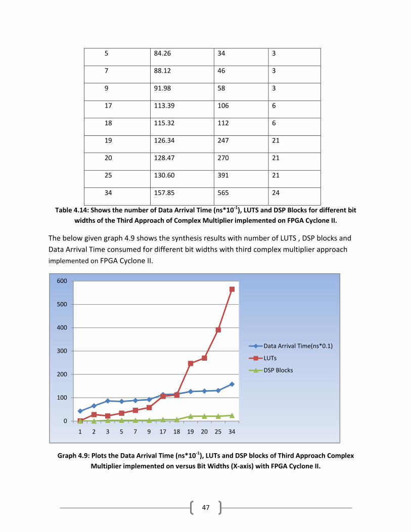
Table 4.14: Shows the number of Data Arrival Time (ns*10-1
), LUTS and DSP Blocks consumed with
respect to Bit Widths of the Third Approach of Complex Multiplier Implementation with FPGA Cyclone
II……………………………………………………………………………………………………………………………………………………………47
Table 4.15: Shows the number of Data Arrival Time (ns*10-1
), LUTS and DSP Blocks consumed with
respect to Bit Widths of the Third Approach of Complex Multiplier Implementation with FPGA Stratix
III…………………………………………………………………………………………………………………………………………………………..48
Table 4.16: Shows the number of Data Arrival Time (ns*10-1
), LUTS and DSP Blocks consumed with
respect to Bit Widths of the Fourth Approach of Complex Multiplier Implementation with FPGA Cyclone
II.……………………………………………………………………………………………………………………………………………………………50
Table 4.17: Shows the number of Data Arrival Time (ns*10-1
), LUTS and DSP Blocks consumed with
respect to Bit Widths of the Fourth Approach of Complex Multiplier Implementation with FPGA Stratix
III……………………………………………………………………………………………………………………………………………………………51
Table 4.18: Number of I/Os, LUTs, DSP blocks, Registers, Memory Bits and Data Arrival Time of a 64 –
point Radix -22 FFT before and after pipelining using registers………………………………………………………………52
Table 4.19: Values which are different from table 4.13………………………………………………………………………….54
Table 4.20: Corresponding Values from table 4.13…………………………………………………………………………………55
16
List of Graphs in the report
Graph 4.1: Number of LUTs consumed for different stages with different Complex Multiplication
approaches with FPGA Cyclone II…………………………………………………………………………………………………………..37
Graph 4.2: Number of LUTs consumed for different stages with different Complex Multiplication
approaches with FPGA Stratix III……………………………………………………………………………………………………………38
Graph 4.3: The Data Arrival Time (in ns) required for different stages with different Complex
Multiplication approaches with FPGA Cyclone II……………………………………………………………………………………39
Graph 4.4: The Data Arrival Time (in ns) required for different stages with different Complex
Multiplication approaches with FPGA Stratix III……………………………………………………………………………………..40
Graph 4.5: Plots the Data Arrival Time (ns*10-1
), LUTs and DSP blocks of First Approach of Complex
Multiplier versus Bit Widths (X-axis) with FPGA Cyclone II…………………………………………………………………….41
Graph 4.6: Plots the Data Arrival Time (ns*10-2
), LUTs and DSP blocks of First Approach of Complex
Multiplier versus Bit Widths (X-axis) with FPGA Stratix III……………………………………………………………………..43
Graph 4.7: Plots the Data Arrival Time (ns*10-1
), LUTs and DSP blocks of Second Approach of Complex
Multiplication versus Bit Widths (X-axis) with FPGA Cyclone II………………………………………………………………44
Graph 4.8: Plots the Data Arrival Time (ns*10-1
), LUTs and DSP blocks of Second Approach of Complex
Multiplication versus Bit Widths (X-axis) with FPGA Stratix III………………………………………………………………..46
Graph 4.9: Plots the Data Arrival Time (ns*10-1
), LUTs and DSP blocks of Third Approach of Complex
Multiplication versus Bit Widths (X-axis) with FPGA Cyclone II………………………………………………………………47
Graph 4.10: Plots the Data Arrival Time (ns*10-1
), LUTs and DSP blocks of Third Approach of Complex
Multiplication versus Bit Widths (X-axis) with FPGA Stratix III………………………………………………………………..48
Graph 4.11: Plots the Data Arrival Time (ns*10-1
), LUTs and DSP blocks of Fourth Approach of Complex
Multiplication versus Bit Widths (X-axis) with FPGA Cyclone II………………………………………………………………50
Graph 4.12: Plots the Data Arrival Time (ns*10-1
), LUTs and DSP blocks of Fourth Approach of Complex
Multiplication versus Bit Widths (X-axis) with FPGA Stratix III………………………………………………………………..52
17
1 Introduction
1.1 DFTs, FFTs and FPGAs
FFT is an algorithm to compute Discrete Fourier Transforms (DFT) and its inverse applications.
FFT has many applications, in fact any field of physical science that uses sinusoidal signals, such
as engineering, physics, applied mathematics, and chemistry. FFT computations play a vital role
in the computations of FPGAs. FPGAs are faster to manufacture and time to market is less1.
FPGAs have simpler design cycle due to the software that handles most of the routing,
placement and timing. With increase in the logic density and other features such as DSP blocks,
Clocking and high-speed serial at lower price points, FPGAs are suitable for any type of design.
A new bit stream can be uploaded remotely into the FPGAs. As there is need for the FPGAs to
run faster and efficient, our project deals with improving the efficiency of the FPGAs by
improving the FFT. The main applications of this project can be in OFDM Transceivers and
Spectrometers.
1.2 DFT Algorithm
DFT has played a key role in the development of Digital Signal Processing concepts.
DFT transform can be defined as
X�k� � ∑ x�n��� ��nk
where k ∈ {0,N-1}
Where WN=℮-2∏j/N
is the Nth
root of unity.
The inverse DFT can be defined as
X�k� � ∑ x�n��� ��-nk
n = {0, N-1}
Where X(k) and x(n) are complex sequences of length N. The computation of DFT and IDFT
requires N2 complex arithmetic operations.
Radix-2 DIF and DIT FFT algorithm definitions:
i) The decimation-in-time (DIT) radix-2 FFT recursively partitions a DFT into two half-length DFTS
of even-indexed and odd-indexed time samples. The outputs of these shorter FFTs are reused
to compute many outputs, thus greatly reducing the total computational cost.
1 http://www.xilinx.com/company/gettingstarted/fpgavsasic.htm
18
ii) The radix-2 decimation-in-frequency (DIF) partitions the DFT computations into even -
indexed and odd-indexed outputs, each of this are computed by shorter-length DFTs of
different combinations of input samples.
1.3 Theme of the Report
After considering all the Pipeline FFT architectures we had concluded to implement Radix-22 DIF
FFT algorithm, as it is one of the best and efficient algorithm to compute DFT. We have
implemented complex multiplier in different ways and after synthesis we have analyzed the
variation on the consumption of the DSP blocks, LUTS and Registers.
1.4 Content of the document
This part describes the contents of the chapters in this report.
Chapter 1 Introduction describes the general introduction of the DFTs and FFTs .It also includes
the main goal of this project and describes the contents in each chapter in this report.
Chapter 2 Basic Pipeline Architectures describes the different pipeline architectures that are
considered for choosing the Architecture for this project. And it also gives the comparison of
different architectures. This chapter also covers why Radix-22 FFT architecture is chosen.
Chapter 3 Radix -22 FFT Architecture describes the architecture and working of Radix-2
2 FFT
architecture. It also contains the calculation of twiddle factor values using the MATLAB.
Chapter 4 FFT Design describes the way in which Radix-22 architecture is implemented in this
project. This chapter discussion includes how the project is carried out from the starting phase
to the end of the project. This chapter also includes the workflow, tools used, methods adopted
for the project and the results obtained.
Chapter 5 Problems faced describes the problems faced during the project.
Chapter 6 Future Work describes the work that can be done in extension to this project and
other things that can be considered to be implemented in the future.
Chapter 7 Summary describes the summary of the complete thesis.
Chapter 8 Bibliography describes the references that have been used in writing this document.
19
2 Basic Pipeline Architectures
2.1 Introduction
This chapter introduces few pipeline architectures and comparison between them.
2.2 Pipeline Architectures
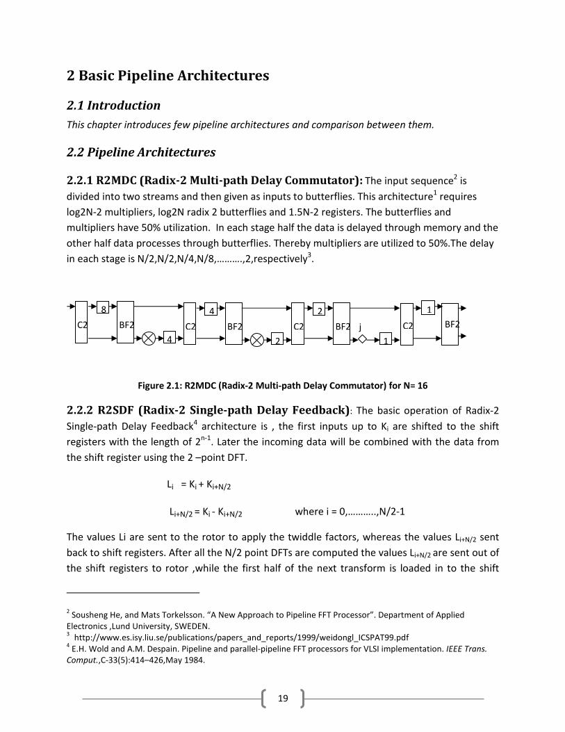
2.2.1 R2MDC (Radix-2 Multi-path Delay Commutator): The input sequence2 is
divided into two streams and then given as inputs to butterflies. This architecture1 requires
log2N-2 multipliers, log2N radix 2 butterflies and 1.5N-2 registers. The butterflies and
multipliers have 50% utilization. In each stage half the data is delayed through memory and the
other half data processes through butterflies. Thereby multipliers are utilized to 50%.The delay
in each stage is N/2,N/2,N/4,N/8,……….,2,respectively3.
Figure 2.1: R2MDC (Radix-2 Multi-path Delay Commutator) for N= 16
2.2.2 R2SDF (Radix-2 Single-path Delay Feedback): The basic operation of Radix-2
Single-path Delay Feedback4 architecture is , the first inputs up to Ki are shifted to the shift
registers with the length of 2n-1
. Later the incoming data will be combined with the data from
the shift register using the 2 –point DFT.
Li = Ki + Ki+N/2
Li+N/2 = Ki - Ki+N/2 where i = 0,………..,N/2-1
The values Li are sent to the rotor to apply the twiddle factors, whereas the values Li+N/2 sent
back to shift registers. After all the N/2 point DFTs are computed the values Li+N/2 are sent out of
the shift registers to rotor ,while the first half of the next transform is loaded in to the shift
2 Sousheng He, and Mats Torkelsson. “A New Approach to Pipeline FFT Processor”. Department of Applied
Electronics ,Lund University, SWEDEN. 3 http://www.es.isy.liu.se/publications/papers_and_reports/1999/weidongl_ICSPAT99.pdf
4 E.H. Wold and A.M. Despain. Pipeline and parallel-pipeline FFT processors for VLSI implementation. IEEE Trans.
Comput.,C-33(5):414–426,May 1984.
C2 BF2
4
8
C2 BF2
2
4
C2 BF2
1
2
j C2
11
BF2
20
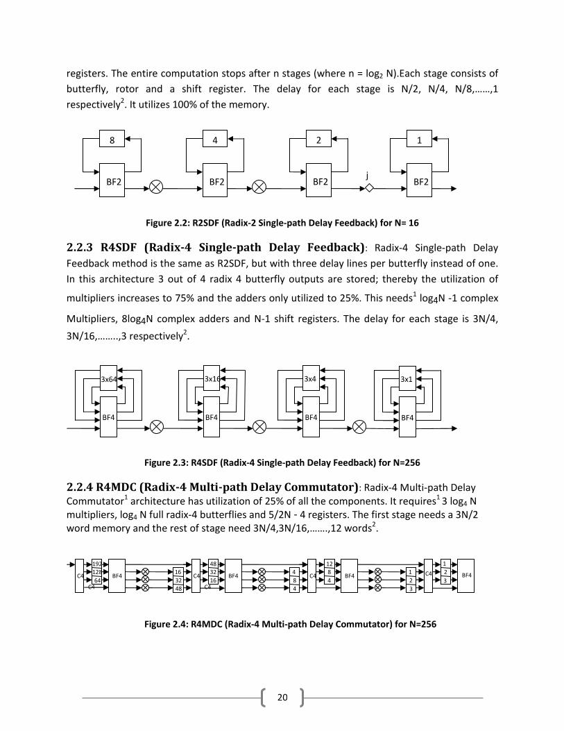
registers. The entire computation stops after n stages (where n = log2 N).Each stage consists of
butterfly, rotor and a shift register. The delay for each stage is N/2, N/4, N/8,……,1
respectively2. It utilizes 100% of the memory.
Figure 2.2: R2SDF (Radix-2 Single-path Delay Feedback) for N= 16
2.2.3 R4SDF (Radix-4 Single-path Delay Feedback): Radix-4 Single-path Delay
Feedback method is the same as R2SDF, but with three delay lines per butterfly instead of one.
In this architecture 3 out of 4 radix 4 butterfly outputs are stored; thereby the utilization of
multipliers increases to 75% and the adders only utilized to 25%. This needs1 log4N -1 complex
Multipliers, 8log4N complex adders and N-1 shift registers. The delay for each stage is 3N/4,
3N/16,……..,3 respectively2.
Figure 2.3: R4SDF (Radix-4 Single-path Delay Feedback) for N=256
2.2.4 R4MDC (Radix-4 Multi-path Delay Commutator): Radix-4 Multi-path Delay
Commutator1 architecture has utilization of 25% of all the components. It requires
1 3 log4 N
multipliers, log4 N full radix-4 butterflies and 5/2N - 4 registers. The first stage needs a 3N/2
word memory and the rest of stage need 3N/4,3N/16,…….,12 words2.
Figure 2.4: R4MDC (Radix-4 Multi-path Delay Commutator) for N=256
192
128 C4 C4 BF4 16
32
48
48
32
16 C4 BF4
4
8
12
8
4 C4 BF4
1
2
4 3 C4
1
2
3 C4
BF4 64
BF4
3x64
BF4
3x16
BF4
3x4
BF4
3x1
BF2
8
BF2
4
BF2
2
BF2
1
j
21
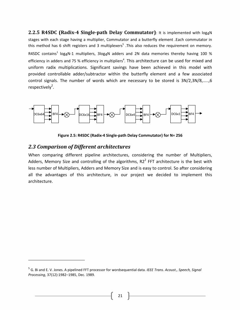
2.2.5 R4SDC (Radix-4 Single-path Delay Commutator): It is implemented with log4N
stages with each stage having a multiplier, Commutator and a butterfly element .Each commutator in
this method has 6 shift registers and 3 multiplexers5 .This also reduces the requirement on memory.
R4SDC contains1 log4N-1 multipliers, 3log4N adders and 2N data memories thereby having 100 %
efficiency in adders and 75 % efficiency in multipliers4. This architecture can be used for mixed and
uniform radix multiplications. Significant savings have been achieved in this model with
provided controllable adder/subtractor within the butterfly element and a few associated
control signals. The number of words which are necessary to be stored is 3N/2,3N/8,…..,6
respectively2.
Figure 2.5: R4SDC (Radix-4 Single-path Delay Commutator) for N= 256
2.3 Comparison of Different architectures
When comparing different pipeline architectures, considering the number of Multipliers,
Adders, Memory Size and controlling of the algorithms, R22 FFT architecture is the best with
less number of Multipliers, Adders and Memory Size and is easy to control. So after considering
all the advantages of this architecture, in our project we decided to implement this
architecture.
5 G. Bi and E. V. Jones. A pipelined FFT processor for wordsequential data. IEEE Trans. Acoust., Speech, Signal
Processing, 37(12):1982–1985, Dec. 1989.
DC6x64 BF4 DC6x16 BF4 DC6x4 BF4 DC6x1 BF4
22
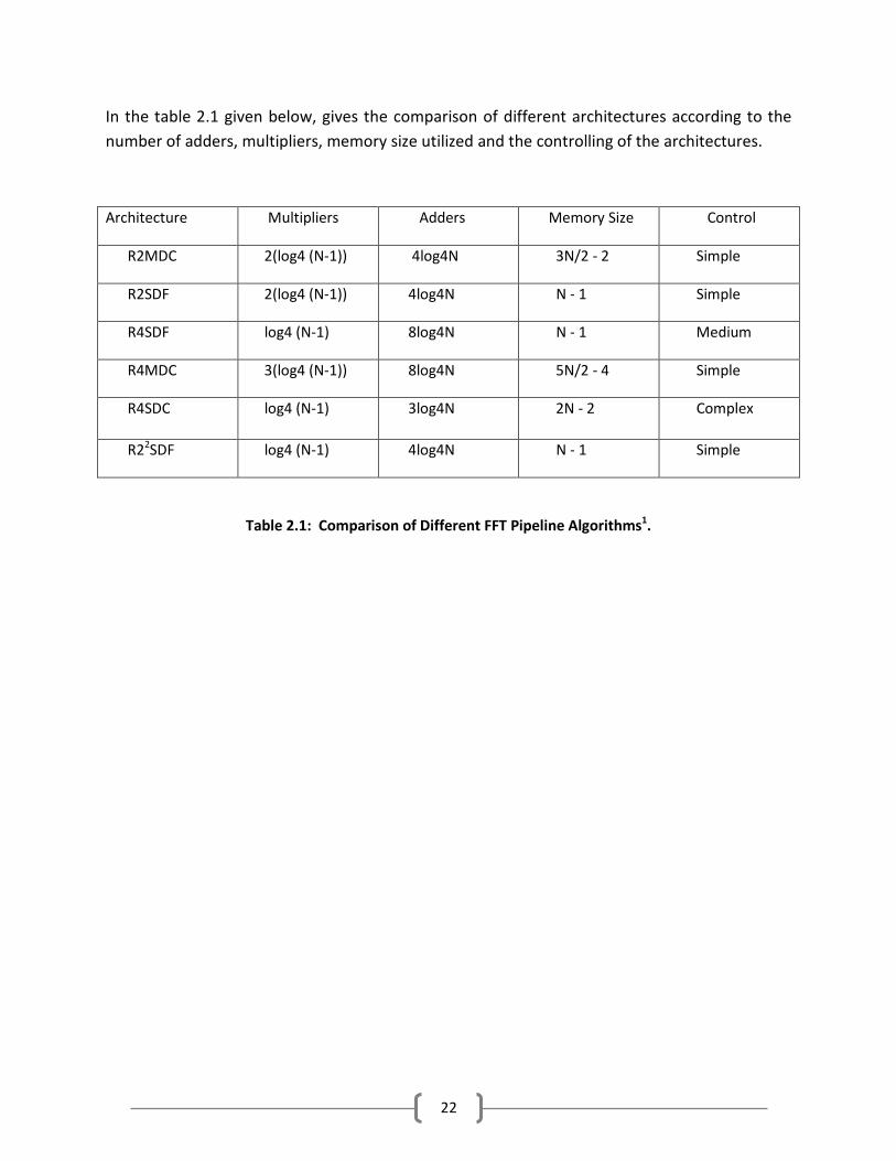
In the table 2.1 given below, gives the comparison of different architectures according to the
number of adders, multipliers, memory size utilized and the controlling of the architectures.
Architecture Multipliers Adders Memory Size Control
R2MDC 2(log4 (N-1)) 4log4N 3N/2 - 2 Simple
R2SDF 2(log4 (N-1)) 4log4N N - 1 Simple
R4SDF log4 (N-1) 8log4N N - 1 Medium
R4MDC 3(log4 (N-1)) 8log4N 5N/2 - 4 Simple
R4SDC log4 (N-1) 3log4N 2N - 2 Complex
R22SDF log4 (N-1) 4log4N N - 1 Simple
Table 2.1: Comparison of Different FFT Pipeline Algorithms1.
23
3 Radix 22 FFT architecture
3.1 Introduction
This chapter discusses the working of the Radix 22 FFT architecture and includes a discussion on
calculation of twiddle factor values in MATLAB.
3.2 Working of R22FFT architecture
As FFT is efficient algorithm to calculate DFT and its inverse.
The basic equation of DFT with size N can be defined as
X�k� � ∑ x�n���� ��nk
where 0 ≤ k < N (3.1)
Here WN represents the primitive root of unity. And considering the first 2 steps of
decomposition in the radix-2 DIF FFT
R22 FFT
1 algorithm can be derived in the following way:
Applying the 3-dimensional linear index map
n= <N/2n1+N/4n2+n3> N
k=<k1 + 2k2 + 4k3>N (3.2)
By using the common factor algorithm (CFA) to the basic DFT equation gives
X (k1 + 2k2 + 4k3)
= � � ∑ x�N/2n₁ � N/4n₂ � n₃�� ₃�� ₂��
�� �
₁��(N/2n1+N/4n2+n3)(k1+2k2+4k3)
= � � ��B ₂��
�� �
₃��N/2
k1)(N/4n2+n3) WN
(N/4n2+n3)(k1)) WN
(N/4n2+n3)( 2k2+4k3) (3.3)
And the butterfly structure has the form
BN/2K1
(N/4n2+n3) = X(N/4n2+n3) + (-1)K1
X(N/4n2+n3 +N/2)
Decomposing the composite twiddle factor in equation (c) gives
WN
(N/4n2+n3)( k1+2k2+4k3)
24
= WN(Nn2k3)
WN
N/4n2( k1+2k2) WN
n3( k1+2k2) WN
4n3k3
= (-j) n2( k1+2k2)
WN
n3( k1+2k2) WN
4n3k3 (3.4)
Substituting the equations (d) in (c) and expanding the summation. After simplifying the
equations we have a set of 4 DFTS of length N/4.
X (k1 + 2k2 + 4k3) = � �H�k , k!, n"��� � #�� WN
n3( k1+2k2) ]WN/4
4n3k3 (3.5)
Where
H (k1,k2,n3) = [x(n3)+(-1)k1
x(n3+N/2)] + (-j)(k1+2k2)
[x(n3+N/4)+(-1)k1
x(n3+3/4N)] (3.6)
x(n3)+(-1)k1
x(n3+N/2)] = BFI (3.7)
x(n3+N/4)+(-1)k1
x(n3+3/4N) = BFI (3.8)
x(n3)+(-1)k1
x(n3+N/2)] + (-j)(k1+2k2)
[x(n3+N/4)+(-1)k1
x(n3+3/4N) = BFII (3.9)
Equation (f) represents the first 2 stages of the butterflies.
After these stages of BFI and BFII, multipliers are required to calculate the decomposed Twiddle
factors (WN
n3( k1+2k2) ) the equation 3.5. Applying the Common Factor Algorithm to the
remaining DFTs of length N/4 , complete Radix 22 FFT algorithm can be obtained .
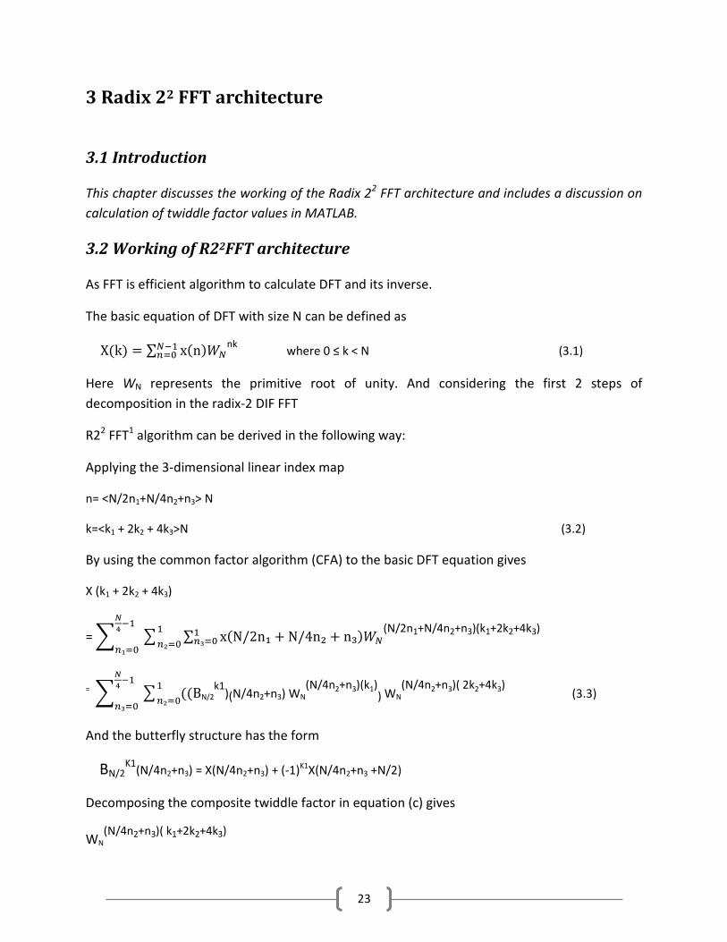
3.3 Working of Butterfly Structures:
On the first N/2 clock cycles the 2-to-1 multiplexers in the first butterfly switch to position zero
and the input data from the left is filled into the shift registers until they are filled and the
butterfly will be in idle stage. On the next N/2 clock cycles the multiplexers turn to position 1
and the first butterfly calculates the 2-point DFT to the input data and the data coming from the
shift registers.
Z1(n) = x(n)+x(n+N/2)
Z1(n+N/2)=x(n)-x(n+N/2) 0 ≤ n < N/2
The output from the first butterfly (Z1(n)) is sent to apply the twiddle factor and Z1(n+N/2) is
sent back to the shift registers that is multiplied in still next N/2 cycles when the first half of the
next frame of time sequences is loaded in. Second Butterfly is similar to that of the first one
except the twiddle factor implementation and distance of butterfly input sequence are N/4. –
25
j(WNN/4
) is used to do the twiddle factor multiplication. Twiddle factor multiplication has been
implemented to do real-imaginary swapping which can be done by a commutator and
controlled add/subtract operations. Synchronizing counter is used to control the add/subtract
operations and the logic gate. Further processing repeats this pattern with the distance of the
input data decreases by half at each consecutive butterfly stages. After N-1 clock cycles th DFT
transform comes from the output in bit reversed order. Due to the pipelined processing of each
stage the next frame of transform can be computed without any pause.
Figure 3.1: BF1
Zr(n+N/2)
Zi(n+N/2)
s
+
+
+
+
Xr(n)
Xi(n)
Xr(n+N/2)
Xi(n+N/2)
0
0
0
1
0
1
1
1
Zr(n)
Zi(n)
26
Figure 3.2 BFII
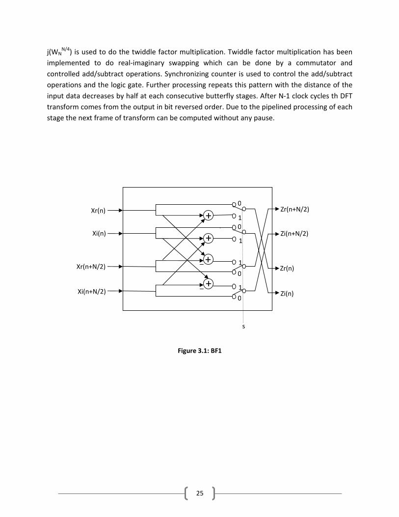
Figure 3.3 R22SDF (256 –Point)
BF2I
128
BF2II
64
s s t
W1(n)
BF2I
32
BF2II
16
s s t
W2(n)
BF2I
8
BF2II
4
s s t
W3(n)
0 1 2 3 4 5 6 7
BF2I
2
s
1
t
BF2II
X(k) s
Zr(n+N/2)
Zi(n+N/2)
s t
Zr(n)
Zi(n)
+
+
+
+
Xr(n)
Xi(n)
Xr(n+N/2)
Xi(n+N/2)
0
0
0
1
0
1
1
1
27
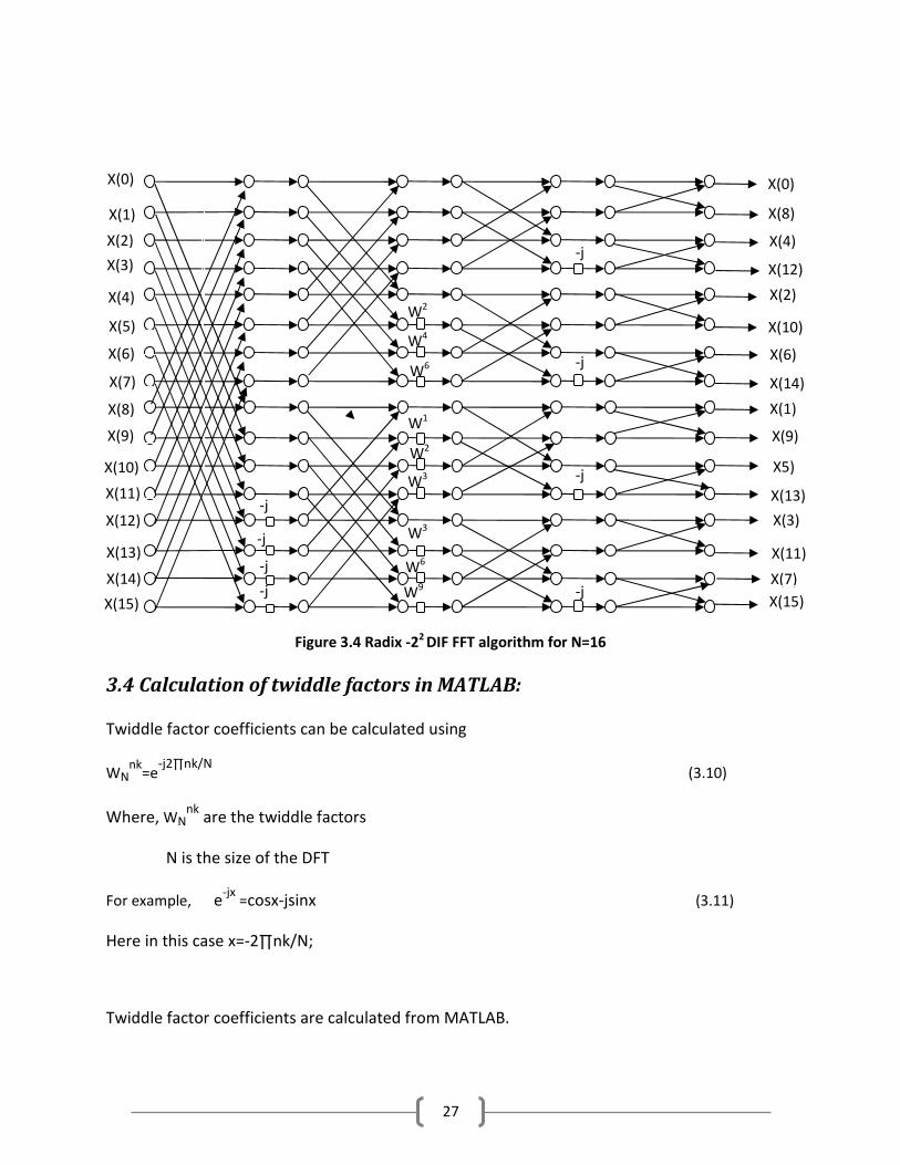
Figure 3.4 Radix -22
DIF FFT algorithm for N=16
3.4 Calculation of twiddle factors in MATLAB:
Twiddle factor coefficients can be calculated using
WNnk
=e-j2∏nk/N
(3.10)
Where, WNnk
are the twiddle factors
N is the size of the DFT
For example, e-jx
=cosx-jsinx (3.11)
Here in this case x=-2∏nk/N;
Twiddle factor coefficients are calculated from MATLAB.
X(15)
-j
-j
-j
-j
W2
-j
-j
-j
-j
W4
W6
W1
W2
W3
W3
X(0)
X(1)
X(2)
X(3)
X(4)
X(5)
X(6)
X(7)
X(8)
X(9)
X(10)
X(11)
X(12)
X(13)
X(14)
X(0)
X(8)
X(4)
X(12)
X(2)
X(10)
X(6)
X(14)
X(1)
X(9)
X5)
X(13)
X(3)
X(11)
X(7)
X(15)
W6
W9
28
From the figure 3.4, the twiddle factor values are W0*area
, W1*area
, W2*area
…….WN/4-1*area
They repeat 4 times and area =0 for first N/4 cycles, area=2 for second N/4 values, area=1 for
third N/4 values and area=3 for last N/4 values.
From the figure 3.3 if we consider for 64-Point there are 2 stages that need twiddle factor
values. Here in the equations 3.13, 3.14 we have used variable “s” which represents the stage.
Index is the value of nk from equation 3.10
The value of index was calculated by using the values of area, stage and mul.
mul is the variable that is used to calculate the index
mul= N/g (3.12)
Variable g is used to calculate the index.
g=N/ (2^ (2*s)) (3.13)
Finally index is calculated by equation
index =(mod(i,(g/4))) * mul * area. (3.14)
Real values of the twiddle factors are calculated by using the cosine function.
Real values = cos (2*∏*index/N). (3.15)
Imaginary values are calculated by using the –sine function.
Imaginary values = =-sin (2*∏*index/N). (3.16)
The real and imaginary values are written into a file using MATLAB.
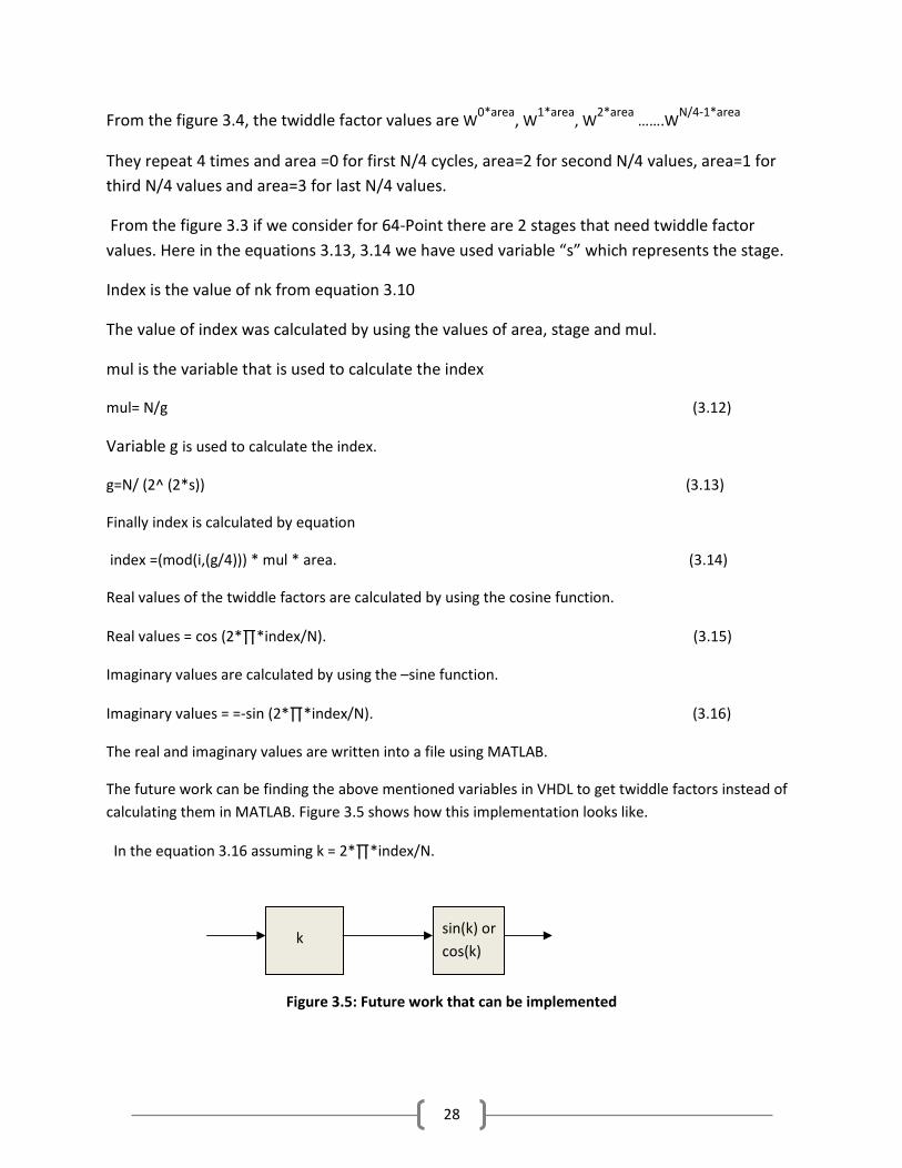
The future work can be finding the above mentioned variables in VHDL to get twiddle factors instead of
calculating them in MATLAB. Figure 3.5 shows how this implementation looks like.
In the equation 3.16 assuming k = 2*∏*index/N.
Figure 3.5: Future work that can be implemented
k sin(k) or
cos(k)
29
4 FFT Design
4.1 Introduction
This chapter describes the implementation of FFT and discusses the different complex multiplier
approaches along with the analysis and presentation of the results.
4.2 Information on the FPGAs used in synthesis.
FPGA’s are finding an extensive application in the field of Digital signal processing. They consist
of DSP blocks, LUT’s, Register’s and I/O’s in order to implement a logic function. In this project
synthesis is performed on two devices with very different features. Cyclone II devices are suited
for multiplier intensive low cost DSP applications and Stratix III devices6 are used for
architecturally advanced, high performance and low power FPGAs. EP2C35F672C from Cyclone
II and EP3SEE50F780C from Stratix III family are selected for implementing the FFT in the
project.
From the Synthesis results obtained, EP2C35F672C from Cyclone II family consists of 475 IO’s,
33216 LE’s and 473 Kbit RAM and 70 DSP blocks (9-bit elements). LE is implemented with a LUT
and a flip-flop (Register).
DSP blocks in this device have embedded multipliers for enhancing performance of the FPGA
thereby reducing the need for other resources. In this Project, they are used for implementing
multipliers.
LUT’s along with Registers are the basic blocks in cyclone II FPGA. LUTs are used during the
implementation of addition operation in the FPGA.
Register is a group of flip flop used to latch and store data. In this project they are used for
introducing pipelining and also for implementing shift registers.
From the synthesis results obtained, EP3SEE50F780C from Stratix III family consists of 488 IO’s,
38000 LE’s and 5328 Kbit RAM and 384 DSP blocks (18-bit elements or 18x18 multipliers). LE is
implemented with a LUT and a flip-flop (Register).
DSP blocks7 of Stratix III devices consists of dedicated elements for performing multiplication,
addition, subtraction, accumulation, summation, and dynamic shift operations and are ideally
suited for complex systems which require a large number of mathematical computations.
“Stratix DSP blocks8 are more than simple multipliers; each DSP has configuration capabilities to
6 http://www.altera.com/products/devices/stratix-fpgas/stratix/stratix/features/stx-dsp.html
7 http://www.altera.com/literature/hb/stx3/stx3_siii51005.pdf
8 http://www.altera.com/literature/wp/wpstxvrtxII.pdf
30
perform up to four 18x18-signed multiplication or two 18x18 multiply-and-accumulate (MAC)
operations at 278 MHz”
LUTs in this device are used during the implementation of addition operation in the FPGA.
Registers in this device are used for introducing pipelining and also for implementing shift
registers.
4.3 Complete flow of the project
We have started with implementing all the blocks in VHDL .Each individual blocks have been
combined together and working of the complete architecture block is tested .After
implementing all the individual blocks, pipelining is done by introducing registers to the
architecture, to reduce the critical path and to increase the performance of the FFT. Complex
Multiplier is implemented in different ways to figure out the number of DSP blocks and LUTs
that are consumed for each approach.
4.3.1 Implementation of Complex Multiplier block and Stage.
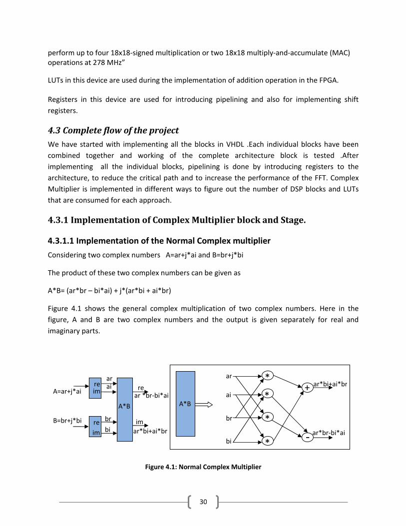
4.3.1.1 Implementation of the Normal Complex multiplier
Considering two complex numbers A=ar+j*ai and B=br+j*bi
The product of these two complex numbers can be given as
A*B= (ar*br – bi*ai) + j*(ar*bi + ai*br)
Figure 4.1 shows the general complex multiplication of two complex numbers. Here in the
figure, A and B are two complex numbers and the output is given separately for real and
imaginary parts.
Figure 4.1: Normal Complex Multiplier
B=br+j*bi
im re
im
re
A*B
ar ai
br
bi
ar *br-bi*ai
ar*bi+ai*br
re
im
A*B
ar
ai
br
bi
*
*
*
*
_+
- ar*br-bi*ai
ar*bi+ai*br A=ar+j*ai
31
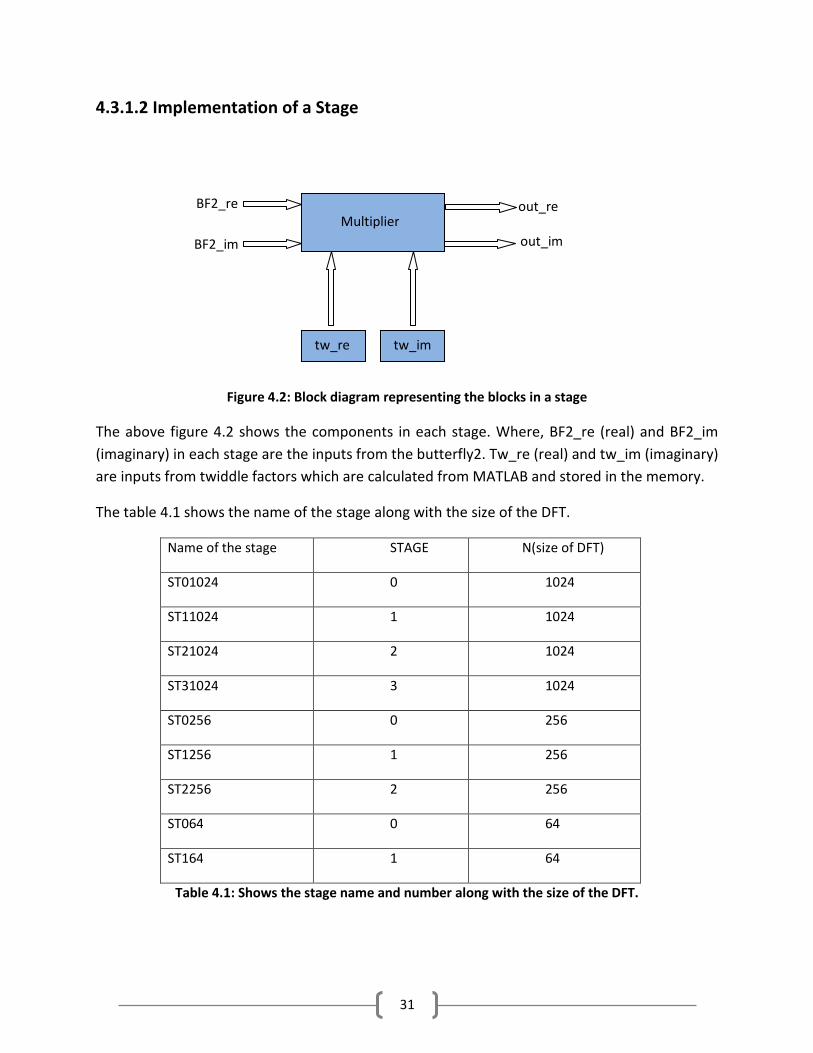
4.3.1.2 Implementation of a Stage
Figure 4.2: Block diagram representing the blocks in a stage
The above figure 4.2 shows the components in each stage. Where, BF2_re (real) and BF2_im
(imaginary) in each stage are the inputs from the butterfly2. Tw_re (real) and tw_im (imaginary)
are inputs from twiddle factors which are calculated from MATLAB and stored in the memory.
The table 4.1 shows the name of the stage along with the size of the DFT.
Name of the stage STAGE N(size of DFT)
ST01024 0 1024
ST11024 1 1024
ST21024 2 1024
ST31024 3 1024
ST0256 0 256
ST1256 1 256
ST2256 2 256
ST064 0 64
ST164 1 64
Table 4.1: Shows the stage name and number along with the size of the DFT.
BF2_im
Multiplier
BF2_re
tw_im tw_re
out_re
out_im
32
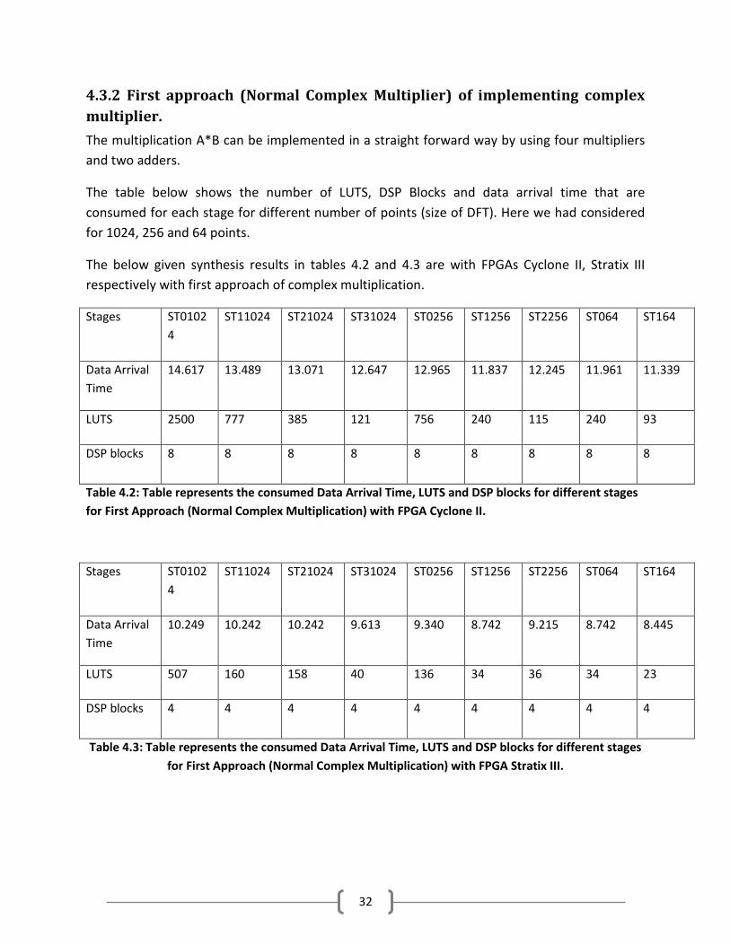
4.3.2 First approach (Normal Complex Multiplier) of implementing complex
multiplier.
The multiplication A*B can be implemented in a straight forward way by using four multipliers
and two adders.
The table below shows the number of LUTS, DSP Blocks and data arrival time that are
consumed for each stage for different number of points (size of DFT). Here we had considered
for 1024, 256 and 64 points.
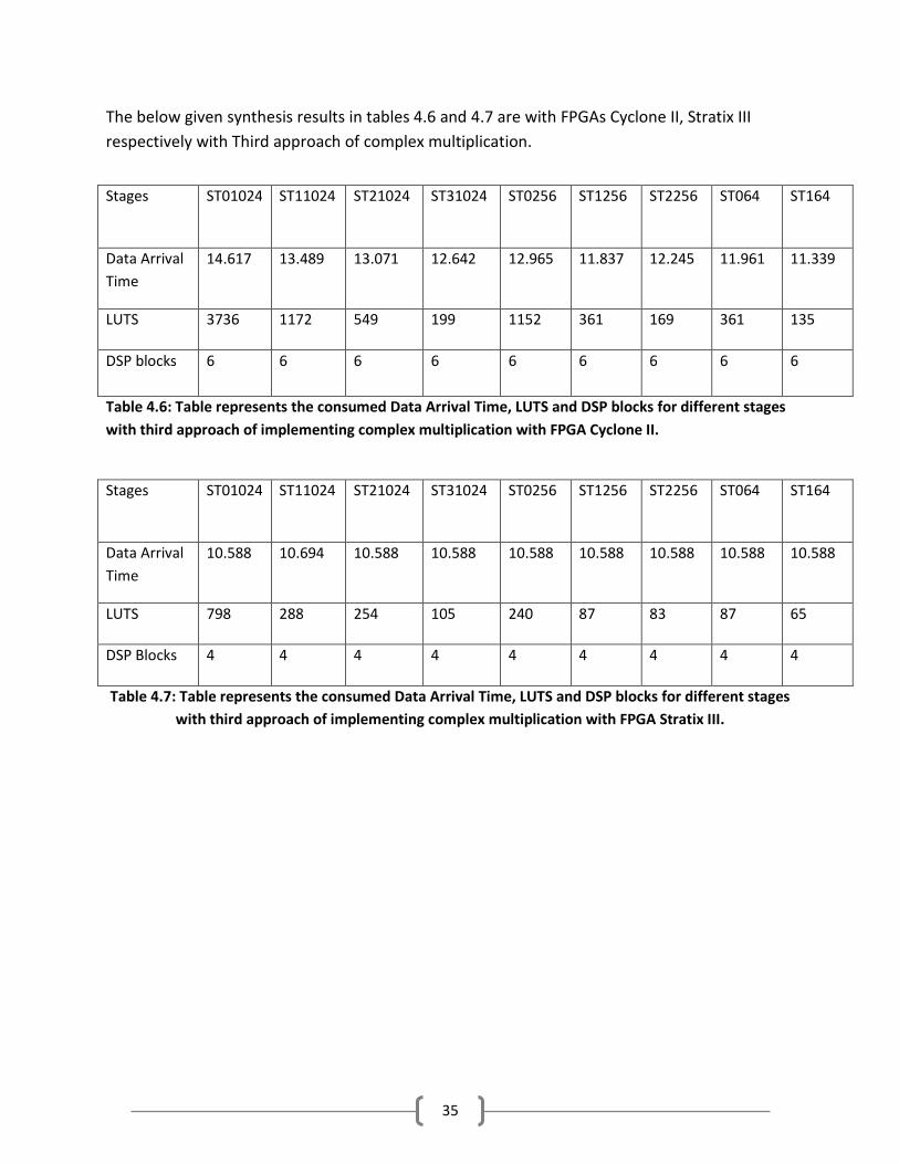
The below given synthesis results in tables 4.2 and 4.3 are with FPGAs Cyclone II, Stratix III
respectively with first approach of complex multiplication.
Stages ST0102
4
ST11024 ST21024 ST31024 ST0256 ST1256 ST2256 ST064 ST164
Data Arrival
Time
14.617 13.489 13.071 12.647 12.965 11.837 12.245 11.961 11.339
LUTS 2500 777 385 121 756 240 115 240 93
DSP blocks 8 8 8 8 8 8 8 8 8
Table 4.2: Table represents the consumed Data Arrival Time, LUTS and DSP blocks for different stages
for First Approach (Normal Complex Multiplication) with FPGA Cyclone II.
Stages ST0102
4
ST11024 ST21024 ST31024 ST0256 ST1256 ST2256 ST064 ST164
Data Arrival
Time
10.249 10.242 10.242 9.613 9.340 8.742 9.215 8.742 8.445
LUTS 507 160 158 40 136 34 36 34 23
DSP blocks 4 4 4 4 4 4 4 4 4
Table 4.3: Table represents the consumed Data Arrival Time, LUTS and DSP blocks for different stages
for First Approach (Normal Complex Multiplication) with FPGA Stratix III.
33
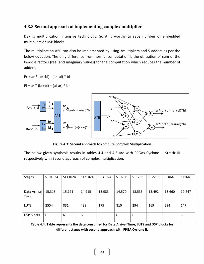
4.3.3 Second approach of implementing complex multiplier
DSP is multiplication intensive technology. So it is worthy to save number of embedded
multipliers or DSP blocks.
The multiplication A*B can also be implemented by using 3multipliers and 5 adders as per the
below equation. The only difference from normal computation is the utilization of sum of the
twiddle factors (real and imaginary values) for the computation which reduces the number of
adders.
Pr = ar * (br+bi) - (ar+ai) * bi
Pi = ar * (br+bi) + (ai-ar) * br
Figure 4.3: Second approach to compute Complex Multiplication
The below given synthesis results in tables 4.4 and 4.5 are with FPGAs Cyclone II, Stratix III
respectively with Second approach of complex multiplication.
Table 4.4: Table represents the data consumed for Data Arrival Time, LUTS and DSP blocks for
different stages with second approach with FPGA Cyclone II.
Stages ST01024 ST11024 ST21024 ST31024 ST0256 ST1256 ST2256 ST064 ST164
Data Arrival
Time
15.315 15.171 14.915 13.983 14.570 13.535 13.492 13.660 12.247
LUTS 2554 831 439 175 810 294 169 294 147
DSP blocks 6 6 6 6 6 6 6 6 6
im re
im
re
A*B
ar ai
br
bi
ar*(br+bi)-(ar+ai)*bi
ar*(br+bi)+(ai-ar)*br
re
im
A*B
ai
br
bi *
_+
-
+
+
-
*
*
*
ar*(br+bi)-(ar+ai)*bi
ar*(br+bi)+(ai-ar)*br
ar
A=ar+jai
B=br+jbi
34
Table 4.5: Table represents the data consumed for Data Arrival Time, LUTS and DSP blocks for
different stages with second approach with FPGA Stratix III.
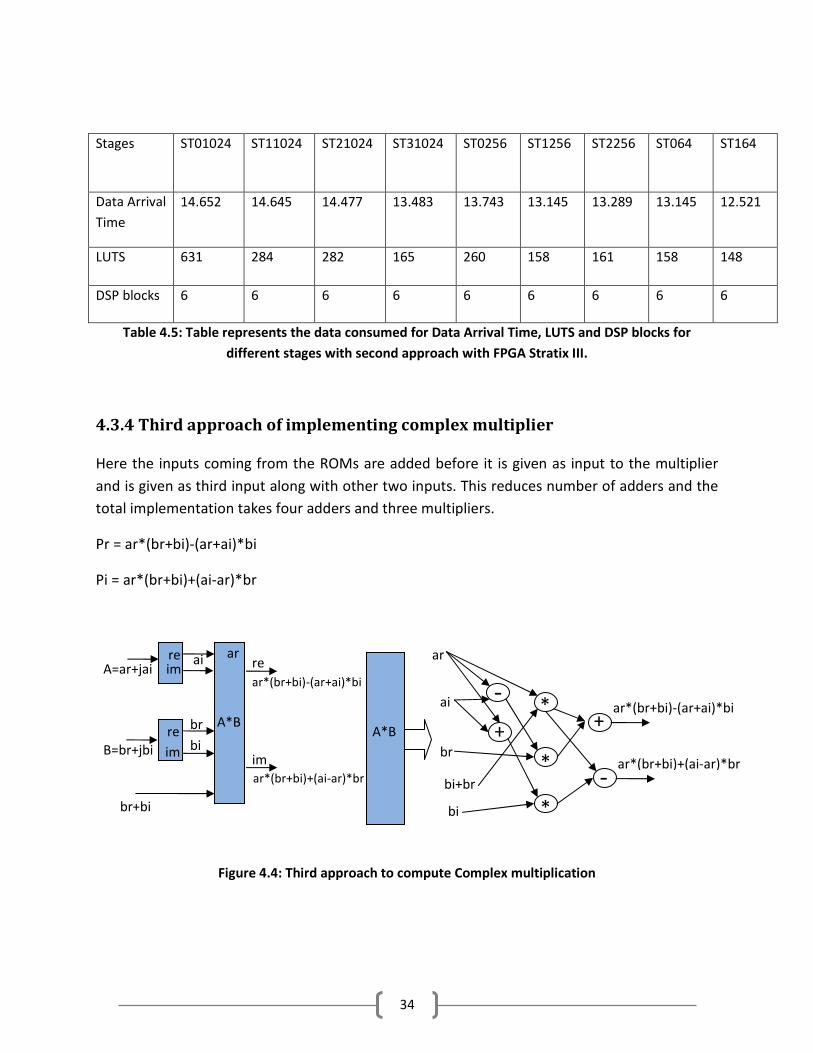
4.3.4 Third approach of implementing complex multiplier
Here the inputs coming from the ROMs are added before it is given as input to the multiplier
and is given as third input along with other two inputs. This reduces number of adders and the
total implementation takes four adders and three multipliers.
Pr = ar*(br+bi)-(ar+ai)*bi
Pi = ar*(br+bi)+(ai-ar)*br
Figure 4.4: Third approach to compute Complex multiplication
Stages ST01024 ST11024 ST21024 ST31024 ST0256 ST1256 ST2256 ST064 ST164
Data Arrival
Time
14.652 14.645 14.477 13.483 13.743 13.145 13.289 13.145 12.521
LUTS 631 284 282 165 260 158 161 158 148
DSP blocks 6 6 6 6 6 6 6 6 6
im re
im
re A*B
ar ai
br
bi
ar*(br+bi)-(ar+ai)*bi
ar*(br+bi)+(ai-ar)*br
re
im
ai
br
bi *
_+
-
+
-
*
*
*
bi+br
A*B
ar*(br+bi)-(ar+ai)*bi
ar*(br+bi)+(ai-ar)*br
ar
B=br+jbi
A=ar+jai
br+bi
35
The below given synthesis results in tables 4.6 and 4.7 are with FPGAs Cyclone II, Stratix III
respectively with Third approach of complex multiplication.
Table 4.6: Table represents the consumed Data Arrival Time, LUTS and DSP blocks for different stages
with third approach of implementing complex multiplication with FPGA Cyclone II.
Table 4.7: Table represents the consumed Data Arrival Time, LUTS and DSP blocks for different stages
with third approach of implementing complex multiplication with FPGA Stratix III.
Stages ST01024 ST11024 ST21024 ST31024 ST0256 ST1256 ST2256 ST064 ST164
Data Arrival
Time
14.617 13.489 13.071 12.642 12.965 11.837 12.245 11.961 11.339
LUTS 3736 1172 549 199 1152 361 169 361 135
DSP blocks 6 6 6 6 6 6 6 6 6
Stages ST01024 ST11024 ST21024 ST31024 ST0256 ST1256 ST2256 ST064 ST164
Data Arrival
Time
10.588 10.694 10.588 10.588 10.588 10.588 10.588 10.588 10.588
LUTS 798 288 254 105 240 87 83 87 65
DSP Blocks 4 4 4 4 4 4 4 4 4
36
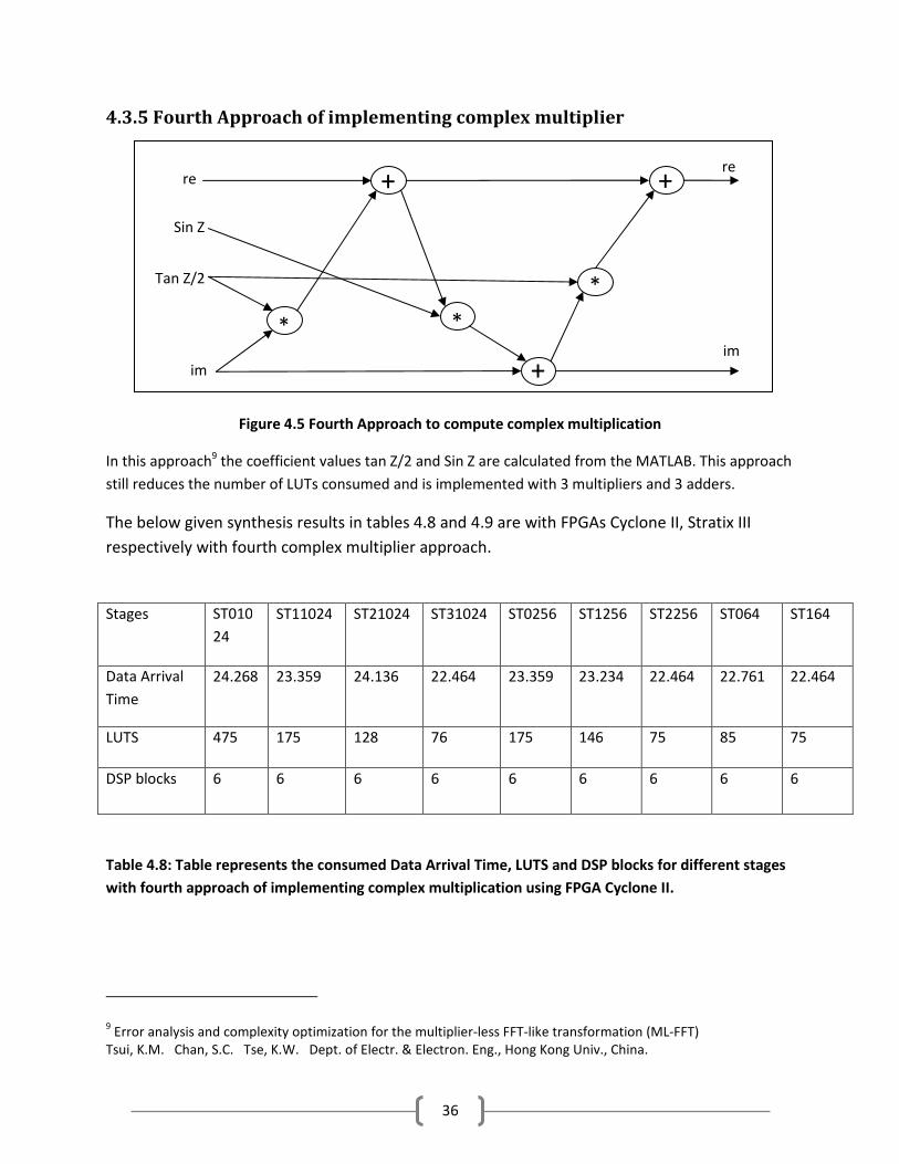
4.3.5 Fourth Approach of implementing complex multiplier
Figure 4.5 Fourth Approach to compute complex multiplication
In this approach9 the coefficient values tan Z/2 and Sin Z are calculated from the MATLAB. This approach
still reduces the number of LUTs consumed and is implemented with 3 multipliers and 3 adders.
The below given synthesis results in tables 4.8 and 4.9 are with FPGAs Cyclone II, Stratix III
respectively with fourth complex multiplier approach.
Table 4.8: Table represents the consumed Data Arrival Time, LUTS and DSP blocks for different stages
with fourth approach of implementing complex multiplication using FPGA Cyclone II.
9 Error analysis and complexity optimization for the multiplier-less FFT-like transformation (ML-FFT)
Tsui, K.M. Chan, S.C. Tse, K.W. Dept. of Electr. & Electron. Eng., Hong Kong Univ., China.
Stages ST010
24
ST11024 ST21024 ST31024 ST0256 ST1256 ST2256 ST064 ST164
Data Arrival
Time
24.268 23.359 24.136 22.464 23.359 23.234 22.464 22.761 22.464
LUTS 475 175 128 76 175 146 75 85 75
DSP blocks 6 6 6 6 6 6 6 6 6
Tan Z/2
im
re +
* *
*
+
+
Sin Z
re
im
37
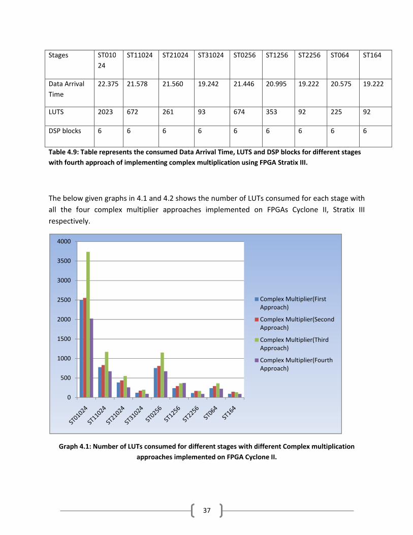
Table 4.9: Table represents the consumed Data Arrival Time, LUTS and DSP blocks for different stages
with fourth approach of implementing complex multiplication using FPGA Stratix III.
The below given graphs in 4.1 and 4.2 shows the number of LUTs consumed for each stage with
all the four complex multiplier approaches implemented on FPGAs Cyclone II, Stratix III
respectively.
Graph 4.1: Number of LUTs consumed for different stages with different Complex multiplication
approaches implemented on FPGA Cyclone II.
0
500
1000
1500
2000
2500
3000
3500
4000
Complex Multiplier(First
Approach)
Complex Multiplier(Second
Approach)
Complex Multiplier(Third
Approach)
Complex Multiplier(Fourth
Approach)
Stages ST010
24
ST11024 ST21024 ST31024 ST0256 ST1256 ST2256 ST064 ST164
Data Arrival
Time
22.375 21.578 21.560 19.242 21.446 20.995 19.222 20.575 19.222
LUTS 2023 672 261 93 674 353 92 225 92
DSP blocks 6 6 6 6 6 6 6 6 6
38
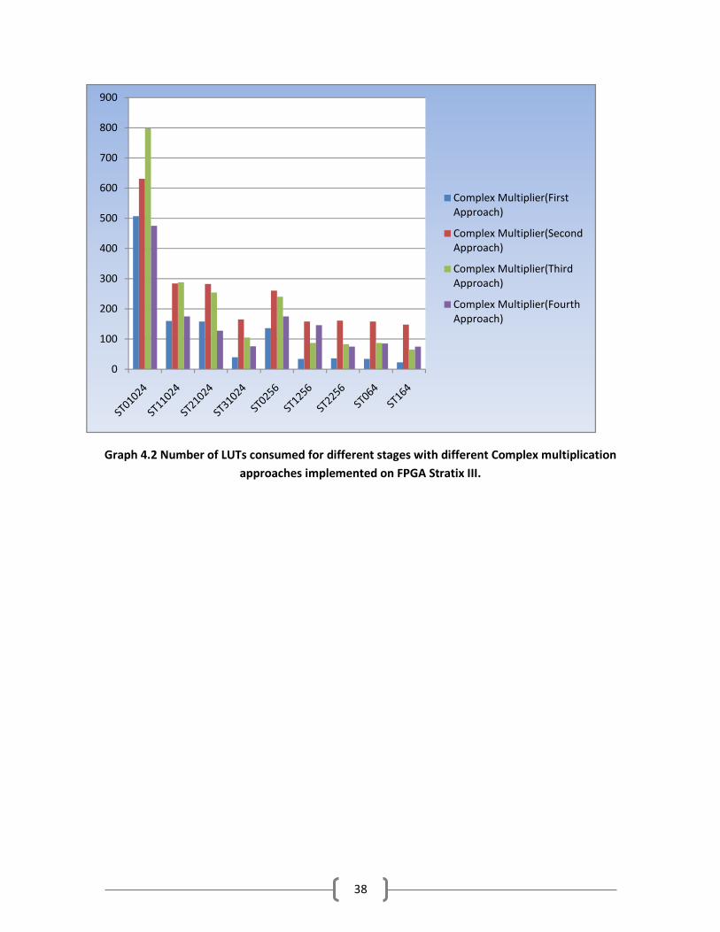
Graph 4.2 Number of LUTs consumed for different stages with different Complex multiplication
approaches implemented on FPGA Stratix III.
0
100
200
300
400
500
600
700
800
900
Complex Multiplier(First
Approach)
Complex Multiplier(Second
Approach)
Complex Multiplier(Third
Approach)
Complex Multiplier(Fourth
Approach)
39
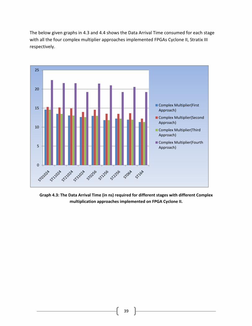
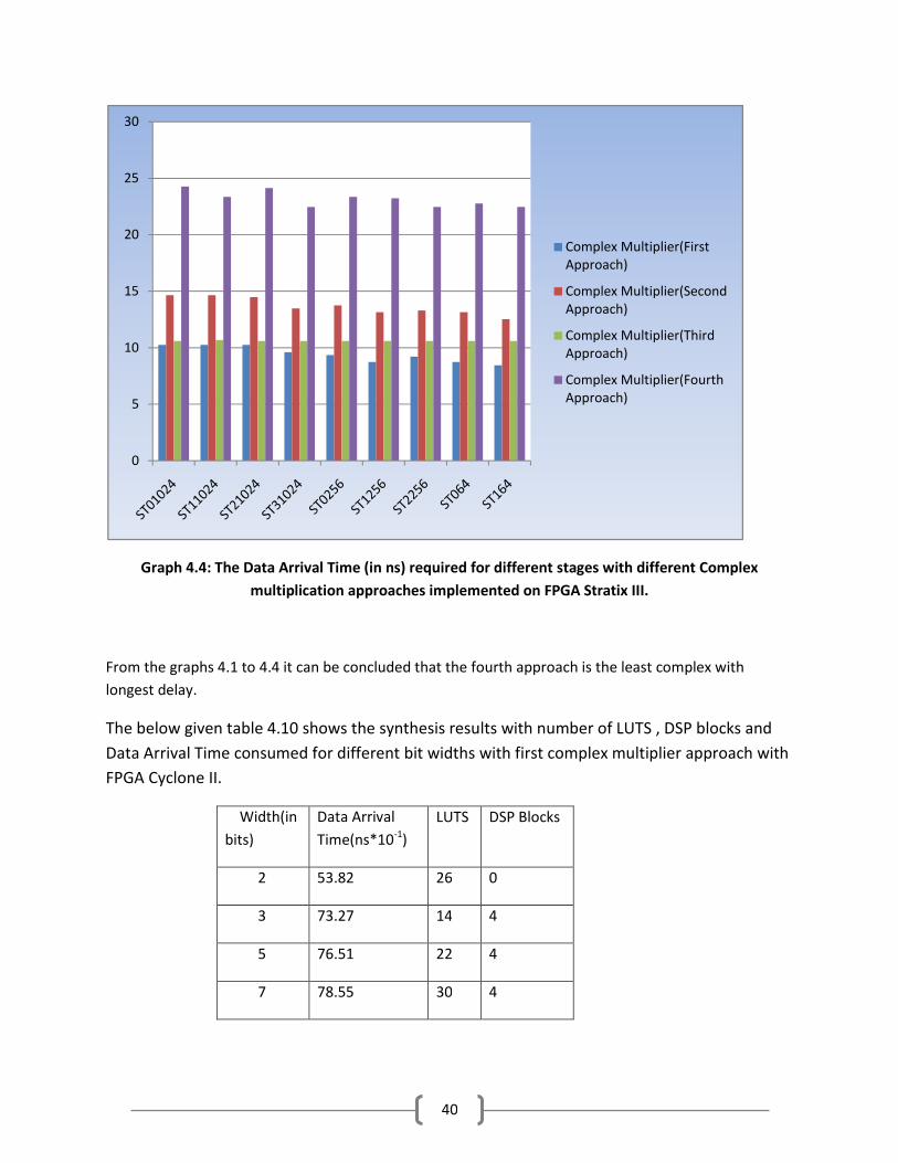
The below given graphs in 4.3 and 4.4 shows the Data Arrival Time consumed for each stage
with all the four complex multiplier approaches implemented FPGAs Cyclone II, Stratix III
respectively.
Graph 4.3: The Data Arrival Time (in ns) required for different stages with different Complex
multiplication approaches implemented on FPGA Cyclone II.
0
5
10
15
20
25
Complex Multiplier(First
Approach)
Complex Multiplier(Second
Approach)
Complex Multiplier(Third
Approach)
Complex Multiplier(Fourth
Approach)
40
Graph 4.4: The Data Arrival Time (in ns) required for different stages with different Complex
multiplication approaches implemented on FPGA Stratix III.
From the graphs 4.1 to 4.4 it can be concluded that the fourth approach is the least complex with
longest delay.
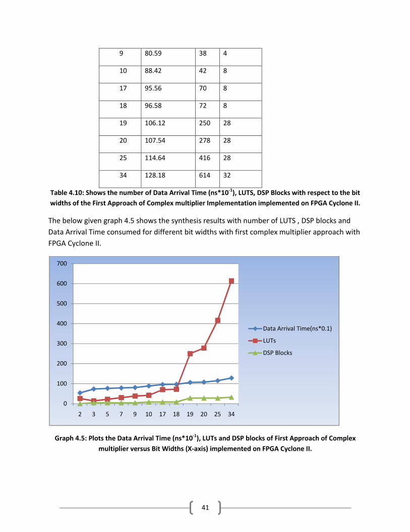
The below given table 4.10 shows the synthesis results with number of LUTS , DSP blocks and
Data Arrival Time consumed for different bit widths with first complex multiplier approach with
FPGA Cyclone II.
Width(in
bits)
Data Arrival
Time(ns*10-1
)
LUTS DSP Blocks
2 53.82 26 0
3 73.27 14 4
5 76.51 22 4
7 78.55 30 4
0
5
10
15
20
25
30
Complex Multiplier(First
Approach)
Complex Multiplier(Second
Approach)
Complex Multiplier(Third
Approach)
Complex Multiplier(Fourth
Approach)
41
9 80.59 38 4
10 88.42 42 8
17 95.56 70 8
18 96.58 72 8
19 106.12 250 28
20 107.54 278 28
25 114.64 416 28
34 128.18 614 32
Table 4.10: Shows the number of Data Arrival Time (ns*10-1
), LUTS, DSP Blocks with respect to the bit
widths of the First Approach of Complex multiplier Implementation implemented on FPGA Cyclone II.
The below given graph 4.5 shows the synthesis results with number of LUTS , DSP blocks and
Data Arrival Time consumed for different bit widths with first complex multiplier approach with
FPGA Cyclone II.
Graph 4.5: Plots the Data Arrival Time (ns*10-1
), LUTs and DSP blocks of First Approach of Complex
multiplier versus Bit Widths (X-axis) implemented on FPGA Cyclone II.
0
100
200
300
400
500
600
700
2 3 5 7 9 10 17 18 19 20 25 34
Data Arrival Time(ns*0.1)
LUTs
DSP Blocks
42
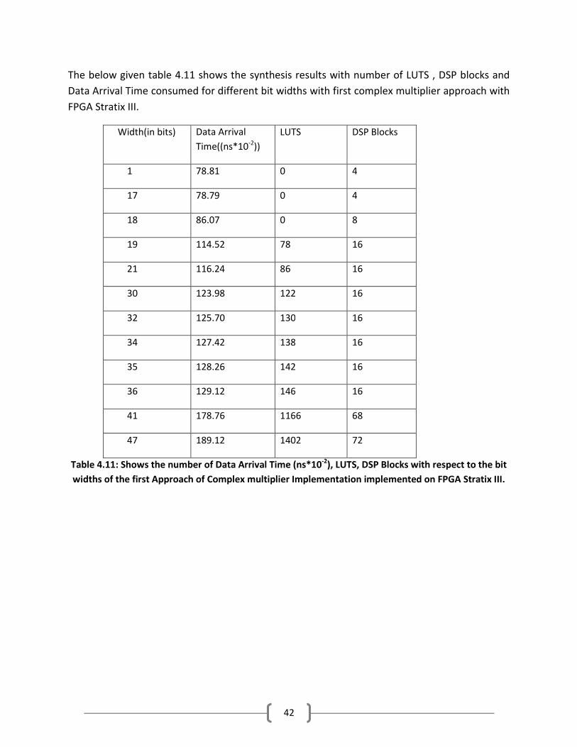
The below given table 4.11 shows the synthesis results with number of LUTS , DSP blocks and
Data Arrival Time consumed for different bit widths with first complex multiplier approach with
FPGA Stratix III.
Width(in bits) Data Arrival
Time((ns*10-2
))
LUTS DSP Blocks
1 78.81 0 4
17 78.79 0 4
18 86.07 0 8
19 114.52 78 16
21 116.24 86 16
30 123.98 122 16
32 125.70 130 16
34 127.42 138 16
35 128.26 142 16
36 129.12 146 16
41 178.76 1166 68
47 189.12 1402 72
Table 4.11: Shows the number of Data Arrival Time (ns*10-2
), LUTS, DSP Blocks with respect to the bit
widths of the first Approach of Complex multiplier Implementation implemented on FPGA Stratix III.
43
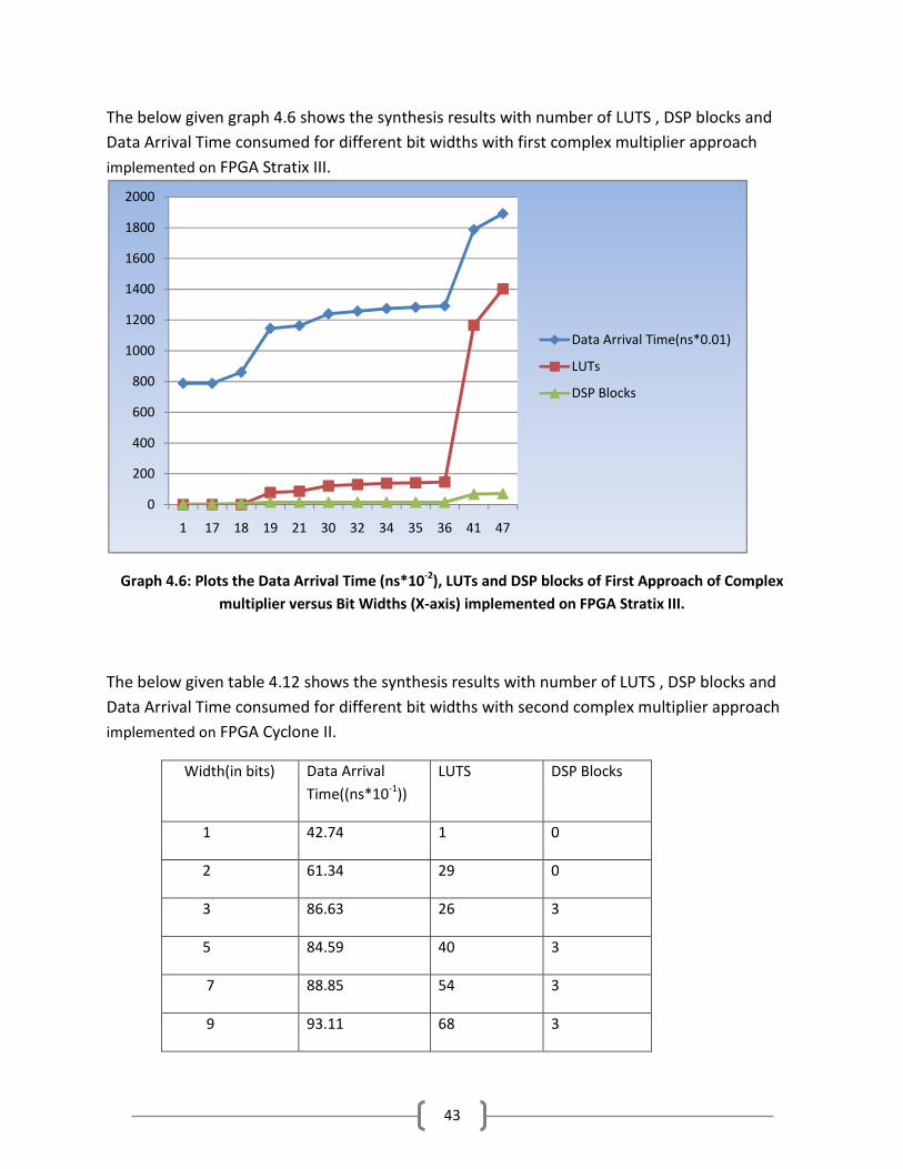
The below given graph 4.6 shows the synthesis results with number of LUTS , DSP blocks and
Data Arrival Time consumed for different bit widths with first complex multiplier approach
implemented on FPGA Stratix III.
Graph 4.6: Plots the Data Arrival Time (ns*10-2
), LUTs and DSP blocks of First Approach of Complex
multiplier versus Bit Widths (X-axis) implemented on FPGA Stratix III.
The below given table 4.12 shows the synthesis results with number of LUTS , DSP blocks and
Data Arrival Time consumed for different bit widths with second complex multiplier approach
implemented on FPGA Cyclone II.
Width(in bits) Data Arrival
Time((ns*10-1
))
LUTS DSP Blocks
1 42.74 1 0
2 61.34 29 0
3 86.63 26 3
5 84.59 40 3
7 88.85 54 3
9 93.11 68 3
0
200
400
600
800
1000
1200
1400
1600
1800
2000
1 17 18 19 21 30 32 34 35 36 41 47
Data Arrival Time(ns*0.01)
LUTs
DSP Blocks
44
17 113.36 124 6
18 115.49 131 6
19 125.96 267 21
20 128.09 289 21
25 138.74 399 21
34 157.91 600 24
Table 4.12: Shows the number of Data Arrival Time (ns*10-1
), LUTS and DSP Blocks consumed with
respect to Bit Widths of the Second Approach of Complex multiplier implemented on FPGA Cyclone II.
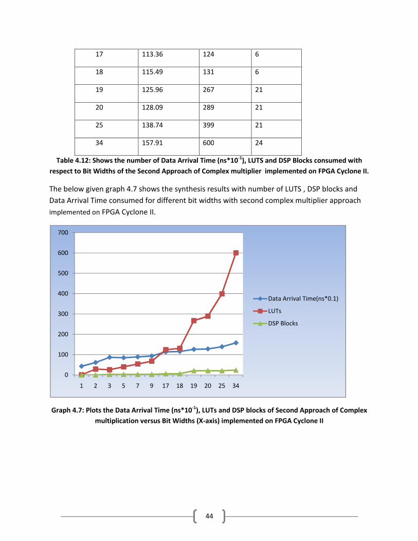
The below given graph 4.7 shows the synthesis results with number of LUTS , DSP blocks and
Data Arrival Time consumed for different bit widths with second complex multiplier approach
implemented on FPGA Cyclone II.
Graph 4.7: Plots the Data Arrival Time (ns*10-1
), LUTs and DSP blocks of Second Approach of Complex
multiplication versus Bit Widths (X-axis) implemented on FPGA Cyclone II
0
100
200
300
400
500
600
700
1 2 3 5 7 9 17 18 19 20 25 34
Data Arrival Time(ns*0.1)
LUTs
DSP Blocks
45
The below given table 4.13 shows the synthesis results with number of LUTS , DSP blocks and
Data Arrival Time consumed for different bit widths with second complex multiplier approach
implemented on FPGA Stratix III.
Table 4.13: Shows the number of Data Arrival Time (ns*10-1
), LUTS and DSP Blocks consumed with
respect to the Bit widths of the Second Approach of Complex multiplier implemented on FPGA Stratix
III.
Width(in bits) Data Arrival
Time(ns*10-1
)
LUTS DSP Blocks
5 110.44 42 3
7 112.16 56 3
9 113.88 68 3
17 122.82 124 6
18 124.11 131 6
19 138.04 138 12
20 139.33 145 12
25 145.78 180 12
34 157.39 243 12
35 158.68 250 12
36 159.97 257 12
37 202.97 894 51
46
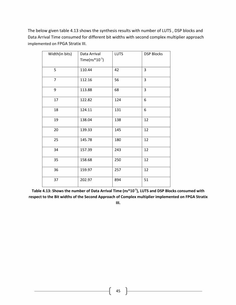
The below given graph 4.8 shows the synthesis results with number of LUTS , DSP blocks and
Data Arrival Time consumed for different bit widths with second complex multiplier approach
implemented on FPGA Stratix III.
Graph 4.8: Plots the Data Arrival Time (ns*10-1
), LUTs and DSP blocks of Second Approach of Complex
multiplication versus Bit Widths (X-axis) implemented on FPGA Stratix III.
The below given table 4.14 shows the synthesis results with number of LUTS , DSP blocks and
Data Arrival Time consumed for different bit widths with third complex multiplier approach
implemented on FPGA Cyclone II.
Width(in bits) Data Arrival
Time(ns*10-1
)
LUTS DSP Blocks
1 42.74 1 0
2 65.24 28 0
3 86.30 22 3
0
100
200
300
400
500
600
700
800
900
1000
5 7 9 17 18 19 20 25 34 35 36 37
Data Arrival Time(ns*0.1)
LUTs
DSP Blocks
47
5 84.26 34 3
7 88.12 46 3
9 91.98 58 3
17 113.39 106 6
18 115.32 112 6
19 126.34 247 21
20 128.47 270 21
25 130.60 391 21
34 157.85 565 24
Table 4.14: Shows the number of Data Arrival Time (ns*10-1
), LUTS and DSP Blocks for different bit
widths of the Third Approach of Complex Multiplier implemented on FPGA Cyclone II.
The below given graph 4.9 shows the synthesis results with number of LUTS , DSP blocks and
Data Arrival Time consumed for different bit widths with third complex multiplier approach
implemented on FPGA Cyclone II.
Graph 4.9: Plots the Data Arrival Time (ns*10-1
), LUTs and DSP blocks of Third Approach Complex
Multiplier implemented on versus Bit Widths (X-axis) with FPGA Cyclone II.
0
100
200
300
400
500
600
1 2 3 5 7 9 17 18 19 20 25 34
Data Arrival Time(ns*0.1)
LUTs
DSP Blocks
48
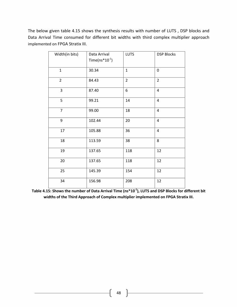
The below given table 4.15 shows the synthesis results with number of LUTS , DSP blocks and
Data Arrival Time consumed for different bit widths with third complex multiplier approach
implemented on FPGA Stratix III.
Width(in bits) Data Arrival
Time(ns*10-1
)
LUTS DSP Blocks
1 30.34 1 0
2 84.43 2 2
3 87.40 6 4
5 99.21 14 4
7 99.00 18 4
9 102.44 20 4
17 105.88 36 4
18 113.59 38 8
19 137.65 118 12
20 137.65 118 12
25 145.39 154 12
34 156.98 208 12
Table 4.15: Shows the number of Data Arrival Time (ns*10-1
), LUTS and DSP Blocks for different bit
widths of the Third Approach of Complex multiplier implemented on FPGA Stratix III.
49
The below given graph 4.10 shows the synthesis results with number of LUTS , DSP blocks and
Data Arrival Time consumed for different bit widths with third complex multiplier approach
implemented on FPGA Stratix III.
Graph 4.10: Plots the Data Arrival Time (ns*10-1
), LUTs and DSP blocks of Third Approach Complex
Multiplier Implementation versus Bit Widths (X-axis) implemented on FPGA Stratix III.
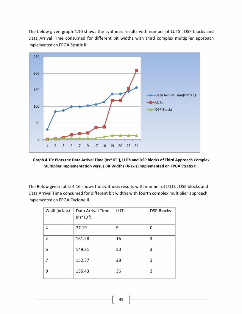
The Below given table 4.16 shows the synthesis results with number of LUTS , DSP blocks and
Data Arrival Time consumed for different bit widths with fourth complex multiplier approach
implemented on FPGA Cyclone II.
0
50
100
150
200
250
1 2 3 5 7 9 17 18 19 20 25 34
Data Arrival Time(ns*0.1)
LUTs
DSP Blocks
Width(in bits) Data Arrival Time
(ns*10-1
)
LUTs DSP Blocks
2 77.19 9 0
3 161.28 16 3
5 149.31 20 3
7 152.37 28 3
9 155.43 36 3
50
Table 4.16: Shows the number of Data Arrival Time (ns*10-1
), LUTS and DSP Blocks for Fourth
Approach Complex Multiplier Implementation versus bit widths implemented on FPGA Cyclone II.
The below given graph 4.11 shows the synthesis results with number of LUTS , DSP blocks and
Data Arrival Time consumed for different bit widths with fourth complex multiplier approach
implemented on FPGA Cyclone II.
Graph 4.11: Plots the Data Arrival Time (ns*10-1
), LUTs and DSP blocks of Fourth Approach Complex
Multiplier Implementation versus Bit Widths (X-axis) implemented on FPGA Cyclone II
0
100
200
300
400
500
600
2 3 5 7 9 10 17 18 19 20 25 34
Data Arrival Time(ns*0.1)
LUTs
DSP Blocks
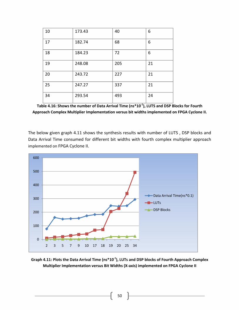
10 173.43 40 6
17 182.74 68 6
18 184.23 72 6
19 248.08 205 21
20 243.72 227 21
25 247.27 337 21
34 293.54 493 24
51
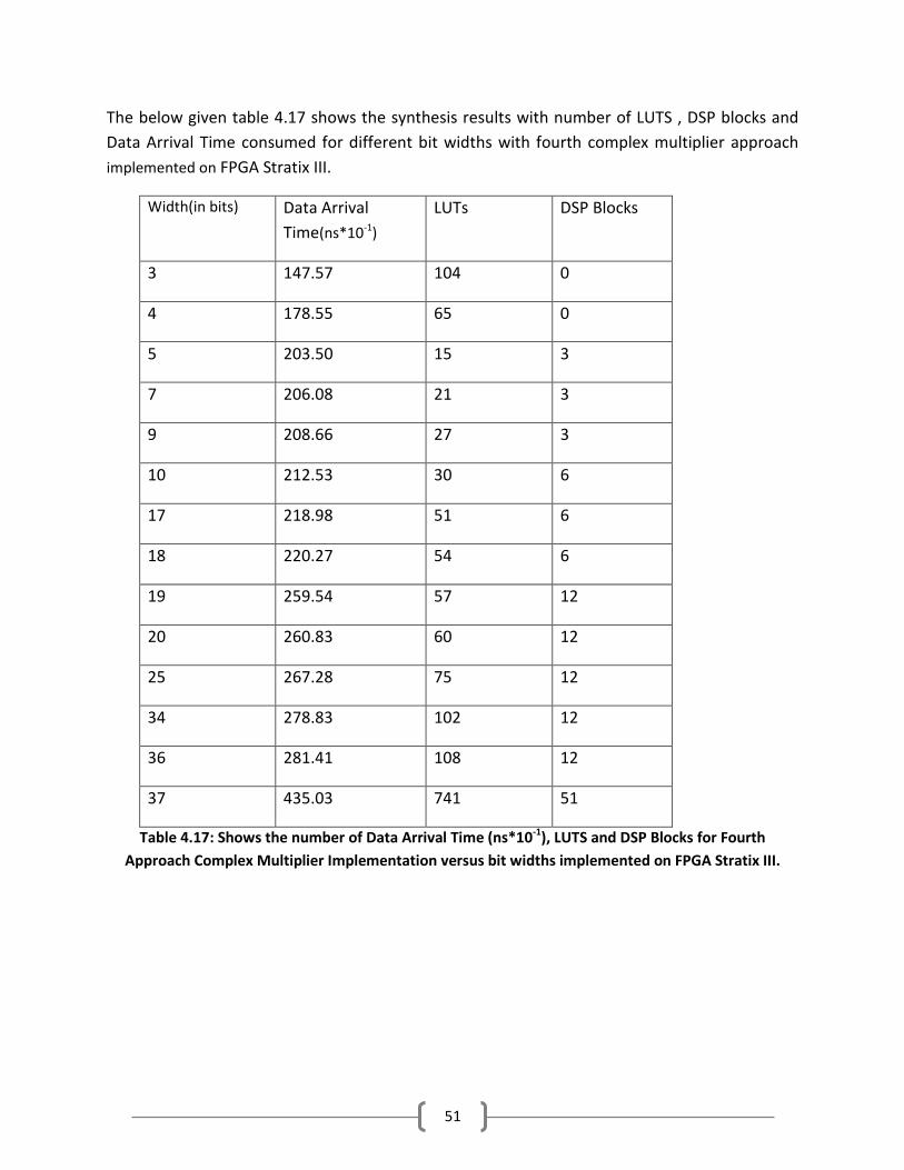
The below given table 4.17 shows the synthesis results with number of LUTS , DSP blocks and
Data Arrival Time consumed for different bit widths with fourth complex multiplier approach
implemented on FPGA Stratix III.
Width(in bits) Data Arrival
Time(ns*10-1
)
LUTs DSP Blocks
3 147.57 104 0
4 178.55 65 0
5 203.50 15 3
7 206.08 21 3
9 208.66 27 3
10 212.53 30 6
17 218.98 51 6
18 220.27 54 6
19 259.54 57 12
20 260.83 60 12
25 267.28 75 12
34 278.83 102 12
36 281.41 108 12
37 435.03 741 51
Table 4.17: Shows the number of Data Arrival Time (ns*10-1
), LUTS and DSP Blocks for Fourth
Approach Complex Multiplier Implementation versus bit widths implemented on FPGA Stratix III.
52
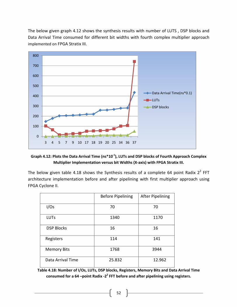
The below given graph 4.12 shows the synthesis results with number of LUTS , DSP blocks and
Data Arrival Time consumed for different bit widths with fourth complex multiplier approach
implemented on FPGA Stratix III.
Graph 4.12: Plots the Data Arrival Time (ns*10-1
), LUTs and DSP blocks of Fourth Approach Complex
Multiplier Implementation versus bit Widths (X-axis) with FPGA Stratix III.
The below given table 4.18 shows the Synthesis results of a complete 64 point Radix 22 FFT
architecture implementation before and after pipelining with first multiplier approach using
FPGA Cyclone II.
Before Pipelining After Pipelining
I/Os 70 70
LUTs 1340 1170
DSP Blocks 16 16
Registers 114 141
Memory Bits 1768 3944
Data Arrival Time 25.832 12.962
Table 4.18: Number of I/Os, LUTs, DSP blocks, Registers, Memory Bits and Data Arrival Time
consumed for a 64 –point Radix -22 FFT before and after pipelining using registers.
0
100
200
300
400
500
600
700
800
3 4 5 7 9 10 17 18 19 20 25 34 36 37
Data Arrival Time(ns*0.1)
LUTs
DSP blocks
53
4.4 Tools and languages used for the implementation of the project.
The project is implemented in VHDL. HDL Designer, MODELSIM and Precision RTL Synthesis are
used for design creation, simulation and synthesis of the design. MATLAB is mainly used in
computing the values of the twiddle factors.
4.5 Testing
Each individual block is tested separately with different input values. After all the individual
blocks were tested successfully, they were implemented together. And values obtained from
the implemented FFT architecture are compared with the values obtained from the MATLAB for
a given input.
4.6 Analysis of the Result
Based on the results from tables 4.2 to 4.17 the following analysis is done.
4.6.1 Analysis of synthesis results (LUTs & DSP blocks consumed by different
complex multiplier approaches with FPGA Cyclone II).
Total number of Look-up-tables (LUTs) used is (2W+1)2 for first approach 1. This equation is
valid for (W= [3, 17]). Total number of Look-up-tables (LUTs) used is 7W+5 for second approach.
This equation is valid for (W= [3, 18]). Total number of Look-up-tables (LUTs) used is 6W+4 for
the third approach. This equation is valid for (W= [3, 18]). They are used during the addition
operations. The number of (LUTs) is 4W for fourth approach and this equation is valid for (W=
[5, 18]). There is a deviation from these equations above the specified widths. For the higher
values of W the unusual increase in LUT consumption still remains mystery.
The number of multiplications is 4 in normal multiplier approach and 3 in other three
approaches. That means each multiplication operator is implemented by 1 DSP block for W= [3,
9] and 2 DSP blocks for W= [10, 18]. For the higher values of W the unusual increase in DSP
block consumption still remains unknown.
4.6.2 Analysis of synthesis results (LUTs & DSP blocks consumed by different
Multiplier approaches with FPGA Stratix III).
Total number of Look-up-tables (LUTs) used in first approach is (2W+1)2 for W=[19,36]; in
second approach, it is 7W+7 for W=[5,7] and 7W+5 for W= [8, 36]; for the third approach, it is
not given by a particular function as the FPGA is implementing some of the adder functionality
in an extra DSP block and in fourth approach it is 3W for W=[5,36]. The LUTs are used during
the addition operations.
54
The number of multiplications is 4 in normal multiplier approach and 3 in other three
approaches.
As mentioned in the section 4.2, In Stratix III, DSP blocks not only do multiplications but they
also do multiplication and accumulation operations. In the first approach, 1 DSP block is used
for each multiplier implementation for W= [1, 17], 2 DSP blocks for W=18 and 4 DSP blocks for
W= [19, 36]. In the second approach, 1 DSP block is used to implement each multiplier for
W=[5,9], 2 DSP blocks are used to implement each multiplier for W= [17, 18] and 4 DSP blocks
for W= [19, 36]. In the third approach, 4 DSP blocks are used to implement three multipliers for
W= [3, 17], 8 DSP blocks for W=18 and 12 DSP blocks for W= [19, 34]. Here, DSP blocks are
involved in implementing addition operations along with multiplications. In the fourth
approach, 1 DSP block is used for each multiplier implementation for W= [5, 17], 2 DSP blocks
for W=18 and 4 DSP blocks for W= [19, 36].
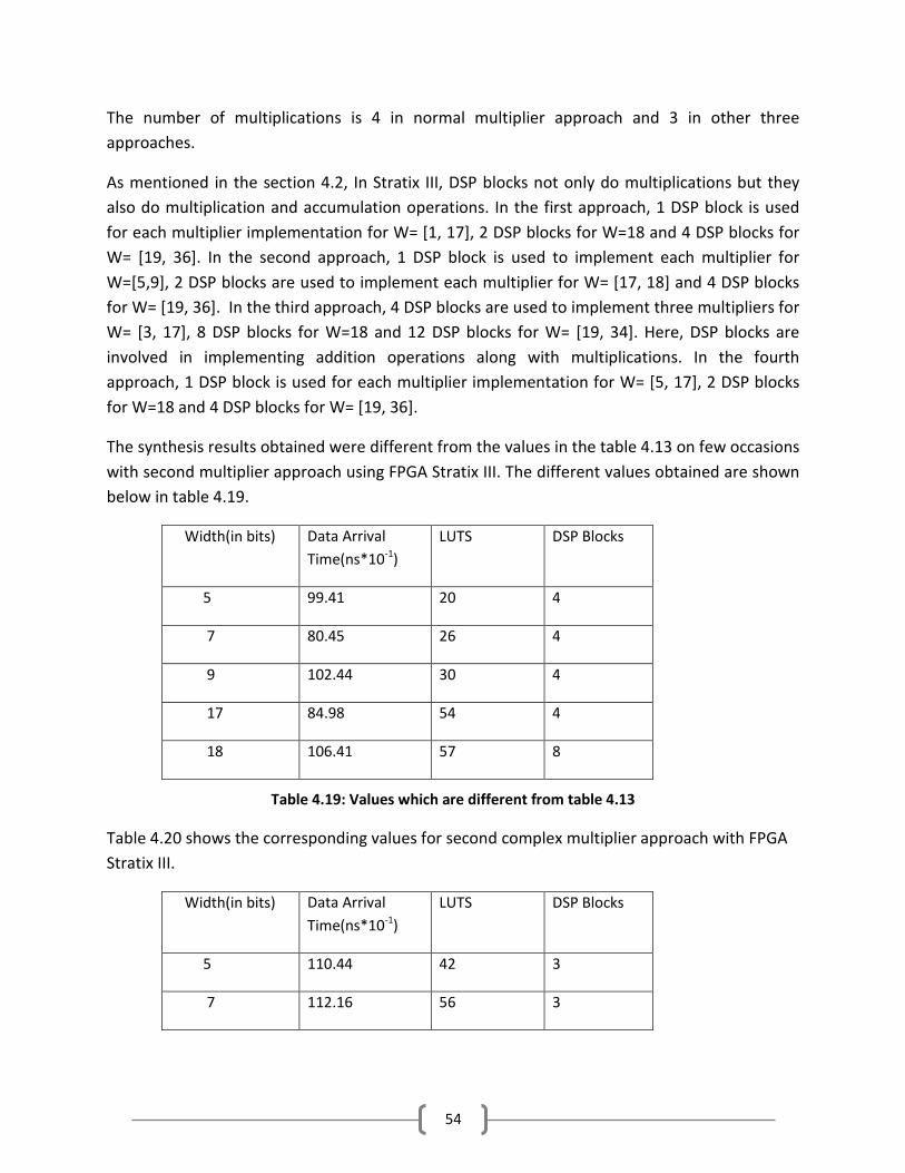
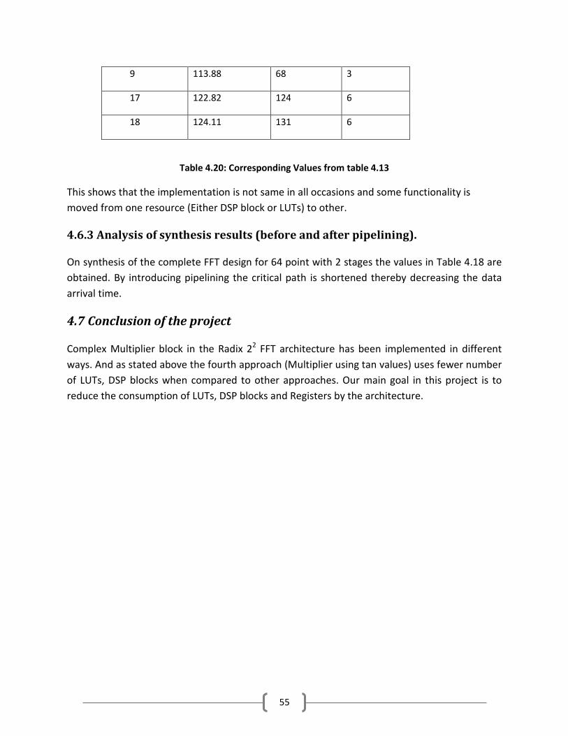
The synthesis results obtained were different from the values in the table 4.13 on few occasions
with second multiplier approach using FPGA Stratix III. The different values obtained are shown
below in table 4.19.
Table 4.19: Values which are different from table 4.13
Table 4.20 shows the corresponding values for second complex multiplier approach with FPGA
Stratix III.
Width(in bits) Data Arrival
Time(ns*10-1
)
LUTS DSP Blocks
5 99.41 20 4
7 80.45 26 4
9 102.44 30 4
17 84.98 54 4
18 106.41 57 8
Width(in bits) Data Arrival
Time(ns*10-1
)
LUTS DSP Blocks
5 110.44 42 3
7 112.16 56 3
55
Table 4.20: Corresponding Values from table 4.13
This shows that the implementation is not same in all occasions and some functionality is
moved from one resource (Either DSP block or LUTs) to other.
4.6.3 Analysis of synthesis results (before and after pipelining).
On synthesis of the complete FFT design for 64 point with 2 stages the values in Table 4.18 are
obtained. By introducing pipelining the critical path is shortened thereby decreasing the data
arrival time.
4.7 Conclusion of the project
Complex Multiplier block in the Radix 22 FFT architecture has been implemented in different
ways. And as stated above the fourth approach (Multiplier using tan values) uses fewer number
of LUTs, DSP blocks when compared to other approaches. Our main goal in this project is to
reduce the consumption of LUTs, DSP blocks and Registers by the architecture.
9 113.88 68 3
17 122.82 124 6
18 124.11 131 6
56
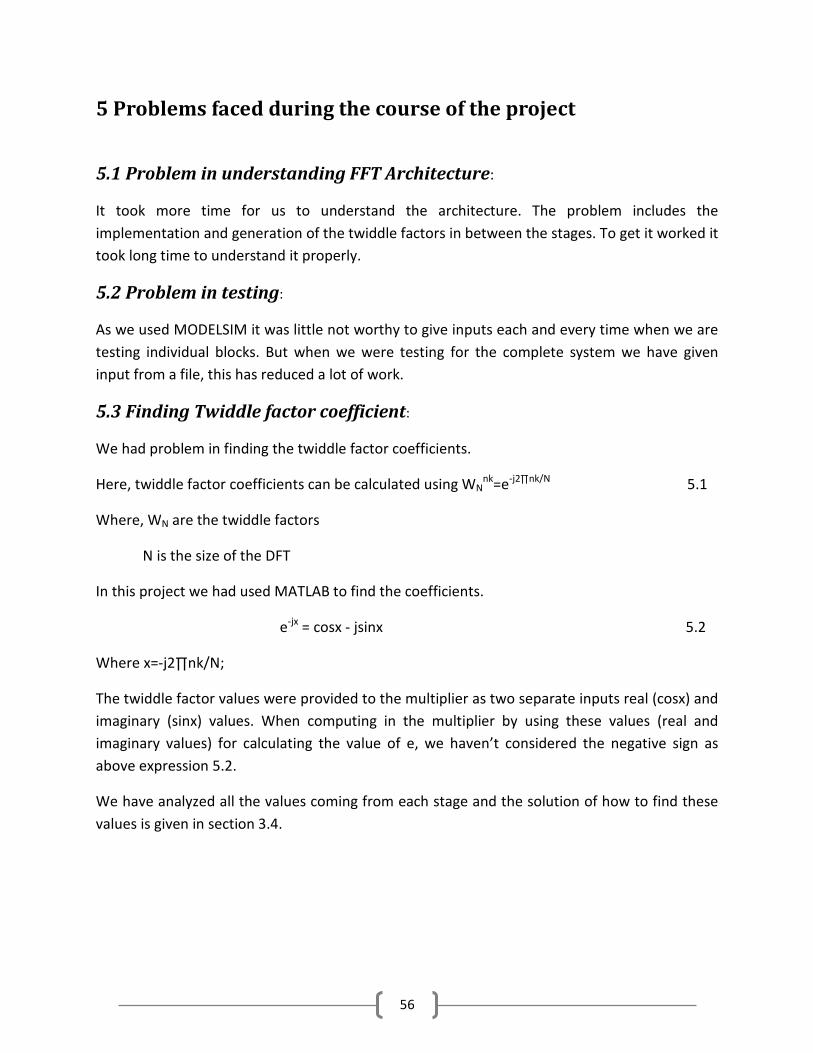
5 Problems faced during the course of the project
5.1 Problem in understanding FFT Architecture:
It took more time for us to understand the architecture. The problem includes the
implementation and generation of the twiddle factors in between the stages. To get it worked it
took long time to understand it properly.
5.2 Problem in testing:
As we used MODELSIM it was little not worthy to give inputs each and every time when we are
testing individual blocks. But when we were testing for the complete system we have given
input from a file, this has reduced a lot of work.
5.3 Finding Twiddle factor coefficient:
We had problem in finding the twiddle factor coefficients.
Here, twiddle factor coefficients can be calculated using WNnk
=e-j2∏nk/N
5.1
Where, WN are the twiddle factors
N is the size of the DFT
In this project we had used MATLAB to find the coefficients.
e-jx
= cosx - jsinx 5.2
Where x=-j2∏nk/N;
The twiddle factor values were provided to the multiplier as two separate inputs real (cosx) and
imaginary (sinx) values. When computing in the multiplier by using these values (real and
imaginary values) for calculating the value of e, we haven’t considered the negative sign as
above expression 5.2.
We have analyzed all the values coming from each stage and the solution of how to find these
values is given in section 3.4.
57
6 Future Work
1) Twiddle factors can be implemented using VHDL to reduce the number of DSP blocks,
LUTS and Registers instead of taking values directly from the MATLAB, the solution and
the equations related to this work are discussed in section 3.4.
2) The Synthesis can be performed for different FPGAs.
3) This architecture can be implemented for higher frequencies.
4) A VHDL generator can be developed for the complete architecture.
5) More detailed analysis of synthesis results should be done. For example sometimes in
table it has implemented with different LUTs and DSP blocks for the same multiplier
approach with same FPGA.
58
7 Summary
Radix -22 Algorithms has been chosen to implement and the different blocks in the architecture
are analyzed and implemented. After implementing the blocks, the complex multiplier
implementation has been done in four different approaches starting from the basic complex
multiplication. Synthesis has been performed for each stage (Multiplier with Twiddle Factors)
and the values of LUTs and DSP Blocks are taken accordingly. Analysis of the synthesis results
has been done and presented in the report.
59
8 Bibliography
1) http://www.xilinx.com/company/gettingstarted/fpgavsasic.htm
2) 2) Sousheng He, and Mats Torkelsson. “A New Approach to Pipeline FFT Processor”. Department
of Applied Electronics ,Lund University, SWEDEN. 3) http://www.es.isy.liu.se/publications/papers_and_reports/1999/weidongl_ICSPAT99.pd
f
4) E.H. Wold and A.M. Despain. Pipeline and parallel-pipeline FFT processors for VLSI
implementation. IEEE Trans. Comput.,C-33(5):414–426,May 1984. 5) G. Bi and E. V. Jones. A pipelined FFT processor for word sequential data. IEEE Trans.
Acoust., Speech, Signal Processing, 37(12):1982–1985, Dec. 1989.
6) http://www.altera.com/products/devices/stratix-fpgas/stratix/stratix/features/stx-
dsp.html 7) http://www.altera.com/literature/hb/stx3/stx3_siii51005.pdf 8) http://www.altera.com/literature/wp/wpstxvrtxII.pdf
9) Error analysis and complexity optimization for the multiplier-less FFT-like transformation
(ML-FFT) Tsui, K.M. Chan, S.C. Tse, K.W. Dept. of Electr. & Electron. Eng., Hong Kong
Univ., China.
På svenska Detta dokument hålls tillgängligt på Internet från publiceringsdatum under förutsättning att inga extra Tillgång till dokumentet innebär tillstånd för var kopior för enskilt bruk och att använda det oförändrat för ickekommersiell forskning och för undervisning. Överföring av upphovsrätten vid en senare tidpunkt kan inte upphäva detta tillstånd. All annan användning av dokumentet kräver upphovsmannens medgivande. För att garantera äktheten, säkerheten och tillgängligheten finns det lösningar av teknisk och administrativ art. Upphovsmannens ideella rätt innefattar rätt att bli nämnd som upphovsman i den omfgod sed kräver vid användning av dokumentet på ovan beskrivna sätt samt skydd mot attdokumentet ändras eller presenteras i sådan form eller i sådant sammanhang som är kränkande för upphovsmannens litterära eller konstnärliga anseende eller egeinformation om Linköping University Electronic Press se förlagets hemsida In English The publishers will keep this document online on the Internet considerable time from the date of publication barring exceptional circumstances. The online availability of the document implies a permanent permission for anyone to read, todownload, to print out single copies for your own use and to use it unchanged for any noncommercial research and educational purpose. Subsequent transfers of copyright cannot revoke this permission. All other uses of the document are conditional on the consent of the copyright owner. The publisher has taken technical and administrative measures to assure authenticity, security and accessibility. According to intellectual property law the author has the rigwork is accessed as described above and to be protected against infringement. For additional information about the Linköping University Electronic Press and its procedures for publication and for assurance of document integrity, please refer to its WWW home page: http://www.ep.liu.se/ © Praneeth Kumar Thangella & Aravind Reddy Gundla
60
Detta dokument hålls tillgängligt på Internet – eller dess framtida ersättare – under en längre tid från publiceringsdatum under förutsättning att inga extra-ordinära omständigheter uppstår.
Tillgång till dokumentet innebär tillstånd för var och en att läsa, ladda ner, skriva ut enstaka för enskilt bruk och att använda det oförändrat för ickekommersiell forskning och för
Överföring av upphovsrätten vid en senare tidpunkt kan inte upphäva detta användning av dokumentet kräver upphovsmannens medgivande. För att säkerheten och tillgängligheten finns det lösningar av teknisk och
Upphovsmannens ideella rätt innefattar rätt att bli nämnd som upphovsman i den omfgod sed kräver vid användning av dokumentet på ovan beskrivna sätt samt skydd mot attdokumentet ändras eller presenteras i sådan form eller i sådant sammanhang som är kränkande
upphovsmannens litterära eller konstnärliga anseende eller egenart. För ytterligare Linköping University Electronic Press se förlagets hemsida http://www.ep.liu.se/
The publishers will keep this document online on the Internet - or its possible replacement the date of publication barring exceptional circumstances.
The online availability of the document implies a permanent permission for anyone to read, todownload, to print out single copies for your own use and to use it unchanged for any
search and educational purpose. Subsequent transfers of copyright cannot permission. All other uses of the document are conditional on the consent of the
The publisher has taken technical and administrative measures to assure and accessibility.
According to intellectual property law the author has the right to be mentioned when his/her accessed as described above and to be protected against infringement. For additional
ing University Electronic Press and its procedures for publication assurance of document integrity, please refer to its WWW home page:
Aravind Reddy Gundla
under en längre tid ordinära omständigheter uppstår.
och en att läsa, ladda ner, skriva ut enstaka för enskilt bruk och att använda det oförändrat för ickekommersiell forskning och för
Överföring av upphovsrätten vid en senare tidpunkt kan inte upphäva detta användning av dokumentet kräver upphovsmannens medgivande. För att säkerheten och tillgängligheten finns det lösningar av teknisk och
Upphovsmannens ideella rätt innefattar rätt att bli nämnd som upphovsman i den omfattning som god sed kräver vid användning av dokumentet på ovan beskrivna sätt samt skydd mot att dokumentet ändras eller presenteras i sådan form eller i sådant sammanhang som är kränkande
nart. För ytterligare http://www.ep.liu.se/
or its possible replacement - for a the date of publication barring exceptional circumstances.
The online availability of the document implies a permanent permission for anyone to read, to download, to print out single copies for your own use and to use it unchanged for any
search and educational purpose. Subsequent transfers of copyright cannot permission. All other uses of the document are conditional on the consent of the
The publisher has taken technical and administrative measures to assure
ht to be mentioned when his/her accessed as described above and to be protected against infringement. For additional
ing University Electronic Press and its procedures for publication assurance of document integrity, please refer to its WWW home page: