Embed Size (px)
Citation preview
COMPOUNDSEMICONDUCTOR
January/February 2006 Volume 12 Number 1
C O N N E C T I N G T H E C O M P O U N D S E M I C O N D U C T O R C O M M U N I T Y
JDSU’s Toby Striteon a strategic shiftin laser diodes p13
OPINION INDUSTRY TECHNOLOGY
Switched onLEDs and GaN lasersmake a splash at theConsumer ElectronicsShow in Vegas. p5
Crowded houseWill the wealth ofsuppliers force down SiCsubstrate prices? p16
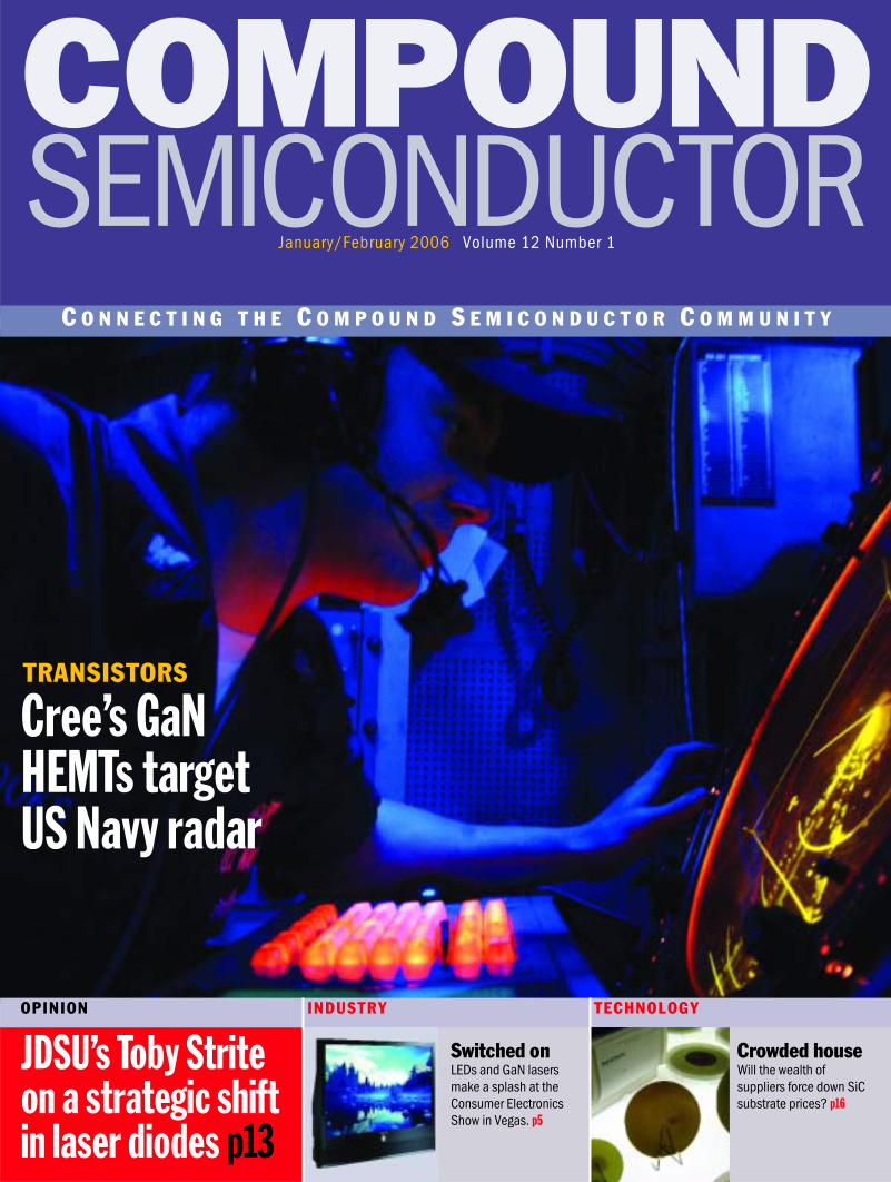
TRANSISTORS
Cree’s GaN HEMTs target US Navy radar
COMPOUNDSEMICONDUCTOR
JANUARY/FEBRUARY 2006V O L U M E 1 2 N U M B E R 1
C O N N E C T I N G T H E
C O M P O U N D
S E M I C O N D U C T O R
C O M M U N I T Y
Compound Semiconductor January/February 2006 compoundsemiconductor.net 1
TECHNOLOGY
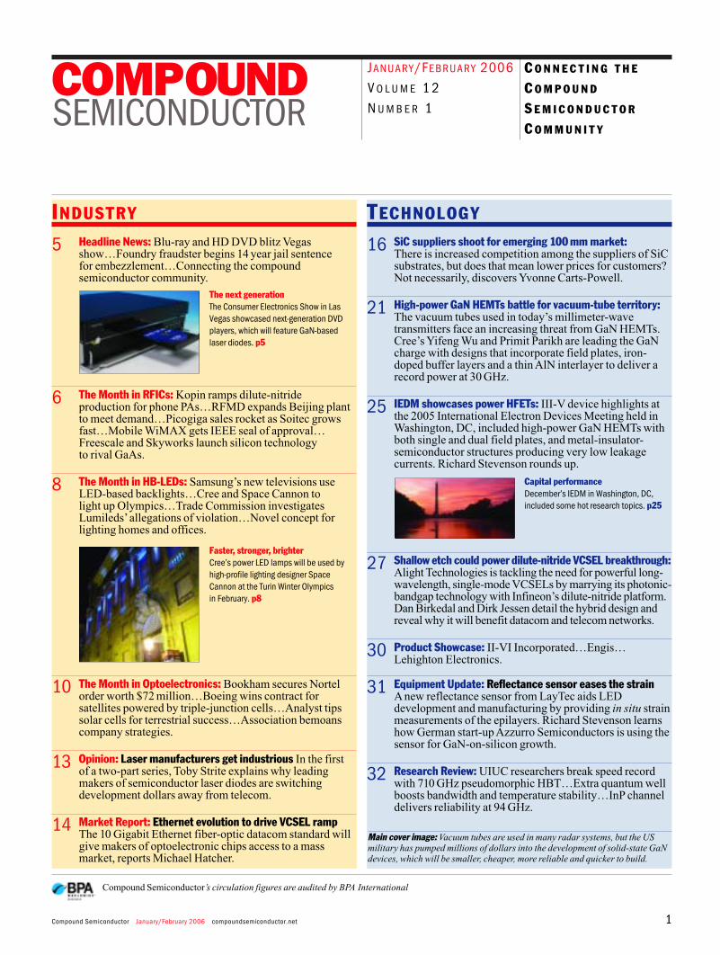
16 SiC suppliers shoot for emerging 100 mm market:There is increased competition among the suppliers of SiC substrates, but does that mean lower prices for customers? Not necessarily, discovers Yvonne Carts-Powell.
21 High-power GaN HEMTs battle for vacuum-tube territory:The vacuum tubes used in today’s millimeter-wave transmitters face an increasing threat from GaN HEMTs.Cree’s Yifeng Wu and Primit Parikh are leading the GaN charge with designs that incorporate field plates, iron-doped buffer layers and a thin AlN interlayer to deliver a record power at 30 GHz.
25 IEDM showcases power HFETs: III-V device highlights at the 2005 International Electron Devices Meeting held in Washington, DC, included high-power GaN HEMTs withboth single and dual field plates, and metal-insulator-semiconductor structures producing very low leakage currents. Richard Stevenson rounds up.
27 Shallow etch could power dilute-nitride VCSEL breakthrough:Alight Technologies is tackling the need for powerful long-wavelength, single-mode VCSELs by marrying its photonic-bandgap technology with Infineon’s dilute-nitride platform. Dan Birkedal and Dirk Jessen detail the hybrid design and reveal why it will benefit datacom and telecom networks.
30 Product Showcase: II-VI Incorporated…Engis…Lehighton Electronics.
31 Equipment Update: Reflectance sensor eases the strainA new reflectance sensor from LayTec aids LED development and manufacturing by providing in situ strain measurements of the epilayers. Richard Stevenson learns how German start-up Azzurro Semiconductors is using the sensor for GaN-on-silicon growth.
32 Research Review: UIUC researchers break speed record with 710 GHz pseudomorphic HBT…Extra quantum well boosts bandwidth and temperature stability…InP channel delivers reliability at 94 GHz.
Capital performanceDecember’s IEDM in Washington, DC,included some hot research topics. p25
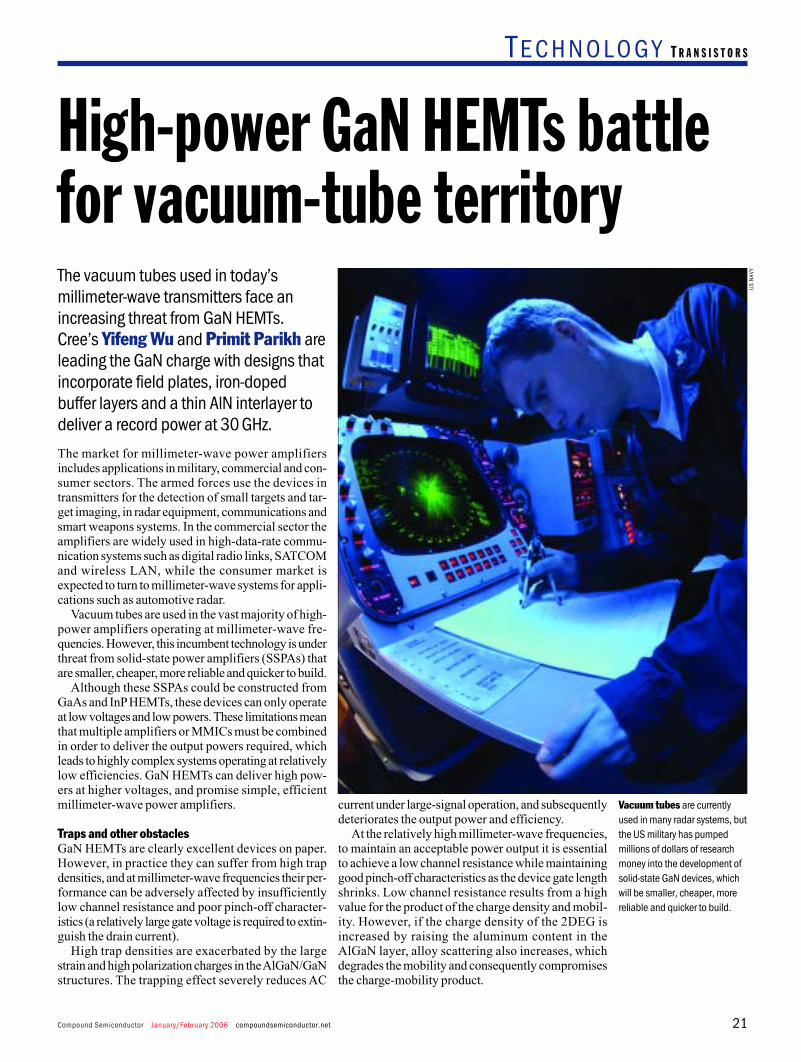
Main cover image: Vacuum tubes are used in many radar systems, but the USmilitary has pumped millions of dollars into the development of solid-state GaNdevices, which will be smaller, cheaper, more reliable and quicker to build.
Compound Semiconductor’s circulation figures are audited by BPA International
INDUSTRY
5 Headline News: Blu-ray and HD DVD blitz Vegas show…Foundry fraudster begins 14 year jail sentence for embezzlement…Connecting the compound semiconductor community.
6 The Month in RFICs: Kopin ramps dilute-nitride production for phone PAs…RFMD expands Beijing plant to meet demand…Picogiga sales rocket as Soitec grows fast…Mobile WiMAX gets IEEE seal of approval… Freescale and Skyworks launch silicon technology to rival GaAs.
8 The Month in HB-LEDs: Samsung’s new televisions use LED-based backlights…Cree and Space Cannon tolight up Olympics…Trade Commission investigates Lumileds’allegations of violation…Novel concept for lighting homes and offices.
10 The Month in Optoelectronics: Bookham secures Nortel order worth $72 million…Boeing wins contract for satellites powered by triple-junction cells…Analyst tips solar cells for terrestrial success…Association bemoans company strategies.
13 Opinion: Laser manufacturers get industrious In the first of a two-part series, Toby Strite explains why leading makers of semiconductor laser diodes are switching development dollars away from telecom.
14 Market Report: Ethernet evolution to drive VCSEL rampThe 10 Gigabit Ethernet fiber-optic datacom standard willgive makers of optoelectronic chips access to a mass market, reports Michael Hatcher.
Faster, stronger, brighterCree’s power LED lamps will be used byhigh-profile lighting designer SpaceCannon at the Turin Winter Olympics in February. p8
The next generationThe Consumer Electronics Show in LasVegas showcased next-generation DVDplayers, which will feature GaN-based laser diodes. p5
compoundsemiconductor.net January/February 2006 Compound Semiconductor2
COMPOUNDSEMICONDUCTOR
E D I T O R I A L
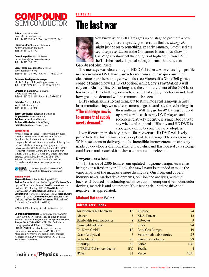
The last warYou know when Bill Gates gets up on stage to promote a newtechnology there’s a pretty good chance that the ubergeekmight just be on to something. In early January, Gates used hiskeynote presentation at the Consumer Electronics Show in Las Vegas to show off the delights of high-definition DVD, the Toshiba-backed optical storage format that relies on
GaN-based blue lasers.The message was clear enough – HD DVD is here. As well as high-profile
next-generation DVD hardware releases from all the major consumerelectronics suppliers, this year will also see Microsoft’s Xbox 360 gamesconsole feature a new HD DVD option, while Sony’s PlayStation 3 willrely on a Blu-ray Disc. So, at long last, the commercial era of the GaN laserhas arrived. The challenge now is to ensure that supply meets demand. Justhow great that demand will be remains to be seen.
Bill’s enthusiasm is no bad thing, but to stimulate a real ramp-up in GaNlaser manufacturing, we need consumers to go out and buy the technology in
their millions. Will they go for it? Having coughedup hard-earned cash to buy DVD players andrecorders relatively recently, it is much too early tosay whether the appeal of Blu-ray and HD DVD isenough to extend beyond the early adopters.
Even if consumers do buy into it, Blu-ray versus HD DVD will likelyprove to be the last format war over optical data storage. The emergence ofWeb-based content delivery and the incredible improvements in capacitymade by developers of much smaller hard-disk and flash-based data storagecould soon make such skirmishes a commercial irrelevance.
New year – new lookThis first issue of 2006 features our updated magazine design. As well asbringing in a fresher overall look, the new layout is intended to make thevarious parts of the magazine more distinctive. Our front-end coversindustry news, market developments, opinion and analysis, with the back-end focused on technological innovation in compound semiconductordevices, materials and equipment. Your feedback – both positive andnegative – is appreciated.
Michael Hatcher Editor
“The challenge now is to ensure that supplymeets demand.”
Air Products & Chemicals 15Aixtron 3Bandwidth Semiconductor 8Crosslight Software 30Epi Nova GmbH 18Evans Analytical 7GaAs Mantech 20IntelliEpi 30INTRINSIC Semiconductor IFCJPSA 11
K Space 24KLA-Tencor 12Raboutet 9Riber 24Semi Con Europa 19Semi-South Laboratories 29Shiva Technologies 29Soitec IBCTecdia 4Veeco OBC
Advertisers’ Index
Editor Michael [email protected]: +44 117 930 1013. Fax: +44 117 925 1942
Features editor Richard [email protected]: +44 117 930 1192
Consulting editor Tim [email protected]: +44 117 930 1233
Senior sales executive David [email protected]: +44 117 930 1032. Fax: +44 117 920 0977
Business development managerMolly Phillips. [email protected]: +1 215 627 0880. Fax: +1 215 627 0879
Circulation manager Jackie [email protected]: +44 117 930 1218. Fax +44 117 930 1178
Publisher Sarah [email protected]: +44 117 930 1020
Senior production editor Ruth LeopoldAd production Mark TrimnellArt director Andrew GiaquintoTechnical illustrator Alison ToveyPublishing director Richard Roe
SubscriptionsAvailable free of charge to qualifying individualsworking at compound semiconductor fabs andfoundries. For further information visitcompoundsemiconductor.net/subscribe. Subscriptionsfor individuals not meeting qualifying criteria:individual £86/$155 US/7125; library £193/$348US/7280. Orders to Compound Semiconductor, WDIS, Units 12 & 13, Cranleigh Gardens IndustrialEstate, Southall, Middlesex UB1 2DB, UK. Tel: +44 208 606 7518; Fax: +44 208 606 7303. General enquiries: [email protected].
8759 total qualified circulation**June 2005 BPA audit statement
Editorial boardMayank Bulsara Atlas Technology (USA); Andrew Carter Bookham Technology (UK); Jacob TarnEpistar/Gigacomm (Taiwan); Ian Ferguson GeorgiaInstitute of Technology (USA); Toby Strite JDSUniphase (USA); Mark Wilson Motorola (USA); Dwight Streit Northrop Grumman (USA); Joseph SmartCrystal IS (USA); Colombo Bolognesi Simon FraserUniversity (Canada); Shuji Nakamura University ofCalifornia at Santa Barbara (USA)
©2006 IOP Publishing Ltd. All rights reserved.
US mailing information: Compound Semiconductor(ISSN 1096-598X) is published 11 times a year for $148 by Institute of Physics Publishing, Dirac House,Temple Back, Bristol BS1 6BE, UK. Periodicalspostage paid at Middlesex, NJ 08846. POSTMASTER: send address corrections toCompound Semiconductor, c/o PO Box 177,Middlesex, NJ 08846. US agent: Pronto MailersAssociation Inc, 200 Wood Avenue, PO Box 177,Middlesex, NJ 08846.
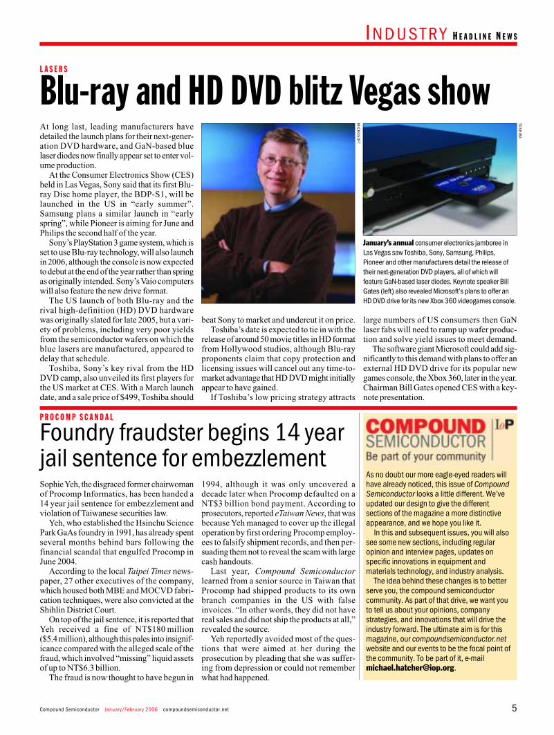
Compound Semiconductor January/February 2006 compoundsemiconductor.net 5
I NDUSTRY H E A D L I N E N E W S
At long last, leading manufacturers havedetailed the launch plans for their next-gener-ation DVD hardware, and GaN-based bluelaser diodes now finally appear set to enter vol-ume production.
At the Consumer Electronics Show (CES)held in Las Vegas, Sony said that its first Blu-ray Disc home player, the BDP-S1, will belaunched in the US in “early summer”.Samsung plans a similar launch in “earlyspring”, while Pioneer is aiming for June andPhilips the second half of the year.
Sony’s PlayStation 3 game system, which isset to use Blu-ray technology, will also launchin 2006, although the console is now expectedto debut at the end of the year rather than springas originally intended. Sony’s Vaio computerswill also feature the new drive format.
The US launch of both Blu-ray and therival high-definition (HD) DVD hardwarewas originally slated for late 2005, but a vari-ety of problems, including very poor yieldsfrom the semiconductor wafers on which theblue lasers are manufactured, appeared todelay that schedule.
Toshiba, Sony’s key rival from the HDDVD camp, also unveiled its first players forthe US market at CES. With a March launchdate, and a sale price of $499, Toshiba should
beat Sony to market and undercut it on price.Toshiba’s date is expected to tie in with the
release of around 50 movie titles in HD formatfrom Hollywood studios, although Blu-rayproponents claim that copy protection andlicensing issues will cancel out any time-to-market advantage that HD DVD might initiallyappear to have gained.
If Toshiba’s low pricing strategy attracts
large numbers of US consumers then GaNlaser fabs will need to ramp up wafer produc-tion and solve yield issues to meet demand.
The software giant Microsoft could add sig-nificantly to this demand with plans to offer anexternal HD DVD drive for its popular newgames console, the Xbox 360, later in the year.Chairman Bill Gates opened CES with a key-note presentation.
Blu-ray and HD DVD blitz Vegas show
January’s annual consumer electronics jamboree inLas Vegas saw Toshiba, Sony, Samsung, Philips,Pioneer and other manufacturers detail the release oftheir next-generation DVD players, all of which willfeature GaN-based laser diodes. Keynote speaker BillGates (left) also revealed Microsoft’s plans to offer anHD DVD drive for its new Xbox 360 videogames console.
Sophie Yeh, the disgraced former chairwomanof Procomp Informatics, has been handed a14 year jail sentence for embezzlement andviolation of Taiwanese securities law.
Yeh, who established the Hsinchu SciencePark GaAs foundry in 1991, has already spentseveral months behind bars following thefinancial scandal that engulfed Procomp inJune 2004.
According to the local Taipei Times news-paper, 27 other executives of the company,which housed both MBE and MOCVD fabri-cation techniques, were also convicted at theShihlin District Court.
On top of the jail sentence, it is reported thatYeh received a fine of NT$180 million($5.4million), although this pales into insignif-icance compared with the alleged scale of thefraud, which involved “missing” liquid assetsof up to NT$6.3 billion.
The fraud is now thought to have begun in
1994, although it was only uncovered adecade later when Procomp defaulted on aNT$3 billion bond payment. According toprosecutors, reported eTaiwan News, that wasbecause Yeh managed to cover up the illegaloperation by first ordering Procomp employ-ees to falsify shipment records, and then per-suading them not to reveal the scam with largecash handouts.
Last year, Compound Semiconductorlearned from a senior source in Taiwan thatProcomp had shipped products to its ownbranch companies in the US with falseinvoices. “In other words, they did not havereal sales and did not ship the products at all,”revealed the source.
Yeh reportedly avoided most of the ques-tions that were aimed at her during theprosecution by pleading that she was suffer-ing from depression or could not rememberwhat had happened.
Foundry fraudster begins 14 yearjail sentence for embezzlement
As no doubt our more eagle-eyed readers willhave already noticed, this issue of CompoundSemiconductor looks a little different. We’veupdated our design to give the differentsections of the magazine a more distinctiveappearance, and we hope you like it.
In this and subsequent issues, you will alsosee some new sections, including regularopinion and interview pages, updates onspecific innovations in equipment andmaterials technology, and industry analysis.
The idea behind these changes is to betterserve you, the compound semiconductorcommunity. As part of that drive, we want youto tell us about your opinions, companystrategies, and innovations that will drive theindustry forward. The ultimate aim is for thismagazine, our compoundsemiconductor.netwebsite and our events to be the focal point ofthe community. To be part of it, [email protected].
P R O C O M P S C A N D A L
L A S E R S
TOS
HIB
A
MIC
RO
SO
FT
compoundsemiconductor.net January/February 2006 Compound Semiconductor6
I NDUSTRY T H E M O N T H I N R F I C S
E P I W A F E R S
Key HBT epiwafer supplier Kopin says that ithas begun volume production of GaAsInN(GAIN) material destined to be used in cell-phone handset power amplifiers (PAs).
The company, which has worked on thedevelopment of the advanced technology withPAsupplier Skyworks Solutions, expects “tensof millions” of faster PAs to be manufacturedusing the GAIN-HBT epiwafers with just theinitial design-ins. It is forecasting weeklywafer shipments in the “low hundreds”throughout 2006, and has already dispatchedcircuits featuring this technology.
“The addition of indium and nitrogenreduces the bandgap energy for low-voltageoperation, and the gradually varying compo-sition creates an internal electric field forhigher-speed operation,” explained RogerWelser, who has led the development of thenew material. The key GAIN base epilayer is50 nm thick, and InGaP and GaAs layers areused for the emitter and collector, respectively.
In addition, says Welser, the greater bandgap
difference between the GAIN-HBT emitterand base layer (compared with conventionalInGaP HBTs) improves PAreliability.
Other advantages over InGaPinclude a baselayer that allows good PAperformance acrossa wider temperature range, and “potentiallyhigher power efficiency”.
Matthew Micci, Kopin’s vice-president ofsales, GaAs products, told Compound Semi-conductor that the various improvements willenable handset makers to produce cheaperphones containing fewer parts that are morerobust and less affected by temperature change.
Thanks to the close collaboration withSkyworks, the GAIN material, which is grownon both 4 inch and 6 inch substrates, can sim-ply be dropped into the processing line in placeof the InGaP wafers previously used.
Kopin revealed the start of volume pro-duction at the IEEE Topical Workshop inPower Amplifiers for Wireless Communi-cation, which took place in San Diego, CA,on January 15–20.
Kopin ramps dilute-nitrideproduction for phone PAs
Picogiga, the French company that specializesin GaN-on-silicon and silicon-on-polycrys-talline-SiC material, is on track to double itsannual sales.
According to its parent company Soitec,which supplies silicon-on-insulator (SOI)wafers, in the nine months of the current fis-cal year Picogiga’s sales have grown by 76.5%.
Already spectacular, that growth shouldincrease over the next quarter, says Soitec, withthe full-year Picogiga revenue for 2005–2006set to double the 2004–2005 figure.
In the most recent quarter Picogiga’s salessurged to 72.6 million ($3.1 million).
Meanwhile, the parent company is enjoy-ing similar success, saying that the “era of theSOI wafer has arrived”. That appears to be thecase: in a red-hot market, Soitec has increasedits financial guidance on three occasions in thelast year. Thanks largely to AMD’s successwith SOI-based processors, total sales at Soitecmore than doubled from last year to reach770.9 million in the most recent quarter,prompting the third guidance notice.
AMD has now signed a whopping $150mil-lion contract with Soitec for calendar 2006.The two companies agreed a long-term deal in2005 under which Soitec is supplying both200 mm and 300 mm wafers manufacturedusing the so-called “Smart Cut” process.
Picogiga has also developed this process forGaN material, while Soitec is working onstrained-silicon epiwafers and germanium-on-insulator technology.
Picogiga sales rocketas Soitec grows fast
RF Micro Devices’ (RFMD’s) board of dir-ectors has approved the expansion of the com-pany’s assembly operations, which are locatedin Beijing, China.
The expansion, which is expected to be upand running during the June quarter of 2006,should increase RFMD’s internal-assemblycapacity by 50%. It will also enable theGreensboro, NC, company to meet a quarterof its assembly requirements in-house.
“Expanding assembly capacity is consis-tent with our overall goal of improving prof-itability,” said company CFO Dean Priddy.
“Our in-house assembly products havelower manufacturing costs, allowing improvedgross margin versus components assembledby third parties,” he continued.
RFMD expands Beijingplant to meet demand
A S S E M B LY
F I N A N C E
From our Web pages...visit compoundsemiconductor.net for daily news updates
…two-stage power amplifierW J Communications has expanded its portfolioof InGaP HBT intermediate power amplifiers withthe release of its AH212 device. The componentis a 1 W, high dynamic range, two-stage driveramplifier optimized for a range of next-generation wireless technologies includingGPRS, GSM, CDMA and W-CDMA.
…MBE reactor salesEpitaxy equipment supplier Veeco Instrumentshas received orders for GEN2000 MBE systemsfrom two leading suppliers of RFICs used inmobile applications. The customers will use the7 × 6 inch multi-wafer systems for themanufacture of GaAs-based ICs used in poweramplifiers (PAs) and deployed in handsets andwireless LANs (WLANs).
…wireless modulesAnadigics has unveiled two integrated circuitsfor wireless LAN (WLAN) and multiple inputmultiple output (MIMO) applications thatcombine the power amplifier, low-noise
amplifier, and RF antenna switch on a singledie. “Unlike other RF front-end solutions,Anadigics’ AWL6254 and AWL6255 are offeredin an ultra-low-profile plastic package meetingthe latest height requirements for use inconsumer electronics, such as mobile phones,cameras, PDAs, and game controllers,” saidRon Michels, general manager of broadbandproducts at Anadigics.
…executive changesFabless manufacturer of RF devices HittiteMicrowave has promoted Brian Jablonski fromdirector of operations to vice-president ofoperations. In his new role he will oversee thecompany’s supply-chain management andmanufacturing operations.
…GaN HEMTsHitachi Cable has qualified Aixtron’s Close-Coupled Showerhead (CCS) system for thegrowth of GaN HEMT structures suitable forbase-station and mobile telecommunicationapplications.
INDUSTRY T H E M O N T H I N R F I C S
Compound Semiconductor January/February 2006 compoundsemiconductor.net 7
R E G U L A T I O N S C O M P O N E N T S
RF chipmakers Freescale and Skyworks arelaunching silicon-based amplifiers andswitches to complement their GaAs products.
Freescale has developed a power amplifierfor 3.5GHz WiMAX applications that is basedon silicon LDMOS technology. The com-pany’s power transistor, which it says is thefirst LDMOS device to meet the stringentrequirements for WiMAX base stations, couldprove to be a tough competitor to GaAs- andGaN-based alternatives in the 3.5 GHz band.
The DMOS transistor is available for sam-pling and can deliver an output of 16 W, whiletwo similar devices will be released soon.
However, Freescale is also continuing todevelop its high-voltage GaAs PHEMTs oper-ating up to 6 GHz for use in more demandingWiMAX systems and other applications.
Meanwhile, Skyworks is ramping produc-tion of two of its CMOS switches for satellitereceiver applications. The Woburn-based com-
pany says that its switches (SKY13264- 360LFand SKY13264-340LF) are cheaper, easier toimplement, and provide greater integrationthan those using either GaAs or discrete sili-con technologies.
The switches can be used in equipment thatcan receive signals from multiple satellitesand access hundreds of different channels withjust one dish. “We are capturing substantialmarket share just six months after the intro-duction of our RF CMOS solution,” said StanSwearingen, Skyworks’ general manager oflinear products.• Another silicon-based RF switch technology,silicon-on-sapphire, is being offered byPeregrine Semiconductor. The company saysthat its PE42671 switch, which rivals GaAsPHEMTs and is suitable for WCDMA andGSM networks, can reduce the overall partcount in an antennae switch module by as manyas six devices and thirteen wire bonds.
Evans Analytical Group
SM
EAG SIMS Technology
Advances at EAGMost Accurate SIMS Characterization of
• Shallow Boron, Arsenic, Phosphorus Implants
• SiGe and devices
• Ultra thin (1nm) SiON
• Very small area (10 x 10µm) devices
• Dopants and Impurities of SOI films
• SiC and GaN
Al
C
SiO
Cl
F
N
0 2 4 6 8
Depth (microns)
1E+14
1E+15
1E+16
1E+17
1E+18
1E+19
1E+20
1E+21
Co
nce
ntr
atio
n (
at/
cm
3)
1E+00
1E+01
1E+02
1E+03
1E+04
1E+05
Co
un
ts P
er
Se
co
nd
Small (50µm dia.) Area Analysis on a VCSEL Device
1E+06
10 12
Characterization of Multi-Compositional III-V epitaxial Films
• AlGaAs, InGaP, GaInAsN, InGaAsSb, InP: HBT, FET
• AlGaAs/InGaAs, AlGaAs/InGaP: HEMT
• AlGaAs/InGaAlP/InGaP: VCSEL• AlGaAs/InGaAs: Laser• InGaAlP, GaN/InGaN: LED, HEMT
cascadescientific
R
We are nowONE Company!
Contact us at : [email protected]
www.eaglabs.com
SEMICON Korea Booth 813
SEMICON China Booth 3750
Evans Analyt ical Group
810 Ki fer Road
Sunnyvale, CA 94086
+1 408 530 3500
Ad_C.ai 1/11/2006 9:57:32 AM
Freescale and Skyworks launchsilicon technology to rival GaAsIn a move that should help the development of
broadband wireless access (BWA) systemsacross the globe, the IEEE has approved the802.16e “WiMAX” standard.
RF chipmakers will welcome the move,which extends the existing 802.16 standardthat addressed wireless metropolitan-areanetworks (WMANs) for broadband accessbut previously supported only fixed, or sta-tionary, terminals. The new standard coversfixed and mobile BWA subscriber stationsmoving at speeds typical of car travel. MobileWiMAX will operate in licensed bandsbelow 6 GHz.
Anumber of compound semiconductor chipcompanies, such as Nitronex, Cree, EudynaDevices and TriQuint Semiconductor, are tar-geting WiMAX already, with componentsbased on GaAs, SiC or GaN transistors.
Semiconductor suppliers have been heav-ily involved in the development of the stan-dard in the past three years, said Roger Marks,the chair of the IEEE 802.16 working groupon BWA. “The foundation for a global indus-try is now in place,” he added.
Acknowledging that the road to develop-ment had been both long and difficult, BrianKiernan, who led the IEEE mobile WiMAXtask group, said: “The [new] standard givesservice operators the ability to provide a widerange of revolutionary high-speed, mobilewireless applications and services that willgreatly improve people’s way of life.”
The precise application areas where mobileWiMAX will end up deployed are not yetfixed, since the protocol faces stiff competi-tion from other broadband services such asthird-generation cellular technology.
One theory is that mobile WiMAX couldprosper in more remote locations where cel-lular coverage is patchy or non-existent.However, to win this business it will have tobattle against the satellite-phone technologythat is also targeting this particular market.
Unsurprisingly, WiMAX Forum presidentRon Resnick welcomed the approval of thestandard. “The WiMAX Forum and its mem-bers can now move forward with confidenceas we collaborate to ensure that certified prod-ucts arrive by late this year or early 2007,”Resnick said. “We have already achievedaccelerated progress by developing systemprofiles based on the 802.16e specification andidentifying conformance test tools and meth-ods,” he added.
Compound semiconductor firms in theWiMAX Forum include TriQuint, M/A-COM,Skyworks Solutions and Filtronic.
Mobile WiMAX getsIEEE seal of approval
compoundsemiconductor.net January/February 2006 Compound Semiconductor8
I NDUSTRY T H E M O N T H I N H B - L E D S
A P P L I C A T I O N S
The Korean consumer electronics giantSamsung has unveiled some high-end televi-sions that feature LED-based backlights.
LED manufacturers are pinning their hopeson backlighting of large-area displays as a keynew market for their devices as growth is slow-ing in today’s biggest application area – illu-mination of cell-phone keypads and screens.
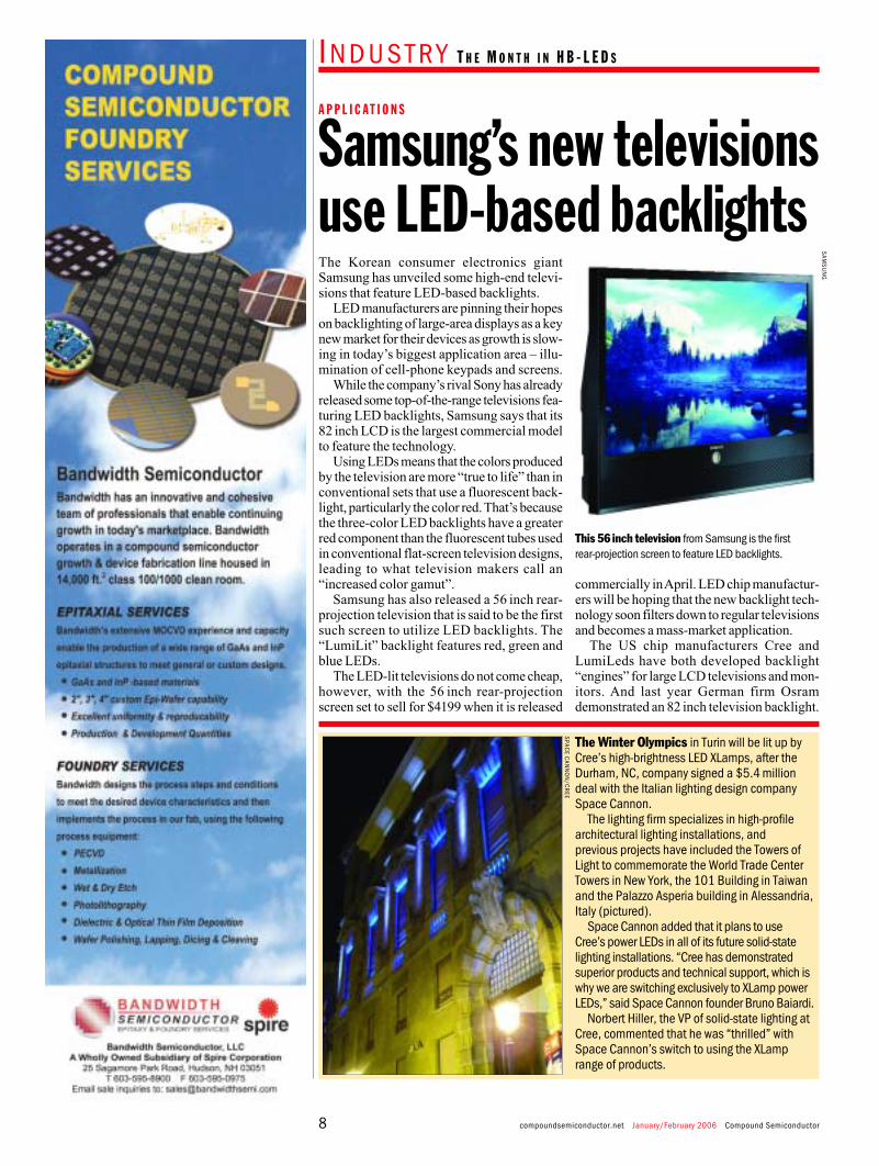
While the company’s rival Sony has alreadyreleased some top-of-the-range televisions fea-turing LED backlights, Samsung says that its82 inch LCD is the largest commercial modelto feature the technology.
Using LEDs means that the colors producedby the television are more “true to life” than inconventional sets that use a fluorescent back-light, particularly the color red. That’s becausethe three-color LED backlights have a greaterred component than the fluorescent tubes usedin conventional flat-screen television designs,leading to what television makers call an“increased color gamut”.
Samsung has also released a 56 inch rear-projection television that is said to be the firstsuch screen to utilize LED backlights. The“LumiLit” backlight features red, green andblue LEDs.
The LED-lit televisions do not come cheap,however, with the 56 inch rear-projectionscreen set to sell for $4199 when it is released
commercially in April. LED chip manufactur-ers will be hoping that the new backlight tech-nology soon filters down to regular televisionsand becomes a mass-market application.
The US chip manufacturers Cree andLumiLeds have both developed backlight“engines” for large LCD televisions and mon-itors. And last year German firm Osramdemonstrated an 82 inch television backlight.
Samsung’s new televisionsuse LED-based backlights
This 56 inch television from Samsung is the first rear-projection screen to feature LED backlights.
SAM
SU
NG
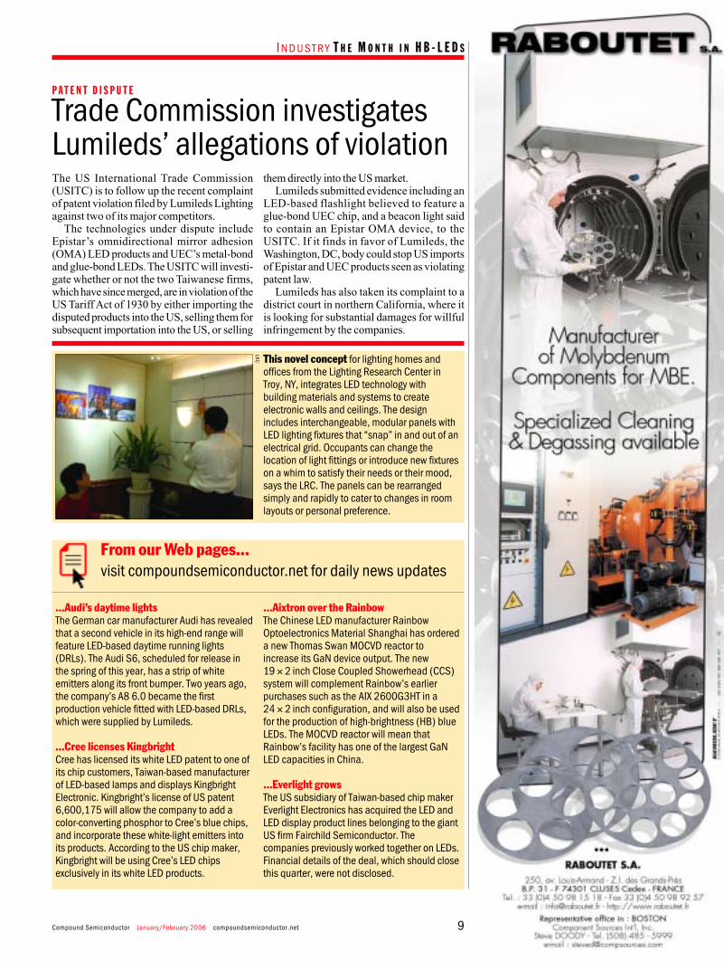
The Winter Olympics in Turin will be lit up byCree’s high-brightness LED XLamps, after theDurham, NC, company signed a $5.4 milliondeal with the Italian lighting design companySpace Cannon.
The lighting firm specializes in high-profilearchitectural lighting installations, and previous projects have included the Towers ofLight to commemorate the World Trade CenterTowers in New York, the 101 Building in Taiwanand the Palazzo Asperia building in Alessandria,Italy (pictured).
Space Cannon added that it plans to useCree’s power LEDs in all of its future solid-statelighting installations. “Cree has demonstratedsuperior products and technical support, which iswhy we are switching exclusively to XLamp powerLEDs,” said Space Cannon founder Bruno Baiardi.
Norbert Hiller, the VP of solid-state lighting atCree, commented that he was “thrilled” withSpace Cannon’s switch to using the XLamprange of products.
SPAC
E CAN
NO
N/C
REE
INDUSTRY T H E M O N T H I N H B - L E D S
Compound Semiconductor January/February 2006 compoundsemiconductor.net 9
P A T E N T D I S P U T E
The US International Trade Commission(USITC) is to follow up the recent complaintof patent violation filed by Lumileds Lightingagainst two of its major competitors.
The technologies under dispute includeEpistar’s omnidirectional mirror adhesion(OMA) LED products and UEC’s metal-bondand glue-bond LEDs. The USITC will investi-gate whether or not the two Taiwanese firms,which have since merged, are in violation of theUS Tariff Act of 1930 by either importing thedisputed products into the US, selling them forsubsequent importation into the US, or selling
them directly into the US market.Lumileds submitted evidence including an
LED-based flashlight believed to feature aglue-bond UEC chip, and a beacon light saidto contain an Epistar OMA device, to theUSITC. If it finds in favor of Lumileds, theWashington, DC, body could stop US importsof Epistar and UEC products seen as violatingpatent law.
Lumileds has also taken its complaint to adistrict court in northern California, where itis looking for substantial damages for willfulinfringement by the companies.
Trade Commission investigatesLumileds’ allegations of violation
This novel concept for lighting homes andoffices from the Lighting Research Center inTroy, NY, integrates LED technology withbuilding materials and systems to createelectronic walls and ceilings. The designincludes interchangeable, modular panels withLED lighting fixtures that “snap” in and out of anelectrical grid. Occupants can change thelocation of light fittings or introduce new fixtureson a whim to satisfy their needs or their mood,says the LRC. The panels can be rearrangedsimply and rapidly to cater to changes in roomlayouts or personal preference.
LRC
From our Web pages...visit compoundsemiconductor.net for daily news updates
...Audi’s daytime lightsThe German car manufacturer Audi has revealedthat a second vehicle in its high-end range willfeature LED-based daytime running lights(DRLs). The Audi S6, scheduled for release inthe spring of this year, has a strip of whiteemitters along its front bumper. Two years ago,the company’s A8 6.0 became the firstproduction vehicle fitted with LED-based DRLs,which were supplied by Lumileds.
...Cree licenses KingbrightCree has licensed its white LED patent to one ofits chip customers, Taiwan-based manufacturerof LED-based lamps and displays KingbrightElectronic. Kingbright’s license of US patent6,600,175 will allow the company to add acolor-converting phosphor to Cree’s blue chips,and incorporate these white-light emitters intoits products. According to the US chip maker,Kingbright will be using Cree’s LED chipsexclusively in its white LED products.
...Aixtron over the RainbowThe Chinese LED manufacturer RainbowOptoelectronics Material Shanghai has ordereda new Thomas Swan MOCVD reactor toincrease its GaN device output. The new19 × 2 inch Close Coupled Showerhead (CCS)system will complement Rainbow’s earlierpurchases such as the AIX 2600G3HT in a24 × 2 inch configuration, and will also be usedfor the production of high-brightness (HB) blueLEDs. The MOCVD reactor will mean thatRainbow’s facility has one of the largest GaNLED capacities in China.
...Everlight growsThe US subsidiary of Taiwan-based chip makerEverlight Electronics has acquired the LED andLED display product lines belonging to the giantUS firm Fairchild Semiconductor. Thecompanies previously worked together on LEDs.Financial details of the deal, which should closethis quarter, were not disclosed.

compoundsemiconductor.net January/February 2006 Compound Semiconductor10
I NDUSTRY T H E M O N T H I N O P T O E L E C T R O N I C S
F I N A N C E
Optical component and module vendorBookham has secured a supply agreement withNortel Networks that will guarantee it at least$72 million in sales this year.
The Canadian network equipment supplierhas long been Bookham’s key customer, par-ticularly since the acquisition of Nortel’s opti-cal components business back in 2002.
The latest deal replaces the agreement thatBookham and Nortel reached last year, andwhich was scheduled to expire in late April.In recent quarters, Nortel has been responsi-ble for around half of Bookham’s overall sales.
Bookham, which manufactures InP-basedoptoelectronic chips at its facility in Caswell,UK, has also paid off around $65 million of itslong-term debt, including a Nortel loan.
The total included a cash payment of$20 million plus interest to Nortel, as well asthe issue of more than 10 million new sharesand warrants to buy more stock to institutionalinvestors who will take on some of Bookham’sdebt. The share warrants have an exercise priceof $7 and can be used over the next five years.
In a third transaction, $19.4 million of out-standing debentures were converted in a stock-and-cash deal. Bookham now plans toeliminate its remaining $6.1 million of deben-ture-related debt in a similar move that willrequire shareholder approval.
While Bookham’s share price dipped byalmost 10% on news of the refinancing, theamount of extra stock issued meant that thecompany’s market valuation increased.
Bookham secures Nortelorder worth $72 million
...Avanex shortfallAvanex saw a substantial shortfall in revenue forits latest financial quarter because of a contractmanufacturing problem that delayed productshipments. As Compound Semiconductor wentto press, Avanex estimated sales of$35 million–$37 million for the three monthsending on December 31, 2005, much less thanthe $41 million–$45 million originally forecast.Paul Negus, the company’s vice-president ofoperations, resigned in early January.
...European researchEurope has a new body championing thecause of photonics research thanks to thecreation of “Photonics 21”. More than 200experts from 16 European member states and120 companies celebrated the launch event inBrussels, Belgium, last December.
The group was set up by the EuropeanPhotonics Industry Consortium (EPIC). Itsmembers include key MOCVD equipmentsupplier Aixtron, sapphire substrate makerCrystalQ, GaN specialist Picogiga and epiwaferfoundry IQE. Also involved are a host of chipmanufacturers including Bookham, OsramOpto Semiconductors and Jenoptik, as well asend-users of optoelectronic technology suchas Audi and Philips Lighting.
...Army likes InGaAsGoodrich Corporation’s optical and spacesystems team, formerly known as SensorsUnlimited, has won a $750 000 developmentcontract from the US Army to improve InGaAsdevice manufacturing. The army wants thePrinceton, NJ, firm to deliver a detector arrayfor night vision that can record high-definitionimages in the infrared range whilesimultaneously capturing visible-rangeimagery. The proposed 1920 × 1080 pixelcameras should also show an improvement insensitivity, and detect light in an unspecified“new” wavelength band.
Martin Ettenberg’s Goodrich team will focuson improving the design of the chips usedwithin the camera. “These improvements willresult in higher device yields, which will lowerthe cost per unit and provide much highersensitivity in dark or low-light conditions,”added the company.
...Firecomms expansionFirecomms, the Ireland-based developer ofhigh-speed semiconductor light sources, hasopened regional offices to provide sales andapplication support in Houston, US, andYokohama, Japan.
Boeing is to build three huge communicationssatellites, all of which will be powered bytriple-junction GaAs solar cells. Expected tolaunch around 2009, the satellites have beenordered by the US communications companyMobile Satellite Ventures (MSV).
Boeing is likely to award the lucrative con-tract for the solar cells for the satellites to itsCalifornian chip-making subsidiary Spectrolab,its rival Emcore, or both companies.
Construction of the first satellite will takean estimated 44 months, with the second andthird payloads following a few months later.Boeing said that the MSV deal represented itsbiggest single contract for a satellite systemsince 1997.
After launch, the three satellites will formthe backbone of an advanced network cover-ing North and South America that will delivervoice and data communications using a com-bination of satellite and cellular technologies.
According to MSV, the satellites will workin tandem with ground stations to provide high-speed links in remote areas, and extra capac-ity in cities where satellite signals arefrequently blocked by buildings.
The result should guarantee regular cell-phone users the benefits of a satellite-phoneservice. In the past, similar networks such as
Iridium have demanded much larger phonesto detect the relatively weak satellite signal.
MSV adds that the service should also ben-efit emergency-response teams by ensuringthat cell-phone networks stay connected viathe satellites even if ground stations aredestroyed, as happened when HurricaneKatrina struck the Gulf Coast last year.
The network will have a high powerdemand, so Boeing will use the triple-junctioncells to supply 11kWthrough five-panel arrayson each satellite.
P H O T O V O LT A I C S
Boeing wins contract for satellitespowered by triple-junction cells
From our Web pages...visit compoundsemiconductor.netfor daily news update
Boeing subsidiary Spectrolab and rival Emcore willbe vying for a contract to deliver the GaAs-based solarcells needed for Boeing’s three-satellite deal with MSV.
BO
EING
INDUSTRY T H E M O N T H I N O P T O E L E C T R O N I C S
Compound Semiconductor January/February 2006 compoundsemiconductor.net 11
E M C O R E
Chip manufacturer Emcore will start to see rev-enue from sales of solar cells into terrestrialpower applications this year, according to JohnLau, an analyst with Jeffries and Company.
Compound semiconductor-based solar cellsare much more efficient than silicon-basedcells, but are generally regarded as being muchmore expensive. However, Lau says thatEmcore believes it can now compete on costwith silicon because GaAs-based solar cellscan be designed into “concentrator” systems,where a lens is used to focus sunlight onto amuch smaller area of semiconductor than inconventional systems.
These systems also track the movement ofthe Sun throughout the day, producing a higheroverall electrical power output. While Lau feelsthese designs do not suit residential use, he doesexpect to see them deployed commercially.
Lau adds that Emcore will be aided by thecurrent shortage of polysilicon. There is noshortage of GaAs resources, or the germaniumsubstrates on which the triple-junction cells aremade. He believes that systems using Emcore’s
cells will operate at a cost of $3/Woutput, sim-ilar to the figure for silicon cells. As a result, heexpects the Somerset, NJ, company to see a pos-itive impact on revenue generation in the sec-ond half of 2006.
Emcore also has a potentially lucrative con-tract to supply solar cells to an unspecified satel-lite manufacturer that could generate up to$20.6 million in revenue.
• Emcore’s Ortel division has acquired thefabless laser developer K2 Optronics. Emcorewas already an investor in the Sunnyvale, CA,company, and bought the remaining portion ina stock deal valued at $4.8 million.
K2 specializes in directly modulated exter-nal-cavity lasers (ECLs), which Emcorebelieves could revolutionize cable television(CATV) and fiber-to-the-premises (FTTP)applications. “We expect to see our CATVandFTTPcustomers insist on the performance andcost advantages that directly modulated lasers[based on K2’s ECLtechnology] can offer overtraditional laser technology,” said Hong Hou,
who leads Emcore’s Ortel division. Followinga six-month transition period, K2’s design andengineering teams will be integrated withEmcore’s Santa Clara, CA, design center.
K2 attracted around $45 million in venturefunding before Emcore’s initial investment inthe company in February 2005. Fellow chipmaker JDSU had also invested in prior fund-ing rounds, while K2 boasted that it was the firstcompany to mass-produce packaged ECLsthrough its Thailand-based contract manufac-turing partner Fabrinet.
Emcore expects combined sales of K2’sexisting products and its own directly modu-lated transmitters featuring K2’s lasers to gen-erate about $7 million this year. The Somerset,NJ, company is then anticipating strong growth,leading to sales of $14 million in 2007.
The K2 acquisition is Emcore’s latest movein a bid to increase its presence across the com-munications industry. In the past year it hasacquired JDSU’s cable TV component busi-ness, the optical module supplier Phasebridgeand the video broadcast company Force.
Our advanced 266nmChromaDice™ DPSS laser
system produces 10 wafer/hour LED throughput
with > 99% die yield at < $2 US per wafer.
Visit www.jpsalaser.com today and find out more!
Introducing the compactIX–200MicromachiningSystem
Advanced 266 or 355nm DPSS Laser Process
Narrow Cuts: As Small As 2.5 Microns
Excellent Die Yield: > 99%
Low Operating Cost: < $2 per Wafer
24/7 Maintenance-Free Operation
User-Friendly Windows® 2000™ Software
Automatic Alignment: < 1 Minute to Load & Align
Excellent Results on GaAs, Si and Other Materials
Featuring the JPSA IX–300 System!Speed, Quality, and Reliability
Korea QMC, Ltd., Tel. 82-31-427-0710 Fax 82-31-427-0714Taiwan LST Technology Co., Ltd., Tel. 886-3-6563716 Fax 886-3-6563717Japan Hakuto Co., Ltd., Tel. 81-3-3225-8910 Fax 81-3-3225-9001
J P Sercel Associates, Inc. 17D Clinton Drive, Hollis, New Hampshire 03049 USATel. +1 (603) 595-7048 Fax +1 (603) 598-3835
Asia Representatives:
Analyst tips solar cells for terrestrial success
The US-based Optoelectronics IndustryDevelopment Association (OIDA) says thatthe sector faces a difficult future because of alack of investment in research.
“Unfortunately, the level of research anddevelopment across the industry seems to be lower than that needed to support thecommunications roadmaps [we have] devel-oped,” said OIDAexecutive director MichaelLebby. Last year, Lebby called for the imple-mentation of an optical foundry industrymodel, echoing the findings of a similar study carried out by the MassachusettsInstitute of Technology.
Lebby added that without this investment,the optoelectronics market would be unable tothrive over the next decade.
According to the OIDA, one major problemis the current mindset of chip manufacturerssuch as Bookham and Mitsubishi, whichbelieve that success lies in vertical integrationand high-value, non-standard devices – ratherthan the development of standard platformsthat would lower product costs.
“Because there is no commonality, there are limited economies in manufacturing, and this has led to high cost structures,”bemoaned Lebby.
Association bemoanscompany strategies
R & D
Differentiating between subtle optical characteristics can provide critical information on defects. A particle
under the epi layer is a very different problem than a particle on the surface. Our Optical Surface Analyzers
(OSA) are unique surface inspection systems that employ a combination of measurement technologies
to automatically detect and classify a variety of defects. Defects are binned by size into user-defined
categories, and displayed on a defect map. The OSA images remain linked to the report, for quick and
effective review.
Automatically classifies particles and scratches as “on” versus “in or under” the epi layer
User-defined defect classifications allow automated detection and reporting of unusual defect types
Crystal defects such as dislocations and polytype changes are automatically detected and counted
Manual or automated cassette-to-cassette operation
Accommodates wafer sizes from 50 to 300 mm
For more product information, go to:
Accelerating Yield®
Particle in-epi: bright scatter dark reflected smaller scatter signature
(film thicker over particle)
Particle on-epi: bright scatter dark reflected same optical size
Do you know the three W’s of epi-layerinspection? Only Candela™ finds where it is, what it is, and when it occurred.
©20
05 K
LA-T
enco
r Cor
pora
tion.
www.kla-tencor.com/candela
Compound Semiconductor January/February 2006 compoundsemiconductor.net 13
I NDUSTRY O P I N I O N
During the go-go 1990s, telecom ambitions dominatedthe thoughts of the world’s most capable laser-diodemanufacturers. The handful of firms able to manufac-ture reliable 980nm diode lasers supplied up to $500mil-lion per year of pump-laser modules to the erbium-dopedfiber amplifier (EDFA) market. Even leading lights ofthe industrial lasers arena like Coherent and Spectra-Physics scrambled to upgrade their capabilities to jointhe telecom gold rush because their traditional marketswere puny in comparison.
The telecom boom resulted from huge, unsustainableover-investment. Perhaps less remembered is thedisruptive effect of the EDFA, which attracted all thatcapital. The EDFA represents the difference between asingle wavelength traveling 80 km over fiber betweenexpensive optical–electrical–optical regenerators, and160 wavelengths traveling 600 km at a radically lowertransmission cost per bit.
As optical networks expanded from 4 to 16 to 160wavelengths, the amount of optical pump power neededto fuel an EDFA grew proportionately. In a decade ofwhirlwind productivity, telecom-grade, single spatial-mode 980 nm diode laser power increased at a rate of25% every year. Production efficiencies simultaneouslyenabled falling selling prices. A90 mW, 980 nm pumpmodule that sold for $7000 in 1994 now fetches lessthan $400, representing a 22% annualized price ero-sion. A 500 mW pump now sells below $1000, rep-resenting a more than 26% year-on-year decline indollars per mW over that same period.
Such gaudy figures represent high tech as it shouldbe. In an environment of rapid productivity improve-ment, the entire value chain shares the wealth and thrives.However, despite a newly buoyant telecom market,pump lasers are at an inflection point. Now that a single500 mWpump laser services an entire EDFAgain stage,the previously unquenchable thirst for 980 nm power ina single fiber is largely sated. To continue to feed theEDFA value chain, pump-laser suppliers must eitherinnovate along in a new, as yet undefined, technologi-cal direction, or face commoditization.
This conundrum resembles that recently faced byIntel. For years its technical roadmap focused on speed-ing the microprocessor clock rate – eventually saturat-ing the PC market. But if your Dell has a 2GHz processordoes that leave you pining for 4 GHz? For Intel, the needfor speed has diminished and been replaced by moreuseful things – wireless capability, reduced powerconsumption for extended laptop battery life, and amicroprocessor core with more functionality. We’vebarely heard a peep from marketeers about micro-processor GHz since.
For telecom pump lasers, a value-added lateral inno-vation like Intel’s has not yet been identified. If a singlediode could service multiple gain stages, demand wouldbe rekindled for yet higher power devices deliveringlower overall dollars per mW. However, EDFAs increas-
ingly provide mid-stage wavelength add/drop agility,which decouples the amplification power needed in eachstage. Independent and dynamic control of the amountof pump power reaching separate EDFAstages is lack-ing, and there is no foreseeable solution. Many have con-cluded the fundamental value metric of telecom pumpsis destined to move from dollars per mWtowards strictlydollars per laser, which smacks of commoditization. Asa result, diode-laser research dollars are increasinglybeing redirected towards industrial markets that sustainlong-term growth rates in excess of telecom’s 6–8%.
Let’s quickly recap the telecom-driven diode-laserera. Sleepy research teams that once nestled within large,corporate R&D labs landed at aggressive, medium-sizedcompanies who providedthem with unprecedentedinvestment. The result wastelecommunication-grade980 nm pumps sustainingfacet powers exceeding50 MW/ cm2, representingperhaps the highest man-made energy density shortof a nuclear explosion. Thecompanies transferred theirdiode-laser assembly to Pacific Rim factories as a mat-ter of survival, but are yet to earn sustainable returns.
Today, the few players capable of state-of-the-art vol-ume diode-laser manufacture are lean, scalable and eagerto unleash their highly refined technology into newgrowth markets. The market of choice is solid-state laserpumping for industrial applications. For a second con-secutive decade, disruptive diode-laser advances willyield explosive consequences.
• In our next issue, Toby Strite describes howsemiconductor laser-diode manufacturers willtransform the industrial laser market.
Laser manufacturers get industriousIn the first of a two-part series, TobyStrite explains whyleading makers ofsemiconductor laserdiodes are switchingdevelopment dollarsaway from telecom.
O P T O E L E C T R O N I C S
Toby Strite is marketingmanager for JDSU’s High-PowerLasers group in San Jose, CA. E-mail [email protected].
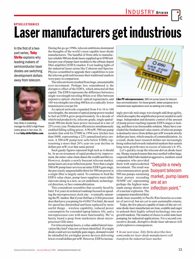
Like PC microprocessors, 980 nm pump lasers for telecom face commoditization. For future growth, better prospects lie inindustrial laser applications such as welding and cutting.
JDS
U
“Despite a newlybuoyant telecommarket, pump lasersare at an inflection point.”
compoundsemiconductor.net January/February 2006 Compound Semiconductor14
I NDUSTRY M A R K E T R E P O R T
With capital expenditure by service providers growing,manufacturers of fiber-optic equipment, modules andcomponents now have less reason to whine than in recentyears. And according to the market analyst companyCommunications Industry Researchers (CIR), the grow-ing popularity of the latest Ethernet data communica-tions standard should soon add some vigor to thatrecovery process.
Having observed the relatively dormant 10 Gbit/sEthernet (10G) market over the past five years, CIR nowbelieves that this protocol is showing signs of becom-ing the general-purpose successor to the widely deployedGigabit Ethernet (1 Gbit/s operation) standard.
Unlike the copper-based Gigabit Ethernet generation,10G is inherently a fiber-optic standard, so it could offeroptical equipment manufacturers, module suppliers andcomponent vendors access to the mass market that theindustry has long craved.
Opportunities for 10G“10G interfaces, which just a few years ago would haveappeared only in a telecom environment, or occasion-ally on the largest Ethernet switches, are now becom-ing common on servers and on modular Ethernetswitches,” says CIR. Although 10G is far from ubiqui-tous – and unlikely to feature on a standard PC for sev-eral years – CIR says that there is now a genuineopportunity for makers of 10G components, who canexpect to sell large volumes of semiconductor chips that
emit and detect rapidly modulating laser light.The type of compound semiconductor components
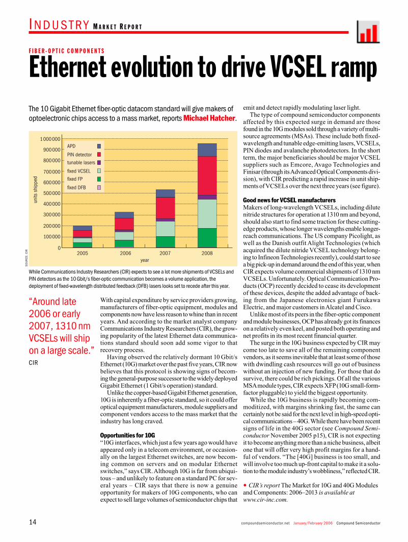
affected by this expected surge in demand are thosefound in the 10G modules sold through a variety of multi-source agreements (MSAs). These include both fixed-wavelength and tunable edge-emitting lasers, VCSELs,PIN diodes and avalanche photodetectors. In the shortterm, the major beneficiaries should be major VCSELsuppliers such as Emcore, Avago Technologies andFinisar (through its Advanced Optical Components divi-sion), with CIR predicting a rapid increase in unit ship-ments of VCSELs over the next three years (see figure).
Good news for VCSEL manufacturersMakers of long-wavelength VCSELs, including dilutenitride structures for operation at 1310 nm and beyond,should also start to find some traction for these cutting-edge products, whose longer wavelengths enable longer-reach communications. The US company Picolight, aswell as the Danish outfit Alight Technologies (whichacquired the dilute nitride VCSEL technology belong-ing to Infineon Technologies recently), could start to seea big pick-up in demand around the end of this year, whenCIR expects volume commercial shipments of 1310 nmVCSELs. Unfortunately. Optical Communication Pro-ducts (OCP) recently decided to cease its developmentof these devices, despite the added advantage of back-ing from the Japanese electronics giant FurukawaElectric, and major customers in Alcatel and Cisco.
Unlike most of its peers in the fiber-optic componentand module businesses, OCPhas already got its financeson a relatively even keel, and posted both operating andnet profits in its most recent financial quarter.
The surge in the 10G business expected by CIR maycome too late to save all of the remaining componentvendors, as it seems inevitable that at least some of thosewith dwindling cash resources will go out of businesswithout an injection of new funding. For those that dosurvive, there could be rich pickings. Of all the variousMSAmodule types, CIR expects XFP(10G small-form-factor pluggable) to yield the biggest opportunity.
While the 10G business is rapidly becoming com-moditized, with margins shrinking fast, the same cancertainly not be said for the next level in high-speed opti-cal communications – 40G. While there have been recentsigns of life in the 40G sector (see Compound Semi-conductor November 2005 p15), CIR is not expectingit to become anything more than a niche business, albeitone that will offer very high profit margins for a hand-ful of vendors. “The [40G] business is too small, andwill involve too much up-front capital to make it a solu-tion to the module industry’s wobbliness,” reflected CIR.
• CIR’s report The Market for 10G and 40G Modulesand Components: 2006–2013 is available at www.cir-inc.com.
Ethernet evolution to drive VCSEL rampThe 10 Gigabit Ethernet fiber-optic datacom standard will give makers ofoptoelectronic chips access to a mass market, reports Michael Hatcher.
F I B E R - O P T I C C O M P O N E N T S
1000000
900000
800000
700000
600000
500000
400000
300000
200000
100000
0
units
shi
pped
year2005 2006 2007 2008
APD
PIN detector
tunable lasers
fixed VCSEL
fixed FP
fixed DFB
While Communications Industry Researchers (CIR) expects to see a lot more shipments of VCSELs andPIN detectors as the 10 Gbit/s fiber-optic communication becomes a volume application, thedeployment of fixed-wavelength distributed feedback (DFB) lasers looks set to recede after this year.
“Around late2006 or early2007, 1310 nmVCSELs will shipon a large scale.”CIR
SO
UR
CE:
CIR

Optoelectronic devices like traffic signals
need to work without fail. Which is why
you need to work with Air Products.
We have the products and experts
to help you optimize your III-V process.
Our SolkatronicTM ultrapure gases include
arsine, high purity ammonia, phosphine and
hydrogen selenide. Our systems maintain
strict control of purity and consistency.
So your films and the devices they control can
set standards for reliability. Whether you’re
in LEDs, lasers, solar cells or other emerging
technologies, visit our web site or call
610-706-6000. There’s a lot riding on the
gas you use. Don’t take chances.
Dr. Rajiv Agarwal, George Ryals and
Dr. Suhas Ketkar have developed
proprietary analytical systems and
test protocols to monitor that our
ultrapure gases are consistently
on spec. Their testing and our
GASGUARD® delivery systems,
control gas purity from plant
to point of use.
When it comes to ultrapure gases, reliability doesn’t just save money.
tell me morewww.airproducts.com/compound
©2002 Air Products and Chemicals, Inc.
compoundsemiconductor.net January/February 2006 Compound Semiconductor16
T ECHNOLOGY S U B S T R A T E S
SiC suppliers shoot for emThere is increased competition among the suppliers of SiCsubstrates, but does that mean lower prices for customers?Not necessarily, discovers Yvonne Carts-Powell.
Users of SiC substrates, which are currently availablein 2 inch and 3 inch diameters, will soon have a choiceof vendors for 4 inch – or more precisely 100 mm –material. During September’s International Conferenceon SiC and Related Materials (ICSCRM), Creeannounced that it was providing sample quantities of100 mm SiC substrates to customers and planned tolaunch commercial production in 2006. However,although Cree is the market leader in the industry, withabout a 75% share of the SiC wafer market, thecompany does not have a clear field. IntrinsicSemiconductor, II-VI, Caracal, Norstel and DowCorning all intend to offer 100 mm wafers, and somehave plans for ramping up to production quantitieswithin the year.
“The key application driver for 4 inch SiC is RFtransistors,” explained market analyst Richard Dixonof Germany-based Wicht Technologie Consulting, whoco-authored a market report on SiC last summer.Because these transistors have a relatively large foot-print, larger wafers are better suited to manufacture asthey produce less wasted edge-space and greatereconomies of scale. Smaller but already commercial-ized devices such as GaN LEDs and Schottky barrierdiodes will benefit as well.
However, production costs, which are strongly influ-enced by yield, are crucial for these devices becausethey compete with silicon – which has inferior techni-cal specifications but is entrenched and inexpensive.For large-area devices such as RF and power transis-tors, defect density is a critical factor. But, as Cree’sAdrian Powell pointed out at ICSCRM, even if largerwafer sizes have a slightly higher defect density, theycan still deliver a higher yield due to more efficient useof the substrate area.
Vertical integration: pros and consCree – and most of its competitors – produces SiC frompowders using some variation of physical vapor trans-port (PVT), with growth at 2100–2500ºC. Cree’s majoradvantage is that as well as manufacturing most of theSiC wafers sold today, it uses a huge number of thesewafers internally for its highly profitable LED chipproduction. “Our biggest advantage is really thevolume that we run,” explained Cree’s director ofadvanced materials John Palmour. Dixon agrees: “Creebenefits from being vertically integrated, which allowsthe company preferential access to high-quality wafers,
and to feed device performance data directly back toits materials development program.”
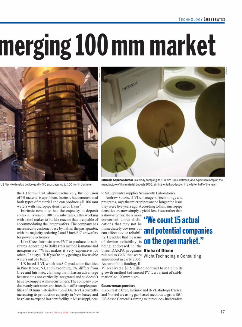
US-based Intrinsic Semiconductor, like Cree, isvertically integrated and can fabricate prototypedevices for customers. The company has already startedsampling 100 mm substrates and plans to offer pro-duction material in the current quarter. It is aiming forfull production in the latter half of the year. The com-pany’s current claim to fame, however, is producingsubstrates with a very low micropipe density.
A few years ago micropipes were the major defectworrying device manufacturers, but efforts to reducetheir incidence have resulted in lower densities acrossthe board. In late 2005 Intrinsic announced that it hadproduced 3 inch wafers completely free of any micro-pipes. Other defects are also important, however. Dixonpoints out that basal plane dislocations (which are crit-ical for PIN diodes), as well as inclusions of differentSiC polytypes, and chips and scratches accrued duringthe dicing process, can all degrade device performance.
Intrinsic CEO Cengiz Balkas says that his companyis focused on providing high-quality materials, withan intense effort on reducing basal plane dislocations.He agrees that controlling polytype uniformity is alsoimportant. Because power electronic devices require
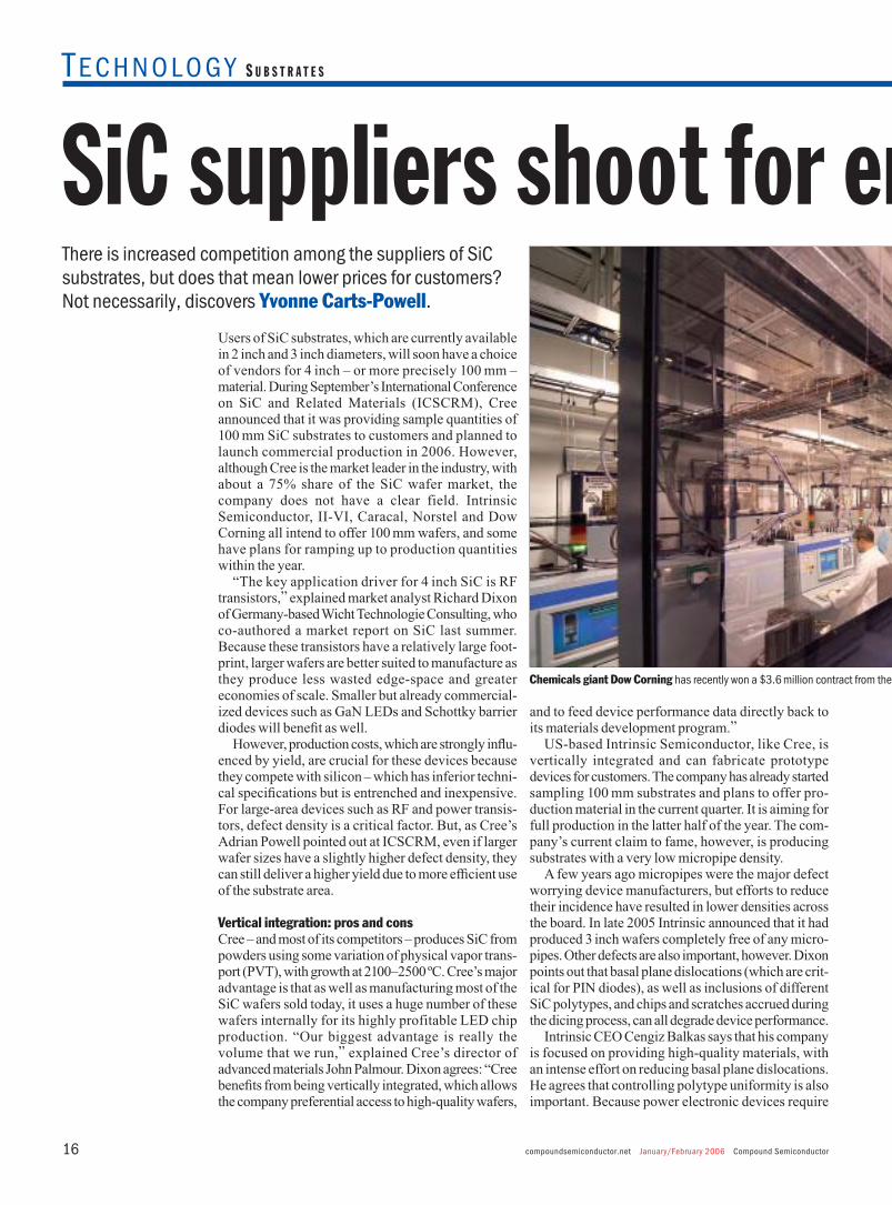
Chemicals giant Dow Corning has recently won a $3.6 million contract from the
Compound Semiconductor January/February 2006 compoundsemiconductor.net 17
TECHNOLOGY S U B S T R A T E S
the 4H form of SiC almost exclusively, the inclusionof 6H material is a problem. Intrinsic has demonstratedboth types of material and can produce 4H 100 mmwafers with micropipe densities of 1/ cm–2.
Intrinsic now also has the capacity to depositepitaxial layers on 100 mm substrates, after workingwith a tool maker to build a reactor that is capable ofaccommodating the larger wafers. The company hasincreased its customer base by half in the past quarter,with the majority ordering 2 and 3 inch SiC epiwafersfor power electronics.
Like Cree, Intrinsic uses PVT to produce its sub-strates. According to Balkas this method is mature andinexpensive. “What makes it very expensive forothers,” he says, “is if you’re only getting a few usablewafers out of a batch.”
US-based II-VI, which has SiC production facilitiesin Pine Brook, NJ, and Saxonburg, PA, differs fromCree and Intrinsic, claiming that it has an advantagebecause it is not vertically integrated and so doesn’thave to compete with its customers. The company pro-duces only substrates and intends to offer sample quan-tities of 100mm material by mid-2006. II-VI is currentlyincreasing its production capacity in New Jersey andhas plans to expand in a new facility in Mississippi, near
to SiC epiwafer supplier Semisouth Laboratories. Andrew Souzis, II-VI’s manager of technology and
programs, says that micropipes are no longer the issuethey were five years ago. According to him, micropipedensities are now simply a yield-loss issue rather thana show-stopper. He is moreconcerned about dislo-cations that may not beimmediately obvious butcan affect device reliabil-ity. He added that the issueof device reliability isbeing addressed in thethree DARPA programsrelated to GaN that wereannounced in early 2005.As part of this funding, II-VI received a $7.5 million contract to scale up itsgrowth method (advanced PVT, a variant of subli-mation) to 100 mm sizes.
Gases versus powdersIn contrast to Cree, Intrinsic and II-VI, start-ups Caracaland Norstel are using gas-based methods to grow SiC.US-based Caracal is aiming to introduce 4 inch wafers
merging 100mm market
US Navy to develop device-quality SiC substrates up to 100 mm in diameter.
DO
W C
OR
NIN
G C
OM
PO
UN
D S
EM
ICO
ND
UC
TOR
Intrinsic Semiconductor is already sampling its 100 mm SiC substrates, and expects to ramp up the
manufacture of this material through 2006, aiming for full production in the latter half of the year.
INTR
INS
IC
“We count 15 actual and potential companies on the open market.”Richard DixonWicht Technologie Consulting
compoundsemiconductor.net January/February 2006 Compound Semiconductor18
TECHNOLOGY S U B S T R A T E S
to the market in 2006. The company is focusing on theproduction of 4H conducting material for the powerelectronics market, but it can also grow 6H and semi-insulating wafers.
Jerry Connelly, Caracal’s chief marketing officer,claims that methods like seeded sublimation facechallenges with respect to quality and growth rate,which result in the high cost of today’s wafers. “Theadvantages of gas-based growth include the inherentpurity of the gases, greater control over the sublima-tion process, and the ability to cover pre-existing cracksin material, leading to higher-quality wafers,” heexplained. Similarly, Norstel CEO Asko Vehanenclaims that his company’s process has advantages overseed sublimation. These improvements include bettercontrol of purity, a more stable chemical compositionof gases at the crystalline interface, a more stable tem-perature distribution and a better control of growthgeometry during the single-crystal growth process.
Norstel uses a high-temperature CVD growthmethod developed at Linköping University in Sweden.In 2006 its new plant in Norrköping will become oper-ational, producing 3 inch wafers initially. The 100 mmwafers, says Vehanen, will be available in small vol-umes during 2007, and in large volumes the followingyear. The company produces both substrates andepitaxial wafers for customers worldwide.
The giant US chemicals company Dow Corning
recently won a $3.6 million contract from the US Navyto develop SiC, saying that it would use this funding todevelop a manufacturing capability for producingdevice-quality SiC substrates up to 100 mm in diame-ter. Dow’s global director of new business developmentprograms Robert Johns declined to specify when itmight enter the 100mm market, but claimed that Dow’sinfrastructure and its ability to provide both epiwafersand substrates gives it a competitive advantage.
An unsustainable supply baseGiven the size of the market, there is currently an unsus-tainable number of SiC suppliers. In the US the gov-ernment is providing contracts and support to Cree,Dow Corning, II-VI and Intrinsic, which improves theirchances of success, while Norstel also enjoys supportfrom the Swedish government, but in all these casesthe funding will not continue for ever.
“We count 15 actual and potential companies on theopen market, and others such as Toshiba that have imple-mented their own production lines for captive use,” saidDixon. However, many of these companies are not capa-ble of producing substrates in sizes as large as 3 inchesor 100 mm. Dixon added: “Although we expect thatincreased competition will contribute to a lowering ofwafer prices, in the current absence of a process to cost-effectively manufacture large SiC wafers, this [reduc-tion in costs] would be marginal.”
About the authorYvonne Carts-Powell is afreelance science writer basedin Belmont, MA, whospecializes in photonics,imaging, microtechnology andnanotechnology. [email protected].
Benefit fromreprints of articlesfeaturing yourcompanyReprints are invaluable sales tools
They can be ordered before or afterpublication and can be customized to your exact needs. For more information and prices, contact the sales team now.
Tel: +44 (0)117 930 1028
E-mail: [email protected]
Be part of your community
2006 INTERNATIONAL CONFERENCE ON COMPOUND SEMICONDUCTOR
MANUFACTURING TECHNOLOGY April 24-27, 2006
Fairmont Hotel Vancouver -- Vancouver, BC, CAN www.csmantech.org
Technical Sessions covering topics such
as Substrates and Epitaxy, Processing, Manufacturing Practices, CS Devices, Wide Bandgap, and Opto technologies.
Intensive multi-topic Workshop the day
before the conference opens.
Invited Papers that cover a range of topics from current and emerging technologies to “killer” applications.
Exhibits, presenting everything from
substrates to systems, provides a forum to meet directly with vendors.
Fairmont Hotel Vancouver
We will meet in the beautiful city of Vancouver, BC, well known for its international flair and vitality
www.tourismvancouver.com
Exhibitors' Forum, special lunch-time parallel sessions where vendors inform about their latest and greatest products.
The Interactive Forum, unique to CS
MANTECH, where conference attendees can engage in discussions with Technical Session authors and with each other.
Receptions, such as Exhibits Reception
and the International Reception provide opportunities for attendees to develop business contacts and network with colleagues in the industry.
Join us at the 21st Edition of the Premier Conference for Compound Semiconductor Manufacturing
For Additional Information and Advance Program please visit us at www.csmantech.org
Compound Semiconductor January/February 2006 compoundsemiconductor.net 21
T ECHNOLOGY T R A N S I S T O R S
High-power GaN HEMTs battlefor vacuum-tube territory
The market for millimeter-wave power amplifiersincludes applications in military, commercial and con-sumer sectors. The armed forces use the devices intransmitters for the detection of small targets and tar-get imaging, in radar equipment, communications andsmart weapons systems. In the commercial sector theamplifiers are widely used in high-data-rate commu-nication systems such as digital radio links, SATCOMand wireless LAN, while the consumer market isexpected to turn to millimeter-wave systems for appli-cations such as automotive radar.
Vacuum tubes are used in the vast majority of high-power amplifiers operating at millimeter-wave fre-quencies. However, this incumbent technology is underthreat from solid-state power amplifiers (SSPAs) thatare smaller, cheaper, more reliable and quicker to build.
Although these SSPAs could be constructed fromGaAs and InPHEMTs, these devices can only operateat low voltages and low powers. These limitations meanthat multiple amplifiers or MMICs must be combinedin order to deliver the output powers required, whichleads to highly complex systems operating at relativelylow efficiencies. GaN HEMTs can deliver high pow-ers at higher voltages, and promise simple, efficientmillimeter-wave power amplifiers.
Traps and other obstaclesGaN HEMTs are clearly excellent devices on paper.However, in practice they can suffer from high trapdensities, and at millimeter-wave frequencies their per-formance can be adversely affected by insufficientlylow channel resistance and poor pinch-off character-istics (a relatively large gate voltage is required to extin-guish the drain current).
High trap densities are exacerbated by the largestrain and high polarization charges in the AlGaN/GaNstructures. The trapping effect severely reduces AC
current under large-signal operation, and subsequentlydeteriorates the output power and efficiency.
At the relatively high millimeter-wave frequencies,to maintain an acceptable power output it is essentialto achieve a low channel resistance while maintaininggood pinch-off characteristics as the device gate lengthshrinks. Low channel resistance results from a highvalue for the product of the charge density and mobil-ity. However, if the charge density of the 2DEG isincreased by raising the aluminum content in theAlGaN layer, alloy scattering also increases, whichdegrades the mobility and consequently compromisesthe charge-mobility product.
Vacuum tubes are currentlyused in many radar systems, butthe US military has pumpedmillions of dollars of researchmoney into the development ofsolid-state GaN devices, whichwill be smaller, cheaper, morereliable and quicker to build.
The vacuum tubes used in today’smillimeter-wave transmitters face anincreasing threat from GaN HEMTs. Cree’s Yifeng Wu and Primit Parikh areleading the GaN charge with designs thatincorporate field plates, iron-dopedbuffer layers and a thin AlN interlayer todeliver a record power at 30 GHz.
US
NAV
Y
compoundsemiconductor.net January/February 2006 Compound Semiconductor22
TECHNOLOGY T R A N S I S T O R S
The pinch-off characteristics are related to the energyof the Fermi level of the GaN buffer layer below theactive channel. Although this Fermi level can beincreased by adding p-type dopants or other impuri-ties, this action also creates unwanted drain lags thatare attributed to buffer traps.
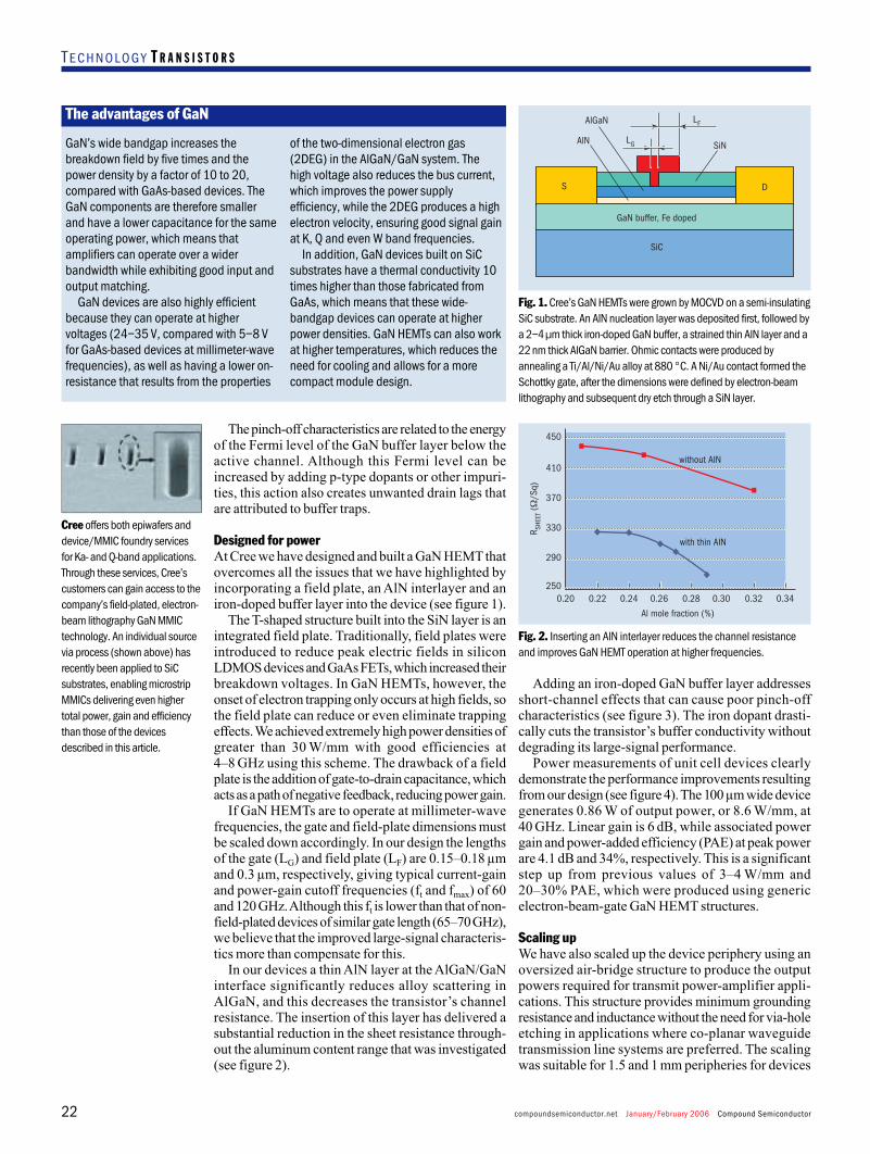
Designed for powerAt Cree we have designed and built a GaN HEMT thatovercomes all the issues that we have highlighted byincorporating a field plate, an AlN interlayer and aniron-doped buffer layer into the device (see figure 1).
The T-shaped structure built into the SiN layer is anintegrated field plate. Traditionally, field plates wereintroduced to reduce peak electric fields in siliconLDMOS devices and GaAs FETs, which increased theirbreakdown voltages. In GaN HEMTs, however, theonset of electron trapping only occurs at high fields, sothe field plate can reduce or even eliminate trappingeffects. We achieved extremely high power densities ofgreater than 30 W/mm with good efficiencies at4–8 GHz using this scheme. The drawback of a fieldplate is the addition of gate-to-drain capacitance, whichacts as a path of negative feedback, reducing power gain.
If GaN HEMTs are to operate at millimeter-wavefrequencies, the gate and field-plate dimensions mustbe scaled down accordingly. In our design the lengthsof the gate (LG) and field plate (LF) are 0.15–0.18 µmand 0.3 µm, respectively, giving typical current-gainand power-gain cutoff frequencies (ft and fmax) of 60and 120 GHz. Although this ft is lower than that of non-field-plated devices of similar gate length (65–70GHz),we believe that the improved large-signal characteris-tics more than compensate for this.
In our devices a thin AlN layer at the AlGaN/GaNinterface significantly reduces alloy scattering inAlGaN, and this decreases the transistor’s channelresistance. The insertion of this layer has delivered asubstantial reduction in the sheet resistance through-out the aluminum content range that was investigated(see figure 2).
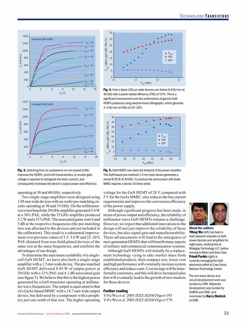
Adding an iron-doped GaN buffer layer addressesshort-channel effects that can cause poor pinch-offcharacteristics (see figure 3). The iron dopant drasti-cally cuts the transistor’s buffer conductivity withoutdegrading its large-signal performance.
Power measurements of unit cell devices clearlydemonstrate the performance improvements resultingfrom our design (see figure 4). The 100µm wide devicegenerates 0.86 W of output power, or 8.6 W/mm, at40 GHz. Linear gain is 6 dB, while associated powergain and power-added efficiency (PAE) at peak powerare 4.1 dB and 34%, respectively. This is a significantstep up from previous values of 3–4 W/mm and20–30% PAE, which were produced using genericelectron-beam-gate GaN HEMT structures.
Scaling upWe have also scaled up the device periphery using anoversized air-bridge structure to produce the outputpowers required for transmit power-amplifier appli-cations. This structure provides minimum groundingresistance and inductance without the need for via-holeetching in applications where co-planar waveguidetransmission line systems are preferred. The scalingwas suitable for 1.5 and 1 mm peripheries for devices
Cree offers both epiwafers anddevice/MMIC foundry servicesfor Ka- and Q-band applications.Through these services, Cree’scustomers can gain access to thecompany’s field-plated, electron-beam lithography GaN MMICtechnology. An individual sourcevia process (shown above) hasrecently been applied to SiCsubstrates, enabling microstripMMICs delivering even highertotal power, gain and efficiencythan those of the devicesdescribed in this article.
AlGaN
AlN SiN
LF
LG
GaN buffer, Fe doped
SiC
S D
Fig. 1. Cree’s GaN HEMTs were grown by MOCVD on a semi-insulatingSiC substrate. An AlN nucleation layer was deposited first, followed bya 2–4µm thick iron-doped GaN buffer, a strained thin AlN layer and a22nm thick AlGaN barrier. Ohmic contacts were produced byannealing a Ti/Al/Ni/Au alloy at 880°C. A Ni/Au contact formed theSchottky gate, after the dimensions were defined by electron-beamlithography and subsequent dry etch through a SiN layer.
0.32 0.340.300.280.260.240.220.20
450
410
370
330
290
250
R SHEE
T (Ω
/Sq)
without AIN
with thin AIN
Al mole fraction (%)
Fig. 2. Inserting an AlN interlayer reduces the channel resistanceand improves GaN HEMT operation at higher frequencies.
GaN’s wide bandgap increases thebreakdown field by five times and thepower density by a factor of 10 to 20,compared with GaAs-based devices. TheGaN components are therefore smallerand have a lower capacitance for the sameoperating power, which means thatamplifiers can operate over a widerbandwidth while exhibiting good input andoutput matching.
GaN devices are also highly efficientbecause they can operate at highervoltages (24–35 V, compared with 5–8 Vfor GaAs-based devices at millimeter-wavefrequencies), as well as having a lower on-resistance that results from the properties
of the two-dimensional electron gas(2DEG) in the AlGaN/GaN system. Thehigh voltage also reduces the bus current,which improves the power supplyefficiency, while the 2DEG produces a highelectron velocity, ensuring good signal gainat K, Q and even W band frequencies.
In addition, GaN devices built on SiCsubstrates have a thermal conductivity 10times higher than those fabricated fromGaAs, which means that these wide-bandgap devices can operate at higherpower densities. GaN HEMTs can also workat higher temperatures, which reduces theneed for cooling and allows for a morecompact module design.
The advantages of GaN
Compound Semiconductor January/February 2006 compoundsemiconductor.net 23
TECHNOLOGY T R A N S I S T O R S
operating at 30 and 40 GHz, respectively.Two single-stage amplifiers were designed using
1.05mm wide devices with on-wafer pre-matching cir-cuits operating at 30 and 35 GHz. On the millimeter-wave test bench the 30 GHz amplifier generated 5.4 Wat a 36% PAE, while the 35 GHz amplifier produced5.2 Wand a 31% PAE. The associated gains were 6 and5 dB at the respective frequencies (the pre-matchingloss was allocated to the devices and not included inthe calibration). This result is a substantial improve-ment over previous values of 3.5–3.6 W and 22–26%PAE obtained from non-field-plated devices of thesame size at the same frequencies, and confirms theadvantages of our design.
To determine the maximum scalability of a single-cell GaN HEMT, we have also built a single-stageamplifier with a 1.5 mm wide device. The pre-matchedGaN HEMT delivered 8.05 W of output power at30 GHz with a 31% PAE and 4.1 dB associated gain(see figure 5). We believe that this is the highest powergenerated by a GaN transistor operating at millime-ter-wave frequencies. The output is equivalent to thatof a GaAs-based MMIC with a 14.7 mm wide outputdevice, but delivered by a component with a periph-ery just one-tenth of that size. The higher operating
voltage for the GaN HEMT of 28 V, compared with5 V for the GaAs MMIC, also reduces the bus currentrequirements and improves the conversion efficiencyof the power supply.
Although significant progress has been made, interms of power output and efficiency, the reliability ofmillimeter-wave GaN HEMTs remains a challenge.However, we expect that additional innovations to thedesign will not just improve the reliability of thesedevices, but also signal gain and manufacturability.These advancements will lead to the emergence ofnext-generation HEMTs that will benefit many aspectsof military and commercial communication systems.
Although GaN HEMTs will initially be a replace-ment technology vying to take market share fromestablished products, their compact size, lower costand high performance will eventually increase systemefficiency and reduce costs. Cost savings will be trans-ferred to customers, and this will drive increased salesthat will eventually lead to the growth of new marketsfor these devices.
Further readingY-Fu Wu et al. 2005 IEEE IEDM Digest 193Y-Fu Wu et al. 2003 IEEE IEDM Digest 579.
About the authorsYifeng Wu (left) has been alead research scientist on GaNpower devices and amplifiers foreight years, working first atWidegap Technology LLC, beforemoving to Nitres and then Cree.Primit Parikh (right) iscurrently managing the GaNelectronics effort at Cree SantaBarbara Technology Center.
35
30
25
20
15
10
5
012 17 22 27
PIN (dBm)
P OUT (d
Bm),
gain
(dB)
, PAE
(%)
POUTPAEgain
1400
1200
1000
800
600
400
200
00 3 6 9 12 15 18
I D (m
A/m
m)
1400
1200
1000
800
600
400
200
00 3 6 9 12 15 18
VGS = 0V
VGS = –1V
VGS = –2V
VGS = –3V
VGS = –4V
VGS = –5V
VGS = –6VVGS = –7V
VGS = 0V
VGS = –1V
VGS = –2V
VGS = –3V
VGS = –4VVGS = –5V
I D (m
A/m
m)
VD (V)
VD (V)
undoped GaN buffer
Fe-doped GaN buffer
Fig. 3. Switching from an undoped to an iron-doped bufferimproves the HEMTs’ pinch-off characteristics (a smaller gatevoltage is required to extinguish the drain current), andconsequently increases the device’s output power and efficiency.
P OUT (d
Bm),
gain
(dB)
, PAE
(%)
40
35
30
25
20
15
10
5
023 25 27 29 31 33 35 37
PIN (dBm)
POUT
PAEgain
Fig. 4. Cree’s latest 100 µm wide devices can deliver 8.6 W/mm at40 GHz with a power-added efficiency (PAE) of 34%. This is asignificant improvement over the performance of generic GaNHEMTs produced using electron-beam lithography, which generate3–4 W/mm at PAEs of 20–30%.
Fig. 5. GaN HEMTs can slash the footprint of the power amplifier.This GaN-based pre-matched 1.5 mm wide device generates arecord 8.05 W at 30 GHz. To produce the same power with GaAsMMIC requires a device 10 times wider.
The mm-wave device andcircuit development work wasfunded by ONR. Materialsdevelopment was funded byDARPA and ONR, andmonitored by Harry Dietrichat ONR.
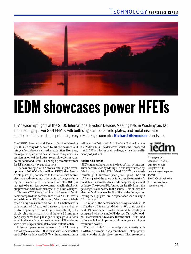
Compound Semiconductor January/February 2006 compoundsemiconductor.net 25
T ECHNOLOGY C O N F E R E N C E R E P O R T
IEDM showcases power HFETsIII-V device highlights at the 2005 International Electron Devices Meeting held in Washington, DC,included high-power GaN HEMTs with both single and dual field plates, and metal-insulator-semiconductor structures producing very low leakage currents. Richard Stevenson rounds up.
The IEEE’s International Electron Devices Meeting(IEDM) is always dominated by silicon devices, andthis year’s conference proved no exception. However,the organizing committee also chose to squeeze in asession on one of the hottest research topics in com-pound semiconductors – GaN high-power transistorsfor RF and microwave applications.
The session began with Nitronex detailing the devel-opment of 368 W GaN-on-silicon HFETs that featurea field plate (FP) connected to the transistor’s sourceelectrode and extending to the center of the gate–drainregion. The addition of this source field plate (SFP) isthought to be a critical development, enabling high out-put power and drain efficiency at high drain voltages.
Nitronex CTO Kevin Linthicum and a team of engi-neers compared the performance of GaN HFETs withand without an FP. Both types of device were fabri-cated on high-resistance silicon (111) substrates withgate lengths of 0.7 µm, and gate-to-source and gate-to-drain spacings of 1 and 3 µm, respectively. Thesingle-chip transistors, which have a 36 mm gateperiphery, were then packaged using a gold–siliconeutectic die attach in industry-standard RF packageswith a two-stage input match and no output match.
Pulsed RF power measurements at 2.14 GHz usinga 1% duty cycle and a 300 µs pulse width showed thatthe SFPdevice delivered 368Wwith a maximum drain
efficiency of 70% and 17.5 dB of small signal gain ata 60Vdrain bias. The device without the SFPproducedjust 225 W at a lower drain voltage, with a drain effi-ciency of just 33%.
Adding field platesNEC engineers have taken the idea of improving tran-sistor performance by adding FPs one stage further, byfabricating an AlGaN/GaN dual FP FET on a semi-insulating SiC substrate (see figure 1, p26). The firstFPforms part of the gate and improves the transistor’sbreakdown characteristics while suppressing currentcollapse. The second FP, formed on the SiN film at thegate edge, is connected to the source. This shields theelectric field between the first FP and the drain, elim-inating the high gate–drain capacitance seen in singleFP structures.
Comparing the performance of single and dual FPFETs, the NEC team found that at a 40 V drain bias thedual FPtransistor delivered an extra 3 dB of stable gaincompared with the single FP device. On-wafer load-pull measurements revealed that the dual FP FET hadwider stable load impedance, allowing easy tuning atmaximum power.
The dual FPFETalso showed greater linearity, witha 5dB improvement in adjacent channel leakage powerratio over the single-plate versions. The researchers
Washington, DC, December 5–7, 2005Organized by: IEEEDelegates: 1730Technical sessions/papers:41/240IEDM 2006 will be held in San Francisco, CA, onDecember 11–13
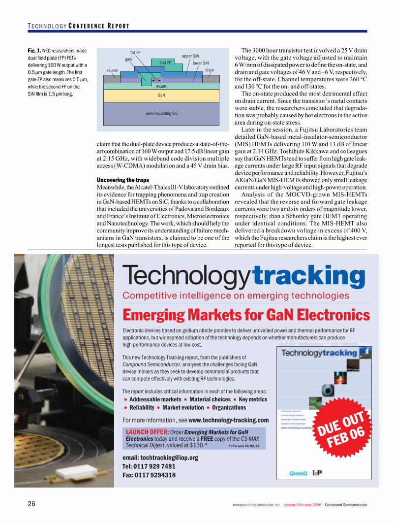
compoundsemiconductor.net January/February 2006 Compound Semiconductor26
TECHNOLOGY C O N F E R E N C E R E P O R T
claim that the dual-plate device produces a state-of-the-art combination of 160Woutput and 17.5dB linear gainat 2.15 GHz, with wideband code division multipleaccess (W-CDMA) modulation and a 45 V drain bias.
Uncovering the trapsMeanwhile, the Alcatel-Thales III-Vlaboratory outlinedits evidence for trapping phenomena and trap creationin GaN-based HEMTs on SiC, thanks to a collaborationthat included the universities of Padova and Bordeauxand France’s Institute of Electronics, Microelectronicsand Nanotechnology. The work, which should help thecommunity improve its understanding of failure mech-anisms in GaN transistors, is claimed to be one of thelongest tests published for this type of device.
The 3000 hour transistor test involved a 25 V drainvoltage, with the gate voltage adjusted to maintain6 W/mm of dissipated power to define the on-state, anddrain and gate voltages of 46 V and –6 V, respectively,for the off-state. Channel temperatures were 260 °Cand 130 °C for the on- and off-states.
The on-state produced the most detrimental effecton drain current. Since the transistor’s metal contactswere stable, the researchers concluded that degrada-tion was probably caused by hot electrons in the activearea during on-state stress.
Later in the session, a Fujitsu Laboratories teamdetailed GaN-based metal-insulator-semiconductor(MIS) HEMTs delivering 110 W and 13 dB of lineargain at 2.14 GHz. Toshihide Kikkawa and colleaguessay that GaN HEMTs tend to suffer from high gate leak-age currents under large RF input signals that degradedevice performance and reliability. However, Fujitsu’sAlGaN/GaN MIS-HEMTs showed only small leakagecurrents under high-voltage and high-power operation.
Analysis of the MOCVD-grown MIS-HEMTsrevealed that the reverse and forward gate leakagecurrents were two and six orders of magnitude lower,respectively, than a Schottky gate HEMT operatingunder identical conditions. The MIS-HEMT alsodelivered a breakdown voltage in excess of 400 V,which the Fujitsu researchers claim is the highest everreported for this type of device.
Competitive intelligence on emerging technologies
TechnologytrackingEmerging Markets for GaN ElectronicsElectronic devices based on gallium nitride promise to deliver unrivalled power and thermal performance for RFapplications, but widespread adoption of the technology depends on whether manufacturers can produce high-performance devices at low cost.
This new Technology Tracking report, from the publishers of Compound Semiconductor, analyses the challenges facing GaN device makers as they seek to develop commercial products that can compete effectively with existing RF technologies.
The report includes critical information in each of the following areas:
• Addressable markets • Material choices • Key metrics • Reliability • Market evolution • Organizations
For more information, see www.technology-tracking.com
DUE OUT
FEB 06LAUNCH OFFER: Order Emerging Markets for GaNElectronics today and receive a FREE copy of the CS-MAXTechnical Digest, valued at $150.* *Offer ends 28/02/06
email: [email protected]: 0117 929 7481Fax: 0117 9294318
Fig. 1. NEC researchers madedual field plate (FP) FETsdelivering 160 W output with a0.5 µm gate length. The firstgate FP also measures 0.5 µm,while the second FP on the SiN film is 1.5 µm long.
gate
GaN
AlGaN
source
upper SiN
lower SiN
drain
1st FP
semi-insulating SiC
2nd FP
Compound Semiconductor January/February 2006 compoundsemiconductor.net 27
T ECHNOLOGY L A S E R S
Shallow etch could power dilute-nitride VCSEL breakthrough
Multimode VCSELs operating at 850 nm are thedominant source for today’s short-range datacomapplications. However, despite advantages such as on-chip testing and straightforward fiber coupling,these surface-emitting devices are still to impact the longer range and higher speed datacom and telecom applications.
Infineon Technologies, Picolight and OpticalCommunication Products have all developed 1.3 µmVCSELs, but their single-mode output powers arelimited, and this has hindered market penetration inmore demanding applications. Instead, current net-works are served with edge-emitting sources – eitherFabry–Pérot lasers that are limited in range by modaldispersion at higher modulation frequencies, ordistributed-feedback lasers that usually require anadditional optical isolator.
However, recent efforts at our company, AlightTechnologies, have revealed that a VCSEL’s single-mode output power can be increased to fulfill therequirements of communications applications throughthe addition of a photonic-bandgap (PBG) structure.Our team, which is based in Copenhagen, Denmark,has made the breakthrough by combining this photonictechnology with Infineon’s 1.3 µm dilute-nitrideVCSEL design, which we acquired late last year.
The single-mode output of a conventional VCSELis primarily limited by the oxide aperture that confinesthe electrical current and the optical modes. This aper-ture has to be quite small (<7 µm) to ensure funda-mental-mode operation, but this restriction limits theoutput power. It also degrades the laser’s lifetime andreliability, while the large electrical resistance causeslocal heating and hinders high-speed operation.
However, our colleague Svend Bischoff, who is asenior staff engineer at Alight, has reported that it is pos-
sible to produce high-speed, high-power single-modeVCSELs by combining a PBG structure for lateral opti-cal confinement with a large oxide aperture providingcurrent confinement. The PBG is formed by etching anarray of holes in the VCSEL’s top mirror. The modifiedstructure produces a wavelength shift in the cavity res-onance that leads to an effective refractive-indexchange, and this produces the lateral optical mode con-finement that ensures single-mode operation.
Etching effectsThe shift in cavity resonance wavelength is very smallfor shallow etch depths of a few hundred nanometersinto the VCSEL’s top-mirror surface, so the VCSELsfabricated up until now – at the University of Ulm inGermany and Korea’s Advanced Institute of Scienceand Technology – have featured holes with a depth of10–20 mirror periods. The holes deliver the requiredshift in cavity resonance wavelength, but also increasethe optical losses and reduce the photon lifetime (theaverage time that photons spend in the cavity). Thismeans that these lasers have low output powers and asmall modal volume because the lateral mode con-finement is determined by both the photon lifetime andthe shift in cavity resonance wavelength.
Alight Technologies is tackling the needfor powerful long-wavelength, single-mode VCSELs by marrying its photonic-bandgap technology with Infineon’sdilute-nitride platform. Dan Birkedaland Dirk Jessen detail the hybriddesign and reveal why it will benefitdatacom and telecom networks.
Incorporating a photonicbandgap structure into a dilutenitride VCSEL increases itssingle-mode output power andenables it to compete with theFabry–Pérot and distributed-feedback lasers that are servingtoday’s networks.
PHO
TOD
ISC
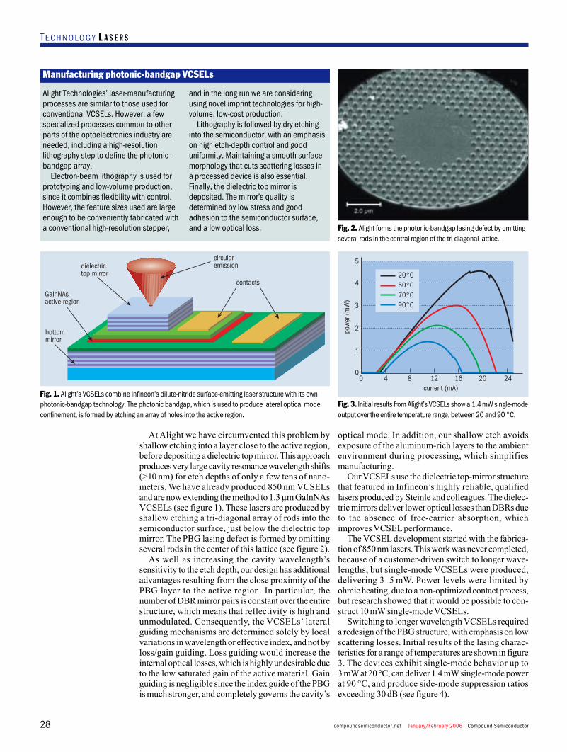
compoundsemiconductor.net January/February 2006 Compound Semiconductor28
TECHNOLOGY L A S E R S
At Alight we have circumvented this problem byshallow etching into a layer close to the active region,before depositing a dielectric top mirror. This approachproduces very large cavity resonance wavelength shifts(>10 nm) for etch depths of only a few tens of nano-meters. We have already produced 850 nm VCSELsand are now extending the method to 1.3 µm GaInNAsVCSELs (see figure 1). These lasers are produced byshallow etching a tri-diagonal array of rods into thesemiconductor surface, just below the dielectric topmirror. The PBG lasing defect is formed by omittingseveral rods in the center of this lattice (see figure 2).
As well as increasing the cavity wavelength’ssensitivity to the etch depth, our design has additionaladvantages resulting from the close proximity of thePBG layer to the active region. In particular, thenumber of DBR mirror pairs is constant over the entirestructure, which means that reflectivity is high andunmodulated. Consequently, the VCSELs’ lateralguiding mechanisms are determined solely by localvariations in wavelength or effective index, and not byloss/gain guiding. Loss guiding would increase theinternal optical losses, which is highly undesirable dueto the low saturated gain of the active material. Gainguiding is negligible since the index guide of the PBGis much stronger, and completely governs the cavity’s
optical mode. In addition, our shallow etch avoidsexposure of the aluminum-rich layers to the ambientenvironment during processing, which simplifiesmanufacturing.
Our VCSELs use the dielectric top-mirror structurethat featured in Infineon’s highly reliable, qualifiedlasers produced by Steinle and colleagues. The dielec-tric mirrors deliver lower optical losses than DBRs dueto the absence of free-carrier absorption, whichimproves VCSEL performance.
The VCSEL development started with the fabrica-tion of 850 nm lasers. This work was never completed,because of a customer-driven switch to longer wave-lengths, but single-mode VCSELs were produced,delivering 3–5 mW. Power levels were limited byohmic heating, due to a non-optimized contact process,but research showed that it would be possible to con-struct 10 mW single-mode VCSELs.
Switching to longer wavelength VCSELs requireda redesign of the PBG structure, with emphasis on lowscattering losses. Initial results of the lasing charac-teristics for a range of temperatures are shown in figure3. The devices exhibit single-mode behavior up to3mWat 20°C, can deliver 1.4mWsingle-mode powerat 90 °C, and produce side-mode suppression ratiosexceeding 30 dB (see figure 4).
Alight Technologies’ laser-manufacturingprocesses are similar to those used forconventional VCSELs. However, a fewspecialized processes common to otherparts of the optoelectronics industry areneeded, including a high-resolutionlithography step to define the photonic-bandgap array.
Electron-beam lithography is used forprototyping and low-volume production,since it combines flexibility with control.However, the feature sizes used are largeenough to be conveniently fabricated witha conventional high-resolution stepper,
and in the long run we are consideringusing novel imprint technologies for high-volume, low-cost production.
Lithography is followed by dry etchinginto the semiconductor, with an emphasison high etch-depth control and gooduniformity. Maintaining a smooth surfacemorphology that cuts scattering losses ina processed device is also essential.Finally, the dielectric top mirror isdeposited. The mirror’s quality isdetermined by low stress and goodadhesion to the semiconductor surface,and a low optical loss.
Manufacturing photonic-bandgap VCSELs
powe
r (m
W)
current (mA)0
1
2
3
4
5
04 8 12 16 20 24
20°C50°C70°C90°C
Fig. 3. Initial results from Alight’s VCSELs show a 1.4mW single-modeoutput over the entire temperature range, between 20 and 90°C.
dielectrictop mirror
GaInNAsactive region
circularemission
contacts
bottommirror
Fig. 1. Alight’s VCSELs combine Infineon’s dilute-nitride surface-emitting laser structure with its ownphotonic-bandgap technology. The photonic bandgap, which is used to produce lateral optical modeconfinement, is formed by etching an array of holes into the active region.
Fig. 2. Alight forms the photonic-bandgap lasing defect by omittingseveral rods in the central region of the tri-diagonal lattice.
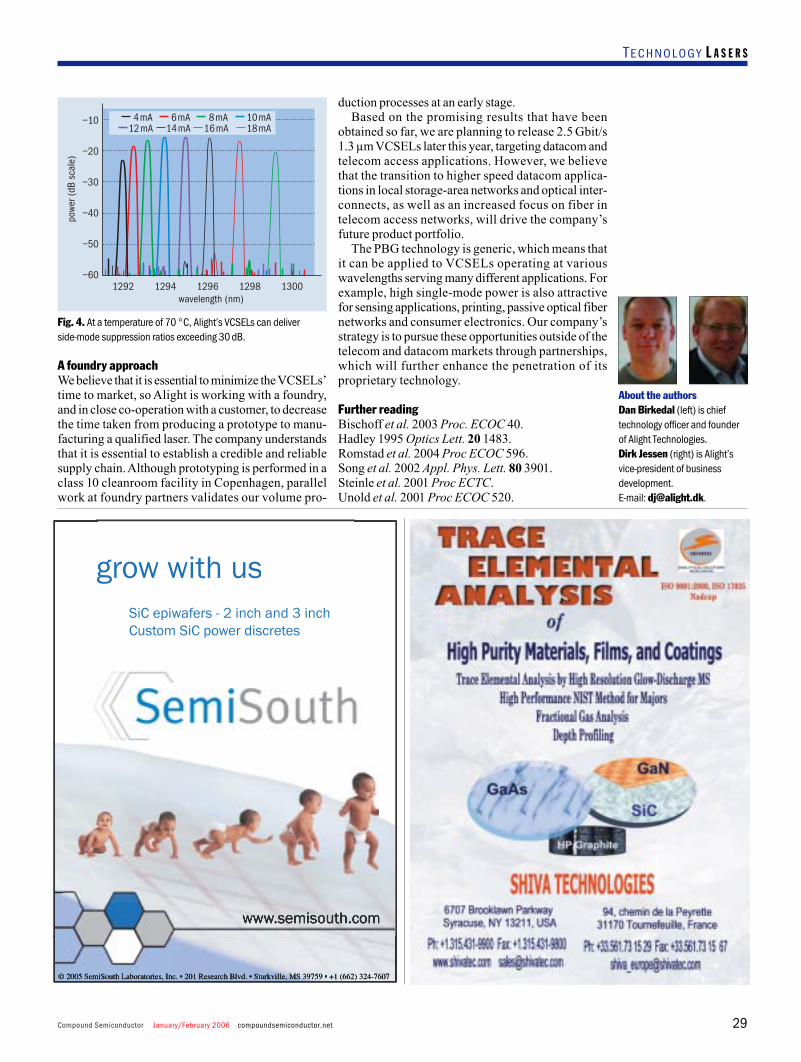
Compound Semiconductor January/February 2006 compoundsemiconductor.net 29
TECHNOLOGY L A S E R S
A foundry approachWe believe that it is essential to minimize the VCSELs’time to market, so Alight is working with a foundry,and in close co-operation with a customer, to decreasethe time taken from producing a prototype to manu-facturing a qualified laser. The company understandsthat it is essential to establish a credible and reliablesupply chain. Although prototyping is performed in aclass 10 cleanroom facility in Copenhagen, parallelwork at foundry partners validates our volume pro-
duction processes at an early stage.Based on the promising results that have been
obtained so far, we are planning to release 2.5 Gbit/s1.3 µm VCSELs later this year, targeting datacom andtelecom access applications. However, we believethat the transition to higher speed datacom applica-tions in local storage-area networks and optical inter-connects, as well as an increased focus on fiber intelecom access networks, will drive the company’sfuture product portfolio.
The PBG technology is generic, which means thatit can be applied to VCSELs operating at variouswavelengths serving many different applications. Forexample, high single-mode power is also attractivefor sensing applications, printing, passive optical fibernetworks and consumer electronics. Our company’sstrategy is to pursue these opportunities outside of thetelecom and datacom markets through partnerships,which will further enhance the penetration of itsproprietary technology.
Further readingBischoff et al. 2003 Proc. ECOC 40.Hadley 1995 Optics Lett. 20 1483.Romstad et al. 2004 Proc ECOC 596.Song et al. 2002 Appl. Phys. Lett. 80 3901.Steinle et al. 2001 Proc ECTC.Unold et al. 2001 Proc ECOC 520.
About the authorsDan Birkedal (left) is chieftechnology officer and founderof Alight Technologies. Dirk Jessen (right) is Alight’svice-president of businessdevelopment. E-mail: [email protected].
wavelength (nm)
powe
r (dB
sca
le)
1292 1294 1296 1298 1300–60
–50
–40
–30
–20
–10 4mA 6mA 8mA 10mA18mA16mA14mA12mA
Fig. 4. At a temperature of 70 °C, Alight’s VCSELs can deliver side-mode suppression ratios exceeding 30 dB.
grow with us
SiC epiwafers - 2 inch and 3 inch
Custom SiC power discretes
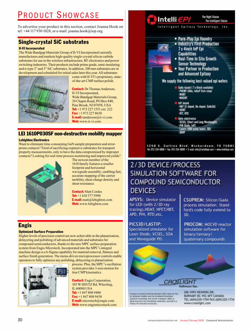
compoundsemiconductor.net January/February 2006 Compound Semiconductor30
PRODUCT SHOWCASE
Single-crystal SiC substratesII-VI IncorporatedThe Wide Bandgap Materials Group of II-VI Incorporated currentlymanufactures and markets high-quality single-crystal silicon carbidesubstrates for use in the wireless infrastructure, RF electronics and powerswitching industries. Their products include prime grade, semi-insulatingand n-type 2" and 3" SiC substrates. In addition, 100 mm substrates are indevelopment and scheduled for initial sales later this year. All substrates
come with II-VI’s proprietary, state-of-the-art CMP surface polish.
Contact: Dr Thomas Anderson, II-VI Incorporated, Wide Bandgap Materials Group, 20 Chapin Road, PO Box 840, Pine Brook, NJ 07058, USATel: +1 973 227 1551 ext. 222Fax: +1 973 227 8658E-mail: [email protected]: www.ii-vi.com
EngisOptimized Surface PreparationHigher levels of precision control are now achievable in the planarization,delayering and polishing of advanced materials and substrates forcompound semiconductors, thanks to the new MPC surface preparationsystem from Engis-Microtech. Incorporated into the MPC’s integralmachine design is a 6-Sigma capability for material removal, flatness andsurface finish generation. The menu-driven microprocessor controls enableoperators to fully optimize any polishing, delayering or planarization
process. Plus, the MPC’s oscillationsystem provides 3-axis motion fortrue CMP kinematics.
Contact: Engis Corporation, 105 W HINTZ Rd, Wheeling, IL 60090 USATel: +1 847 808 9400Fax: +1 847 808 9430E-mail: [email protected]: www.engismicrotech.com
LEI 1610P030SF non-destructive mobility mapperLehighton ElectronicsWant to eliminate time-consuming GaN sample preparation and error-prone contacts? Tired of sacrificing expensive substrates for transportproperty measurements, only to have the data compromised by impropercontacts? Looking for real-time process monitoring and improved yields?
The newest member of the1610 family features a smallerfootprint and horizontal waveguide assembly; enabling fast,accurate mapping of the carriermobility, sheet charge density andsheet resistance.
Contact: Matt Cordes Tel: +1 610 377 5990E-mail: [email protected]: www.lehighton.com
To advertise your product in this section, contact Joanna Hook on tel: +44 117 930 1028, or e-mail: [email protected].
Compound Semiconductor January/February 2006 compoundsemiconductor.net 31
T ECHNOLOGY E Q U I P M E N T U P D A T E
If the high-brightness LED is ever going to replace thelight bulb then its price-per-lumen will have to fall sub-stantially. Large savings could result if GaN LED chipmakers, which mainly grow their devices on 2 inch sap-phire substrates, switch to 4 inch material. However,growth on a foreign substrate causes strain in the GaNepilayers, and managing this strain is a real challengewith larger wafers. Yields suffer if the strain causes thewafer to bend, as any deformation produces a tempera-ture variation across the substrate that leads to inhomo-geneities in epilayer composition.
Although it is possible to produce LED epiwafers onlarge substrates, many growth runs are required to opti-mize the growth parameters that can cause the wafers tobend. This approach is both time-consuming and expen-sive, which is why Germany-based LayTec has recentlyreleased a sensor for MOCVD reactors that can moni-tor the wafer’s strain in situ. According to the companypresident Thomas Zettler, the EpiCurve reflectance sen-sor can slash the time and expense required to perfect astructure: “One customer used 80 runs to modify itsrecipe for blue LEDs, but for the next generation ofdevices [developed with an EpiCurve tool] only 20 runswill be necessary.” The sensor can also improve pro-duction efficiency, as it reveals whether the process stayswithin the limits required to produce an in-spec epiwafer.
EpiCurve can provide reflectance measurements dur-ing most stages of the growth of a typical LED, includ-ing deposition of AlGaN layers that typically have asurface roughness of a few nanometers. These mea-surements are unaffected by isolated defects on thewafer, as their contribution is filtered out by the soft-ware. However, the instrument cannot provide mean-ingful data during growth of the very rough GaNnucleation layer formed at the sapphire–GaN interface.
The sensor was developed a few years ago by AloisKroist’s research team at the Otto-von-Guericke Uni-versity, Magdeburg, Germany. It determines the strainby monitoring the changes in the separation of two 633nmlaser beams that are reflected from the epiwafer surface– convex and concave wafers are identified by laser spotseparation increasing and decreasing, respectively.
“The critical technological breakthrough was todevelop a small optical head that was able to measurethis effect through only a few millimeters of viewport,”says Zettler, who explained that space is severely lim-ited for monitoring equipment installed in MOCVDreactors. The EpiCurve can be fitted to the majority of
Aixtron’s single-wafer and planetary MOCVD machines– while Veeco’s reactors have their own brand of in situreflectance sensors that can be fitted to these machines.
Although LayTec’s EpiCurve sensor can readily deter-mine the wafer’s curvature during nearly all the LEDgrowth stages, it is unable to form part of an active feed-back system that could automatically adjust growth par-ameters in real time and maintain optimized conditionsduring a run. However, Zettler says that in a few yearsthe thickness of a strain engineering layer could be mod-ified by this kind of feedback control mechanism.
Most reactors used for LED manufacturing alreadyhave a port for other forms of in situ monitoring, so estab-lished growth recipes require no alteration after the addi-tion of an EpiCurve sensor. As the existing ports alreadyuse a flow of gas to prevent material growth over thisarea, the sensor can be used for many uninterrupted runs.
EpiCurve’s benefits will probably appeal to many fabmanagers, but they will have to weigh its advantagesagainst the downtime required to install the sensor ontothe reactor. However, Zettler believes that these man-agers should not be put off by the short delay to produc-tion: “For many, many customers the sensor will payback the effort within a few weeks.”
Although the largest target market is GaN LED chipmakers, the EpiCurve sensor is also suitable for GaN-on-silicon epitaxy. The prototype EpiCurve sensor builtat the Otto-von-Guericke University was actually con-structed for this purpose. Today this university’s newspin-off, Azzurro Semiconductors, is using the sensor tomanufacture crack-free GaN epiwafers of up to 150 mmin diameter, with GaN layers up to 5 µm thick.
Reflectance sensor eases the strain
LayTec’s EpiCurve sensor can be fitted to MOCVD reactors to determine the strain in GaN structuresgrown on sapphire, SiC and silicon substrates. The sensor helps to streamline product development.
M O C V D M O N I T O R
A new reflectance sensor from LayTec aids LEDdevelopment and manufacturing by providingin situ strain measurements of the epilayers.Richard Stevenson learns how German start-up Azzurro Semiconductors is using the sensorfor GaN-on-silicon growth.
“For many, manycustomers thesensor will pay backthe effort within afew weeks.”Thomas ZettlerLayTec
LAYTEC
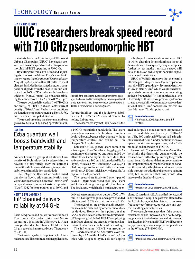
compoundsemiconductor.net January/February 2006 Compound Semiconductor32
T ECHNOLOGY R E S E A R C H R E V I E W
I n P T R A N S I S T O R S
Scientists from the University of Illinois atUrbana-Champaign (UIUC) have again bro-ken the transistor speed record with a pseudo-morphic InP HBT operating at 710 GHz.
By cutting the transistor’s size and adjust-ing its composition Milton Feng’s team brokeits own record (see Compound SemiconductorMay 2005 p6) by more than 100 GHz. Criticalchanges included increasing the indium com-positional grade from the base to the sub-col-lector from 16% to 21%, reducing the base layerthickness from 20 nm to 12.5 nm, and shrink-ing the emitter from 0.4 × 6 µm to 0.25 × 3 µm.
The new design delivered an fT of 710 GHzand an fmax of 340 GHz at a collector currentdensity of 20 mA/µm2. Under these conditionsthe junction temperature increased by 150 °C,and the device dissipated 14 mW.
The record-breaking transistor material wasgrown by MBE at US-based epiwafer manu-
facturer Intelliepi, and the device was fabri-cated at UIUC’s own Micro and Nanotech-nology Laboratory.
The researchers say that their device is the
first high-performance submicrometer HBTin which charging delays dominate the totaldevice delay. Consequently, any attempts atfurther increasing the transistor’s speed willhave to focus on reducing its parasitic capac-itances and resistances.
UIUC’s Walid Hafez says that the team’sultimate goal is to produce a terahertz pseudo-morphic HBToperating with current densitiesas low as 30 mA/µm2, which would aid devel-opment of communication systems operatingat these frequencies. “HBTs fabricated at theUniversity of Illinois have previously demon-strated the capability of running at current den-sities of 30 mA/µm2, so we know that this is afeasible target,” Hafez pointed out.
UIUC researchers break speed recordwith 710 GHz pseudomorphic HBT
Journal referenceW Hafez et al. 2005 Appl. Phys. Lett. 87252109.
Reducing the transistor’s overall size, thinning the baselayer thickness, and increasing the indium compositionalgrade from the base to the sub-collector contributed to a100GHz improvement in switching speed.
Anders Larsson’s group at Chalmers Uni-versity of Technology in Sweden claims tohave built dilute nitride lasers that deliver arecord threshold current density, temperaturestability and modulation bandwidth.
The 1.28 µm emitters, which could be usedone day in fiber-optic communication net-works, have a threshold current of 150mA/cm2
per quantum well, a characteristic temperature(T0) of 180 K for temperatures up to 70 °C, and
a 14 GHz modulation bandwidth. The lasershave advantages over the InP-based emittersdeployed today, because they operate withouttemperature control, and can be built oncheaper GaAs substrates.
Larsson’s MBE-grown lasers contain anactive region of two 7nm thick Ga0.613In0.387NAsquantum wells separated and surrounded by20 nm thick GaAs layers. Either side of thisactive region are 160 nm thick graded AlGaAslayers, followed by 1 µm thick Al0.5Ga0.5Ascladding regions doped with either silicon orberyllium. A100nm thick heavily doped GaAscap forms the top contact.
The researchers fabricated two types ofdevice: 100 µm wide broad-area (BA) lasersand 4 µm wide ridge waveguide (RW) lasers.The BAlasers, which had a 1 mm cavity, oper-
ated under pulse-mode at room temperaturewith a threshold current density of 300 mA/cm2. The 400 µm long RWlasers had a thresh-old current of 22 mA under continuous-waveoperation at room temperature, and a 3 dBmodulation bandwidth of 14 GHz.
Larsson told Compound Semiconductor thathe thinks the threshold current could bereduced even further by optimizing the growthconditions. He also said that improvements tothe temperature stability and modulation band-width especially at high temperatures are pos-sible through the addition of another quantumwell, but he warned that this would alsoincrease the threshold current.
Extra quantum wellboosts bandwidth andtemperature stability
L A S E R S
Journal referenceY Q Wei et al. 2005 Electron. Lett. 41 1328.
Farid Medjdoub and co-workers at France’sElectronics, Microelectronics and Nano-technology Institute in Villeneuve D’Ascqhave produced an InP channel HEMT with a0.1 µm gate that has a record cut-off frequencyof 94 GHz.
The transistor, which has potential for futureradar and satellite communication applications,
delivers a maximum power output of 200mW/mm, a 3.8 dB power gain, and a power addedefficiency of 13.7% at a drain voltage of 2.5 V.
The researchers are aware that this perfor-mance can be matched by other semiconduc-tor devices. However, they point out thatGaAs-based devices suffer from a limited cut-off frequency, while InP HEMTs employingan InGaAs channel are affected by impact ion-ization that reduces the breakdown voltage.
The InP channel HEMT was grown byMBE, and contains an AlInAs buffer layer, fol-lowed by a 12 nm thick InP channel, a 3 nmthick AlInAs spacer layer, a silicon doping
plane, 10 nm thick AlInAs and InPlayers, anda 20 nm InGaAs cap. The gate was attached tothe AlInAs layer, which is claimed to improvefrequency performance, power gain and cur-rent handling characteristics.
The research team says that if the contactresistances can be improved, and a double dop-ing plane is inserted to improve drain currentdensity, then InPchannel HEMTs will becomevery promising devices for power applicationsin the W-band (75–110 GHz).
InP channel deliversreliability at 94 GHz
H E M T D E V E L O P M E N T
Journal referenceF Medjdoub et al. 2005 Electron. Lett. 41 1406.
UIU
C

www.picogiga.com
Explore new frontiers in III-V performance. Rely on compound material
solutions from Picogiga International. Only Picogiga combines 20 years
of MBE expertise with the Soitec Group’s global resources and industry-
leading Smart Cut™ technology. Picogiga—your partner at the leading
edge of innovation. Just imagine the possibilities.
Picogiga International. A division of the Soitec Group.
B R E A K A W A Y

Solutions for a nanoscale world.™
For high-volume production of GaN-based HB LEDs, GaNzilla™ II sets the standard. GaNzilla II, Veeco’s next generation TurboDisc® reactor, improves LED yield and brightness. Plus, its unique loadlock design enables continuous operation for the highest throughput available today. Visit www.veeco.com/gan or call 1.888.24.VEECO to learn how GaNzilla II can improve your premium LED output.
Want more premium LEDsfrom your MOCVD system?
Introducing GaNzilla II: higher throughput,superior uniformity, brighter LEDs.
GaNzilla™ II MOCVD System
Compound Semiconductor SolutionsMBE, MOCVD, PVD, IBD, IBE,AFM and Optical MetrologyProcess Integration Center