Embed Size (px)
Citation preview

Computational Study of Metal Contacts to MonolayerTransition-Metal Dichalcogenide Semiconductors
Jiahao Kang,1 Wei Liu,1 Deblina Sarkar,1 Debdeep Jena,2 and Kaustav Banerjee11University of California, Santa Barbara, California 93106, USA2University of Notre Dame, Notre Dame, Indiana 46556, USA
(Received 27 June 2013; revised manuscript received 23 February 2014; published 14 July 2014)
Among various 2D materials, monolayer transition-metal dichalcogenide (mTMD) semiconductors withintrinsic band gaps (1–2 eV) are considered promising candidates for channel materials in next-generationtransistors. Low-resistance metal contacts to mTMDs are crucial because currently they limit mTMDdevice performances. Hence, a comprehensive understanding of the atomistic nature of metal contacts tothese 2D crystals is a fundamental challenge, which is not adequately addressed at present. In this paper, wereport a systematic study of metal-mTMD contacts with different geometries (top contacts and edgecontacts) by ab initio density-functional theory calculations, integrated with Mulliken population analysisand a semiempirical van der Waals dispersion potential model (which is critical for 2D materials and notwell treated before). Particularly, In, Ti, Au, and Pd, contacts to monolayer MoS2 and WSe2 as well asMo-MoS2 and W-WSe2 contacts are evaluated and categorized, based on their tunnel barriers, Schottkybarriers, and orbital overlaps. Moreover, going beyond Schottky theory, new physics in such contactinterfaces is revealed, such as the metallization of mTMDs and abnormal Fermi level pinning. Among thetop contacts to MoS2, Ti and Mo show great potential to form favorable top contacts, whichare both n-type contacts, while for top contacts to WSe2, W or Pd exhibits the most advantages as ann- or p-type contact, respectively. Moreover, we find that edge contacts can be highly advantageouscompared to top contacts in terms of electron injection efficiency. Our formalism and the results provideguidelines that would be invaluable for designing novel 2D semiconductor devices.
DOI: 10.1103/PhysRevX.4.031005 Subject Areas: Computational Physics, Electronics,Nanophysics
I. INTRODUCTION
As silicon complementary metal oxide semiconductortechnology approaches its limits in scaling, an alternativematerial to silicon is needed for future logic transistorapplications. 2D crystal semiconductors, with extremelysmall thicknesses (few Å), uniform band gap over a largearea, and pristine interfaces without out-of-plane danglingbonds, have the potential to allow efficient electrostatics,reduction of short channel effects, fewer traps on a semi-conductor-dielectric interface, and a high degree of verticalscaling (Fig. 1). Recently, many types of 2D materials,including graphene [1,2] and hexagonal boron nitride(h-BN) [3], have been experimentally and theoreticallydemonstrated. While these materials do not have the re-quisite band gaps (Eg) [graphene: 0 eV; h-BN: > 5 eV; seeFig. 2(a)] for use as channel materials in digital applica-tions, monolayer transition-metal dichalcogenide (mTMD)semiconductors, a family of 2D semiconductor monolayers
arranged in a hexagonal lattice [Figs. 2(b) and 2(c)], exhibitconsiderable Eg (1–2 eV) [Figs. 2(a), 2(d), and 2(e)],thereby presenting great potential for low-power digitalapplications [4–7]. The 2D TMD materials are alsoattractive for display electronics [8] due to their inherentflexibility, transparency, and dangling-bond-free interfacethat make them easy to integrate with various substrates.Moreover, field-effect-transistor (FET-)based biosensorswith 2D TMD semiconductor as the channel material haverecently been demonstrated [9] to be highly advantageousover all other nanomaterial-based (including graphene)FET biosensors, due to their atomically layered and planarnature, nonzero band gaps, and pristine surfaces.However, the formation of low-resistance metal contacts
is the biggest challenge that masks the innate exceptionalelectronic and magnetic properties of 2D semiconductors,due to their band gaps and pristine surfaces, as well as lackof proper doping approach. To overcome this issue, severalstudies on specific cases of metal-TMD contacts have beenreported recently: (1) Ti-MoS2 and Au-MoS2 top contacts[10] with the configuration shown in Fig. 3(a), whichare only qualitatively studied by density-functionaltheory (DFT) in the absence of the treatment of van derWaals (vdW) interaction (which will be discussed later);
Published by the American Physical Society under the terms ofthe Creative Commons Attribution 3.0 License. Further distri-bution of this work must maintain attribution to the author(s) andthe published article’s title, journal citation, and DOI.
PHYSICAL REVIEW X 4, 031005 (2014)
2160-3308=14=4(3)=031005(14) 031005-1 Published by the American Physical Society

(2) Sc, Ni, and Au contacts to multilayer MoS2 [11]; (3) Ticontacts to multilayer MoS2 [12]; (4) Pd-WSe2 contact [6];(5) In-, Al-, and Ag-WSe2 contact [7]; and (6) 2D com-pound metal contacts to MoS2 [13] studied by DFT.However, these works are not systematic and lack therigorousness necessary for accurate analysis. On the otherhand, the typical value of metal-mTMD contact resistanceis still at least several kΩ μm and is usually 1–3 decadeshigher than that of metal-silicon contacts in complemen-tary metal oxide semiconductor technology (order of0.1 kΩ μm) [14]. Such high contact resistances betweenmetals and mTMDs significantly degrade the performanceof TMD transistors [15]. Since there is currently no stableand reliable doping method to lower the contact resistance,it is highly desirable to explore suitable metals and contactconfigurations, which have the maximum potential to formlow-resistance metal-mTMD contacts.Hence, it is necessary to develop a comprehensive under-
standing of the nature of the electronic interface betweenmetals and mTMDs, going beyond the analytical Schottkybarrier (SB) theory. As mentioned above, currently sucha comprehensive study of metal-mTMD contacts is stilllacking. For example, diversity of metals, calculation ofSchottky barrier height, and/or treatment of vdW force havenot been considered simultaneously in all previous works.Moreover, all of the computational studies address only theproperties of metal-mTMD top contacts [Fig. 3(a)] [10,13],while the edge contacts [Fig. 3(b)] have not been reported.Since 2D crystals are fundamentally different from3D crystals in that the surface has no dangling bonds[Fig. 1(b)], one has to take advantage of the edges wherethere are dangling bonds for intimate chemical bonding forcharge transfer.In this work, we present a systematic study of the
contacts between mTMDs (monolayer MoS2 and WSe2)and various metals (In, Ti, Au, Pd, Mo, andW) for different
contact geometries (top and edge contacts) by DFT [16]considering the effect of vdW force. With the novelquantitative computational methodology presented in thiswork, we highlight and illustrate how to estimate the orbitaloverlaps and the Schottky or tunnel barriers to atomisticaccuracy. It is shown that apart from choosing a properwork-function (WF) metal, the detailed physics of the
FIG. 1. Schematic illustrating advantages of 2D materials:surfaces of (a) 3D (bulk) and (b) 2D materials. The pristineinterfaces (without out-of-plane dangling bonds) of 2D materialshelp reduce the interface traps. Mobile charge distribution in(c) 3D and (d) 2D crystals used as channel materials. VðxÞandjψðxÞj2 represent the potential and the probability density of theelectronic charges, respectively. The carrier confinement effect in2D materials leads to excellent gate electrostatics.
FIG. 2. (a) Band diagrams of silicon, some 2D materials, andselected contact metals. Graphene [1,2] has a zero-band-gapelectronic dispersion at so-called Dirac points, while h-BN has alarge Eg (> 5 eV) and can be used as an extremely thin dielectriclayer [3]. Ec, Ev, and Eg represent conduction band edge, valenceband edge, and band gap, respectively. χ and ϕF representelectron affinities and metal work functions (WFs), respectively.(b),(c) Three views of lattice structures of (b) MoS2 and (c) WSe2.Red rhombuses represent primitive unit cells and a is the latticeconstant. Chirality is shown in (b) by armchair edge and zigzagedge. Lattice structures are relaxed using DFT with 8 × 8 × 1 kpoints sampled in the Brillouin zone (BZ). (d),(e) Energydispersions of (d) MoS2 and (e) WSe2. EFi denotes the intrinsicFermi level. Inset in (d) shows the first BZ of mTMDs containingthe M, K, and Γ points.
FIG. 3. Schematic of metal-mTMD (a) top contact, (b) edgecontact, and (c) combined contact.
KANG et al. PHYS. REV. X 4, 031005 (2014)
031005-2

interface between the metal and the mTMD layers plays animportant role, which should be understood to achieve lowcontact resistances.
II. METHODOLOGY
The computational study of metal-mTMD contacts isfurther developed in four steps from the modeling andsimulation framework used in our previous work [17], aslisted in Fig. 4: (a) choosing metals (Sec. II A), (b) interfacemodeling (Sec. II B), (c) DFT calculations (Sec. II C),and (d) contact evaluation (Sec. III).Compared to our previous work, in particular, the new
methodology includes van der Waals interactions andemploys the bond Mulliken population analysis of inter-faces between MoS2 or WSe2 and various metal contacts,which is more robust, visual, and insightful and can guideexperimental work. Moreover, band structure calculationsare used to extract the Schottky barriers between metals andMoS2 or WSe2.
A. Choosing metals
In terms of the process robustness and electrical reli-ability, the bulk contact metals are still the main strategy formTMDs compared to the 2D compound metals reported byGan et al. [13]. Considering fundamental physical proper-ties (melting point and electrical and thermal conductances)as well as chemical properties (stability and toxicity) of allmetals, Al, Ti, Cr, Ni, Cu, Pd, Ag, In, Pt, and Au are usuallysuitable as contact metals. However, the contact metals formTMDs should have either lowWF to achieve small n-type
SBs or high WF to achieve small p-type SBs. Cr can beexcluded because of its unsuitable WFs with respect to themTMDs [18]. Furthermore, Cr and Ni can also be excludeddue to the large lattice mismatches (percentage of latticeconstant mismatch [19]) with mTMDs, because smalllattice mismatches are favorable, which can maximizeorbital overlaps (Fig. 5) [10]. Al is not a good contactmetal for mTMDs because of the absence of d orbitals,which can mix with the band-edge d orbitals of Mo and Wresulting in the better electron injection (Fig. 6) [7]. Inaddition, our experimental results show that Al and Ni formhigh-resistance contacts with mTMD [7].Based on the above criteria, In, Ti, Au, and Pd are first
chosen as the contact metals for this study in both top- andedge-contact configurations. Although Mo and W haveneither high nor low WFs [Fig. 2(a)] (Mo: 4.5 eV;W: 4.6 eV) [18], they are the elements forming MoS2and WSe2, respectively. Hence, Mo and W have greatpotential to form strong orbital overlaps with MoS2 andWSe2 by forming interface Mo-S and W-Se bonds.Therefore, Mo and W are included in this study as well.It is important to note that WF alone is not sufficient to
form good contacts, as will be revealed in the subsequentsections in this paper. In Schottky theory, only an extremelyhigh-WF or low-WF metal can form an Ohmic contactwhen Fermi level pinning is absent. However, in theabsence of efficient doping methods for mTMDs, nearlyno metal has such a high or low WF with respect tomTMDs. Hence, any top contact [Fig. 7(a)] will form oneof the three types of Schottky contacts [Figs. 7(b)–7(d)]
FIG. 5. Schematics showing the impact of lattice mismatches inmetal-TMD contact. (a) Small lattice mismatch that maximizesthe orbital overlaps between metal and TMD. (b) Large latticemismatch that prevents maximizing the orbital overlaps.
FIG. 6. Schematic showing the electron probabilities on differ-ent atomic orbitals of contact metal and mTMD (MX2). Metalswith d orbitals are preferred as contact metals due to the possibleoverlap with d orbitals in mTMD, resulting in better electroninjection.
FIG. 4. Flow chart of the framework for metal-mTMD contactcomputational study in four steps: (a) choosingmetals, (b) interfacemodeling, (c) DFT calculations, and (d) contact evaluation. Evac,Ec, Ev, and EF represent vacuum level, conduction band edge,valence band edge, and Fermi level, respectively. EFm and Echrepresent metal Fermi level and channel potential, respectively.
COMPUTATIONAL STUDY OF METAL-CONTACTS TO … PHYS. REV. X 4, 031005 (2014)
031005-3

(or their corresponding p-type contacts): type 1, metalswith very weak adhesion with mTMDs; type 2, mediumadhesion; and type 3, strong adhesion. For type 3, as will berevealed later, these metals can form interface covalentbonds with mTMDs [at interface B in Fig. 7(a)], whichstrongly perturbs the band structure of mTMD and resultsin vanishing of the mTMD band gap [between B and D inFig. 7(d)] under metal. Therefore, the mTMD is metalizedand the Schottky barrier under the metal [at interface B inFig. 7(d)] vanishes, which leads to an Ohmic contact underthe metal (at B) and a thinner Schottky barrier at the source-drain channel junction (interface D). Although the semi-conducting properties of mTMD under the contact metalare distorted, the channel region is not affected. Hence, thiskind of contact is preferred for mTMD devices.
B. Interface modeling
As shown in Fig. 4(b), metal-mTMD contact regions aremodeled, which are periodic in the x and y directions andseparated by vacuum in the z direction. For top contacts, asshown in Figs. 8 and 9, the contact region contains anintrinsic mTMD monolayer and the close-packed surfacesof a metal [In(101), Ti(001), Au(111), Pd(111), Mo(001),or W(001)] extending to the sixth layer. These orientationsare the most probable to be found in experiments. In thiswork, to emulate the effect of upper layers in modeling, thethird to sixth layers of metals from the interface are set asconstraints (atoms with fixed locations), as shown in
Fig. 8(a). mTMD as well as first to second metal layersare allowed to relax. Although in real situations the contactmetals consist of many layers, we restrict the simulation toonly six layers of metal atoms because the obtained resultsdo not change appreciably beyond this thickness [17].There are many ways to terminate the mTMD layers
at the edges depending on the contact orientations. Inparticular, armchair termination of MoS2 leads to semi-conducting behavior, and its electronic properties areweakly dependent on the ribbon width, while the entirezigzagMoS2 ribbon exhibits metallic behavior [20]. Hence,
FIG. 7. (a) Schematic cross-sectional view of a typical metal-MoS2 contact (n-type top contact). A, C, and E denote the threeregions while B and D are the two interfaces separating them.Red arrows show the pathway (A → B → C → D → E) ofelectron injection from contact metal (A) to the MoS2 channel(E). The inset shows the source and drain contacts and thechannel region in a typical backgated FET. (b)–(d) The threepossible band diagrams of (a): metal contacts with (b) very weakbonding, (c) medium bonding, and (d) strong bonding. Ec, Ev,EFm, and Ech represent conduction band edge, valence band edge,metal Fermi level, and channel potential, respectively.
FIG. 8. Optimized geometries of top contacts to MoS2:(a) Au-MoS2 (in different views), (b) In-MoS2, (c) Pd-MoS2,(d) Ti-MoS2, (e) Mo-MoS2 (in different views). d is defined asthe physical separation (the z component of the nearest core-to-core distance between the metal atoms and the chalcogenideatoms). Radii of the atomic spheres shown in (a)–(e) are fixed tothe covalent radius of the elements, which is a measure of the sizeof an atom that forms part of one covalent bond. Hence, thetouching of atomic spheres indicates the formation of covalentbonds [e.g., the Ti-S bond in (d)].
FIG. 9. Optimized geometries of top contacts to WSe2:(a) Au-WSe2, (b) In-WSe2, (c) Pd-WSe2, (d) Ti-WSe2,(e) W-WSe2 (in different views).
KANG et al. PHYS. REV. X 4, 031005 (2014)
031005-4

to preserve the semiconducting properties of mTMDs asmuch as possible, which is also the worst case for electroninjection due to the band gap, we choose the armchairedges to form interfaces (which will be shown in Fig. 18).Four out of six mTMD unit cells on the left are set asconstraints [Fig. 18(a)] to emulate the effect of a longmTMD layer on the left (same as the configuration formetal-graphene edge contacts [21]), while all other atoms(including four layers of metal atoms) are allowed to relax.
C. DFT calculations
The first-principles calculations are performed by DFT.Using DFT approaches, the properties of a many-electronsystem can be determined in the form of a spatiallydependent electron density [16], which makes it possibleto incorporate quantum mechanical effects in the densityfunction (3 degrees of freedom) rather than through many-body wave functions (3 × N degrees of freedom).The DFT approach employed in this work is the Kohn-
Sham DFT [22], where the problem of interacting electronsin a static external potential is reduced to a problem ofnoninteracting electrons moving in an effective potential.The effective potential includes the external potential andthe effects of the Coulomb interactions between theelectrons, which is described by the exchange andcorrelation interactions.Though, Kohn-Sham DFT has significant computational
advantages over other ab initio methods, it is well knownthat the widely used exchange and correlation interactionsof the generalized gradient approximation (GGA) [23] orthe local density approximation (LDA) [24] do not giveaccurate results for band gaps for some semiconductormaterials. To ensure that the simulations are accurate, wefirst investigate the band structures of monolayers MoS2and WSe2 calculated with either the LDA exchangecorrelation or the Perdew-Burke-Ernzerhof variant [23]of GGA (PBE GGA), together with either the double-ζpolarized (DZP) basis set or the Hartwigsen-Goedecker-Hutter (HGH) basis set for expanding the electronicdensity. The results show that LDA with DZP or HGHand GGA with HGH give a direct band gap of 1.8 eV forthe monolayer MoS2, which is consistent with results fromexperiments [25], while for the monolayer WSe2, onlyLDA gives a direct band gap of 1.6 eV that is consistentwith the results obtained from both theory and experiments[26]. A more detailed evaluation is included in theAppendix. Hence, LDA with HGH is chosen for all DFTsimulations in this work.Though accurate descriptions of covalent and ionic
chemical bonds can be achieved with the settings asdiscussed above, they may fail to reproduce nonlocaldispersive forces, in particular, van der Waals forces,which are important in weakly bonded systems such asinterfaces of two materials bonded with vdW, multilayer 2Dmaterials, molecular crystals, and organic compounds [27].
As discussed in Sec. I, this problem has not been addressedin previous works on interfaces with mTMDs [10,17], so theaccuracy of the results from those works may be limited.Hence, the interfaces with 2D materials clearly require thedevelopment of new DFT methods designed to overcomethis problem [28,29], by alterations to the functional or bythe inclusion of additive terms, as shown for graphene [27].Pragmatic methods to address this problem have beenprovided by approaches such as DFT-D or DFT-D2[30–32] and vdW-DF [33–35]. In DFT-D or DFT-D2approaches, a semiempirical dispersion potential is addedto the conventional Kohn-Sham DFT energy, where thepotential is described via a simple pairwise force field and isoptimized for popular DFT functionals.Hence, in this work, DFT-D2 is adopted due to its higher
accuracy, broader range of applicability, and lesser empiri-cism [32]. The calculations were performed using theAtomistix ToolKit (ATK) [36]. 8 × 16 × 1 k points weresampled in the Brillouin zone (BZ) of the top-contact region,while the edge-contact BZ was meshed by 8 × 8 × 1 kpoints. The density mesh cutoff was 200 Ry and themaximum force was 0.05 eV/Å for geometry optimizations.
III. CONTACT EVALUATION
Three major criteria (tunnel barrier, Schottky barrier, andorbital overlap) are analyzed to evaluate the electroninjection efficiency of contacts as shown in Fig. 4(d), sincethey can sufficiently capture the essential interface char-acteristics of metal TMDs that determine their electricalbehavior.The first criterion—tunnel barrier—can be inferred from
blocks I and II of Fig. 4 (the optimized geometry and theeffective potential) calculated using DFT. A narrow andlow tunnel barrier at the metal-mTMD interface canincrease the electron injection efficiency.Block I, optimized geometry, is the relaxed structure
with minimum total energy, which reflects the nature ofideal interfaces theoretically. Physical separations (d)[defined in Fig. 8(a)] are measured from optimized geom-etries. d is directly related to the width (≤ d) of the tunnelbarrier between metal and mTMD.In block II, the effective potential (Veff ) of an electron
represents its interaction with other electrons and theexternal electrostatic field. Veff is calculated by VeffðnÞ ¼VHðnÞ þ VxcðnÞ þ Vext, where VHðnÞ is the Hartree poten-tial due to the mean-field electrostatic interaction, VxcðnÞ isthe exchange-correlation potential caused by the quantummechanical nature of the electrons, and Vext representsother electrostatic interactions in the system. The tunnelbarrier height can be characterized by the peak of Veff at theinterface, which is noted as effective tunnel barrier height(ΦTB;eff ) [defined in Fig. 10(a)].The Schottky barrier can be determined by blocks III and
IV (the band structure and the partial density of states).
COMPUTATIONAL STUDY OF METAL-CONTACTS TO … PHYS. REV. X 4, 031005 (2014)
031005-5

In block III, the band structure (or energy dispersion) canbe calculated for the metal-mTMD contact system. Bycomparing the original band structure of MoS2 withoutcontact and the new band structure after contact, the shift ofFermi level (EF) can be identified, as can the Schottkybarrier.In block IV, the partial density of states (partial DOS or
PDOS) is the density of states on specified atoms andorbitals. The Schottky barrier can also be measured by theenergy difference between conduction or valence bandedge (Ec orEv) of mTMD and EF of the metal-mTMDcontact system.As shown in Figs. 4(c) and 4(d), (electron) orbital
overlap (in other words, bond formation) is evaluated byblocks IV, V, and VI in Fig. 4(c). By comparing the PDOSon mTMDs before and after contact formation, overlapstates can be found, the density of which indicates thestrength of orbital overlaps in the energy domain.In block V, valence electron density (at the interfaces)
indicates the strength of overlapped electron orbitals in thereal space. High (valence) electron density at the interfacesallows sufficient injection of charge into the mTMDlayer [10].In block VI, bond Mulliken population is the overlap
population of electrons for pairs of atomic orbitals [37].This result gives a visual and quantitative evaluation of theorbital overlap. BondMulliken populations n have a typicalrange of 0 ≤ n ≤ 1, where n ¼ 0, 0 < n < 1, and n ¼ 1indicate typical ionic bond, covalent bond, and the
strongest covalent bond, respectively. The populationindicates the strength of the covalent bond, or in otherwords, the strength of the orbital overlaps in terms of sharedelectron numbers. For example, the Mo-S (W-Se) covalentbond in MoS2 (WSe2) has a population of 0.53 (0.50).
A. Tunnel barriers of top contacts
The tunnel barrier between a metal and TMD ischaracterized by its width and height, which are evaluatedby the physical separation (d, measured from the optimizedgeometry) and effective tunnel barrier height (ΦTB;eff ),respectively.To evaluate the tunnel barrier widths, optimized geom-
etries of top contacts are simulated and shown in Figs. 8and 9. The physical separations (d) between the metal andmTMD atoms are defined as shown in Figs. 8(a) and 10(a).For all of the top contacts, d is calculated and plotted inFig. 10(b). Because of the smaller atomic sizes of MoS2compared to that of WSe2, top contacts to MoS2 havesmaller physical separations. For low-WF metal (In, Ti) topcontacts to mTMD, Ti gives much smaller d (1.51 Å toMoS2 and 2.13 Å to WSe2) than that of In (2.58 Å to MoS2and 2.67 Å to WSe2). While for high-WF metal (Au, Pd)top contacts, Pd-mTMD top contacts give smaller physicalseparations than Au-mTMD top contacts, as shown inFig. 10(b).Mo andW top contacts to mTMD are evaluated in the
same manner. However, d values of Mo-MoS2 andW-WSe2 top contacts are extremely small (1.25–1.42 Å)compared to all of the other metal-mTMD top contacts(1.51–2.87 Å). Those small physical separations may leadto extremely thin tunnel barriers and strong orbital over-laps. Moreover, it can be clearly seen from Fig. 8(e) thatatoms in mTMDs are dragged by Mo (W) atoms to formMo-S (W-Se) interface bonds, resulting in the breaking ofmTMD periodicity by deformation. Hence, strong dis-turbing of mTMD band structures [which will be shownlater in Fig. 13(c)] can be expected.To evaluate the tunnel barrier heights, effective potentials
(Veff ) are calculated. The minimum effective potential(Veff ) along the z direction for the In-MoS2 top contactis shown in Fig. 10(a) as an example. As illustrated byFig. 10(a), the effective tunnel barrier height (ΦTB;eff ) canbe measured from Veff and ΦTB;eff of each contact, asplotted in Fig. 10(b). Similarly, top contacts to MoS2 havelower tunnel barriers than those of top contacts to WSe2.According to the results, Au- and In-mTMD contacts havehigh ΦTB;eff (0.67–0.92 eV), while for Mo- andTi-MoS2and W-WSe2 top contacts there is nearly no barrier(ΦTB;eff ¼ 0 eV) at the interface, indicating high electroninjection efficiency and thus low contact resistance.Based on the evaluation of the tunnel barriers, the types
of contacts [Figs. 7(b)–7(d)] can be preliminarily predicted,as shown by type 1, type 2, and type 3 in Fig. 10(b).
FIG. 10. Evaluation of the tunnel barriers at the contacts.(a) Plot of minimum effective potential (Veff ) versus z positionfor In-MoS2 top contact. ΦMoS2 is the Veff of the Mo-S bondorbitals and thereby the effective tunnel barrier height (ΦTB;eff ) isdefined as the minimum barrier height that an electron from themetal has to overcome if it has the same potential energy asΦMoS2 . Hence, ΦTB;eff can be calculated as the Veff differencebetween the vdW gap (Φgap) and MoS2 (ΦMoS2 ). Φmetal;mindenotes the minimum Veff that an electron can have in the metal.It is worth noting that in some metals (such as Au) Φmetal;min canbe higher than ΦMoS2 (thus, electron energy is always higher thanthat of Mo-S bond orbitals), in which case ΦTB;eff is calculatedas ΦTB;eff ¼ Φgap − Φmetal;min. ΦTB;eff vanishes to zero whenΦmetal;min or ΦMoS2 is higher than Φgap. d is defined as thephysical separation (the z component of the nearest core-to-coredistance between the metal atoms and the chalcogenide atoms).(b) ΦTB;eff versus d plot for various top contacts.
KANG et al. PHYS. REV. X 4, 031005 (2014)
031005-6
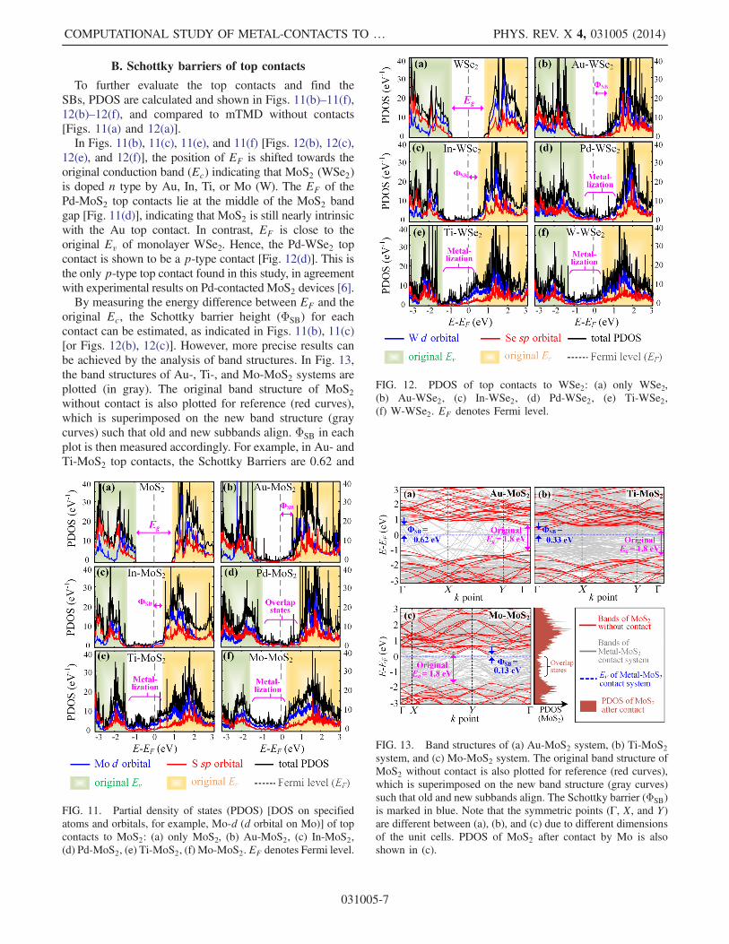
B. Schottky barriers of top contacts
To further evaluate the top contacts and find theSBs, PDOS are calculated and shown in Figs. 11(b)–11(f),12(b)–12(f), and compared to mTMD without contacts[Figs. 11(a) and 12(a)].In Figs. 11(b), 11(c), 11(e), and 11(f) [Figs. 12(b), 12(c),
12(e), and 12(f)], the position of EF is shifted towards theoriginal conduction band (Ec) indicating that MoS2 (WSe2)is doped n type by Au, In, Ti, or Mo (W). The EF of thePd-MoS2 top contacts lie at the middle of the MoS2 bandgap [Fig. 11(d)], indicating that MoS2 is still nearly intrinsicwith the Au top contact. In contrast, EF is close to theoriginal Ev of monolayer WSe2. Hence, the Pd-WSe2 topcontact is shown to be a p-type contact [Fig. 12(d)]. This isthe only p-type top contact found in this study, in agreementwith experimental results on Pd-contacted MoS2 devices [6].By measuring the energy difference between EF and the
original Ec, the Schottky barrier height (ΦSB) for eachcontact can be estimated, as indicated in Figs. 11(b), 11(c)[or Figs. 12(b), 12(c)]. However, more precise results canbe achieved by the analysis of band structures. In Fig. 13,the band structures of Au-, Ti-, and Mo-MoS2 systems areplotted (in gray). The original band structure of MoS2without contact is also plotted for reference (red curves),which is superimposed on the new band structure (graycurves) such that old and new subbands align. ΦSB in eachplot is then measured accordingly. For example, in Au- andTi-MoS2 top contacts, the Schottky Barriers are 0.62 and
FIG. 11. Partial density of states (PDOS) [DOS on specifiedatoms and orbitals, for example, Mo-d (d orbital on Mo)] of topcontacts to MoS2: (a) only MoS2, (b) Au-MoS2, (c) In-MoS2,(d) Pd-MoS2, (e) Ti-MoS2, (f) Mo-MoS2. EF denotes Fermi level.
FIG. 12. PDOS of top contacts to WSe2: (a) only WSe2,(b) Au-WSe2, (c) In-WSe2, (d) Pd-WSe2, (e) Ti-WSe2,(f) W-WSe2. EF denotes Fermi level.
FIG. 13. Band structures of (a) Au-MoS2 system, (b) Ti-MoS2system, and (c) Mo-MoS2 system. The original band structure ofMoS2 without contact is also plotted for reference (red curves),which is superimposed on the new band structure (gray curves)such that old and new subbands align. The Schottky barrier (ΦSB)is marked in blue. Note that the symmetric points (Γ, X, and Y)are different between (a), (b), and (c) due to different dimensionsof the unit cells. PDOS of MoS2 after contact by Mo is alsoshown in (c).
COMPUTATIONAL STUDY OF METAL-CONTACTS TO … PHYS. REV. X 4, 031005 (2014)
031005-7

0.33 eV, respectively, from DFT simulation as shown inFigs. 13(a) and 13(b). Using this approach, ΦSB for all ofthe top contacts is calculated and listed in Fig. 14.According to our recent experimental work (under review),the extracted Schottky barrier between Ti and monolayerMoS2 varies between 0.3 and 0.35 eV measured from 6monolayer devices, which is in agreement with the sim-ulation results (0.33 eV).Moreover, despite the high WF (4.5 eV) of Mo
[Fig. 2 (a)], the Fermi level is pinned at only 0.13 eV belowthe original Ec of intrinsic monolayer MoS2 [Fig. 2(c)],indicating a Schottky barrier of 0.13 eV at interface D inFig. 7(d). This Schottky barrier height is much lower thanthat of the Ti-MoS2 top contact [0.33 eV, as shown inFig. 13(b)], although Ti has a smaller WF that is also closerto the electron affinity of MoS2 [4.3 eV, Fig. 2(a)]. This alsoindicates that the properties of contacts to 2D materialscannot be intuitively predicted by WF values.It is instructive to note that such an abnormal Fermi level
pinning at the Mo-MoS2 interface is not caused by interfacetraps, which may consume incoming carriers, because ofthe absence of dangling bonds (interface traps) in MoS2.Since the MoS2 is monolayer, its properties can be easilydistorted by the strong orbital overlaps (covalent bonds),which create overlap states. Thus, the electronic propertiesof the MoS2 under the contact change. In other words, thecompound (Mo-MoS2 alloy) at the interface can beexpected to be a new material, which has a much lowerWF compared to that of the unalloyed MoS2 in the channelregion [Fig. 7(a)]. Hence, the unalloyed MoS2 (near thecontacts) is n-type doped as if it is contacted to a low-WFmetal. This phenomenon has also been confirmed in thesimulation of the Mo contact on multilayer MoS2 [38].On the other hand, it is also important to note that the
study of the unusual Fermi level pinning at the metal-TMDinterface requires careful treatment of the vdW interactionbetween them, which is usually missing in studies of 2Dinterfaces. Using pure LDA, no reliable predictions can bemade due to its limitations in handling vdW interactions[28]. In particular, LDA does not correctly reproduce theinterlayer binding energies [29]. DFT-D functionals givethe closest interlayer binding energy results for layered
MoS2 and WSe2 with respect to the comprehensively andexperimentally tested random-phase approximationmethod, compared with LDA, PBE GGA, and vdW-DF[28]. Also, considering its lower computational demands,DFT-D is more useful for describing vdW interaction.Hence, the adoption of the DFT-D2 (newer version ofDFT-D) functional in this work is highly necessary andsuitable, and thus the results are more reliable.
C. Orbital overlap of top contacts
Because of the lack of orbital overlaps, Au- andIn-mTMD top contacts are typical Schottky contacts [type1 in Fig. 7(b)]. In contrast, for Pd-MoS2 top contacts[Fig. 11(d)], overlap states can be found in the originalband gap of MoS2. This indicates that the Pd-MoS2 topcontact is type 2 [Fig. 7(c)]. As illustrated in Fig. 7(c), theseoverlap states contribute to the electron or hole injectionfrom the metal.As shown earlier, the overlap of Ti and S atomic spheres
can be clearly observed from the optimized geometry of theTi-MoS2 top contact Fig. 8(d), which indicates the highpossibility of covalent bond formation between Ti andMoS2. This is proved by Fig. 11(e), where the high PDOSspreads all over the original band gap, which represents theoverlap states corresponding to the covalent bonds. Hence,Ti-MoS2 has an Ohmic interface [at B in Fig. 7(d)], wherethe band gap vanishes and the MoS2 region under thecontact metal [Fig. 7(a)] is metallized. Similar results arealso found in Mo-MoS2, Ti-WSe2, Pd-WSe2, and W-WSe2top contacts. Hence, although Mo and W do not havesuitable WFs for MoS2 and WSe2, respectively, bothMo-MoS2 andW-WSe2 top contacts have Ohmic interfaces[B in Fig. 7(d)]. These results can be found only by atomiclevel modeling (i.e., DFT) and cannot be inferred intui-tively from analytical Schottky barrier theory.As shown in Figs. 13(b) and 13(c), most of the original
MoS2 bands (red) are disturbed by Ti orMo contact, formingnew bands (gray) that extend into the original band gap,which correspond to the covalent bands with overlap states,while most of the MoS2 bands in the Au-MoS2 systemremain the same as in pure MoS2 [Fig. 13(a)], indicating thelack of orbital overlaps. It is important to note that electronson the overlap states in the Ti- andMo-MoS2 systems are notlocalized, so that the metal will not degrade the conductivityof MoS2 under the contact. This can be confirmed by theshapes of the energy bands of the Ti- andMo-MoS2 system(gray curves) in Figs. 13(b) and 13(c), where most of theenergy bands have high enough curvature (indicating smalleffective mass) for efficient carrier transport.Valence electron densities of top contacts are calculated
and shown in Fig. 15. The minimum values of the x-y planeaverages (ρm) at the interfaces are measured and marked onthe curves or contours. The Au and In contacts give relativelylower ρm, indicating weak adhesion and, thus, weak orbitaloverlaps. For Pd top contacts, the corresponding values are
FIG. 14. ΦSB of all of the (a) MoS2 top contacts and (b) WSe2top contacts. ΦSB;N (ΦSB;P) denotes n type (p type) SB forelectrons (holes).
KANG et al. PHYS. REV. X 4, 031005 (2014)
031005-8

better (greater than 0.02 bohr−3), due to stronger overlap.Ti-mTMD contacts have high ρm values of 0.033 and0.029 bohr−3, implying that Ti has the possibility to achievestrong orbital overlaps with monolayer MoS2 and WSe2,leading to low contact resistance. Moreover, Mo-MoS2 andW-WSe2 have evenhigherρm at the interfaces than theothers,so that theMo andW top contacts can be expected to have thehighest electron injection efficiency among all of the topcontact metals.These predictions can also be confirmed by Mulliken
population analysis. The maximum bond Mulliken pop-ulations calculated from all of the top-contact interfaces arelisted and sorted in Fig. 16(a), compared with values inside
intrinsic MoS2 and WSe2. These two sequences of pop-ulations indicate the sequences of covalent bond strength.According to Fig. 16(a), the populations of Ti-S, Mo-S, andW-Se bonds at the interfaces (0.59, 0.67, 0.51) can be evenhigher than that of Mo-S (W-Se) bonds inside MoS2(WSe2) [0.53 (0.50)], which implies that stronger covalentbonds are formed at the interfaces than in mTMDs.Particularly, to prove the strong orbital overlaps ofTi-MoS2 top contacts, the bond Mulliken populations ofall Ti-S bonds at the Ti-MoS2 top contact interface areshown in Fig. 16(b), which range from 0.42 to 0.59 and aremuch higher than that for In, Au, and Pd.
D. Summary of top contacts
Based on the above analysis on tunnel barrier, Schottkybarrier, and orbital overlap, all of the top contacts can becategorized as follows, as summarized in Fig. 17.1. Au and In contacts are type 1. Between these two
metals, Au is favored for its better orbital overlap on MoS2[4] than that of In, while In is better in terms of Schottkybarrier height and more applicable to WSe2 [7].2. Although Pd is a type 2 metal on MoS2, the Schottky
barriers from Pd to MoS2 are relatively higher (0.90 eV forboth n- and p-type SB). Hence, Pd is not suitable for MoS2.However, compared to the Pd-MoS2 contact, Pd-WSe2provides a much lower p-type Schottky barrier (0.35 eV)and much higher overlap states or metallization, whichmakes Pd-WSe2 to be beyond type 2 and is somewherebetween type 2 and type 3.3. Ti-MoS2 top contact can be expected to have excellent
electron injection efficiency. It can be categorized as type 3due to the strong metallization and absence of TB at theinterface. Ti also provides strong metallization toWSe2, butan unexpected tunnel barrier degrades its performance oncontacting WSe2. Hence, the Ti-WSe2 top contact is ratedbetween type 2 and type 3.4. Based on DFT simulations presented above, Mo
shows great potential as a high-quality contact metal forMoS2 and is classified as type 3. Mo is superior in terms ofSchottky barrier (0.13 eV) than that of Ti-MoS2 top contact(0.33 eV). However, the PDOS near the Fermi level ofMoS2 under the Mo contact [marked by the purple brace inFig. 11(f)] is slightly lower than that of MoS2 under the Ticontact [Fig. 11(e)], which may counter Mo’s advantage oflower Schottky barrier compared to that in the case of Ti.This is in agreement with our recent measurements onMo-MoS2 contacts [38], where Mo and Ti contacts exhibitvery similar contact resistances.5. Similar to Mo-MoS2, W-WSe2 is also an excellent
type 3 contact. Despite its high WF, W provides n-typecontact on WSe2 due to Fermi level pinning since it formsan alloy whose WF is close to the electron affinity of WSe2.
E. Exploration of edge contacts
Edge contacts become more important when the top-contact area is limited or in multilayered structures
FIG. 15. Valence electron densities (bohr−3) ofmetal-mTMD topcontacts: (a) Au-MoS2, (b) In-MoS2, (c) Mo-MoS2, (d) Pd-MoS2,(e) Ti-MoS2, (f) Au-WSe2, (g) In-WSe2, (h) Pd-WSe2, (i) Ti-WSe2,(j)W-WSe2. Panel (c) and the left-hand contours in (a) and (b) showaveragedensity alongxprojectedon they-zplane.Panels (d)–(j) andthe right-hand plots in (a) and (b) show average electron densityvalue in the x-y planes normal to the z axis (ρe). ρm in each panelindicates the minimum x-y plane average electron density at eachinterface (in units of bohr−3).
FIG. 16. (a) Maximum bond Mulliken populations (on a scaleof 0 to 1) of top-contact interface bonds (colored numbers)compared to that of Mo-S (W-Se) bonds inside mTMDs (blacknumbers). (b) Bond Mulliken populations of the Ti-MoS2 topcontact. Population values are marked beside each interface bond.Population values of Mo-S bonds are also marked in MoS2.
COMPUTATIONAL STUDY OF METAL-CONTACTS TO … PHYS. REV. X 4, 031005 (2014)
031005-9

[12,39,40]. In real situations, edge contacts can be inducedby proper layout design. Moreover, edge contacts can bemore significant for metal contacts to multilayer TMDs thanthat to mTMDs because more edges can be contacted tometals.In this work, Au, In, Pd, and Ti are chosen for modeling
edge-contact configurations. In all of the simulatedmetal-mTMD edge contacts, the physical separations (d)are much smaller (Table I) than that of top contacts[Fig. 10(b)], because of the formation of covalent bondsbetween the metal and mTMD as shown in Fig. 18, whereoverlaps of metal and chalcogenide atomic spheres can befound in each of the edge contacts. Hence, tunnel barrierwidths are reduced using edge-contact configuration andedge contacts have a high possibility of covalent bondformation between metals and mTMDs.As shown in Fig. 19, Veff’s along the z axis are smoother
at the interfaces with smaller tunnel barriers (Table I)compared to those for top contacts. For example, theAu-MoS2 top contact has an effective tunnel barrier heightof 0.67 Ry [Fig. 10(a)], while the height in the Au-MoS2edge contact is reduced to 0.54 Ry [Fig. 19(a)], which allowshigher electron injection efficiency than that of top contacts.Moreover, in the In-MoS2 edge contact, the ΦTB;eff vanishes[Fig. 19(b)], compared to that of the top contact. Thisphenomenon is also found in Pd edge contacts.PDOS of edge contacts are shown in Fig. 20. SBs and
band gaps are absent in all of the edge contacts. Themetallization is mainly due to stronger orbital overlaps,which induce high density of states in the original band gaps.
Minimum valence electron densities at the interfaces(ρmin) are increased compared to that of most of the topcontacts, as shown in Figs. 21(a) and 21(b), due to thestrong orbit overlap (covalent bonds) between metal andmTMD atoms. In particular, ρmin in Au-MoS2 [Figs. 21(c)and 21(d)] and In-mTMD edge contacts are significantlyincreased compared to that of their top contacts[Figs. 15(a), 15(b), and 15(g)], indicating a decrease inresistance by changing contact configurations from topcontacts into combined contacts [Fig. 3(c)]. Low contactresistance of combined-contact configuration has beendemonstrated on Au-MoS2 [4], Ti-MoS2 [12] andIn-WSe2 [7] contacts via experiments.Furthermore, the electron localization functions (ELF, a
function of the 3D coordinates, which is large in the regionswhere orbitals localize [41]) for Au-MoS2 top and edgecontacts [Figs. 22(a) and 22(c)] are calculated and shown inFigs. 22(b) and 22(d). Because orbital overlaps betweenmetal and mTMD atoms are more efficient in edge contacts,the ELF at the metal-mTMD interface is much higher at the
TABLE I. Evaluation of tunnel barriers at metal-mTMDedge-contact interfaces.
MoS2 WSe2In Ti Au Pd In Ti Au Pd
d (Å) 1.38 0.84 1.70 1.72 1.54 1.32 2.18 1.89ΦTB;eff (Ry) 0.00 0.00 0.54 0.12 0.00 0.00 0.12 0.00
FIG. 17. Summary of metal-mTMD top-contact electron in-jection efficiency, in terms of orbital overlap, Schottky barrier,and tunnel barrier.
FIG. 18. Optimized geometries of edge contacts: (a) Au-MoS2(in different views), (b) In-MoS2, (c) Pd-MoS2, (d) Ti-MoS2,(e) Au-WSe2 (in different views), (f) In-WSe2, (g) Pd-WSe2, and(h) Ti-WSe2. The large-volume overlaps of metal and chalco-genide atomic spheres exist in every edge contact [in (a)–(h)],indicating the formation of strong covalent bonds. Hence,physical separations in edge contacts (Table I) are much smallerthan that of top contacts in Figs. 8 and 9 due to the covalent bondsformed between mTMD and metals.
KANG et al. PHYS. REV. X 4, 031005 (2014)
031005-10

interface in edge contacts [Fig. 22(d)] than that of topcontacts [Fig. 22(b)]. In other words, strong covalent bondsare formed in edge contacts, indicated by green dashedcurves in Fig. 22(d).The strong orbital overlaps, absence of SB, and lower
tunnel barriers are all advantages of edge-contact configu-rations compared to top contacts. Hence, edge-contactedconfigurations have a higher capability of electron injectionand thereby decrease the contact resistance. If contactdimensions are large (i.e., number of atoms across the
contact area is much greater than those along the contactperimeter), top contacts have an advantage in terms ofcontact area. However, for a fixed number of mTMD atomscontacted by metal, the edge-contacted configuration isbetter than the top-contacted configuration. Hence, thecombined contact [Fig. 3(c), combination of top contactand edge contact] is more desirable. It is worth noting thatfor multilayer TMD devices, due to process voids, theelectrode metal may fail to contact all of the layers at theedges, and the gate electrode may not modulate allthe layers due to screening. Therefore, the number ofTMD layers should be optimized [12].
FIG. 19. Minimum Veff of (a) Au-MoS2 edge contact and(b) In-MoS2 edge contact. ΦMoS2 is the Veff of the Mo-S bondorbitals and thereby the effective tunnel barrier height (ΦTB;eff ) isdefined as the minimum barrier height that an electron from themetal has to overcome, if it has the same potential energy asΦMoS2 . Hence, ΦTB;eff can be calculated as the Veff differencebetween the vdW gap (Φgap) and MoS2 (ΦMoS2 ). Φmetal;mindenotes the minimum Veff that an electron can have in the metal.It is worth noting that in some metals [such as in (a)]Φmetal;min canbe higher than ΦMoS2 (thus, electron energy is always higher thanthat of Mo-S bond orbitals), in which case ΦTB;eff is calculated asΦTB;eff ¼ Φgap − Φmetal;min. d is defined as the physical separation(the z component of the nearest core-to-core distance between themetal atoms and the chalcogenide atoms). Though d does notvanish, ΦTB;eff can vanish, when Φmetal;min or ΦMoS2 is higher thanΦgap, such as in (b).
FIG. 20. PDOS of mTMD near EF of edge contacts to (a)–(d) MoS2 and (e)–(h) WSe2. Because of orbital overlaps (covalentbonds) at the interfaces, all the mTMDs in edge contacts haveoverlap states in the original band gaps and near EF, so thatmTMDs are metallized by edge contacts.
FIG. 21. (a),(b) Minimum of average electron density values inthe x-y plane in Fig. 18(a) at the interfaces for all top and edgecontacts. Ti, Pd, Mo, and W may form better top contacts due tohigher interface electron density. Electron densities are signifi-cantly increased for edge contacts. (c),(d) Valence electrondensities of Au-MoS2 edge contact. (c) Average density alongy projected on the x-z plane; (d) average density in the x-y planesnormal to the z axis. The red number in (d) indicates theminimum electron density at the interface.
FIG. 22. (a),(c) The cleaved x-z planes (red rectangles) used toshow electron localization functions (ELF) for (a) Au-MoS2 topcontact and (c) Au-MoS2 edge contact. (b),(d) ELF plots on thecleaved x-z plane in Au-MoS2 (b) top contact, (d) edge contact.Half-transparent dots indicate positions of atoms. High ELF(closer to 1) indicates high probability of finding an electron. Foredge contact, Au-MoS2 has overlapping electron orbitals (Au-Sbonds, indicated by green dashes) resulting in the increasing ofelectron density as shown in Fig. 21. Thus, the contact resistanceis reduced by using edge contacts.
COMPUTATIONAL STUDY OF METAL-CONTACTS TO … PHYS. REV. X 4, 031005 (2014)
031005-11

IV. SUMMARY
This work presented a systematic and rigorous study ofthe physical nature of metal-mTMD interfaces. The elec-tron injection efficiency of the interfaces is shown to becharacterized by three key criteria—tunnel barrier,Schottky barrier, and orbital overlap. In order to accuratelycapture each of those criteria, DFT simulations incorpo-rating semiempirical vdW potential are employed for thefirst time for metal-mTMD interfaces, and optimizedgeometries, effective potential, band structures, PDOS,valence electron densities, and bond Mulliken populationsof metal-mTMD contacts are calculated.We find that Ti and Mo are the best top-contact metals for
monolayer intrinsic MoS2 and are n-type contact metals(Fig. 17). Pd is the best p-type top-contact metal formonolayer intrinsic WSe2 (Fig. 17) while W can achievehigh-quality n-type top contacts with WSe2 due to the strongorbital overlaps and vanishing of Schottky barriers (Fig. 17).These findings are summarized and shown in Fig. 17.While none of the metals studied in this work indicate the
capability of forming good p-type contacts to MoS2, fromthe basic interface physics revealed in this study, materialswith strong orbital overlaps with MoS2 have the potential tolead to such contacts. Such properties can possibly be foundin molybdenum oxide compounds (MoOx).It is also shown that edge-contacted configurations can
improve the contact by lowering tunnel barriers andstrengthening the orbital overlaps. With the right metaland certain contact area, in order to achieve the lowestcontact resistance, it is desirable to combine edge contactwith top contact for monolayer TMDs [Fig. 3(c)]. It can beinferred that inducing of edge contacts can be moresignificant for multilayer mTMDs. For more-than-ten-layerTMDs, it is necessary to ensure that all of the edges arecontacted to the metal using the tilt deposition technique[42]. On the other hand, it is possible to increase the edge-contact length for lower contact resistance, for example, bycutting mTMD edges into jagged edges.The results obtained in this study not only reveal the
types of metals and configurations that can be employed forachieving low contact resistance with MoS2 and WSe2, butalso highlight that the properties of contacts cannot beintuitively predicted by solely considering WF values (e.g.,Au versus Pd; In versus Ti; Mo or W versus other metals).Moreover, the significance of the developed framework,which features vdW interactions and bond Mulliken pop-ulation analysis is apparent not only for contacts to various2D materials, but also for understanding the nature ofinterfaces to a wide variety of 2D materials, which will be akey issue in optimizing the performance of all emerging 2Dmaterials-based devices including the recently proposedconcept of “all-2D devices and circuits” [43] (wheregraphene is used as gate electrodes and interconnects,MoS2 andWSe2 are used as channel materials in the FETs,and insulating h-BN is used as a gate dielectric). By
combining our framework and transport simulations, quan-titative values of contact resistances can be calculated in thefuture.
ACKNOWLEDGMENTS
This work was supported by the National ScienceFoundation (Grant No. CCF-1162633).
APPENDIX: BAND STRUCTURE EVALUATIONFOR DFT-D2 WITH LDA
As pointed out in Section II C, the DFT-D2 results showconsistent bandgaps with results from experiments [25,26].Since the valence band structures of bulk MoS2 wererecently measured by angle-resolved photoemission spec-troscopy (ARPES) as reported in [44], to further evaluate thesimulation methodology, the calculated valence band struc-tures of bulk MoS2 by DFT-D2 with LDA (black curves) aresuperimposed on that of ARPES results (red dots) from [44],as shown in Fig. 23. It can be observed that the shapes ofelectronic dispersion spectrum of MoS2 in simulations are inagreement with those from the experiments.This provides strong evidence that the methodology
employed in this work can reproduce the electronicspectrum correctly and the agreements between simulationsand experiments are not just coincidental.
[1] K. S. Novoselov, A. K. Geim, S. V. Morozov, D. Jiang, Y.Zhang, S. V. Dubonos, I. V. Grigorieva, and A. A. Firsov,Electric Field Effect in Atomically Thin Carbon Films,Science 306, 666 (2004).
[2] A. K. Geim and K. S. Novoselov, The Rise of Graphene,Nat. Mater. 6, 183 (2007).
FIG. 23. Comparison of calculated (DFT-D2 with LDA) andexperimentally measured (ARPES) [44] valence band structuresof MoS2. The valence band maxima is set to zero energy.
KANG et al. PHYS. REV. X 4, 031005 (2014)
031005-12

[3] G.-H. Lee, Y.-J. Yu, C. Lee, C. Dean, K. L. Shepard, P. Kim,and J. Hone, Electron Tunneling through Atomically Flatand Ultrathin Hexagonal Boron Nitride, Appl. Phys. Lett.99, 243114 (2011).
[4] B. Radisavljevic, A. Radenovic, J. Brivio, V. Giacometti,and A. Kis, Single-Layer MoS2 Transistors, Nat.Nanotechnol. 6, 147 (2011).
[5] Y. Yoon, K. Ganapathi, and S. Salahuddin, How Good CanMonolayer MoS2 Transistors Be?, Nano Lett. 11, 3768(2011).
[6] H. Fang, S. Chuang, T. C. Chang, and K. Takei,High-Performance Single Layered WSe2 P-FETs withChemically Doped Contacts, Nano Lett. 12, 3788 (2012).
[7] W. Liu, J. Kang, D. Sarkar, Y. Khatami, D. Jena, and K.Banerjee, Role of Metal Contacts in Designing High-Performance Monolayer n-Type WSe2 Field EffectTransistors, Nano Lett. 13, 1983 (2013).
[8] S. Kim, A. Konar, W. Hwang, J. H. Lee, J. Lee, J. Yang, C.Jung, H. Kim, J. Yoo, J. Choi, Y.W. Jin, S. Y. Lee, D. Jena,W. Choi, and K. Kim, High-Mobility and Low-Power Thin-Film Transistors based on Multilayer MoS2 Crystals, Nat.Commun. 3, 1011 (2012).
[9] D. Sarkar, W. Liu, X. Xie, A. Anselmo, S. Mitragotri,and K. Banerjee, MoS2 Field-Effect Transistor for Next-Generation Label-Free Biosensors, ACS Nano 8, 3992(2014).
[10] I. Popov, G. Seifert, and D. Tománek, Designing ElectricalContacts to MoS2 Monolayers: A Computational Study,Phys. Rev. Lett. 108, 156802 (2012).
[11] S. Das, H.-Y. Chen, A. V. Penumatcha, and J. Appenzeller,High Performance Multilayer MoS2 Transistors withScandium Contacts, Nano Lett. 13, 100 (2013).
[12] W. Liu, J. Kang, W. Cao, D. Sarkar, Y. Khatami, D. Jena,and K. Banerjee, in Proceedings of the IEEE InternationalElectron Devices Meeting, 2013 (IEEE, New York, 2013),pp. 499–502.
[13] L.-Y. Gan, Y.-J. Zhao, D. Huang, and U. Schwingenschlögl,First-Principles Analysis ofMoS2=Ti2C andMoS2=Ti2CY2
(Y ¼ F and OH) All-2D Semiconductor/Metal Contacts,Phys. Rev. B 87, 245307 (2013).
[14] International Technology Roadmap for Semiconductors,http://www.itrs.net/.
[15] H. Liu, A. T. Neal, and P. D. Ye, Channel Length Scaling ofMoS2 MOSFETs, ACS Nano 6, 8563 (2012).
[16] E. K. U. Gross and R. M. Dreizler, Density FunctionalTheory (Plenum, New York, 1993).
[17] J. Kang, D. Sarkar, W. Liu, D. Jena, and K. Banerjee, inProceedings of the IEEE International Electron DevicesMeeting, 2012 (IEEE, New York, 2012), pp. 407–410.
[18] Handbook of Chemistry and Physics, edited by V. R. C.Weast (CRC Press, Boca Raton, FL, 1979), 59th ed., p. 114.
[19] P. Bhattacharya, Semiconductor Optoelectronic Devices(Prentice-Hall, Englewood Cliffs, NJ, 1997), 2nd ed.
[20] Y. Li, Z. Zhou, S. Zhang, and Z. Chen, MoS2 Nanoribbons:High Stability and Unusual Electronic and MagneticProperties, J. Am. Chem. Soc. 130, 16 739 (2008).
[21] Y. Matsuda, W.-Q. Deng, and W. A. Goddard, ContactResistance for “End-Contacted” Metal-Graphene andMetal-Nanotube Interfaces from Quantum Mechanics, J.Phys. Chem. C 114, 17 845 (2010).
[22] W. Kohn and L. J. Sham, Self-Consistent Equations Includ-ing Exchange and Correlation Effects, Phys. Rev. 140,A1133 (1965).
[23] J. P. Perdew, K. Burke, and M. Ernzerhof, GeneralizedGradient Approximation Made Simple, Phys. Rev. Lett. 77,3865 (1996); 78, 1396(E) (1997).
[24] J. P. Perdew and A. Zunger, Self-Interaction Correction toDensity-Functional Approximations for Many-ElectronSystems, Phys. Rev. B 23, 5048 (1981).
[25] K. F. Mak, C. Lee, J. Hone, J. Shan, and T. F. Heinz,Atomically Thin MoS2: A New Direct-Gap Semiconductor,Phys. Rev. Lett. 105, 136805 (2010).
[26] D. Voβ, P. Krüger, A. Mazur, and J. Pollmann, Atomic andElectronic Structure of WSe2 from Ab Initio Theory: BulkCrystal and Thin Film Systems, Phys. Rev. B 60, 14 3111999).
[27] M. Vanin, J. J. Mortensen, A. K. Kelkkanen, J. M. Garcia-Lastra, K. S. Thygesen, and K.W. Jacobsen, Graphene onMetals: A van der Waals Density Functional Study, Phys.Rev. B 81, 081408 (2010).
[28] T. Björkman, A. Gulans, A. V. Krasheninnikov, and R. M.Nieminen, Are We van der Waals Ready?, J. Phys. Condens.Matter 24, 424218 (2012).
[29] T. Björkman, A. Gulans, A. V. Krasheninnikov, and R. M.Nieminen, van der Waals Bonding in Layered Compoundsfrom Advanced Density-Functional First-PrinciplesCalculations, Phys. Rev. Lett. 108, 235502 (2012).
[30] S. Grimme, Accurate Description of van der WaalsComplexes by Density Functional Theory IncludingEmpirical Corrections, J. Comput. Chem. 25, 1463 (2004).
[31] S. Grimme, Semiempirical GGA-Type Density FunctionalConstructed with a Long-Range Dispersion Correction, J.Comput. Chem. 27, 1787 (2006).
[32] S. Grimme, J. Antony, S. Ehrlich, and H. Krieg, A Con-sistent and Accurate Ab Initio Parametrization of DensityFunctional Dispersion Correction (DFT-D) for the 94Elements H-Pu, J. Chem. Phys. 132, 154104 (2010).
[33] Y. Andersson, D. C. Langreth, and B. I. Lundqvist, van derWaals Interactions in Density-Functional Theory, Phys.Rev. Lett. 76, 102 (1996).
[34] D. C. Langreth, M. Dion, H. Rydberg, E. Schröder,P. Hyldgaard, and B. I. Lundqvist, van der Waals DensityFunctional Theory with Applications, Int. J. QuantumChem. 101, 599 (2005).
[35] T. Sato, T. Tsuneda, and K. Hirao, van der Waals Inter-actions Studied by Density Functional Theory, Mol. Phys.103, 1151 (2005).
[36] Atomistix ToolKit v.13.8.0, QuantumWise A/S, http://www.quantumwise.com/
[37] R. S. Mulliken, Electronic Population Analysis on LCAO-MO Molecular Wave Functions. I, J. Chem. Phys. 23, 1833(1955).
[38] J. Kang, W. Liu, and K. Banerjee, High-PerformanceMoS2Transistors with Low-Resistance Molybdenum Contacts,Appl. Phys. Lett. 104, 093106 (2014).
[39] Y. Khatami, H. Li, C. Xu, and K. Banerjee, Metal-to-Multilayer-Graphene Contact—Part I: Contact ResistanceModeling, IEEE Trans. Electron Devices 59, 2444 (2012).
[40] Y. Khatami, H. Li, C. Xu, and K. Banerjee, Metal-to-Multilayer-Graphene Contact—Part II: Analysis of Contact
COMPUTATIONAL STUDY OF METAL-CONTACTS TO … PHYS. REV. X 4, 031005 (2014)
031005-13

Resistance, IEEE Trans. Electron Devices 59, 2453(2012).
[41] A. D. Becke and K. E. Edgecombe, A Simple Measure ofElectron Localization in Atomic and Molecular Systems,J. Chem. Phys. 92, 5397 (1990).
[42] H. Li, W. Liu, A. M. Cassell, F. Kreupl, and K. Banerjee,Low-Resistivity Long-Length Horizontal Carbon NanotubeBundles for Interconnect Applications—Part I: ProcessDevelopment, IEEE Trans. Electron Devices 60, 2862(2013).
[43] W. Cao, J. Kang, W. Liu, Y. Khatami, D. Sarkar, andK. Banerjee, in Proceedings of the 43rd EuropeanSolid-State Device Research Conference (ESSDERC),Bucharest, Romania, 2013 (IEEE, New York, 2013),pp. 37–44.
[44] S. K. Mahatha, K. D. Patel, and K. S. R. Menon, ElectronicStructure Investigation of MoS2 and MoSe2 Using Angle-Resolved Photoemission Spectroscopy and Ab Initio BandStructure Studies, J. Phys. Condens. Matter 24, 475504(2012).
KANG et al. PHYS. REV. X 4, 031005 (2014)
031005-14


![Interactions between Phospholipid Monolayers (DPPC and DMPC) … · 2015. 6. 10. · processes occurring on a self-assembled monolayer [18], metal ion binding to the Langmuir monolayer](https://img.pdfslide.net/doc/110x75/600d3401e529355e3642b483/interactions-between-phospholipid-monolayers-dppc-and-dmpc-2015-6-10-processes.jpg)