Embed Size (px)
Citation preview
Victor P. Nelson VLSI Design & Test Seminar
11/05/2011
Computer-Aided Design of ASICs Concept to Silicon
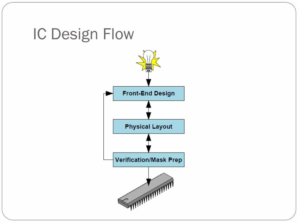
IC Design Flow
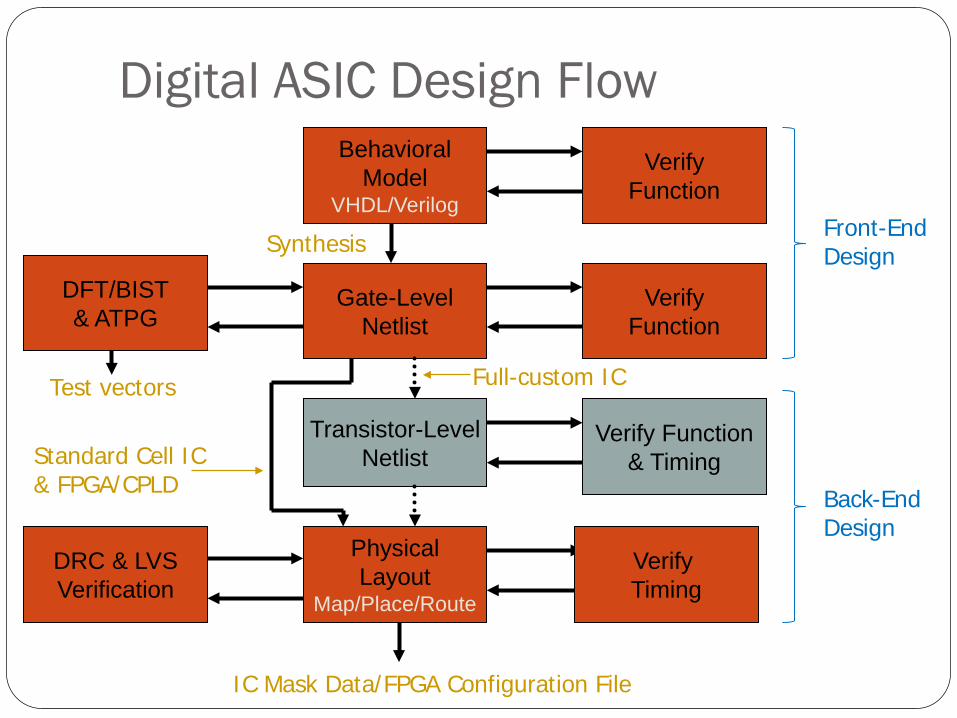
Digital ASIC Design Flow Behavioral
Model VHDL/Verilog
Gate-Level Netlist
Transistor-Level Netlist
Physical Layout
Map/Place/Route
DFT/BIST & ATPG
Verify Function
Verify Function
Verify Function & Timing
Verify Timing
DRC & LVS Verification
IC Mask Data/FPGA Configuration File
Standard Cell IC & FPGA/CPLD
Synthesis
Test vectors Full-custom IC
Front-End Design
Back-End Design
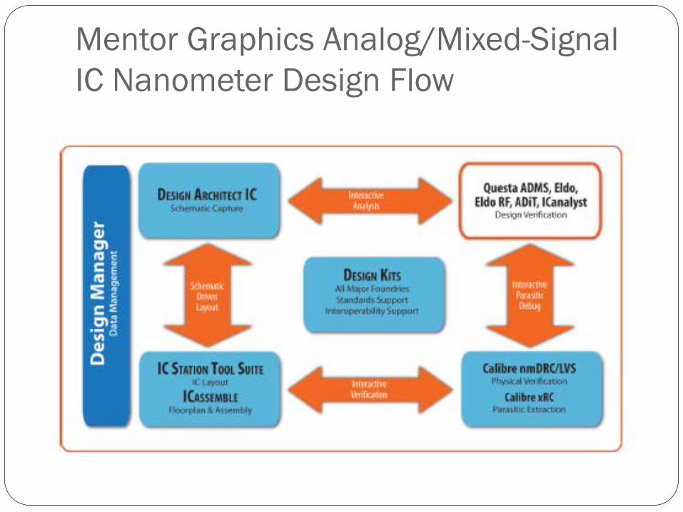
Mentor Graphics Analog/Mixed-Signal IC Nanometer Design Flow

ASIC CAD tools available in ECE Modeling and Simulation
Questa ADMS = Questa+Modelsim+Eldo+ADiT (Mentor Graphics) Verilog-XL, NC_Verilog, Spectre (Cadence)
Design Synthesis (digital) Leonardo Spectrum (Mentor Graphics) Design Compiler (Synopsys), RTL Compiler (Cadence)
Design for Test and Automatic Test Pattern Generation Tessent DFT Advisor, Fastscan, SoCScan (Mentor Graphics)
Schematic Capture & Design Integration Design Architect-IC (Mentor Graphics) Design Framework II (DFII) - Composer (Cadence)
Physical Layout IC Station (Mentor Graphics) SOC Encounter, Virtuoso (Cadence)
Design Verification Calibre DRC, LVS, PEX (Mentor Graphics) Diva, Assura (Cadence)

Mentor Graphics ASIC Design Kit (ADK)
Technology files & standard cell libraries AMI: ami12, ami05 (1.2, 0.5 μm) TSMC: tsmc035, tsmc025, tsmc018 (0.35, 0.25**, 0.18 μm) **also have VT Cadence lib Current MOSIS Instructional: IBM 180nm CMOS (7RF), ON Semi 0.5um CMOS Current MOSIS Unfunded Research: IBM 130nm CMOS (8RF), 130nm SiGE BiCMOS(8HP)
IC flow & DFT tool support files: Simulation models
VHDL/Verilog/Mixed-Signal models (Modelsim SE/Questa ADMS) Analog (SPICE) models (Eldo, ADiT) *Post-layout timing (Mach TA) * obsolete: Mach TA replaced by ADiT *Digital schematic (Quicksim II, Quicksim Pro) * obsolete: HDL or Eldo now used
Standard cell synthesis libraries (LeonardoSpectrum) Design for test & ATPG libraries (DFT Advisor, Fastscan) Schematic capture (Design Architect-IC) IC physical design (standard cell & custom)
Standard cell models, symbols, layouts (IC Station) Design rule check, layout vs schematic, parameter extraction (Calibre)
We also have ADK’s for Cadence tools for several technologies

Xilinx/Altera FPGA/CPLD Design Tools Simulate designs in Modelsim
Behavioral models (VHDL,Verilog) Synthesized netlists (VHDL, Verilog)
Requires “primitives” library for the target technology
Synthesize netlist from behavioral model Leonardo (Levels 1,2,3) has libraries for most FPGAs (ASIC-only license currently installed) Xilinx ISE and Altera Quartus II have own synthesis tools
Vendor tools for back-end design Map, place, route, configure device, timing analysis, generate timing models Xilinx Integrated Software Environment (ISE) Altera Quartus II & Max+Plus2
Higher level tools for system design & management Mentor Graphics FPGA Advantage Xilinx Platform Studio : SoC design, IP management, HW/SW codesign

Automated ASIC Design Flow Source: CMOS IC Layout, Dan Clein
Std Cell ASIC Full Custom IC
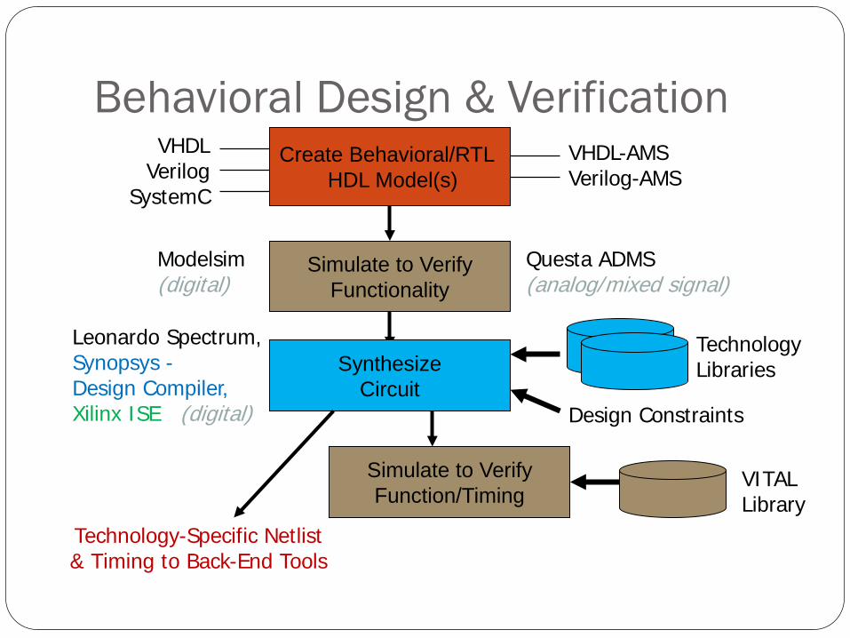
Behavioral Design & Verification Create Behavioral/RTL
HDL Model(s)
Simulate to Verify Functionality
Synthesize Circuit
Leonardo Spectrum, Synopsys - Design Compiler, Xilinx ISE (digital)
Modelsim (digital)
VHDL-AMS Verilog-AMS
Questa ADMS (analog/mixed signal)
VHDL Verilog
SystemC
Technology Libraries
Technology-Specific Netlist & Timing to Back-End Tools
Simulate to Verify Function/Timing
VITAL Library
Design Constraints

Questa ADMS (replaced ADVance MS)
Four simulation engines integrated for SoC designs Questa – mixed signal simulation (VHDL-AMS, Verilog-AMS) QuestaSim (Modelsim) – VHDL/Verilog/SystemC digital simulation Eldo/Eldo RF – analog (SPICE) simulation (replaced Accusim) ADiT – accelerated transistor-level (Fast-SPICE) simulation (replaced Mach TA)
Engines, languages, standards can be mixed in a simulation IEEE 1497 Standard Delay File Format (SDF) IEEE 1076.1 VHDL-AMS IEEE 1076 VHDL IEEE 1364 Verilog IEEE 1800 SystemVerilog IEEE 1666 SystemC Accellera standard Verilog-AMS Language SPICE Eldo, HSPICE, and Spectre dialects.
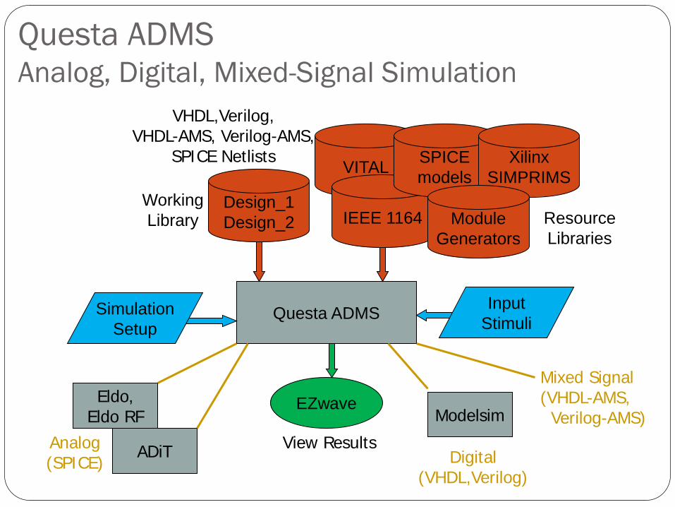
Questa ADMS Analog, Digital, Mixed-Signal Simulation
Questa ADMS
Working Library
Design_1 Design_2
VITAL
IEEE 1164 Resource Libraries
Simulation Setup
EZwave
Input Stimuli
VHDL,Verilog, VHDL-AMS, Verilog-AMS,
SPICE Netlists
Eldo, Eldo RF Modelsim
View Results ADiT Analog (SPICE) Digital
(VHDL,Verilog)
Mixed Signal (VHDL-AMS, Verilog-AMS)
SPICE models
Xilinx SIMPRIMS
Module Generators

Questa ADMS : mixed-signal simulation
A/D converter
digital analog VHDL-AMS
digital nets analog nets

Questa ADMS: mixed Verilog-SPICE
SPICE subcircuit
Verilog top (test bench)
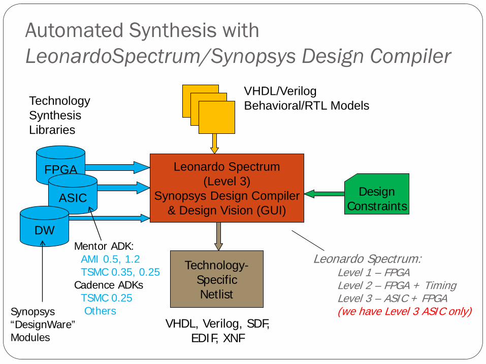
Automated Synthesis with LeonardoSpectrum/Synopsys Design Compiler
Leonardo Spectrum (Level 3)
Synopsys Design Compiler & Design Vision (GUI)
VHDL/Verilog Behavioral/RTL Models
FPGA
ASIC
Technology Synthesis Libraries
Technology- Specific Netlist
Design Constraints
VHDL, Verilog, SDF, EDIF, XNF
Leonardo Spectrum: Level 1 – FPGA Level 2 – FPGA + Timing Level 3 – ASIC + FPGA (we have Level 3 ASIC only)
Mentor ADK: AMI 0.5, 1.2 TSMC 0.35, 0.25 Cadence ADKs TSMC 0.25 Others
DW
Synopsys “DesignWare” Modules

Leonardo – ASIC Synthesis Flow
Read & check HDL
Synthesize generic gates & modules
Map to technology cells & optimize
Write netlist, SDF, reports

Sample LeonardoSpectrum synthesis script load_library /linux_apps/ADK3.1/technology/leonardo/tsmc025_typ analyze "../src/mux.vhd" "../src/shiftreg.vhd" "../src/alu.vhd"
"../src/dcontrol.vhd" "../src/divider.vhd“ elaborate clock_cycle 2 CLOCK optimize -hierarchy preserve optimize_timing -through C/reg_State(2)/Q write divider_0.vhd write divider_0.v write_divider_0.sdf report_area div_area.rpt -cell_usage –hierarchy report_delay div_delay.rpt report_delay -longest_path -to Q* mod6_outdelay.rpt report_delay -longest_path -from [list I* L_Cbar] mod6_indelay.rpt

Post-synthesis simulation of synthesized netlist
Verify that synthesized netlist matches behavioral model Create library of std cell simulation primitives: >vlib adk >vcom $ADK/technology/adk.vhd >vcom $ADK/technology/adk_comp.vhd
Insert library/package declaration into netlist library adk; use adk.adk_components.all; Simulate in Modelsim, using “do file” or test bench from
behavioral simulation results should match
Simulate netlist with synthesize-produced SDF file to study timing (delays, constraints, etc.)
VITAL models of ADK std cells

Post-synthesis timing analysis Synthesis tools generate SDF (std. delay format) file with technology-
specific, VITAL-compliant timing parameters (from cell library) (CELLTYPE "dffr") (INSTANCE Q_0_EXMPLR_EXMPLR) (DELAY (ABSOLUTE (PORT D (::0.00) (::0.00)) (PORT CLK (::0.00) (::0.00)) (PORT R (::0.00) (::0.00)) (IOPATH CLK Q (::0.40) (::0.47)) (IOPATH R Q (::0.00) (::0.55)) (IOPATH CLK QB (::0.45) (::0.36)) (IOPATH R QB (::0.53) (::0.00)))) (TIMINGCHECK (SETUP D (posedge CLK) (0.47)) (HOLD D (posedge CLK) (-0.06))))
Path delays (min:typ:max)
Delays lumped at pins
Clock constraints
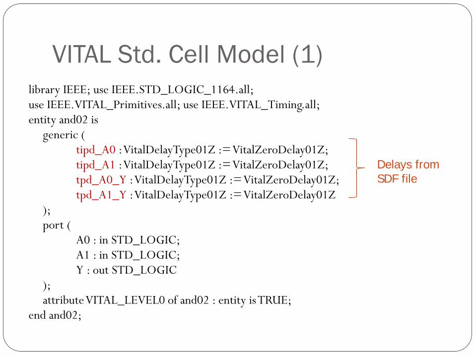
VITAL Std. Cell Model (1) library IEEE; use IEEE.STD_LOGIC_1164.all; use IEEE.VITAL_Primitives.all; use IEEE.VITAL_Timing.all; entity and02 is generic ( tipd_A0 : VitalDelayType01Z := VitalZeroDelay01Z; tipd_A1 : VitalDelayType01Z := VitalZeroDelay01Z; tpd_A0_Y : VitalDelayType01Z := VitalZeroDelay01Z; tpd_A1_Y : VitalDelayType01Z := VitalZeroDelay01Z ); port ( A0 : in STD_LOGIC; A1 : in STD_LOGIC; Y : out STD_LOGIC ); attribute VITAL_LEVEL0 of and02 : entity is TRUE; end and02;
Delays from SDF file
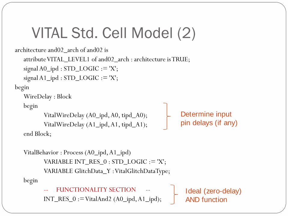
VITAL Std. Cell Model (2) architecture and02_arch of and02 is attribute VITAL_LEVEL1 of and02_arch : architecture is TRUE; signal A0_ipd : STD_LOGIC := 'X'; signal A1_ipd : STD_LOGIC := 'X'; begin WireDelay : Block begin VitalWireDelay (A0_ipd, A0, tipd_A0); VitalWireDelay (A1_ipd, A1, tipd_A1); end Block; VitalBehavior : Process (A0_ipd, A1_ipd) VARIABLE INT_RES_0 : STD_LOGIC := 'X'; VARIABLE GlitchData_Y : VitalGlitchDataType; begin -- FUNCTIONALITY SECTION -- INT_RES_0 := VitalAnd2 (A0_ipd, A1_ipd);
Determine input pin delays (if any)
Ideal (zero-delay) AND function

VITAL Std. Cell Model (3) -- PATH DELAY SECTION -- VitalPathDelay01Z ( -- VITAL Function Call OutSignal => Y, OutSignalName => "Y", OutTemp => INT_RES_0, Paths => ( 0 => ( InputChangeTime => A0_ipd'LAST_EVENT, PathDelay => tpd_A0_Y, PathCondition => TRUE ), 1 => ( InputChangeTime => A1_ipd'LAST_EVENT, PathDelay => tpd_A1_Y, PathCondition => TRUE ) ), GlitchData => GlitchData_Y, Mode => OnDetect, MsgOn => TRUE, Xon => TRUE, MsgSeverity => WARNING
Determine delay along each input-output path

Design for test & test generation Consider test during initial design phase Test development more difficult after design frozen
Basic steps: Design for test (DFT) – insert test points, scan chains, etc. to
improve testability Insert built-in self-test (BIST) circuits Generate test patterns (ATPG) Determine fault coverage (Fault Simulation)
Mentor Graphics Tessent Silicon Test tools support the above
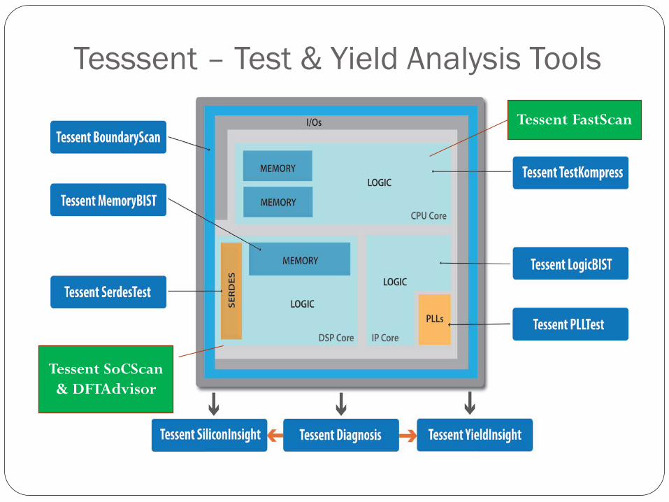
Tesssent – Test & Yield Analysis Tools
Tessent FastScan
Tessent SoCScan & DFTAdvisor

Mentor Graphics “Tessent” Products Tessent Fastscan – ATPG and Fault Simulation Fault models supported: stuck-at, IDDQ, transition, path delay and
bridge. Tessent SoC Scan (insert hierarchical scan) Absorbs functionality of older DFTAdvisor
Tessent DFTAdvisor – insert full/partial scan and test ckts Also: Tessent TestKompress (ATPG for scan tests) Tessent Boundary Scan (IEEE 1149.1) Tessent LogicBIST Tessent MemoryBIST Tessent Diagnosis (failure diagnosis) Tessent YieldInsight (statistical analysis of diagnosis data to find
systematic yield limiters)
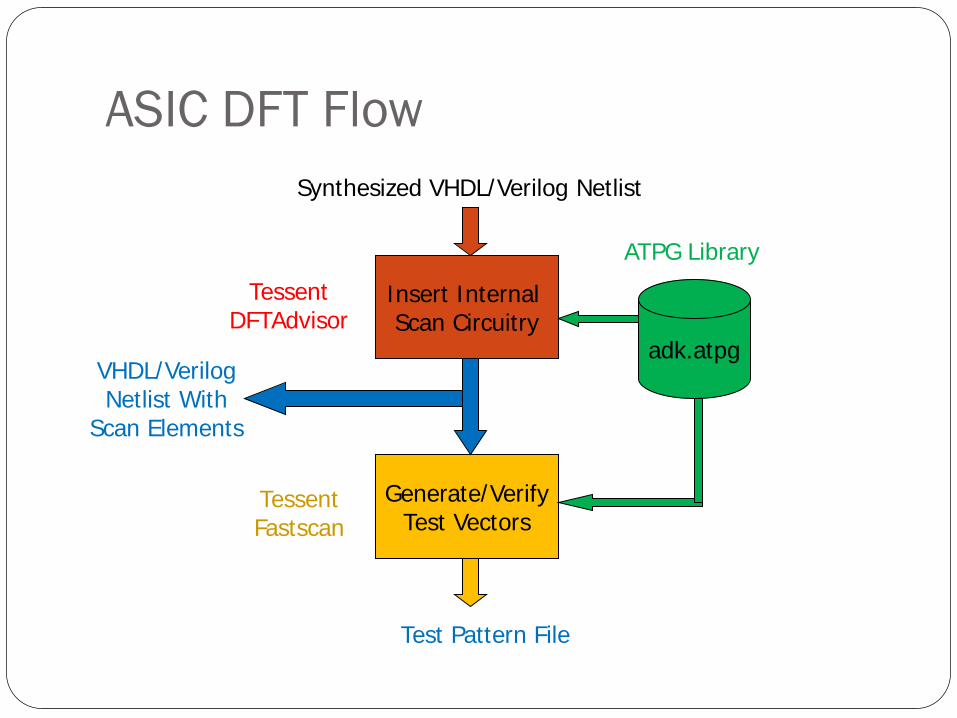
ASIC DFT Flow
Insert Internal Scan Circuitry
Generate/Verify Test Vectors
Synthesized VHDL/Verilog Netlist
adk.atpg
ATPG Library
Tessent DFTAdvisor
Tessent Fastscan
VHDL/Verilog Netlist With
Scan Elements
Test Pattern File
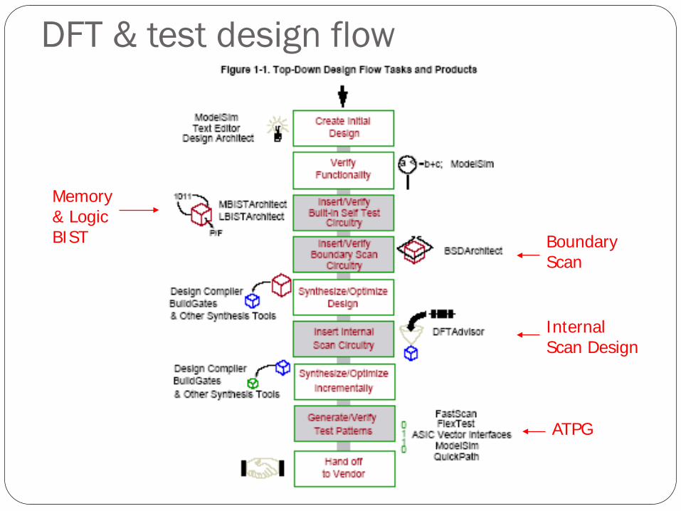
DFT & test design flow
Memory & Logic BIST Boundary
Scan
Internal Scan Design
ATPG

DFTadvisor/FastScan Design Flow
Source: FlexTest Manual
DFT/ATPG Library: adk.atpg
count4.vhd
count4_0.vhd count4.v
count4_scan.v
Leonardo

Example DFTadvisor script (Chan Hao)
dftadvisor –verilog count4.v –lib $ADK/technology/adk.atpg analyze control signals -auto_fix set scan type mux_Scan set system mode dft setup scan identification full_scan run //here you can determine how many scan chains you want to create insert test logic -scan on -number 3 //another way to create scan chains by giving maximum scan chain length //insert test logic -scan on -max_length 30 write netlist s1423_scan.v -verilog -replace //write dofile and procedure file for fastscan write atpg setup s1423_scan -procfile -replace exit

count4 – without scan design

count4 – scan inserted by DFTadvisor
Scan Control
Scan In
Scan FF
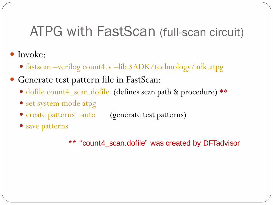
ATPG with FastScan (full-scan circuit)
Invoke: fastscan –verilog count4.v –lib $ADK/technology/adk.atpg
Generate test pattern file in FastScan: dofile count4_scan.dofile (defines scan path & procedure) ** set system mode atpg create patterns –auto (generate test patterns) save patterns
** “count4_scan.dofile” was created by DFTadvisor
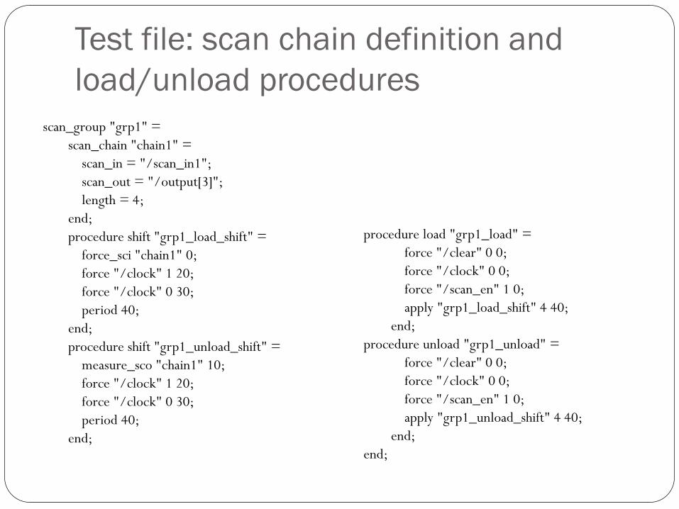
Test file: scan chain definition and load/unload procedures
scan_group "grp1" = scan_chain "chain1" = scan_in = "/scan_in1"; scan_out = "/output[3]"; length = 4; end; procedure shift "grp1_load_shift" = force_sci "chain1" 0; force "/clock" 1 20; force "/clock" 0 30; period 40; end; procedure shift "grp1_unload_shift" = measure_sco "chain1" 10; force "/clock" 1 20; force "/clock" 0 30; period 40; end;
procedure load "grp1_load" = force "/clear" 0 0; force "/clock" 0 0; force "/scan_en" 1 0; apply "grp1_load_shift" 4 40; end; procedure unload "grp1_unload" = force "/clear" 0 0; force "/clock" 0 0; force "/scan_en" 1 0; apply "grp1_unload_shift" 4 40; end; end;
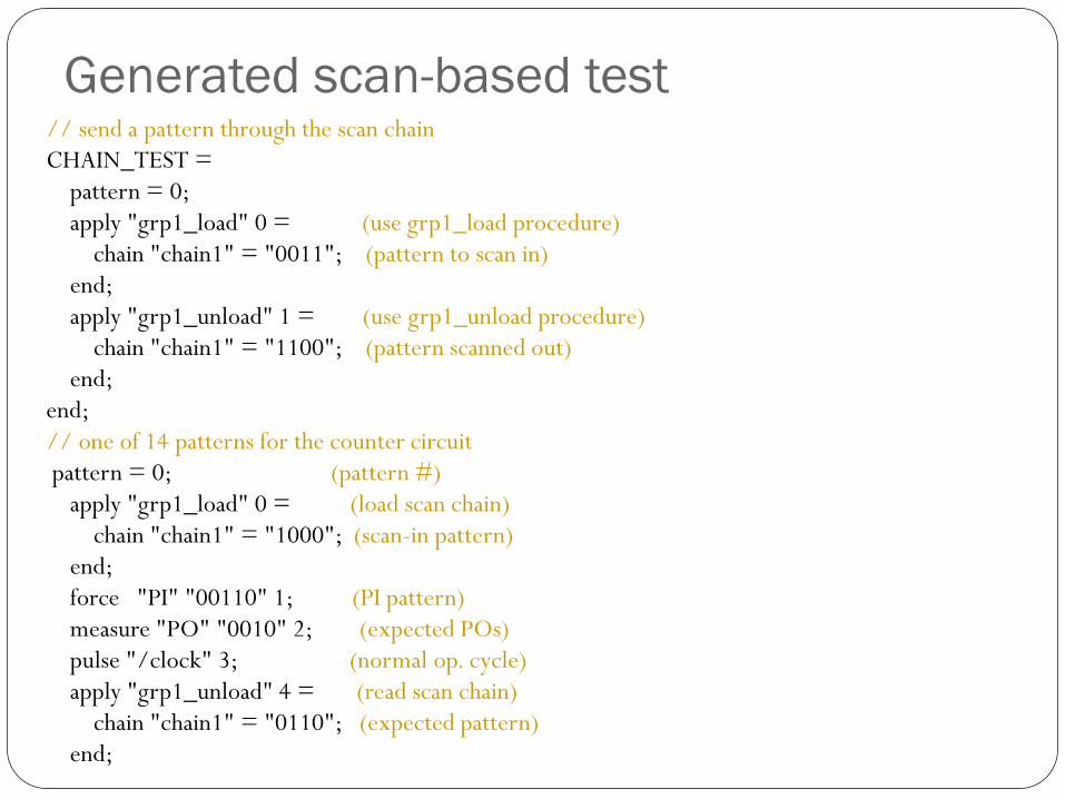
Generated scan-based test // send a pattern through the scan chain CHAIN_TEST = pattern = 0; apply "grp1_load" 0 = (use grp1_load procedure) chain "chain1" = "0011"; (pattern to scan in) end; apply "grp1_unload" 1 = (use grp1_unload procedure) chain "chain1" = "1100"; (pattern scanned out) end; end; // one of 14 patterns for the counter circuit pattern = 0; (pattern #) apply "grp1_load" 0 = (load scan chain) chain "chain1" = "1000"; (scan-in pattern) end; force "PI" "00110" 1; (PI pattern) measure "PO" "0010" 2; (expected POs) pulse "/clock" 3; (normal op. cycle) apply "grp1_unload" 4 = (read scan chain) chain "chain1" = "0110"; (expected pattern) end;

ASIC Physical Design (Standard Cell) (can also do full custom layout)
Floorplan Chip/Block
Place & Route Std. Cells
Component-Level Netlist (EDDM format)
IC Mask Data
Design Rule Check
Std. Cell Layouts
Mentor Graphics “IC Station”
(Linux cmd: adk_ic)
Mach TA/Eldo Simulation Model
Backannotate Schematic
Generate Mask Data
Layout vs. Schematic
Check
Design Rules
Process Data
Libraries
Calibre Calibre Calibre
ICblocks

Cell-Based IC
I/O pads
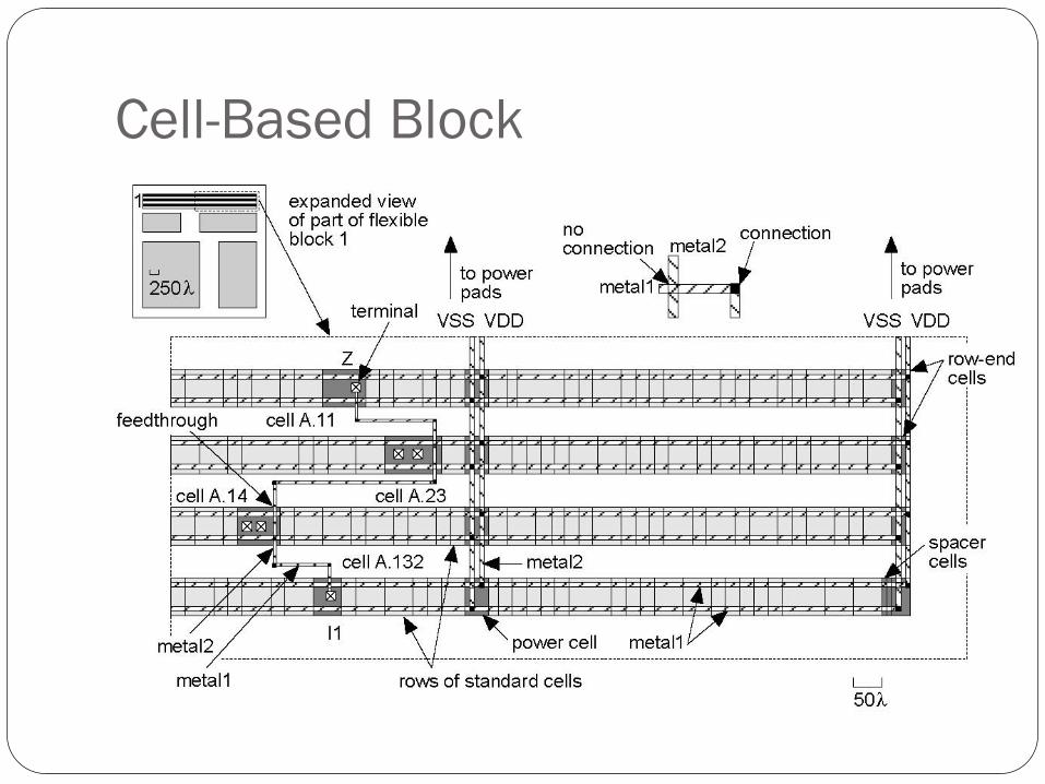
Cell-Based Block
Source: Weste “CMOS VLSI Design”
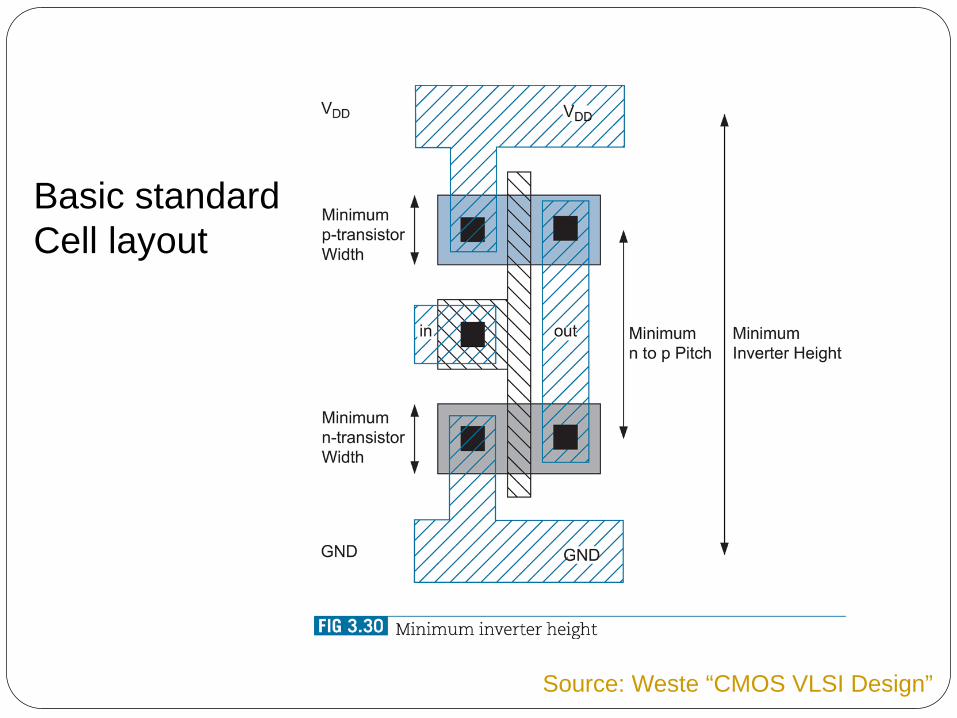
Basic standard Cell layout

Preparation for Layout 1. Use Design Architect-IC to convert Verilog netlist to Mentor
Graphics EDDM netlist format Invoke Design Architect-IC (adk_daic) On menu bar, select File > Import Verilog
Netlist file: count4.v (the Verilog netlist) Output directory: count4 (for the EDDM netlist) Mapping file $ADK/technology/adk_map.vmp
2. Open the generated schematic for viewing Click Schematic in DA-IC palette Select schematic in directory named above (see next slide) Click Update LVS in the schematic palette to create a netlist to be used later by
“Calibre” 3. Create design viewpoints for ICstation tools
adk_dve count4 –t tsmc035 (V.P’s: layout, lvs, sdl, tsmc035) Can also create gate/transistor schematics directly in DA-IC using
components from the ADK library

DA-IC generated schematic
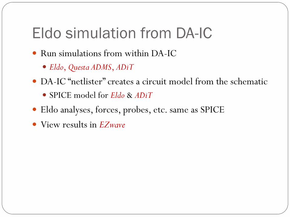
Eldo simulation from DA-IC Run simulations from within DA-IC Eldo, Questa ADMS, ADiT
DA-IC “netlister” creates a circuit model from the schematic SPICE model for Eldo & ADiT
Eldo analyses, forces, probes, etc. same as SPICE View results in EZwave
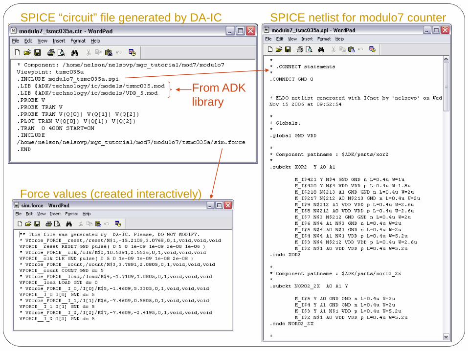
SPICE netlist for modulo7 counter SPICE “circuit” file generated by DA-IC
Force values (created interactively)
From ADK library
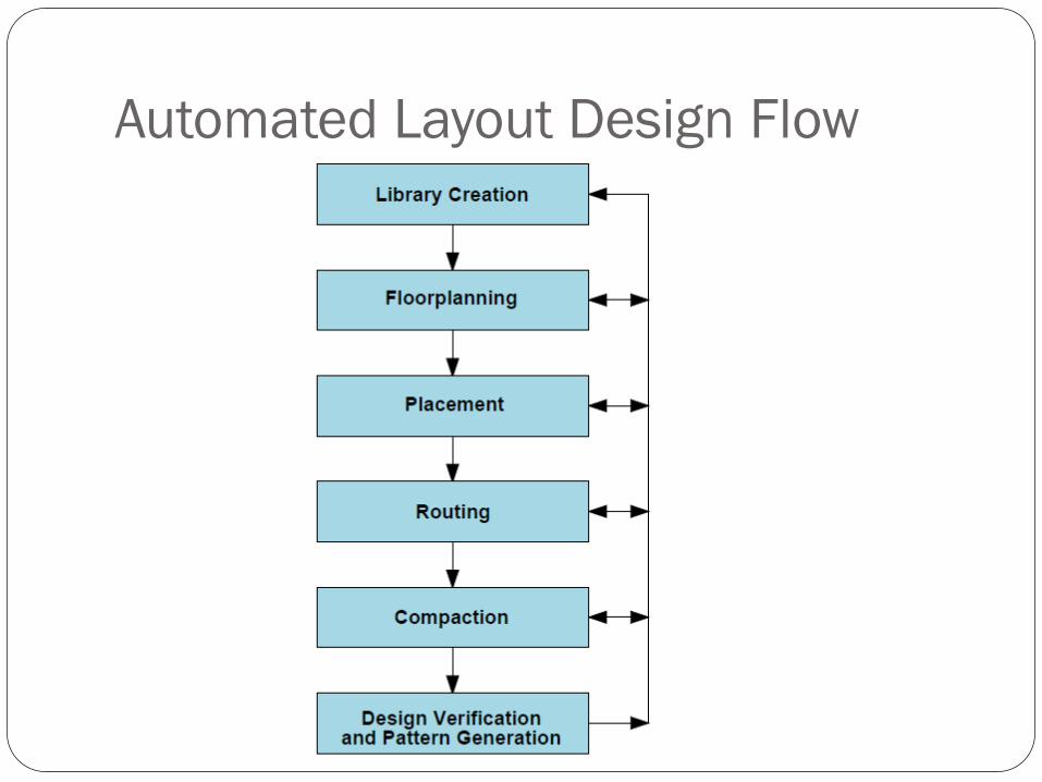
Automated Layout Design Flow

IC Station create cell dialog box (Linux command: adk_ic)
$ADK/technology/ic
Use schematic to drive layout
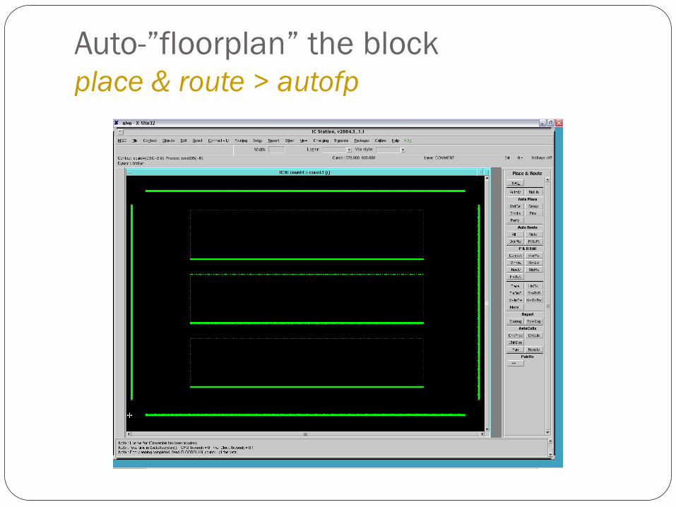
Auto-”floorplan” the block place & route > autofp
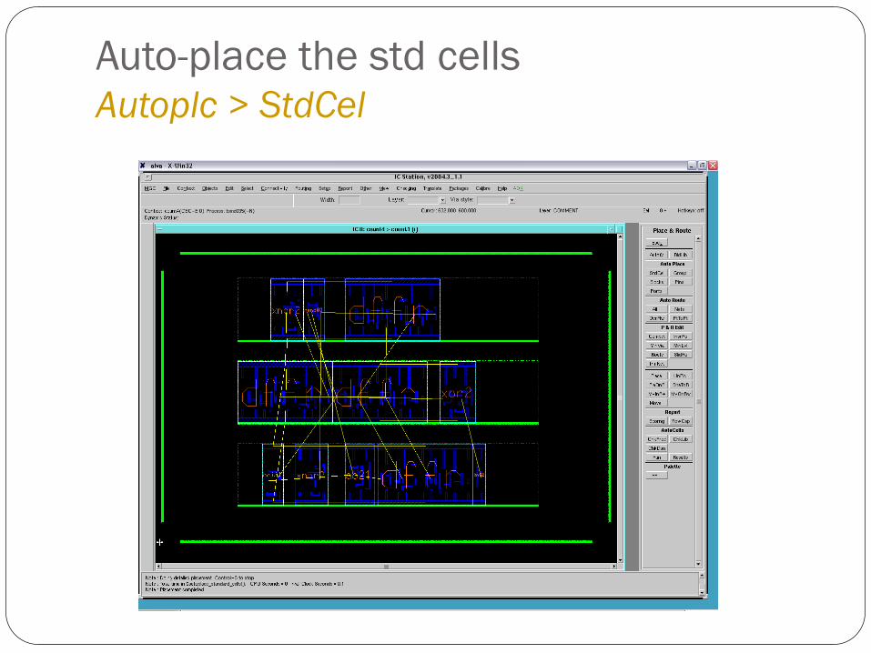
Auto-place the std cells Autoplc > StdCel
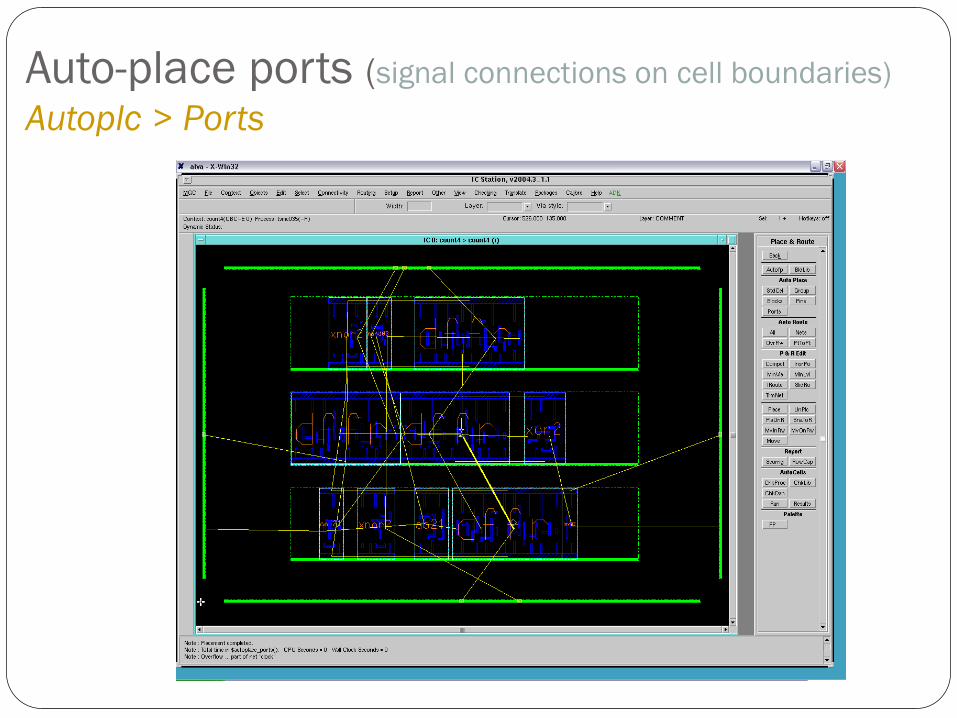
Auto-place ports (signal connections on cell boundaries) Autoplc > Ports
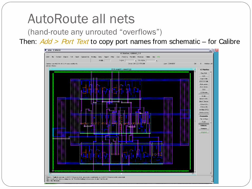
AutoRoute all nets (hand-route any unrouted “overflows”)
Then: Add > Port Text to copy port names from schematic – for Calibre
Layout design rule check (DRC)
Technology-specific design rules specify minimum sizes, spacing, etc. of features to ensure reliable fabrication Design rules file specified at startup Ex. tsmc035.rules
From main palette, select ICrules Click Check and then OK in prompt box (optionally select a specific area to check) Rules checked in numeric order

Common errors detected by DRC
To fix, click on First in palette to highlight first error Error is highlighted in the layout Click View to zoom in to the error (see next) Example: DRC9_2: Metal2 spacing = 3L Fix by drawing a rectangle of metal2 to fill in the gap between
contacts that should be connected Click Next to go to next error, until all are fixed NOTE: MOSIS will not fabricate a chip with DRC errors –
they perform their own DRC.
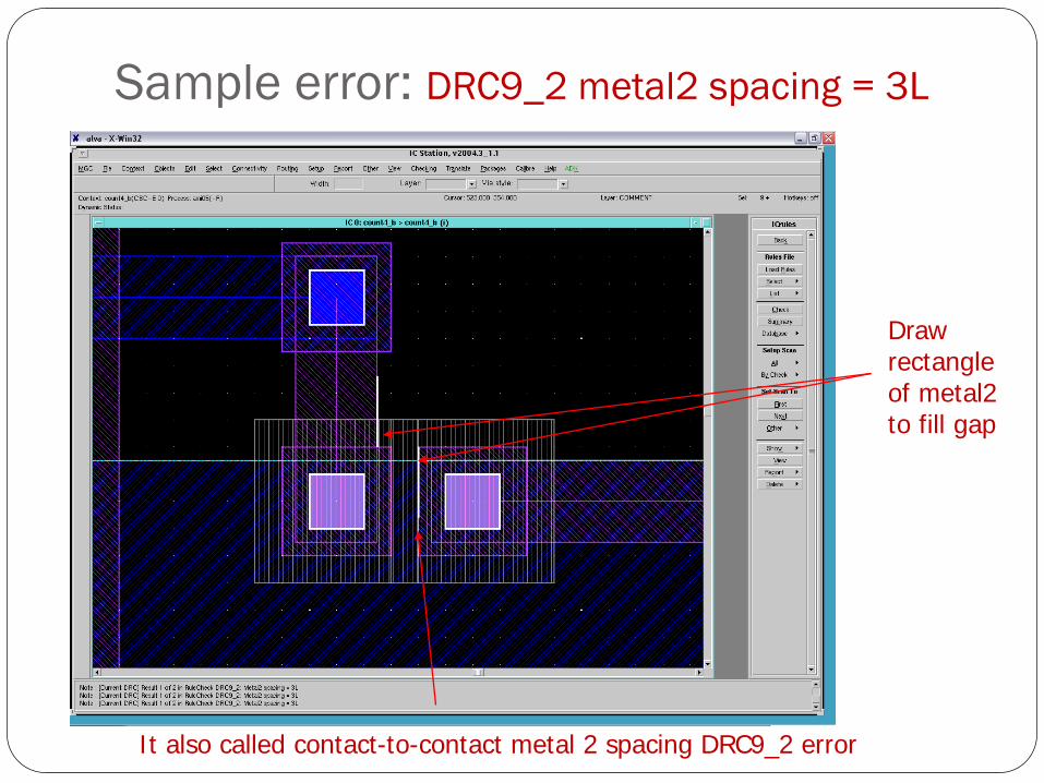
Sample error: DRC9_2 metal2 spacing = 3L
Draw rectangle of metal2 to fill gap
It also called contact-to-contact metal 2 spacing DRC9_2 error
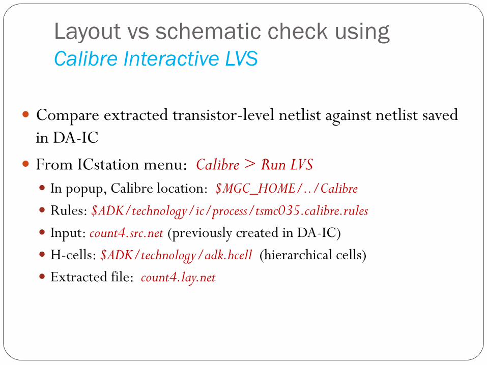
Layout vs schematic check using Calibre Interactive LVS
Compare extracted transistor-level netlist against netlist saved in DA-IC
From ICstation menu: Calibre > Run LVS In popup, Calibre location: $MGC_HOME/../Calibre Rules: $ADK/technology/ic/process/tsmc035.calibre.rules Input: count4.src.net (previously created in DA-IC) H-cells: $ADK/technology/adk.hcell (hierarchical cells) Extracted file: count4.lay.net
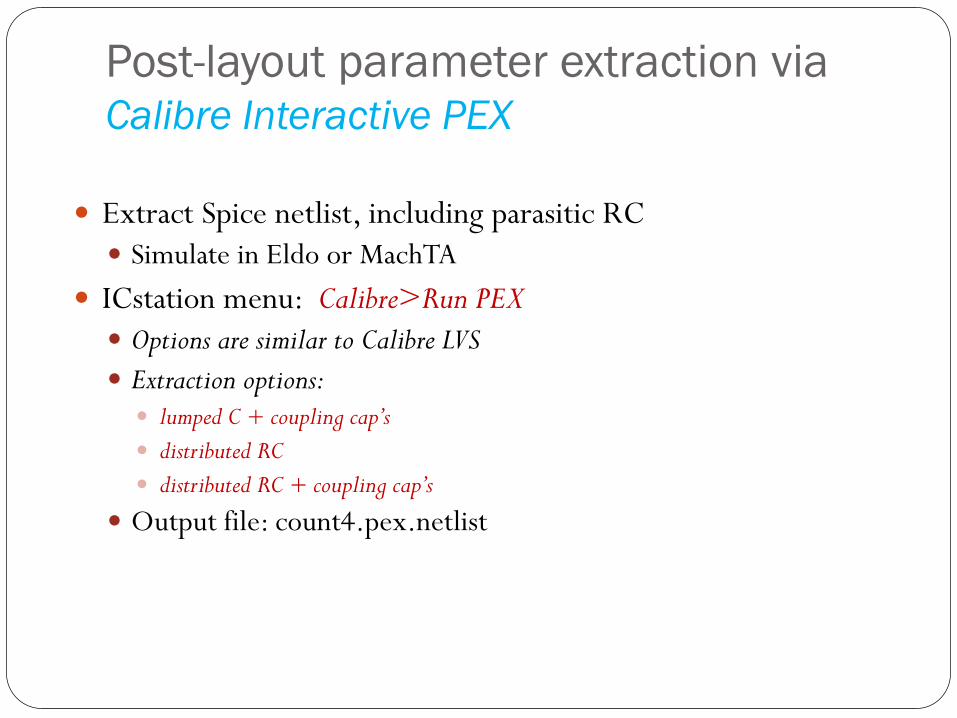
Post-layout parameter extraction via Calibre Interactive PEX
Extract Spice netlist, including parasitic RC Simulate in Eldo or MachTA
ICstation menu: Calibre>Run PEX Options are similar to Calibre LVS Extraction options: lumped C + coupling cap’s distributed RC distributed RC + coupling cap’s
Output file: count4.pex.netlist

Post-layout simulation: ADiT
• Fast-SPICE simulator • Analog & mixed-signal • 10X to 100X faster than other SPICE simulators • Integrated with Questa •Examples: $MGC_AMS_HOME/examples/adit/
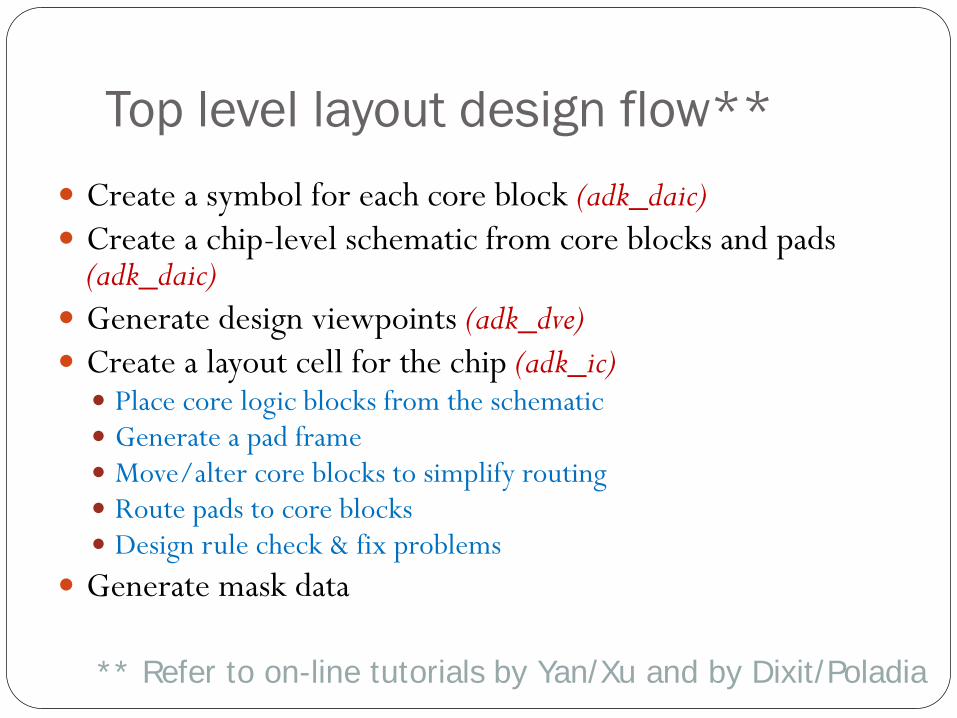
Top level layout design flow** Create a symbol for each core block (adk_daic) Create a chip-level schematic from core blocks and pads
(adk_daic) Generate design viewpoints (adk_dve) Create a layout cell for the chip (adk_ic) Place core logic blocks from the schematic Generate a pad frame Move/alter core blocks to simplify routing Route pads to core blocks Design rule check & fix problems
Generate mask data
** Refer to on-line tutorials by Yan/Xu and by Dixit/Poladia

Chip-level schematic (1) Generate a symbol for each “core” logic block In DA-IC, open the schematic (eg. modulo7) Select: Miscellaneous > Generate Symbol Add “phy_comp” property to the symbol Select the body of the symbol From the popup menu: Properties > Add
Enter property name: phy_comp Enter property value: mod7b
(layout cell name for the block created in IC Station)
Check & save
Example on next slide
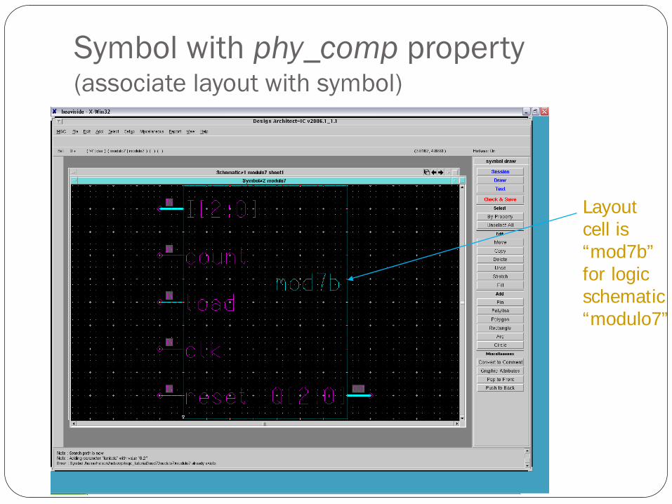
Symbol with phy_comp property (associate layout with symbol)
Layout cell is “mod7b” for logic schematic “modulo7”
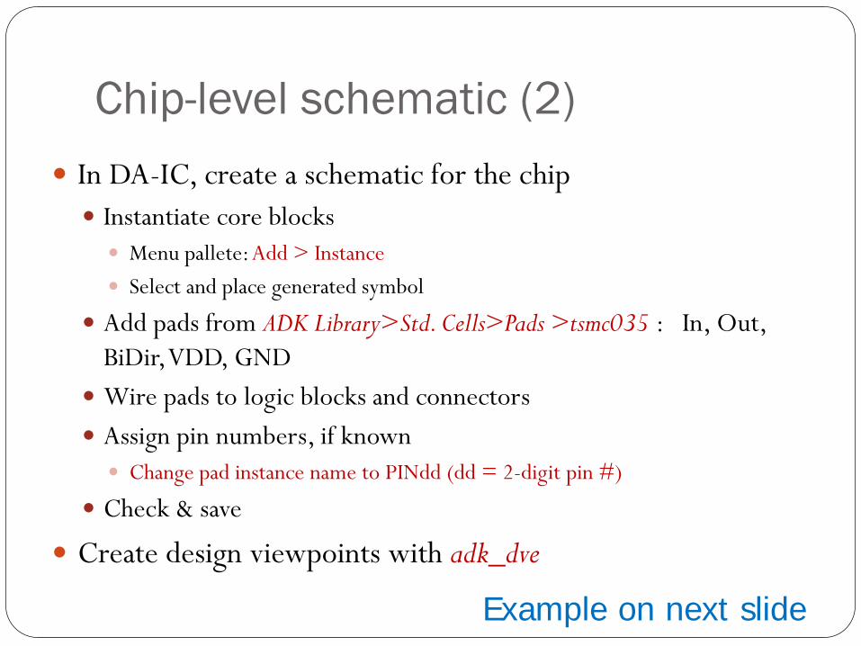
Chip-level schematic (2) In DA-IC, create a schematic for the chip Instantiate core blocks Menu pallete: Add > Instance Select and place generated symbol
Add pads from ADK Library>Std. Cells>Pads >tsmc035 : In, Out, BiDir, VDD, GND
Wire pads to logic blocks and connectors Assign pin numbers, if known Change pad instance name to PINdd (dd = 2-digit pin #)
Check & save
Create design viewpoints with adk_dve
Example on next slide
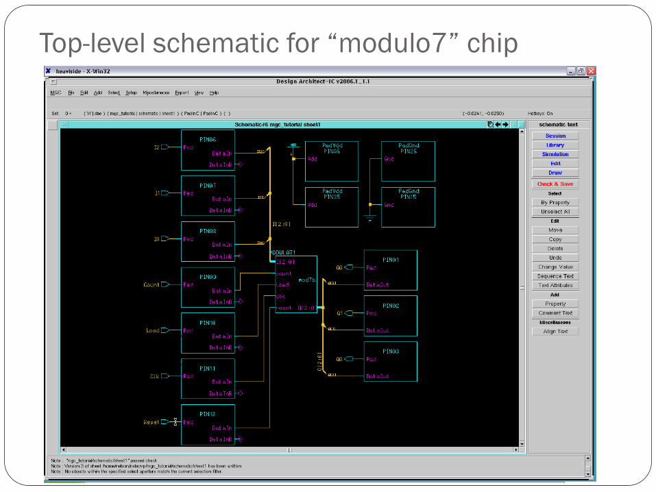
Top-level schematic for “modulo7” chip
Hierarchical connectors on “Pad” pins
Wire block I/O pins to pad signal pins
VDD/GND Pads
Core block
Instance name = PINxx (chip pin #)
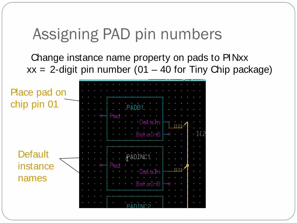
Assigning PAD pin numbers Change instance name property on pads to PINxx
xx = 2-digit pin number (01 – 40 for Tiny Chip package)
Place pad on chip pin 01
Default instance names

Top-level chip layout Start IC Station (adk_ic) & create a new layout cell enter cell name logic source is “layout” viewpoint of chip schematic same library, process file, rules file, and options as standard cell layout
Open the schematic ADK Edit menu: Logic Source > Open In the schematic, select all core cells (but not pads) Place the cells: Place > Inst
Generate the pad frame Top menu bar: ADK > Generate Padframe > tsmc035 (Only: AMI 1.2um, AMI 0.5um, TSMC 0.35um)

Chip layout (2) Move, rotate, flip core logic cells as desired to make routing
easier DO NOT EDIT OR MOVE PAD CELLS
Autoroute all connections Select autoroute all on P&R menu Click “options” on prompt bar, and unselect “Expand Channels”
(prevents pads from being moved) Add missing VDD/GND wires, if necessary Autorouter might only create 1 VDD/GND wire, even if multiple
VDD/GND pads Manually add others: Objects>Add>Path VDD/GND net width = 50 VDD/GND net vias = 6x6 (copy an existing via)

Modulo-7 counter in pad frame