Embed Size (px)
Citation preview
Computer Architecture for Digital Signal Processing
JONATHAN ALLEN, FELLOW, IEEE
Invited Paper
In this paper, a comprehensive overview of Computer Architec- ture for Digital Signal Processing is given. Such architectures are seen as the result of constraining influences from the nature of digital signal processing algorithms, architectural technfques includ ing appropriate choice of primitive elements, the underlying digital system technology, and programming languages for digital signal processing. Following a consideration of these influences, several examples are given ranging from chips through board level processors, to attached support processors with very high through- put. Trends for the future are discussed throughout the paper.
I . INTRODUCTION
Over the last 50 years, there has been an astonishing change in both the nature of signal processing algorithms and the computational means utilized to exercise them [I]. Starting before World War I I , there was a period of classical signal processing characterized by static realizations of low-pass, band-pass, and high-pass filters that used only gross knowledge of signal and noise spectra. Signal and noise statistics were not utilized, and most of the imple- mentations utilized analog technology. It was common- place to design all-pole IIR filters, such as Butterworth, Chebyschev, and elliptic designs, and the primary oper- ations were differentiation and integration. Computa- tionally, these techniques were characterized by taking order of N (O(N)) processing time, where N is the number of sample points of the signal being processed at any given time. Following the Second World War, many applications, such as vocoders, that had been implemented in analog form became so complex that it was difficult to explore the effect on system performance of the variation of many design parameters. For this reason, digital signal processing was introduced at first as a simulation technique, with no thought paid to its utility in direct real-time applications, since the technology to support this usage was not avail- able. During this epoch, there was a more refined manipu-
Manuscript received April 16, 1984; revised January 25, 1985. This work was supported by AFOSR under Contract F4%20-84Mxll.
The author is with the Research Laboratory of Electronics and the Department of Electrical Engineering and Computer Science, Mas- sachusetts Institute of Technology, Cambridge, MA 02139, USA.
ool8-9219/8S/05~52sol.00 Wl985 IEEE
lation of data spectra using limited knowledge of signal and noise statistics, such as matched and Wiener filters. While statistics were utilized, they did not vary with time, nor was any model introduced for the way in which data were generated. As time progressed, implementations became primarily digital, and all-zero FIR digital filters were intro- duced. The primary operations performed, in addition to filtering previously mentioned, included convolution, corre- lation, and efficient techniques for computing the discrete Fourier transform such as the FFT. Corresponding to these operations, the computational complexity involved was of order N2 or Nlog, N, as contrasted to the previous linear dependence on N. Finally, in the present epoch, lasting so far for approximately 20 years, sophisticated manipulation of data spectra using detailed knowledge of signal and noise statistics has been introduced as exemplified by adap- tive and Kalman filters. For these systems, statistics can vary with time, and additional structure was imposed by assum- ing models on how data are generated, such as the linear predictive coding model used in speech. As the technology improved, implementations became realized digitally for complex systems, taking advantage of the precision, repeat- ability, high signal-to-noise ratio, and flexibility afforded by digital systems. Time-varying digital filters were introduced, and matrix difference equations appeared. Primary oper- ations were extended beyond the previous emphasis on convolution and Fourier transforms to matrix-vector multi- plication, matrix-matrix multiplication, linear system solu- tion, least squares solution, and eigenvalue decomposition. Algorithms for these tasks are characterized by order @ processing time, thus putting great demand on effective computational means for realization of these systems.
From this brief view over the evolving nature of the field, it is clear that the complexity of digital signal processing tasks has risen markedly, following not only theoretical advances, but also the rapid advances in integrated circuit technology. Clearly, an agent is needed to coordinate the theoretical approaches with the ambient technology, and this task has fallen to computer architecture in the large, but due to the specialized nature of the algorithms per- formed in digital signal processing, specialized processors have evolved for most of these tasks. The range of applica-
85 2 PROCEEDINGS OF THE IEEE, VOL. 73, NO. 5, M A Y 1985
tions, originally focused around low-bandwidth speech ap- plications, has extended dramatically, and has required all of the performance that contemporary computing systems can deliver, yet at reasonable cost. The techniques used for characterizing computer architecture for digital signal processing are not disjoint from those used for computer architecture in the large, but the emphasis on various fea- tures may vary in order to satisfy application requirements.
The performance of digital computer systems has two contrasting facets. On the one hand, greater computational throughput can be achieved by improvements in circuit performance, and this area is largely driven by the technol- ogy that is available at any given time. It is probably safe to say that most manufacturers would prefer to achieve the desired performance level through utilization of con- ventional single-sequence computer architectures with state-of-the-art technology. Additional throughput can be achieved, however, through exploitation of the parallelism inherent in many digital signal processing tasks. Happily, many of these tasks provide such a large amount of parallel- ism that it has only recently been completely exploited even for algorithms that have been in use for some time. We will discuss the many means by which this parallelism can be translated into computational structures, observing that the combination of aggressive technology and innova- tive highly parallel architectures can lead to processing rates in excess of 200 million floating-point operations per sec- ond (megaflops) for 32-bit operands. This is certainly a startling level of performance, and one that opens up the practical utilization of even the most complex theoretical signal processing approaches.
In this paper, we give a comprehensive overview of those factors that constrain the nature of computer architecture for digital signal processing. We start with a fundamental view of the nature of algorithms, including their means of representation, and give a view of many of the most signifi- cant calculations that must be performed, thus revealing not only the primitive computational means that must be made available, but the architectural structures that can utilize them with particular attention to the level of paral- lelism. Following this view of algorithms, we move on to an establishment of a general framework for computer archi- tectures that will allow us to examine the nature of parallel- ism along data paths together with its concomitant control in an abstract form that is not encumbered by implementa- tion details. This framework will then lead to an examina- tion of a set of techniques that comprise “architectural exploration,” whereby the system designer may systemati- cally move over the design space of possible architectures to select the desired performance level. A comprehensive categorization of the means for utilizing contemporary in- tegrated circuit technology with a variety of architectural styles is given, permitting a broad view of the space of high-performance computer systems. Next, an assessment of integrated circuit technology is given, including both bipolar and MOS technologies, together with their impact on canonical circuits, interconnect, and packaging. In this section of the paper, we also give a view of integrated circuit design, ranging from utilization of off-the-shelf cir- cuits through semicustom techniques to full custom design, since there is a great deal of innovation for new complex special-purpose signal processing integrated circuits, Hav- ing examined the nature of digital signal processing al-
gorithms, architectures, and supporting technology, we focus on programming techniques, a factor often ignored in early designs but now seen as essential for the viability of modern processors. Next, we examine a variety of specific designs, ranging from canonical circuit functions through digital signal processing chips, wafer-scale systems, at- tached processors, stand-alone programmable machines, systolic arrays, and linear-algebra architectures. We end by establishing a uniform view over all of these developments leading to a reasoned set of expectations for future pro- gress. This is a highly volatile and exciting area, bringing together rich theoretical investigations, burgeoning tech- nology, innovative architectural synthesis, and an unending demand from applications for improved performance. It is our intention to convey the way in which these wide-rang- ing forces are coalescing into a cohesive set of new perfor- mance strategies, often yielding well over a factor of a thousand improvement over even the fastest general-pur- pose machines.
II. ALGORITHMS
In this section we examine the nature of the algorithms that characterize the tasks to be performed in digital signal processing. The complementary aspects of architecture and architectural units, technology, and data and programming structures, are often seen as posing representation issues associated with the nature of the particular implementa- tion, but it must be emphasized that there is a fundamental problem associated with the representation of algorithms themselves. From the point of view of system design, it would be useful to be able to specify and separate what an algorithm does from how i t is performed. This separation is sometimes referred to as the competence/performance dis- tinction, and it remains a discouraging fact that there is no means available to specify task competence separately from task performance over a broad range of tasks. Thus for example, a set of simultaneous linear equations specifies all of the constraints that have to hold for any solution to these equations, but it is neutral with respect to indicating a performance strategy for the solution of these equations, such as Gaussian elimination. Constraint representations have been proposed [2] for this iimited class of systems, but they are not available over other task domains of interest to digital signal processing. With this observation in mind, we must proceed with the knowledge that any algorithm to be used in a digital signal processing system inevitably con- founds a particular performance bias with the intrinsic nature of the algorithmic competence. This means that it is impossible to even state an algorithm without including a performance bias, a fact which can be readily appreciated by the examination of any textbook on algorithms. Even the graphic nature of algorithmic representation carries with it performance biases, including the use of procedural forms, such as linear recurrence equations, as well as structural forms such as signal flow graphs. In this paper, we will introduce and utilize both equations and signal flow repre- sentations, choosing each form for its insightfulness where appropriate. While we will discuss later the possibility of the use of functional languages, we will utilize here these more conventional representations, even though we must emphasize to the reader that a heightened awareness to the
ALLEN: COMPUTER ARCHITECTURE F O R DIGITAL SIGNAL PROCESSING 853
possibility of latent parallelism must be retained in ex- amining all of these forms.
We start our discussion of algorithmic structures by citing the forms used for infinite impulse response and finite impulse response filters. In the case of infinite impulse response filters, the basic building block frequently pro- vided is the so-called "second-order section" shown in (1)
y( n) = AY( n - I) + BY( n - 2) + Cx( n - 2)
+ D x ( n - 1) + x ( . ) . (1)
In the most general form of the second-order section, the two previous values of both the input and the output must be multiplied by real coefficients. Thus there is an oppor- tunity to perform as many as four multiplications in parallel, the results of which must then be summed with the tapped current input. In the case of finite impulse response filters, the input sample stream is tapped after a succession of delays, each tapped value being multiplied by a tap coeffi- cient, and then all of these products are summed to pro- duce the output. It i s not uncommon to have several hundred such taps. Once again, it is clear that the algorith- mic requirement is to compute a sum-of-products. A variety of techniques for effecting this calculation will be discussed in the sequel.
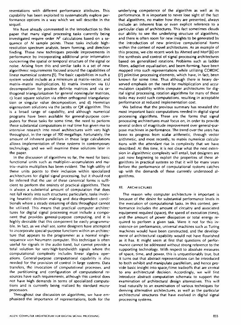
Another fundamental algorithm, used repeatedly in many applications, is the well-known discrete Fourier transform (DFT), which is often implem'ented as the fast Fourier transform (FFT). The calculation to be performed is shown in (2)
N-1
X k = x n W k , O g k g N - I (2) n - 0
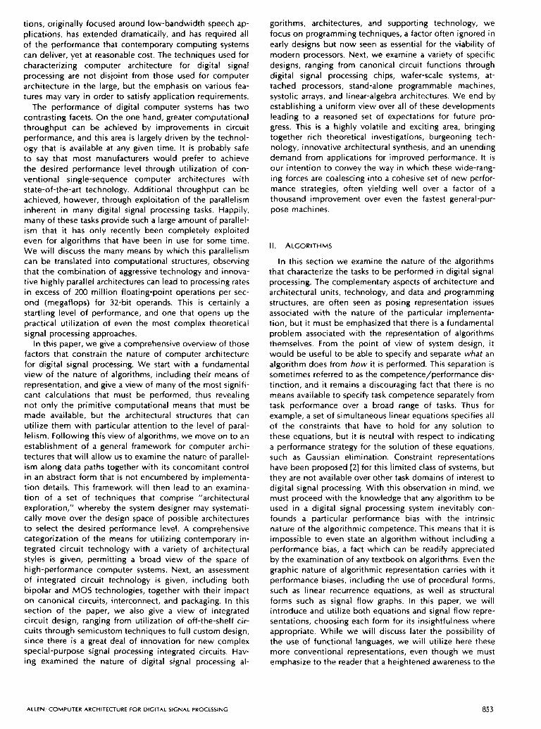
where. the output values x k are obtained by summing the products obtained by multiplying the input sample values x , by the complex value W k = exp(jZn/N)"". These com- plex products, X,,Wk, can be formed from four real multi- plies and two adds. Straightforward calculation of the DFT as a sum of complex products, however, misses much of the inherent structure of the FFT algorithm, which is best seen graphically as in Fig. 1. In this representation, an eight-point
FFT, N = 8
f
8 l o g , N BUTTERFLIES
Fig. 1. Eight-point FET, illustrating decomposition into twelve butterflies.
FFT is decomposed into three (= log2@ vertical arrays, each of which involves the calculation of four "butterflies," which are the modular "heart" of the algorithm.
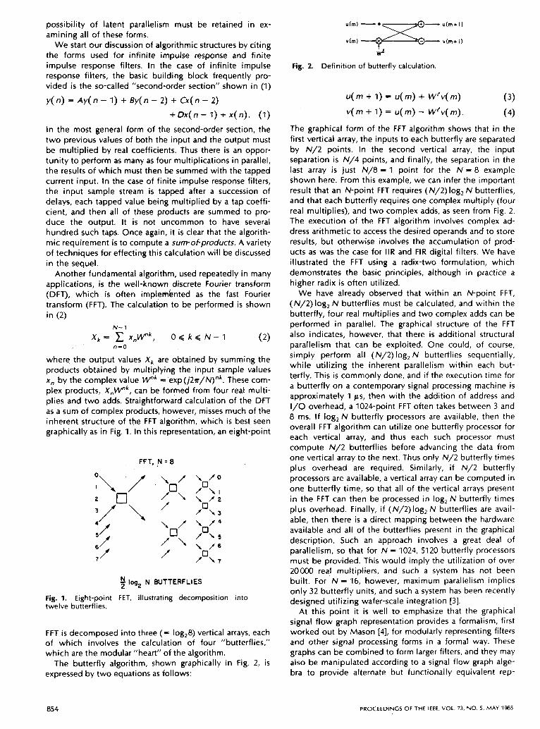
The butterfly algorithm, shown graphically in Fig. 2, is expressed by two equations as follows:
u(m) - v(m)
Fig. 2. Definition of butterfly calculation.
u ( m + I ) = u ( r n ) + W ' v ( m ) (3)
v( m + I) = u( m) - ~ ' v ( m ) , ( 4)
The graphical form of the FFT algorithm shows that in the first vertical array, the inputs to each butterfly are separated by N/2 points. In the second vertical array, the input separation is N/4 points, and finally, the separation in the last array i s just N/8 = 1 point for the N = 8 example shown here. From this example, we can infer the important result that an N-point FFT requires (N/2) log, N butterflies, and that each butterfly requires one complex multiply (four real multiplies), and two complex adds, as seen from Fig. 2. The execution of the FFT algorithm involves complex ad- dress arithmetic to access the desired operands and to store results, but otherwise involves the accumulation of prod- ucts as was the case for IIR and FIR digital filters. We have illustrated the FFT using a radix-two formulation, which demonstrates the basic principles, although in practice a higher radix is often utilized.
We have already observed that within an N-point FFT, (N/2)log2 N butterflies must be calculated, and within the butterfly, four real multiplies and two complex adds can be performed in parallel. The graphical structure of the FFT also indicates, however, that there is additional structural parallelism that can be exploited. One could, of course, simply perform all (N/2) log, N butterflies sequentially, while utilizing the inherent parallelism within each but- terfly. This is commonly done, and if the execution time for a butterfly on a contemporary signal processing machine is approximately 1 ps, then with the addition of address and 1/0 overhead, a 1024-point FFT often takes between 3 and 8 ms. If log, N butterfly processors are available, then the overall FFT algorithm can utilize one butterfly processor for each vertical array, and thus each such processor must compute N/2 butterflies before advancing the data from one vertical array to the next. Thus only N/2 butterfly times plus overhead are required. Similarly, if N/2 butterfly processors are available, a vertical array can be computed in one butterfly time, so that all of the vertical arrays present in the FFT can then be processed in log, N butterfly times plus overhead. Finally, if (N/2)log2 N butterflies are avail- able, then there is a direct mapping between the hardware available and all of the butterflies present in the graphical description. Such an approach involves a great deal of parallelism, so that for N = 1024, 5120 butterfly processors must be provided. This would imply the utilization of over 20000 real multipliers, and such a system has not been built. For N = 16, however, maximum parallelism implies only 32 butterfly units, and such a system has been recently designed utilizing wafer-scale integration [3].
At this point it is well to emphasize that the graphical signal flow graph representation provides a formalism, first worked out by Mason [4], for modularly representing filters and other signal processing forms in a formal way. These graphs can be combined to form larger filters, and they may also be manipulated according to a signal flow graph alge- bra to provide alternate but functionally equivalent rep-
854 PROCEEDINGS O F THE IEEE. VOL. 73, NO 5. M A Y 1985
resentations with different performance attributes. This capability has been exploited to systematically explore per- formance options in a way which we will describe in the sequel.
We have already commented in the Introduction to this paper that many signal processing tasks currently being investigated require order @ calculations based on a se- quence of N sample points. These tasks include high- resolution spectrum analysis, beam forming, and direction finding. These new techniques provide improvements in performance by incorporating additional prior information concerning the spatial or temporal structure of the signal or noise. Arising from this and similar tasks is a set of new algorithmic requirements focused around the capabilities of linear numerical systems [SI. The basic capabilities in such a system would include as a minimum a) matrix-vector, and matrix-matrix multiplication, b) matrix inversion via LU decomposition for positive definite matrices and via or- thogonal triangularization for general nonsingular matrices, c) least square solution via either orthogonal triangulariza- tion or singular value decomposition, and d) Hermitian eigensystem solutions via the Jacoby or QR algorithm. This is a broad range of capability, and although numerical programs have been available for general-purpose com- puters for these tasks for some time, the need to perform these substantial computations in real time has given rise to intensive research into novel architectures with very high throughput, in the range of 700 megaflops. Fortunately, the amount of inherent parallelism in these large calculations allows implementation of these systems in contemporary technology, and we will examine these solutions later in the paper.
In the discussion of algorithms so far, the need for basic functional units such as multiplier-accumulators and ma- trix-matrix multipliers has been evident. The high utility of these units points to their inclusion within specialized architectures for digital signal processing, but it should not be inferred that the use of these canonical forms is suffi- cient to perform the entirety of practical algorithms. There is always a substantial amount of computation that does not fall nicely into such structures; particularly, tasks involv- ing heuristic decision making and data-dependent condi- tionals where a steady streaming of data throughput cannot be utilized. This means that practical computer architec- tures for digital signal processing must include a cornpo- nent that provides general-purpose computing, and it is highly desirable that this component be easily programma- ble. In fact, as we shall see, some designers have attempted to incorporate special-purpose functions within an architec- ture that appears to the programmer as a normal single- sequence von Neumann computer. This technique is often useful for signals in the audio band, but cannot provide a total solution for very-high-bandwidth signals where the computational complexity includes linear algebra oper- ations. General-purpose computational capability is also needed for the provision of control in large systems. Data transfers, the invocation of computational processes, and the partitioning and configuration of computational re- sources have such requirements, although this control does not have high demands in terms of specialized computa- tions and is currently being realized by standard micro- processors.
Throughout our discussion on algorithms, we have em- phasized the importance of representations, both for the
underlying competence of the algorithm as well as i t s performance. it is important to never lose sight of the fact that algorithms, no matter how they are presented, always include an inherent bias or even explicit reference to a particular class of architectures. This fact sometimes clouds our ability to see the underlying structure of algorithms, and there is often room for new insights to be generated by the introduction of new primitive computational forms within the context of novel architectures. As an example of this process, we cite recent work by Ahmed and Morf [6] on the synthesis and control of signal processing architectures based on generalized rotations. Problems such as ladder filters, adaptive equalization, and beam forming, have been mapped into such representations while utilizing CORDIC (71 primitive processing elements, which have, in fact, been known for some time. Thus although there is heavy de- served emphasis on the need for multiplication and accu- mulation capability within computer architectures for dig- ital signal processing, rotation algorithms for many of these tasks may avoid such computations, resulting in acceptable performance at reduced implementation cost.
We believe that the previous summary has revealed the most important basic computations needed in digital signal processing algorithms. These are the forms that signal processing architectures must focus on, in order to provide several orders of magnitude improvement over general-pur- pose machines in performance The trend over the years has been to progress from scalar arithmetic, through vector arithmetic, and most recently, to matrix numerical calcula- tions with the attendant rise in complexity that we have described. At this time, it is not clear what the next exten- sion in algorithmic complexity will entail, but designers are just now beginning to exploit the properties of these al- gorithms in practical systems so that it will be many years before the performance of computational systems catches up with the demands of these currently understood al- gorithms.
Ill. ARCHITECTURES
The reason why computer architecture is important is because of the desire for substantial performance levels in the execution of computational tasks. In this context, per- formance includes the amount of circuitry and associated equipment required (space), the speed of execution (time), and the amount of power d'issipation or total energy re- quired to perform a given task. Were it not for this in- sistence on performance, universal machines such as Turing machines would have been constructed, and the develop- ment of architectural capability would not have flourished as it has. It might seem at first that questions of perfory mance cannot be addressed without strong reference to the supporting technology. With respect to absolute measures of space, time, and power, this is unquestionably true, but it turns out that abstract representations can be introduced to both exhibit and manipulate parallelism, and hence pro- vide basic insight into space/time tradeoffs that are central to any architectural decision. Accordingly, we will first introduce abstract computation schemata to support the examination of architectural design alternatives. This will lead naturally to an examination of various techniques for deriving alternative architectures, as well as the particular architectural structures that have evolved in digital signal processing systems.
ALLEN: COMPUTER ARCHITECTURE F O R DIGITAL SIGNAL PROCESSING 855
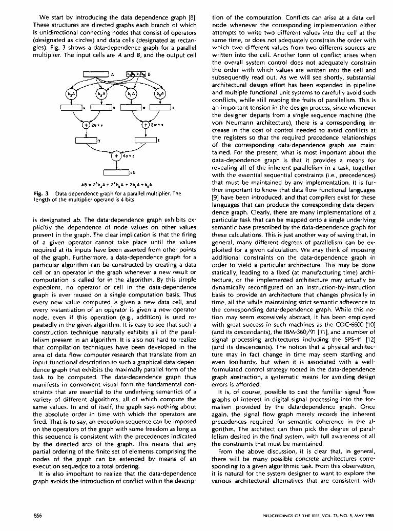
We start by introducing the data dependence graph [8]. These structures are directed graphs each branch of which is unidirectional connecting nodes that consist of operators (designated as circles) and data cells (designated as rectan- gles). Fig. 3 shows a data-dependence graph for a parallel multiplier. The input cells are A and B, and the output cell
7 + 4 y + z
AB = 2'b,A + 2'b2A + 2b,A + b,A
Fig. 3. Data dependence graph for a parallel multiplier. The length of the multiplier operand is 4 bits.
is designated ab. The data-dependence graph exhibits ex- plicitly the dependence of node values on other values present in the graph. The clear implication is that the firing of a given operator cannot take place until the values required at i t s inputs have been asserted from other points of the graph. Furthermore, a data-dependence graph for a particular algorithm can be constructed by creating a data cell or an operator in the graph whenever a new result or computation is called for in the algorithm. By this simple expedient, no operator or cell in the data-dependence graph is ever reused on a single computation basis. Thus every new value computed is given a new data cell, and every instantiation of an opsrator is given a new operator node, even i f this operation (e.g., addition) is used re- peatedly in the given algorithm. It is easy to see that such a construction technique naturally exhibits all of the paral- lelism present in an algorithm. It is also not hard to realize that compilation techniques have been developed in the area of data flow computer research that translate from an input functional description to such a graphical data-depen- dence graph that exhibits the maximally parallel form of the task to be computed. The data-dependence graph thus manifests in convenient visual form the fundamental con- straints that are essential to the underlying semantics of a variety of different algorithms, all of which compute the same values. In and of itself, the graph says nothing about the absolute order in time with which the operators are fired. That is to say, an execution sequence can be imposed on the operators of the graph with some freedom as long as this sequence is consistent with the precedences indicated by the directed arcs of the graph. This means that any partial ordering of the finite set of elements comprising the nodes of the graph can be extended by means of an execution seque ce to a total ordering.
It is also imp0 I t ant to realize that the data-dependence graph avoids the introduction of conflict within the descrip-
tion of the computation. Conflicts can arise at a data cell node whenever the corresponding implementation either attempts to write two different values into the cell at the same time, or does not adequately constrain the order with which two different values from two different sources are written into the cell. Another form of conflict arises when the overall system control does not adequately constrain the order with which values are written into the cell and subsequently read out. As we will see shortly, substantial architectural design effort has been expended in pipeline and multiple functional unit systems to carefully avoid such conflicts, while still reaping the fruits of parallelism. This is an important tension in the design process, since whenever the designer departs from a single sequence machine (the von Neumann architecture), there is a corresponding in- crease in the cost of control needed to avoid conflicts at the registers so that the required precedence relationships of the corresponding data-dependence graph are main- tained. For the present, what is most important about the data-dependence graph is that it provides a means for revealing all of the inherent parallelism in a task, together with the essential sequential constraints (i.e., precedences) that must be maintained by any implementation. It is fur- ther important to know that data flow functional languages [9] have been introduced, and that compilers exist for these languages that can produce the corresponding data-depen- dence graph. Clearly, there are many implementations of a particular task that can be mapped onto a single underlying semantic base prescribed by the data-dependence graph for these calculations. This is just another way of saying that, in general, many different degrees of parallelism can be ex- ploited for a given calculation. We may think of imposing additional constraints on the data-dependence graph in order to yield a particular architecture. This may be done statically, leading to a fixed (at manufacturing time) archi- tecture, or the implemented architecture may actually be dynamically reconfigured on an instruction-by-instruction basis to provide an architecture that changes physically in time, all the while maintaining strict semantic adherence to the corresponding data-dependence graph. While this no- tion may seem excessively abstract, it has been employed with great success in such machines as the CDC-6600 [IO] (and its descendants), the IBM-360/91 [Ill, and a number of signal processing architectures including the SPS-41 [I 21 (and its descendants). The notion that a physical architec- ture may in fact change in time may seem startling and even foolhardy, but when it is associated with a well- formulated control strategy rooted in the data-dependence graph abstraction, a systematic means for avoiding design errors is afforded.
It is, of course, possible to cast the familiar signal flow graphs of interest in digital signal processing into the for- malism provided by the data-dependence graph. Once again, the signal flow graph merely records the inherent precedences required for semantic coherence in the al- gorithm. The architect can then pick the degree of paral- lelism desired in the final system, with full awareness of all the constraints that must be maintained.
From the above discussion, it is clear that, in general, there will be many possible concrete architectures corre- sponding to a given algorithmic task. From this observation, it is natural for the system designer to want to explore the various architectural alternatives that are consistent with
856 PROCEEDINGS O F THE IEEE, VOL. 73, N O . 5 , M A Y 1985
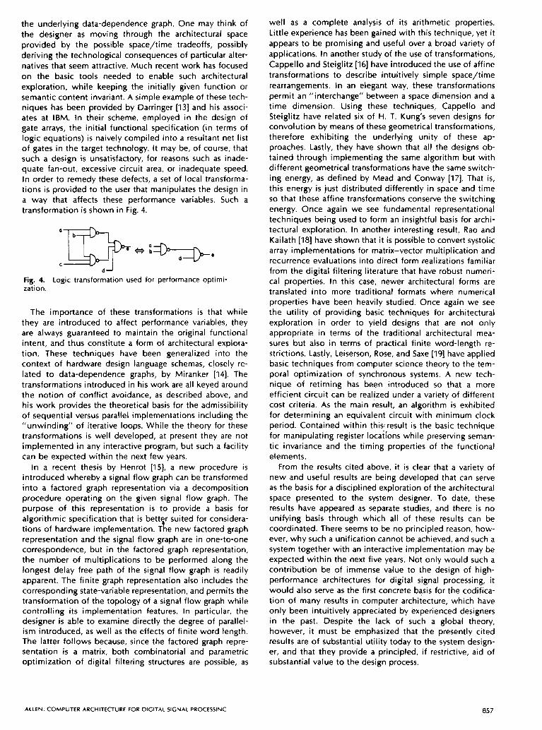
the underlying data-dependence graph. One may think of the designer as moving through the architectural space provided by the possible space/time tradeoffs, possibly deriving the technological consequences of particular alter- natives that seem attractive. Much recent work has focused on the basic tools needed to enable such architectural exploration, while keeping the initially given function or semantic content invariant. A simple example of these tech- niques has been provided by Darringer [I31 and his associ- ates at IBM. In their scheme, employed in the design of gate arrays, the initial functional specification (in terms of logic equations) is naively compiled into a resultant net list of gates in the target technology. It may be, of course, that such a design is unsatisfactory, for reasons such as inade- quate fan-out, excessive circuit area, or inadequate speed. In order to remedy these defects, a set of local transforma- tions is provided to the user that manipulates the design in a way that affects these performance variables. Such a transformation is shown in Fig. 4.
Fig. 4. Logic transformation used for performance optimi- zation.
The importance of these transformations is that while they are introduced to affect performance variables, they are always guaranteed to maintain the original functional intent, and thus constitute a form of architectural explora- tion. These techniques have been generalized into the context of hardware design language schemas, closely re- lated to data-dependence graphs, by Miranker [14]. The transformations introduced in his work are all keyed around the notion of conflict avoidance, as described above, and his work provides the theoretical basis for the admissibility of sequential versus parallel implementations including the “unwinding” of iterative loops. While the theory for these transformations is well developed, at present they are not implemented in any interactive program, but such a facility can be expected within the next few years.
In a recent thesis by Henrot [15], a new procedure is introduced whereby a signal flow graph can be transformed into a factored graph representation via a decomposition procedure operating on the given signal flow graph. The purpose of this representation is to provide a basis for algorithmic specification that is better suited for considera- tions of hardware implementation. The new factored graph representation and the signal flow graph are in one-to-one correspondence, but in the factored graph representation, the number of multiplications to be performed along the longest delay free path of the signal flow graph is readily apparent. The finite graph representation also includes the corresponding state-variable representation, and permits the transformation of the topology of a signal flow graph while controlling i ts implementation features. In particular, the designer is able to examine directly the degree of parallel- ism introduced, as well as the effects of finite word length. The latter follows because, since the factored graph repre- sentation is a matrix, both combinatorial and parametric optimization of digital filtering structures are possible, as
well as a complete analysis of its arithmetic properties. Little experience has been gained with this technique, yet it appears to be promising and useful over a broad variety of applications. In another study of the use of transformations, Cappello and Steiglitz [I61 have introduced the use of affine transformations to describe intuitively simple space/time rearrangements. In an elegant way, these transformations permit an “interchange” between a space dimension and a time dimension. Using these techniques, Cappello and Steiglitz have related six of H. T. Kung’s seven designs for convolution by means of these geometrical transformations, therefore exhibiting the underlying unity of these ap- proaches. Lastly, they have shown that all the designs ob- tained through implementing the same algorithm but with different geometrical transformations have the same switch- ing energy, as defined by Mead and Conway [17]. That is, this energy is just distributed differently in space and time so that these affine transformations conserve the switching energy. Once again we see fundamental representational techniques being used to form an insightful basis for archi- tectural exploration. In another interesting result, Rao and Kailath [I81 have shown that it is possible to convert systolic array implementations for matrix-vector multiplication and recurrence evaluations into direct form realizations familiar from the digital filtering literature that have robust numeri- cal properties. In this case, newer architectural forms are translated into more traditional formats where numerical properties have been heavily studied. Once again we see the utility of providing basic techniques for architectural exploration in order to yield designs that are not only appropriate in terms of the traditional architectural mea- sures but also in terms of practical finite word-length re- strictions. Lastly, Leiserson, Rose, and Saxe (191 have applied basic techniques from computer science theory to the tem- poral optimization of synchronous systems. A new tech- nique of retiming has been introduced so that a more efficient circuit can be realized under a variety of different cost criteria. As the main result, an algorithm is exhibited for determining an equivalent circuit with minimum clock period. Contained within this. result is the basic technique for manipulating register locations while preserving seman- tic invariance and the timing properties of the functional elements.
From the results cited above, it is clear that a variety of new and useful results are being developed that can serve as the basis for a disciplined exploration of the architectural space presented to the system designer. To date, these results have appeared as separate studies, and there is no unifying basis through which all of these results can be coordinated. There seems to be no principled reason, how- ever, why such a unification cannot be achieved, and such a system together with an interactive implementation may be expected within the next five years. Not only would such a contribution be of immense value to the design of high- performance architectures for digital signal processing, it would also serve as the first concrete basis for the codifica- tion of many results in computer architecture, which have only been intuitively appreciated by experienced designers in the past. Despite the lack of such a global theory, however, it must be emphasized that the presently cited results are of substantial utility today to the system design- er, and that they provide a principled, if restrictive, aid of substantial value to the design process.
ALLEN: COMPUTER ARCHITECTURE F O R DIGITAL SIGNAL PROCESSING 857
Having established a general abstract framework for the exhibition of parallelism in computer architecture, and also illustrated several means for manipulating a particular archi- tecture into other forms with different utilizations of space and time, we now examine particular architectural struc- tures that have been used for high-performance computer architectures. Many of the techniques that we will discuss and illustrate are of general value for computer architecture in the large. This means that although many of these fea- tures assume great importance for digital signal processing architectures, that they are also of general utility and can be expected to appear in many high-performance general-pur- pose designs.
As a point of departure, we consider the single-sequence von Neumann machine. In this classical architectural form, instructions are executed one after the other with little or no apparent utilization of parallelism. Each instruction must be fetched and decoded, and then the needed operands are brought into the processor unless they are already part of the current processor state. The selected operation is then performed, and the result is either left as part of the new processor state or returned to the main system memory. Instructions are executed sequentially from memory unless a skip or jump, often conditionally related to results achieved in the processor, redirects the instruction se- quence to a different part of the instruction memory. It is also usually the case that von Neumann machines contain both the program instructions and all relevant data within one and the same memory. In fact, during an era when the available technology was severely restricted von Neumann considered i t an advantage that instructions in memory could be altered by processor activity. This general von Neumann model is familiar to almost all programmers, and it is not surprising that many designers of computer architectures with greater parallelism have chosen to arrange the architectural structures in such a way that the ma- chine behavior appears as that of a single-sequence von Neumann machine to the programmer, even though a great deal of parallelism may be utilized to provide improved performance. It is also convenient to categorize architec- tures in terms of the number of addresses specified in an instruction. This number can range from 0 (stack machines) up to 3 and even 4 i f the address of the next instruction is included explicitly within each instructig. There appear to be no high-performance stack architectures used for digital signal processing, and single-address machines are a rarity in this application area. It should not be surprising that three-address architectures are prominent since in a single instruction, two reads from memory and one write to mem- ory can be specified. This capability would not be very important for high-performance systems were it not for the fact that all three of these interactions between the processor state and the main memory can take place simul- taneously in a well-designed architecture. The way in which this is usually achieved is through pipelining, a well-devel- oped technique which we will now illustrate.
In pipelining, a task is broken up into several sequential segments that can be executed one after the other. Fre- quently, an analogy between pipelining and assembly-line production is made which emphasizes that at each stage of the pipeline, a particular specialized computation is per- formed on the data streaming through. For example, a task such as multiplication might be broken up into say five
sequential steps. These subtasks are generally chosen for their nearly equal execution time as well as the narrow dispersion in their execution time as a function of the differing data presented to them. If each of the five sub- tasks can be performed in n nanoseconds, then clearly a total of 5n nanoseconds will be required to perform one multiply. This time is referred to as the latency of the overall multiplier, but the rate at which new multiplications can be initiated, namely n nanoseconds, is often of greater interest when a continuing stream of multiplications must be performed. It cannot be overemphasized that pipeline systems yield high performance only when such a continu- ing stream can be maintained, and that any deviation from this practice or interruption of this computational flow will cause the system to revert to a performance level worse than what would be obtained if no pipelining were imple- mented. This phenomenon happens for two reasons. Firstly, pipelines require the insertion of pipeline registers at the end of each subtask, so that the total time for execution of the overall task is greater than if one overall combinatorial network were used, as in an array multiplier. The second way in which pipelining can lead to inferior performance, is when the data flow must be interrupted and the pipeline "emptied out" before additional computations can con- tinue. For this reason, architectures and algorithms that permit a heavily pipelined stream of computations to be interrupted by input/output activities, or which must re- spond to data-dependent conditionals, can often lead to poor Performance. Lacking these disturbances, however, pipelined architecture can deliver a very high level of per- formance, so this technique is in widespread use in digital signal processing architectures.
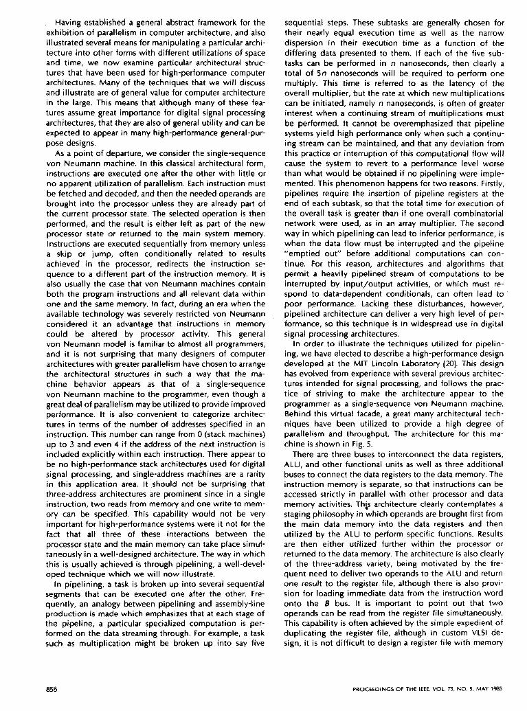
In order to illustrate the techniques utilized for pipelin- ing, we have elected to describe a high-performance design developed at the MIT Lincoln Laboratory [20]. This design has evolved from experience with several previous architec- tures intended for signal processing, and follows the prac- tice of striving to make the architecture appear to the programmer as a single-sequence von Neumann machine. Behind this virtual facade, a great many architectural tech- niques have been utilized to provide a high degree of parallelism and throughput. The architecture for this ma- chine is shown in Fig. 5.
There are three buses to interconnect the data registers, ALU, and other functional units as well as three additional buses to connect the data registers to the data memory. The instruction memory is separate, so that instructions can be accessed strictly in parallel with other processor and data memory activities. This architecture clearly contemplates a staging philosophy in which operands are brought first from the main data memory into the data registers and then utilized by the ALU to perform specific functions. Results are then either utilized further within the processor or returned to the data memory. The architecture is also clearly of the three-address variety, being motivated by the fre- quent need to deliver two operands to the ALU and return one result to the register file, although there is also provi- sion for loading immediate data from the instruction word onto the B bus. It is important to point out that two operands can be read from the register file simultaneously. This capability is often achieved by the simple expedient of duplicating the register file, although in custom VLSl de- sign, it is not difficult to design a register file with memory
858 PROCEEDINGS O F THE IEEE. VOL. 73, NO. 5, M A Y 1985
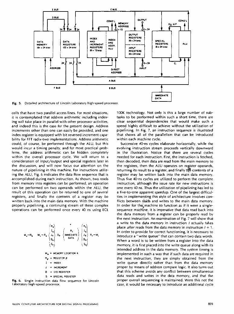
Fig. 5.
E B U S C BUS
k D BUS
COND’L COND’L CIJ. U.P.
r f l 8 I 24 1 t~ I t , I
I I OUTPUT
INDEX I INDEX REGISTERS (8 I 24 bnl DATA
REGISTERS I32 I 24 bml IBk x 24 bnl
ALU REGISTERS -----------. INCREMENT REGISTERS MEMORY AND DATA
181 13bml I REGISTERS
1 AND SPECIAL
(8 # 24 but ALU INPUT
I I 18 I 24 btrl I 1 A
24,’ ,‘24 24,’ I # A I I “ t t C,
ADDRESS DIRECT ADDRESS
INPUT
t v v 7 A 8us
i
F BUS B BUS t IMMEDIATE DATA
Detailed architecture of Lincoln Laboratory high-speed processor.
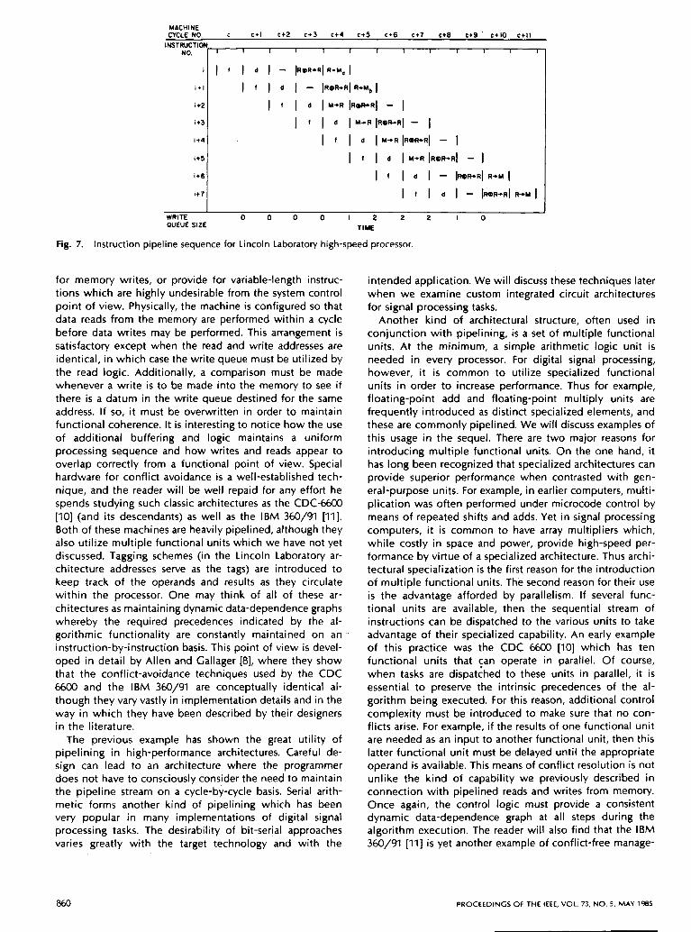
cells that have two parallel access lines. For most situations, it is contemplated that address arithmetic including index- ing will take place in parallel with other processor activities, and indeed this is the case for the present design. Address increments other than one can easily be provided, and one index register is equipped with bit reversed increment capa- bility for FFT radix-two implementations. Address arithmetic could, of course, be performed through the ALU, but this would incur a timing penalty, and for most practical prob- lems, the address arithmetic can be hidden completely within the overall processor cycle. We will return to a consideration of input/output and special registers later in the discussion, and will now focus our attention on the nature of pipelining in this machine. For instructions utiliz- ing the ALU, Fig. 6 indicates the data flow sequence that is accomplished during each instruction. As shown, two reads from memory into registers can be performed, an operation can be performed on two operands within the ALU, the result of this operation can be returned to one of several registers, and finally the contents of a register may be written back into the main data memory. With the machine properly pipelining, a continuing stream of these complex operations can be performed once every 40 ns using ECL
M, = MEMORY LOCATION a
RI = REGISTER B I = INDEX
J = INCREMENT
B = I/O REGISTER
S = SPECIAL REGISTER
Fig. 6. Single instruction data flow sequence for Lincoln Laboratory high-speed processor.
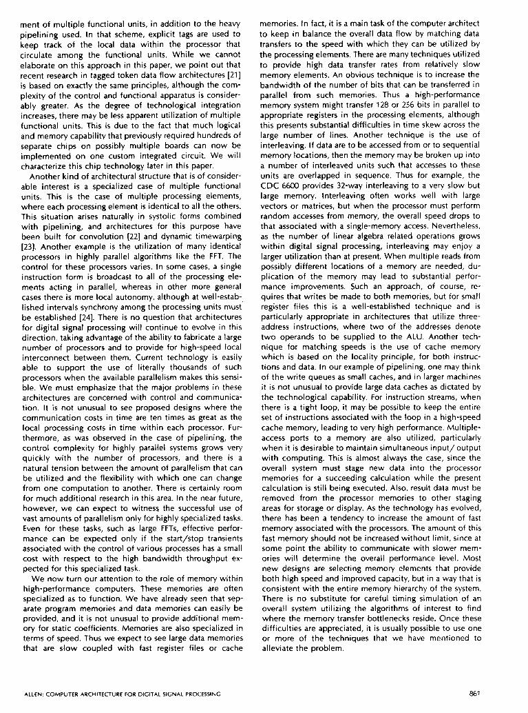
100K technology. Not only is this a large number of sub- tasks to be performed within such a short time, there are clear sequential dependencies that would make such a speed highly difficult to achieve without the utilization of pipehning. In Fig. 7, an instruction sequence is illustrated that shows all of the parallelism that can be introduced within each machine cycle.
Successive 40-ns cycles elaborate horizontally, while the evolving instruction stream proceeds vertically downward in the illustration. Notice that there are several cycles needed for each instruction. First, the instruction is fetched, then decoded, then data are read from the main memory to the registers, then the ALU operates on re ister operands, returning its result to a register, and finally t k contents of a register may be written back into the main data memory. Thus five 40-ns cycles are utilized to perform the complete instruction, although the issue rate for new instructions is one every 40 ns. Thus the utilization of pipelining has led to a five-to-one apparent speedup. One of the largest difficul- ties in implementing this style of architecture involves con- flicts between r&& and writes to the main data memory. In order for thgmachine to function as if i t were a single- sequence mach”!ne, it is imperative that data read back into the data memory from a register can be properly read by the next instruction. An examination of Fig. 7 will show that a write to the data memory in instruction I actually takes place after reads from the data memory in instruction I + 1, In order to provide for correct functioning, it is necessary to introduce a “write queue” that can contain two data words. When a word is to be written from a register into the data memory, it i s first placed into the write queue along with its intended address in the data memory. The system timing is implemented in such a way that i f such data are required in the next instruction, they are simply obtained from the write queue directly rather than from the data memory proper by means of address compare logic. It also turns out that this scheme avoids any conflict between simultaneous data reads and writes in the data memory, and that the proper overall sequencing is maintained. Were this not the case, it would be necessary to introduce an additional cycle
ALLEN COMPUTER ARCHITECTURE F O R DIGITAL SIGNAL PROCESSING 859
for memory writes, or provide for variable-length instruc- tions which are highly undesirable from the system control point of view. Physically, the machine is configured so that data reads from the memory are performed within a cycle before data writes may be performed. This arrangement is satisfactory except when the read and write addresses are identical, in which case the write queue must be utilized by the read logic. Additionally, a comparison must be made whenever a write is to be made into the memory to see if there is a datum in the write queue destined for the same address. If so, i t must be overwritten in order to maintain functional coherence. It is interesting to notice how the use of additional buffering and logic maintains a uniform processing sequence and how writes and reads appear to overlap correctly from a functional point of view. Special hardware for conflict avoidance is a well-established tech- nique, and the reader will be well repaid for any effort he spends studying such classic architectures as the CDC-6600 [IO] (and its descendants) as well as the IBM 360/9l [Ill. Both of these machines are heavily pipelined, although they also utilize multiple functional units which we have not yet discussed. Tagging schemes (in the Lincoln Laboratory ar- chitecture addresses serve as the tags) are introduced to keep track of the operands and results as they circulate within the processor. One may think of all of these ar- chitectures as maintaining dynamic data-dependence graphs whereby the required precedences indicated by the al- gorithmic functionality are constantly maintained on an instruction-by-instruction basis. This point of view is devel- oped in detail by Allen and Gallager [8], where they show that the conflict-avoidance techniques used by the CDC 6600 and the IBM 360/9l are conceptually identical al- though they vary vastly in implementation details and in the way in which they have been described by their designers in the literature.
The previous example has shown the great utility of pipelining in high-performance architectures. Careful de- sign can lead to an architecture where the programmer does not have to consciously consider the need to maintain the pipeline stream on a cycle-by-cycle basis. Serial arith- metic forms another kind of pipelining which has been very popular in many implementations of digital signal processing tasks. The desirability of bit-serial approaches varies greatly with the target technology and with the
intended application. We will discuss these techniques later when we examine custom integrated circuit architectures for signal processing tasks.
Another kind of architectural structure, often used in conjunction with pipelining, is a set of multiple functional units. At the minimum, a simple arithmetic logic unit is needed in every processor. For digital signal processing, however, it i s common to utilize specialized functional units in order to increase performance. Thus for example, floating-point add and floating-point multiply units are frequently introduced as distinct specialized elements, and these are commonly pipelined. We will discuss examples of this usage in the sequel. There are two major reasons for introducing multiple functional units. On the one hand, it has long been recognized that specialized architectures can provide superior performance when contrasted with gen- eral-purpose units. For example, in earlier computers, multi- plication was often performed under microcode control by means of repeated shifts and adds. Yet in signal processing computers, it is common to have array multipliers which, while costly in space and power, provide high-speed per- formance by virtue of a specialized architecture. Thus archi- tectural specialization is the first reason for the introduction of multiple functional units. The second reason for their use is the advantage afforded by parallelism. If several func- tional units are available, then the sequential stream of instructions can be dispatched to the various units to take advantage of their specialized capability. An early example of this practice was the CDC 6600 [IO] which has ten functional units that can operate in parallel. Of course, when tasks are dispatched to these units in parallel, it is essential to preserve the intrinsic precedences of the al- gorithm being executed. For this reason, additional control complexity must be introduced to make sure that no con- flicts arise. For example, if the results of one functional unit are needed as an input to another functional unit, then this latter functional unit must be delayed until the appropriate operand is available. This means of conflict resolution is not unlike the kind of capability we previously described in connection with pipelined reads and writes from memory. Once again, the control logic must provide a consistent dynamic data-dependence graph at all steps during the algorithm execution. The reader will also find that the IBM 360/9 [Ill is yet another example of conflict-free manage-
860 PROCEEDINGS O F THE IEEE, VOL. 73, NO. 5 , M A Y 1985
ment of multiple functional units, in addition to the heavy pipelining used. In that scheme, explicit tags are used to keep track of the local data within the processor that circulate among the functional units. While we cannot elaborate on this approach in this paper, we point out that recent research in tagged token data flow architectures [21] is based on exactly the same principles, although the com- plexity of the control and functional apparatus is consider- ably greater. As the degree of technological integration increases, there may be less apparent utilization of multiple functional units. This is due to the fact that much logical and memory capability that previously required hundreds of separate chips on possibly multiple boards can now be implemented on one custom integrated circuit. We will characterize this chip technology later in this paper.
Another kind of architectural structure that is of consider- able interest is a specialized case of multiple functional units. This is the case of multiple processing elements, where each processing element is identical to all the others. This situation arises naturally in systolic forms combined with pipelining, and architectures for this purpose have been built for convolution [22] and dynamic timewarping [23]. Another example is the utilization of many identical processors in highly parallel algorithms like the FFT. The control for these processors varies. In some cases, a single instruction form is broadcast to all of the processing ele- ments acting in parallel, whereas in other more general cases there i s more local autonomy, although at well-estab- lished intervals synchrony among the processing units must be established [24]. There is no question that architectures for digital signal processing will continue to evolve in this direction, taking advantage of the ability to fabricate a large number of processors and to provide for high-speed local interconnect between them. Current technology is easily able to support the use of literally thousands of such processors when the available parallelism makes this sensi- ble. We must emphasize that the major problems in these architectures are concerned with control and communica- tion. It i s not unusual to see proposed designs where the communication costs in time are ten times as great as the local processing costs in time within each processor. Fur- thermore, as was observed in the case of pipelining, the control complexity for highly parallel systems grows very quickly with the number of processors, and there is a natural tension between the amount of parallelism that can be utilized and the flexibility with which one can change from one computation to another. There is certainly room for much additional research in this area. In the near future, however, we can expect to witness the successful use of vast amounts of parallelism only for highly specialized tasks. Even for these tasks, such as large FFTs, effective perfor- mance can be expected only if the start/stop transients associated with the control of various processes has a small cost with respect to the high bandwidth throughput ex- pected for this specialized task.
We now turn our attention to the role of memory within high-performance computers. These memories are often specialized as to function. We have already seen that sep- arate program memories and data memories can easily be provided, and it is not unusual to provide additional mem- ory for static coefficients. Memories are also specialized in terms of speed. Thus we expect to see large data memories that are slow coupled with fast register files or cache
memories. In fact, it is a main task of the computer architect to keep in balance the overall data flow by matching data transfers to the speed with which they can be utilized by the processing elements. There are many techniques utilized to provide high data transfer rates from relatively slow memory elements. An obvious technique is to increase the bandwidth of the number of bits that can be transferred in parallel from such memories. Thus a high-performance memory system might transfer 128 or 256 bits in parallel to appropriate registers in the processing elements, although this presents substantial difficulties in time skew across the large number of lines. Another technique is the use of interleaving. If data are to be accessed from or to sequential memory locations, then the memory may be broken up into a number of interleaved units such that accesses to these units are overlapped in sequence. Thus for example, the CDC 6600 provides 32-way interleaving to a very slow but large memory. Interleaving often works well with large vectors or matrices, but when the processor must perform random accesses from memory, the overall speed drops to that associated with a single-memory access. Nevertheless, as the number of linear algebra related operations grows within digital signal processing, interleaving may enjoy a larger utilization than at present. When multiple reads from possibly different locations of a memory are needed, du- plication of the memory may lead to substantial perfor- mance improvements. Such an approach, of course, re- quires that writes be made to both memories, but for small register files this is a well-established technique and is particularly appropriate in architectures that utilize three- address instructions, where two of the addresses denote two operands to be supplied to the ALU. Another tech- nique for matching speeds is the use of cache memory which is based on the locality principle, for both instruc- tions and data. In our example of pipelining, one may think of the write queues as small caches, and in larger machines it i s not unusual to provide large data caches as dictated by the technological capability. For instruction streams, when there i s a tight loop, it may be possible to keep the entire set of instructions associated with the loop in a high-speed cache memory, leading to very high performance. Multiple- access ports to a memory are also utilized, particularly when it is desirable to maintain simultaneous input/ output with computing. This is almost always the case, since the overall system must stage new data into the processor memories for a succeeding calculation while the present calculation is still being executed. Also, result data must be removed from the processor memories to other staging areas for storage or display. As the technology has evolved, there has been a tendency to increase the amount of fast memory associated with the processors. The amount of this fast memory should not be increased without limit, since at some point the ability to communicate with slower mem- ories will determine the overall performance level. Most new designs are selecting memory elements that provide both high speed and improved capacity, but in a way that is consistent with the entire memory hierarchy of the system. There is no substitute for careful timing simulation of an overall system utilizing the algorithms of interest to find where the memory transfer bottlenecks reside. Once these difficulties are appreciated, it i s usually possible to use one or more of the techniques that we have mentioned to alleviate the problem.
ALLEN: COMPUTER ARCHITECTURE F O R DIGITAL SIGNAL PROCESSING 861
In our earlier mention of multiple processing elements, our focus was directed to those processors acting directly on data as part of the algorithmic execution. All high-per- formance systems, however, require additional processors for control. We have already seen that the processing needed to maintain conflict-free operation and to balance data flow through the several memories of a system can be substantial. The greater the degree of parallelism, and the possibility for introducing dynamic data-dependence capa- bility, the more control complexity can be expected. Fur- thermore, control processors are necessary to perform ad- dress generation and for decision making resulting from data-dependent conditionals and hardware or software malfunction. What is clear is that modern high-performance architectures, particularly those providing several tens of megaflops speed, require several different levels of control that must be coordinated through a separate processor. While earlier machines often provided this control directly in terms of random logic, it is much more common to see this control embedded in a well-recognized processor that runs part or all of the computer operating system. Contem- porary microprocessors are often used for this purpose, as they provide adequate speed and performance without the necessity to design special-purpose logic for each computer system that is designed. Clearly these control processors can execute in parallel with other elements, and unlike the data flow processors, they utilize very little pipelining in order to retain a degree of flexibility to respond to a variety of interrupt situations.
The last kind of architectural structure that must be mentioned concerns input/output. Here, of course, we must be concerned with not only the amount of data to be transferred, but also the speed of the transfers. In some architectures, for overall throughput reasons it is common to transfer an entire block of data to the specialized processor and then return the results as a block later to the host processor. On the other hand, relatively low-speed plug-in boards that are used to enhance particular calcula- tions, such as FFT, often use a direct memory access con- nection so there is no block transfer of data from the host computer to any processor memory. This approach obvi- ously cuts down the need for such memory in the processor, and makes sense when the data can be accessed from or to the host machine at speeds that are well matched to the attached processor. Large systems for digital signal processing computing often have several input/output processors associated with them, and although in the past these were often a single physical processor time multi- plexed to provide several virtual processors, at present the technology permits the provision of several separate physi- cal processors for input/output. There are several other interesting aspects of architectural style having to do with input/output. One has to do with the particular instruc- tions utilized in the processor for input/output. In older practice, it was common to have specialized instructions for input/output, yet in recent practice there has been a tend- ency to provide specialized registers for the control of input/output that reside within the normal address space of the processor. In this way, 1/0 operations can be con- trolled and monitored through utilization of the standard instruction set of the machine. Another important aspect of architectural style has to do with the use of flags versus interrupts. When an interrupt is received, at least a partial
state save is necessitated, and in a complicated highly pipelined machine, the amount of control needed for re- sponding to an interrupt may be very high indeed. For this reason, in large complicated machines no interrupts have been provided, so that the program must be carefully for- mulated to inspect flags under program control at ap- propriate intervals. It seems clear that programmers would prefer to deal with interrupts, since there is a well-estab- lished software methodology for their utilization and also because any machine that provides interrupts almost inevi- tably provides program flags when they are desirable. It is usually the computer architect and the digital designer that prefer the use of program flags to interrupts, due to the control complexity introduced in highly parallel pipelined machines. Nevertheless, as control becomes more regu- larized through utilization of programmed control proc- essors, interrupts are becoming more predominant in newer designs.
From the discussion above it is apparent that an aggres- sive architecture for digital signal processing may provide a large variety of architectural structures to enhance perfor- mance. These will range through pipelining and special hardware for conflict avoidance, through multiple func- tional units and specialized processing elements coupled with a well developed memory hierarchy that can support continued high-speed computation over a broad class of algorithms. Processors and memories are often duplicated in order to provide speed, and specialized processors are introduced for address calculations, generalized control, and input/output. High-performance computer systems for digital signal processing-utilize all of these techniques cou- pled with aggressive technology. They provide, as we shall see, a literal tour de force of architectural techniques, and since we have noted the increasing complexity of the tasks undertaken in digital signal processing, we can expect the industry in this field to continue to exploit all possible architectural and technological techniques for high-speed performance.
IV. TECHNOLOGY
Of all the factors that influence computer architecture, technology i s without question the most important. It is not difficult to show how important architectural ideas, such as general register files, became significant only when the appropriate enabling technology was available, and that other ideas, such as multiple specialized processors took on reduced implementations through techniques such as time multiplexing until the technology made completely distinct multiple processors economically viable. Not only i s tech- nology an incredibly important factor in the determination of architectures, it is an exceedingly robust and volatile area. it is probably impossible to overemphasize how fast technology is changing, so that in a very real sense, any commercially available machine is technologically obsolete. For example, in the memory area the number of bits per integrated circuit is increasing at a rate of 70 percent per year, and the logic density available (number of gates per unit area) is increasing by 25 percent per year. The area of individual integrated circuit die is increasing by 20 per- cent per year, and the power delay product associated with contemporary processes is dropping by a factor of two each year. The main negative factor associated with this rapid
862 PROCEEDINGS O F THE IEEE, VOL. 73, NO. 5 , M A Y 1985
growth in technology is that the cost of design has been rising by at least 40 percent a year, and we will address this factor later in this section.
The factors that need to be addressed with respect to technology include size, speed, power, heat dissipation, packaging, and input/output capability. At the circuit level, IC technology can be grouped by device type and circuit design style. Device types include bipolar and unipolar transistors, as well as Josephson Junction devices. Bipolar transistors are utilized in the ubiquitous TTL technology, as well as emitter-coupled logic, the latter being the highest speed circuit style in general use within computer systems. Unipolar devices are more commonly referred to as MOS transistors, and these are available both as p-channel de- vices (PMOS) and n-channel devices (NMOS), or combined together in a low-power circuit style called CMOS. TTL circuits provide gate delays of 2-5 ns, together with modest power dissipation. For all but the highest speed applica- tions, these circuits are in common use, and it is possible to obtain substantial logical or register memory capability on such a chip. When all-out speed is required, there is no substitute for emitter-coupled logic, and several important signal processing machines utilize either the 10K or faster 100K series ECL circuits. While these circuits are very fast, the density of integration on each chip is not as high as for TTL, and the attendant power dissipation can rise to several watts per chip, leading to special cooling needs. Among the MOS circuit styles, NMOS provides the densest and fastest circuits, but often involves static power dissipation that can limit the amount of circuitry on an individual chip. All contemporary large dynamic RAM memories are NMOS, and most high-end microprocessors are currently made in NMOS technology. Due to many advances in processing, however, CMOS is growing rapidly due to its low power dissipation, coupled with increasing density and speed. Increasingly, signal processing chips such as multipliers and general-purpose signal processors are being implemented in CMOS technology. With CMOS, it is now possible to achieve gate delays of less than 2 ns and large (64K) static RAMS are currently available in CMOS.
In addition to the device type and circuit style, it is important t o consider the design style associated with different technologies. Most engineers are familiar with off-the-shelf small-scale and medium-scale integration components, but semi-custom and full-custom techniques for design are becoming increasingly popular. For example, gate arrays provide very fast design turnaround together with low risk and substantial performance improvements in many cases. Gate arrays are available in TTL, ECL, and CMOS technologies, and up to IOOOO gates can be placed on a CMOS array while up to 3500 gates can be placed on an ECL array. Both of these figures can be expected to grow rapidly in the near future. Standard cell capability provides even greater density than gate arrays, and hence &eater functionality per chip, through a higher degree of customi- zation within each functional cell on the chip. The cost and risk of this approach is higher than for gate arrays, and the turnaround time is longer, but it provides performance that begins to approximate that found in a good custom design. Finally, there is full-custom design. The phrase ”full custom” needs careful interpretation, since many will imagine that each and every transistor on a full-custom design must be individually specified by the design engineer. Since there
are custom chips in production containing over 500000 transistors, this is clearly an impossible task, and indeed, a number of powerful techniques are used to cut down the design effort while providing the advantages of fully custo- mized circuitry. In the digital signal processing area, per- haps the most interesting development has been the recent appearance of specialized function generators for those complex cells that are frequently used in signal processing. For some time it has been common to utilize program logic array generators, and these useful programs can be thought of as specialized silicon compilers transforming an input functional logic specification into a target layout architec- ture of a very prescribed sort. Borrowing from this idea, specialized compilers, each with its own highly optimized target layout architecture, have recently been developed. For example, specialized multiplier compilers now exist [25] that convert two integers, namely the length of the desired multiplier and multiplicand, to a complete layout using an array of carry/save adders together with modified Booth’s recoding. Such a layout is highly regular and is very close in efficiency to that obtainable by an optimized manual de- sign. Shortly such techniques will be extended to floating- point units, so that the designer can merely specify the floating-point function (e.g., multiplication or addition) to- gether with the size of the exponent and the size of the mantissa desired, and obtain the final layout of a highly optimized cell for this purpose. These techniques fit into an overall perspective on design whereby the user initially specifies a high-level functional specification of the overall chip, which is then compiled into a fully parallel data-de- pendence graph. An exploration phase follows, such as we have described earlier in this paper, to pick out the degree of parallelism appropriate for the designer’s intentions. The result of this phase will be a block diagram containing components which must then be realized by the kinds of silicon compilation processes that we have been discussing here. In this way, the overall chip is not obtained through a single compilation process, but instead the design engineer guides the overall process to a level where expert function generators can produce the large amount of layout detail needed for the finished chip. Of course, placement and routing capability [26] must also be coupled to this strategy in order to produce a final design. From this view, it should be clear that modern “full-custom” integrated circuit de- sign does not involve the substantial penalties in time and effort required by earlier custom design techniques. In effect, the experience of expert designers is being encapsu- lated into procedural forms of knowledge representation that can generate specific forms of these circuits upon demand. This means that specialized signal processing chips with a high degree of performance can now be generated much more easily than heretofore. It is also important to emphasize the use of high-level compilation and proce- dural techniques in the assembly of pre-existing compo- nents on a chip. For example, Denyer [27] has recently introduced a compiler for signal processing tasks utilizing serial arithmetic and NMOS technology. Designers with little integrated circuit design experience have found it possible to design filters and FFT modules utilizing this compiler in a few weeks time. The compiler assembles the needed modules, places them, and routes them all to- gether, while providing simulation capability to provide assurance that the resulting circuit provides the intended
ALLEN. COMPUTER ARCHITECTURE FOR DIGITAL SIGNAL PROCESSING 863
functionality. The resulting layouts are not highly optimal, but they are indeed very useful, and in the next few years we can expect to see continued development and optimiza- tion of these techniques.
No discussion of technology for digital signal processing would be complete without a mention of contemporary performance for the most important canonical circuit forms. Certainly that task which has received the most design attention is multiplication [28], and it can be viewed as providing a tour de force of architectural space/time trade- offs. Multiplication can be regarded algorithmically as con- sisting of repeated shifts and adds of the multiplicand as specified by the bits of the multiplier, and this technique is frequently implemented. On the other hand, there are a wide variety of other techniques, including avoidance of multiplication, which are frequently used. In filter imple- mentations where the coefficients are fixed, it is sometimes worthwhile to merely provide for the required additions within a multiplication, particularly when the number of ones in the coefficient multiplier is relatively small. Tech- niques have been introduced for reducing the number of such specified additions within a multiplier subject to the functional specification of the filter containing the multipli- cation, and many signal processing chips, including those utilized for finite impulse response filters, provide for no explicit multiplication. When more general capability is required, however, a complete two’s complement multi- plier is generally provided, using either serial arithmetic or parallel arithmetic. For some time there has been a raging debate as to the goodness of serial versus parallel ap- proaches. Advocates of the serial approach cite the small area required, interconnect simplicity, high throughput, and low power dissipation. On the other hand, critics mention the difficulty of performing data-dependent conditional operations in serial arithmetic which is inherently very deeply pipelined, and ascribe high importance to the inter- connect problem only when such lines must go off-chip. Certainly there are many chips available with wide busses on-chip, and these do not consume an excessive area in most applications. Parallel multipliers are preferred by those desiring high speed with minimum latency in throughput. While serial techniques have undoubtedly proved to be very useful in many applications, improvements in technol- ogy and circuit design are leading to very fast and dense parallel multipliers, which will occupy only a very small fraction of a chip. While contemporary designs provide for 16 X 16 NMOS multipliers operating in well under 200 ns, new results can be expected shortly that provide this same functional capability in approximately 50 ns. Not only will the speed be obtained, but the capability will be provided in low-power CMOS technology. This is a highly competi- tive business with several manufacturers continuing to pro- vide highly aggressive offerings. It is perhaps well to mention here the possible use of gallium arsenide as integrated circuit material rather than silicon. Here again, a huge debate arises over the virtues of gallium arsenide as op- posed to silicon. It is our belief that silicon will continue to dominate in a major way although impressive laboratory results with gallium arsenide have been measured. For example, a gallium arsenide 16 X 16 multiplier operating in 11 ns has recently been reported [29], and designs are underway to achieve 32 X 32-bit multiplication in gallium arsenide within 1 5 ns. These are indeed very impressive times, although it must be emphasized that they are not
commercially available, and probably cannot be expected within the next five years.
We turn now to packaging. This is an exceedingly im- portant area, and it is probably not an overstatement to say that as much technological innovation has gone into packaging in recent years as into device and circuit design. As the amount of circuitry increases on a chip, the need for input/output circuitry rises accordingly, so that the need for new packages with large numbers of pins has been increasingly felt. Without question, the most impressive technology in this area has been developed by IBM through a combination of its introduction of “solder ball” technol- ogy with multilevel ceramic substrates [30]. In conventional integrated circuits, connections are made from the chip to the package through bonding pads around the periphery of the chip. In the IBM approach, however, pads can be provided anywhere on the chip, and connections are made to the package by means of very small solder balls, thus making for a much more flexible and dependable input/output capability from the chip to. the package. This interconnection strategy is then coupled with up to 33 levels of interconnect between ceramic layers, where the conductors are provided by thick-film paste. When one remembers that the speed of light in air is approximately 1 ns/ft, and that contemporary ECL gate delays are of the order of 350 ps, it is easy to see why such packaging technology is so important. It also turns out that this tech- nology is fairly easy to adapt for cooling purposes, since the entire bottom of the chip is available for contact with heat-exchanger materials. Signal processing machines are now beginning to appear with ECL gate arrays dissipating approximately 4 W [31] that require carefully designed forced air cooling, so that these packaging considerations will become increasingly important in the years ahead. It is also important to mention here that the engineering design of large high-performance digital signal processing systems requires large capabilities in simulation and verification. Not only is logic simulation required, but very careful timing verification must be provided which takes into account the characterization of the packaging. Design software is also available for dealing with cooling require- ments, even to the extent of pinpointing hot spots on projected chip designs. The thrust of many of our com- ments here has been to show that the design of large high-performance digital signal processing systems can no longer be regarded as a manual exercise guided by the accumulated skill of the engineer. The reason is that the level of complexity is simply too large for this previously utilized design style. Complexity of functionality and design has forced designers to think carefully about the represen- tational levels that are important to control in design, and to provide simulation and verification tools appropriate to these concerns. This is now an active area of research, and one where new advances are appearing at frequent inter- vals.
Another general trend that is important to note is the increasing utilization of hybrid techniques in both technol- ogy and circuit types. In previous years, we have been accustomed to seeing restricted classes of circuits imple- mented in one technology made available, such as arith- metic logic unit capability and T T L technology. As the amount of capability provided by a given chip increases, these distinctions are blurring both as to technology and circuit function. For example, aggressive new processes
864 PROCEEDINGS OF THE IEEE, VOL. 73, NO. 5, M A Y 1985
provide NMOS, CMOS, and limited bipolar capability all in the same process on the same chip. Thus on a large static RAM specialized NMOS circuits can be used for high den- sity and high speed in the interior of the array, and yet all peripheral decoding and access circuitry can utilize low- power CMOS together with bipolar capability for driving the pads. Furthermore, logic and memory are being merged together in many designs. This is certainly seen in the contemporary signal processing chips, but even in gate arrays, the trend is to include logic and memory together, rather than forcing the user to build memory modules in an inefficient manner from the previously furnished gates. These trends are, of course, yet another example of the optimization of the technology in the direction of the intended functionality. This movement calls for an increase in process complexity along with circuit variation and flexi- bility, as well as design techniques that can efficiently utilize these resources. It is all part of a picture of increas- ingly sophisticated technology being carefully tuned to the needs of end users.
We turn now to the consideration of specialized signal processing chips. A number of these are currently available commercially, and many more can be expected in the future. Rather than attempt to give a survey of all of these parts, we instead pick one design, the Texas Instruments TMS32010 [32] which is widely utilized in many applica- tions. This part is fabricated in NMOS technology (although it is currently being redesigned into CMOS) and operates with a 200-ns instruction cycle time. Sixteen-bit instruction and data words are utilized, together with a 32-bit ALU/ac- cumulator. A 16 X 16 multiplication takes place within the 200-ns cycle time, and a 0-15-bit barrel shifter is provided. Two hundred and eighty-eight bytes of on-chip data RAM are provided, although this can be expanded externally to a total of 8K bytes at full speed. In one version, 3K bytes of on-chip program ROM are also provided. Eight input and eight output channels are available, together with a 16-bit bidirectional data bus with 40-Mbit/s transfer rate. The die size is approximately 49000 mils2, the power dissipation 1 W, and the standard package is a 40-pin dual in-line package. The reader is referred to the literature [32] for a comprehen- sive discussion of this design, but Fig. 8 shows the architec- tural block diagram, and Fig. 9 shows a micro-photograph of the chip. The block diagram is fairly straightforward, each component being labeled functionally. The use of a multi- plier, together with shifter and accumulator to produce sums of products, together with a possibility of an output shift is a highly useful and general capability. Separate program and data memories are provided, and a variety of addressing modes including direct addressing, indirect ad- dressing, and immediate addressing are provided on the chip. For filtering and FFT applications, the inclusion of a multiply immediate instruction is very useful since it both saves on data storage for the coefficients, but also saves their access time. It is clear what the direction of continuing evolution of such chips will be. Without question, given the capability to place over half a million transistors at 1-pm Iinewidths on a single die, users will want and receive large amounts of on-chip program and data memory. This is probably the most pressing current requirement. As the technology heads in the direction of providing, for exam- ple, I - p m CMOS capability, speed improvements will also be available, with previously cited 16 X 16 multiplier speeds of well below 50 ns coupled with processor cycle times in
the neighborhood of 25 ns. The kind of highly overlapped pipelined architecture previously described in this paper will become readily available in the next five years on a single chip, leading to extremely aggressive performance. In fact, such single-chip systems will be so complex, that a major part of the development cost is the construction of development software, including not only conventional simulators and compilers, but real-time simulation, verifica- tion, and testing capability within the context of larger systems. The provision of such capability is a tall order, and we can expect to see that the number of specialized digital signal processing chips of high complexity will go down due to the sheer magnitude of the design and support effort required. The capability of these chips will be SO
large, both in terms of hardware and software, that it will be practical for many applications to fit onto these chips without the need for specialized or custom hardware. In- deed, the chips that we have foreseen here will compete aggressively with current board level products from a num- ber of manufacturers.
We leave our discussion of technology with a view of some new directions i n highly integrated system architec- tures that are currently becoming available. We have al- ready noted that chips are becoming larger and larger, to the extent that we can expect chips 1 in on a side by the year 1990. There is thus a natural tendency to think of placing entire systems, including processing and memory and input/output capability all within one chip. As the size of the chip grows, however, the yield for a given level of technology goes down, so that at any given time very large chips are not economically viable. One attempt to avert these difficulties is to utilize wafer-scale integration, wherein an entire system is built on a wafer using re- dundancy and discretionary interconnect techniques. The overall system is divided up into a number of modules, which are placed, using a redundancy factor of perhaps two, over a regular grid on a wafer. After the wafer has been fabricated, all of the modules are individually tested while the wafer is still intact. Those modules that are found to function satisfactorily are then connected to the overall interconnect network which utilizes thick metal lines, using laser [33] or electron-beam techniques [34] which are cur- rently well understood. In this way, a high-performance system fabricated utilizing a highly disciplined interconnect technology can be achieved within a very small space. Recent examples of designs in this framework include a fully parallel 16-point FFT [3], using serial arithmetic. In this design, all 32 butterflies are physically implemented, to- gether with a redundancy factor of two, so that no fewer than 32 X 2 X 4 = 256 serial multipliers are provided on the wafer. This design is also accompanied by high band- width input and output capability commensurate with this level of arithmetic capability. In another example, a systolic design for dynamic timewarping has been specified for wafer scale design [35]. Once again, a highly regular archi- tecture is found to be suitable for the wafer scale tech- nology, and can provide a high level of performance.
V. PROGRAMMING
For many years, the emphasis in digital signal processing has been on speed, and most users have worked hard to make every bit count. For this reason, many of the older
ALLEN: COMPUTER ARCHITECTURE F O R DIGITAL SIGNAL PROCESSING 865
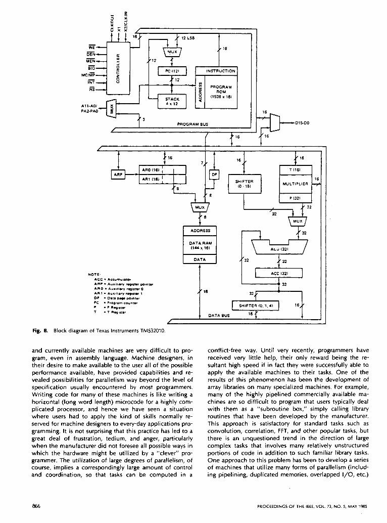
I I 16
AR01161 1 A R l (161 I
.
4’ 8
fig. 8. Block diagram of Texas Instruments TMS32010.
‘-& i SHIFTER 10. 151
DATA RAM 1144 1161
I DATA I
I l 6
;
T 1161
MULTIPLIER
P 1321
12 MUX
E27 ALU 1321
SHIFTER IO. 1.41
1 DATA BUS
and currently available machines are very difficult to pro- gram, even in assembly language. Machine designers, in their desire to make available to the user all of the possible performance available, have provided capabilities and re- vealed possibilities for parallelism way beyond the level of specification usually encountered by most programmers. Writing code for many of these machines is like writing a horizontal (long word length) microcode for a highly com- plicated processor, and hence we have seen a situation where users had to apply the kind of skills normally re- served for machine designers to every-day applications pro- gramming. It is not surprising that this practice has led to a great deal of frustration, tedium, and anger, particularly when the manufacturer did not foresee all possible ways in which the hardware might be utilized by a “clever” pro- grammer. The utilization of large degrees of parallelism, of course, implies a correspondingly large amount of control and coordination, so that tasks can be computed in a
conflict-free way. Until very recently, programmers have received very little help, their only reward being the re- sultant high speed if in fact they were successfully able to apply the available machines to their tasks. One of the results of this phenomenon has been the development of array libraries on many specialized machines. For example, many of the highly pipelined commercially available ma- chines are so difficult to program that users typically deal with them as a “subroutine box,” simply calling library routines that have been developed by the manufacturer. This approach is satisfactory for standard tasks such as convolution, correlation, FFT, and other popular tasks, but there is an unquestioned trend in the direction of large complex tasks that involves many relatively unstructured portions of code in addition to such familiar library tasks. One approach to this problem has been to develop a series of machines that utilize many forms of parallelism (includ- ing pipelining, duplicated memories, overlapped I/O, etc.)
866 PROCEEDINGS OF THE IEEE, VOL. 73, N O . 5, M A Y 1985
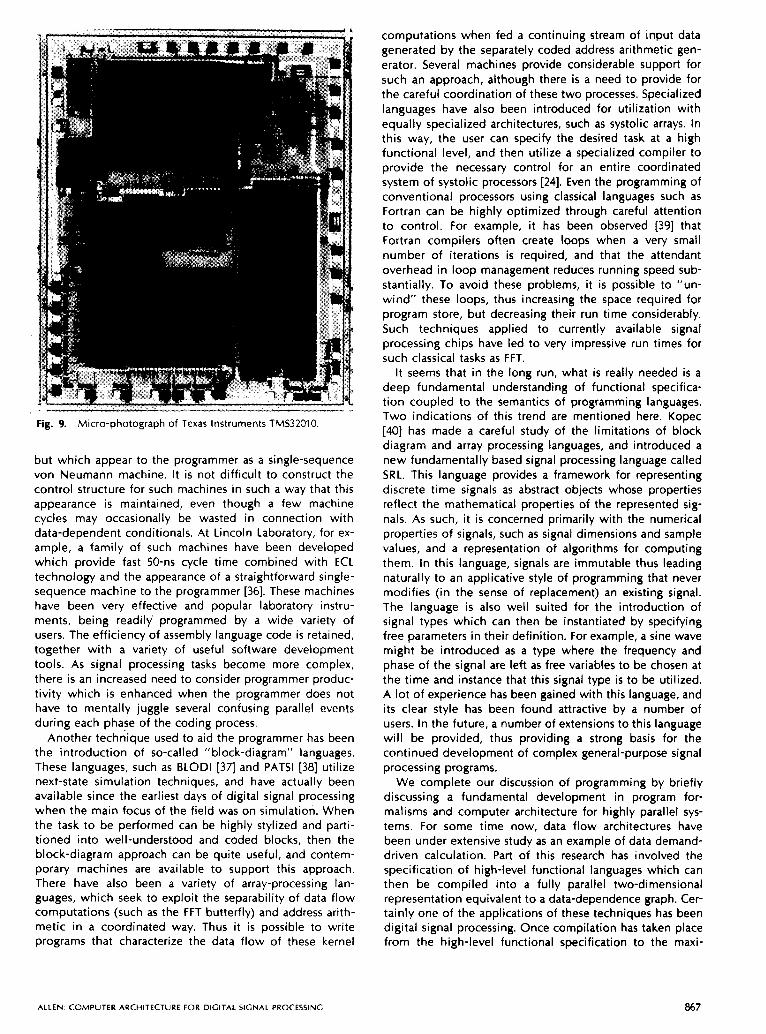
but which appear to the programmer as a single-sequence von Neumann machine. It is not difficult to construct the control structure for such machines in such a way that this appearance is maintained, even though a few machine cycles may occasionally be wasted in connection with data-dependent conditionals. At Lincoln Laboratory, for ex- ample, a family of such machines have been developed which provide fast 50-ns cycle time combined with ECL technology and the appearance of a straightforward single- sequence machine to the programmer [36]. These machines have been very effective and popular laboratory instru- ments, being readily programmed by a wide variety of users. The efficiency of assembly language code is retained, together with a variety of useful software development tools. As signal processing tasks become more complex, there is an increased need to consider programmer produc- tivity which is enhanced when the programmer does not have to mentally juggle several confusing parallel events during each phase of the coding process.
Another technique used to aid the programmer has been the introduction of so-called “block-diagram” languages. These languages, such as BLODl [37] and PATS1 (381 utilize next-state simulation techniques, and have actually been available since the earliest days of digital signal processing when the main focus of the field was on simulation. When the task to be performed can be highly stylized and parti- tioned into well-understood and coded blocks, then the block-diagram approach can be quite useful, and contem- porary machines are available to support this approach. There have also been a variety of array-processing lan- guages, which seek to exploit the separability of data flow computations (such as the FFT butterfly) and address arith- metic in a coordinated way. Thus it is possible to write programs that characterize the data flow of these kernel
computations when fed a continuing stream of input data generated by the separately coded address arithmetic gen- erator. Several machines provide considerable support for such an approach, although there is a need to provide for the careful coordination of these two processes. Specialized languages have also been introduced for utilization with equally specialized architectures, such as systolic arrays. In this way, the user can specify the desired task at a high functional level, and then utilize a specialized compiler to provide the necessary control for an entire coordinated system of systolic processors [24]. Even the programming of conventional processors using classical languages such as Fortran can be highly optimized through careful attention to control. For example, it has been observed [39] that Fortran compilers often create loops when a very small number of iterations is required, and that the attendant overhead in loop management reduces running speed sub- stantially. To avoid these problems, it is possible to “un- wind” these loops, thus increasing the space required for program store, but decreasing their run time considerably. Such techniques applied to currently available signal processing chips have led to very impressive run times for such classical tasks as FFT.
It seems that in the long run, what is really needed is a deep fundamental understanding of functional specifica- tion coupled to the semantics of programming languages. Two indications of this trend are mentioned here. Kopec [40] has made a careful study of the limitations of block diagram and array processing languages, and introduced a new fundamentally based signal processing language called SRL. This language provides a framework for representing discrete time signals as abstract objects whose properties reflect the mathematical properties of the represented sig- nals. As such, it is concerned primarily with the numerical properties of signals, such as signal dimensions and sample values, and a representation of algorithms for computing them. In this language, signals are immutable thus leading naturally to an applicative style of programming that never modifies (in the sense of replacement) an existing signal. The language is also well suited for the introduction of signal types which can then be instantiated by specifying free parameters in their definition. For example, a sine wave might be introduced as a type where the frequency and phase of the signal are left as free variables to be chosen at the time and instance that this signal type is to be utilized. A lot of experience has been gained with this language, and i ts clear style has been found attractive by a number of users. In the future, a number of extensions to this language will be provided, thus providing a strong basis for the continued development of complex general-purpose signal processing programs.
We complete our discussion of programming by briefly discussing a fundamental development in program for- malisms and computer architecture for highly parallel sys- tems. For some time now, data flow architectures have been under extensive study as an example of data demand- driven calculation. Part of this research has involved the specification of high-level functional languages which can then be compiled into a fully parallel two-dimensional representation equivalent to a data-dependence graph. Cer- tainly one of the applications of these techniques has been digital signal processing. Once compilation has taken place from the high-level functional specification to the maxi-
ALLEN: COMPUTER ARCHITECTURE F O R DIGITAL SIGNAL PROCESSING 867
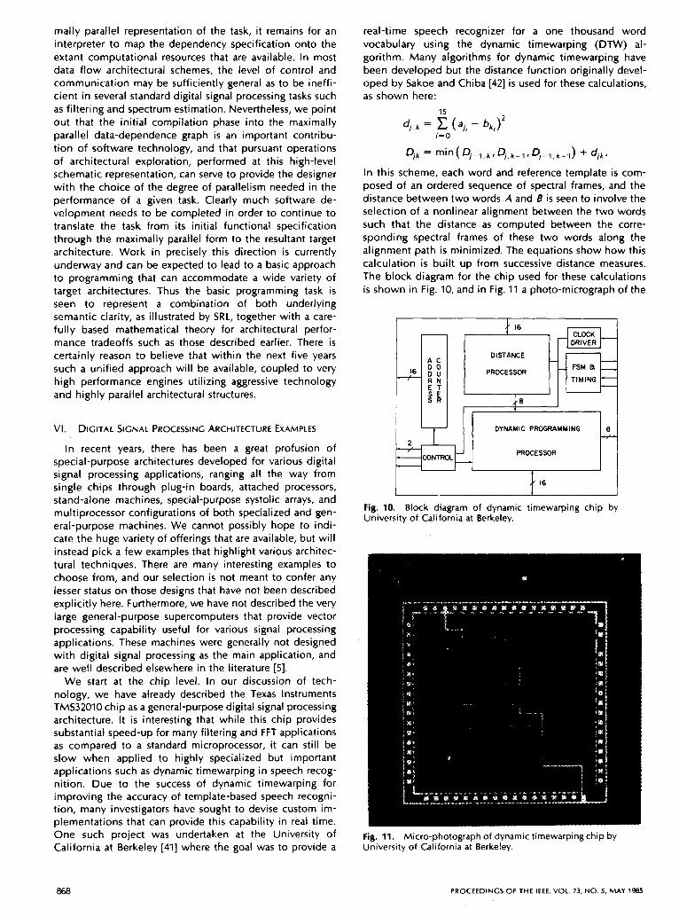
mally parallel representation of the task, it remains for an interpreter to map the dependency specification onto the extant computational resources that are available. In most data flow architectural schemes, the level of control and communication may be sufficiently general as to be ineffi- cient in several standard digital signal processing tasks such as filtering and spectrum estimation. Nevertheless, we point out that the initial compilation phase into the maximally parallel data-dependence graph is an important contribu- tion of software technology, and that pursuant operations of architectural exploration, performed at this high-level schematic representation, can serve to provide the designer with the choice of the degree of parallelism needed in the performance of a given task. Clearly much software de- velopment needs to be completed in order to continue to translate the task from its initial functional specification through the maximally parallel form to the resultant target architecture. Work in precisely this direction is currently underway and can be expected to lead to a basic approach to programming that can accommodate a wide variety of target architectures. Thus the basic programming task is seen to represent a combination of both underlying semantic clarity, as illustrated by SRL, together with a care- fully based mathematical theory for architectural perfor- mance tradeoffs such as those described earlier. There is certainly reason to believe that within the next five years such a unified approach will be available, coupled to very high performance engines utilizing aggressive technology and highly parallel architectural structures.
VI. DIGITAL SIGNAL PROCESSING ARCHITECTURE EXAMPLES
In recent years, there has been a great profusion of special-purpose architectures developed for various digital signal processing applications, ranging all the way from single chips through plug-in boards, attached processors, stand-alone machines, special-purpose systolic arrays, and multiprocessor configurations of both specialized and gen- eral-purpose machines. We cannot possibly hope to indi- cate the huge variety of offerings that are available, but will instead pick a few examples that highlight various architec- tural techniques. There are many interesting examples to choose from, and our selection is not meant to confer any lesser status on those designs that have not been described explicitly here. Furthermore, we have not described the very large general-purpose supercomputers that provide vector processing capability useful for various signal processing applications. These machines were generally not designed with digital signal processing as the main application, and are well described elsewhere in the literature [5].
We start at the chip level. In our discussion of tech- nology, we have already described the Texas Instruments TMS32010 chip as a general-purpose digital signal processing architecture. It is interesting that while this chip provides substantial speed-up for many filtering and FFT applications as compared to a standard microprocessor, it can still be slow when applied to highly specialized but important applications such as dynamic timewarping in speech recog- nition. Due to the success of dynamic timewarping for improving the accuracy of template-based speech recogni- tion, many investigators have sought to devise custom im- plementations that can provide this capability in real time. One such project was undertaken at the University of California at Berkeley [41] where the goal was to provide a
real-time speech recognizer for a one thousand word vocabulary using the dynamic timewarping ( D m ) al- gorithm. Many algorithms for dynamic timewarping have been developed but the distance function originally devel- oped by Sakoe and Chiba [42] is used for these calculations, as shown here:
15
In this scheme, each word and reference template is com- posed of an ordered sequence of spectral frames, and the distance between two words A and B i s seen to involve the selection of a nonlinear alignment between the two words such that the distance as computed between the corre- sponding spectral frames of these two words along the alignment path is minimized. The equations show how this calculation is built up from successive distance measures. The block diagram for the chip used for these calculations is shown in Fig. IO , and in Fig. 11 a photo-micrograph of the
16 .
R N E T
S R 8 1 I DYNAMIC PROGRAMMING
16
Fig. 10. Block diagram of dynamic timewarping chip by University of California at Berkeley.
Fig. 11. Micro-photograph of dynamic timewarping chip by University of California at Berkeley.
868 PROCEEDINGS OF THE IEEE, VOL. 73, NO. 5, M A Y 1985
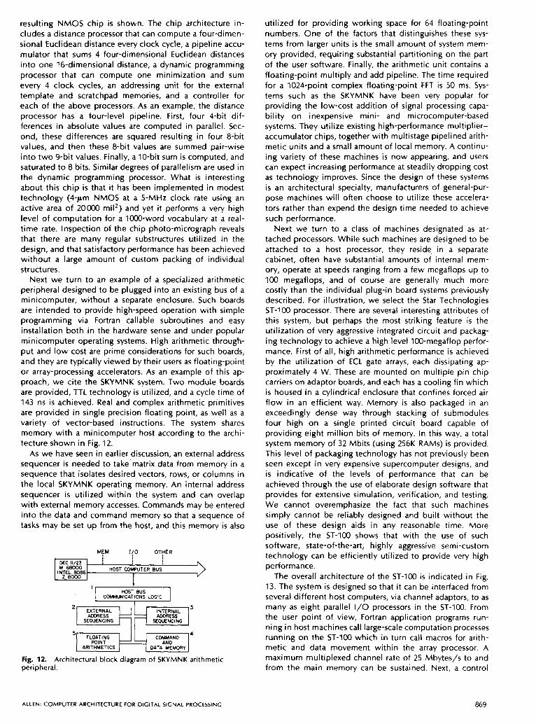
resulting NMOS chip is shown. The chip architecture in- cludes a distance processor that can compute a four-dimen- sional Euclidean distance every clock cycle, a pipeline accu- mulator that sums 4 four-dimensional Euclidean distances into one 16-dimensional distance, a dynamic programming processor that can compute one minimization and sum every 4 clock cycles, an addressing unit for the external template and scratchpad memories, and a controller for each of the above processors. As an example, the distance processor has a four-level pipeline. First, four 4-bit dif- ferences in absolute values are computed in parallel. Sec- ond, these differences are squared resulting in four 8-bit values, and then these 8-bit values are summed pair-wise into two 9-bit values. Finally, a 10-bit sum is computed, and saturated to 8 bits. Similar degrees of parallelism are used in the dynamic programming processor. What is interesting about this chip is that it has been implemented in modest technology (4-pm NMOS at a 5-MHz clock rate using an active area of 20000 mil2) and yet it performs a very high level of computation for a 1000-word vocabulary at a real- time rate. Inspection of the chip photo-micrograph reveals that there are many regular substructures utilized in the design, and that satisfactory performance has been achieved without a large amount of custom packing of individual structures.
Next we turn to an example of a specialized arithmetic peripheral designed to be plugged into an existing bus of a minicomputer, without a separate enclosure. Such boards are intended to provide high-speed operation with simple programming via Fortran callable subroutines and easy installation both in the hardware sense and under popular minicomputer operating systems. High arithmetic through- put and low cost are prime considerations for such boards, and they are typically viewed by their users as floating-point or array-processing accelerators. As an example of this ap- proach, we cite the SKYMNK system. Two module boards are provided, TTL technology is utilized, and a cycle time of 143 ns is achieved. Real and complex arithmetic primitives are provided in single precision floating point, as well as a variety of vector-based instructions. The system shares memory with a minicomputer host according to the archi- tecture shown in Fig. 12.
As we have seen in earlier discussion, an external address sequencer is needed to take'matrix data from memory in a sequence that isolates desired vectors, rows, or columns in the local SKYMNK operating memory. An internal address sequencer is utilized within the system and can overlap with external memory accesses. Commands may be entered into the data and command memory so that a sequence of tasks may be set up from the host, and this memory is also
MFM I (0 OTVER
M C 11/23 I M 6 8 0 0 0 8086 HOST COWUTER BUS z Boo0 I
I I COMMUNKATIONS LOGIC
M S T BUS
SEOUENCING SEQUENCING
COMMAND
ARITHMETICS DATA MEMORY
fig. 12. Architectural block diagram of SKYMNK arithmetic peripheral.
utilized for providing working space for 64 floating-point numbers. One of the factors that distinguishes these sys- tems from larger units is the small amount of system mem- ory provided, requiring substantial partitioning on the part of the user software. Finally, the arithmetic unit contains a floating-point multiply and add pipeline. The time required for a 1024-point complex floating-point FFT is 50 ms. Sys- tems such as the SKYMNK have been very popular for providing the low-cost addition of signal processing capa- bility on inexpensive mini- and microcomputer-based systems. They utilize existing high-performance multiplier- accumulator chips, together with multistage pipelined arith- metic units and a small amount of local memory. A continu- ing variety of these machines is now appearing, and users can expect increasing performance at steadily dropping cost as technology improves. Since the design of these systems is an architectural specialty, manufacturers of general-pur- pose machines will often choose to utilize these accelera- tors rather than expend the design time needed to achieve such performance.
Next we turn to a class of machines designated as at- tached processors. While such machines are designed to be attached to a host processor, they reside in a separate cabinet, often have substantial amounts of internal mem- ory, operate at speeds ranging from a few megaflops up to 100 megaflops, and of course are generally much more costly than the individual plug-in board systems previously described. For illustration, we select the Star Technologies ST-I00 processor. There are several interesting attributes of this system, but perhaps the most striking feature is the utilization of very aggressive integrated circuit and packag- ing technology to achieve a high level 100-megaflop perfor- mance. First of all, high arithmetic performance is achieved by the utilization of ECL gate arrays, each dissipating ap- proximately 4 W. These are mounted on multiple pin chip carriers on adaptor boards, and each has a cooling fin which is housed in a cylindrical enclosure that confines forced air f low in an efficient way. Memory is also packaged in an exceedingly dense way through stacking of submodules four high on a single printed circuit board capable of providing eight million bits of memory. In this way, a total system memory of 32 Mbits (using 256K RAMS) is provided, This level of packaging technology has not previously been seen except in very expensive supercomputer designs, and is indicative of the levels of performance that can be achieved through the use of elaborate design software that provides for extensive simulation, verification, and testing. We cannot overemphasize the fact that such machines simply cannot be reliably designed and built without the use of these design aids in any reasonable time. More positively, the ST-I00 shows that with the use of such software, state-of-the-art, highly aggressive semi-custom technology can be efficiently utilized to provide very high performance.
The overall architecture of the ST-100 is indicated in Fig. 13. The system is designed so that it can be interfaced from several different host computers, via channel adaptors, to as many as eight parallel 1/0 processors in the ST-100. From the user point of view, Fortran application programs run- ning in host machines call large-scale computation processes running on the ST-I00 which in turn call macros for arith- metic and data movement within the array processor. A maximum multiplexed channel rate of 25 Mbytes/s to and from the main memory can be sustained. Next, a control
ALLEN: COMPUTER ARCHITECTURE FOR DIGITAL SIGNAL PROCESSING 869
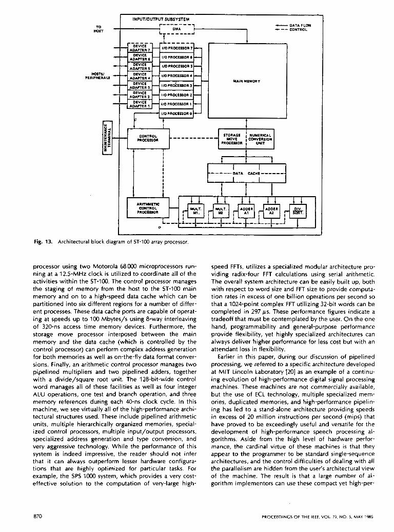
INPUTlOUTPUT SUBSYSTEM
To HOST
- DATA f LOYI 0-- CONTROL
MAIN MEMORY
t
- 1 I I I
I !
Fig. 13. Architectural block diagram of ST-I00 array processor.
processor using two Motorola Moo0 microprocessors run- ning at a 12.5-MHz clock is utilized to coordinate all of the activities within the ST-100. The control processor manages the staging of memory from the host to the ST-I00 main memory and on to a high-speed data cache which can be partitioned into six different regions for a number of differ- ent processes. These data cache ports are capable of operat- ing at speeds up to 100 Mbytes/s using 8-way interleaving of 320-ns access time memory devices. Furthermore, the storage move processor interposed between the main memory and the data cache (which is controlled by the control processor) can perform complex address generation for both memories as well as on-the-fly data format conver- sions. Finally, an arithmetic control processor manages two pipelined multipliers and two pipelined adders, together with a divide/square root unit. The 128-bit-wide control word manages all of these facilities as well as four integer ALU operations, one test and branch operation, and three memory references during each 40-ns clock cycle. In this machine, we see virtually all of the high-performance archi- tectural structures used. These include pipelined arithmetic units, multiple hierarchically organized memories, special- ized control processors, multiple input/output processors, specialized address generation and type conversion, and very aggressive technology. While the performance of this system is indeed impressive, the reader should not infer that it can always outperform lesser hardware configura- tions that are highly optimized for particular tasks. For example, the SPS IO00 system, which provides a very cost- effective solution to the computation of very-large high-
speed FFTs, utilizes a specialized modular architecture pro- viding radix-four FFT calculations using serial arithmetic. The overall system architecture can be easily built up, both with respect to word size and FFT size to provide computa- tion rates in excess of one billion operations per second so that a 1024-point complex FFT utilizing 32-bit words can be completed in 297 ks. These performance figures indicate a tradeoff that must be contemplated by the user. O n the one hand, programmability and general-purpose performance provide flexibility, yet highly specialized architectures can always deliver higher performance for less cost but with an attendant loss in flexibility.
Earlier in this paper, during our discussion of pipelined processing, we referred to a specific architecture developed at MIT Lincoln Laboratory [20] as an example of a continu- ing evolution of high-performance digital signal processing machines. These machines are not commercially available, but the use of ECL technology, multiple specialized mem- ories, duplicated memories, and high-performance pipelin- ing has led to a stand-alone architecture providing speeds in excess of 20 million instructions per second (mips) that have proved to be exceedingly useful and versatile for the development of high-performance speech processing al- gorithms. Aside from the high level of hardware perfor- mance, the cardinal virtue of these machines is that they appear to the programmer to be standard single-sequence architectures, and the control difficulties of dealing with all the parallelism are hidden from the user's architectural view of the machine. The result is that a large number of al- gorithm implementors can use these compact yet high-per-
870 PROCEEDINGS O F THE IEEE, VOL. 73, NO. 5, M A Y 1585
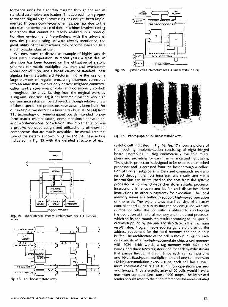
formance units for algorithm research through the use of standard assemblers and loaders. This approach to high-per- formance digital signal processing has not yet been imple- mented through commercial offerings, perhaps due to the fact that the performance of these machines involves timing tolerances that cannot be readily realized in a produc- tion-line environment. Nevertheless, with the advent of new design and testing software already mentioned, the great utility of these machines may become available to a much broader class of user.
We now move to discuss an example of highly special- ized systolic computation. In recent years, a great deal of attention has been focused on the utilization of systolic schemes for matrix multiplication, one- and two-dimen- sional convolution, and a broad variety of standard linear algebra tasks. Systolic architectures involve the use of a large number of regular processing elements connected into an array that involves only nearest neighbor communi- cation and a streaming of data (and occasionally control) throughout the array. Starting from the original work by Kung and Leiserson [43], it has become clear that very high performance rates can be achieved, although relatively few of these specialized processors have actually been built. For our example, we describe a linear array built at ESL [44] from TTL technology on wire-wrapped boards intended to per- form matrix multiplication, one-dimensional convolution, and two-dimensional convolution. This implementation was a proof-of-concept design, and utilized only off-the-shelf components that are readily available. The overall architec- ture of the system is shown in Fig. 14, and the linear array is indicated in Fig. 1 5 with the detailed structure of each
INTERFACE
I SYSTOLIC .WOCESOR I Fig. 14. Experimental system architecture for ESL systolic array.
L
" CELL
M E M O R Y
Fig. 15. ESL linear systolic array
MEMORY CELL
I I
I I <> OUTPUT STREAM
Fig. 16. Systolic cell architecture for ESL linear systolic array.
Fig. 17. Photograph of ESL linear systolic array.
systolic cell indicated in Fig. 16. Fig. 17 shows a picture of the resulting implementation consisting of eight hinged board assemblies utilizing commercially available multi- pliers and providing for easy maintenance and debugging. The systolic processor is designed to be used as an attached processor and is accessed from the host through a collec- tion of Fortran subprograms. Data and commands are trans- ferred through the host interface, and results and status information can be returned to the host from the systolic processor. A command dispatcher stores systolic processor instructions in a command buffer and dispatches these instructions to other subsystems for execution. The local memory serves as a buffer to support high-speed operation of the array. The systolic array itself consists of an array controller and a linear array that can be configured with any number of cells. The controller i s utilized to synchronize the operation of the local memory and the output processor which shifts and rounds the results according to the specifi- cations supplied by the user and also detects the maximum result value. Programmable address generators provide the address sequences for the local memory and the output buffer. The architecture of the cell is shown in Fig. 16. Each cell consists of a multiply-accumulate chip, a cell memory with 1024 16-bit words, a tag memory with 1024 4-bit words, and three latch registers, one for each systolic stream that passes through the cell. Since each cell can perform one 16-bit fixed-point multiplication and one full precision (42-bit) accumulation every 200 ns, each cell has a maxi- mum computational rate of 10 million operations per sec- ond (mops). Thus a systolic array of 20 cells would have a maximum computational rate of 200 mops. The interested reader should refer to the cited references for more detailed
ALLEN. COMPUTER ARCHITECTURE F O R DIGITAL SIGNAL PROCESSING 871
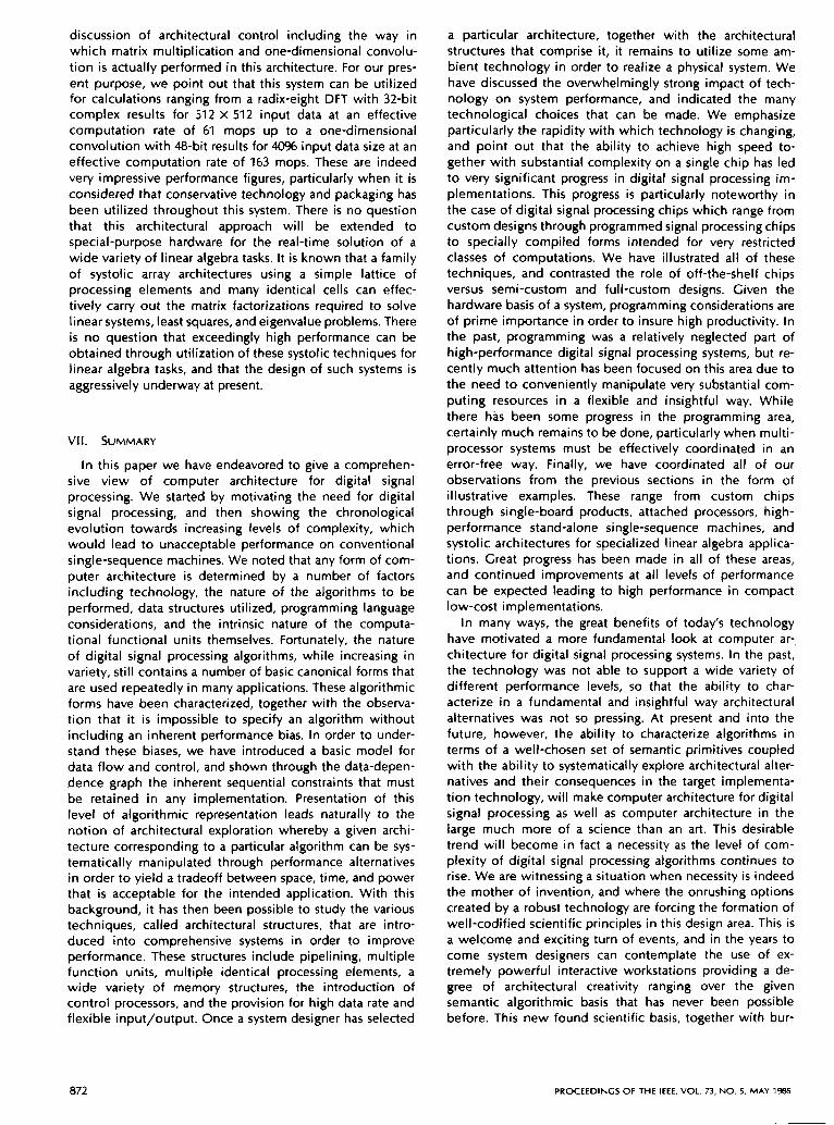
discussion of architectural control including the way in which matrix multiplication and one-dimensional convolu- tion is actually performed in this architecture. For our pres- ent purpose, we point out that this system can be utilized for calculations ranging from a radix-eight DFT with 32-bit complex results for 512 X 512 input data at an effective computation rate of 61 mops up to a one-dimensional convolution with 48-bit results for 4096 input data size at an effective computation rate of 163 mops. These are indeed very impressive performance figures, particularly when it is considered that conservative technology and packaging has been utilized throughout this system. There is no question that this architectural approach will be extended to special-purpose hardware for the real-time solution of a wide variety of linear algebra tasks. It is known that a family of systolic array architectures using a simple lattice of processing elements and many identical cells can effec- tively carry out the matrix factorizations required to solve linear systems, least squares, and eigenvalue problems. There is no question that exceedingly high performance can be obtained through utilization of these systolic techniques for linear algebra tasks, and that the design of such systems is aggressively underway at present.
VII. SUMMARY
In this paper we have endeavored to give a comprehen- sive view of computer architecture for digital signal processing. We started by motivating the need for digital signal processing, and then showing the chronological evolution towards increasing levels of complexity, which would lead to unacceptable performance on conventional single-sequence machines. We noted that any form of com- puter architecture is determined by a number of factors including technology, the nature of the algorithms to be performed, data structures utilized, programming language considerations, and the intrinsic nature of the computa- tional functional units themselves. Fortunately, the nature of digital signal processing algorithms, while increasing in variety, still contains a number of basic canonical forms that are used repeatedly in many applications. These algorithmic forms have been characterized, together with the observa- tion that it is impossible to specify an algorithm without including an inherent performance bias. In order to under- stand these biases, we have introduced a basic model for data flow and control, and shown through the data-depen- dence graph the inherent sequential constraints that must be retained in any implementation. Presentation of this level of algorithmic representation leads naturally to the notion of architectural exploration whereby a given archi- tecture corresponding to a particular algorithm can be sys- tematically manipulated through performance alternatives in order to yield a tradeoff between space, time, and power that is acceptable for the intended application. With this background, it has then been possible to study the various techniques, called- architectural structures, that are intro- duced into comprehensive systems in order to improve performance. These structures include pipelining, multiple function units, multiple identical processing elements, a wide variety of memory structures, the introduction of control processors, and the provision for high data rate and flexible input/output. Once a system designer has selected
a particular architecture, together with the architectural structures that comprise it, it remains to utilize some am- bient technology in order to realize a physical system. We have discussed the overwhelmingly strong impact of tech- nology on system performance, and indicated the many technological choices that can be made. We emphasize particularly the rapidity with which technology i s changing, and point out that the ability to achieve high speed to- gether with substantial complexity on a single chip has led to very significant progress in digital signal processing im- plementations. This progress is particularly noteworthy in the case of digital signal processing chips which range from custom designs through programmed signal processing chips to specially compiled forms intended for very restricted classes of computations. We have illustrated all of these techniques, and contrasted the role of off-the-shelf chips versus semi-custom and full-custom designs. Given the hardware basis of a system, programming considerations are of prime importance in order to insure high productivity. In the past, programming was a relatively neglected part of high-performance digital signal processing systems, but re- cently much attention has been focused on this area due to the need to conveniently manipulate very substantial com- puting resources in a flexible and insightful way. While there has been some progress in the programming area, certainly much remains to be done, particularly when multi- processor systems must be effectively coordinated in an error-free way. Finally, we have coordinated all of our observations from the previous sections in the form of illustrative examples. These range from custom chips through single-board products, attached processors, high- performance stand-alone single-sequence machines, and systolic architectures for specialized linear algebra applica- tions. Great progress has been made in all of these areas, and continued improvements at all levels of performance can be expected leading to high performance in compact low-cost implementations.
In many ways, the great benefits of today's technology have motivated a more fundamental look at computer ar- chitecture for digital signal processing systems. In the past, the technology was not able to support a wide variety of different performance levels, so that the ability to char- acterize in a fundamental and insightful way architectural alternatives was not so pressing. At present and into the future, however, the ability to characterize algorithms in terms of a well-chosen set of semantic primitives coupled with the ability to systematically explore architectural alter- natives and their consequences in the target implementa- tion technology, will make computer architecture for digital signal processing as well as computer architecture in the large much more of a science than an art. This desirable trend will become in fact a necessity as the level of com- plexity of digital signal processing algorithms continues to rise. We are witnessing a situation when necessity is indeed the mother of invention, and where the onrushing options created by a robust technology are forcing the formation of well-codified scientific principles in this design area. This is a welcome and exciting turn of events, and in the years to come system designers can contemplate the use of ex- tremely powerful interactive workstations providing a de- gree of architectural creativity ranging over the given semantic algorithmic basis that has never been possible before. This new found scientific basis, together with bur-
872 PROCEEDINGS O F THE IEEE, VOL. 73, N O . 5 , M A Y 1985
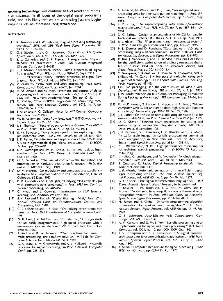
geoning technology, will continue to fuel rapid and impres- sive advances in all facets of the digital signal processing field, and it i s likely that we are witnessing just the begin- ning of such an impressive long-term trend.
REFERENCES
[l] K. Bromley and J. Whitehouse, “Signal processing technology overview,” SPIE, vol. 298 (Real Time Signal Processing IV,
[2] C. L. Steele, Jr., and C. J. Sussman, ”Constraints,” APL Quote Quad, vol. 9, no. 4, pt. 1, pp. 208-225, June 1979.
[3] 5. L. Carverick and E. A. Pierce, “A single wafer 16-point 16-MHz FFT processor,” in Proc. 7983 Custom Integrated Circuits Conf., pp. 244-248.
[4] S. J. Mason, “feedback theory-Some properties of signal f low graphs,” Proc. IRE, vol. 41, pp. 920-926, Sept. 1953. -, “Feedback theory-Further properties of signal flow graphs,” Proc. IRE, vol. 44, pp. 920-926, July 1956.
(51 V. Zakharov, “Parallelism and array processing,” /€€E Trans. Cornput., vol. C-33, no. 1, pp. 45-78, Jan. 1934.
[6] H. M. Ahmed and M. Morf, “Synthesis and control of signal processing architectures based on rotations,” in VLSl 87, J. P. Gray, Ed. New York: Academic Press, 1981, pp. 43-52.
[7] C. Volder, “The CORDIC trigonometric computing tech-
330-334, Sept. 1959. nique,” IRE Trans. Electron. Comput., vol. EC-8, no. 3, pp.
[8] J. Allen and R. C. Gallager, Notes for MIT Course “Computa- tion Structures,” 1975.
[9] W. 6. Ackerman, “Data flow languages,” /€E€ Computer, vol. 15, no. 2, pp. 15-25, Feb. 1982.
[lo] J. E. Thornton, “Parallel operation in the Control Data 6600,’’ in Proc. AFIPS-FJCC, vol. 26, pt. 2, pp. 33-40, 1964.
[ l l ] R. M. Tomasulo, “An efficient algorithm for exploiting multi- ple arithmetic units,” lBM/ . Res. Devel., pp. 25-33, Jan. 1%7.
[12] J. R. Fisher, “Architecture and applications of the SPS-41 and SPS-81 programmable digital signal processors,” in €ASCON 74 Rec., pp. 674-678.
[13] J. A. Darringer and W. H. Joyner, Jr., “A new look at logic synthesis,” in Proc. 77th Design Automation Conf., pp. 543-549, 1980.
[I41 C. 5. Miranker, “The use of conflict in the translation and optimization of hardware description languages,” Ph.D. dis- sertation, MIT EECS Dep., 1979.
[15] 0. M. Henrot, “On modularity and computational parallelism in digital filter implementations,” Ph.D. dissertation, Univ. of Colorado, EE Dep., 1983.
[16] P. R. Cappello and K. Steiglitz, “Unifying VLSl array designs with geometric transformations,” in Proc. 7983 Int. Conf. on Parallel Processing, pp. 448-457.
[I71 C. Mead and L. Conway, Introduction to VLSl Systems. Reading, MA: Addison-Wesley, 1980.
[18] 5. K. Rao and T. Kailath, “Digital filtering in VLSI,” Proc. 2nd Annual Allerton Conf. on Communication, Control, and Computing, Oct. 1984.
[I91 C. E. Leiserson and J. B. Saxe, “Optimizing synchronous sys- tems,” in Proc. /E€€ Foundations o f Computer Science Conf., 1981.
[20] D. 6. Paul, J. A. Feldman, and V. J. Sferrino, ”A design study for an easily programmable, high-speed processor with a general-purpose architecture,” MIT Lincoln Lab. Tech. Note
[21] Arvind and R. A. lannucci, “Two fundamental issues in multi-processing: The dataflow solution,” MIT Lab. for Com- puter Science Tech. Memo 241, Sept. 1983.
[22] C. A. Frank, E. M. Creenawalt, and A. V. Kulkarni. “A systolic processor for signal processing,” in Proc. 7982 Nat. Computer Conf., pp. 225-231.
1981), pp. 102-106.
1980-50,1980.
[23) 6. Ackland, N. Weste, and D. J. Burr, “An integrated multi- processing array for time warp pattern matching,” in Proc. 8th Annu. Symp. on Computer Architecture, pp. 197-215, May 1981.
[24] S. Y. Kung, “On supercomputing with systolic/wavefront array processors,” Proc. I€€€, vol. 72, no. 7, pp. 867-8&1, July 1984.
[25] D. C. Baltus, “Design of an assembler of NMOS fast parallel fractional multipliers,” B.S. thesis, MIT EECS Dep., May 1983.
[26] R. L. Rivest, “The ’PI’ (placement and interconnect) system,” in Proc. 79th Design Automation Conf., pp. 475-481, ‘1982.
[27] P. 6. Denyer and D. Renshaw, “Case studies in VLSl signal processing using a silicon compiler,” in Proc. 7983 Int. Conf. on Acoustics, Speech, and Signal Processing, pp. 939-942.
[28] R. lain, J. Vandewalle, and H. De Man, “Efficient CAD tools for the coefficient optimization of arbitrary integrated digital filers,” in Proc. 79% Int. Conf. on Acoustics, Speech, and Signal Processing, pp. 30.11.1 -30.1 1.4.
(291 Y. Nakayama, S. Katsuhiko, H. Shimizu, N. Yokoyama, and A. Shibatomi, “A GaAs 16 X 16b parallel multiplier using self- alignment technology,” in 7983 Solid-State Circuits Conf. Dig. Tech. Papers, pp. 48-49.
[30] On IBM packaging, see the entire issues of ISM 1. Res. Develop., vol. 26, no. 3, May 1982 and vol. 27, no. 1, Jan. 1983.
(311 J , W. Balde, “Report on IEEE Computer Packaging Committee
1934. Spring Packaging Workshop,” /€E€ Computer, pp. 83-86, Jan.
[32] K. McDonough, E. Caudel, S. Magar, and A. Leigh, “Micro- computer with 32-bit arithmetic does high-precision number crunching,” Electronics, pp. 105-110, Feb. 24, 1982.
[33] J. I . Raffel, “On the use of nonvolatile programmable links for restructurable VLSI,” in Proc. Caltech Conf. on VLSI, Jan. 1979.
(341 D. C. Shaver, “Electron beam techniques for testing and restructuring of wafer-scale integrated circuits,” MIT EECS Dept. Ph.D. dissertation, 1981.
[35] J. A. Feldman, S. L. Carverick, F. M. Rhodes, and J. R. Mann, “A wafer scale integration systolic processor for connected word recognition,” in Proc. 7984 Int. Conf. on Acoustics, Speech, and Signal Processing, pp. 256.4.1-258.4.4.
[36] P. E. Blankenship, “LDVT: High performance minicomputer for real-time speech processing,” in €ASCON 75 Rec., pp. 21 4a-214g.
[37] J. Kelley, C. Lochbaum, and V. Vyssotsky, “A block diagram compiler,” Bell Syst. Tech. J., vol. 40, no. 3, May 1%1.
[38] 6. Gold and C. Rader, Digital Processing o f Signals. New York: McCraw-Hill, 1%9.
[39] L. R. Morris, “Automatic generation of time efficient digital signal processing software,” I€€€ Trans. Acoust., Speech, S i g nal Process., vol. ASSP-25, no. 1, pp. 74-79. Feb. 1977.
(401 C. E. Kopec, “The signal representation language SRL,” I€€€ Trans. Acoust., Speech, Signal Process., to be published.
[41] R. Kavaler, R. W. Brodersen, T. C. Noll, M. Lowy, and H. Murveit, “A dynamic time warp IC for a one thousand word recognition system,” in Proc. 7 9 8 4 Int. Conf. on Acoustics, Speech, and Signal Processing, pp. 258.6.1-256.6.4.
[42] H. Sakoe and 5. Chiba, “Dynamic programming algorithm optimization for spoken word recognition,” / € € E Trans.
1978. Acoust. Speech, Signal Process., vol. ASSP-26, pp. 43-49, Feb.
(431 C. E. Leiserson, Area-Efficient VLSI Computation. Cam- bridge, MA: MIT Press, 1983.
(441 A. V. Kulkarni and D. W. L. Yen, ”Systolic processing and an implementation for signal and image processing,” /E€€ Trans. Comput., vol. C-31, no. 10, pp. 1ooO-1009, Oct. 1982.
(451 J. S. Thompson and S. K. Tewksbury, “LSI signal processor architecture for telecommunications applications,” I€€€ Trans. Acoust. Speech, Signal Process., vol. ASSP-30, pp. 619-632, Aug. 1982.
[46] J. Allen, “Computer architecture for signal processing,” Proc. / € € E , vol. 63, no. 4, pp. 624-633, Apr. 1975.
ALLEN: COMPUTER ARCHITECTURE FOR DIGITAL SIGNAL PROCESSING 873