Embed Size (px)
Citation preview

Computer Architecture
Lecture 5: Multi-Cycle and Microprogrammed Microarchitectures
Dr. Ahmed SallamSuez Canal University
Spring 2015
Based on original slides by Prof. Onur Mutlu
Agenda for Today & Next Few Lectures Single-cycle Microarchitectures
Multi-cycle and Microprogrammed Microarchitectures
Pipelining
2
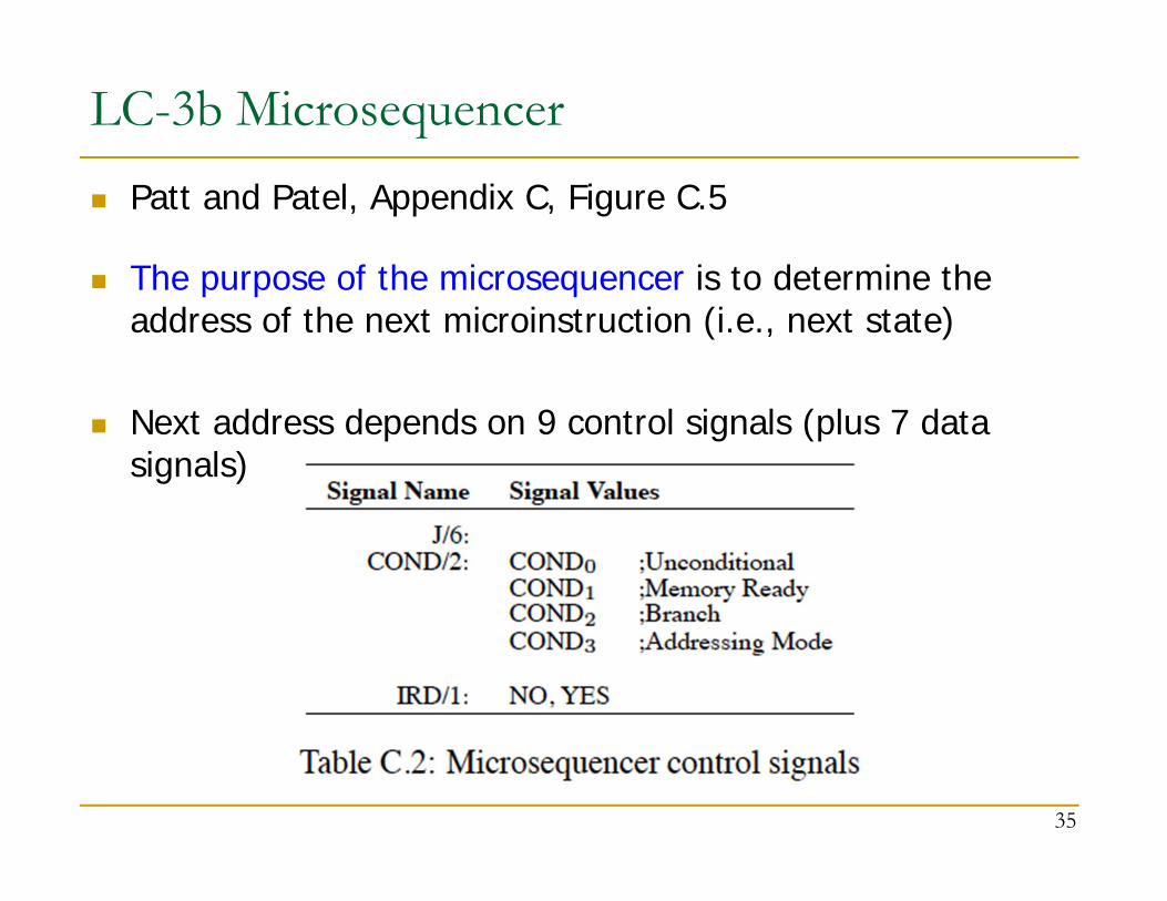
Readings for Today P&P, Revised Appendix C
Microarchitecture of the LC-3b Appendix A (LC-3b ISA) will be useful in following this
P&H, Appendix D Mapping Control to Hardware
Maurice Wilkes, “The Best Way to Design an Automatic Calculating Machine,” Manchester Univ. Computer Inaugural Conf., 1951.
3

Last Lecture Intro to Microarchitecture: Single-cycle Microarchitectures
Single-cycle vs. multi-cycle Instruction processing “cycle” Datapath vs. control logic Hardwired vs. microprogrammed control Performance analysis: Execution time equation
Detailed walkthrough of a single-cycle MIPS implementation Datapath Control logic Critical path analysis
(Micro) architecture design principles
4

Review: A Key System Design Principle Keep it simple
“Everything should be made as simple as possible, but no simpler.” Albert Einstein
And, keep it low cost: “An engineer is a person who can do for a dime what any fool can do for a dollar.”
For more, see: Butler W. Lampson, “Hints for Computer System Design,” ACM
Operating Systems Review, 1983. http://research.microsoft.com/pubs/68221/acrobat.pdf
5

Review: (Micro)architecture Design Principles
Critical path design Find and decrease the maximum combinational logic delay Break a path into multiple cycles if it takes too long
Bread and butter (common case) design Spend time and resources on where it matters most
i.e., improve what the machine is really designed to do
Common case vs. uncommon case
Balanced design Balance instruction/data flow through hardware components Design to eliminate bottlenecks: balance the hardware for the
work
6
Review: Single-Cycle Design vs. Design Principles
Critical path design
Common case design (Bread and butter)
Balanced design
How does a single-cycle microarchitecture fare in light of these principles?
7
Multi-Cycle Microarchitectures
8
Multi-Cycle Microarchitectures Goal: Let each instruction take (close to) only as much time
it really needs
Idea Determine clock cycle time independently of instruction
processing time Each instruction takes as many clock cycles as it needs to take
Multiple state transitions per instruction The states followed by each instruction is different
9
Benefits of Multi-Cycle Design Critical path design
Can keep reducing the critical path independently of the worst-case processing time of any instruction
Bread and butter (common case) design Can optimize the number of states it takes to execute “important”
instructions that make up much of the execution time
Balanced design No need to provide more capability or resources than really
needed An instruction that needs resource X multiple times does not require
multiple X’s to be implemented Leads to more efficient hardware: Can reuse hardware components
needed multiple times for an instruction10

Remember: Performance Analysis Execution time of an instruction
{CPI} x {clock cycle time}
Execution time of a program Sum over all instructions [{CPI} x {clock cycle time}] {# of instructions} x {Average CPI} x {clock cycle time}
Single cycle microarchitecture performance CPI = 1 Clock cycle time = long
Multi-cycle microarchitecture performance CPI = different for each instruction
Average CPI hopefully small
Clock cycle time = short11
Now, we have two degrees of freedomto optimize independently
A Multi-Cycle MicroarchitectureA Closer Look
12

Microprogrammed Multi-Cycle uArch Key Idea for Realization
One can implement the “process instruction” step as a finite state machine that sequences between states and eventually returns back to the “fetch instruction” state
A state is defined by the control signals asserted in it
Control signals for the next state determined in current state
13
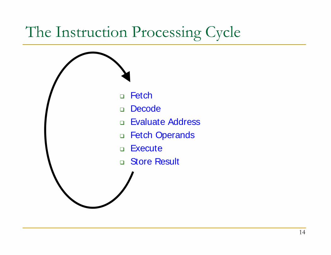
The Instruction Processing Cycle
Fetch Decode Evaluate Address Fetch Operands Execute Store Result
14
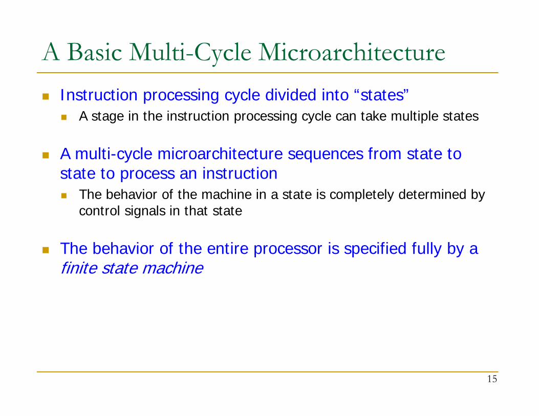
A Basic Multi-Cycle Microarchitecture Instruction processing cycle divided into “states”
A stage in the instruction processing cycle can take multiple states
A multi-cycle microarchitecture sequences from state to state to process an instruction The behavior of the machine in a state is completely determined by
control signals in that state
The behavior of the entire processor is specified fully by a finite state machine
15
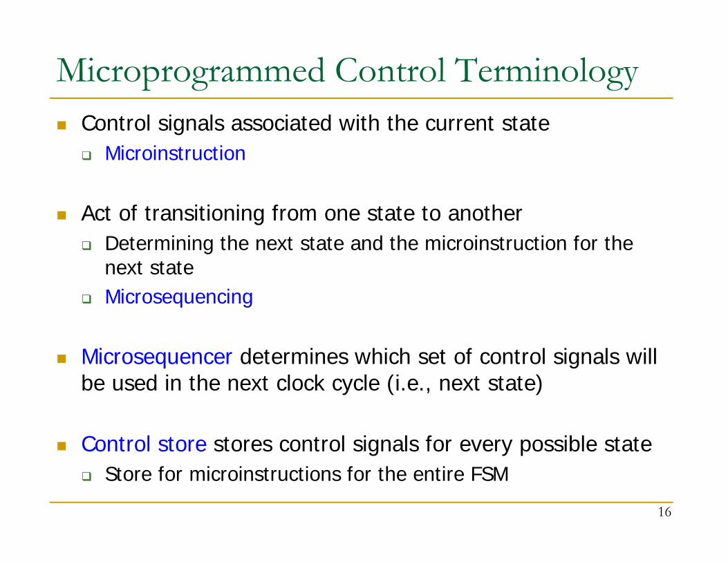
Microprogrammed Control Terminology Control signals associated with the current state
Microinstruction
Act of transitioning from one state to another Determining the next state and the microinstruction for the
next state Microsequencing
Microsequencer determines which set of control signals will be used in the next clock cycle (i.e., next state)
Control store stores control signals for every possible state Store for microinstructions for the entire FSM
16
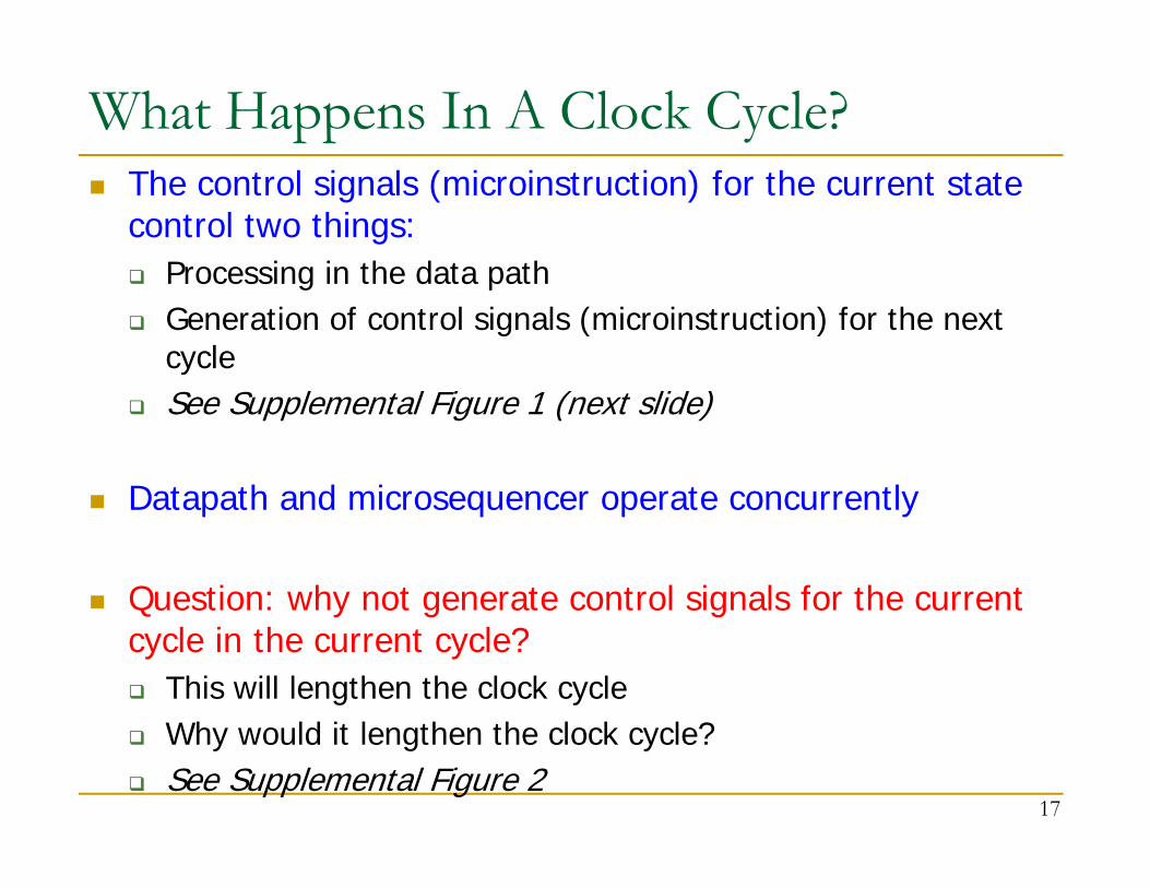
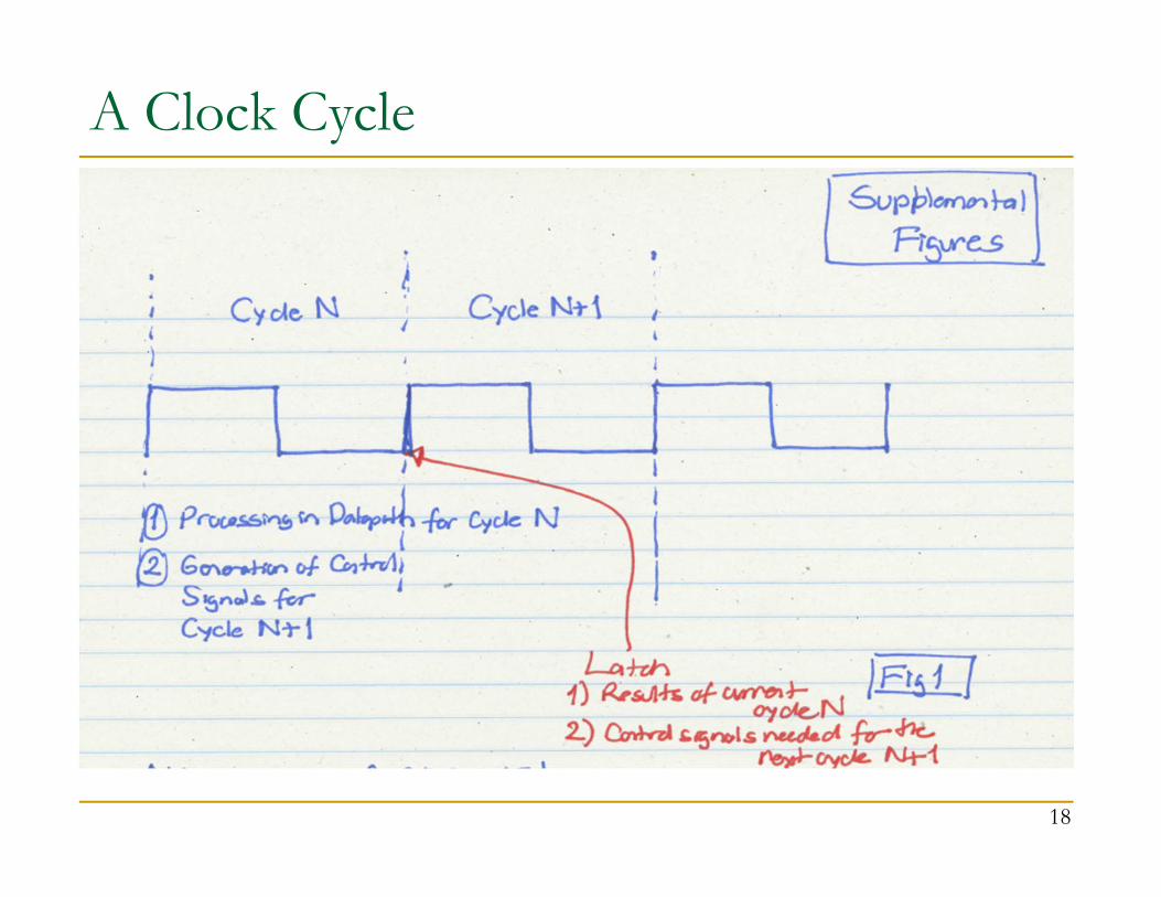
What Happens In A Clock Cycle? The control signals (microinstruction) for the current state
control two things: Processing in the data path Generation of control signals (microinstruction) for the next
cycle See Supplemental Figure 1 (next slide)
Datapath and microsequencer operate concurrently
Question: why not generate control signals for the current cycle in the current cycle? This will lengthen the clock cycle Why would it lengthen the clock cycle? See Supplemental Figure 2
17
A Clock Cycle
18

A Bad Clock Cycle!
19
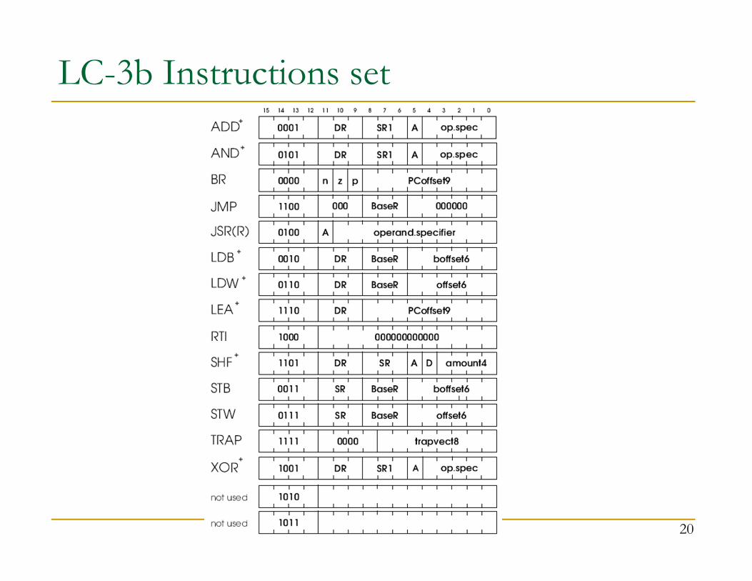
LC-3b Instructions set
20
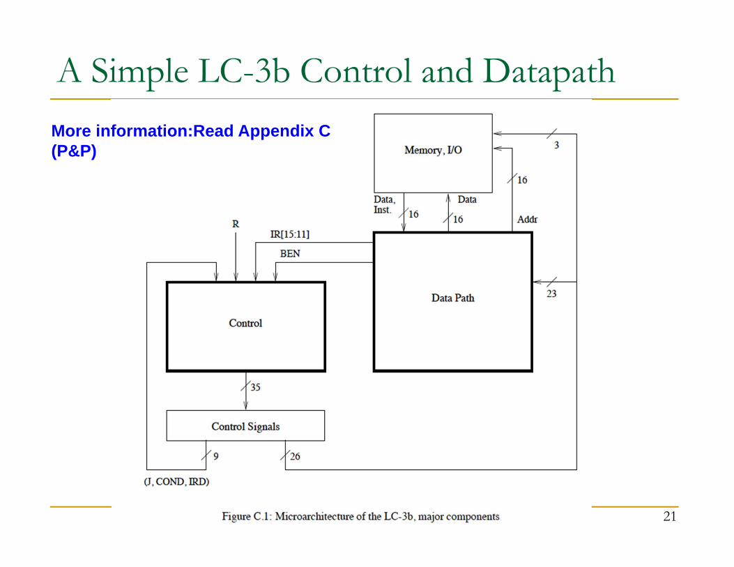
A Simple LC-3b Control and Datapath
21
More information:Read Appendix C (P&P)
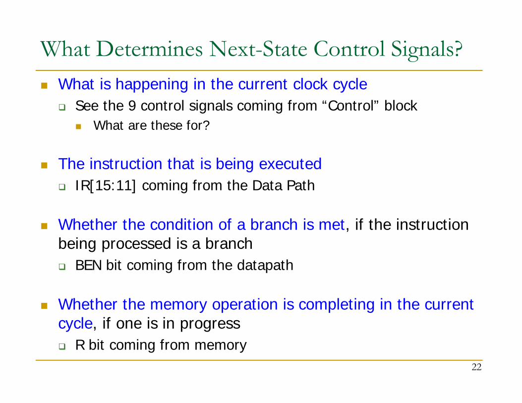
What Determines Next-State Control Signals? What is happening in the current clock cycle
See the 9 control signals coming from “Control” block What are these for?
The instruction that is being executed IR[15:11] coming from the Data Path
Whether the condition of a branch is met, if the instruction being processed is a branch BEN bit coming from the datapath
Whether the memory operation is completing in the current cycle, if one is in progress R bit coming from memory
22

The State Machine for Multi-Cycle Processing The behavior of the LC-3b uarch is completely determined by
the 35 control signals and additional 7 bits that go into the control logic from the datapath
35 control signals completely describe the state of the control structure
We can completely describe the behavior of the LC-3b as a state machine, i.e. a directed graph of Nodes (one corresponding to each state) Arcs (showing flow from each state to the next state(s))
23

An LC-3b State Machine Each state must be
uniquely specified Done by means of state
variables
31 distinct states in this LC-3b state machine Encoded with 6 state
variables
Examples State 18,19 correspond
to the beginning of the instruction processing cycle
Fetch phase: state 18, 19 state 33 state 35
Decode phase: state 32
24
R
PC<! BaseR
To 18
12
To 18
To 18
RR
To 18
To 18
To 18
MDR<! SR[7:0]
MDR <! M
IR <! MDR
R
DR<! SR1+OP2*set CC
DR<! SR1&OP2*set CC
[BEN]
PC<! MDR
32
1
5
0
0
1To 18
To 18 To 18
R R
[IR[15:12]]
28
30
R7<! PCMDR<! M[MAR]
set CC
BEN<! IR[11] & N + IR[10] & Z + IR[9] & P
9DR<! SR1 XOR OP2*
4
22
To 111011
JSRJMP
BR
1010
To 10
21
200 1
LDB
MAR<! B+off6
set CC
To 18
MAR<! B+off6
DR<! MDRset CC
To 18
MDR<! M[MAR]
25
27
3762
STW STBLEASHF
TRAP
XOR
AND
ADD
RTI
To 8
set CC
set CCDR<! PC+LSHF(off9, 1)
14
LDW
MAR<! B+LSHF(off6,1) MAR<! B+LSHF(off6,1)
PC<! PC+LSHF(off9,1)
33
35
DR<! SHF(SR,A,D,amt4)
NOTESB+off6 : Base + SEXT[offset6]
R
MDR<! M[MAR[15:1]’0]
DR<! SEXT[BYTE.DATA]
R
29
31
18, 19
MDR<! SR
To 18
R R
M[MAR]<! MDR
16
23
R R
17
To 19
24
M[MAR]<! MDR**
MAR<! LSHF(ZEXT[IR[7:0]],1)
15To 18
PC+off9 : PC + SEXT[offset9]
MAR <! PCPC <! PC + 2
*OP2 may be SR2 or SEXT[imm5]** [15:8] or [7:0] depending on MAR[0]
[IR[11]]
PC<! BaseR
PC<! PC+LSHF(off11,1
R7<! PC
R7<! PC
13
LC-3b State Machine: Some Questions How many cycles does the fastest instruction take?
How many cycles does the slowest instruction take?
Why does the BR take as long as it takes in the FSM?
What determines the clock cycle time?
25

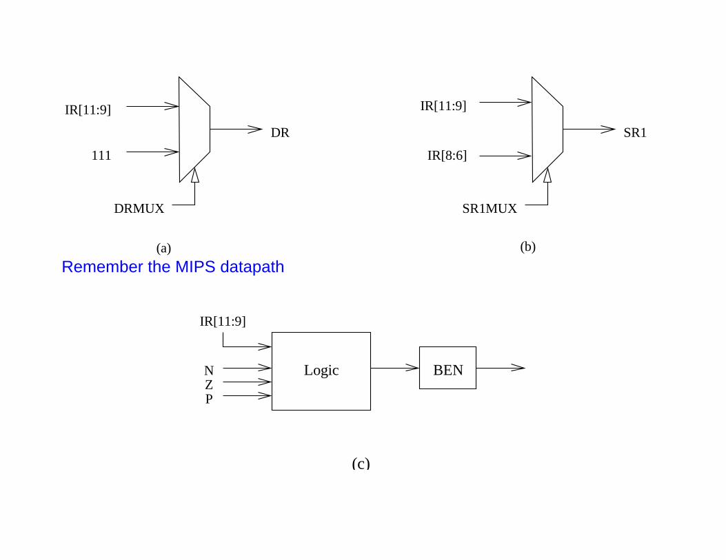
LC-3b Datapath Patt and Patel, Appendix C, Figure C.3
Single-bus datapath design At any point only one value can be “gated” on the bus (i.e.,
can be driving the bus) Advantage: Low hardware cost: one bus Disadvantage: Reduced concurrency – if instruction needs the
bus twice for two different things, these need to happen in different states
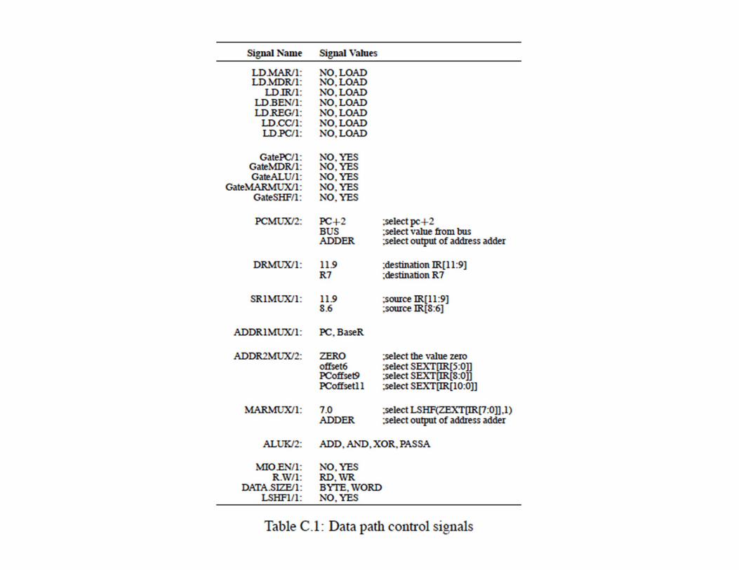
Control signals (26 of them) determine what happens in the datapath in one clock cycle Patt and Patel, Appendix C, Table C.1
26

DR
IR[11:9]
111
DRMUX
(a)
SR1
SR1MUX
IR[11:9]
IR[8:6]
(b)
Logic BEN
PZN
IR[11:9]
(c)
Remember the MIPS datapath

LC-3b Datapath: Some Questions How does instruction fetch happen in this datapath
according to the state machine?
What is the difference between gating and loading?
Is this the smallest hardware you can design?
30
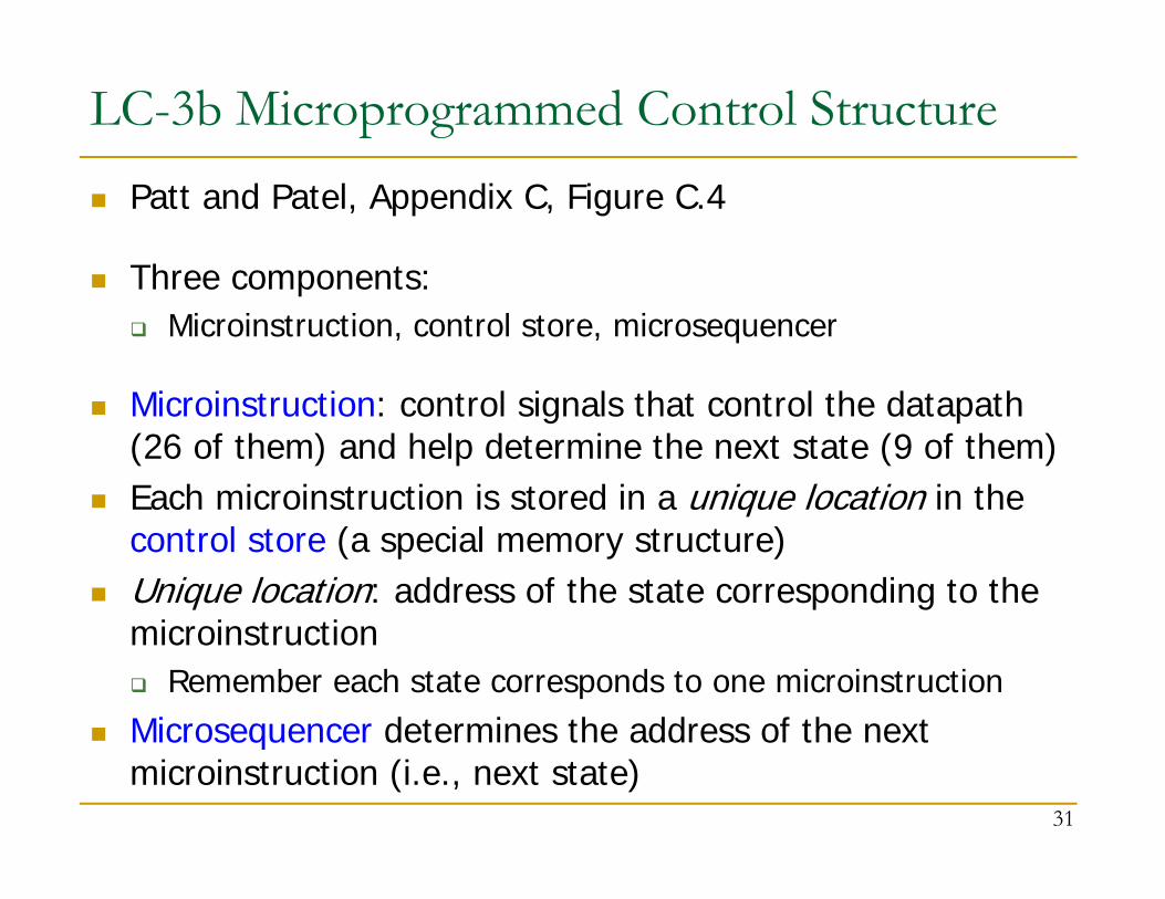
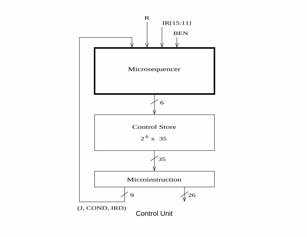
LC-3b Microprogrammed Control Structure Patt and Patel, Appendix C, Figure C.4
Three components: Microinstruction, control store, microsequencer
Microinstruction: control signals that control the datapath(26 of them) and help determine the next state (9 of them)
Each microinstruction is stored in a unique location in the control store (a special memory structure)
Unique location: address of the state corresponding to the microinstruction Remember each state corresponds to one microinstruction
Microsequencer determines the address of the next microinstruction (i.e., next state)
31
Microinstruction
R
Microsequencer
BEN
x2
Control Store6
IR[15:11]
6
(J, COND, IRD)
269
35
35
Control Unit
IRD
Address of Next State
6
6
0,0,IR[15:12]
J[5]
Branch ReadyModeAddr.
J[0]J[1]J[2]
COND0COND1
J[3]J[4]
R IR[11]BEN
LC-3b Microsequencer

J LD.P
C
LD.B
EN
LD.IR
LD.M
DR
LD.M
AR
LD.R
EGLD
.CC
Cond
IRD
GateP
CGa
teMDR
GateA
LUGa
teMAR
MUX
GateS
HFPC
MUX
DRM
UXSR
1MUX
ADDR
1MUX
ADDR
2MUX
MAR
MUX
010000 (State 16)010001 (State 17)
010011 (State 19)010010 (State 18)
010100 (State 20)010101 (State 21)010110 (State 22)010111 (State 23)011000 (State 24)011001 (State 25)011010 (State 26)011011 (State 27)011100 (State 28)011101 (State 29)011110 (State 30)011111 (State 31)100000 (State 32)100001 (State 33)100010 (State 34)100011 (State 35)100100 (State 36)100101 (State 37)100110 (State 38)100111 (State 39)101000 (State 40)101001 (State 41)101010 (State 42)101011 (State 43)101100 (State 44)101101 (State 45)101110 (State 46)101111 (State 47)110000 (State 48)110001 (State 49)110010 (State 50)110011 (State 51)110100 (State 52)110101 (State 53)110110 (State 54)110111 (State 55)111000 (State 56)111001 (State 57)111010 (State 58)111011 (State 59)111100 (State 60)111101 (State 61)111110 (State 62)111111 (State 63)
001000 (State 8)001001 (State 9)001010 (State 10)001011 (State 11)001100 (State 12)001101 (State 13)001110 (State 14)001111 (State 15)
000000 (State 0)000001 (State 1)000010 (State 2)000011 (State 3)000100 (State 4)000101 (State 5)000110 (State 6)000111 (State 7)
ALUK
MIO
.EN
R.W
LSHF
1
DATA
.SIZ
E
Control Store
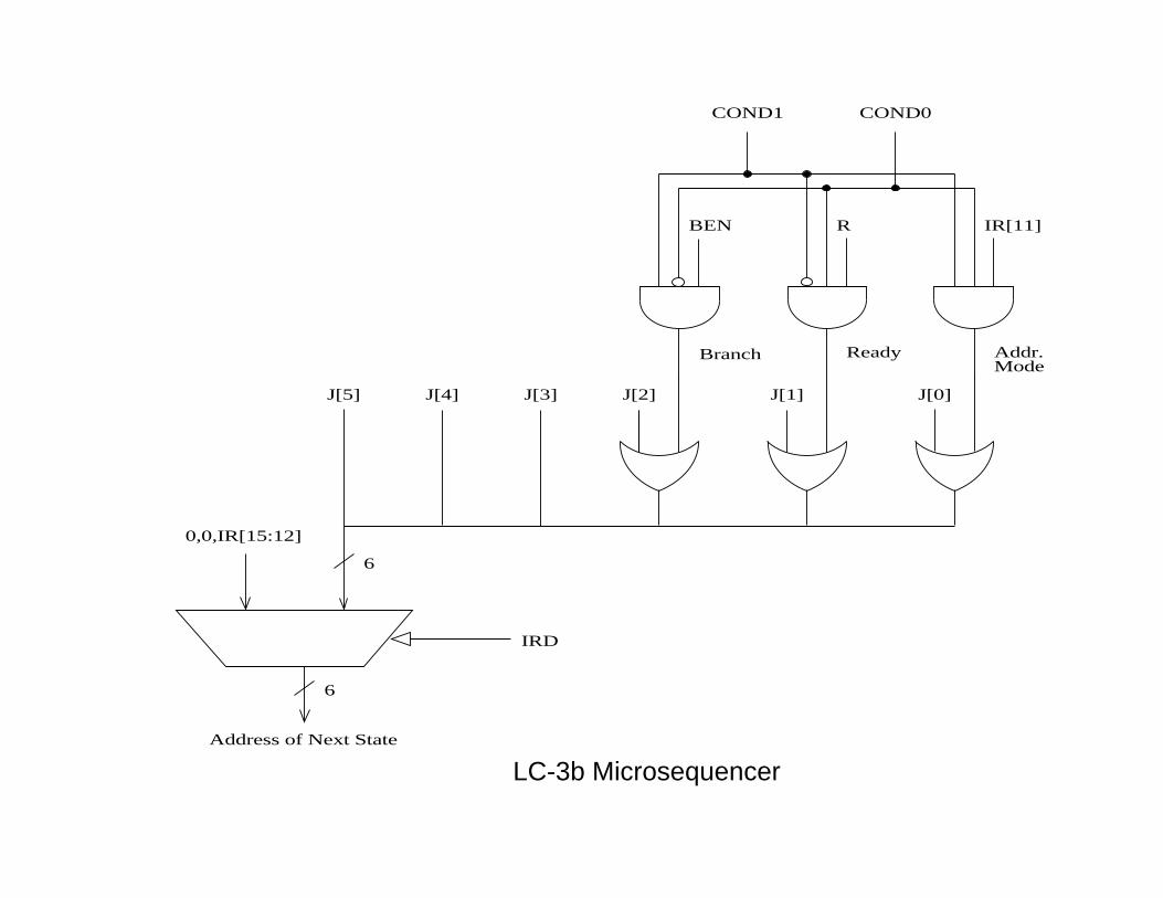
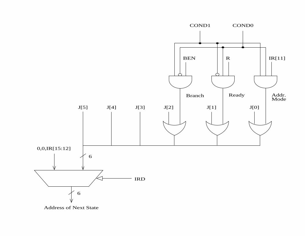
LC-3b Microsequencer Patt and Patel, Appendix C, Figure C.5
The purpose of the microsequencer is to determine the address of the next microinstruction (i.e., next state)
Next address depends on 9 control signals (plus 7 data signals)
35
IRD
Address of Next State
6
6
0,0,IR[15:12]
J[5]
Branch ReadyModeAddr.
J[0]J[1]J[2]
COND0COND1
J[3]J[4]
R IR[11]BEN
The Microsequencer: Some Questions When is the IRD signal asserted?
What happens if an illegal instruction is decoded?
What are condition (COND) bits for?
How is variable latency memory handled?
How do you do the state encoding? Minimize number of state variables (~ control store size) Start with the 16-way branch Then determine constraint tables and states dependent on COND
37
An Exercise in Microprogramming
38
IRD
Address of Next State
6
6
0,0,IR[15:12]
J[5]
Branch ReadyModeAddr.
J[0]J[1]J[2]
COND0COND1
J[3]J[4]
R IR[11]BEN
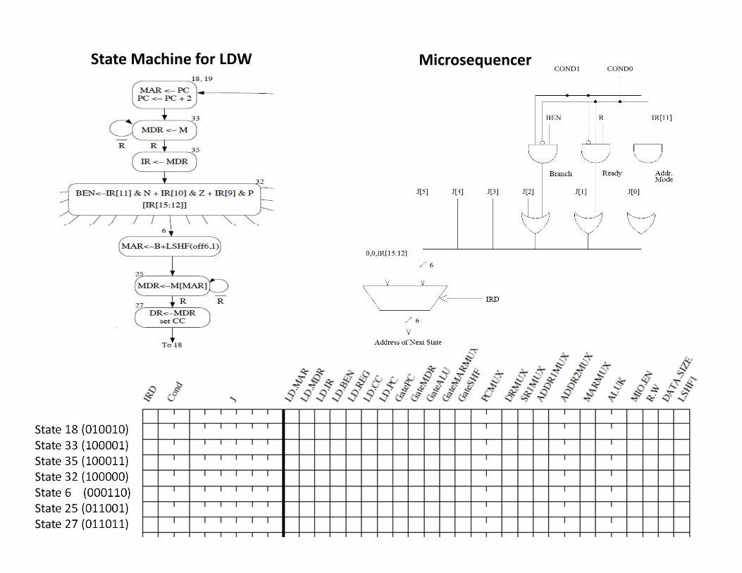
State 18 (010010)State 33 (100001)State 35 (100011)State 32 (100000)State 6 (000110)State 25 (011001)State 27 (011011)
State Machine for LDW Microsequencer

End of the Exercise in Microprogramming
40
The Control Store: Some Questions What control signals can be stored in the control store?
vs.
What control signals have to be generated in hardwired logic? i.e., what signal cannot be available without processing in the
datapath?
Remember the MIPS datapath One PCSrc signal depends on processing that happens in the
datapath (bcond logic)
41

Variable-Latency Memory The ready signal (R) enables memory read/write to execute
correctly Example: transition from state 33 to state 35 is controlled by
the R bit asserted by memory when memory data is available
Could we have done this in a single-cycle microarchitecture?
42
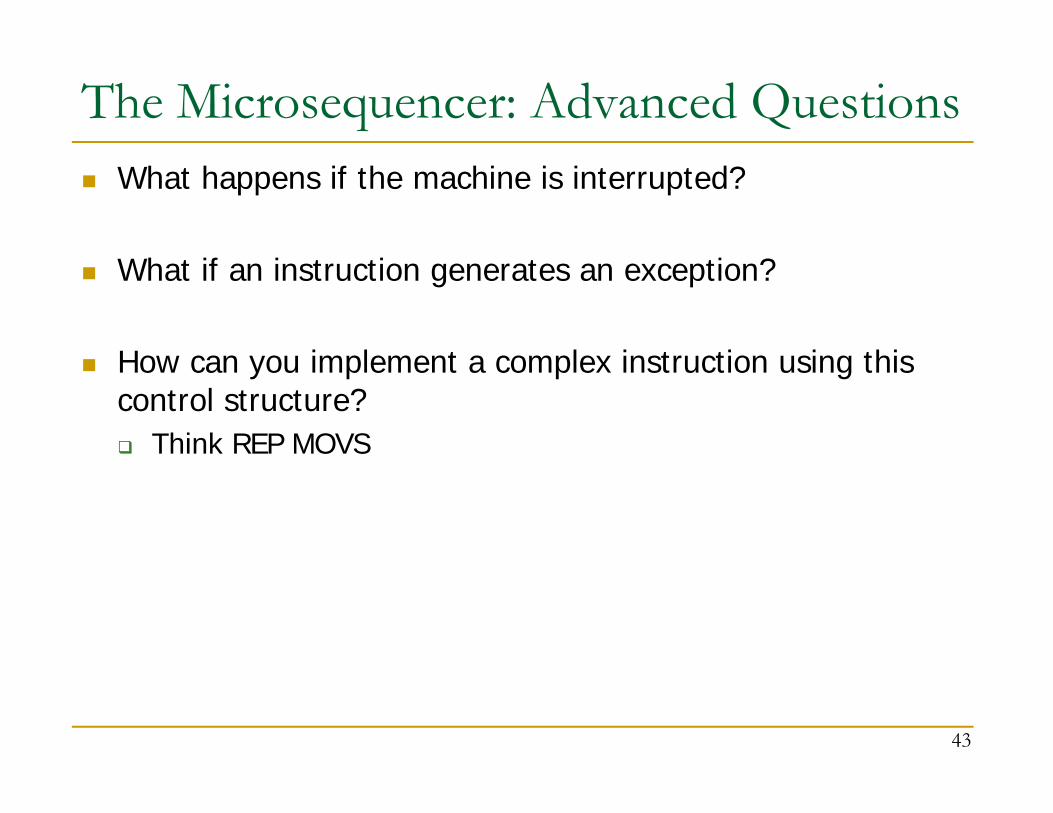
The Microsequencer: Advanced Questions What happens if the machine is interrupted?
What if an instruction generates an exception?
How can you implement a complex instruction using this control structure? Think REP MOVS
43

Advantages of Microprogrammed Control Allows a very simple design to do powerful computation by
controlling the datapath (using a sequencer) High-level ISA translated into microcode (sequence of microinstructions) Microcode (ucode) enables a minimal datapath to emulate an ISA Microinstructions can be thought of as a user-invisible ISA (micro ISA)
Enables easy extensibility of the ISA Can support a new instruction by changing the microcode Can support complex instructions as a sequence of simple microinstructions
If I can sequence an arbitrary instruction then I can sequence an arbitrary “program” as a microprogram sequence will need some new state (e.g. loop counters) in the microcode for sequencing
more elaborate programs
44
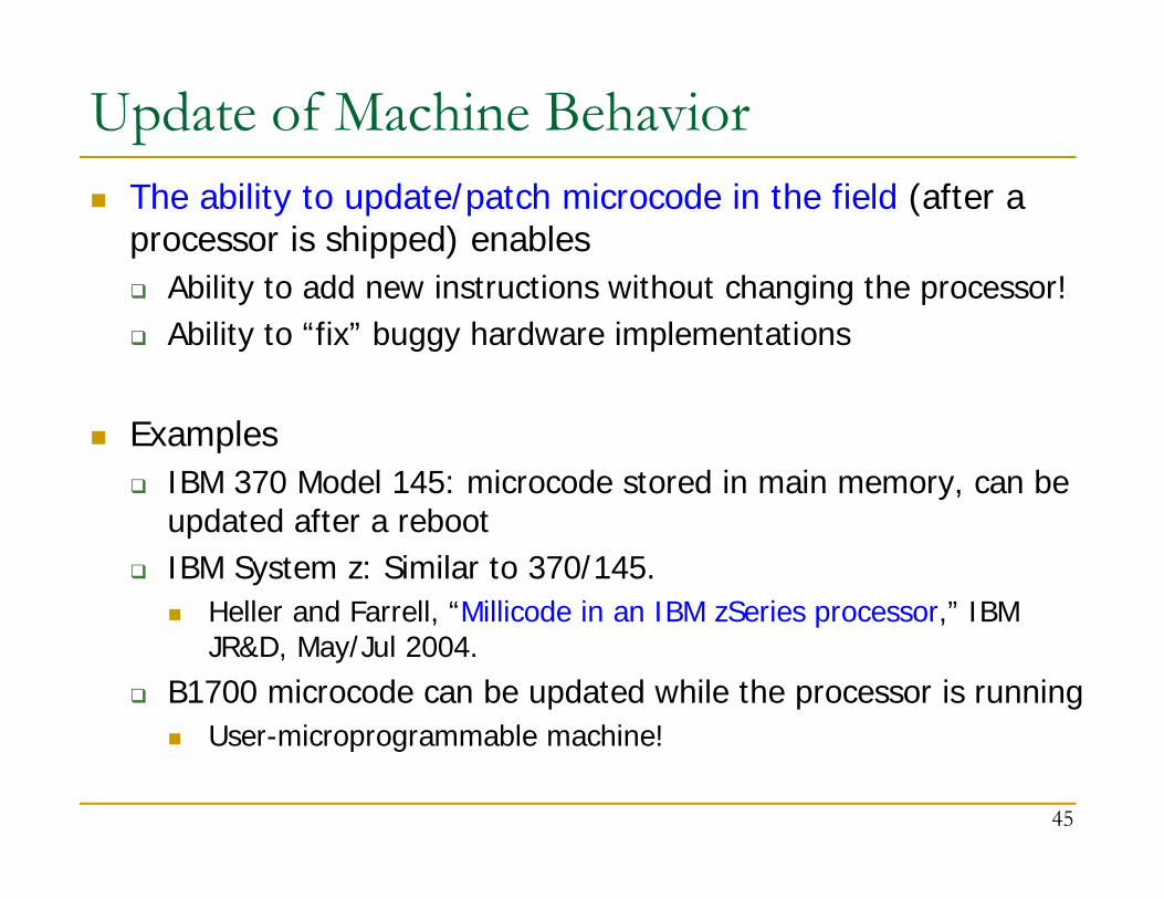
Update of Machine Behavior The ability to update/patch microcode in the field (after a
processor is shipped) enables Ability to add new instructions without changing the processor! Ability to “fix” buggy hardware implementations
Examples IBM 370 Model 145: microcode stored in main memory, can be
updated after a reboot IBM System z: Similar to 370/145.
Heller and Farrell, “Millicode in an IBM zSeries processor,” IBM JR&D, May/Jul 2004.
B1700 microcode can be updated while the processor is running User-microprogrammable machine!
45
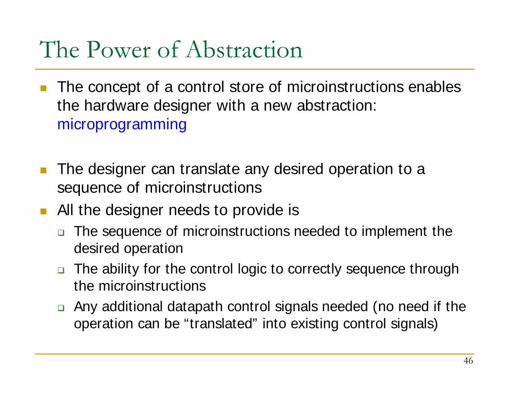
The Power of Abstraction The concept of a control store of microinstructions enables
the hardware designer with a new abstraction: microprogramming
The designer can translate any desired operation to a sequence of microinstructions
All the designer needs to provide is The sequence of microinstructions needed to implement the
desired operation The ability for the control logic to correctly sequence through
the microinstructions Any additional datapath control signals needed (no need if the
operation can be “translated” into existing control signals)
46
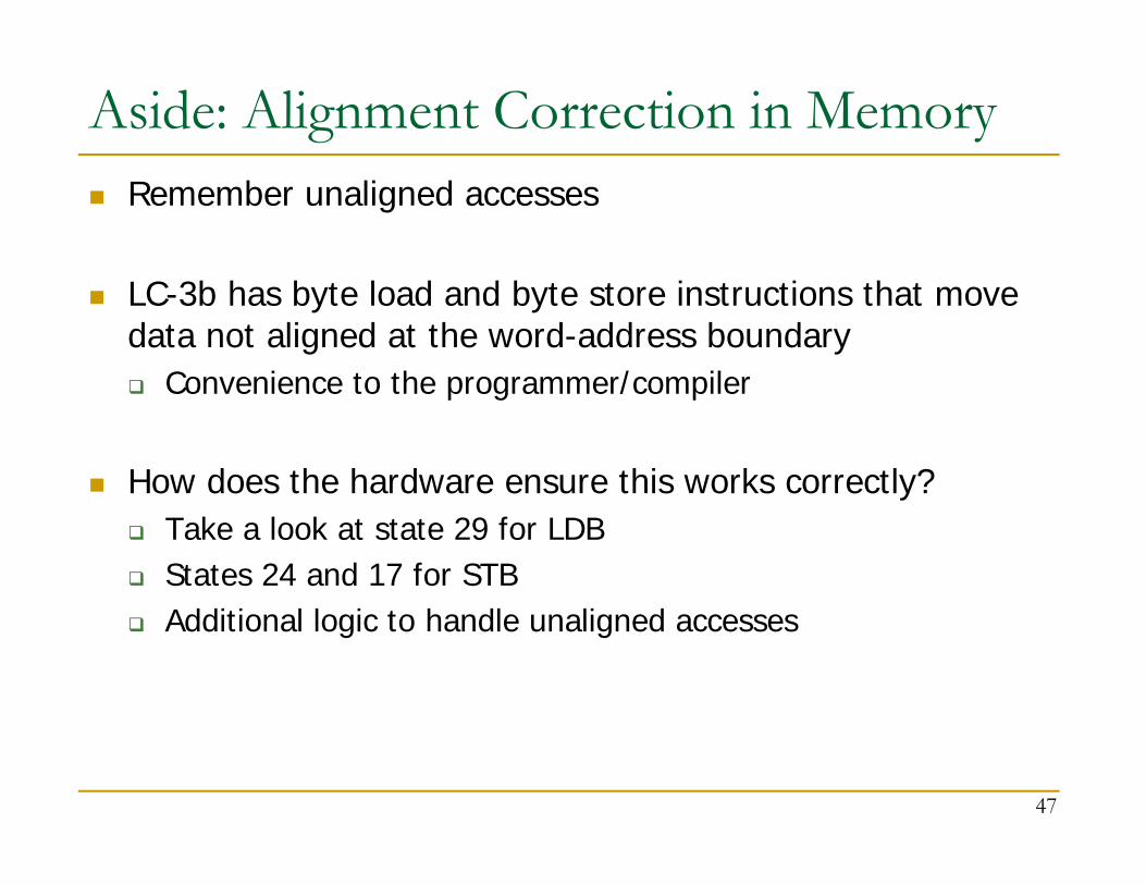
Aside: Alignment Correction in Memory Remember unaligned accesses
LC-3b has byte load and byte store instructions that move data not aligned at the word-address boundary Convenience to the programmer/compiler
How does the hardware ensure this works correctly? Take a look at state 29 for LDB States 24 and 17 for STB Additional logic to handle unaligned accesses
47
Aside: Memory Mapped I/O Address control logic determines whether the specified
address of LDx and STx are to memory or I/O devices
Correspondingly enables memory or I/O devices and sets up muxes
Another instance where the final control signals (e.g., MEM.EN or INMUX/2) cannot be stored in the control store These signals are dependent on address
48