Embed Size (px)
Citation preview

Computer Design
Computer Laboratory
Part Ib in Computer Science
Copyright c© Simon Moore, University of Cambridge, Computer Laboratory, 2011
Contents:
• 17 lectures of the Computer Design course
• Paper on Chuck Thacker’s Tiny Computer 3
• White paper on networks-on-chip for FPGAs
• Exercises for supervisions and personal study
• SystemVerilog “cheat” sheet which briefly coversmuch of what was learnt using the Cam-bridge SystemVerilog web tutor
Historic note: this course has had many guises. Until last year the course was in two parts:ECAD and Computer Design. Past paper questions on ECAD are still mostly relevant thoughthere has been a steady move toward SystemVerilog rather than Verilog 2001. This year theECAD+Arch labs have been completely rewritten for the new tPad hardware and making useof Chuck Thacker’s Tiny Computer 3 (TTC). The TTC is being used instead of our Tiger MIPScore since it is simple enough to be easily altered/upgraded as a lab. exercise. As a conse-quence some of the MIPS material has been removed in favour of a broader introduction toRISC processors; and the Manchester Baby Machine in SystemVerilog has been replaced byan introduction to the TTC and its SystemVerilog implementation. A new lecture on system’sdesign on FPGA using Altera’s Qsys tool has been added.
Lecture 1— Introduction and Motivation 1
Computer Design — Lecture 1
Introduction and Motivation y 1
Overview of the courseHow to build a computer:
4 × lectures introducing Electronic Computer Aided Design (ECAD) andthe Verilog/SystemVerilog language
Cambridge SystemVerilog web tutor (home work + 1 lab. sessionequivalent to 4 lectures worth of material)
7 × ECAD+Architecture Labs
14 × lectures on computer architecture and implementation
Contents of this lectureAims and Objectives
Implementation technologies
Technology trends
The hardware design gap
Recommended books and web material y 2
Recommended book (both ECAD and computer architecture):
D.M. Harris & S.L. Harris. Digital Design and Computer Architecture,Morgan Kaufmann 2007
General Computer Architecture:
J.L. Hennessey and D.A. Patterson, “Computer Architecture — AQuantitative Approach”, Morgan Kaufmann, 2002 (1996 edition alsogood, 1990 edition is only slightly out of date, 2006 edition good butcompacted down)
D.A. Patterson and J.L. Hennessey, “Computer Organization &Design — The Hardware/Software Interface”, Morgan Kaufmann,1998 (1994 version is also good, 2007 version now available)
Web:
http://www.cl.cam.ac.uk/Teaching/current/CompDesign/
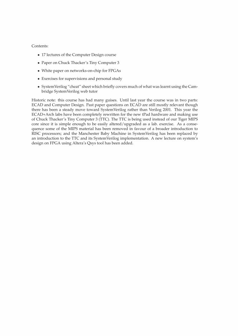
Revising State Machines y 3
Start with a state transition graph
i.e. it is a 2-bit counter with enable (go) input
Revising State Machines y 4
Then produce the state transition tablecurrent next
input state statego n1 n0 n1’ n0’0 0 0 0 00 0 1 0 10 1 0 1 00 1 1 1 11 0 0 0 11 0 1 1 01 1 0 1 11 1 1 0 0
Revising State Machines y 5
Then do Boolean minimisation, e.g. using K-maps
n0′ = n0⊕ go n1′ = go.n1 + n0.n1 + n0.n1.gon1′ = go.(n0⊕ n1) + go.n1
Revising State Machines y 6
And the final circuit diagram
now implement...
Revising PLAs y 7
PLA = programmable logic array
advantages — cheap (cost per chip) and simple to use
disadvantages — medium to low density integrated devices (i.e. not manygates per chip) so cost per gate is high
Field Programmable Gate Arrays y 8
a sea of logic elements made from small SRAM blocks
e.g. a 16×1 block of SRAM to provide any boolean function of 4variables
often a D-latch per logic element
programmable interconnect
program bits enable/disable tristate buffers and transmission gates
advantages: rapid prototyping, cost effective in low to medium volume
disadvantages: 15× to 25× bigger and slower than full custom CMOSASICs
2 Computer Design
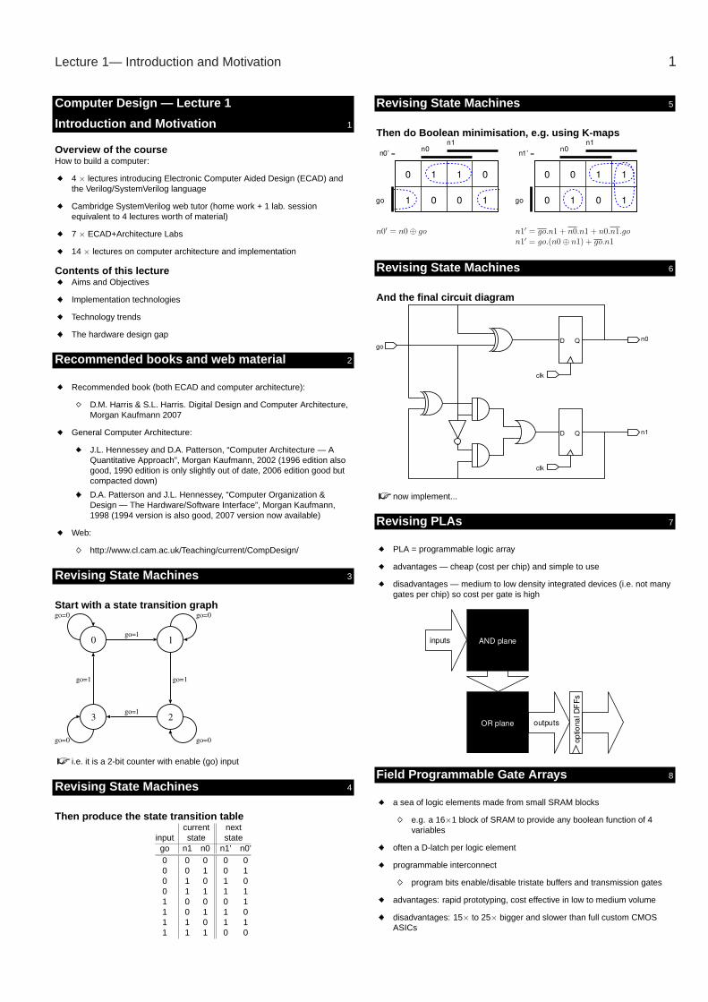
CMOS ASICsy 9
CMOS = complementary metal oxide semiconductor
ASIC = application specific integrated circuit
full control over the chip design
some blocks might be full custom
i.e. laid out by hand
other blocks might be standard cell
cells (gates, flip-flops, etc) are designed by hand but with inputs andoutputs in a standard configuration
designs are synthesised to a collection of standard cells...
...then a place & route tool arranges the cells and wires them up
blocks may also be generated by a macro
typically used to produce regular structures which need to be packedtogether carefully, e.g. a memory block
this material is covered in far more detail in the Part II VLSI course
Example CMOS chip y 10
very small and simple test chip from mid 1990s
see interactive version at:
http://www.cl.cam.ac.uk/users/swm11/testchip/
Zooming in on CMOS chip (1) y 11
Zooming in on CMOS chip (2) y 12
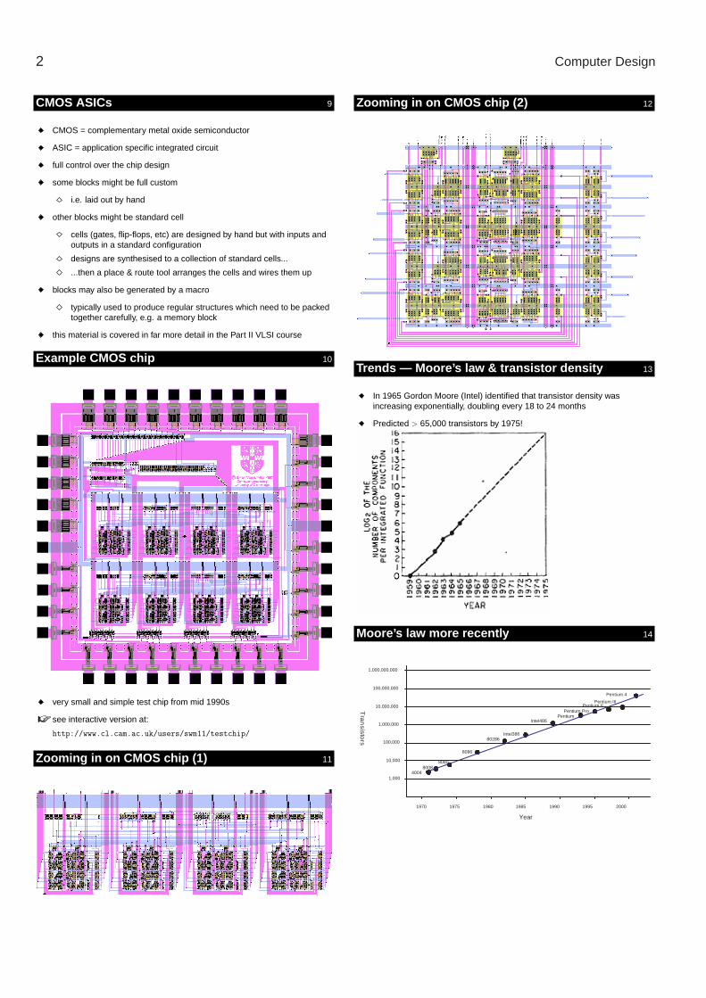
Trends — Moore’s law & transistor density y 13
In 1965 Gordon Moore (Intel) identified that transistor density wasincreasing exponentially, doubling every 18 to 24 months
Predicted > 65,000 transistors by 1975!
Moore’s law more recently y 14
Year
T r a n s i s t o r s
4004 8008
8080
8086
80286 Intel386
Intel486 Pentium
Pentium Pro Pentium II
Pentium III
Pentium 4
1,000
10,000
100,000
1,000,000
10,000,000
100,000,000
1,000,000,000
1970 1975 1980 1985 1990 1995 2000
Lecture 1— Introduction and Motivation 3
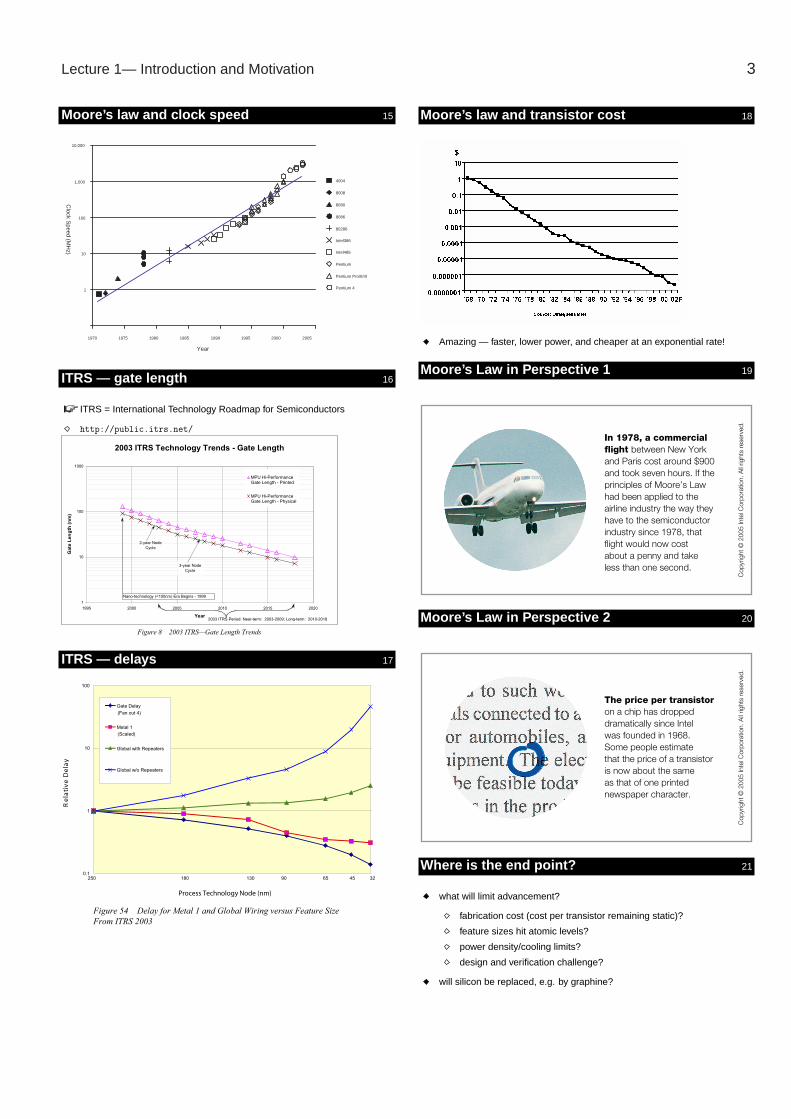
Moore’s law and clock speed y 15
Year
1
10
100
1,000
10,000
1970 1975 1980 1985 1990 1995 2000 2005
4004
8008
8080
8086
80286
Intel386
Intel486
Pentium
Pentium Pro/II/III
Pentium 4
Clock S
peed (MH
z)
ITRS — gate length y 16
ITRS = International Technology Roadmap for Semiconductors
http://public.itrs.net/
Figure 8 2003 ITRS—Gate Length Trends
2003 ITRS Technology Trends - Gate Length
1
10
100
1000
1995 2000 2005 2010 2015 2020
Year
)m
n( ht
gn
eL
eta
G
MPU Hi-PerformanceGate Length - Printed
MPU Hi-PerformanceGate Length - Physical
Nano-technology (<100nm) Era Begins - 1999
2003 ITRS Period: Near-term: 2003-2009; Long-term: 2010-2018
2-year Node
Cycle
3-year Node
Cycle
ITRS — delays y 17
Figure 54 Delay for Metal 1 and Global Wiring versus Feature Size
From ITRS 2003
0.1
1
10
100
Process Technology Node (nm)
yal
eD
evit
ale
R
Gate Delay
Metal 1
Global with Repeaters(Scaled Die Edge)
Global w/o Repeaters(Scaled Die Edge)
250 180 130 90 65 45
(Fan out 4)
(Scaled)
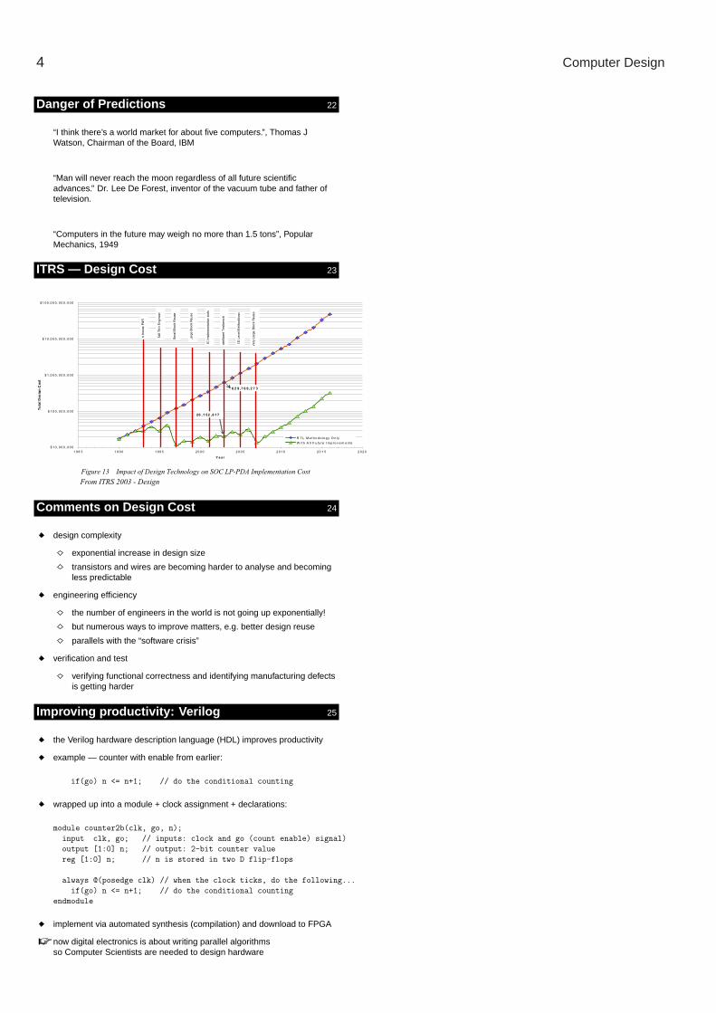
32
Moore’s law and transistor cost y 18
Amazing — faster, lower power, and cheaper at an exponential rate!
Moore’s Law in Perspective 1 y 19
Moore’s Law in Perspective 2 y 20
Where is the end point? y 21
what will limit advancement?
fabrication cost (cost per transistor remaining static)?
feature sizes hit atomic levels?
power density/cooling limits?
design and verification challenge?
will silicon be replaced, e.g. by graphine?
4 Computer Design
Danger of Predictions y 22
“I think there’s a world market for about five computers.”, Thomas JWatson, Chairman of the Board, IBM
“Man will never reach the moon regardless of all future scientificadvances.” Dr. Lee De Forest, inventor of the vacuum tube and father oftelevision.
“Computers in the future may weigh no more than 1.5 tons”, PopularMechanics, 1949
ITRS — Design Cost y 23
Figure 13 Impact of Design Technology on SOC LP-PDA Implementation Cost
$ 1 0 , 0 0 0 , 0 0 0
$ 1 0 0 , 0 0 0 , 0 0 0
$ 1 ,0 0 0 , 0 0 0 , 0 0 0
$ 1 0 ,0 0 0 , 0 0 0 , 0 0 0
$ 1 0 0 ,0 0 0 , 0 0 0 , 0 0 0
1 9 8 5 1 9 9 0 1 9 9 5 2 0 0 0 2 0 0 5 2 0 1 0 2 0 1 5 2 0 2 0
Y e a r
R TL M e t h o d o lo g y O n ly
W it h A l l F u tu re I m p ro v e m e n ts
re
eni
gn
E ni
hT ll
aT
esu
eR
kc
olB ll
am
S
slo
ot n
oitat
ne
mel
pmI
CI
es
ue
R kc
olB
egr
aL
hc
ne
btse
T tn
egill
etnI
yg
olo
do
hte
M le
ve
L S
E
es
ue
R kc
olB
egr
aL
yre
V
6 2 9 ,7 6 9,2 7 3
20 ,1 52 ,6 17
ts
oC
ngi
se
D lat
oT
R&
P es
uo
h nI
From ITRS 2003 - Design
Comments on Design Cost y 24
design complexity
exponential increase in design size
transistors and wires are becoming harder to analyse and becomingless predictable
engineering efficiency
the number of engineers in the world is not going up exponentially!
but numerous ways to improve matters, e.g. better design reuse
parallels with the “software crisis”
verification and test
verifying functional correctness and identifying manufacturing defectsis getting harder
Improving productivity: Verilog y 25
the Verilog hardware description language (HDL) improves productivity
example — counter with enable from earlier:
if(go) n <= n+1; // do the conditional counting
wrapped up into a module + clock assignment + declarations:
module counter2b(clk, go, n);
input clk, go; // inputs: clock and go (count enable) signal)
output [1:0] n; // output: 2-bit counter value
reg [1:0] n; // n is stored in two D flip-flops
always @(posedge clk) // when the clock ticks, do the following...
if(go) n <= n+1; // do the conditional counting
endmodule
implement via automated synthesis (compilation) and download to FPGA
now digital electronics is about writing parallel algorithmsso Computer Scientists are needed to design hardware

Lecture 2 — Logic modelling, simulation and synthesis 5
Computer Design — Lecture 2
Logic Modeling, Simulation and Synthesis y 1
Lectures so farthe last lecture looked at technology and design challenges
Overview of this lecturethis lecture introduces:
modeling
simulation techniques
synthesis techniques for logic minimisation and finite state machine (FSM)optimisation
Four valued logic y 2
value meaning0 false1 truex undefinedz high impedance
AND 0 1 x z0 0 0 0 01 0 1 x xx 0 x x xz 0 x x x
OR 0 1 x z0 0 1 x x1 1 1 1 1x x 1 x xz x 1 x x
NOT output0 11 0x xz x
BUFT enabledata 0 1 x z
0 z 0 x x1 z 1 x xx z x x xz z x x x
Modeling a tri-state buffer y 3
module BUFT(
output reg out,
input in,
input enable);
// behavioural use of always which activates whenever
// enable or in changes (i.e. both positive and negative edges)
always @(enable or in)
if(enable)
out = in;
else
out = 1’bz; // assign high-impedance
endmodule
Such models are useful for simulation purposes but cannot usually besynthesised. Rather, such a model would have to be replaced by apredefined cell/component.
Verilog and logic levels y 4
’z’ can be used to indicate tri-state (see previous example)
’===’ can be used to compare wires to see if they are tri-state
similarly, !== is to === what != is to ==
these operators are only useful for simulation (not supported for synthesis)
during simulation x and z are treated as false for conditional expressions
== 0 1 x z0 1 0 x x1 0 1 x xx x x x xz x x x x
=== 0 1 x z0 1 0 0 01 0 1 0 0x 0 0 1 0z 0 0 0 1
Verilog casex and casez statements y 5
casez — z values are considered to be “don’t care”
casex — z and x values are considered to be “don’t care”
example:
reg [3:0] r;
casex(r)
4’b000x : statement1;
4’b10x1 : statement2;
4’b1x11 : statement3;
endcase
some values of r the outcome4’b0001 matches statement 14’b0000 matches statement 14’b000x matches statement 14’b000z matches statement 14’b1001 matches statement 24’b1111 matches statement 3
Problems when modeling a tristate bus y 6
scenario:
start: dataA=dataB=enableB=0 and enableA=1step 1: enableA-step 2: enableB+
? what is that state of the bus between steps 1 and 2? 0 or z?
? should the output ever go to x and what might the implications be if itdoes?
Further logic levels y 7
to simulate charge holding elements (capacitors) we could introduce twoadditional logic levels:
weak low — indicates that the capacitor has been discharged to lowbut is not being driven by anything
weak high — indicates that the capacitor has been charged high butis not being driven by anything
further logic levels can be added to account for larger capacitances, riseand fall times, etc.
the standard VHDL (another HDL) logic library uses a 46 state logic calledt logic

6 Computer Design
Modeling delays y 8
adding delays to behavioural Verilog (typically for simulation only), e.g. todelay by 10 simulator time units:
assign #10 delayed_value = none_delayed_value;
pure delay — signals are delayed by some time constant
inertial delay — models capacitive delay
Obtaining delay information y 9
a design can be synthesised to gates and approximations of the gatedelays can be used
gates in the netlist can be placed and wires routed so that wire lengthsand capacitances can be determined
models of gates can vary
e.g. input to output delay depends upon which input is changing(even on trivial gates like a 2 input NOR) and this variation may bemodeled but often some simplifying assumption is made like takingthe average case
back annotation
delay information can be back annotated, e.g. adding hiddeninformation to a schematic diagram
delay information and netlist can be converted back into a low levelstructural Verilog model
Naıve simulation y 10
simplifying assumptions for our naıve simulation:
each gate has unit delay (1 virtual time unit)
netlist held as a simple list of gates with enumerated wires to indicateinterconnect
an array of wires holds the state
simulation takes the current state (wire information) and evaluates eachgate to in turn to produce a new set of state. This process is thenrepeated.
problems:
many parts of the circuit are likely to be inactive at a given instant intime, so having to reevaluate each gate for every simulation cycle isexpensive
delays have to be implemented as long strings of buffers which islikely to slow things down
Introduction to discrete event simulation y 11
sometimes called Delta simulation
only changes in state cause gates to be reevaluated
data structures:
gates are modeled as objects (including current state information)
state changes passed as (virtual) timed events or messages
pending events are inserted into a time ordered event queue
simulation loops around:
pick event with least virtual time off the event queue
pass event to appropriate gate
gate evaluates and produces an event if its output has changed
issues:
cancelling runt pulses (event removal)
modeling wire delays (add wires as simple gates)
SPICEy 12
SPICE = Simulation Program with Integrated Circuit Emphasis
used for detailed analog transistor level simulation
models nonlinear components as a set of differential equationsrepresenting the circuit voltages, currents and resistances
simulation is highly accurate (accuracy dependent upon models provided)
but simulation is computationally expensive and only practical for smallcircuits
sometimes SPICE is used to analyse standard cells in order to determinetypical delays, etc, to enable reasonably accurate digital simulation to beundertaken
there are various versions of commercial and free SPICE which vary inperformance and accuracy depending on implementation details
Synthesis — Design metrics y 13
many digital logic circuits achieve the same function, but vary in the:
number of gates
total wiring length
timing properties through various paths
power consumption
Karnaugh maps and Boolean n-cubes y 14
implicants are sub n-cubes

Lecture 2 — Logic modelling, simulation and synthesis 7
Quine-McCluskey minimisation — step 1 y 15
find all prime implicants using x.y + x.y = x repeatedly
first produce a truth table for the function and extract the mintermsrequired (i.e. rows in the truth table where the output is 1)
exhaustively compare pairs of terms which differ by 1 bit to produce anew term where the 1 bit difference is marked by a don’t care X
tick those terms which have been selected since they are covered bythe new term
repeat with new set of terms (X must match X) until no more termscan be produced
terms which are unticked are the prime implicants
Quine-McCluskey minimisation — step 2 y 16
select smallest set of prime implicants to cover function:
prepare prime-implicants chart
select essential prime implicants for which one or more of itsminterms are unique (only once in the column)
obtain a new reduced PI chart for remaining prime-implicants and theremaining minterms
select one or more of remaining prime implicants which will cover allthe remaining minterms
computationally very expensive for large equations
tools like Espresso use heuristics to improve performance but at theexpense of not being exact
there are better but far more complex algorithms for exact Booleanminimisation
QM example y 17
An example truth tableCode ABCD Term Output
0 0000 ABCD 01 0001 ABCD 02 0010 ABCD 03 0011 ABCD 04 0100 ABCD 05 0101 ABCD 16 0110 ABCD 07 0111 ABCD 08 1000 ABCD 09 1001 ABCD 010 1010 ABCD 111 1011 ABCD 112 1100 ABCD 013 1101 ABCD 114 1110 ABCD 115 1111 ABCD 1
QM example cont... y 18
The active mintermsCode ABCD
5 010110 101011 101113 110114 111015 1111
QM example cont... y 19
Find terms which differ by one bitCode ABCD Notes
5 0101 X
10 1010 X
11 1011 X
13 1101 X
14 1110 X
15 1111 X
New terms:A X101 combining 5,13B 101X combining 10,11C 1X10 combining 10,14D 1X11 combining 11,15E 11X1 combining 13,15F 111X combining 14,15
where X indicates that a term is covered
QM example cont... y 20
Find terms which differ by one bit and have X’s in the sameplaceCode ABCD Notes
A X101B 101X X
C 1X10 X
D 1X11 X
E 11X1F 111X X
New terms:G 1X1X combining B,FH 1X1X combining C,D — duplicate so remove
QM example cont... y 21
The prime implicant chartactive minterms terms
Code ABCD A: X101 E: 11X1 G: 1X1X5 0101 X
10 1010 X
11 1011 X
13 1101 X X
14 1110 X
15 1111 X X
where X indicates that a term covers a minterm
so terms A and G cover all minterms (i.e. they are essential terms) andterm E is not required
therefore the minimised equation is B.C.D + A.C
Further comments on logic minimisation y 22
if optimising over multiple equations (i.e. multiple outputs) with sharedterms then the Putnam and Davis algorithm can be used (but not muchmore sophisticated than QM)
sum of products form may not be simplest logic structure: multi-level logicstructures are often more compact (ongoing research in this area)
sometimes simplification in terms of XOR gates (rather than AND and ORgates) is more appropriate — called Read-Muller logic
e.g. see “Hug an XOR gate today: an introduction to Read-Muller logic”:
http://www.reed-electronics.com/ednmag/archives/1996/030196/05df4.htm
don’t-cares are very important for efficient logic minimisation so whenwriting Verilog it is important to indicate undefined values, e.g.:
wire [31:0] my_alu = (opcode==’add) ? a + b :
(opcode==’not) ? ~a :
(opcode==’sub) ? a - b : 32’bx;

8 Computer Design
Adding redundant logic y 23
adding redundant logic can reduce the amount of wiring required
Wire minimisation y 24
wire minimisation is largely the job of the place & route tool and not thesynthesis tool
the synthesis tools may include:
redundant logic
placement hints to guide place & route
manual floor planning may also be performed to force the hand of theplace & route tools
increasingly important as chips get larger
Finite state machine minimisation y 25
state minimisation
remove duplicate states
remove redundant/unreachable states
state assignment
assign a unique binary code to each state
the logic structure depends on the assignment, thus this needs to bedone optimally (e.g. algorithms: NOVA, JEDI)
BUT much Verilog code is explicit about register usage so littleoptimisation possible
higher level behavioral Verilog introduces implicit state machineswhich the synthesis tool is in a better position to optimise
Retiming and D-latch migration y 26
if a path through some logic is too long then it is sometimes possible tomove the flip-flops to compensate without altering the functional behaviour
similarly, it is sometimes possible to add extra D-latches to make apipeline longer

Lecture 3 — Chip, board and system testing 9
Computer Design — Lecture 3
Testing y 1
Overview of this lectureIntroduce:
production test (fault models, test metrics, test pattern generation, scanpath testing)
functional test (in simulation and on FPGA)
introduction to ECAD lab sessions
Objectives of production testing y 2
check that there are no manufacturing defects
NOT to check whether you have designed the device correctly
economics: cost of detecting a faulty component is lowest before it ispackaged and embedded in a system
for consumer products:
faulty goods cost a lot to replace so require low defect rate (e.g. lessthat 0.1%)
but testing costs money so don’t exhaustively test — 98% faultcoverage probably acceptable
for medical, aerospace and military (i.e. safety-critical) products:
must have 100% coverage
in some instances a design will contain redundant units (e.g. on DRAM)which can be selected, thereby improving yield
Fault models y 3
logical faults
stuck-at (most common)
CMOS stuck-open
CMOS stuck-on
bridging faults
parametric faults
low/high voltage/current levels
gate or path delay-faults
testing methods:
parametric (electrical) tests also detect stuck-on faults
logical tests detect stuck-at faults
transition tests detect stuck-open faults
timed transition tests detect delay faults
Testability y 4
controllability
the ability to set and clear internal signals
it is particularly useful to be able to change the state in registersinside a circuit
observability
the ability to detect internal signals
Fault reductions y 5
checkpoints
points where faults could occur
fault equivalence
remove test for least significant fault
fault dominance
if every test for fault f1 detects f2 then f1 dominates f2
⇒ only have to generate test for f1
Test patterns and path sensitisation y 6
test patterns are sequences of (input values, expected result) pairs
path sensitisation
inputs required in order to make a fault visible on the outputs
Test effectiveness y 7
undetectable fault — no test exists for fault
redundant fault — undetectable fault whose occurrence does not affectcircuit operation
testability = number of detectable faultsnumber of faults
effective faults = number of faults − redundant faults
fault coverage = number of detectable faultsnumber of effective faults
test set size = number of test patterns
goal is 100% fault coverage (not 100% testability) with a minimum sizedtest set
10 Computer Design
Automatic Test Pattern Generation (ATPG) y 8
Many algorithms developed to do ATPG, e.g. D-Algorithm, PODEM,PODEM-X, etc.General idea:
generate a sequence of test vectors to identify faults
test vector = 〈input vector, correct output vector〉
input and output vectors are typically 3 valued: (0, 1, X)
simple combinatoric circuits (no feedback) can be supplied with testvectors in any order
circuits with memory (latches/combinatoric feedback) require sequencesof test vectors in order to modify internal state, e.g. consider having to test:
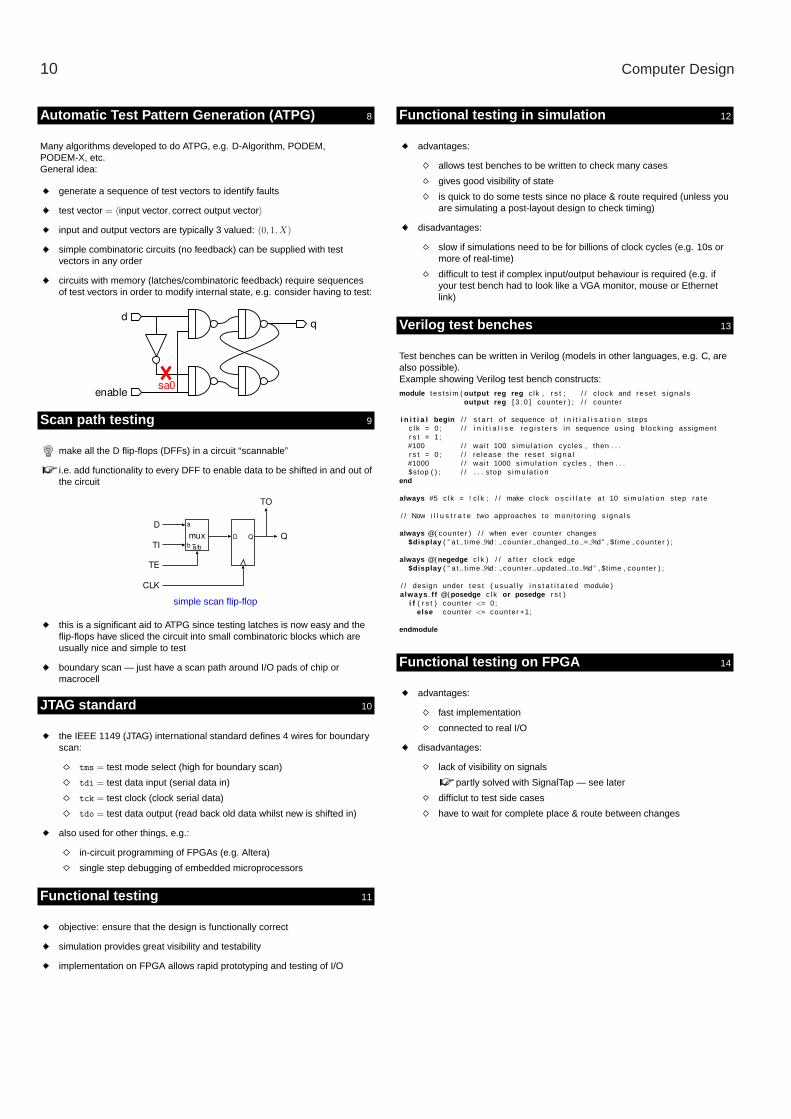
Scan path testing y 9
make all the D flip-flops (DFFs) in a circuit “scannable”
i.e. add functionality to every DFF to enable data to be shifted in and out ofthe circuit
simple scan flip-flop
this is a significant aid to ATPG since testing latches is now easy and theflip-flops have sliced the circuit into small combinatoric blocks which areusually nice and simple to test
boundary scan — just have a scan path around I/O pads of chip ormacrocell
JTAG standard y 10
the IEEE 1149 (JTAG) international standard defines 4 wires for boundaryscan:
tms = test mode select (high for boundary scan)
tdi = test data input (serial data in)
tck = test clock (clock serial data)
tdo = test data output (read back old data whilst new is shifted in)
also used for other things, e.g.:
in-circuit programming of FPGAs (e.g. Altera)
single step debugging of embedded microprocessors
Functional testing y 11
objective: ensure that the design is functionally correct
simulation provides great visibility and testability
implementation on FPGA allows rapid prototyping and testing of I/O
Functional testing in simulation y 12
advantages:
allows test benches to be written to check many cases
gives good visibility of state
is quick to do some tests since no place & route required (unless youare simulating a post-layout design to check timing)
disadvantages:
slow if simulations need to be for billions of clock cycles (e.g. 10s ormore of real-time)
difficult to test if complex input/output behaviour is required (e.g. ifyour test bench had to look like a VGA monitor, mouse or Ethernetlink)
Verilog test benches y 13
Test benches can be written in Verilog (models in other languages, e.g. C, arealso possible).Example showing Verilog test bench constructs:module t es ts im ( output reg reg c lk , r s t ; / / c lock and rese t s i gna l s
output reg [ 3 : 0 ] counter ) ; / / counter
i n i t i a l begin / / s t a r t o f sequence of i n i t i a l i s a t i o n stepsc l k = 0 ; / / i n i t i a l i s e r e g i s t e r s i n sequence using b lock ing assigmentr s t = 1 ;#100 / / wa i t 100 s imu la t i on cycles , then . . .r s t = 0 ; / / re lease the rese t s i g n a l#1000 / / wa i t 1000 s imu la t i on cycles , then . . .$stop ( ) ; / / . . . s top s imu la t i on
end
always #5 c l k = ! c l k ; / / make c lock o s c i l l a t e a t 10 s imu la t i on step ra te
/ / Now i l l u s t r a t e two approaches to mon i to r ing s igna l s
always @( counter ) / / when ever counter changes$display ( ” a t t ime %d : counter changed to = %d ” , $time , counter ) ;
always @( negedge c l k ) / / a f t e r c lock edge$display ( ” a t t ime %d : counter updated to %d ” , $time , counter ) ;
/ / design under t e s t ( usua l l y i n s t a t i t a t e d module )always f f @( posedge c l k or posedge r s t )
i f ( r s t ) counter <= 0;else counter <= counter +1;
endmodule
Functional testing on FPGA y 14
advantages:
fast implementation
connected to real I/O
disadvantages:
lack of visibility on signals
partly solved with SignalTap — see later
difficlut to test side cases
have to wait for complete place & route between changes

Lecture 3 — Chip, board and system testing 11
Key debouncer example y 15
module debounce ( input c lk , / / c lock a t 50MHzinput r s t , / / r ese tinput bouncy , / / bouncy s i g n a loutput reg clean , / / c lean s i g n a loutput reg [ 1 5 : 0 ] numbounces ) ;
reg prev syncbouncy ;reg [ 2 0 : 0 ] counter ;wire counterAtMax = &counter ; / / N.B . vec to r AND of the b i t swire syncbouncy ;synchron iser dosync ( . c l k ( c l k ) , . async ( bouncy ) , . sync ( syncbouncy ) ) ;always f f @( posedge c l k or posedge r s t )
i f ( r s t ) begincounter <= 0;numbounces <= 0;prev syncbouncy <= 0;clean <= 0;
end else beginprev syncbouncy <= syncbouncy ;i f ( syncbouncy != prev syncbouncy ) begin / / de tec t change
counter <= 0;numbounces <= numbounces+1;
end else i f ( ! counterAtMax ) / / no bouncing , so keep count ingcounter <= counter +1;
else / / ou tput c lean s i g n a l s ince inpu t s tab le f o r/ / 2ˆ21 c lock cyc les ( approx . 42ms)
clean <= syncbouncy ;end
endmodule
Synchroniser y 16
module synchron iser (input c lk ,input async ,output reg sync ) ;
reg metastable ;always @( posedge c l k ) begin
metastable <= async ;sync <= metastable ;
endendmodule
Test bench for key debouncer y 17
module testbench (output reg c lk ,output reg r s t ,output reg bouncy ,output clean ) ;
wire [ 1 5 : 0 ] numbounces ;
debounce DUT( . c l k ( c l k ) , . r s t ( r s t ) , . bouncy ( bouncy ) , . c lean ( clean ) ,. numbounces ( numbounces ) ) ;
i n i t i a l beginc l k =0;r s t =1;bouncy =0;
#100 r s t =0;#10000 bouncy =1; / / 1e3 t i c k s#10000 bouncy =0;#100000 bouncy =1; / / 1e4 t i c k s#100000 bouncy =0;#1000000 bouncy =1; / / 1e5 t i c k s#1000000 bouncy =0;#10000000 bouncy =1; / / 1e6 t i c k s#30000000 bouncy =0; / / 3e6 t i c k s ( should have gone high )#30000000 $stop ;
end
always #5 c l k = ! c l k ;
always @( r s t )$display ( ”%09d : r s t = %d ” , $time , r s t ) ;
always @( bouncy or clean or numbounces [ 1 5 : 0 ] )$display ( ”%09d : bouncy = %d clean = %d numbounces = %d ” ,
$time , bouncy , clean , numbounces ) ;
endmodule
Modelsim simulation output y 18
# 0: bouncy = 0 clean = x numbounces = x
# 0: rst = 1
# 0: bouncy = 0 clean = 0 numbounces = 0
# 100: rst = 0
# 10100: bouncy = 1 clean = 0 numbounces = 0
# 10125: bouncy = 1 clean = 0 numbounces = 1
# 20100: bouncy = 0 clean = 0 numbounces = 1
# 20125: bouncy = 0 clean = 0 numbounces = 2
# 120100: bouncy = 1 clean = 0 numbounces = 2
# 120125: bouncy = 1 clean = 0 numbounces = 3
# 220100: bouncy = 0 clean = 0 numbounces = 3
# 220125: bouncy = 0 clean = 0 numbounces = 4
# 1220100: bouncy = 1 clean = 0 numbounces = 4
# 1220125: bouncy = 1 clean = 0 numbounces = 5
# 2220100: bouncy = 0 clean = 0 numbounces = 5
# 2220125: bouncy = 0 clean = 0 numbounces = 6
# 12220100: bouncy = 1 clean = 0 numbounces = 6
# 12220125: bouncy = 1 clean = 0 numbounces = 7
# 33191645: bouncy = 1 clean = 1 numbounces = 7
# 42220100: bouncy = 0 clean = 1 numbounces = 7
# 42220125: bouncy = 0 clean = 1 numbounces = 8
# 63191645: bouncy = 0 clean = 0 numbounces = 8
# Break in Module testbench at ...
On FPGA test y 19
module keybounce (input CLOCK 50 ,input [ 1 7 : 0 ] SW,input [ 3 : 0 ] KEY,output [ 1 7 : 0 ] LEDR,output [ 7 : 0 ] LEDG) ;
(∗ preserve , noprune ∗ ) reg [ 3 1 : 0 ] t imer ;(∗ preserve , noprune ∗ ) reg [ 2 : 0 ] d e l a y e d t r i g g e r c o n d i t i o n ;(∗ preserve , noprune ∗ ) reg bouncy ;(∗ keep , noprune ∗ ) wire r s t , c lean ;(∗ keep , noprune ∗ ) wire t r i g g e r c o n d i t i o n = SW[ 0 ] ˆ c lean ;(∗ keep , noprune ∗ ) wire [ 1 5 : 0 ] numbounces ;always @( posedge CLOCK 50) begin
bouncy <= SW[ 0 ] ;d e l a y e d t r i g g e r c o n d i t i o n <= { d e l a y e d t r i g g e r c o n d i t i o n [ 1 : 0 ] , t r i g g e r c o n d i t i o n } ;
endalways @( posedge CLOCK 50 or posedge r s t )
i f ( r s t ) t imer <=0; else t imer<=t imer +1;synchron iser sync rs t ( . c l k (CLOCK 50 ) , . async ( ! KEY [ 0 ] ) , . sync ( r s t ) ) ;debounce DUT( . c l k (CLOCK 50 ) , . r s t ( r s t ) , . bouncy ( bouncy ) , . c lean ( clean ) ,
. numbounces ( numbounces ) ) ;assign LEDG[ 1 : 0 ] = clean ? 2 ’ b11 : 2 ’ b00 ;assign LEDG[ 3 : 2 ] = SW[ 0 ] ? 2 ’ b11 : 2 ’ b00 ;assign LEDG[ 7 : 4 ] = { d e l a y e d t r i g g e r c o n d i t i o n [ 2 ] , bouncy , t r i g g e r c o n d i t i o n , t imer [ 3 1 ] } ;assign LEDR[ 1 7 : 0 ] = {2 ’b00 , numbounces [ 1 5 : 0 ] } ;
endmodule
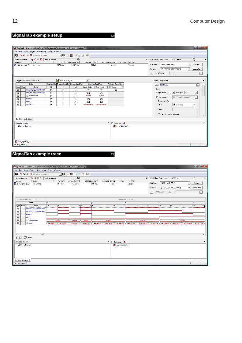
SignalTap y 20
motivation: provide analysis of state of running system
approach: automatically add extra hardware to capture signals of interest
SignalTap: Altera’s tool to make this easier
for further details see the Lab. web pages
SignalTap example y 21
probe the debouncer degin
difficulty: bounce events happen infrequently and there is not enoughmemory on the FPGA to store a long trace of events every clock cycle
solution: start and stop signal capture to observe the interesting bits(trigger signals added to the design to achieve this)
12 Computer Design
SignalTap example setup y 22
SignalTap example trace y 23

Lecture 4 — Verilog systems design 13
Computer Design — Lecture 4
Design for FPGAs y 1
Overview of this lecturethis lecture:
introduces the tPad FPGA board
gives some more SystemVerilog design examples
presents some design techniques
explains some design pitfalls
ECAD+Architecture lab. teaching boards (tPads) y 2
Front of the tPad y 3
FPGA design flow y 4
Lab 1 shows you how to use the following key components of Quartus:
Text editor
Simulator
Compiler
Timing analyser
Programmer
The web pages guide you through some quite complex commercial-gradetools
Specifying pin assignments y 5
Import a qsf file (tPad_pin_assignments.qsf) which tells the Quartustools an assignment of useful names to physical pins.
set_location_assignment PIN_Y2 -to CLOCK_50
set_location_assignment PIN_H22 -to HEX0[6]
set_location_assignment PIN_J22 -to HEX0[5]
...
set_location_assignment PIN_AC27 -to SW[2]
set_location_assignment PIN_AC28 -to SW[1]
set_location_assignment PIN_AB28 -to SW[0]
...
set_location_assignment PIN_E19 -to LEDR[2]
set_location_assignment PIN_F19 -to LEDR[1]
set_location_assignment PIN_G19 -to LEDR[0]
...
set_location_assignment PIN_R6 -to DRAM_ADDR[0]
set_location_assignment PIN_V8 -to DRAM_ADDR[1]
set_location_assignment PIN_U8 -to DRAM_ADDR[2]
...
Example top level module: lights y 6
module lights(
input CLOCK_50,
output [17:0] LEDR,
input [17:0] SW);
logic [17:0] lights;
assign LEDR = lights;
// do things on the rising edge of the clock
always_ff @(posedge CLOCK_50) begin
lights <= SW[17:0];
end
endmodule
Advantages of simulation y 7
simulation is main stay of debugging on FPGA and even more so for ASIC
new ECAD labs emphasise simulation
better design practise — test driven development
better for you — avoid lots of long synthesis runs
old ECAD labs relied on generating video which is difficult to get helpfulresults from in simulation
Problems with simulation y 8
simulation is of an abstracted world which may hide horrible side cases!
emulation of external input/output devices can be tricky and timeconsuming
e.g. video devices or an Ethernet controller
semantics of SystemVerilog are not well defined
results in discrepancies between simulation and synthesis
simulation and synthesis tools typically implement different a subsetof the language
but even with these weaknesses, simulation is still very powerful
simulation can even model things that the real hardware will notmodel, e.g. D flip-flops that are not reset properly will start in ’x’ statein simulation so can easily be found vs. real-world where some“random” state will appear
14 Computer Design
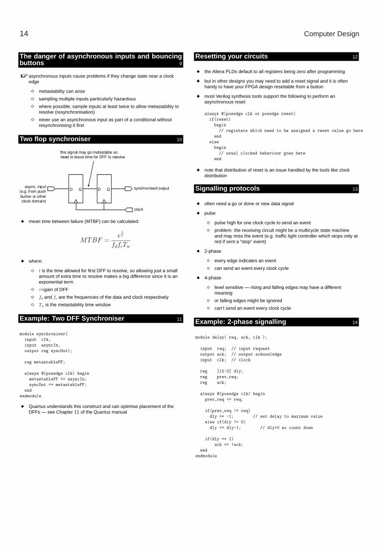
The danger of asynchronous inputs and bouncingbuttons y 9
asynchronous inputs cause problems if they change state near a clockedge
metastability can arise
sampling multiple inputs particularly hazardous
where possible, sample inputs at least twice to allow metastability toresolve (resynchronisation)
never use an asynchronous input as part of a conditional withoutresynchronising it first
Two flop synchroniser y 10
mean time between failure (MTBF) can be calculated:
MTBF =
et
τ
fdfcTw
where:
t is the time allowed for first DFF to resolve, so allowing just a smallamount of extra time to resolve makes a big difference since it is anexponential term
τ=gain of DFF
fd and fc are the frequencies of the data and clock respectively
Tw is the metastability time window
Example: Two DFF Synchroniser y 11
module synchroniser(
input clk,
input asyncIn,
output reg syncOut);
reg metastableFF;
always @(posedge clk) begin
metastableFF <= asyncIn;
syncOut <= metastableFF;
end
endmodule
Quartus understands this construct and can optimise placement of theDFFs — see Chapter 11 of the Quartus manual
Resetting your circuits y 12
the Altera PLDs default to all registers being zero after programming
but in other designs you may need to add a reset signal and it is oftenhandy to have your FPGA design resettable from a button
most Verilog synthesis tools support the following to perform anasynchronous reset:
always @(posedge clk or posedge reset)
if(reset)
begin
// registers which need to be assigned a reset value go here
end
else
begin
// usual clocked behaviour goes here
end
note that distribution of reset is an issue handled by the tools like clockdistribution
Signalling protocols y 13
often need a go or done or new data signal
pulse
pulse high for one clock cycle to send an event
problem: the receiving circuit might be a multicycle state machineand may miss the event (e.g. traffic light controller which stops only atred if sent a “stop” event)
2-phase
every edge indicates an event
can send an event every clock cycle
4-phase
level sensitive — rising and falling edges may have a differentmeaning
or falling edges might be ignored
can’t send an event every clock cycle
Example: 2-phase signalling y 14
module delay( req, ack, clk );
input req; // input request
output ack; // output acknowledge
input clk; // clock
reg [15:0] dly;
reg prev_req;
reg ack;
always @(posedge clk) begin
prev_req <= req;
if(prev_req != req)
dly <= -1; // set delay to maximum value
else if(dly != 0)
dly <= dly-1; // dly>0 so count down
if(dly == 1)
ack <= !ack;
end
endmodule
Lecture 4 — Verilog systems design 15
Example: 4-phase signalling y 15
module loadable_timer(count_from, load_count, busy, clk);
input [15:0] count_from;
input load_count;
output busy;
input clk;
reg busy;
reg [15:0] counter;
always @(posedge clk)
if(counter!=0)
counter <= counter - 1;
else
begin
busy <= load_count; // N.B. wait for both edges of load_count
if(load_count && !busy)
counter <= count_from;
end
endmodule
Combination control paths y 16
typically data-paths have banks of DFFs inserted to pipeline the design
sometimes it can be slow to add DFFs in the control path, especiallyflow-control signals
examples: fifo one A which latches all control signals and fifo one B whichhas a combinational backward flow-control path
design B is faster except when lots of FIFO elements are joined togetherand the combinational path becomes long
Example: FIFO with latched control signals y 17
module f i f o o n e A (/ / c lock & rese tinput c lk ,input r s t ,/ / i npu t s ideinput log ic [ 7 : 0 ] din ,input log ic d i n v a l i d ,output log ic din ready ,/ / ou tput s ideoutput log ic [ 7 : 0 ] dout ,output log ic dou t va l i d ,input log ic dout ready ) ;
log ic f u l l ;always comb begin
f u l l = d o u t v a l i d ;d in ready = ! f u l l ;
end
always f f @( posedge c l k or posedge r s t )i f ( r s t ) begin
d o u t v a l i d <= 1 ’b0 ;dout <= 8 ’ hxx ;
end else i f ( f u l l && dout ready )d o u t v a l i d <= 1 ’b0 ;
else i f ( d in ready & d i n v a l i d ) begindout <= din ;d o u t v a l i d <= 1 ’b1 ;
endendmodule
Example: FIFO with combination reverse controlpath y 18
module f i f o o n e B (/ / c lock & rese tinput c lk ,input r s t ,/ / i npu t s ideinput log ic [ 7 : 0 ] din ,input log ic d i n v a l i d ,output log ic din ready ,/ / ou tput s ideoutput log ic [ 7 : 0 ] dout ,output log ic dou t va l i d ,input log ic dout ready ) ;
log ic f u l l ;always comb begin
f u l l = d o u t v a l i d ;d in ready = ! f u l l | | dout ready ;
end
always f f @( posedge c l k or posedge r s t )i f ( r s t ) begin
d o u t v a l i d <= 1 ’b0 ;dout <= 8 ’ hxx ;
end else i f ( f u l l && dout ready && ! d i n v a l i d )d o u t v a l i d <= 1 ’b0 ;
else i f ( d in ready && d i n v a l i d ) begindout <= din ;d o u t v a l i d <= 1 ’b1 ;
endendmodule
Example: FIFO test bench y 19
module t e s t f i f o o n e A ( ) ;log ic c lk , r s t ;i n i t i a l begin
c l k = 1 ;r s t = 1 ;#15 r s t = 0 ;
endalways #5 c l k = ! c l k ;
log ic [ 7 : 0 ] din , dmiddle , dout ;log ic d i n v a l i d , d in ready ;log ic dmidd le va l id , dmiddle ready ;log ic dou t va l i d , dout ready ;f i f o o n e A stage0 ( . c lk , . r s t , . din , . d i n v a l i d , . d in ready ,
. dout ( dmiddle ) , . d o u t v a l i d ( dm idd le va l i d ) ,
. dout ready ( dmiddle ready ) ) ;f i f o o n e A stage1 ( . c lk , . r s t ,
. d in ( dmiddle ) , . d i n v a l i d ( dm idd le va l i d ) ,
. d in ready ( dmiddle ready ) ,
. dout , . dou t va l i d , . dout ready ) ;
log ic [ 7 : 0 ] s t a t e ;always f f @( posedge c l k or posedge r s t )
i f ( r s t ) begins ta te <= 8 ’d0 ;d i n v a l i d <= 1 ’b0 ;dout ready <= 1 ’b1 ;
end else begini f ( d o u t v a l i d && dout ready )
$display ( ”%05t : f i f o output = %1d ” , $time , dout ) ;i f ( d in ready ) begin
din <= ( s ta te +1)∗3;d i n v a l i d <= 1 ’b1 ;s t a te <= s ta te +1;i f ( s ta te >8) $stop ;
end elsed i n v a l i d <= 1 ’b0 ;
end / / e lse : ! i f ( r s t )endmodule
16 Computer Design
Example: one hot state encoding y 20
states can just have an integer encoding (see last lecture)
but this can result in quite complex if expressions, e.g.:
if(current_state==‘red)
//...stuff to do when in state ‘red
if(current_state==‘amber)
//...stuff to do when in state ‘amber
an alternative is to use one register per state vis:
reg [3:0] four_states;
wire red = four_states[0] || four_states[1];
wire amber = four_states[1] || four_states[3];
wire green = four_states[2];
always @(posedge clk or posedge reset)
if(reset)
four_states <= 4’b0001;
else
four_states <= {four_states[2:0],four_states[3]}; // rotate bits
SystemVerilog pitfalls 1: passing buses around y 21
automatic bus resizing
buses of wrong width get truncated or padded with 0’s
wire [14:0] addr; // oops got width wrong, but no error generated
wire [15:0] data;
CPU the_cpu(addr,data,rw,ce,clk);
MEM the_memory(addr,data,rw,ce,clk);
wires that get defined by default
if you don’t declare a wire in a module instance then it will be a singlebit wire, e.g.:
wire [15:0] addr;
// oops, no data bus declared so just 1 bit wide
CPU the_cpu(addr,data,rw,ce,clk);
MEM the_memory(addr,data,rw,ce,clk);
you pass too few parameters to a module but no error occurs!
SystemVerilog pitfalls 2: naming and parameter or-dering y 22
modules have a flat name space
can be difficult to combine modules from different projects becausethey may share some identical module names with different functions
parameter ordering is easy to get wrong
but you can specify parameter mapping vis:
loadable_timer lt1(.clk(clk), .count_from(timerval),
.load_count(start), .busy(busy));
which is identical to:
loadable_timer lt2(timerval, start, busy, clk);
provided nobody has changed loadable_counter since you lastlooked!
in SystemVerilog there is a short hand for variables passing with identicalnames, e.g. .clk(clk) = .clk
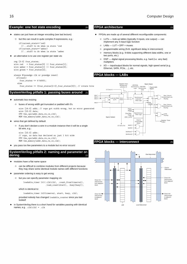
FPGA architecture y 23
FPGAs are made up of several different reconfigurable components:
LUTs — look-up tables (typically 4 inputs, one output) — canimplement any 4-input logic function
LABs — LUT + DFF + muxes
programmable wiring (N.B. significant delay in interconnect)
memory blocks (e.g. 9-kbits supporting different data widths, one ortwo ports, etc.)
DSP — digital signal processing blocks, e.g. hard (i.e. very fast)multipliers
I/O — input/output blocks for normal signals, high speed serial (e.g.Ethernet, SATA, PCIe, ...), etc.
FPGA blocks — LABs y 24
Row, Column,
And Direct Link
Routing
data 1
data 2
data 3
data 4
labclr1
labclr2
Chip-Wide
Reset
(DEV_CLRn)
labclk1
labclk2
labclkena1
labclkena2
LE Carry-In
LAB-Wide
Synchronous
Load
LAB-Wide
Synchronous
Clear
Row, Column,
And Direct Link
Routing
Local
Routing
Register Chain
Output
Register Bypass
Programmable
Register
Register Chain
Routing from
previous LE
LE Carry-Out
Register Feedback
Synchronous
Load and
Clear Logic
Carry
ChainLook-Up Table
(LUT)
Asynchronous
Clear Logic
Clock &
Clock Enable
Select
D Q
ENACLRN
FPGA blocks — interconnect y 25
Direct link
interconnect
from adjacent
block
Direct link
interconnect
to adjacent
block
�������������
A�BCD�
����������
E�FB ����������E��
Direct link
interconnect
from adjacent
block
Direct link
interconnect
to adjacent
block

Lecture 4 — Verilog systems design 17
FPGA blocks — multipliers y 26
CLRN
D Q
ENA
Data A
Data B
aclr
clock
ena
signa
signb
CLRN
D Q
ENA
CLRN
D Q
ENAData Out
Embedded Multiplier Block
������������ABC���
������A
FPGA blocks — simplified single-port memory y 27
CLRN
D Q
ENA
D Q
EN
Data Out
������������A
�����������
AB
memory blocks called “Block RAM” — BRAM
dual-port mode supported, etc. + different data/address widths
Inferring memory blocks y 28
SystemVerilog sometimes has to be written in a particular style in orderthat the synthesis tool can easily identify BRAM
e.g. on Thacker’s Tiny Computer used in the labs, the register file isdefined as:
Word r f b l o c k [0:(1<< $ b i t s ( RegAddr ) ) −1 ] ;RegAddr RFA read addr , RFB read addr ;always f f @( posedge c s i c l k c l k )
begin / / r e g i s t e r f i l e po r t Ai f ( d i v )
r f b l o c k [ IM pos . rw ] <= WD;else
RFA read addr <= IM . payload . ra ;end
assign RFAout = r f b l o c k [ RFA read addr ] ;
always f f @( posedge c s i c l k c l k )RFB read addr <= IM . payload . rb ;
assign RFBout = r f b l o c k [ RFB read addr ] ;
Static timing analysis y 29
place & route — lays out logic onto FPGA
static timing analysis determines timing closure, i.e. that we’ve met timing
TimeQuest does this in Quartus
looks at all paths from outputs of DFFs to inputs of DFFs
max clock period = the worst case delay + DFF hold time + clock jittermargin
Fmax determined — critical that the circuit is clocked at a frequencybelow its Fmax
much effort is made by Altera to ensure static timing analysis isaccurate
Final words on ECAD y 30
Programmable hardware is here to stay, and it likely to become even morewidespread in products (i.e. not just for prototyping)
SystemVerilog is an improvement over Verilog, but a long way to go
active research being undertaken into higher level HDLs
e.g. more recent languages like Bluespec add channelcommunication mechanisms
Hope you enjoy the Lab’s and learning about hardware/software codesign

18 Computer Design

Lecture 5 — Histroical Computer Architecture 19
Computer Design — Lecture 5
Historical Computer Architecture y 1
Overview of this lectureReview early computer design since they provide a good background and arerelatively simple.
What is a “Computer”? y 2
In the “iron age” y 3
Early calculating machines were driven by human operators (this one’s aMarchant).
Form factor? y 4
Analogue Computers y 5
input variables are continuous and vary with respect to time
output respond almost simultaneously to changes in input
support continuous mathematical operators
e.g. additions, subtraction, multiplication, division, integration, etc.
BUT unable to store an manipulate large quantities of data, unlike digitalcomputers
electrical noise affects precision
programs are hardwired
Hardwired Programming Digital Computers y 6
Programs (lists of orders/instructions) were hardwired into the machine.
ColossusStarted/completed: 1943/1943
Project leader: Dr Tommy FlowersProgrammed: pluggable logic & paper tape
Speed: 5000 operations per secondPower consumption: 4.5 KW
Footprint: 360 feet2 (approx) + room for cooling, operatorsNotes: broke German codes, info. vital to success of D-day in
1944
ENIACStarted/completed: 1943/1945
Project leaders: John Mauchly and J. Presper Eckert.Programmed: plug board & switches
Speed: 5000 operations per secondFootprint: 1000 feet2
Birth of the Stored Program Computer y 7
In 1945 John von Neumann wrote “First Draft of a Report on the EDVAC”in which the architecture of the stored-program computer was outlined.
Electronic storage of programming information and data would eliminatethe need for the more clumsy methods of programming, such as punchedpaper tape.
This is the basis for the now ubiquitous control-flow model.
Control-flow model is often called the von Neumann architecture
However, it is apparent that Eckert and Mauchly also deserve a greatdeal of credit.
The Control-flow Model y 8
The processor executes a list of instructions (order codes) using a programcounter (PC) as a pointer into the list, e.g. to execute a=b+c:
20 Computer Design
What is a Processor? y 9
the processor is the primary means of processing information within acomputer
the “engine” of the computer if you like
the processor is controlled by a program
often a list of simple orders or instructions
instructions (and other hardware mechanisms...) form the atomicbuilding blocks from which programs are constructed
executing many millions of instructions per second makes thecomputer look “clever”
A Quick Note on Programming y 10
programs are presented to the processor as machine code
programs written in high level languages have to be compiled intomachine code
Summer School of 1946 y 11
the summer school on Computing at the University of Pennsylvania’sMoore School of Electrical Engineering stimulated post-war constructionof stored-program computers
prompted work on EDSAC (Cambridge), EDVAC and ENIAC (USA)
Manchester team had visited the Moore School but did not attend thesummer school.
Manchester Mark I(The Baby) y 12
Demonstrated: June 1948Project leaders: Tom Kilburn and F C (Freddie) Williams
Input/Output: buttons + memory is visible on Williams tubeMemory: William Tube
32 × 32 bit wordsLogic Technology: valves (vacuum tubes)
Add time: 1.8 msFootprint: medium room
just 7 instructions to subtract, store and conditional jump (see next lecture)
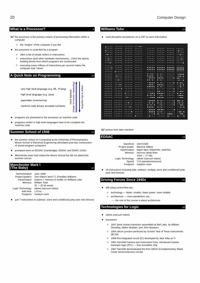
Williams Tube y 13
used phosphor persistence on a CRT to store information
picture from later machine
EDSACy 14
Start/End: 1947/1949Project leader: Maurice Wilkes
Input/Output: paper tape, teleprinter, switchesMemory: mercury delay lines
1024 × 17 bitsLogic Technology: valves (vacuum tubes)
Speed: 714 operations/secondFootprint: medium room
18 instructions including add, subtract, multiply, store and conditional jump(see next lecture)
Driving Forces Since 1940s y 15
still using control-flow but...
technology — faster, smaller, lower power, more reliable
architecture — more parallelism, etc.
— the rest of the course is about architecture
Technologies for Logic y 16
valves (vacuum tubes)
transistors
1947 point contact transistor assembled at Bell Labs. by WilliamShockley, Walter Brattain, and John Bardeen
1954 silicon junction perfected by Gordon Teal of Texas Instruments($2.50)
1958 first integrated circuit (IC) developed by Jack Kilby at TI
1961 Fairchild Camera and Instrument Corp. introduced resistortransistor logic (RTL) — first monolithic chip
1967 Fairchild demonstrated the first CMOS (Complementary MetalOxide Semiconductor) circuits

Lecture 5 — Histroical Computer Architecture 21
Early Intel Processors y 17
Intel 4004 MicroprocessorDemonstrated: 1971
Project team: Federico Faggin, Ted Hoff, et al.Logic Technology: MOS
Data width: 4 bitsSpeed: 60k operations/second
Intel 8008 MicroprocessorDemonstrated: 1972
Logic Technology: MOSData width: 8 bits
Speed: 0.64 MIPS
Xerox PARC y 18
PARC = Palo Alto Research Center
Alto (1974)
chief designer: Chuck Thacker (was in Cambridge working forMicrosoft until recently)
first personal computer (built in any volume) to use a bit-mappedgraphics and mouse to provide a windowed user interface
Ethernet (proposed 1973)
Bob Metcalf (was here for a sabatical) and Dave Boggs
Laser printers...
Xerox failed to capture computer markets — read “Fumbling the Future:how Xerox invented, then ignored, the first personal computer”, D Smithand R Alexander, New York, 1988
Technologies for Primary Memory y 19
mercury delay lines
William’s tube
magnetic drum
core memory
solid state memories (DRAM, SRAM)
Technologies for Secondary Memory y 20
punched paper tape and cards
magnetic drums, disks, tape
optical (CD, etc)
Flash memory
Computing Markets y 21
Servers
availablility (fault tolerance)
throughput is very important (databases, etc)
power (and heat output) is becoming more important
Desktop Computing
market driven by price and performance
benchmarks are office/media/web applications
Embedded Computing
power efficiency is very important
real-time performance requirements
huge growth in 90’s and early 21st centry (mobile phones,automotive, PDAs, set top boxes)
Resources y 22
Colossus:http://www.cranfield.ac.uk/ccc/bpark/colossus
Boston Computer Museum time line:http://www.tcm.org/history/timeline/
Virtual Museum of Computing:http://www.comlab.ox.ac.uk/archive/other/museums/computing.html
Free Online Dictionary of Computing:http://wombat.doc.ic.ac.uk/foldoc/

22 Computer Design
Lecture 6 — Early instruction set architecture 23
Computer Design — Lecture 6
Historical Instruction Set Architecture y 1
Review of Last LectureThe last lecture covered a little history.
Overview of this LectureThis lecture introduces the programmer’s model of two early computers: theManchester Mark I (the baby), and the EDSAC, Cambridge.
Manchester Mark I (The Baby) y 2
Not to be confused with the Farantti Mark 1 which came later.
vital statistics:
32 × 32 bits memory (William’s tube)
two registers: CR = program counter, ACC=accumulator
no real I/O
7 instructions
Manchester Mark I — Instruction Encoding y 3
Manchester Mark I — Instruction Set y 4
function code name description000 JMP sets CR to the contents of LINE100 JRP adds the contents of LINE to CR010 LDN gets the contents of LINE, negated, into ACC110 STO stores the contents of ACC into LINE001 or 101 SUB subtracts the contents of LINE from ACC,
putting the result in ACC011 TEST if the contents of ACC are less than zero,
add 1 to CR (skip next instruction)111 STOP halt the machine
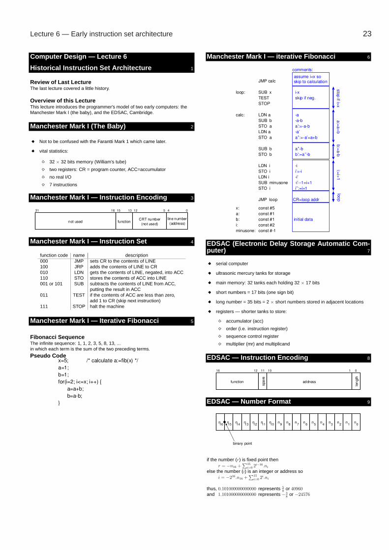
Manchester Mark I — Iterative Fibonacci y 5
Fibonacci SequenceThe infinite sequence: 1, 1, 2, 3, 5, 8, 13, ...in which each term is the sum of the two preceding terms.
Pseudo Code
Manchester Mark I — iterative Fibonacci y 6
EDSAC (Electronic Delay Storage Automatic Com-puter) y 7
serial computer
ultrasonic mercury tanks for storage
main memory: 32 tanks each holding 32 × 17 bits
short numbers = 17 bits (one sign bit)
long number = 35 bits = 2 × short numbers stored in adjacent locations
registers — shorter tanks to store:
accumulator (acc)
order (i.e. instruction register)
sequence control register
multiplier (mr) and multiplicand
EDSAC — Instruction Encoding y 8
EDSAC — Number Format y 9
if the number (r) is fixed point thenr = −n16 +
∑15
i=02i−16.ni
else the number (i) is an integer or address soi = −216.n16 +
∑15
i=02i.ni
thus, 0.101000000000000 represents 5
8or 40960
and 1.101000000000000 represents −3
8or −24576

24 Computer Design
EDSAC — Instruction Format y 10
Instruction DescriptionP n pseudo code (for constants) instruction is nA n add acc:=acc+(n)S n subtract acc:=acc-(n)H n init. multiplier mr:=(n)V n multiply and add acc:=acc+mr×(n)N n multiply and subtract acc:=acc-mr×(n)T n store and clear acc (n):=acc, acc:=0U n store (n):=accC n bitwise AND acc:=mr AND (n) + accR 2n−2 shift right acc:=acc×2−n
L 2n−2 shift left acc:=acc×2n
E n conditional branch acc>= 0 if(acc>=0) pc:=nG n conditional branch acc< 0 if(acc<0) pc:=nI n input 5 bit from punched tape (n):=punch tape inputO n output top 5 bits to teleprinter output:=(n)F n read character next output char. (n):=outputX round accumulator to 16 bitsY round accumulator to 34 bitsZ stop the machine and ring warning bell
Each instruction is postfixed with S or L to indicate whether it refers to Shortwords or Long words (S = 0, L = 1).
EDSAC — Iterative Fibonacci y 11
Problems with Early Machines y 12
technology limited memory size, speed, reliability, etc.
instruction set does not support:
subroutine calls
floating point operations
minimal support for bit wise logic operations (AND, OR, etc)
functions not invented then, nor:
interrupts, exceptions, memory management, etc. (see futurelectures)
instructions have only one operand
so each instruction does little work
Stack Machines y 13
operand stack replaces accumulator
allows more intermediate results to be stored within the processor
reduces load on memory bus (von Neumann bottleneck)
equations easily manipulated into reverse Polish notation
some stack machines supported a data stack for parameter passing,storing return addresses and local variables (see Compilers course)
Stack Program Example — Fibonacci y 14
Register Machines y 15
register file = small local memory used to store intermediate results
physically embedded in the processor for fast access
it is practical for small memories to be multiported (i.e. many simultaniousreads and writes)
allows for parallelism (more later...)
Number of Operands Per Instruction y 16
EDSAC and Baby instructions
— single operand per instruction (address)
— accumulator implicit in most instructions
stack machines also usually just have one operand
register machines can have multiple operands, e.g.:
add r1,r2,r3
— adds contents of registers r2 and r3 and writes the result in r1
— memory bus not even used to complete this!
load r4,(r5+#8)
— calculates an address by adding the constant 8 to the contents ofregister r5, loads a value from this calculated address and storesthe result in r4
these instructions are independent of each other, so could execute inparallel (more later...)

Lecture 7 — Thacker’s Tiny Computer 3 25
Computer Design — Lecture 7
Thacker’s Tiny Computer 3 y 1
Overview of this lectureReview Thacker’s Tiny Computer 3 used in the ECAD+Arch labs.
The paper is attached to the handout.
Instruction format y 2
��������������
� �ABC �D EF�� ����� ���� ������
EF�������
������ !
������"!
�����! �
�����!"�
�������#�!
�������$�!
��%����&�!
�����'�(�')��
������*'��A��(�'�+��,�
��������(����
������C-��
������C-�.
������C-�%
�����
�������)�'
������B/0�
������B/1�
�����2���3
�������
�������'4A5���1E*�A6ED,6�(����������������
�����(��'�78��789�D:1�A6��1E*�A6�D,6�(����������������
�����(��'�28��289�D:1�A6��1E*�A6�D,6�(����������������
������F����F���'�D�6��1E*�A6�D,6�(����������������
�����5�A�78���1789�D:6��B/1E*�A6�D,6�(����������������
����������1��;�A�A6��B/1E*�A6�D,6�(����������������
��%��<F4����1=C �6�=C1E*�A6�D,6����(���
�����'�(�')��
BC15�A�����(�A���*D��(���������������(�'F�����,6����(���
=C1�'�+'A4���F���'
�B/1EF������*�A6�D,6���'������EF��������(�(����>���D3�����EF���D��(
E*�A6�D,1'��A��*�����6��B/,6���'������'��A������(�(����>���D3�����������D��(
Chuck Thacker’s schematic y 3
���������
�A B C
DE
F���
��
���C����
��� F���
� F���
���C����
������
��� � �C�����
!�
� � ��"��#
�$ B C
������%����
��"��#
�$ B C
DE"�&
�' DE��%
��
D(�
���C��)�
���C��*�
����+����
��
�F���
F%,�
-%,�
F ���
- ���
� ���
-���
���� .���
F/0�C�����
D(�
D(�
F��' ��1' /���%
���2�C�
�%,�D(�
D(�
D(� �%,�
�%,�
!
DE��%
DE
E'3
E'3 ����#
�' ���C����
4�"�
/� �E����
��
/� �
�������,�%�
������
4�"� DE��,
���5�*�
���+�)�E#%,�
D(�
D(� �%,�
�%,�
Example program y 4
machine code (instruction fields) assembler codeRw LC Ra Rb Func Shift Skip Opcode label assember commentr1 0 r1 r1 AND - - IN r1 <- in # get input parameterr2 1 1 lc r2 1 # a=1r3 1 1 lc r3 1 # b=1r4 1 7 lc r4 test # r4=addr. of testr4 0 r4 r4 AND - - JMP jmp r4 # jump testr2 0 r2 r3 ADD - - - loop: r2 r2 r3 add # a=a+br3 0 r2 r3 SUB - - - r2 r2 r3 sub # b=a-br4 1 5 test: lc r4 loop # r4=addr. of loopr1 0 r1 r1 DEC - LEZ - dec r1 ?<0 # r1−−; if(r1<=0) skipr4 0 r4 r4 AND - - jmp r4 # jump loopr3 0 r3 r3 AND - - OUT r3 ->out # output result in r3r21 1 12 lc r21 end # r21=addr. of endr21 0 r21 r21 AND - - JMP end: jmp r0 r21 # jump end, return address in r0
Simulation trace for fib(3) y 5
# 20: Test data being sent# 50: PC=0x00 rw=r01= 3=0x00000003 ra=r01=0xxxxxxxxx rb=r01=0xxxxxxxxx func=AND r o t a t e =NSH sk ip=NSK op=IN# 60: Test data being sent# 70: PC=0x02 l c rw=r02=1# 90: PC=0x03 l c rw=r03=0# 110: PC=0x04 l c rw=r04=7# 130: PC=0x04 rw=r04= 5=0x00000005 ra=r04=0x00000007 rb=r04=0x00000007 func=AND r o t a t e =NSH sk ip=NSK op=JMP# −−−−−−−−−−−−−−−−−−−−−−−−−−−−−−−−−−−−−−−−# 150: PC=0x08 l c rw=r04=5# 170: PC=0x08 rw=r01= 2=0x00000002 ra=r01=0x00000003 rb=r01=0x00000003 func=DEC r o t a t e =NSH sk ip=LEZ op=FUN# 190: PC=0x09 rw=r04= 10=0x0000000a ra=r04=0x00000005 rb=r04=0x00000005 func=AND r o t a t e =NSH sk ip=NSK op=JMP# −−−−−−−−−−−−−−−−−−−−−−−−−−−−−−−−−−−−−−−−# 210: PC=0x05 rw=r02= 1=0x00000001 ra=r02=0x00000001 rb=r03=0x00000000 func=ADD r o t a t e =NSH sk ip=NSK op=FUN# 230: PC=0x06 rw=r03= 1=0x00000001 ra=r02=0x00000001 rb=r03=0x00000000 func=SUB r o t a t e =NSH sk ip=NSK op=FUN# 250: PC=0x08 l c rw=r04=5# 270: PC=0x08 rw=r01= 1=0x00000001 ra=r01=0x00000002 rb=r01=0x00000002 func=DEC r o t a t e =NSH sk ip=LEZ op=FUN# 290: PC=0x09 rw=r04= 10=0x0000000a ra=r04=0x00000005 rb=r04=0x00000005 func=AND r o t a t e =NSH sk ip=NSK op=JMP# −−−−−−−−−−−−−−−−−−−−−−−−−−−−−−−−−−−−−−−−# 310: PC=0x05 rw=r02= 2=0x00000002 ra=r02=0x00000001 rb=r03=0x00000001 func=ADD r o t a t e =NSH sk ip=NSK op=FUN# 330: PC=0x06 rw=r03= 1=0x00000001 ra=r02=0x00000002 rb=r03=0x00000001 func=SUB r o t a t e =NSH sk ip=NSK op=FUN# 350: PC=0x08 l c rw=r04=5# 370: PC=0x08 rw=r01= 0=0x00000000 ra=r01=0x00000001 rb=r01=0x00000001 func=DEC r o t a t e =NSH sk ip=LEZ op=FUN# 390: PC=0x09 rw=r04= 10=0x0000000a ra=r04=0x00000005 rb=r04=0x00000005 func=AND r o t a t e =NSH sk ip=NSK op=JMP# −−−−−−−−−−−−−−−−−−−−−−−−−−−−−−−−−−−−−−−−# 410: PC=0x05 rw=r02= 3=0x00000003 ra=r02=0x00000002 rb=r03=0x00000001 func=ADD r o t a t e =NSH sk ip=NSK op=FUN# 430: PC=0x06 rw=r03= 2=0x00000002 ra=r02=0x00000003 rb=r03=0x00000001 func=SUB r o t a t e =NSH sk ip=NSK op=FUN# 450: PC=0x08 l c rw=r04=5# 470: PC=0x08 rw=r01= 4294967295=0 x f f f f f f f f ra=r01=0x00000000 rb=r01=0x00000000 func=DEC r o t a t e =NSH sk ip=LEZ op=FUN# 490: PC=0x0a rw=r03= 2=0x00000002 ra=r03=0x00000002 rb=r03=0x00000002 func=AND r o t a t e =NSH sk ip=NSK op=OUT# 500: >>>>>>>>>> output = 0x00000002 = 2 <<<<<<<<<<
# 510: PC=0x0c l c rw=r21=12# 530: PC=0x0c rw=r00= 13=0x0000000d ra=r21=0x0000000c rb=r21=0x0000000c func=AND r o t a t e =NSH sk ip=NSK op=JMP# −−−−−−−−−−−−−−−−−−−−−−−−−−−−−−−−−−−−−−−−# STOP c o n d i t i o n i d e n t i f i e d − l oop ing on the spot# Break i n Module DisplayTraces a t t t c . sv l i n e 113# Simula t ion Breakpoint : Break i n Module DisplayTraces a t t t c . sv l i n e 113# MACRO . / t t c s i m f i b . do PAUSED at l i n e 20
Structural vs. Behavioural implementation style y 6
For our SystemVerilog version of the TTC we’ve used a more behaviouralstyle
A good example of this is the ALU where we describe what functions werequire and Thacker describes the logic on a per bit basis
The structrual approach makes it clear how many logic blocks are likely tobe used
The behavioural approach allows the synthesis tools to use other FPGAresources like DSP blocks
Timing of SystemVerilog version y 7
Thacker’s TTC using two clocks breaking operations down into phases
We used one clock and only the positive edge of it
Our design breaks execution into two steps:
1. instruction fetch followed by decode
2. register fetch, ALU operation, shift, write-back, memory access,branch
The critical path is through register fetch → ALU → shift → write-back
The design is not pipelined unlike modern machines (see later lectures)
ttc.sv — types y 8
/∗ ∗∗∗∗∗∗∗∗∗∗∗∗∗∗∗∗∗∗∗∗∗∗∗∗∗∗∗∗∗∗∗∗∗∗∗∗∗∗∗∗∗∗∗∗∗∗∗∗∗∗∗∗∗∗∗∗∗∗∗∗∗∗∗∗∗∗∗∗∗∗∗∗∗∗∗∗∗ Thacker ’ s Tiny Computer 3 i n SystemVeri log∗ ==========================================∗ Copyr ight Simon Moore and Frankie Robertson , 2011∗∗∗∗∗∗∗∗∗∗∗∗∗∗∗∗∗∗∗∗∗∗∗∗∗∗∗∗∗∗∗∗∗∗∗∗∗∗∗∗∗∗∗∗∗∗∗∗∗∗∗∗∗∗∗∗∗∗∗∗∗∗∗∗∗∗∗∗∗∗∗∗∗∗∗∗ ∗ /
typedef log ic [ 6 : 0 ] RegAddr ;typedef log ic [ 9 : 0 ] ProgAddr ;typedef log ic [ 9 : 0 ] DataAddr ;typedef log ic [ 3 1 : 0 ] Word ;typedef log ic signed [ 3 1 : 0 ] SignedWord ;
/ / enumeration types desc r ib ing f i e l d s i n the i n s t r u c t i o ntypedef enum logic [ 2 : 0 ] {ADD,SUB, INC ,DEC,AND,OR,XOR} Func ;typedef enum logic [ 1 : 0 ] {NSH,RCY1,RCY8,RCY16} Rotate ;typedef enum logic [ 1 : 0 ] {NSK, LEZ ,EQZ, INR} Skip ;typedef enum logic [ 2 : 0 ] {FUN,STD, STI ,OUT,LDD, IN ,JMP} Op;
/ / s t r u c t u r e desc r ib ing the i n s t r u c t i o n formattypedef s t ruc t packed {
RegAddr rw ;log ic l c ;s t ruc t packed {
RegAddr ra ;RegAddr rb ;Func func ;Rotate r o t a t e ;Skip sk ip ;Op op ;
} payload ;} I n s t ;
26 Computer Design
ttc.sv — helper functions y 9
/ / f u n c t i o n to determine i f a sk ip i s to be performedfunct ion log ic s k i p t e s t e r ( I n s t i n s t r u c t i o n , SignedWord a l u r e s u l t ) ;
r e t u r n ! i n s t r u c t i o n . l c && ( ( ( i n s t r u c t i o n . payload . sk ip == LEZ) && ( a l u r e s u l t < 0 ) ) | |( ( i n s t r u c t i o n . payload . sk ip == EQZ) && ( a l u r e s u l t == 0 ) ) ) ;
endfunction
/ / f u n c t i o n to determine the next program counter valuefunct ion ProgAddr pc mux ( log ic jump , log ic skip , log ic reset mode ,
SignedWord a l u r e s u l t , Word pc ) ;i f ( reset mode ) r e t u r n 0 ;else i f ( jump ) r e t u r n a l u r e s u l t [ 9 : 0 ] ;else i f ( sk ip ) r e t u r n pc + 2;else r e t u r n pc + 1;
endfunction
/ / f u n c t i o n to decode the opcodefunct ion log ic [ 6 : 0 ] opcode decode ( I n s t i n s t r u c t i o n ) ;
r e t u r n ( i n s t r u c t i o n . l c ? 0 : 7 ’ h7f )& { i n s t r u c t i o n . payload . op == STD,
i n s t r u c t i o n . payload . op == STI ,i n s t r u c t i o n . payload . op == OUT,i n s t r u c t i o n . payload . op == LDD,i n s t r u c t i o n . payload . op == IN ,i n s t r u c t i o n . payload . op == JMP,! i n s t r u c t i o n . payload . op [ 2 ] } ;
endfunction
/ / f u n c t i o n implementing the r e s u l t m u l t i p l e x e rfunct ion Word r e g f i l e w r i t e d a t a m u x ( I n s t i n s t r u c t i o n , log ic jump ,
log ic l oad a lu , log ic load dm , log ic in ,ProgAddr pc , SignedWord alu , Word dm, Word a s i i n d a t a ) ;
i f ( jump ) r e t u r n pc + 1;else i f ( i n s t r u c t i o n . l c ) r e t u r n Word ’ ( i n s t r u c t i o n . payload ) ;else i f ( l oad a lu ) r e t u r n a lu ;else i f ( load dm ) r e t u r n dm;else i f ( i n ) r e t u r n a s i i n d a t a ;else r e t u r n 1 ’ bx ;
endfunction
/ / f u n c t i o n to implement the ALU and s h i f t e rfunct ion SignedWord a lu ( I n s t i n s t r u c t i o n , Word r f a o u t , Word r f b o u t ) ;
SignedWord p r e s h i f t ;unique case ( i n s t r u c t i o n . payload . func )
ADD: p r e s h i f t = r f a o u t + r f b o u t ;SUB: p r e s h i f t = r f a o u t − r f b o u t ;INC : p r e s h i f t = r f b o u t + 1 ;DEC: p r e s h i f t = r f b o u t − 1;AND: p r e s h i f t = r f a o u t & r f b o u t ;OR: p r e s h i f t = r f a o u t | r f b o u t ;XOR: p r e s h i f t = r f a o u t ˆ r f b o u t ;
defau l t : p r e s h i f t = 1 ’ bx ;endcase ;case ( i n s t r u c t i o n . payload . r o t a t e )
NSH: r e t u r n p r e s h i f t ;RCY1: r e t u r n { p r e s h i f t , p r e s h i f t } >> 1;RCY8: r e t u r n { p r e s h i f t , p r e s h i f t } >> 8;RCY16: r e t u r n { p r e s h i f t , p r e s h i f t } >> 16;
endcase ;endfunction
ttc.sv — module to help with debug y 10
/ / he lper module f o r debug purposesmodule DisplayTraces (
input c lk , input enable , input i n t t r a c e l e v e l ,input I n s t i , input Jump , input ProgAddr PC,input Word WD, input Word RFAout , input Word RFBout ) ;
ProgAddr oldPC =0;always @( posedge c l k )
i f ( enable )i f ( t r a c e l e v e l ==1)
begin$wr i t e ( ”%05t : ” , $t ime ) ; / / ou tput s imu la t i on t imei f ( i . l c ) / / d i sp l ay load−constant i n s t r u c t i o n s
$display ( ”PC=0x%02x l c rw= r%02d=%1d ” ,PC, i . rw ,WD) ;else / / d i sp l ay o ther i n s t r u c t i o n s
begin$wr i t e ( ”PC=0x%02x rw= r%02d=%11d=0x%08x ra= r%02d=0x%08x rb= r%02d=0x%08x ” ,
oldPC , i . rw ,WD,WD, i . payload . ra , RFAout , i . payload . rb , RFBout ) ;$display ( ” func=%s r o t a t e=%s sk ip=%s op=%s ” ,
i . payload . func , i . payload . ro ta te , i . payload . skip , i . payload . op ) ;end
i f (Jump) $display ( ”−−−−−−−−−−−−−−−−−−−−−−−−−−−−−−−−−−−−−−−−” ) ;i f (PC==oldPC )
begin$display ( ”STOP c o n d i t i o n i d e n t i f i e d − l oop ing on the spot ” ) ;$stop ;
endoldPC <= PC;
end / / i f ( debug trace ==1)else
begini f ( i . payload . op==IN )
$display ( ”%05t : i npu t =0x%08x ” , $time ,WD) ;i f ( i . payload . op==OUT)
$display ( ”%05t : ou tput=0x%08x ” , $time , RFAout ) ;end / / e lse : ! i f ( t r a c e l e v e l ==1)
endmodule
ttc.sv — Test bench y 11
module TestTinyComp ( ) ;/ / parameters f o r the i n s t r u c t i o n ROM i n i t i a l i s a t i o nparameter progpath mi f= ” ” ;parameter progpath rmb= ” ” ;/ / parameter to determine the debug l e v e lparameter debug trace =1;
log ic c s i c l k c l k , r s i r e s e t r e s e t ;log ic o u t v a l i d ;Word out da ta ;log ic i n v a l i d , i n ready ;Word i n d a t a ;log ic [ 7 : 0 ] i n s t a t e ;log ic i n s t r u c t i o n c o m p l e t e ;
TinyComp #(. p rogpath mi f ( p rogpath mi f ) ,. progpath rmb ( progpath rmb ) ,. debug trace ( debug trace )) dut (
/ / pass parameters w i th matching names.∗ ,
/ / n u l l data memory i n t e r f a c e. avm m1 address ( ) ,. avm m1 read ( ) ,. avm m1 readdata ( ) ,. avm m1 write ( ) ,. avm m1 writedata ( ) ,. avm m1 waitrequest (1 ’ b0 ) ,
/ / ou tput stream. aso out data ( ou t da ta ) ,. a s o o u t v a l i d ( o u t v a l i d ) ,. aso out ready (1 ’ b1 ) ,
/ / i npu t stream. a s i i n d a t a ( i n d a t a ) ,. a s i i n v a l i d ( i n v a l i d ) ,. a s i i n r e a d y ( in ready )) ;
/ / i n i t i a l i s e c lock and rese ti n i t i a l begin
c s i c l k c l k = 1 ;r s i r e s e t r e s e t = 1 ;#20
r s i r e s e t r e s e t = 0 ;end
/ / o s c i l a t e the c lockalways #5 c s i c l k c l k = ! c s i c l k c l k ;
/ / t e s t sequencer which sends two values on to the TTC on i t s In stream/ / and d isp lays the r e s u l t s from the Out streamalways @( posedge c s i c l k c l k or posedge r s i r e s e t r e s e t )
i f ( r s i r e s e t r e s e t )begin
i n s t a t e <= 0;i n v a l i d <= 0;i n d a t a <= 0;
endelse
begini f ( o u t v a l i d )
$display ( ”%05t : >>>>>>>>>> output = 0x%08x = %1d <<<<<<<<<<” , $time , out data , ou ti f ( i n ready )
i n v a l i d <= 0;else
i f ( ! i n v a l i d ) / / on ly send data once the l a s t l o t has been consumedbegin
case ( i n s t a t e )0 : i n d a t a <= 32 ’d10 ;1 : i n d a t a <= 32 ’d99 ;2 : i n d a t a <= 32 ’d2 ;3 : i n d a t a <= 32 ’d3 ;defau l t : i n d a t a <= 32 ’h0 ;
endcase / / case ( i n s t a t e )i f ( i n s t a t e <4)
begin$display ( ”%05t : Test data being sent ” , $t ime ) ;i n s t a t e <= i n s t a t e +1;i n v a l i d <= 1;
endend
end
endmodule / / TestTinyComp

Lecture 7 — Thacker’s Tiny Computer 3 27
ttc.sv — TinyComp module (part 1) y 12
module TinyComp (/ / c lock and rese t i n t e r f a c einput c s i c l k c l k ,input r s i r e s e t r e s e t ,
/ / avalon master f o r data memory ( unused i n labs )output DataAddr avm m1 address ,output log ic avm m1 read ,input Word avm m1 readdata ,output log ic avm m1 write ,output Word avm m1 writedata ,input log ic avm m1 waitrequest ,
/ / avalon i npu t stream f o r IN i n s t r u c t i o n sinput Word a s i i n d a t a ,input log ic a s i i n v a l i d ,output log ic as i i n ready ,
/ / avalon output stream f o r OUT i n s t r u c t i o n soutput Word aso out data ,output log ic aso ou t va l i d ,input log ic aso out ready ,
/ / exported s i g n a l f o r connect ion to an a c t i v i t y LEDoutput log ic i n s t r u c t i o n c o m p l e t e) ;
/ / parameters f o r the i n s t r u c t i o n ROM i n i t i a l i s a t i o nparameter progpath mi f= ” ” ;parameter progpath rmb= ” ” ;/ / parameter to determine the debug l e v e lparameter debug trace =1;
/ / dec lare v a r i a b l e sSignedWord WD;Word RFAout , RFBout ;ProgAddr PC, PCmux, im addr ;SignedWord ALU;Word DM;I n s t IM , IM pos ;log ic doSkip , WriteIM , WriteDM , Jump , LoadDM, LoadALU , In , Out ;log ic div , phase0 , phase1 ;log ic [ 1 : 0 ] d i v r e s e t d l y ;
/ / i n s t a n t i a t e he lper module to do t r a c i n g i n s imu la t i on‘ i f d e f MODEL TECHDisplayTraces d t ( c s i c l k c l k , phase1 , debug trace , IM pos ,
Jump , PCmux, WD, RFAout , RFBout ) ;‘ end i f
/ / i n s t r u c t i o n memory (ROM) i n i t i a l i s e d f o r Quartus(∗ r a m i n i t f i l e = progpath mi f ∗ ) I n s t im block [0:(1<< $ b i t s ( ProgAddr ) ) −1 ] ;i n i t i a l begin / / i n i t i a l i s a t i o n o f ROM f o r ModelSim
‘ i f d e f MODEL TECH$readmemb ( progpath rmb , im block ) ;‘ end i f
endalways @( posedge c s i c l k c l k )
im addr <= PCmux;assign IM = im block [ im addr ] ;
/ / implement the r e g i s t e r f i l eWord r f b l o c k [0:(1<< $ b i t s ( RegAddr ) ) −1 ] ;RegAddr RFA read addr , RFB read addr ;always f f @( posedge c s i c l k c l k )
begin / / r e g i s t e r f i l e po r t Ai f ( d i v )
r f b l o c k [ IM pos . rw ] <= WD;else
RFA read addr <= IM . payload . ra ;end
assign RFAout = r f b l o c k [ RFA read addr ] ;
always f f @( posedge c s i c l k c l k )RFB read addr <= IM . payload . rb ;
assign RFBout = r f b l o c k [ RFB read addr ] ;
/ / combinat iona l l o g i calways comb
beginphase0 = ! d i v ;phase1 = d iv && ! avm m1 waitrequest &&
( ( ! In && ! Out ) | | ( Out && ! a s o o u t v a l i d ) | | ( In && a s i i n v a l i d ) ) ;DM = avm m1 readdata ;ALU = alu ( IM pos , RFAout , RFBout ) ;doSkip = s k i p t e s t e r ( IM pos , ALU ) ;PCmux = pc mux (Jump , doSkip , d i v r e s e t d l y [ 1 ] , ALU, PC) ;WD = r e g f i l e w r i t e d a t a m u x ( IM pos , Jump , LoadALU , LoadDM, In , PC, ALU, DM, a s i i n d a t a ) ;a s i i n r e a d y = ( In && d iv ) ;avm m1 write = WriteDM && d iv ;avm m1 read = LoadDM && d iv ;avm m1 address = DataAddr ’ ( RFBout ) ;avm m1 writedata = RFAout ;
end
ttc.sv — TinyComp module (part 2) y 13
/ / the main always block implementing the processoralways f f @( posedge c s i c l k c l k ) / / or posedge r s i r e s e t r e s e t )
i f ( r s i r e s e t r e s e t )begin
d iv <= 0;d i v r e s e t d l y <= 3;PC <= 0;{WriteDM , WriteIM , Out , LoadDM, In , Jump , LoadALU} = 7 ’b0 ;a s o o u t v a l i d <= 1 ’b0 ;
endelse
begini f ( aso out ready && a s o o u t v a l i d )
a s o o u t v a l i d <= 1 ’b0 ;i f ( phase0 )
beginIM pos <= IM ;{WriteDM , WriteIM , Out , LoadDM, In , Jump , LoadALU} <= opcode decode ( IM ) ;
endi f ( phase1 )
begind iv <= 1 ’b0 ;PC <= PCmux;i f ( Out )
begina s o o u t v a l i d <= 1 ’b1 ;aso out data <= RFAout ;
endi n s t r u c t i o n c o m p l e t e <= 1 ’b1 ;
endelse
begini n s t r u c t i o n c o m p l e t e <= 1 ’b0 ;d i v <= ! ( | d i v r e s e t d l y ) ;d i v r e s e t d l y <= { d i v r e s e t d l y [ 0 ] , 1 ’ b0 } ;
endend
endmodule

28 Computer Design

lecture 8 — System-on-FPGA Design 29
Computer Design — Lecture 8
Systems-on-FPGA y 1
Overview of this lectureExplore systems-on-FPGA design
Review Altera’s Qsys tool and design motivations
Support Materials y 2
Altera video:http://www.altera.com/education/webcasts/all/
wc-2011-conquer-fpga-complexity.html
Altera white paper (copy at the end of the handout):http://www.altera.com/literature/wp/wp-01149-noc-qsys.pdf
Motivation y 3
facilitate reusuable components through standard interfaces
use parameterisable communication fabric on-chip
much research and industry work on networks-on-chip (NoCs),including in Cambridge
make it easier to connect components together
SystemVerilog is not good at interfaces — interfaces are just wires tothe synthesis tool without higher level semantics (e.g. channels)
a graphical approach can make it easier to rapidly build systems (possiblytrue but debatable...)
Avalon Interconnects y 4
AvalonMM — Avalon Memory Mapped interface
used to connect memory mapped masters and slaves in a switchedinterconnect but with bus-like interfaces at the end points
AvalonST — Avalon STreaming interface
represents point-to-point communcation channels between devices
you’ll use this sort of interface in the labs
AvalonMM Example from Quartus 11 manual y 5
���������
M
��A�BC��DD��
DDR3
Controller
DDR3 Chip
Data
Memory
S
Instruction
M
Data
MM
Control
Read Write
Instruction
Memory
Master Command Connectivity
Slave Response Connectivity
Interface to Off-Chip Device
M
S
Avalon-MM Master Port
Avalon-MM Slave Port
TC Avalon Tri-state Conduit
Flash
Memory
Chip
S
SSS
Ethernet
MAC/PHY
Chip
S
E��F�B�����C�����D�B����
Tristate Conduit
Pin Sharer and Bridge
�BC����BB��C
Qsys Design
in Altera FPGA
�A�
A����B����C�����D�B����
TC TC
���C����C�����BC�� ���
�D�����C�����BC�� ���
AvalonMM signals y 6
Basic signals neede for an AvalonMM master interface with default naming:
outputs:
avm_m1_address — address of device to access
avm_m1_read — bit to indicate if a read is requested
avm_m1_write — bit to indicate if a write is requested
avm_m1_writedata — any data to be written
inputs:
avm_m1_readdata — data returned on read request
avm_m1_waitrequest — bit to indicate if the master should wait
other signals to do byte access, burst transfers, etc.
much more information in the Quartus manual (Chapter 7) with timinginformation shown by Qsys tool when importing interfaces
Avalon Streaming Interfaces (AvalonST) y 7
The most basic streaming interface
Data Source Data Sinkdata
A complete streaming interfaceready
Data Source Data Sink
valid
channel
startof packet
endofpacket
empty
error
data
AvalonST interfaces on the TTC y 8
Input stream:
asi_in_data — input data (32-bits wide)
asi_in_valid — input bit indicating if data is valid
asi_in_ready — bit output from TTC to indicate that it’s ready toreceive more data
Output stream:
aso_out_data — output data (32-bits wide)
aso_out_valid — output bit indicating when data is valid
aso_out_ready — input bit indicating when the consumer is ready toreceive data

30 Computer Design

Lecture 9 — RISC Processor Design 31
Computer Design — Lecture 9
RISC Processor Design y 1
Review of the last lectureLast lecture we talked about early computers.
Overview of this lectureThis lecture is about RISC processor design and the MIPS and ARMinstruction sets.
The Design Space y 2
a complex set of inter-related problems ranging from physical constraintsto market forces
requires spiralling refinement
driven by benchmarks – synthetic applications like SPEC marks
hardware is highly parallel
to attain high performance we must exploit parallelism
data has spatial and temporal characteristics
it takes time and (usually) power to move data from one place toanother
digital electronics is improving at a phenomenal pace (Moore’s law - seelecture 1)
but new challenges for nano CMOS: reliability issues, increaseddevice variability, across chip wires have stopped scaling...
Design Goals y 3
Amdahl’s Law and theQuantitative Approach to Processor Design
speedup =performance for the entire task without using the enhancement
performance for entire task using the enhancement when possible
Amdahl’s version: if an optimisation improves a fraction f of execution time by afactor of a then:
speedup =Told
((1− f) + f/a)Told
=1
(1− f) + f/a
example: if a program spends 80% of its time doing multiplies and wewant it to go 4 times faster, how much faster must the multiply be?
⇒ make the common case fast
forms the basis of quantitative processor design and the ReducedInstruction Set Computer (RISC) philosophy
Some Fallacies y 4
MIPS (Millions of Instructions Per Second) is an accurate measure forcomparing performance among computers
there is such a thing as a typical program
synthetic benchmarks predict performance for real programs
peak performance tracks observed performance
you can design a flawless architecture
Pitfall: Eliminating the Semantic Gap y 5
in the 1970s it was vogue to minimise the semantic gap between high levellanguages and assembler in order to improve on performance
this resulted in the CISC (complex instruction set computer) era fromwhich the Intel x86 series is still trying to escape
but by giving too much semantic content to the instruction the usefulnessof the instruction was either limited or so general and complex that it wasslow
Overview of the MIPS Processor y 6
market — originally (1980s) for workstations, but now used mostely inembedded/low power systems (PDAs, set top boxes, machine control etc)requiring good MIPS/Watt
The ARM processor (local company) is more domenant in theembedded systems space but MIPS is now taught so that a completeprocessor design can be presented without ARM’s lawyers gettingupset
instruction set — RISC — a load/store architecture: only special load andstore instructions can access memory, everything else isregister-to-register
registers — 32 registers, each 32-bit long
An Alternative: The ARM Processor y 7
Similar to MIPS but UK designed by Acorn (who did the BBC Micro)
architects: Steve Furber and Roger Wilson
ARM Ltd was a subsidiary of Acorn
Acorn doesn’t exist but ARM is going strong
most mobile phone have an ARM processor
iPods have 3 ARM processors, iPhone has 5
ARM is (unsually) an intellectual property (IP) licensing company (i.e. theylicense designs but make no chips)
no longer taught because I wanted to produce a cut down FPGAimplementation for this course but they were unhappy about the IPissues, so I switched to MIPS for 2007
Example: Iterative Fibonacci Calculation y 8
# assume x is held in $a0 at startaddi $t1, $zero, 1 # initialisationaddi $t2, $zero, 1addi $t3, $zero, 2
loop: sub $t0, $t3, $a0 # if i > xbgtz $t0, finish # then jump to finishadd $t1, $t1, $t2 # a := a + bsub $t2, $t1, $t2 # b := a - baddi $t3, $t3, 1 # i := i + 1j loop
finish: add $v0, $zero, $t1 # return the result in $v0
where x is held in register $a0a is held in register $t1b is held in register $t2i is held in register $t3
would normally be wrapped up as a subroutine...more later...

32 Computer Design
The MIPS Register File (application’s view) y 9
A register file is used to localise intermediate results which improvesperformance. The MIPS provides:
32 x 32 bit registers
HI and LO registers for the results of mult and div operations (more later)
PC; the program counter
Name Number Use Callee must preserve$zero $0 constant 0 N/A$at $1 assembly temporary no$v0 - $v1 $2 - $3 function returns no$a0 - $a3 $4 - $7 function arguments no$t0 - $t7 $8 - $15 temporaries no$s0 - $s7 $16 - $23 saved temporaries yes$t8 - $t9 $24 - $25 temporaries no$k0 - $k1 $26 - $27 kernel use no$gp $28 global pointer yes$sp $29 stack pointer yes$fp $30 frame pointer yes$ra $31 return address N/A
Reminder: MIPS Instruction Formats y 10
rs Index of first operand registerrt Index of second operand registerrd Index of destination registershamt Shift amount, used only in shift operationsimm 16-bit signed immediateaddr Memory address
R-type instruction31:26 25:21 20:16 15:11 10:6 5:0
opcode rs rt rd shamt funct
I-type instruction31:26 25:21 20:16 15:0
opcode rs rt imm
J-type instruction31:26 25:0
opcode addr
MIPS R-type instructions y 11
These instructions are all register-to-register (i.e. they do not access mainmemory)
R-type instructions - sorted by functall have operands rs, rt, rd and shamt
Funct Mnemonic Operation0000 00 SLL $rd = $rt << shamt0000 01 SRL $rd = $rt >> shamt0000 11 SRA $rd = $rt >>> shamt0001 00 SLLV $rd = $rt << $rs[4:0]
assembly: sllv rd rt rs0001 10 SRLV $rd = $rt >> $rs[4:0]
assembly: srlv rd rt rs0001 11 SRAV $rd = $rt >>> $rs[4:0]
assembly: srav rd rt rs0010 00 JR PC = $rs0010 01 JALR $ra = PC + 4; PC = $rs0100 00 MFHI $rd = $hi0100 01 MTHI $hi = $rs0100 10 MFLO $rd = $lo0100 11 MTLO $lo = $rs0110 00 MULT {$hi, $lo} = ($rs × $rt)0110 01 MULTU {$hi, $lo} = ($rs × $rt)0110 10 DIV $lo = $rs / $rt
$hi = $rs % $rt0110 11 DIVU $lo = $rs / $rt
$hi = $rs % $rt1000 00 ADD $rd = $rs + $rt1000 01 ADDU $rd = $rs + $rt1000 10 SUB $rd = $rs − $rt1000 11 SUBU $rd = $rs − $rt1001 00 AND $rd = $rs & $rt1001 01 OR $rd = $rs | $rt1001 10 XOR $rd = $rs ⊕ $rt1001 11 NOR $rd = ¬ ( $rs | $rt )1010 10 SLT $rs < $rt ? $rd = 1 : $rd = 01010 11 SLTU $rs < $rt ? $rd = 1 : $rd = 0
MIPS mult and div instructions y 12
Multiplications of 2 32-bit numbers can produce an answer up to 64 bitslong. The MIPS provides 2 registers HI and LO to store this result. HI getsthe most significant 32 bits of the result, LO the least significant 32 bits.
A division leaves the remainder in HI and the quotient in LO.
Data can be moved to/from HI/LO using the instructions mthi, mfhi, mtlo,mflo respectively.
MIPS immediate instructions y 13
These instructions are also register-to-register but with an immediate (i.e.constant value supplied within the instruction). These all use the I-type format
MIPS instruction set - sorted by opcodeOpcode Mnemonic Operands Function0010 00 ADDI rs rt imm $rt = $rs + SignImm0010 01 ADDIU rs rt imm $rt = $rs + SignImm0010 10 SLTI rs rt imm $rs < SignImm ? $rt = 1 : $rt = 00010 11 SLTIU rs rt imm $rs < SignImm ? $rt = 1 : $rt = 00011 00 ANDI rs rt imm $rt = $rs & ZeroImm0011 01 ORI rs rt imm $rt = $rs | ZeroImm0011 10 XORI rs rt imm $rt = $rs ⊕ ZeroImm0011 11 LUI rs rt imm $rt = { imm, { 16 { 1’b0 } } }
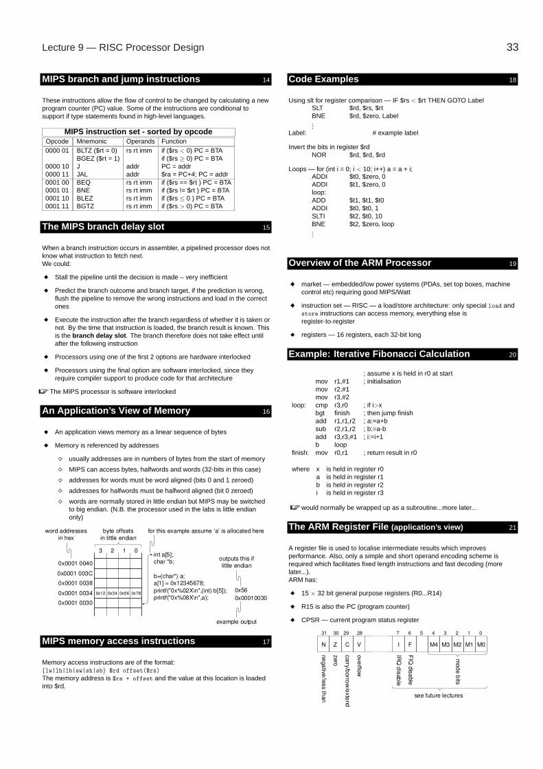
Lecture 9 — RISC Processor Design 33
MIPS branch and jump instructions y 14
These instructions allow the flow of control to be changed by calculating a newprogram counter (PC) value. Some of the instructions are conditional tosupport if type statements found in high-level languages.
MIPS instruction set - sorted by opcodeOpcode Mnemonic Operands Function0000 01 BLTZ ($rt = 0) rs rt imm if ($rs < 0) PC = BTA
BGEZ ($rt = 1) if ($rs ≥ 0) PC = BTA0000 10 J addr PC = addr0000 11 JAL addr $ra = PC+4; PC = addr0001 00 BEQ rs rt imm if ($rs == $rt ) PC = BTA0001 01 BNE rs rt imm if ($rs != $rt ) PC = BTA0001 10 BLEZ rs rt imm if ($rs ≤ 0 ) PC = BTA0001 11 BGTZ rs rt imm if ($rs > 0) PC = BTA
The MIPS branch delay slot y 15
When a branch instruction occurs in assembler, a pipelined processor does notknow what instruction to fetch next.We could:
Stall the pipeline until the decision is made – very inefficient
Predict the branch outcome and branch target, if the prediction is wrong,flush the pipeline to remove the wrong instructions and load in the correctones
Execute the instruction after the branch regardless of whether it is taken ornot. By the time that instruction is loaded, the branch result is known. Thisis the branch delay slot . The branch therefore does not take effect untilafter the following instruction
Processors using one of the first 2 options are hardware interlocked
Processors using the final option are software interlocked, since theyrequire compiler support to produce code for that architecture
The MIPS processor is software interlocked
An Application’s View of Memory y 16
An application views memory as a linear sequence of bytes
Memory is referenced by addresses
usually addresses are in numbers of bytes from the start of memory
MIPS can access bytes, halfwords and words (32-bits in this case)
addresses for words must be word aligned (bits 0 and 1 zeroed)
addresses for halfwords must be halfword aligned (bit 0 zeroed)
words are normally stored in little endian but MIPS may be switchedto big endian. (N.B. the processor used in the labs is little endianonly)
MIPS memory access instructions y 17
Memory access instructions are of the format:{lw|lh|lb|sw|sh|sb} $rd offset($rs)
The memory address is $rs + offset and the value at this location is loadedinto $rd.
Code Examples y 18
Using slt for register comparison — IF $rs < $rt THEN GOTO LabelSLT $rd, $rs, $rtBNE $rd, $zero, Label...
Label: # example label
Invert the bits in register $rdNOR $rd, $rd, $rd
Loops — for (int i = 0; i < 10; i++) a = a + i;ADDI $t0, $zero, 0ADDI $t1, $zero, 0loop:ADD $t1, $t1, $t0ADDI $t0, $t0, 1SLTI $t2, $t0, 10BNE $t2, $zero, loop...
Overview of the ARM Processor y 19
market — embedded/low power systems (PDAs, set top boxes, machinecontrol etc) requiring good MIPS/Watt
instruction set — RISC — a load/store architecture: only special load andstore instructions can access memory, everything else isregister-to-register
registers — 16 registers, each 32-bit long
Example: Iterative Fibonacci Calculation y 20
; assume x is held in r0 at startmov r1,#1 ; initialisationmov r2,#1mov r3,#2
loop: cmp r3,r0 ; if i>xbgt finish ; then jump finishadd r1,r1,r2 ; a:=a+bsub r2,r1,r2 ; b:=a-badd r3,r3,#1 ; i:=i+1b loop
finish: mov r0,r1 ; return result in r0
where x is held in register r0a is held in register r1b is held in register r2i is held in register r3
would normally be wrapped up as a subroutine...more later...
The ARM Register File (application’s view) y 21
A register file is used to localise intermediate results which improvesperformance. Also, only a simple and short operand encoding scheme isrequired which facilitates fixed length instructions and fast decoding (morelater...).ARM has:
15 × 32 bit general purpose registers (R0...R14)
R15 is also the PC (program counter)
CPSR — current program status register

34 Computer Design
Conditionals y 22
Every ARM instruction is conditionally executed according to top 4 conditionflags in the CPSR and the condition field of the instruction:
field code meaning0000 EQ Z set (equal)0001 NE Z clear (not equal)0010 CS C set (unsigned higher or same)0011 CC C clear (unsigned lower)0100 MI N set (negative)0101 PL N clear (positive or zero)0110 VS V set (overflow)0111 VC V clear (no overflow)1000 HI C set and Z clear (unsigned higher)1001 LS C clear and Z set (unsigned lower or same)1010 GE N set and V set, or N clear and V clear (>=)1011 LT N set and V clear, or N clear and V set (<)1100 GT Z clear, and either N set and V set, or N clear and V clear (>)1101 LE Z set, or either N set and V clear, or N clear and V set (<=)1110 AL always — if no condition specified then assume AL1111 NV never
Single Loads and Stores — machine code format y 23
N.B. don’t need to remember ARM instruction formats and mnemonics for theexam!
Single Loads and Stores — assembler format y 24
< LDR|STR > {cond}{B}{T}Rd,< address >where LDR = load
STR = storecond = conditional execution bits
B = if present then byte transferT = if present then write back post-indexing
Rd = destination (LDR) / source (STR) register< address > = one of the following:
PC relative pre-indexed address:< expression > PC+ < expression >
Pre-indexed address (i.e. calculate first and optionally write to Rn):[Rn{, < #expression >}]{!} Rn+ expression with optional write through (!)[Rn, {+/−}Rm{, shift}]{!} Rn+ shifted(Rm) with optional write through (!)
Post-indexed address (i.e. calculate afterwards and write to Rn):[Rn]{, < #expression >} Rn+ expression[Rn], {+/−}Rm{, shift} Rn+ shifted(Rm)
Load and Store Multiple y 25
< LDM |STM > {cond} < FD|ED|FA|EA|IA|IB|DA|DB > Rn{!},< Rlist > {}
where LDM/STM = load/store multiplecond = conditional execution bitsRn = base address register
! = write back< Rlist > = 16 bit register selection field
= load the CPSR along with the PC (user mode) or......force use of the user register bank (more later)
action stack mnemonic alternative mnemonicpre-increment load LDMED LDMIBpost-increment load LDMFD LDMIApre-decrement load LDMEA LDMDBpost-decrement load LDMFA LDMDApre-increment store STMFA STMIBpost-increment store STMEA STMIApre-decrement store STMFD STMDBpost-decrement store STMED STMDA
Register/Memory Swap y 26
Swap a registers with memory:SWP{cond}{B}Rd,Rm, [Rn]
Register Rd is loaded from address [Rn] followed by storing Rm to address[Rn].
where {cond} — is the condition part{B} — if present the swaps bytes, otherwise words
Rm,Rn,Rd — are registers
Data Processing Instructions — operations y 27
Mnemonic ActionAND operand1 AND operand2EOR operand1 EOR operand2 (XOR)SUB operand1 – operand2RSB operand2 – operand1ADD operand1 + operand2ADC operand1 + operand2 + carrySBC operand1 – operand2 + carry – 1RSC operand2 – operand1 + carry – 1TST as AND but results not writtenTEQ as EOR but results not writtenCMP as SUB but results not writtenCMN as ADD but results not writtenORR operand1 OR operand2MOV operand2 (operand1 is ignored)BIC operand1 AND NOT(operand2)MVN NOT(operand2) (operand1 is ignored)
Data Processing Instructions — assembler for-mats y 28
Monadic instructions — MOV and MVN:< opcode > {cond}{S}Rd,< Op2 >
Instructions which do not produce a result but set the condition codes — CMP,CMN, TEQ, TST:
< opcode > {cond}Rn,< Op2 >

Lecture 9 — RISC Processor Design 35
Data Processing Instructions — assembler formatscont... y 29
Dyadic instructions — AND, EOR, SUB, RSB, ADD, ADC, SBC, RSC, ORR,BIC:
< opcode > {cond}{S}Rd,Rn,< Op2 >
where < cond > is the conditional execution part{S} sets condition codes if present
< Op2 > = Rm,< shift > or < #expression >Rd,Rn,Rm are registers
< #expression > is a constant expression< shift > is < shiftname >< register >
or < shiftname > #expressionor RRX (rotate right one bit with extend)
< shiftname > is one of: ASL arithmetic shift leftLSL logical shift left (same as ASL)LSR logical shift rightASR arithmetic shift rightROR rotate right
Multiply and Multiply-Accumulate y 30
Assembler syntax:MUL{cond}{S}Rd,Rm,RsMLA{cond}{S}Rd,Rm,Rs,Rn
where {cond} is the condition part{S} sets the condition codes if present
MUL performs Rd = Rm×RsMLA performs Rd = Rm×Rs+Rn
Branch and Branch with Link Instructions y 31
Assembler syntax:B{L}{cond} < expression >
The < expression > is shifted 2 bits left, sign extended to 32 bits and added tothe PC. This allows PC relative branches to +/− 32 Mbytes.
If the L flag is set then the PC value is written to R14 before the branch takesplace. This allows subroutine calls.
Jumps (none PC relative branches if you like) may be performed by directlywriting to R15 which holds the PC.
Coprocessor Data Operations y 32
Provided by the Coprocessor Data Operation (CDP) instruction which has thefollowing assembler syntax:
CDP{cond} p#, < expression1 >, cd, cn, cm{, < expression2 >}
where {cond} is the usual conditional execution partp# the unique number of the required coprocessor
< expression1 > a constant which represents the coprocessor operandcd, cn and cm are the coprocessor registers
< expression2 > when present provides an extra 3 bits of informationfor the coprocessor
Coprocessor Data Transfers y 33
Provided by a the LDC and STC instructions for loading and storingcoprocessor registers. The address is sourced from the CPU register file butthe other registers refer to the coprocessor.
Assembler syntax:
< LDC|STC > {cond}{L} p#, cd, < address >
where {cond} is the usual conditional execution part{L} transfer length — coprocessor specific meaningp# the unique number of the required coprocessorcd is the coprocessor source or destination register
< address > is one of:< expression > a PC relative address[Rn{, < #expression >}]{!} pre-indexed address[Rn]{, < #expression >} post-indexed address
N.B. see the last lecture for pre and post indexed addressing
Coprocessor Register Transfers y 34
For transferring registers between a coprocessor and the CPU.
Assembler syntax:
< MRC|MCR > {cond} p#, < expression1 >,Rd, cn, cm{, < expression2 >}
where {cond} is the usual conditional execution partp# the unique number of the required coprocessor
< expression1 > a constant which represents the coprocessor operandRd is the CPU source/destination register
cn and cm are the coprocessor registers< expression2 > when present provides an extra 3 bits of information
for the coprocessor
Floating-point Coprocessor y 35
The floating point coprocessor is not supported by the ARM710 but it is byother ARMs. The following mnemonics are converted into the appropriatecoprocessor instructions by the assembler.
ASB absolute value Fd := ABS(Fm)ACS arccosine Fd := ACS(Fm)ADF add floating Fd := Fn + FmASN arcsine Fd := ASN(Fm)ATN arctangent Fd := ATN(Fm)CMF compare floating Flags := (Fn == Fm)CNF compare negative floating Flags := (Fn == –Fm)COS cosine Fd := COS(Fm)DVF divide floating Fd := Fn / FmEXP exponentiation Fd := eFm
FDV fast divide floating Fd := Fn / Fm (single precision)FIX convert float to integer Rd := FIX(Fm)FLT convert integer to float Fd := FLT(Rd)
etc...
Overly complex. Few instructions ever supported by the (slow) floatingpoint coprocessor — the others were handeled as exceptions
36 Computer Design
Code Examples y 36
Using conditional for logical OR — IF Rn=p OR Rm=q THEN GOTO LabelCMP Rn,#pBEQ LabelCMP Rm,#qBEQ Label...
Label: ; example label
May be reduced to:CMP Rn,#pCMPNE Rm,#qBEQ Label
Multiply by 2n, i.e. Rb := Ra× 2n:MOV Rb, Ra, LSL #n
Multiply by 1 + 2n, i.e. Rb := Ra+Ra× 2n:ADD Rb, Ra, Ra, LSL #n
Other ARM instruction sets y 37
This lecture presented the classic 32-bit ARM instruction set
ARM have introduced other instruction sets:
Thumb — their first 16-bit instruction set - better coding density
Thumb2 — a 16-bit and 32-bit instruction set
Jazelle DBX — direct execution of some Java bytecodes (with theother instructions causing traps allowing software to emulate)
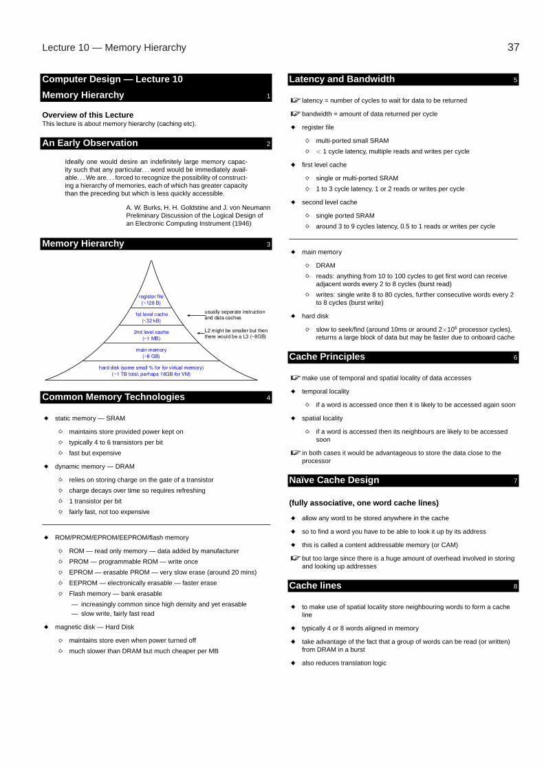
Lecture 10 — Memory Hierarchy 37
Computer Design — Lecture 10
Memory Hierarchy y 1
Overview of this LectureThis lecture is about memory hierarchy (caching etc).
An Early Observation y 2
Ideally one would desire an indefinitely large memory capac-ity such that any particular. . . word would be immediately avail-able. . . We are. . . forced to recognize the possibility of construct-ing a hierarchy of memories, each of which has greater capacitythan the preceding but which is less quickly accessible.
A. W. Burks, H. H. Goldstine and J. von NeumannPreliminary Discussion of the Logical Design ofan Electronic Computing Instrument (1946)
Memory Hierarchy y 3
Common Memory Technologies y 4
static memory — SRAM
maintains store provided power kept on
typically 4 to 6 transistors per bit
fast but expensive
dynamic memory — DRAM
relies on storing charge on the gate of a transistor
charge decays over time so requires refreshing
1 transistor per bit
fairly fast, not too expensive
ROM/PROM/EPROM/EEPROM/flash memory
ROM — read only memory — data added by manufacturer
PROM — programmable ROM — write once
EPROM — erasable PROM — very slow erase (around 20 mins)
EEPROM — electronically erasable — faster erase
Flash memory — bank erasable
— increasingly common since high density and yet erasable— slow write, fairly fast read
magnetic disk — Hard Disk
maintains store even when power turned off
much slower than DRAM but much cheaper per MB
Latency and Bandwidth y 5
latency = number of cycles to wait for data to be returned
bandwidth = amount of data returned per cycle
register file
multi-ported small SRAM
< 1 cycle latency, multiple reads and writes per cycle
first level cache
single or multi-ported SRAM
1 to 3 cycle latency, 1 or 2 reads or writes per cycle
second level cache
single ported SRAM
around 3 to 9 cycles latency, 0.5 to 1 reads or writes per cycle
main memory
DRAM
reads: anything from 10 to 100 cycles to get first word can receiveadjacent words every 2 to 8 cycles (burst read)
writes: single write 8 to 80 cycles, further consecutive words every 2to 8 cycles (burst write)
hard disk
slow to seek/find (around 10ms or around 2×10⁶ processor cycles),returns a large block of data but may be faster due to onboard cache
Cache Principles y 6
make use of temporal and spatial locality of data accesses
temporal locality
if a word is accessed once then it is likely to be accessed again soon
spatial locality
if a word is accessed then its neighbours are likely to be accessedsoon
in both cases it would be advantageous to store the data close to theprocessor
Naıve Cache Design y 7
(fully associative, one word cache lines)
allow any word to be stored anywhere in the cache
so to find a word you have to be able to look it up by its address
this is called a content addressable memory (or CAM)
but too large since there is a huge amount of overhead involved in storingand looking up addresses
Cache lines y 8
to make use of spatial locality store neighbouring words to form a cacheline
typically 4 or 8 words aligned in memory
take advantage of the fact that a group of words can be read (or written)from DRAM in a burst
also reduces translation logic

38 Computer Design
Direct Mapped Cache y 9
use part of the address to map directly onto a cache line so a word canonly live in one place in the cache
Set Associative Cache y 10
direct mapped caches behave badly if data is being used from a range ofaddresses which overlap in the cache
a set associative caches are direct mapped cache but with a set of cachelines at each location
lookup the data in the direct mapped cache and used the appropriate’valid’ tag to indicate which element to read from.
so a word at a particular address can be stored in n places where n is thenumber of elements in a fully associative set (typically n = 2 or 4 butsometimes 64 or more).
Victim Buffer/Cache y
victim buffer — a one line cache line buffer to store the last line overwrittenin the cache
used to augment a direct mapped cache to give it a small amount ofassociativity
victim cache — an extension of the victim buffer idea, a small fullyassiciative cache used in conjunction with a direct mapped cache
Cache Line Replacement PoliciesFor Set Associative Caches y 11
(what to do when the cache is full)
Least Recently Used
good policy but requires usage information to be stored in the cache
Not Last Used
sort of “pass the hot potato”
pass the “potato” on if that cache line is accessed
“potato” tends to come to rest at cache line infrequently used
has a few pathological cases
Random
actually quite simple and works well in practice
Writes to the cache y 12
if data is already in the cache then write over it, otherwise two commonoptions are...
fetch on write
block is first loaded into the cache and the write is performed
write around
if it isn’t in the cache then leave it uncached but write result to thenext level in the memory hierarchy
Write Back & Write Through y 13
(when to write data to next level in the memory hierarchy)
write through or store through
data is written to both the cache and the lower level memory
so if a cache line is replaced, it doesn’t need to be written back to thememory
write through common for multiprocessor computers so that cachecoherency is possible
write back or copy back or store in
data is written to the cache only
data only written to the lower level memory when its cache line isreplaced
a dirty bit may be used to indicate if the cache line has beenmodified, i.e. if it needs to be written back
Write Buffer & Write Merging y 14
writing to lower level memory takes time
to avoid the processor stalling (waiting) a write buffer is used to store a fewwrites
write buffer may also perform write merging
eliminate multiple writes to the same location
merge writes to the same cache line with the hope of performing awrite burst of consecutive words (faster than several single writes)
Virtual & Physically Addressed Caches y 15
address translation takes time and we would rather not introduce the extralatency when reading from the cache
virtual and physical addresses only differ in the upper bits so if the cacheis no bigger than a page then the lower bits of the virtual address aresufficient to access the cache without conflict with the physical address
if the cache is bigger than a virtual page then two alternatives are:
translate virtual to physical and use physical address to access cache(adds latency)
use the virtual address to access the cache, perform addresstranslation concurrently, and compare physical tag with tag in cachememory
— but when two virtual addresses map to the same physicaladdress (e.g. when sharing memory between processes) theymay be mapped to different places in the cache rather than oneas desired
— this is called cache aliasing— up to the OS to ensure it only allocates shared addresses which
do not alias
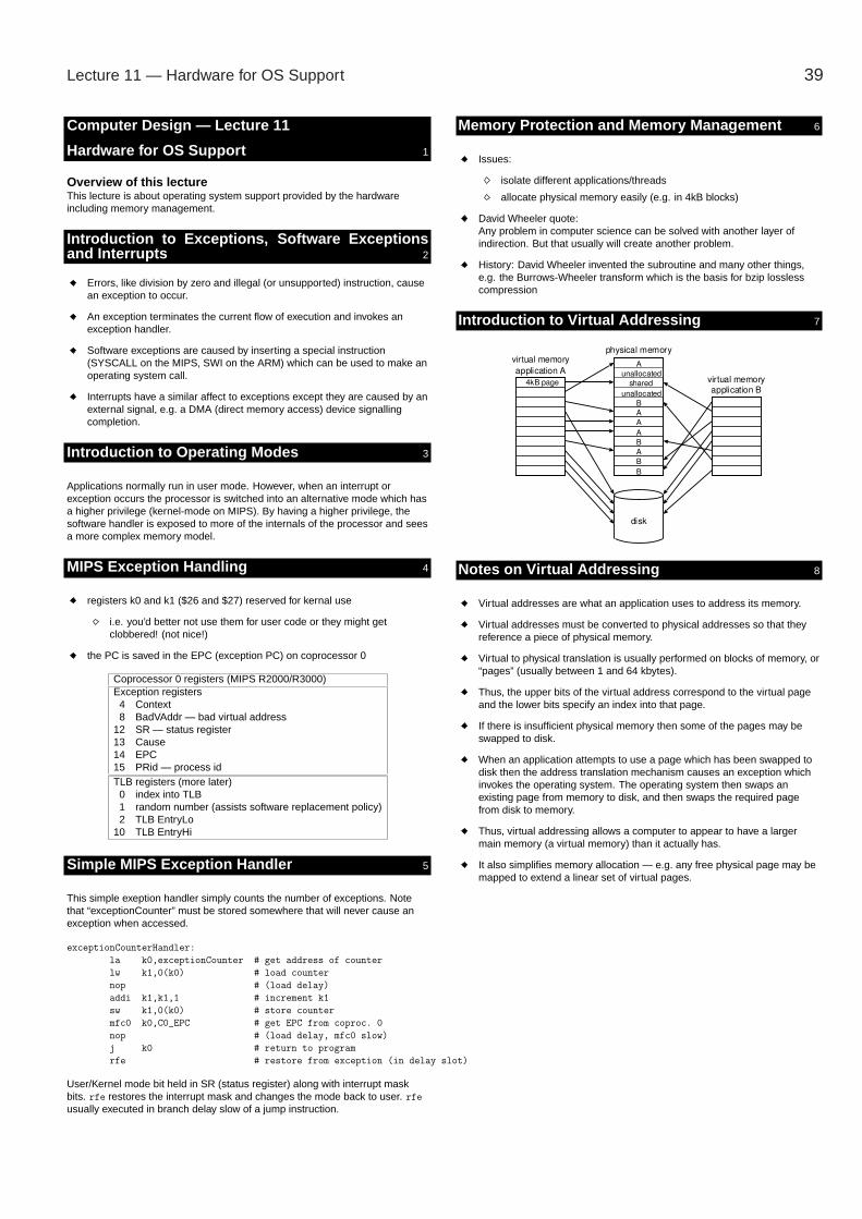
Lecture 11 — Hardware for OS Support 39
Computer Design — Lecture 11
Hardware for OS Support y 1
Overview of this lectureThis lecture is about operating system support provided by the hardwareincluding memory management.
Introduction to Exceptions, Software Exceptionsand Interrupts y 2
Errors, like division by zero and illegal (or unsupported) instruction, causean exception to occur.
An exception terminates the current flow of execution and invokes anexception handler.
Software exceptions are caused by inserting a special instruction(SYSCALL on the MIPS, SWI on the ARM) which can be used to make anoperating system call.
Interrupts have a similar affect to exceptions except they are caused by anexternal signal, e.g. a DMA (direct memory access) device signallingcompletion.
Introduction to Operating Modes y 3
Applications normally run in user mode. However, when an interrupt orexception occurs the processor is switched into an alternative mode which hasa higher privilege (kernel-mode on MIPS). By having a higher privilege, thesoftware handler is exposed to more of the internals of the processor and seesa more complex memory model.
MIPS Exception Handling y 4
registers k0 and k1 ($26 and $27) reserved for kernal use
i.e. you’d better not use them for user code or they might getclobbered! (not nice!)
the PC is saved in the EPC (exception PC) on coprocessor 0
Coprocessor 0 registers (MIPS R2000/R3000)Exception registers
4 Context8 BadVAddr — bad virtual address
12 SR — status register13 Cause14 EPC15 PRid — process idTLB registers (more later)
0 index into TLB1 random number (assists software replacement policy)2 TLB EntryLo
10 TLB EntryHi
Simple MIPS Exception Handler y 5
This simple exeption handler simply counts the number of exceptions. Notethat “exceptionCounter” must be stored somewhere that will never cause anexception when accessed.
exceptionCounterHandler:
la k0,exceptionCounter # get address of counter
lw k1,0(k0) # load counter
nop # (load delay)
addi k1,k1,1 # increment k1
sw k1,0(k0) # store counter
mfc0 k0,C0_EPC # get EPC from coproc. 0
nop # (load delay, mfc0 slow)
j k0 # return to program
rfe # restore from exception (in delay slot)
User/Kernel mode bit held in SR (status register) along with interrupt maskbits. rfe restores the interrupt mask and changes the mode back to user. rfeusually executed in branch delay slow of a jump instruction.
Memory Protection and Memory Management y 6
Issues:
isolate different applications/threads
allocate physical memory easily (e.g. in 4kB blocks)
David Wheeler quote:Any problem in computer science can be solved with another layer ofindirection. But that usually will create another problem.
History: David Wheeler invented the subroutine and many other things,e.g. the Burrows-Wheeler transform which is the basis for bzip losslesscompression
Introduction to Virtual Addressing y 7
Notes on Virtual Addressing y 8
Virtual addresses are what an application uses to address its memory.
Virtual addresses must be converted to physical addresses so that theyreference a piece of physical memory.
Virtual to physical translation is usually performed on blocks of memory, or“pages” (usually between 1 and 64 kbytes).
Thus, the upper bits of the virtual address correspond to the virtual pageand the lower bits specify an index into that page.
If there is insufficient physical memory then some of the pages may beswapped to disk.
When an application attempts to use a page which has been swapped todisk then the address translation mechanism causes an exception whichinvokes the operating system. The operating system then swaps anexisting page from memory to disk, and then swaps the required pagefrom disk to memory.
Thus, virtual addressing allows a computer to appear to have a largermain memory (a virtual memory) than it actually has.
It also simplifies memory allocation — e.g. any free physical page may bemapped to extend a linear set of virtual pages.

40 Computer Design
Simplified View of Address Translation y 9
The big problem is that the translation table must be large. However, it issparse so a more complex data structure will solve the problem.
Translation Look-aside Buffer y 10
We can use a content addressable memory to store address translations -a translation look-aside buffer (TLB).
Translation Look-aside Buffer cont... y 11
But associative TLBs don’t scale so they can only cache recentlyperformed translations so that they may be reused.
Typically TLBs have round 64 to 128 entries.
How do we handle a TLB miss? Hardware? Software?
Address translation — the problem y 12
if we have 4kB pages ⇒ 12 bits for page offset
if we have 32 bit addressing, then the virtual page number is 32− 12 = 20bits
page table has 4 byte word for each entry, so simple page table4× 220 = 4194304 bytes = 4MB memory per table (e.g. per application)
one solution: multilevel page tables (tree structure)
Multilevel Page Tables y 13
Alternative: Inverted Page Tables y 14
have a page table with an entry per physical page
each entry contains: (valid, processes ID, virtual page number)
advantage: compact table
disadvantage: have to search the table to match the virtual address(solutions to this beyond the scope of this course)
Hardware page table walking on ARMs y 15
ARM processors and others (e.g. IA32 and IA64 processors) handle TLBmisses in hardware using page table walking logic.
The ARM710 supports address translation on the following block sizes:
1 Mbyte blocks — sections64 kbyte blocks — large pages16 kbyte blocks — a subpage of a large page4 kbyte blocks — small pages1 kbyte blocks — a subpage of the small page
First Level Fetch y 16
A translation table is provided for each section (1 Mbyte block):
N.B. The translation table base register is set by the operating system on acontext switch.

Lecture 11 — Hardware for OS Support 41
First Level Descriptor y 17
The first level pointer is used as an address to lookup the first level descriptor:
where domain identifies which of the 16 subdomains this belongs toC & B control the cache and write-buffer functions (more later)
AP controls the access permissions — what can be read andwritten in User and Supervisor modes.
Using a Section Base Address y 18
Using a Page Table Base Address y 19
page table base address is prepended with the level 2 (L2) table index toform the second level pointer (see next slide)
the second level pointer is then used to look up the second leveldescriptor:
where C & B control the cache and write-buffer functions (more later)AP0...AP3 controls the access permissions — what can be read and
written in User and Supervisor modes — for the four subpages.
Translating Small Page References y 20
Translating Large Page References y 21
TLB and Memory Protection y 22
A TLB entry not only contains the translation information, but also theprotection data.
Possible exceptions raised:
alignment fault — e.g. attempting to read a 32 bit word from anaddress which is not on a 4 byte boundary
translation fault — a TLB miss occurred and the relevant translationinformation was not present in the translation structure
domain fault — the TLB entry does not have the same subdomain asthe currently executing application
permission fault — the current application does not have the correctread or write permissions to access the page
Memory-Mapped I/O y 23
Input and Output (I/O) devices are usually mapped to part of the addressspace
reading from an I/O device often has side effects, e.g. reading data from aFIFO or reading the status of a device which might then clear the status
memory protection used to ensure that only the device driver has access
device drivers can be in user mode or kernel mode depending on the OS
some processors (notably IA32) have special instructions to access I/Owithin a dedicated I/O address space

42 Computer Design
Single or Multiple Virtual Address Spaces? y 24
There are two principal virtual addressing schemes:
multiple address space — each application resides in its own separatevirtual address space and is prohibited from making accesses outside thisspace.
single address space — there is only one virtual address space and eachapplication being executed is allocated some part of it.
Multiple address maps are often used — e.g. typically supported by UNIX.Linking an application’s components together may be performed statically(pre-run-time). However, sharing libraries and data is more difficult — itinvolves having several virtual addresses for the same physical address.
Single address maps force linking at load time because the exact address ofany particular component is only known then. However, sharing libraries anddata is much simpler — only one virtual address for each physical one —which also makes better use of the TLB (see later).
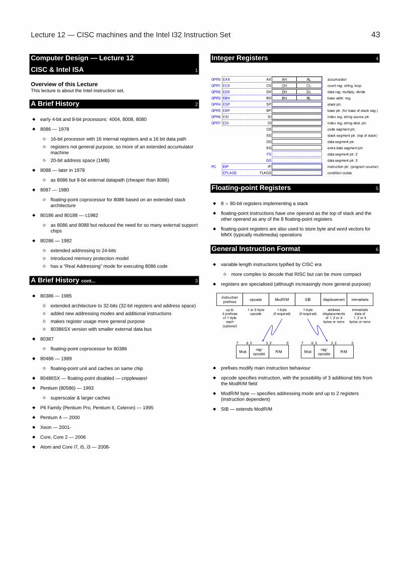
Lecture 12 — CISC machines and the Intel I32 Instruction Set 43
Computer Design — Lecture 12
CISC & Intel ISA y 1
Overview of this LectureThis lecture is about the Intel instruction set.
A Brief History y 2
early 4-bit and 8-bit processors: 4004, 8008, 8080
8086 — 1978
16-bit processor with 16 internal registers and a 16 bit data path
registers not general purpose, so more of an extended accumulatormachine
20-bit address space (1MB)
8088 — later in 1978
as 8086 but 8-bit external datapath (cheaper than 8086)
8087 — 1980
floating-point coprocessor for 8086 based on an extended stackarchitecture
80186 and 80188 — c1982
as 8086 and 8088 but reduced the need for so many external supportchips
80286 — 1982
extended addressing to 24-bits
introduced memory protection model
has a “Real Addressing” mode for executing 8086 code
A Brief History cont... y 3
80386 — 1985
extended architecture to 32-bits (32-bit registers and address space)
added new addressing modes and additional instructions
makes register usage more general purpose
80386SX version with smaller external data bus
80387
floating-point coprocessor for 80386
80486 — 1989
floating-point unit and caches on same chip
80486SX — floating-point disabled — crippleware!
Pentium (80586) — 1993
superscalar & larger caches
P6 Family (Pentium Pro, Pentium II, Celeron) — 1995
Pentium 4 — 2000
Xeon — 2001-
Core, Core 2 — 2006
Atom and Core i7, i5, i3 — 2008-
Integer Registers y 4
Floating-point Registers y 5
8 × 80-bit registers implementing a stack
floating-point instructions have one operand as the top of stack and theother operand as any of the 8 floating-point registers
floating-point registers are also used to store byte and word vectors forMMX (typically multimedia) operations
General Instruction Format y 6
variable length instructions typified by CISC era
more complex to decode that RISC but can be more compact
registers are specialised (although increasingly more general purpose)
prefixes modify main instruction behaviour
opcode specifies instruction, with the possibility of 3 additional bits fromthe ModR/M field
ModR/M byte — specifies addressing mode and up to 2 registers(instruction dependent)
SIB — extends ModR/M
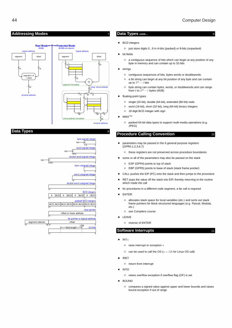
44 Computer Design
Addressing Modes y 7
Data Types y 8
Data Types cont... y 9
BCD integers
just store digits 0...9 in 4-bits (packed) or 8-bits (unpacked)
bit fields
a contiguous sequence of bits which can begin at any position of anybyte in memory and can contain up to 32-bits
strings
contiguous sequences of bits, bytes words or doublewords.
a bit string can begin at any bit position of any byte and can containup to 232 − 1 bits
byte string can contain bytes, words, or doublewords and can rangefrom 0 to 232 − 1 bytes (4GB)
floating-point types
single (32-bit), double (64-bit), extended (80-bit) reals
word (16-bit), short (32-bit), long (64-bit) binary integers
18 digit BCD integer with sign
MMXTM
packed 64-bit data types to support multi-media operations (e.g.JPEG)
Procedure Calling Convention y 10
parameters may be passed in the 6 general purpose registers(GPR0,1,2,3,6,7)
these registers are not preserved across procedure boundaries
some or all of the parameters may also be passed on the stack
ESP (GPR4) points to top of stack
EBP (GPR5) points to base of stack (stack frame pointer)
CALL pushes the EIP (PC) onto the stack and then jumps to the procedure
RET pops the value off the stack into EIP, thereby returning to the routinewhich made the call
for procedures in a different code segment, a far call is required
ENTER
allocates stack space for local variables (etc.) and sorts out stackframe pointers for block structured languages (e.g. Pascal, Modula,etc.)
see Compilers course
LEAVE
reverse of ENTER
Software Interrupts y 11
INTn
raise interrupt or exception n
can be used to call the OS (n = 128 for Linux OS call)
IRET
return from interrupt
INTO
raises overflow exception if overflow flag (OF) is set
BOUND
compares a signed value against upper and lower bounds and raisesbound exception if out of range
Lecture 12 — CISC machines and the Intel I32 Instruction Set 45
AMD64 vs. Intel 64 war y 12
Intel heading for new ISA incompatible with IA32: IA64
AMD introduced 64-bit extension to IA32 and won!
Intel played catch-up with Intel 64 (sometimes called x64)
Intel 64 y 13
64-bit flat linear addressing
no segment registers in 64-bit mode
old CS, DS, ES and SS segment registers treated as being zero
64-bit wide resiters and instruction pointers
8 additional general-purpose registers
8 additional registers for streaming extensions
new instruction-pointer relative-addressing mode
compatability mode for IA32 applications
Intel Instruction Set Summary y 14
full document available from:http://www.intel.com/content/www/us/en/processors/architectures-software-developer-manuals.html

46 Computer Design
Lecture 13 — Java Virtual Machine 47
Computer Design — Lecture 13
The Java Virtual Machine y 1
Overview of this LectureThis lecture gives a taste of the Java Virtual Machine Architecture
Introduction y 2
the Java Virtual Machine (JVM) is a (virtual) processor specification forrunning Java programs
JVM programs are typically executed by a Java interpreter
or can be code converted to run directly on another processor
– or a combination of the two with a Just In Time (JIT) compiler
or executed by a Java Processor
– may be slower than code converting to a register machine!
instruction set architecture is stack based with variable length byte codeinstructions
Why use virtual machines?
→ virtual machines (abstract machine for which an interpreter exists) allowsportability
compile to an interpretive code
porting to new architecture requires writing new interpreter which is(usually) easier than rewriting the back end to the compiler
also allows just one binary to be shipped for all architectures
A Brief History of Portable Interperative Codes y 3
not a new idea — a few examples (dates approximate):
1960 Redcode — used to play Core War (originally “Darwin”)on MARS (Memory Array Redcode Simula-tor)
1961 Algol intermediate code1971 OCODE — by Martin Richards for BCPL (more recently,
Cintcode and Mintcode)1976 P-Code — intermediate code produced by the Pascal-
P compiler (later used by UCSD P-system)1982 PSL — Portable Standard Lisp from University Utah1992 POPLOG — multi-language programming environment
developed at the University of Sussex1995 Java VM — virtual machine for Java
Primative Data Types y 4
byte — 1-byte signed 2’s complement integershort — 2-byte signed 2’s complement integerint — 4-byte signed 2’s complement integerlong — 8-byte signed 2’s complement integerfloat — 4-byte IEEE 754 single-precision floatdouble — 8-byte IEEE 754 double-precision floatchar — 2-byte unsigned Unicode characterobject — 4-byte reference to a Java objectreturnAddress — 4 byte subroutine return address
Registers y 5
the JVM has 4 special purpose registers:
PC — program counter containing the address of the next bytecodeto be executed
vars — register holding base address of memory where localvariables are held
optop — register holding address of top of operand stack
frame — register holding address of base of current frame (holdsenvironment data)
Frames y 6
A frame is used to hold data for a method being executed
contains local variables, operand stack and other run time data
created dynamically each time a method is invoked, and is garbagecollected when the method terminates
Operand Stack y
used to hold intermediate results (instead of using a register file)
JVM Instructions — Genral Format y 7
opcodeoperand 1operand 2
...
first byte = opcode = 8-bit number of instruction
subsequent n bytes are operands (in big endian format), where n can bedetermined from the instruction
JVM Instructions — Arithmetic Instructions y 8
all take one or two operands of the stack and replace with the result
96 iadd Integer add97 ladd Long integer add98 fadd Single floats add99 dadd Double float add100 isub Integer subtract101 lsub Long integer subtract102 fsub Single float subtract103 dsub Double float subtract104 imul Integer multiply105 lmul Long integer multiply106 fmul Single float multiply107 dmul Double float multiply108 idiv Integer divide109 ldiv Long integer divide110 fdiv Single float divide111 ddiv Double float divide112 irem Integer remainder113 lrem Long integer remainder114 frem Single float remainder115 drem Double float remainder116 ineg Integer negate117 lneg Long integer negate118 fneg Single float negate119 dneg Double float negate
similarly for logical operations (AND, OR, NOT, shifts, etc.)
JVM Instructions — Stack Manipulation y 9
0 nop Do nothing87 pop Pop top stack word88 pop2 Pop 2 top stack words89 dup Duplicate top stack word92 dup2 Duplicate top 2 stack words90 dup x1 Duplicate top stack word and put 2 down†93 dup2 x1 Duplicate top 2 stack words and put 2 down91 dup x2 Duplicate top stack word and put 3 down94 dup2 x2 Duplicate top 2 stack words and put 3 down95 swap Swap top 2 stack words
† where put n down means insert the value n places into the stack, e.g.dup x1 does:
..., value2, value1 ⇒ ..., value1, value2, value1

48 Computer Design
JVM Instructions — Jumps, etc. (incomplete) y 10
conditional (if required) is popped off the stack
most branches are 16 bit indicies relative to the PC
153 ifeg Branch if equal (i.e. value popped is zero)154 ifne Branch if not equal (i.e. value! =0)155 iflt Branch if less than (i.e. value<0)156 ifge Branch if greater or equal to (i.e. value>=0)157 ifgt Branch if greater than (i.e. value>0)158 ifle Branch if less than or equal (i.e. value<=0)159 if icmpeq Branch if top 2 items of the stack are equal160 if icmpne Branch if top 2 items of the stack are not equal161 if icmplt Branch if top 2 items of the stack are less than162 if icmpge Branch if top 2 items of the stack are greater or equal163 if icmpgt Branch if top 2 items of the stack are greater than164 if icmple Branch if top 2 items of the stack are less or equal198 ifnull Branch if null (i.e. value popped is null ref to object)199 ifnonnull Branch if not null (i.e. value popped is a ref to object)167 goto Unconditional jump200 goto w Unconditional jump to 32-bit offset168 jsr Jump subroutine, return address pushed on stack201 jsr w As jsr but 32-bit offset169 ret Return from subroutine209 ret w As ret but 32-bit offset
JVM Instructions — Objects and Arrays y 11
object management (complex):
new — create a new object (memory allocation, etc.)
checkcast — make sure object can be converted to a given type
instanceof — determine if an object is of a given type
managing arrays:
newarray, anewarray, multianewarray — array creation
arraylength — array size
iaload, laload, faload, daload, aaload, baload, caload, saload — extractitem from an array
iastore, lastore, fastore, dastore, aastore, bastore, castore, sastore —save item in an array
JVM Instructions — Miscellaneous y 12
return values function (ireturn, lreturn, freturn, dreturn, areturn, return) allpush return values of a particular type onto stack in previous frame(caller’s frame)
tableswitch — long variable length instruction which takes the form:
tableswitch default offset low value high value
array of jump offsets
which pops an index off the stack and does the following:
if((index<low_value) || (index>high_value))
goto default_offset
else
goto array_of_jump_offsets[index]
lookupswitch — similar to tableswitch but jump table is indexedassociatively
manipulating object fields — putfield, getfield, putstatic, getstatic (don’tworry about details!)
method invokation — invokevirtual, invokenonvirtual, invokestatic,invokeinterface
exception handling — athrow
concurrency control — monitorenter, monitorexit
Example Fibonacci Program in Java y 13
class Fib {
public static void main(String[] args) {
for(int i = 0; i<10; i++)
System.out.println("Fib(" + i + ") = " + fib(i));
}
static public int fib(int n) {
if(n<2)
return 1;
else
return fib(n-1)+fib(n-2);
}
}
compile using ‘javac Fib.java’ and disassemble using ‘javap -c Fib’ (e.g. onLinux part of Thor — belt or gloves)
Disassembly y 14
Compiled from Fib.java
synchronized class Fib extends java.lang.Object
/* ACC_SUPER bit set */
{
public static void main(java.lang.String[]);
public static int fib(int);
Fib();
}
Method void main(java.lang.String[])
0 iconst_0
1 istore_1
2 goto 42
5 getstatic #13 <Field java.io.PrintStream out>
8 new #6 <Class java.lang.StringBuffer>
11 dup
12 ldc #2 <String "Fib(">
14 invokespecial #9 <Method java.lang.StringBuffer(java.lang.String)>
17 iload_1
18 invokevirtual #10 <Method java.lang.StringBuffer append(int)>
21 ldc #1 <String ") = ">
23 invokevirtual #11 <Method java.lang.StringBuffer append(java.lang.String)>
26 iload_1
27 invokestatic #12 <Method int fib(int)>
30 invokevirtual #10 <Method java.lang.StringBuffer append(int)>
33 invokevirtual #15 <Method java.lang.String toString()>
36 invokevirtual #14 <Method void println(java.lang.String)>
39 iinc 1 1
42 iload_1
43 bipush 10
45 if_icmplt 5
48 return
Disassembly cont... y 15
Method int fib(int)
0 iload_0
1 iconst_2
2 if_icmpge 7
5 iconst_1
6 ireturn
7 iload_0
8 iconst_1
9 isub
10 invokestatic #12 <Method int fib(int)>
13 iload_0
14 iconst_2
15 isub
16 invokestatic #12 <Method int fib(int)>
19 iadd
20 ireturn
Method Fib()
0 aload_0
1 invokespecial #8 <Method java.lang.Object()>
4 return

Lecture 13 — Java Virtual Machine 49
Resources y 16
Java virtual machine:
http://www.cl.cam.ac.uk/javadoc/vmspec/
Miscellaneous — Free Online Dictionary of Computing (FOLDOC):
http://wombat.doc.ic.ac.uk/foldoc/

50 Computer Design
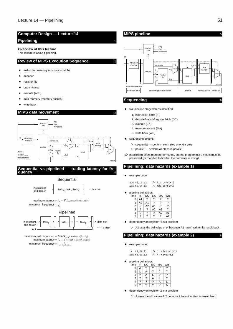
Lecture 14 — Pipelining 51
Computer Design — Lecture 14
Pipelining y 1
Overview of this lectureThis lecture is about pipelining.
Review of MIPS Execution Sequence y 2
instruction memory (instruction fetch)
decoder
register file
branch/jump
execute (ALU)
data memory (memory access)
write back
MIPS data movement y 3
Sequential vs pipelined — trading latency for fre-quency y 4
Sequential
maximum latency = ℓs =∑
2
i=0maxtime(taski)
maximum frequency = 1ℓs
Pipelined
maximum task time = mt = MAX2
i=0maxtime(taski)maximum latency = ℓp = 3× (mt+ latch time)
maximum frequency = 1mt+latch time
MIPS pipeline y 5
Sequencing y 6
five pipeline stages/steps identified:
1. instruction fetch (IF)
2. decode/branch/register fetch (DC)
3. execute (EX)
4. memory access (MA)
5. write back (WB)
sequencing options:
sequential — perform each step one at a time
parallel — perform all steps in parallel
parallelism offers more performance, but the programmer’s model must bepreserved (or modified to fit what the hardware is doing)
Pipelining: data hazards (example 1) y 7
example code:
add t4,t1,t2 // A1: t4=t1+t2
add t5,t4,t3 // A2: t5=t4+t3
pipeline behaviour:time IF DC EX MA WB
0 A1 ? ? ? ?1 A2 A1 ? ? ?2 ? A2 A1 ? ?3 ? ? A2 A1 ?4 ? ? ? A2 A15 ? ? ? ? A2
dependency on register t4 is a problem
A2 uses the old value of t4 because A1 hasn’t written its result back
Pipelining: data hazards (example 2) y 8
example code:
lw t2,0(t1) // L: t2=load(t1)
add t3,t3,t2 // A: t3=t3+t2
pipeline behaviour:time IF DC EX MA WB
0 A ? ? ? ?1 L A ? ? ?2 ? A L ? ?3 ? ? A L ?4 ? ? ? A L5 ? ? ? ? A
dependency on register t2 is a problem
A uses the old value of t2 because L hasn’t written its result back

52 Computer Design
Pipelining: Data hazards (stall) y 9
example code:
add t4,t1,t2 // A1: t4=t1+t2
add t5,t4,t3 // A2: t5=t4+t3
pipeline behaviour with stalls avoid hazards:time IF DC EX MA WB
0 A1 ? ? ? ?1 A2 A1 ? ? ?2 ? A2 A1 ? ?3 ? A2 B A1 ?4 ? A2 B B A15 ? ? A2 B B6 ? ? ? A2 B7 ? ? ? ? A2
A2 stalled at decode stage until result written
no-operations/bubbles (B) inserted into pipeline
bubbles reduce performance
Pipelining: Data hazards (forwarding) y 10
• forwarding (or bypass) paths added to get the result to the execute stagefaster
Pipelining: Stall still required for load y 11
example code:
lw t2,0(t1) // L: t2=load(t1)
add t3,t3,t2 // A: t3=t3+t2
pipeline behaviour:time IF DC EX MA WB
0 A ? ? ? ?1 L A ? ? ?2 ? A L ? ?3 ? A B L ?4 ? ? A B L5 ? ? ? A B6 ? ? ? ? A
stall still required to allow L instruction to complete
forwarding reduces bubbles from 2 to 1
load is said to have one load delay slot for this pipeline
Hardware vs Software Interlocks y 12
hardware interlocks (common approach)
preserve a simple sequential programming model, but add complexityto the control logic (hardware)
a score board can be used to indicate availability of data items
– one bit flag per register indicating if the register is available– load instructions clear the destination register flag during decode
& set the flag again during memory access
software interlocks
expose the load delay slot to the programmer/compiler
simple sequential programmer’s model is not preserved
problem: architecturally dependent, so code is not portable betweenarchitectures unless you preserve the old pipeline model
hardware interlocks usually used, but compiler needs to optimise code toavoid triggering hardware interlock stalls to get max. performance
Microprocessor without InterlockedPipeline Stages y 13
“MIPS” (as in the MIPS architecture) comes from “Microprocessor withoutInterlocked Pipeline Stages”
originally all hazards were to be resolved in software
branch delay slots exposed but load delay slots are not on latermachines
hardware interlocks on result of mul or div allow for differentimplementations of these functions to trade area for performance
some compilers for MIPS (e.g. gcc for MIPS) optionally allows you toenable or disable software resolution of hazards (e.g. branch delayslots) depending upon the amount of hardware support
Note that “MIPS” is also used in computer architecture to mean “Millions ofInstructions Per Second” (just to add to the confusion!)
Control Hazards (branch delay slots) y 14
example code:
j label // J: jump to label
add t3,t1,t2 // A1: t3=t1+t2
label: add t6,t4,t5 // A2: t6=t4+t5
pipeline behaviour:time IF DC EX MA WB
0 J ? ? ? ?1 A1 J ? ? ?2 A2 A1 B ? ?3 ? A2 A1 B ?4 ? ? A2 A1 B5 ? ? ? A2 A16 ? ? ? ? A2
problem: jump/branch taken in DC (then converted into a bubble (B)), butA1 already fetched
solution 1: flush A1 from the pipeline (convert to a bubble)
solution 2: execute A1 anyway (i.e. expose the branch delay slot)
MIPS uses option 2 (i.e. it has branch delays slots)
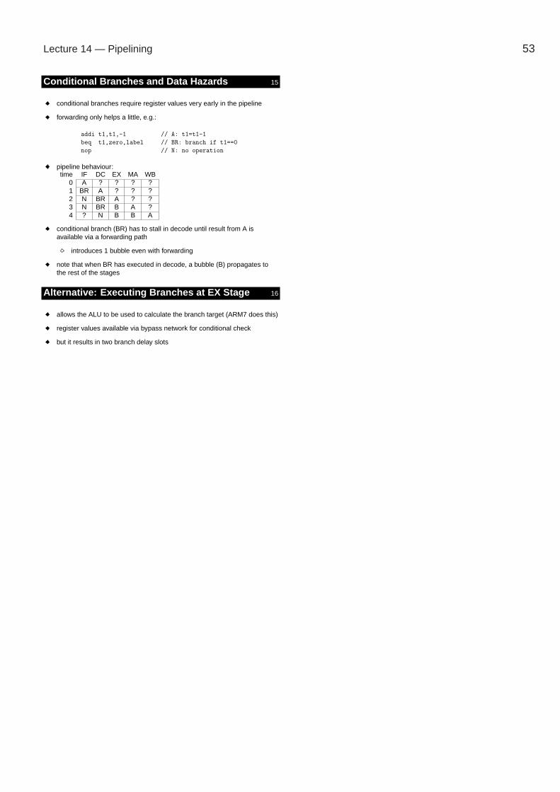
Lecture 14 — Pipelining 53
Conditional Branches and Data Hazards y 15
conditional branches require register values very early in the pipeline
forwarding only helps a little, e.g.:
addi t1,t1,-1 // A: t1=t1-1
beq t1,zero,label // BR: branch if t1==0
nop // N: no operation
pipeline behaviour:time IF DC EX MA WB
0 A ? ? ? ?1 BR A ? ? ?2 N BR A ? ?3 N BR B A ?4 ? N B B A
conditional branch (BR) has to stall in decode until result from A isavailable via a forwarding path
introduces 1 bubble even with forwarding
note that when BR has executed in decode, a bubble (B) propagates tothe rest of the stages
Alternative: Executing Branches at EX Stage y 16
allows the ALU to be used to calculate the branch target (ARM7 does this)
register values available via bypass network for conditional check
but it results in two branch delay slots

54 Computer Design
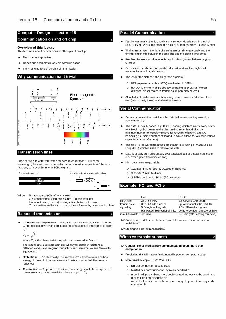
Lecture 15 — Communication on and off chip 55
Computer Design — Lecture 15
Communication on and off chip y 1
Overview of this lectureThis lecture is about communication off-chip and on-chip.
From theory to practise
Trends and examples in off-chip communication
The changing face of on-chip communication
Why communication isn’t trivial y 2
Transmission lines y 3
Engineering rule of thumb: when the wire is longer than 1/100 of thewavelength, then we need to consider the transmission properties of the wire(e.g. any wire over 3mm for a 1GHz signal).
Where: R = resistance (Ohms) of the wireG = conductance (Siemens = Ohm−1) of the insulatorL = inductance (Henries) — magnetism between the wiresC = capacitance (Farads) — capacitance formed by wires and insulator
Balanced transmission y 4
Characteristic impedance — For a loss-less transmission line (i.e. R andG are negligible) which is terminated the characteristic impedance is givenby:
Z0 =√
L
C
where Z0 is the characteristic impedance measured in Ohms.
The model gets a lot more complex when you consider resistance,reflected waves and irregular conductors and insulators — see Maxwell’sequations...
Reflections — An electrical pulse injected into a transmission line hasenergy. If the end of the transmission line is unconnected, the pulse isreflected!
Termination — To prevent reflections, the energy should be dissipated atthe receiver, e.g. using a resistor which is equal to Z0
Parallel Communication y 5
Parallel communication is usually synchronous: data is sent in parallel(e.g. 8, 16 or 32 bits at a time) and a clock or request signal is usually sent
Timing assumption: the data bits arrive almost simultaneously and thetiming relationship between the data bits and the clock is preserved
Problem: transmission line effects result in timing skew between signalson wires
Conclusion: parallel communication doesn’t work well for high clockfrequencies over long distances
The longer the distance, the bigger the problem:
PCI (expansion cards in PCs) was limited to 66MHz
but DDR2 memory chips already operating at 660MHz (shorterdistance, closer matched transmission parameters, etc.)
Also, bidirectional communication using tristate drivers works even lesswell (lots of nasty timing and electrical issues)
Serial Communication y 6
Serial communication serialises the data before transmitting (usually)asynchronously
The data is usually coded, e.g. 8B/10B coding which converts every 8-bitsto a 10-bit symbol guaranteeing the maximum run length (i.e. theminimum number of transitions used for resynchronisation) and DCbalancing (i.e. same number of 1s and 0s which allows for AC coupling viacapacitors or transformers)
The clock is recovered from the data stream, e.g. using a Phase LockedLoop (PLL) which is used to retrieve the data
Data is usually sent differentially over a twisted pair or coaxial connection(i.e. over a good transmission line)
High data rates are possible:
1Gb/s and more recently 10Gb/s for Ethernet
3Gb/s for SATA (to disks)
2.5Gb/s per lane for PCI-e (PCI-express)
Example: PCI and PCI-e y 7
PCI PCI-eclock rate 33 or 66 MHz 2.5 GHz (5 GHz soon)transmission 32 or 64 bits parallel up to 32 serial links 8B/10Bsignalling 5V single rail signals 2.5V differential signals
bus based, bidirectional links point-to-point unidirectional linksmax bandwidth 4.2 Gb/s 64 Gb/s (after coding removed)
So what is the difference between parallel communication and severalserial links?
Striping vs parallel transmission?
Wires vs transistor costs y 8
General trend: increasingly communication costs more thancomputation
Prediction: this will have a fundamental impact on computer design
More trivial example: RS-232 vs USB
simpler connector reduces costs
twisted pair communication improves bandwidth
more intelligence allows more sophisticated protocols to be used, e.g.makes plug-and-play possible(an optical mouse probably has more compute power than very earlycomputers!)
56 Computer Design
RS-232y 9
very old but still commonly used asynchronous serial line standard
electrical:
originally used current-loop signalling
in 1969 the EIA updated to RS-232C which used voltage signalling
with a further update in 1986
but the standard doesn’t specify enough so there are lots of differentRS-232 cables and connectors
protocol:
very simple...
individual wires to report status, e.g. “telephone ringing” (RI)
speed and number of data bits and stop bits set by operator
some more modern devices will auto-detect speed and number ofdata and stop bits
but originally intended for very dumb devices (e.g. electro-mechanicalteletype)
some devices ignore the handshake wires (RTS, CTS, etc) butinstead use a software handshake protocol (ctrl-S to stop data sendand ctrl-Q to restart which are still used on X-terminals, etc.)
RS-232C Pin Definitions y 10
pin numbername 25-pin 9-pin direction functionTD 2 3 out transmitted dataRD 3 2 in received dataRTS 4 7 out request to sendCTS 5 8 in clear to sendDTR 20 4 out data terminal readyDSR 6 6 in data set readyDCD 8 1 in data carrier detectRI 22 9 in ring indicatorFG 1 – frame ground (=chassis)SG 7 5 signal ground
Serial Data Transmission — sending an ’A’ y 11
Here the receiver is recovering the data by oversampling the signal toidentify where the edges are and hence the middle positions of the bits
ASCII code for character A= 6510 = 4116 = 010000012
rising edge of start bit (a logic-0) allows sampling circuit to synchronise
stop bit (a logic-1) ensures that a 0 is always transmitted before the nextstart bit to ensure resynchronisation
if no data is being sent the line remains at logic-1
USBy 12
Universal Serial Bus (USB)
designed to support a range of devices
keyboards, mice, modems, ISDN, audio, slow scanners, printers,interfacing to mobile devices etc.
devices can be chained together
e.g. from computer to keyboard and then to mouse
electrical:
a twisted data pair (bidirectional differential signalling)
power and ground lines to supply power to devices
USB 1.1: 1.5Mb/s slow mode, 12Mb/s full speed
USB 2 added a 480Mb/s mode
protocols:
includes a standard to allow devices to be identified by class, vendor,etc., to allow plug and play
moderately complex initialisation and usage protocols (requiresintelligent devices)
USB on the Desktop y 13
USB Cable and Plugs y 14
A and B plugs ensure star wiring
On-chip communication y 15
Communication on chip has been reasonably easy
lots of wires available
short distances
But wire scaling favours transistors over wires
Moving from bidirectional buses to point-to-point parallel links to switchednetworks

Lecture 15 — Communication on and off chip 57
On-chip bus protocols y 16
Motivation: make it easier to reuse larger hardware components(processors, I/O devices, memories, etc.)
ARM’s AMBA Buses:
ARM’s AMBA Highspeed Bus Architecture (AHB) is widely used
Freely available communications protocol standard
More recently: AXI (AMBA eXtensible Interface)
OpenCores.org:
Wishbone interconnect
Altera buses for their FPGAs:
Avalon — memory communication bus for their NIOS processors andassociated I/O units
Atlantic — point-to-point interfacing of library components
Networks-on-Chip y 17
Challenges:
multiple clock cycle communication latencies
wire reuse to prevent an explosion in wiring complexity
multiple processors, memories and I/O devices on the same chip
On-chip routers are being developed
commercially from Ateris, Sonics Inc., Silistix, ...
lots of research to be done...

58 Computer Design

Lecture 16 — Many-Core 59
Computer Design — Lecture 16
Many-core machines y 1
Overview of this lectureThis lecture reviews parallelism from instruction-level to many-corearchitectures.
Flynn’s Taxonomy of Parallel Architectures y 2
Instruction StreamsData Streams Single Multiple
Single SISD MISDuniprocessor not interesting?
Multiple SIMD MIMDvector processing many core
Instruction Level Parallelism (ILP) y 3
independent instructions can be executed in parallel
e.g. the following instructions have independent destination registers andthe result from the first is not used by the second
add t0,t1,t3
add t4,t2,t3
processors which exploit ILP are often said to be superscalar
programmer’s model is still SISD but some parallelism is extracted
Super Pipelining y 4
execution rate can be increased by making the pipelining more finegrained
also have to pipeline the caches
diminishing returns and increased power
penalty for miss-predicted branch is high
Pentium 4 was probably near the limit with 31 pipeline stages (Cedar Millversion)
Simultaneous Multithreading (SMT) y 5
idea: hold the context (registers/flags) for 2 or more threads in theprocessor and schedule them in hardware
MIMD on one processor
scheduling might interleave instruction issues every cycle
combine with superscalar processing to issue from both threads in thesame cycle
Intel’s name for its version of SMT: hyperthreading — usually just 2threads per CPU
Companion Scheduling y 6
16
4.g
zip
17
5.v
pr
17
6.g
cc
18
1.m
cf
18
6.c
raft
y
19
7.p
ars
er
25
2.e
on
25
3.p
erl
bm
k
25
4.g
ap
25
5.v
ort
ex
25
6.b
zip
2
30
0.t
wo
lf
16
8.w
up
wis
e
17
1.s
wim
17
2.m
gri
d
17
3.a
pp
lu
17
7.m
esa
17
9.a
rt
18
3.e
qu
ake
18
8.a
mm
p
20
0.s
ixtr
ack
30
1.a
psi
164.gzip
175.vpr
176.gcc
181.mcf
186.crafty
197.parser
252.eon
253.perlbmk
254.gap
255.vortex
256.bzip2
300.twolf
168.wupwise
171.swim
172.mgrid
173.applu
177.mesa
179.art
183.equake
188.ammp
200.sixtrack
301.apsi
Speedup > 30%
Speedup 25 to 30%
Speedup 20 to 25%
Speedup 15 to 20%
Speedup 10 to 15%
Speedup 5 to 10%
Approx same
Slowdown 5 to 10%
Slowdown 10 to 15%
Slowdown 15 to 20%
Slowdown > 20%
Figure from James Bulpin’s thesis UCAM-CL-TR-619 — SPEC CPU2000benchmarks running on a Prescott
Companion Scheduling cont... y 7
the good: one thread might run whilst another is waiting for data
e.g. one thread may be waiting on a cache miss but another threadcan be scheduled so the processor is kept busy
i.e. multithreading offers tolerance to memory latencies
results in applications run in parallel completing earlier than if theyhad been run sequentially one after the other
makes more efficient use of the memory system which is really moreimportant than keeping the processor busy
the bad: independent applications/threads compete for resources
e.g. one thread can “pollute” the cached data of another
results in applications running slower in parallel than if they had beenrun sequentially one after the other
the ugly: 3 or more active threads is a bad fit on Prescott
CMP/Multi-Core y 8
CMP = Chip Multi-Processor
MIMD
Multi-Core = Intel’s name for CMP
typical configuration:
currently small numbers of processors with shared L2 or L3 cache
can be combined with SMT/hyperthreading

60 Computer Design
Shared Memory y 9
shared memory ⇒ threads share a coherent view of memory
definition: a memory system is coherent if the results of any execution of aprogram are such that for each location is is possible to construct ahypothetical serial order of all operation to the location that it consistentwith the results of the execution in which:
1. operations issued by any particular process occur in the order issuedby that process, and
2. the value returned by a read is the value written by the last write tothat location in the serial order
two necessary features:
1. write propagation — value written must become visible to others
2. write serialisation — write to location seen in the same order by all
Shared Memory Approaches y 10
simple approach — broadcast writes, e.g. over a shared bus
caches are updated (made coherent) by “snooping” the broadcastdata
clearly doesn’t scale beyond a few (e.g. 4) processors
more complex approach — directory based cache coherency
a directory (e.g. one entry per page) identifies the master writerprocessor and any reader processors
updates are then multicast rather than broadcast
more scalable, but directory still grows linearly with the number ofprocessors + the directory has to be distributed
still results in a lot of memory traffic
more on cache coherency in Comparative Architectures
Shared Memory: Atomic Actions y 11
Need hardware to prove some sort of atomic primitive, e.g.:
test & set
swap
fetch & operation (fetch-and-increment, fetch-and-decrement)
compare and swap
all can be used to provide a locking mechanism used to protect criticalsections
the memory system has to be designed to make these atomic
system-wide atomic operations usually take a significant amount of time
Test and Set Example y 12
Pseudo code:
do {
while(lock != free) { wait(period); } // initial wait
} while(testAndSet(lock) != free); // atomic operation
critical section...
lock = free; // release lock
Notes:
“initial wait” spins looking at the copy of the lock in the processor’scache and waits (e.g. exponential back-off) if the lock is not acquired
“atomic operation” only attempts to acquire the lock if it is likely to befree since the “testAndSet” operation is usually quite expensive
problem: when lock is released and there are N waiting threads thenthere might be as many as N “testAndSet” operations which can beexpensive
Distributed Memory & Message Passing y 13
separate distributed memories are more scalable
e.g. cluster of PCs
communication typically undertaken using message passing
i.e. the programmer has control over the communication complexity
any parallel algorithm can be rewritten to use message passing or sharedmemory, but some algorithms more naturally map to one or the other
MPI & OpenMP y 14
MPI = Message Passing Interface
platform and language independent communication system
see also Open MPI
OpenMP = Open Multi-Processing
used to add parallelism to shared memory systems
consists of a set of compiler directives, library routines, andenvironment variables that influence run-time behaviour
e.g.:
#define N 100000
int main(int argc, char *argv[])
{
int i, a[N];
#pragma omp parallel for
for (i=0;i<N;i++)
a[i]= 2*i;
return 0;
}
Software Approaches y 15
functional parallel
split application up into reasonably separate tasks
e.g. separate rendering from AI engines in gaming
little inter task communication
data parallel
have several threads crawl over a large data set in parallel
e.g. large matrix operations
streamed/software-pipelined
split data processing into a set of steps that can be processed inparallel
stream the data set (and the subsequent intermediate results)through the steps/threads
hybrid — any mixture of the above
see Concurrent Systems course for more details
Lecture 16 — Many-Core 61
Some other companies doing parallel computing y16
XMOS in Bristol have a very low cost 4 processor chips for embeddedapplications. Each processor supports 1 to 8 threads (require 4 or more toget full performance). XC language — cut-down version of C withconcurrency and channel communications added. Rebirth of the InmosTransputer and Occam language (CSP inspired)?
Picochip in Bath — very fine grained processors. Looks more like acourse grained FPGA and is a bit of a nightmare to program.
ARM in Cambridge — a range of processor cores that can be used inCMP configurations.
Broadcom in Cambridge — bought up Alphamosaic (spin out fromCambridge Consultants; a video processing chip for embeddedapplications) and Element-14 (came out of Acorn; Firepath chip for signalprocessing, e.g. DSL line cards).
Tilera in USA — spin-out from MIT; 64 processor chip which looks likes abit like a course grained FPGA.
Sun in USA — T1 and T2 multi-core and multi-threaded processors usedin server environments (SPARC ISA). T1 developed by start-up which wasbought by Sun.
Concluding Remarks y 17
optimum number of threads problem
architecture specific — you usually need as many threads as thehardware can natively support (numberCPUs ×numberHyperthreads)
too many threads and scheduling has to be done by the OS which ispainful
too few threads and you drop performance on the floor
places a large burden on the application writer to write code whichadapts to different platforms
the future
I believe that we need an “infinite” thread model, i.e. the hardwarecan schedule a very large number of threads just like an OS can
the OS then does the out-of-band management (setting prioritylevels, etc.)

62 Computer Design
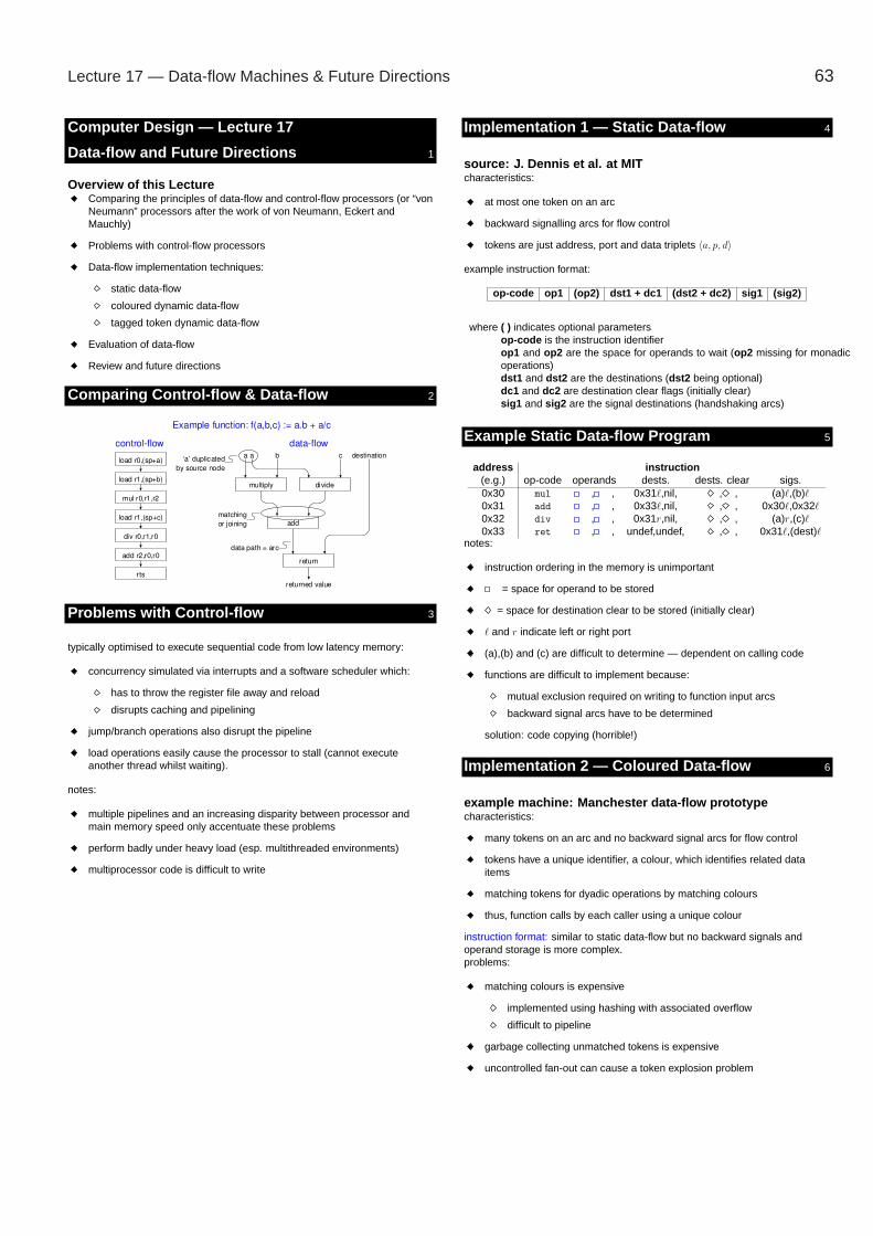
Lecture 17 — Data-flow Machines & Future Directions 63
Computer Design — Lecture 17
Data-flow and Future Directions y 1
Overview of this LectureComparing the principles of data-flow and control-flow processors (or “vonNeumann” processors after the work of von Neumann, Eckert andMauchly)
Problems with control-flow processors
Data-flow implementation techniques:
static data-flow
coloured dynamic data-flow
tagged token dynamic data-flow
Evaluation of data-flow
Review and future directions
Comparing Control-flow & Data-flow y 2
Problems with Control-flow y 3
typically optimised to execute sequential code from low latency memory:
concurrency simulated via interrupts and a software scheduler which:
has to throw the register file away and reload
disrupts caching and pipelining
jump/branch operations also disrupt the pipeline
load operations easily cause the processor to stall (cannot executeanother thread whilst waiting).
notes:
multiple pipelines and an increasing disparity between processor andmain memory speed only accentuate these problems
perform badly under heavy load (esp. multithreaded environments)
multiprocessor code is difficult to write
Implementation 1 — Static Data-flow y 4
source: J. Dennis et al. at MITcharacteristics:
at most one token on an arc
backward signalling arcs for flow control
tokens are just address, port and data triplets 〈a, p, d〉
example instruction format:
op-code op1 (op2) dst1 + dc1 (dst2 + dc2) sig1 (sig2)
where ( ) indicates optional parametersop-code is the instruction identifierop1 and op2 are the space for operands to wait (op2 missing for monadicoperations)dst1 and dst2 are the destinations (dst2 being optional)dc1 and dc2 are destination clear flags (initially clear)sig1 and sig2 are the signal destinations (handshaking arcs)
Example Static Data-flow Program y 5
address instruction(e.g.) op-code operands dests. dests. clear sigs.0x30 mul , , 0x31ℓ,nil, , , (a)ℓ,(b)ℓ0x31 add , , 0x33ℓ,nil, , , 0x30ℓ,0x32ℓ0x32 div , , 0x31r,nil, , , (a)r,(c)ℓ0x33 ret , , undef,undef, , , 0x31ℓ,(dest)ℓ
notes:
instruction ordering in the memory is unimportant
= space for operand to be stored
= space for destination clear to be stored (initially clear)
ℓ and r indicate left or right port
(a),(b) and (c) are difficult to determine — dependent on calling code
functions are difficult to implement because:
mutual exclusion required on writing to function input arcs
backward signal arcs have to be determined
solution: code copying (horrible!)
Implementation 2 — Coloured Data-flow y 6
example machine: Manchester data-flow prototypecharacteristics:
many tokens on an arc and no backward signal arcs for flow control
tokens have a unique identifier, a colour, which identifies related dataitems
matching tokens for dyadic operations by matching colours
thus, function calls by each caller using a unique colour
instruction format: similar to static data-flow but no backward signals andoperand storage is more complex.problems:
matching colours is expensive
implemented using hashing with associated overflow
difficult to pipeline
garbage collecting unmatched tokens is expensive
uncontrolled fan-out can cause a token explosion problem
64 Computer Design
Implementation 3 — Tagged-token Data-flow y 7
example machines: Monsoon machine (MIT) and EM4(Japan)characteristics:
dynamic data-flow, so many tokens per arc
separates the token storage from the program into activation frames(similar to stack frames for a concurrent control-flow program)
function calls generate a new activation frame for code to work in
tokens have an associated activation frame instead of a colour
activation frames are stored in a linear memory with an empty/full flag forevery datum, 〈type, value, port , presence〉
Example Tagged Token andInstruction Formats y 8
example token format:
tag dataframe pointer statement pointer port type value
where frame pointer = address of the start of the activation framestatement pointer = address of the target statement
port = indicates left or right operandtype = integer, floating point etc.
value = typically 64 bits of dataexample instruction format:
op-code (r) dest1 (dest2)
where ( ) indicates optional parametersop-code is the instruction identifierr is the activation frame offset number for dyadic operationsdest1 and dest2 are the destination offsets (dest2 being optional)
Matching Algorithm forDyadic Operations y 9
incoming token’s statement pointer is used to look up the instruction
the instruction’s activation frame offset is added to the token’s activationframe number to give an effective address
the effective address is then used to look up the the presence bit in theactivation frame
if the presence = empty then the token’s value and port are written to thelocation
if the presence = full then the stored value and token value should makeup the two operands for the dyadic instruction (assuming their ports aredifferent)
the operation, its operands and the destination(s) are executednote:
these stages correspond to the stages in the pipeline
Matching Dyadic Operations cont... y 10
Matching Dyadic Operations cont... y 11
Example Tagged-tokenData-flow Program y 12
address instruction(e.g.) op-code offset destinations0x30 mul 0, 0x31ℓ,nil0x31 add 2, 0x33ℓ,nil0x32 div 1, 0x31r,nil0x33 ret 0, (dest)ℓ,nil
note:
ret accepts a 〈destination instruction, port , frame〉 triplet as its leftparameter
advantages:
simple matching algorithm which may be implemented using a pipeline
garbage collecting unmatched tokens is easy
problems:
pipeline bubble every time the first operand of an instruction is matched
token explosion problem can still occur (careful code generation required)
Evaluation of Data-flow y 13
advantages:
inherently concurrent and latency tolerant (no need for caches)
multiprocessor applications are easy to write
disadvantages:
assignment a problem because there is too much concurrency, thusfunctional languages tend to be used. Furthermore, this makes I/O difficult
ineffective use of very local storage (a register file or stack)
scheduling policies have to be simple because of the instruction levelconcurrency
Multithreaded Processors — Combining Control-flow and Data-flow y 14
example machine: Anaconda (Cambridge)
unit of execution is larger so matching time does not dominate
concurrency allows memory latency to be tolerated
Lecture 17 — Data-flow Machines & Future Directions 65
Anaconda — Activation Frame y 15
activation frame maps directly onto the register file:
intermediate results within a microthread use the register file
data between microthreads is passed via the matching store
Anaconda — Architecture Overview y 16
Review and Future Directions y 17
Control-flow has evolved over more than half a century, now with billions ofdollars invested in research.
Data-flow machines are more recent and only prototypes have beenconstructed to date. Results indicate that fine grained data-flow with alarge matching store does not work efficiently
Data-flow ideas now used in today’s superscalar control-flow machines.The register file(s) are effectively matching stores.
We are now in the multicore era, i.e. parallel processing is going to be thenorm not the exception
Challenge: what revolution in computer architecture and language designdo we need to bring parallel programming to the masses?

A Tiny Computer Chuck Thacker, MSR
3 September, 2007
Alan Kay recently posed the following problem:
“I'd like to show JHS and HS kids "the simplest non-tricky architecture" in which simple gates and flipflops manifest a programmable computer”.
Alan posed a couple of other desiderata, primarily that the computer needs to demonstrate fundamental principles, but should be capable of running real programs produced by a compiler. This introduces some tension into the design, since simplicity and performance sometimes are in conflict.
This sounded like an interesting challenge, and I have a proposed design. The machine is a Harvard architecture (separate data and instruction memory) RISC. It executes each instruction in two phases correspond to instruction access and register access and ALU transit. Registers are written at the end of the instruction. Figure 1 is a block diagram of the machine.
Registers
128 X 32
PC
Aout
WD
IM[31:0]
R/W Addr
R Addr
DM[31:0]
doSkip
InData[31:00]
+1
Data Memory
1K X 32
Instruction
Memory
1K X 32
PCmux
0, PCinc
WD
Ph0
IM[31:25]
IM[23:17]
IM[16:10]
WD
W Addr
Aclk
Bclk
Aaddr
Baddr
Waddr
Bout
Skip Test
ALU[31:00]
Ph1
Ph1
Add, Sub, Logic
IM[4:3]
WclkPh0
Ph0
Ph0 Rclk
Wclk
+2
PCinc2
PC
C,N
C,N InRdy
0, IM[23:00]
Jump
LoadConst
In
Load
WriteSelect
doSkip
Jump PCsel
Figure 1: The Tiniest Computer?
IM[9:7]
IM[6:5]Cycle
Ph0
Ph1 Rclk
Wclk
1
Discussion and Implementation
Although it is impractical today to build a working computer with a “handful of gates and flipflops”, it seemed quite reasonable to implement it with an FPGA (field programmable gate array). Modern FPGAs have enormous amounts of logic, as well as a number of specialized “hard macros” such as RAMs. Xilinx sells evaluation boards for about $150 that includes an FPGA and some auxiliary components for connecting the chip to real-world devices and the PC that runs the design tools (which are free to experimenters). This was the approach I took.
Although the machine was designed primarily for teaching, it may have other uses. It is small, fast, and has 32-bit instructions. This may make it competitive with more complex FPGA CPUs. The later section on “Extensions” describes some possibilities for making it a “real” computer (albeit one without Multiply/Divide, Floating Point arithmetic, or virtual memory).
I chose a Harvard architecture because in this arrangement, it is possible to access the data and instruction memories simultaneously. It is still possible to write self-modifying code (although this is usually considered a bad idea), since stores into both memories are supported.
Because it is implemented in the latest generation semiconductor technology (65 nm), the design uses a Xilinx Virtex-5 device. This part has an interesting feature that contributes to the small size of the overall design – a dual-ported static RAM with 1024 words of 36 bits. This RAM is used for the data and instruction memories, and two of them are used to provide the triple-ported register file.
The machine has 32-bit data paths. Most “tiny” computers are 8 or 16 bits wide, but they were designed originally in an era in which silicon was very expensive and package pins were scarce. Today, neither consideration applies. We will implement a variant of the machine with 36-bit data paths.
The design on the instruction set for the machine was determined primarily by the instruction and data path widths. It is a RISC design, since that seemed to be the simplest arrangement from a conceptual standpoint, and it is important to be able to explain the operation clearly.
Although the memories are wide, they are relatively small, containing only 1K locations. The section on extensions discusses some ways to get around this limit. For pedagogical purposes, and for the immediate uses we envision, a small memory seems adequate.
The memory is word-addressed, and all transfers involve full words. Byte addressing is a complexity that was introduced into computers for a number of reasons that are less
2
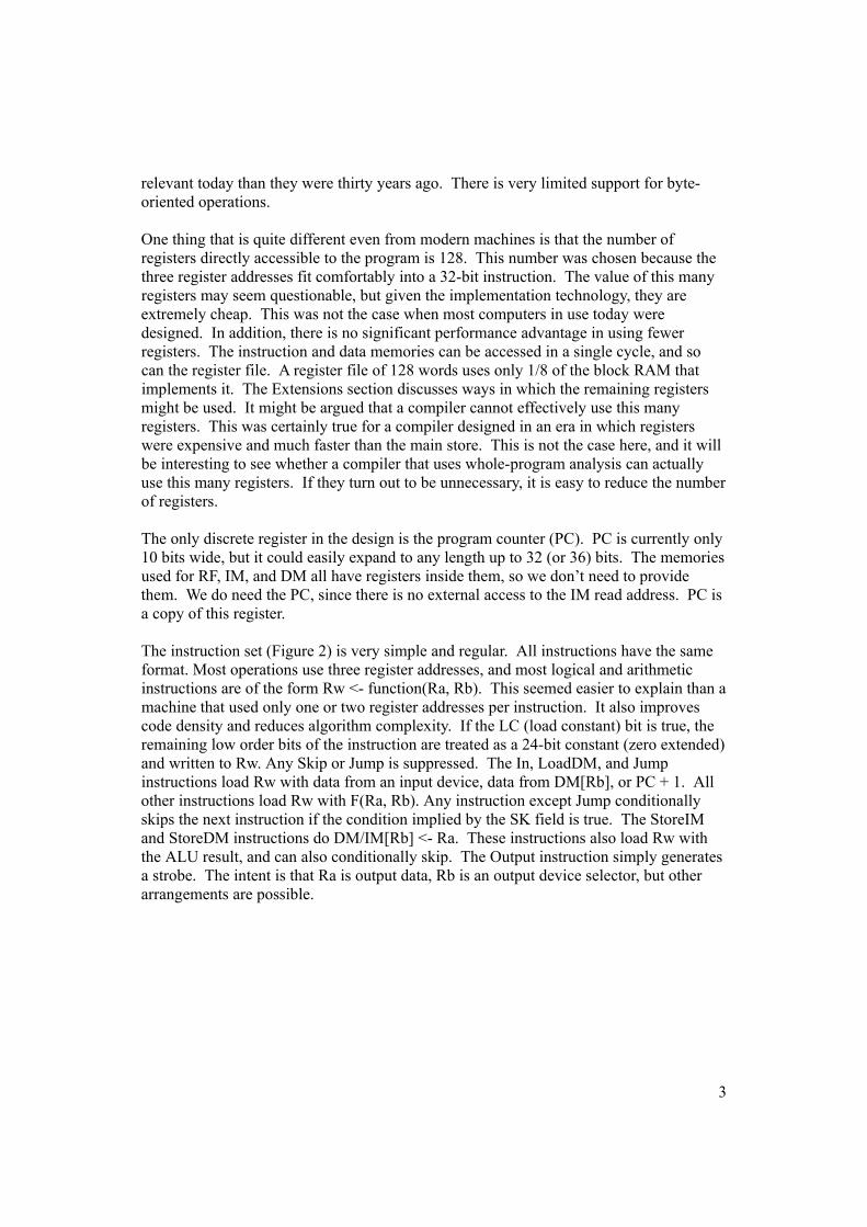
relevant today than they were thirty years ago. There is very limited support for byte-oriented operations.
One thing that is quite different even from modern machines is that the number of registers directly accessible to the program is 128. This number was chosen because the three register addresses fit comfortably into a 32-bit instruction. The value of this many registers may seem questionable, but given the implementation technology, they are extremely cheap. This was not the case when most computers in use today were designed. In addition, there is no significant performance advantage in using fewer registers. The instruction and data memories can be accessed in a single cycle, and so can the register file. A register file of 128 words uses only 1/8 of the block RAM that implements it. The Extensions section discusses ways in which the remaining registers might be used. It might be argued that a compiler cannot effectively use this many registers. This was certainly true for a compiler designed in an era in which registers were expensive and much faster than the main store. This is not the case here, and it will be interesting to see whether a compiler that uses whole-program analysis can actually use this many registers. If they turn out to be unnecessary, it is easy to reduce the number of registers.
The only discrete register in the design is the program counter (PC). PC is currently only 10 bits wide, but it could easily expand to any length up to 32 (or 36) bits. The memories used for RF, IM, and DM all have registers inside them, so we don’t need to provide them. We do need the PC, since there is no external access to the IM read address. PC is a copy of this register.
The instruction set (Figure 2) is very simple and regular. All instructions have the same format. Most operations use three register addresses, and most logical and arithmetic instructions are of the form Rw <- function(Ra, Rb). This seemed easier to explain than a machine that used only one or two register addresses per instruction. It also improves code density and reduces algorithm complexity. If the LC (load constant) bit is true, the remaining low order bits of the instruction are treated as a 24-bit constant (zero extended) and written to Rw. Any Skip or Jump is suppressed. The In, LoadDM, and Jump instructions load Rw with data from an input device, data from DM[Rb], or PC + 1. All other instructions load Rw with F(Ra, Rb). Any instruction except Jump conditionally skips the next instruction if the condition implied by the SK field is true. The StoreIM and StoreDM instructions do DM/IM[Rb] <- Ra. These instructions also load Rw with the ALU result, and can also conditionally skip. The Output instruction simply generates a strobe. The intent is that Ra is output data, Rb is an output device selector, but other arrangements are possible.
3
Rw OpRa Rb Function Shift
Function:
1: A - B
4: A and B
5: A or B
6: A xor B
2: B + 1
3: B - 1
7: Reserved
Shift:
1: RCY 1
2: RCY 8
3: RCY 16
0: A + B
23 417 1031 25 24 016 56 23
Skip
Skip:
0: Never
1: ALU < 0
3: InRdy
2: ALU = 0
Note: If LC, Skip and Jump are suppressed
Figure 2: Instruction Format
0: No shiftLC
9 7
Op:
0: Normal: Rw <- F(Ra, Rb), Skip if condition
7: Reserved
1: StoreDM: DM[Rb] <- Ra, Rw <- F(Ra, Rb), Skip if condition
2: StoreIM: IM[Rb] <- Ra, Rw <- F(Ra, Rb), Skip if condition
4: LoadDM: Rw <- DM[Rb], ALU <- F(Ra, Rb), Skip if condition
3: Out : OutStrobe, Rw <- F(Ra, Rb), Skip if condition
6: Jump: Rw <- PC + 1, PC <- F(Ra, Rb)
5: In: Rw <- InData, ALU <- F(Ra, Rb), Skip if condition
There are relatively few ALU functions. The shifter is placed after the adder/subtractor/logic unit. It too has limited capabilities. If we need more elaborate arithmetic, we can add one or more of Xilinx’ DSP48E cores to the design. These devices are high speed MACs designed for signal processing, but they can do a number of other operations. If we want to avoid DSPs, we need ways to do multiple precision adds and subtracts, multiply, and divide, preferably at one operation per result bit. There are well-known ways to do this while not increasing the complexity too much. But they need more Function and Shift bits to specify them. These could be had by reducing the number of registers to 64, or by increasing all data path widths to 36 bits. The modification needed to support these operations is trivial.
The machine executes instructions in two phases (Ph0 and Ph1). This is unlike essentially all modern computers, which use pipelining to improve performance. The phases are different lengths, since during phase 0, we only need to access the IM, while during phase 1, we must read from the register file, do the ALU operation, and test the result to determine whether the instruction skips. This takes much longer then simply accessing a register. This also makes it much easier to explain how the machine functions. Even with this simplification, the performance is adequate, executing about 60 million instructions per second.
This approach was first employed (I believe) in the original Data General Nova, a simple machine that still has a lot to teach us about computer architecture, since it was arguably the first commercial RISC machine. The major differences are:
(1) There are more registers (128 vs. 4)(2) There are three register select fields instead or two.(3) The Function field has different meanings.(4) The Nova’s Carry field has been eliminated.(5) The Skip field is different. (6) There is no “No load” bit.
4

The Jump instruction saves the (incremented) PC in Rw. This is the only support for subroutines. There is no call stack. Programs that need a stack must construct it themselves.
There is an operation (LC) to load a 24-bit constant (with leading zeros) into Rw. Fabricating constants is usually difficult on a machine with only a few short constants. During an instruction that loads a constant, skips and jumps are suppressed.
There is very little support for input/output. All I/O is programmed, transferring a single 32-bit word between the machine and an external device. There are no interrupts (but see the section on extensions for a possible way of dealing with this). Because the instruction time is completely deterministic, it is easy to write timing-critical programs.
The register addressed by Rw is always written at the end of the instruction. If the value produced is unwanted, Rw should point to a “trashcan” register.
The instruction sequencing of the machine is shown in Figure 3.
Read
IM
Read
RF Write
RF, PC, IM, DM
Phase 0
RF:
IR:
IM:
Ph1:
Phase 1
Ph0:
do ALU op,Skip Test
Phase 0 Phase 1
Figure 3: Instruction Timing
Each instruction requires two phases
During the first phase, IM is first read to retrieve the instruction. At the beginning of phase 1, the RF address register is loaded with the Ra and Rb addresses specified in the instruction. RF is read to retrieve the operands. When RF’s outputs appear, they are passed through the ALU and finally, the register file and PC are written to the register file at the end of the instruction.
The time to read RF (TRCK_DO) plus the time to do an ALU operation and test the result is the reason for the asymmetry, since this is a long combinational path. Phase 0 is approximately of length TRCK_DO + T RCCK_ADDR of the Block RAM, plus wiring delay.
5

The machine is started at Reset by preloading the instruction memory (and if necessary, the data memory) with a bootstrap loader. This is done as part of configuring the FPGA, and the loader is included in the FPGA’s bitstream. The PC is reset to 0, and the loader begins executing. It can load the remainder of the IM and the DM from an I/O device or external RAM/ROM.
Size and Speed
In Virtex-5 technology, the machine occupies about 200 LUTs (lookup tables) and four block RAMs, although a more complex ALU would increase this It runs at 66 MHz, although this could doubtlessly be improved somewhat at the expense of more time spent routing the design. The Verilog describing the entire design is two pages long (Appendix A).
Extensions
The limited size of DM and IM is the main thing that makes this computer noncompetitive. This could be mitigated by using the memories as caches rather than RAM. The 1K BRAM holds 128 eight-word blocks, which is the transfer size of the DRAM controller we are designing for the BEE3. We would need to provide I and D tag stores, but this wouldn’t be very expensive.
For our immediate application, we plan to use the processor to initialize and test two DDR2 memory controllers that connect to two off-FPGA 4 GB DIMMs each (for a total of 16 GB). Each DDR DIMM contains two 2 GB ranks of DRAMs, so there are four ranks per controller. Since these controllers transfer 36 bytes (8 words of 36 bits) in one access, we can use the write port of DM (which is otherwise unused) as the source and destination of DRAM data. To do an operation, the system will load three output registers: A command/rank register containing 3 bits of command, the controller select (1 bit) and the DIMM rank (2 bits), a DRAM address register (31 bits), and the DM address that will supply or receive the data (10 bits). Loading the command starts the transfer, and when it is complete, the data will have been taken from or written to eight successive locations in DM. Completion is tested by testing a “done” flag that is cleared when the command register is loaded, and set when the transfer is complete. As an added feature, we can use the reserved ALU function to generate the next sequence in a prime-polynomial linear feedback shift register. This will be used to generate pseudo-random patterns to test the DIMMs. For this application, the data paths will be increased in width to 36 bits.
The second extension addresses the lack of interrupts. Since the BRAM holding the registers can hold eight full register contexts, it should be straightforward to provide a mechanism similar to that of the Alto. A separate three-bit Context register would hold the current context. Saving and restoring the current context’s PC on a task switch is a bit problematic, but it is probably fairly straightforward.
6

Appendix A: Tiny Computer Verilog description`timescale 1ns / 1ps
module TinyComp(
input Ph0In, Ph1In, //clock phases
input Reset,
input [31:00] InData, // I/O input
input InRdy,
output InStrobe, //We are executing an Input instruction
output OutStrobe //We are executing an Output instruction
);
wire doSkip;
wire [31:00] WD; //write data to the register file
wire [23:00] WDmid; //the WD mux intermediate outputs
wire [31:00] RFAout; //register file port A read data
wire [31:00] RFBout; //register file port B read data
reg [9:0] PC; //10-bit program counter
wire [9:0] PCinc, PCinc2, PCmux;
wire [31:00] ALU; // ALUoutput
wire [31:00] AddSubUnit;
wire [31:00] ALUresult;
wire [31:00] DM; //the Data memory (1K x 32) outputs
wire [31:00] IM; //the Instruction memory (1K x 32) outputs
wire Ph0, Ph1; //the (buffered) clocks
wire WriteIM, WriteDM, Jump, LoadDM, LoadALU; //Opcode decodes
//----------End of declarations------------
//this is the only register, other than the registers in the block RAMs.
// Everything else is combinational.
always @(posedge Ph0)
if(Reset) PC <= 0;
else PC <= PCmux;
// the Phases. They are asymmetric -- see .ucf file
BUFG ph0Buf(.I(Ph0In), .O(Ph0)); //this is Xilinx - specific
BUFG ph1Buf(.I(Ph1In), .O(Ph1));
//the Skip Tester. 1 LUT
assign doSkip = (~IM[24] & ~IM[4] & IM[3] & ALU[31]) |
(~IM[24] & IM[4] & ~IM[3] & (ALU == 0)) |
(~IM[24] & IM[4] & IM[3] & InRdy);
//Opcode decode. 7 LUTs
assign WriteIM = ~IM[24] & ~IM[2] & ~IM[1] & IM[0]; //Op 1
assign WriteDM = ~IM[24] & ~IM[2] & IM[1] & ~IM[0]; //Op 2
assign OutStrobe = ~IM[24] & ~IM[2] & IM[1] & IM[0]; //Op 3
assign LoadDM = ~IM[24] & IM[2] & ~IM[1] & ~IM[0]; //Op 4
assign InStrobe = ~IM[24] & IM[2] & ~IM[1] & IM[0]; //Op 5
assign Jump = ~IM[24] & IM[2] & IM[1] & ~IM[0]; //op 6
assign LoadALU = ~IM[24] & ~IM[2] ; //Ops 0..3
// instantiate the WD multiplexer. 24*2 + 8 = 56 LUTs
genvar i;
generate
for(i = 0; i < 32; i = i+1)
begin: wsblock
if(i < 10 )begin
assign WDmid[i] = (LoadALU & ALU[i]) | (InStrobe & InData[i]) | (LoadDM & DM[i]);
//6-in
assign WD[i] = (Jump & PCinc[i]) | (IM[24] & IM[i]) | WDmid[i]; //5-in
end else if(i < 24) begin
assign WDmid[i] = (LoadALU & ALU[i]) | (InStrobe & InData[i]) | (LoadDM & DM[i]);
//6-in
assign WD[i] = (IM[24] & IM[i]) | WDmid[i]; //3-in
end else
assign WD[i] = (LoadALU & ALU[i]) | (InStrobe & InData[i]) | (LoadDM & DM[i]); //6-in
end //wsblock
endgenerate
//the PC-derived signals
7

assign PCinc = PC + 1;
assign PCinc2 = PC + 2;
assign PCmux = Jump ? ALU[9:0] : doSkip ? PCinc2 : PCinc;
//instantiate the IM. Read during Ph0, written (if needed) at the beginning of the next
Ph0
ramx im(
.clkb(Ph0 ), .addrb(PCmux[9:0]), .doutb(IM), //the read port
.clka(Ph0), .addra(RFBout[9:0]), .wea(WriteIM), .dina(RFAout)); //the write port
//instantiate the DM. Read during Ph1, written (if needed) at the beginning of the next
Ph0
ramx dm(
.clkb(Ph1), .addrb(RFBout[9:0]), .doutb(DM), //the read port
.clka(Ph0), .addra(RFBout[9:0]), .wea(WriteDM), .dina(RFAout)); //the write port
//instantiate the register file. This has three independent addresses, so two BRAMs are
needed.
// read after the read and write addresses are stable (rise of Ph1) written at the end of
the
// instruction (rise of Ph0).
ramx rfA(.addra({3'b0, IM[31:25]}), .clka(Ph0), .wea(1'b0), .dina(WD), //write port
.clkb(Ph1), .addrb({3'b0, IM[23:17]}), .doutb(RFAout)); //read port
ramx rfB(.addra({3'b0, IM[31:25]}), .clka(Ph0), .wea(1'b1), .dina(WD), //write port
.clkb(Ph1), .addrb({3'b0, IM[16:10]}), .doutb(RFBout)); //read port
//instantiate the ALU: An adder/subtractor followed by a shifter
//32 LUTs. IM[8] => mask A, IM[7] => complement B, insert Cin
assign AddSubUnit = ((IM[8]? 32'b0 : RFAout) + (IM[7] ? ~RFBout : RFBout)) + IM[7];
//generate the ALU and shifter one bit at a time
genvar j;
generate
for(j = 0; j < 32; j = j+1)
begin: shblock
assign ALUresult[j] = //32 LUTs
(~IM[9] & AddSubUnit[j]) | //0-3: A+B, A-B, B+1, B-1
( IM[9] & ~IM[8] & ~IM[7] & (RFAout[j] & RFBout[j])) | //4: and
( IM[9] & ~IM[8] & IM[7] & (RFAout[j] | RFBout[j])) | //5: or
( IM[9] & IM[8] & IM[7] & (RFAout[j] ^ RFBout[j])) ; //6: xor
assign ALU[j] = //32 LUTs
(~IM[6] & ~IM[5] & ALUresult[j]) | //0: no cycle
(~IM[6] & IM[5] & ALUresult[(j + 1) % 32]) | //1: rcy 1
( IM[6] & ~IM[5] & ALUresult[(j + 8) % 32]) | //2: rcy 8
( IM[6] & IM[5] & ALUresult[(j + 16) % 32]) ; //rcy 16
end //shblock
endgenerate
endmodule
8

April 2011 Altera Corporation
WP-01149-1.1 White Paper
Subscribe
© 2011 Altera Corporation. All rights reserved. ALTERA, ARRIA, CYCLONE, HARDCOPY, MAX, MEGACORE, NIOS, QUARTUS and STRATIX are Reg. U.S. Pat. & Tm. Off. and/or trademarks of Altera Corporation in the U.S. and other countries. All other trademarks and service marks are the property of their respective holders as described at www.altera.com/common/legal.html. Altera warrants performance of its semiconductor products to current specifications in accordance with Altera’s standard warranty, but reserves the right to make changes to any products and services at any time without notice. Altera assumes no responsibility or liability arising out of the application or use of any information, product, or service described herein except as expressly agreed to in writing by Altera. Altera customers are advised to obtain the latest version of device specifications before relying on any published information and before placing orders for products or services.
101 Innovation Drive
San Jose, CA 95134
www.altera.com
Feedback
Applying the Benefits of Network on aChip Architecture to FPGA System Design
This document describes the advantages of network on a chip (NoC) architecture in Altera® FPGA system design. NoC architectures apply networking techniques and technology to communications subsystems in system on a chip designs. NoC interconnect architectures have significant advantages over traditional, non-NoC interconnects, such as support for independent layer design and optimization. Altera's Qsys system integration tool, included with the Quartus® II software, generates a flexible FPGA-optimized NoC implementation automatically, based on the requirements of the application. The Qsys interconnect also provides a higher operating frequency for comparable latency and resource characteristics, with up to a 2X improvement in fMAX compared to traditional interconnects.
IntroductionAs FPGA device density increases to more than a million logic elements (LEs), design teams require larger and more complex systems, with increasing performance requirements, in less time. Designers can use system-level design tools to quickly design high-performance systems with a minimum of effort.
Qsys uses a NoC architecture to implement system transactions. The Qsys interconnect includes features that support high-performance operation on FPGAs, including a flexible network interconnect that implements only the minimum resources required for a given application, a packet format that varies depending on the system being supported, and a network topology that separates command and response networks for higher concurrency and lower resource utilization.
This white paper explains the Qsys network implementation, discusses its benefits, and compares the performance results between traditional and Qsys interconnect systems. These results show that the NoC implementation provides higher frequency performance with the same latency characteristics, and can provide up to twice the frequency when pipelining options are enabled.
Understanding NoC InterconnectThe NoC interconnect breaks the problem of communication between entities into smaller problems, such as how to transport transactions between nodes in the system, and how to encapsulate transactions into packets for transport. The NoC interconnect is different from traditional interconnects in one simple, but powerful way. Instead of treating the interconnect as a monolithic component of the system, the NoC approach treats the interconnect as a protocol stack, where different layers implement different functions of the interconnect. The power of traditional protocol stacks, such as TCP-over-IP-over-Ethernet, is that the information at each layer is encapsulated by the layer below it. The power of the Qsys NoC implementation comes from the same source, the encapsulation of information at each layer of the protocol stack.
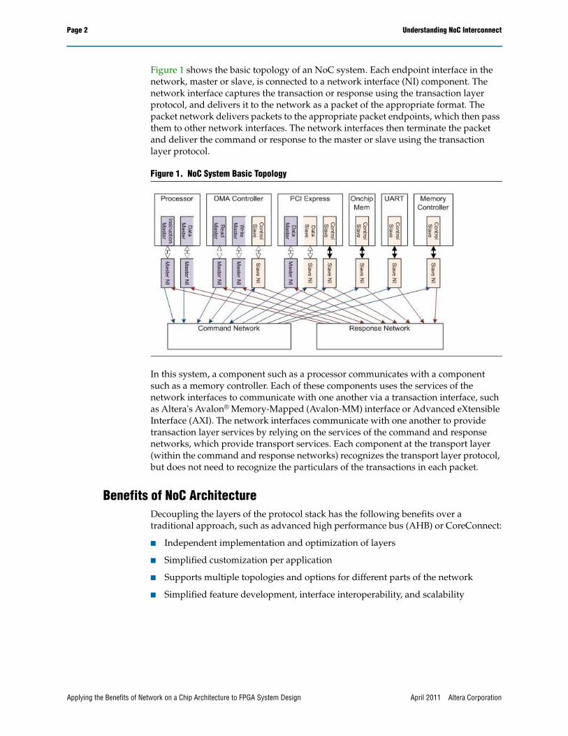
Page 2 Understanding NoC Interconnect
Applying the Benefits of Network on a Chip Architecture to FPGA System Design April 2011 Altera Corporation
Figure 1 shows the basic topology of an NoC system. Each endpoint interface in the network, master or slave, is connected to a network interface (NI) component. The network interface captures the transaction or response using the transaction layer protocol, and delivers it to the network as a packet of the appropriate format. The packet network delivers packets to the appropriate packet endpoints, which then pass them to other network interfaces. The network interfaces then terminate the packet and deliver the command or response to the master or slave using the transaction layer protocol.
In this system, a component such as a processor communicates with a component such as a memory controller. Each of these components uses the services of the network interfaces to communicate with one another via a transaction interface, such as Altera's Avalon® Memory-Mapped (Avalon-MM) interface or Advanced eXtensible Interface (AXI). The network interfaces communicate with one another to provide transaction layer services by relying on the services of the command and response networks, which provide transport services. Each component at the transport layer (within the command and response networks) recognizes the transport layer protocol, but does not need to recognize the particulars of the transactions in each packet.
Benefits of NoC Architecture
Decoupling the layers of the protocol stack has the following benefits over a traditional approach, such as advanced high performance bus (AHB) or CoreConnect:
■ Independent implementation and optimization of layers
■ Simplified customization per application
■ Supports multiple topologies and options for different parts of the network
■ Simplified feature development, interface interoperability, and scalability
Figure 1. NoC System Basic Topology
Understanding NoC Interconnect Page 3
April 2011 Altera Corporation Applying the Benefits of Network on a Chip Architecture to FPGA System Design
Implement and Optimize Layers
A common approach to complex engineering challenges is to divide the design problem into smaller problems with well-defined interactions. With NoC interconnect, the design problem is no longer “How do I best design a flexible interconnect for a complex system?” but instead consists of the easier questions: “How do I best map transactions to packets?” and “How do I best transport packets?” Keeping the layers separate also allows you to optimize the implementation of each layer independently, resulting in better performance at that layer without having to redesign other layers. For example, designers can consider and implement a number of different transport layer topologies and implementations without having to change anything at the transaction layer.
Simplify Customization per Application
At the transport layer, commands and responses are simply packets carried by the network, and anything done at the network layer must only support the transport of these packets. This simplifies the customization of the interconnect for a given application compared to a traditional interconnect. For example, if the designer determines that the system needs pipelining or clock crossing between a set of masters and a set of slaves, the designer can add the needed components as long as they safely transport packets. The clock crossing and pipelining decisions do not need to consider the transaction layer responsibilities, such as the different transaction types, response types, and burst types.
Use Multiple Topologies and Options
NoC interconnect supports use of different optimizations and topologies for different parts of the network. For example, a design may have a set of high-frequency, high-throughput components, such as processors, PCI Express® interfaces, a DMA controller, and memory; and a second set of low-throughput peripherals such as timers, UARTs, flash memory controllers, and I2C interfaces. Such as system can be divided at the transport layer. The designer can place the high-performance components on a wide, high-frequency packet network; while the peripherals are on a less-expensive mesh network, with only a packet bridge between the two networks.
Simplify Feature Development
Interconnects must be versatile enough to support emerging new features, such as new transaction types or burst modes. If the interconnect is divided into different layers, then the addition of new features requires changes only to the layer that supports the feature. To support new burst modes, for example, only the network interface components require modification. Likewise, if a new network topology or transport technology yields higher performance, it can be substituted for the original network without requiring redesign of the entire network.
Interface Interoperability
Different intellectual property (IP) cores support different interface types, such as AMBA® AXI, AHB, and APB interfaces; as well as OCP interfaces, Wishbone interfaces, and Avalon-MM interfaces. Supporting a new interface requires implementing only the network interface to encapsulate transactions to or from interfaces of that type using the selected packet format. With this architecture, a bridge component is not needed, saving logic and latency.
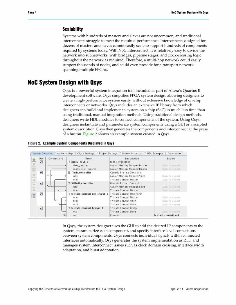
Page 4 NoC System Design with Qsys
Applying the Benefits of Network on a Chip Architecture to FPGA System Design April 2011 Altera Corporation
Scalability
Systems with hundreds of masters and slaves are not uncommon, and traditional interconnects struggle to meet the required performance. Interconnects designed for dozens of masters and slaves cannot easily scale to support hundreds of components required by systems today. With NoC interconnect, it is relatively easy to divide the network into subnetworks, with bridges, pipeline stages, and clock-crossing logic throughout the network as required. Therefore, a multi-hop network could easily support thousands of nodes, and could even provide for a transport network spanning multiple FPGAs.
NoC System Design with QsysQsys is a powerful system integration tool included as part of Altera’s Quartus II development software. Qsys simplifies FPGA system design, allowing designers to create a high-performance system easily, without extensive knowledge of on-chip interconnects or networks. Qsys includes an extensive IP library from which designers can build and implement a system on a chip (SoC) in much less time than using traditional, manual integration methods. Using traditional design methods, designers write HDL modules to connect components of the system. Using Qsys, designers instantiate and parameterize system components using a GUI or a scripted system description. Qsys then generates the components and interconnect at the press of a button. Figure 2 shows an example system created in Qsys.
In Qsys, the system designer uses the GUI to add the desired IP components to the system, parameterize each component, and specify interface-level connections between system components. Qsys connects individual signals within connected interfaces automatically. Qsys generates the system implementation as RTL, and manages system interconnect issues such as clock domain crossing, interface width adaptation, and burst adaptation.
Figure 2. Example System Components Displayed in Qsys
NoC System Design with Qsys Page 5
April 2011 Altera Corporation Applying the Benefits of Network on a Chip Architecture to FPGA System Design
Qsys supports a number of different interface types, such as transaction (read and write) interfaces, streaming (packets or non-packet) interfaces, interrupts, and resets. The Qsys transaction interconnect is based on a NoC implementation that is designed specifically for FPGAs. The Qsys interconnect minimizes the use of FPGA resources, while at the same time supporting high-performance systems with high frequency and throughput requirements.
Qsys NoC Interconnect Optimized for FPGAs
The Qsys NoC interconnect has features that make it particularly well-suited to FPGAs and the systems that use them, including the minimum flexible implementation, parameterizable packet format designed to reduce adaptation, low-latency interconnect, and separate command and response networks.
Minimum, Flexible Implementation
The Qsys interconnect is not just aimed at large high-performance systems with multi-gigabit datapaths and complex bursting, it is also intended for small systems of only a few components. To support such a wide variety of systems, Qsys implements only the minimum interconnect required to meet the performance requirements for a given application.
Qsys begins by dividing the system into multiple interconnect domains. Two interfaces are in different interconnect domains if there are no connections in the system that require the system algorithm to consider them together. For example, if one master connects to two slaves, those slaves are in the same interconnect domain. For each domain, Qsys considers all the master and slave widths, and sets the network data width to be the minimum that supports full throughput for the highest throughput connection in the system, based on the clock rates of the interfaces in the domain.
In addition, Qsys adds only the interconnect components that are required for the application. For example, if there is a master in the system that is only connected to one slave, then the address decoder component is omitted. If there is a slave that is only connected to one master, then the arbiter component is omitted. If a certain type of burst adaptation is not required by that application, then support for that burst adaptation is omitted.
Parameterizable Packet Format Reduces Adaptation
In addition to minimizing interconnect resource use, Qsys determines the packet format that minimizes logic use and adaptation. For example, the address and burstcount fields in the packet are the minimum width required to support the system. The address and other fields within the packet are driven to useful and accurate values in all cycles of the packet, so the adaptation components do not have to maintain any state about the packet, and even allow the adapter to be omitted altogether in some cases.
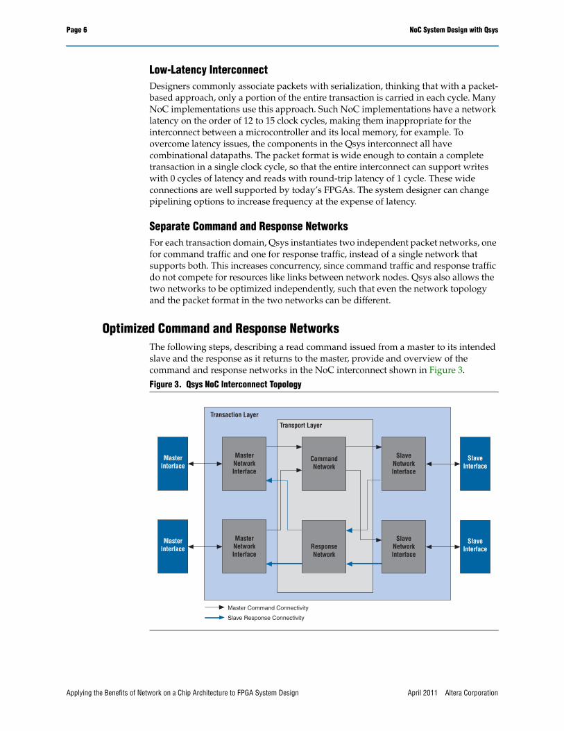
Page 6 NoC System Design with Qsys
Applying the Benefits of Network on a Chip Architecture to FPGA System Design April 2011 Altera Corporation
Low-Latency Interconnect
Designers commonly associate packets with serialization, thinking that with a packet-based approach, only a portion of the entire transaction is carried in each cycle. Many NoC implementations use this approach. Such NoC implementations have a network latency on the order of 12 to 15 clock cycles, making them inappropriate for the interconnect between a microcontroller and its local memory, for example. To overcome latency issues, the components in the Qsys interconnect all have combinational datapaths. The packet format is wide enough to contain a complete transaction in a single clock cycle, so that the entire interconnect can support writes with 0 cycles of latency and reads with round-trip latency of 1 cycle. These wide connections are well supported by today’s FPGAs. The system designer can change pipelining options to increase frequency at the expense of latency.
Separate Command and Response Networks
For each transaction domain, Qsys instantiates two independent packet networks, one for command traffic and one for response traffic, instead of a single network that supports both. This increases concurrency, since command traffic and response traffic do not compete for resources like links between network nodes. Qsys also allows the two networks to be optimized independently, such that even the network topology and the packet format in the two networks can be different.
Optimized Command and Response Networks
The following steps, describing a read command issued from a master to its intended slave and the response as it returns to the master, provide and overview of the command and response networks in the NoC interconnect shown in Figure 3.
Figure 3. Qsys NoC Interconnect Topology
Slave Response Connectivity
Master Command Connectivity
CommandNetwork
Transport Layer
Transaction Layer
Master
NetworkInterface
Master
Interface
SlaveNetworkInterface
SlaveInterface
ResponseNetwork
Master
NetworkInterface
Master
Interface
SlaveNetworkInterface
SlaveInterface
NoC System Design with Qsys Page 7
April 2011 Altera Corporation Applying the Benefits of Network on a Chip Architecture to FPGA System Design
1. When a master issues a command, the first interconnect component that receives the transaction is the translator, as shown in Figure 4. The translator handles much of the variability of the transaction protocol specification, such as active high versus active low signal options and optional read pipelining.
2. The agent is the next block to receive the command. The agent encapsulates the transaction into a command packet, and sends the packet to the command network using the transport layer. The agent also accepts and forwards to the master the response packets from the response network.
3. The router determines the address field within the packet format and the slave ID that the packet goes to, as well as the routing information for the next hop.
4. The limiter tracks outstanding transactions to different masters, and prevents commands resulting in an out-of-order or simultaneously-arriving read response.
5. Next, the component is injected into the packet network. The Qsys NoC network supports maximum concurrency, allowing all masters and slaves to communicate on any given clock cycle, as long as no two masters attempt to access the same slave, as shown in Figure 5.
Figure 4. Master Network Interface
Master
Interface
Master Network Interface
Translator Agent
Router
Limiter
Avalon-STNetwork
(Command)
Avalon-STNetwork
(Response)
Figure 5. Maximum Concurrency Packet Network
Packet Network
Arbiter
Arbiter
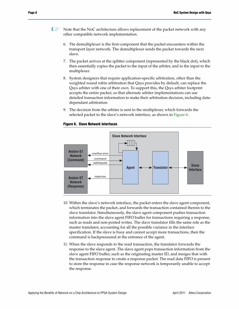
Page 8 NoC System Design with Qsys
Applying the Benefits of Network on a Chip Architecture to FPGA System Design April 2011 Altera Corporation
1 Note that the NoC architecture allows replacement of the packet network with any other compatible network implementation.
6. The demultiplexer is the first component that the packet encounters within the transport layer network. The demultiplexer sends the packet towards the next slave.
7. The packet arrives at the splitter component (represented by the black dot), which then essentially copies the packet to the input of the arbiter, and to the input to the multiplexer.
8. System designers that require application-specific arbitration, other than the weighted round robin arbitration that Qsys provides by default, can replace the Qsys arbiter with one of their own. To support this, the Qsys arbiter footprint accepts the entire packet, so that alternate arbiter implementations can use detailed transaction information to make their arbitration decision, including data-dependant arbitration.
9. The decision from the arbiter is sent to the multiplexer, which forwards the selected packet to the slave’s network interface, as shown in Figure 6.
10. Within the slave’s network interface, the packet enters the slave agent component, which terminates the packet, and forwards the transaction contained therein to the slave translator. Simultaneously, the slave agent component pushes transaction information into the slave agent FIFO buffer for transactions requiring a response, such as reads and non-posted writes. The slave translator fills the same role as the master translator, accounting for all the possible variance in the interface specification. If the slave is busy and cannot accept more transactions, then the command is backpressured at the entrance of the agent.
11. When the slave responds to the read transaction, the translator forwards the response to the slave agent. The slave agent pops transaction information from the slave agent FIFO buffer, such as the originating master ID, and merges that with the transaction response to create a response packet. The read data FIFO is present to store the response in case the response network is temporarily unable to accept the response.
Figure 6. Slave Network Interfaces
SlaveInterface
Slave Network Interface
Agent Translator
waitrequest
overflow error
command
response
Avalon-STNetwork
(Command)
Avalon-STNetwork
(Response)
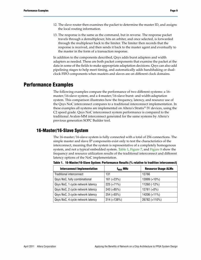
Performance Examples Page 9
April 2011 Altera Corporation Applying the Benefits of Network on a Chip Architecture to FPGA System Design
12. The slave router then examines the packet to determine the master ID, and assigns the local routing information.
13. The response is the same as the command, but in reverse. The response packet travels through a demultiplexer, hits an arbiter, and once selected, is forwarded through the multiplexer back to the limiter. The limiter then records that the response is received, and then sends it back to the master agent and eventually to the master in the form of a transaction response.
In addition to the components described, Qsys adds burst adapters and width adapters as needed. These are both packet components that examine the packet at the data in some of the fields to make appropriate adaptation decisions. Qsys can also add pipelining stages to help meet timing, and automatically adds handshaking or dual-clock FIFO components when masters and slaves are on different clock domains.
Performance ExamplesThe following examples compare the performance of two different systems: a 16-master/16-slave system, and a 4-master/16-slave burst- and width-adaptation system. This comparison illustrates how the frequency, latency, and resource use of the Qsys NoC interconnect compares to a traditional interconnect implementation. In these examples all systems are implemented on Altera's Stratix® IV devices, using the C2 speed grade. Qsys NoC interconnect system performance is compared to the traditional Avalon-MM interconnect generated for the same systems by Altera’s previous generation SOPC Builder tool.
16-Master/16-Slave System
The 16-master/16-slave system is fully connected with a total of 256 connections. The simple master and slave IP components exist only to test the characteristics of the interconnect, meaning that the system is representative of a completely homogenous system, and not a typical embedded system. Table 1, Figure 7, and Figure 8 show the frequency and resource utilization results of the traditional interconnect and different latency options of the NoC implementation.
Table 1. 16-Master/16-Slave System: Performance Results (% relative to tradition interconnect)
Interconnect Implementation fMAX MHz Resource Usage ALMs
Traditional interconnect 131 12766
Qsys NoC, fully combinational 161 (+23%) 13999 (+10%)
Qsys NoC, 1 cycle network latency 225 (+71%) 11260 (-12%)
Qsys NoC, 2 cycle network latency 243 (+85%) 12761 (+0%)
Qsys NoC, 3 cycle network latency 254 (+93%) 14206 (+11%)
Qsys NoC, 4 cycle network latency 314 (+138%) 26782 (+110%)
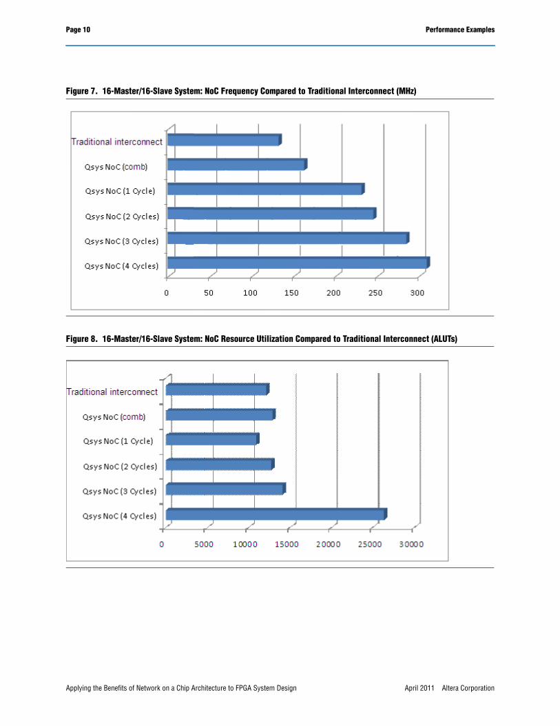
Page 10 Performance Examples
Applying the Benefits of Network on a Chip Architecture to FPGA System Design April 2011 Altera Corporation
Figure 7. 16-Master/16-Slave System: NoC Frequency Compared to Traditional Interconnect (MHz)
Figure 8. 16-Master/16-Slave System: NoC Resource Utilization Compared to Traditional Interconnect (ALUTs)

Performance Examples Page 11
April 2011 Altera Corporation Applying the Benefits of Network on a Chip Architecture to FPGA System Design
4-Master/16-Slave Burst- and Width-Adaptation System
The 4-master/16-slave burst- and width-adaptation system includes characteristics of typical heterogeneous systems, including masters and slaves of different widths and differences in burst support, requiring burst adaptation in the interconnect. Table 2, Figure 9, and Figure 10 show the frequency and resource utilization results of the traditional interconnect and different latency options of the NoC implementation.
Table 2. 4-Master/16-Slave System: Performance Results (% relative to tradition interconnect)
Interconnect Implementation fMAX (MHz) Resource Usage (ALMs)
Traditional interconnect 123 11658
Qsys NoC, fully combinational 125 (+2%) 9655 (-17%)
Qsys NoC, 1 cycle network latency 150 (+22%) 9423 (-19%)
Qsys NoC, 2 cycle network latency 164 (+33%) 9847 (-16%)
Qsys NoC, 3 cycle network latency 154 (+25%) 13156 (+13%)
Qsys NoC, 4cycle network latency 171 (+39%) 16925 (+45%)
Figure 9. 4-Master/16-Slave System: Frequency Compared to Traditional Interconnect (MHz)
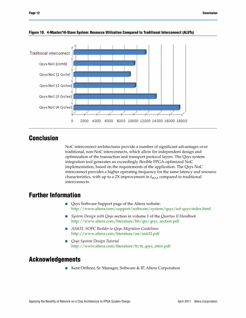
Page 12 Conclusion
Applying the Benefits of Network on a Chip Architecture to FPGA System Design April 2011 Altera Corporation
ConclusionNoC interconnect architectures provide a number of significant advantages over traditional, non-NoC interconnects, which allow for independent design and optimization of the transaction and transport protocol layers. The Qsys system integration tool generates an exceedingly flexible FPGA-optimized NoC implementation, based on the requirements of the application. The Qsys NoC interconnect provides a higher operating frequency for the same latency and resource characteristics, with up to a 2X improvement in fMAX compared to traditional interconnects.
Further Information■ Qsys Software Support page of the Altera website:
http://www.altera.com/support/software/system/qsys/sof-qsys-index.html
■ System Design with Qsys section in volume 1 of the Quartus II Handbookhttp://www.altera.com/literature/hb/qts/qsys_section.pdf
■ AN632: SOPC Builder to Qsys Migration Guidelineshttp://www.altera.com/literature/an/an632.pdf
■ Qsys System Design Tutorialhttp://www.altera.com/literature/tt/tt_qsys_intro.pdf
Acknowledgements■ Kent Orthner, Sr. Manager, Software & IP, Altera Corporation
Figure 10. 4-Master/16-Slave System: Resource Utilization Compared to Traditional Interconnect (ALUTs)
Computer Design Exercises
This set of suggested exercises represents the minimum I would expect completed for supervi-sions. Supervisors are encouraged to set additional material. Suggestions of additional questionswill be gratefully received by the lecturer, as will corrections.
Lectures 1 to 4 – ECAD
• Teach yourself SystemVerilog using the Cambridge SystemVerilog Tutor (CSVT). CSVTteaches you the SystemVerilog you need to complete the ECAD assessed exercises aspainlessly as possible. A number of self-tests check your progress through learningthe basics of the language. The tutorial explains what you need to do to write Sys-temVerilog programs. Link to CSVT via:http://www.cl.cam.ac.uk/Teaching/current/ECAD+Arch/
• Past paper questions on the older ECAD course are generally relevant though they usean older dialect — Verilog 2001.
Lecture 5 — Historical Computer Architecture
• What was Leo and what was it used for?
• Where and when was Whirlwind developed?
• What did TRADIC first demonstrate?
• If memory capacity continues to double every 18 months, how much main memorywill a typical desktop PC have in 20 years time?
Lecture 6 — Early instruction set architecture
• Read and discuss chapters 1 & 2 from “Computer Architecture — A Quantitative Ap-proach” (2nd or 3rd editions, not the most recent), particularly the “fallacies and pit-falls” sections.
Lecture 7 — Thacker’s Tiny Computer 3
• Much of the work for this lecture is in the lab. sessions where you simulate and syn-thesis the design.
• What is the difference between behavioural and structural SystemVerilog design?
• Why is the code density not very good for this processor architecture? (You should beable to answer this once you’ve covered lecture 9 since you can compare instructionsequences with other RISC processors)
Lecture 8 — Systems-on-FPGA Design
• How does a tool like Qsys help to design larger systems-on-FPGA?
Lecture 9 — RISC Processor Design
• Given that the MIPS processor has a branch delay slot, what will the following con-trived piece of code do?
foo: slti $t0, $t0, 5beq $t0, $zero, fooaddi $t0, $t0, -1
• Write a loop that copies a region of memory from the address in $a0 to the addressin $a1 for the number of words specified in $a2. You may assume that the regions ofmemory are none overlapping.
• How might you improve the performance of your code in (b) by copying more thanone word on each iteration of the loop?
• Every ARM instruction is conditional. What had to be sacrificed in order to makespace in the instruction format for the condition code bits?
• Answer past exam. question 2, paper 5, 2004:http://www.cl.cam.ac.uk/tripos/y2004p5q2.pdf

Lecture 10 — Memory Hierarchy
• Read and discuss “Memory Hierarchy Design” from “Computer Architecture — AQuantitative Approach” (2nd or 3rd editions, not the most recent), particularly the“fallacies and pitfalls” sections.
• Answer past exam. question 3, paper 5, 2009:http://www.cl.cam.ac.uk/tripos/y2009p5q3.pdf
Lecture 11 — Hardware for OS Support
• Answer past exam. question 3, paper 5, 2011:http://www.cl.cam.ac.uk/tripos/y2011p5q3.pdf
Lecture 12 — CISC machines and the Intel IA32 Instruction Set
• How did AMD extend Intel’s 32-bit instruction set (IA32) to the 64-bit version AMD64and subsequent Intel 64?
• How does Intel 64 differ from IA64?
Lecture 13 — Java Virtual Machine
• Write an iterative version of Fibonacci in Java and figure out what the disassembledcode means. Run through the code for a fib(4).
Lecture 14 — Pipelining
• Read about pipelining and resolution of hazards, e.g. in Chapter 7 of Harris & Harris,Digital Design and Computer Architecture, 2007.
• Attempt past exam. question 2007 P6 Q2
Lecture 15 — Communication on and off chip
• What is the difference between serial and parallel communication?
• What is the difference between latency and bandwidth?
• What is the difference between a bus and a switched communication network?
• Why is it difficult to communicate data in parallel at GHz frequencies?
Lecture 16 — Manycore
• What is the difference between instruction-level parallelism and thread-level paral-lelism?
• Howdoes SMT exploit both instruction-level parallelism and thread-level parallelism?
• What is companion scheduling?
• What is the difference between manycore and CMP?
Lecture 17 — Data-flow
• What is the difference between data-flow and control-flow?
• Do RISC processors execute instructions in a data-flow or control-flow manner?
• When can modern SMT processors exhibit any data driven behaviour?
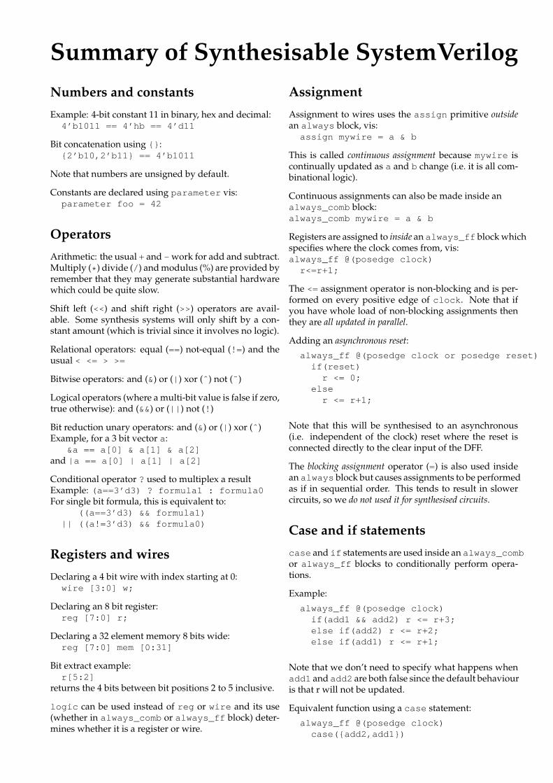
Summary of Synthesisable SystemVerilog
Numbers and constants
Example: 4-bit constant 11 in binary, hex and decimal:4’b1011 == 4’hb == 4’d11
Bit concatenation using {} :{2’b10,2’b11} == 4’b1011
Note that numbers are unsigned by default.
Constants are declared using parameter vis:parameter foo = 42
Operators
Arithmetic: the usual + and - work for add and subtract.Multiply (* ) divide (/ ) andmodulus (%) are provided byremember that they may generate substantial hardwarewhich could be quite slow.
Shift left (<<) and shift right (>>) operators are avail-able. Some synthesis systems will only shift by a con-stant amount (which is trivial since it involves no logic).
Relational operators: equal (==) not-equal (!= ) and theusual < <= > >=
Bitwise operators: and (&) or (| ) xor (ˆ ) not (˜ )
Logical operators (where a multi-bit value is false if zero,true otherwise): and (&&) or (|| ) not (! )
Bit reduction unary operators: and (&) or (| ) xor (ˆ )Example, for a 3 bit vector a:
&a == a[0] & a[1] & a[2]and |a == a[0] | a[1] | a[2]
Conditional operator ? used to multiplex a resultExample: (a==3’d3) ? formula1 : formula0For single bit formula, this is equivalent to:
((a==3’d3) && formula1)|| ((a!=3’d3) && formula0)
Registers and wires
Declaring a 4 bit wire with index starting at 0:wire [3:0] w;
Declaring an 8 bit register:reg [7:0] r;
Declaring a 32 element memory 8 bits wide:reg [7:0] mem [0:31]
Bit extract example:r[5:2]
returns the 4 bits between bit positions 2 to 5 inclusive.
logic can be used instead of reg or wire and its use(whether in always_comb or always_ff block) deter-mines whether it is a register or wire.
Assignment
Assignment to wires uses the assign primitive outsidean always block, vis:
assign mywire = a & b
This is called continuous assignment because mywire iscontinually updated as a and b change (i.e. it is all com-binational logic).
Continuous assignments can also be made inside analways_comb block:always_comb mywire = a & b
Registers are assigned to inside an always_ff blockwhichspecifies where the clock comes from, vis:always_ff @(posedge clock)
r<=r+1;
The <= assignment operator is non-blocking and is per-formed on every positive edge of clock . Note that ifyou have whole load of non-blocking assignments thenthey are all updated in parallel.
Adding an asynchronous reset:
always_ff @(posedge clock or posedge reset)if(reset)
r <= 0;else
r <= r+1;
Note that this will be synthesised to an asynchronous(i.e. independent of the clock) reset where the reset isconnected directly to the clear input of the DFF.
The blocking assignment operator (=) is also used insidean always block but causes assignments to be performedas if in sequential order. This tends to result in slowercircuits, so we do not used it for synthesised circuits.
Case and if statements
case and if statements are used inside an always_combor always_ff blocks to conditionally perform opera-tions.
Example:
always_ff @(posedge clock)if(add1 && add2) r <= r+3;else if(add2) r <= r+2;else if(add1) r <= r+1;
Note that we don’t need to specify what happens whenadd1 and add2 are both false since the default behaviouris that r will not be updated.
Equivalent function using a case statement:
always_ff @(posedge clock)case({add2,add1})
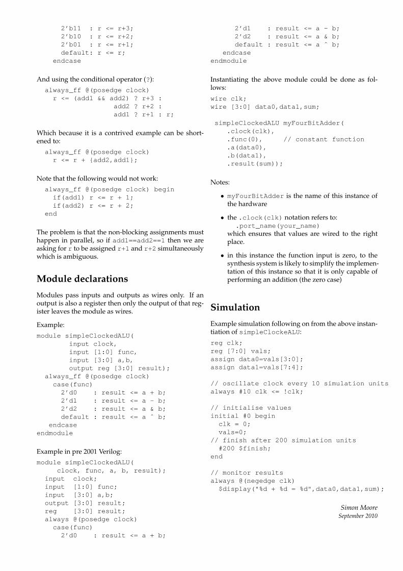
2’b11 : r <= r+3;2’b10 : r <= r+2;2’b01 : r <= r+1;default: r <= r;
endcase
And using the conditional operator (?):
always_ff @(posedge clock)r <= (add1 && add2) ? r+3 :
add2 ? r+2 :add1 ? r+1 : r;
Which because it is a contrived example can be short-ened to:
always_ff @(posedge clock)r <= r + {add2,add1};
Note that the following would not work:
always_ff @(posedge clock) beginif(add1) r <= r + 1;if(add2) r <= r + 2;
end
The problem is that the non-blocking assignments musthappen in parallel, so if add1==add2==1 then we areasking for r to be assigned r+1 and r+2 simultaneouslywhich is ambiguous.
Module declarations
Modules pass inputs and outputs as wires only. If anoutput is also a register then only the output of that reg-ister leaves the module as wires.
Example:
module simpleClockedALU(input clock,input [1:0] func,input [3:0] a,b,output reg [3:0] result);
always_ff @(posedge clock)case(func)
2’d0 : result <= a + b;2’d1 : result <= a - b;2’d2 : result <= a & b;default : result <= a ˆ b;
endcaseendmodule
Example in pre 2001 Verilog:
module simpleClockedALU(clock, func, a, b, result);
input clock;input [1:0] func;input [3:0] a,b;output [3:0] result;reg [3:0] result;always @(posedge clock)
case(func)2’d0 : result <= a + b;
2’d1 : result <= a - b;2’d2 : result <= a & b;default : result <= a ˆ b;
endcaseendmodule
Instantiating the above module could be done as fol-lows:
wire clk;wire [3:0] data0,data1,sum;
simpleClockedALU myFourBitAdder(.clock(clk),.func(0), // constant function.a(data0),.b(data1),.result(sum));
Notes:
• myFourBitAdder is the name of this instance ofthe hardware
• the .clock(clk) notation refers to:.port_name(your_name)
which ensures that values are wired to the rightplace.
• in this instance the function input is zero, to thesynthesis system is likely to simplify the implemen-tation of this instance so that it is only capable ofperforming an addition (the zero case)
Simulation
Example simulation following on from the above instan-tiation of simpleClockeALU :
reg clk;reg [7:0] vals;assign data0=vals[3:0];assign data1=vals[7:4];
// oscillate clock every 10 simulation unitsalways #10 clk <= !clk;
// initialise valuesinitial #0 begin
clk = 0;vals=0;
// finish after 200 simulation units#200 $finish;
end
// monitor resultsalways @(negedge clk)
$display("%d + %d = %d",data0,data1,sum);
Simon MooreSeptember 2010