Embed Size (px)
Citation preview
Chapter 7: Memor y7-1
Principles of Computer Architecture by M. Murdocca and V. Heuring © 1999 M. Murdocca and V. Heuring
CPSC 352Computer Organization
Chapter 7: Memory
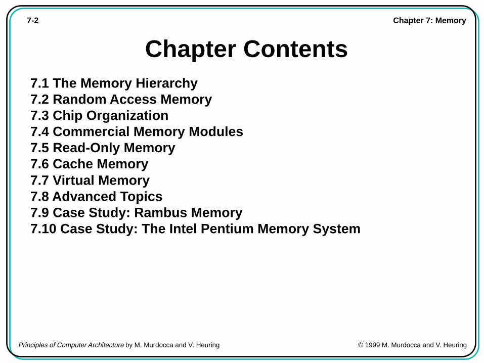
Chapter 7: Memory7-2
Principles of Computer Architecture by M. Murdocca and V. Heuring © 1999 M. Murdocca and V. Heuring
Chapter Contents7.1 The Memory Hierarchy7.2 Random Access Memory7.3 Chip Organization7.4 Commercial Memory Modules7.5 Read-Only Memory7.6 Cache Memory7.7 Virtual Memory7.8 Advanced Topics7.9 Case Study: Rambus Memory7.10 Case Study: The Intel Pentium Memory System
Chapter 7: Memory7-3
Principles of Computer Architecture by M. Murdocca and V. Heuring © 1999 M. Murdocca and V. Heuring
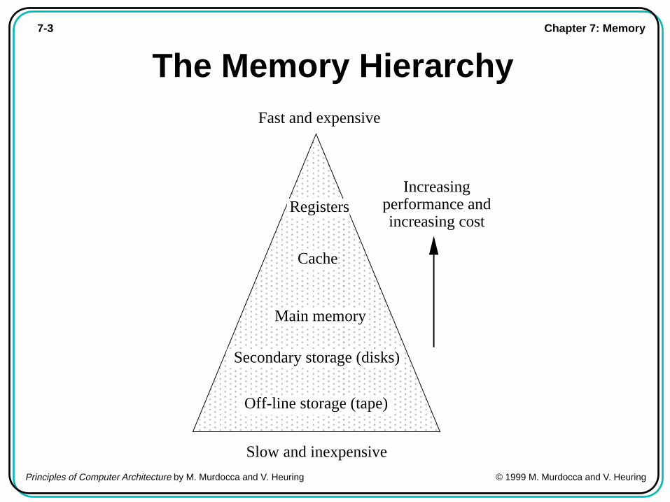
The Memory Hierarchy
Registers
Cache
Main memory
Secondary storage (disks)
Off-line storage (tape)
Fast and expensive
Slow and inexpensive
Increasing performance andincreasing cost
Chapter 7: Memory7-4
Principles of Computer Architecture by M. Murdocca and V. Heuring © 1999 M. Murdocca and V. Heuring
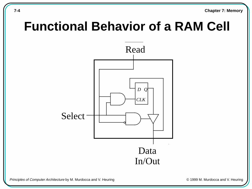
Functional Behavior of a RAM Cell
QD
CLK
Read
Select
Data In/Out
Chapter 7: Memory7-5
Principles of Computer Architecture by M. Murdocca and V. Heuring © 1999 M. Murdocca and V. Heuring
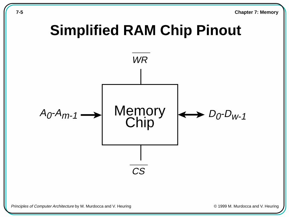
Simplified RAM Chip Pinout
A0-Am-1 D0-Dw-1
WR
CS
Memory Chip
Chapter 7: Memory7-6
Principles of Computer Architecture by M. Murdocca and V. Heuring © 1999 M. Murdocca and V. Heuring
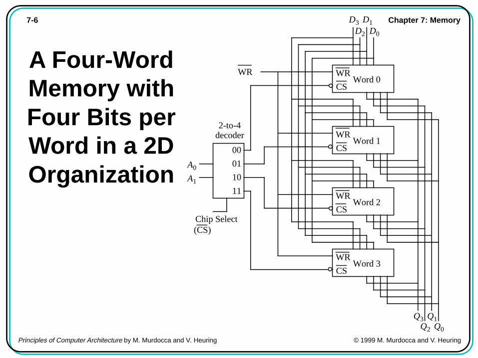
A Four-WordMemory withFour Bits perWord in a 2DOrganization
D3D2
D1D0
Q3Q2
Q1Q0
WR
CSWord 0
00
01
10
11
A0
A1
WR
WR
CSWord 1
WR
CSWord 2
WR
CSWord 3
2-to-4decoder
Chip Select(CS)
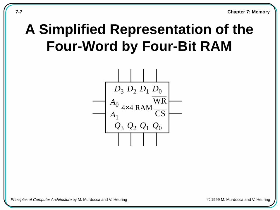
Chapter 7: Memory7-7
Principles of Computer Architecture by M. Murdocca and V. Heuring © 1999 M. Murdocca and V. Heuring
A Simplified Representation of theFour-Word by Four-Bit RAM
Q3 Q2 Q1 Q0
A0
A1
WR
CS
D3 D2 D1 D0
4× 4 RAM
Chapter 7: Memory7-8
Principles of Computer Architecture by M. Murdocca and V. Heuring © 1999 M. Murdocca and V. Heuring
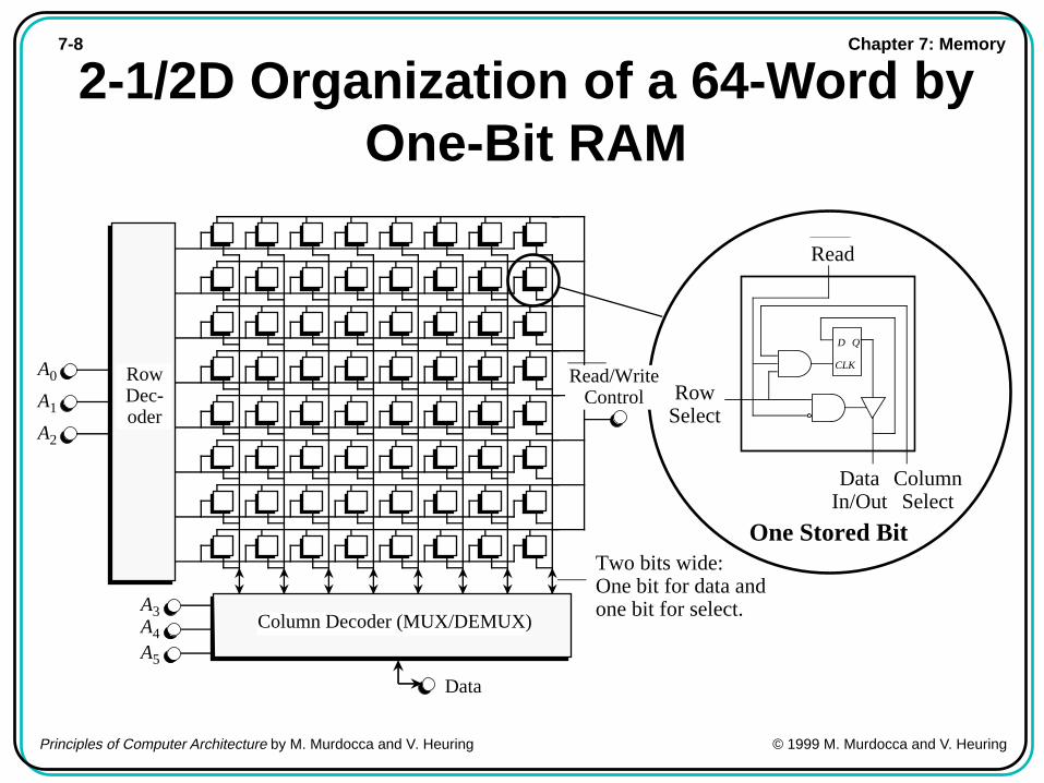
2-1/2D Organization of a 64-Word byOne-Bit RAM
RowDec-oder
Column Decoder (MUX/DEMUX)
A0
A1
A2
A3A4
A5
Data
One Stored Bit
QD
CLK
Read
Row Select
Column Select
Data In/Out
Read/WriteControl
Two bits wide:One bit for data andone bit for select.
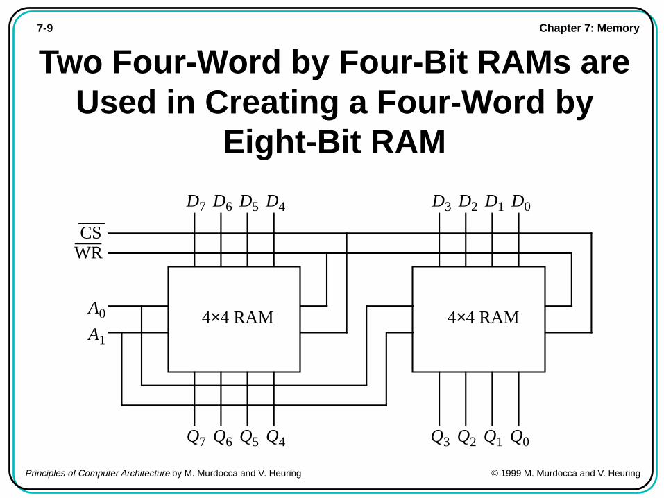
Chapter 7: Memory7-9
Principles of Computer Architecture by M. Murdocca and V. Heuring © 1999 M. Murdocca and V. Heuring
Two Four-Word by Four-Bit RAMs areUsed in Creating a Four-Word by
Eight-Bit RAM
A0
A1
WRCS
D7 D6 D5 D4 D3 D2 D1 D0
4× 4 RAM
Q7 Q6 Q5 Q4 Q3 Q2 Q1 Q0
4× 4 RAM
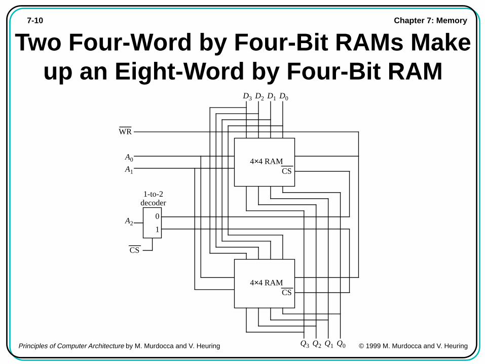
Chapter 7: Memory7-10
Principles of Computer Architecture by M. Murdocca and V. Heuring © 1999 M. Murdocca and V. Heuring
Two Four-Word by Four-Bit RAMs Makeup an Eight-Word by Four-Bit RAM
A0
A1
WR
D3 D2 D1 D0
4× 4 RAM
Q3 Q2 Q1 Q0
4× 4 RAM
1-to-2decoder
0
1A2
CS
CS
CS
Chapter 7: Memory7-11
Principles of Computer Architecture by M. Murdocca and V. Heuring © 1999 M. Murdocca and V. Heuring
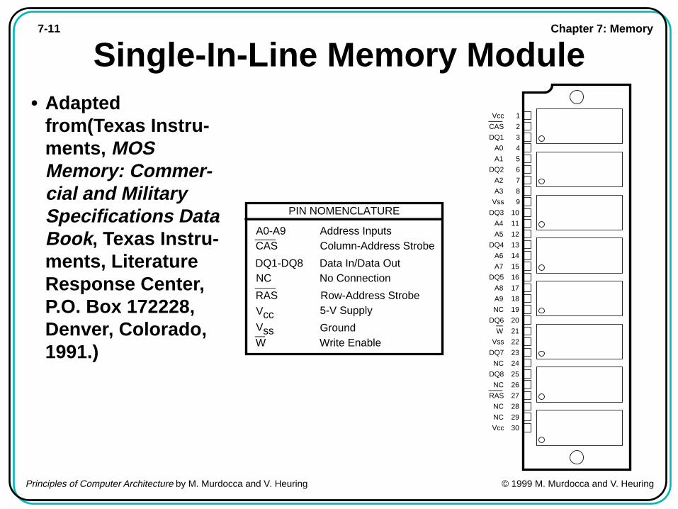
Single-In-Line Memory Module
1
2
3
4
5
6
7
8
9
10
11
12
13
14
15
16
17
18
19
20
21
22
23
24
25
26
27
28
29
30
Vcc
CAS
DQ1
A0
A1
DQ2
A2
A3
Vss
DQ3
A4
A5
DQ4
A6
A7
DQ5
A8
A9
NC
DQ6
W
Vss
DQ7
NC
DQ8
NC
RAS
NC
NC
Vcc
PIN NOMENCLATURE
Address InputsColumn-Address Strobe
Data In/Data OutNo Connection
Row-Address Strobe5-V Supply
GroundWrite Enable
DQ1-DQ8
CASA0-A9
NC
RASVccVssW
• Adaptedfrom(Texas Instru-ments, MOSMemory: Commer-cial and MilitarySpecifications DataBook , Texas Instru-ments, LiteratureResponse Center,P.O. Box 172228,Denver, Colorado,1991.)
Chapter 7: Memory7-12
Principles of Computer Architecture by M. Murdocca and V. Heuring © 1999 M. Murdocca and V. Heuring
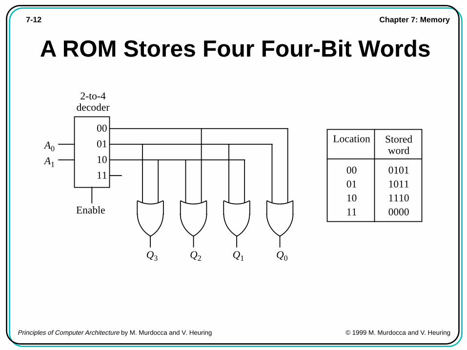
A ROM Stores Four Four-Bit Words
Q3 Q2 Q1 Q0
00
01
10
11
A0
A1
2-to-4decoder
Enable
Location Storedword
00011011
0101101111100000
Chapter 7: Memory7-13
Principles of Computer Architecture by M. Murdocca and V. Heuring © 1999 M. Murdocca and V. Heuring
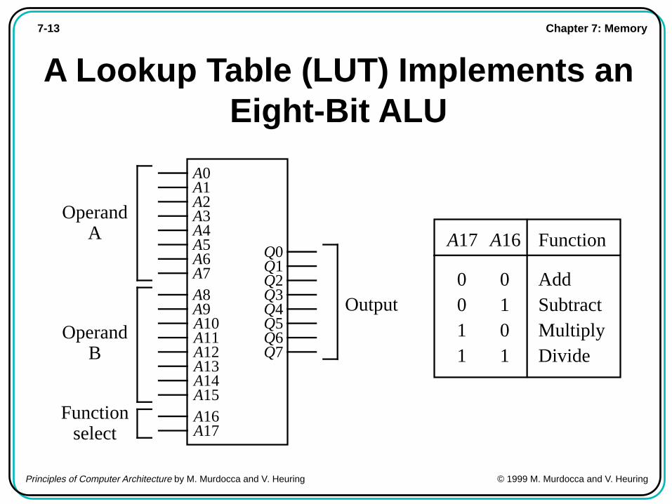
A Lookup Table (LUT) Implements anEight-Bit ALU
A0A1A2A3A4A5A6A7A8A9A10A11A12A13A14A15A16A17
Q0Q1Q2Q3Q4Q5Q6Q7
Operand A
Operand B
Functionselect
Output0011
0101
AddSubtractMultiplyDivide
A17 A16 Function
Chapter 7: Memory7-14
Principles of Computer Architecture by M. Murdocca and V. Heuring © 1999 M. Murdocca and V. Heuring
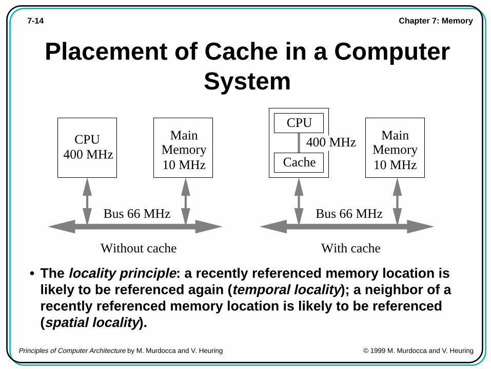
Placement of Cache in a ComputerSystem
CPU400 MHz
MainMemory10 MHz
Bus 66 MHz
MainMemory10 MHz
Bus 66 MHz
CPU
Cache
400 MHz
Without cache With cache
• The locality principle : a recently referenced memory location islikely to be referenced again ( temporal locality ); a neighbor of arecently referenced memory location is likely to be referenced(spatial locality ).
Chapter 7: Memory7-15
Principles of Computer Architecture by M. Murdocca and V. Heuring © 1999 M. Murdocca and V. Heuring
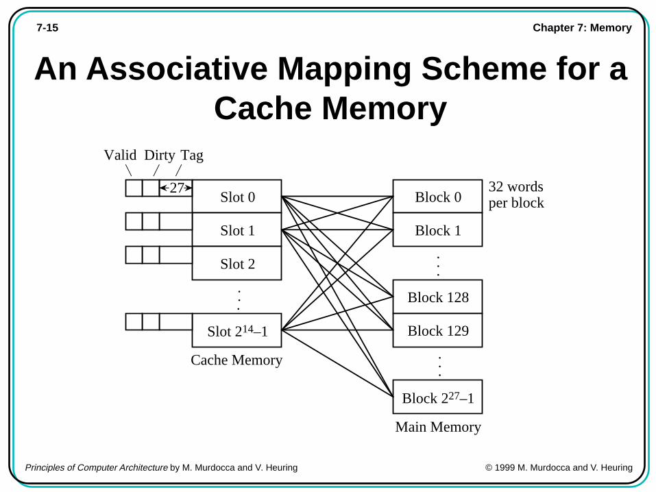
An Associative Mapping Scheme for aCache Memory
Slot 0
Slot 1
Slot 2
Slot 214–1
.
.
.
.
.
.
Block 0
Block 1
Block 128
Block 129
Block 227–1
Cache Memory
Main Memory
TagValid Dirty
32 words per block
27
.
.
.
Chapter 7: Memory7-16
Principles of Computer Architecture by M. Murdocca and V. Heuring © 1999 M. Murdocca and V. Heuring
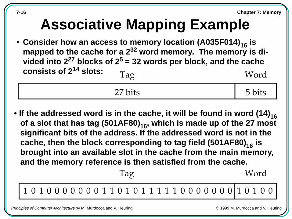
Associative Mapping Example• Consider how an access to memory location (A035F014) 16 is
mapped to the cache for a 2 32 word memory. The memory is di-vided into 2 27 blocks of 2 5 = 32 words per block, and the cacheconsists of 2 14 slots:
27 bits 5 bits
Tag Word
Tag Word
1 0 1 0 0 0 0 0 0 0 1 1 0 1 0 1 1 1 1 1 0 0 0 0 0 0 0 1 0 1 0 0
• If the addressed word is in the cache, it will be found in word (14) 16of a slot that has tag (501AF80) 16, which is made up of the 27 mostsignificant bits of the address. If the addressed word is not in thecache, then the block corresponding to tag field (501AF80) 16 isbrought into an available slot in the cache from the main memory,and the memory reference is then satisfied from the cache.
Chapter 7: Memory7-17
Principles of Computer Architecture by M. Murdocca and V. Heuring © 1999 M. Murdocca and V. Heuring
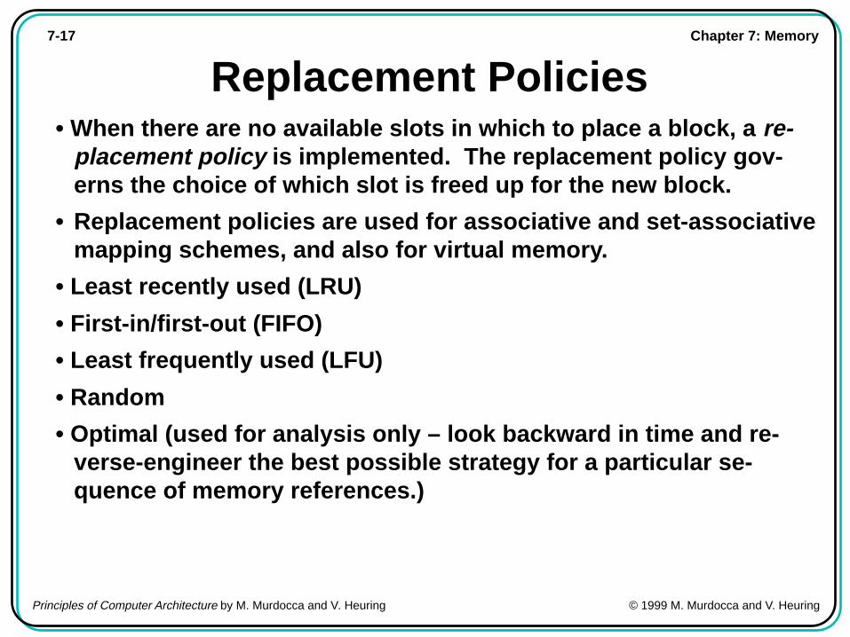
Replacement Policies• When there are no available slots in which to place a block, a re-
placement policy is implemented. The replacement policy gov-erns the choice of which slot is freed up for the new block.
• Replacement policies are used for associative and set-associativemapping schemes, and also for virtual memory.
• Least recently used (LRU)
• First-in/first-out (FIFO)
• Least frequently used (LFU)
• Random
• Optimal (used for analysis only – look backward in time and re-verse-engineer the best possible strategy for a particular se-quence of memory references.)
Chapter 7: Memory7-18
Principles of Computer Architecture by M. Murdocca and V. Heuring © 1999 M. Murdocca and V. Heuring
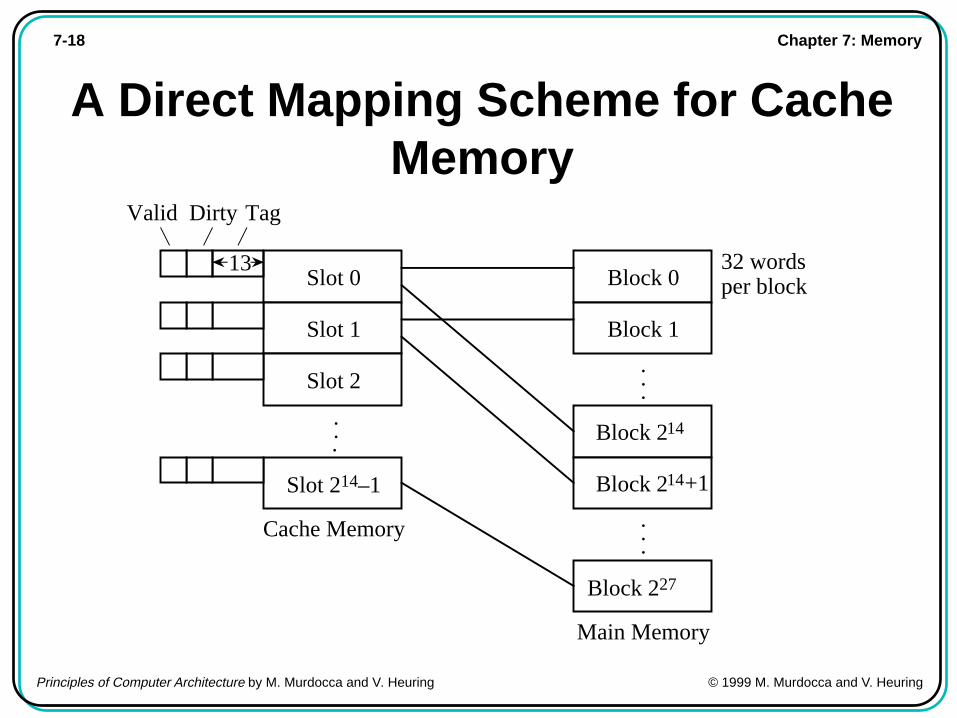
A Direct Mapping Scheme for CacheMemory
Slot 0
Slot 1
Slot 2
Slot 214–1
.
..
.
.
.
.
.
.
Block 0
Block 1
Block 2
Block 2
Block 227
+1
Cache Memory
Main Memory
TagValid Dirty
32 words per block
13
14
14
Chapter 7: Memory7-19
Principles of Computer Architecture by M. Murdocca and V. Heuring © 1999 M. Murdocca and V. Heuring
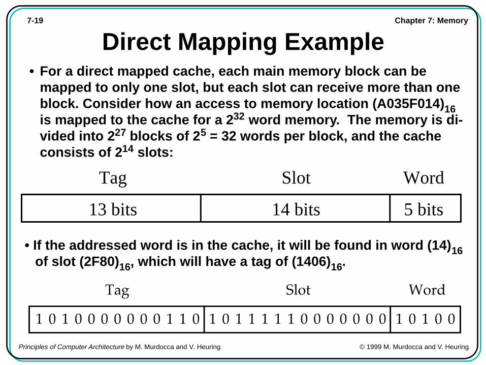
Direct Mapping Example• For a direct mapped cache, each main memory block can be
mapped to only one slot, but each slot can receive more than oneblock. Consider how an access to memory location (A035F014) 16is mapped to the cache for a 2 32 word memory. The memory is di-vided into 2 27 blocks of 2 5 = 32 words per block, and the cacheconsists of 2 14 slots:
• If the addressed word is in the cache, it will be found in word (14) 16of slot (2F80) 16, which will have a tag of (1406) 16.
13 bits 5 bits14 bits
Tag WordSlot
Tag Word
1 0 1 0 0 0 0 0 0 0 1 1 0 1 0 1 1 1 1 1 0 0 0 0 0 0 0 1 0 1 0 0
Slot
Chapter 7: Memory7-20
Principles of Computer Architecture by M. Murdocca and V. Heuring © 1999 M. Murdocca and V. Heuring
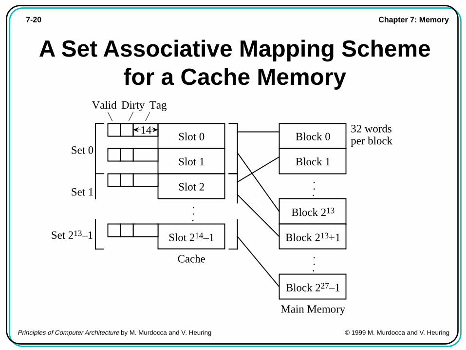
A Set Associative Mapping Schemefor a Cache Memory
Slot 0
Slot 1
Slot 2
Slot 214–1
.
.
.
.
.
.
.
.
.
Block 0
Block 1
Block 213
Block 213+1
Block 227–1
Cache
Main Memory
TagValid Dirty
32 words per block
Set 0
Set 1
Set 213–1
14
Chapter 7: Memory7-21
Principles of Computer Architecture by M. Murdocca and V. Heuring © 1999 M. Murdocca and V. Heuring
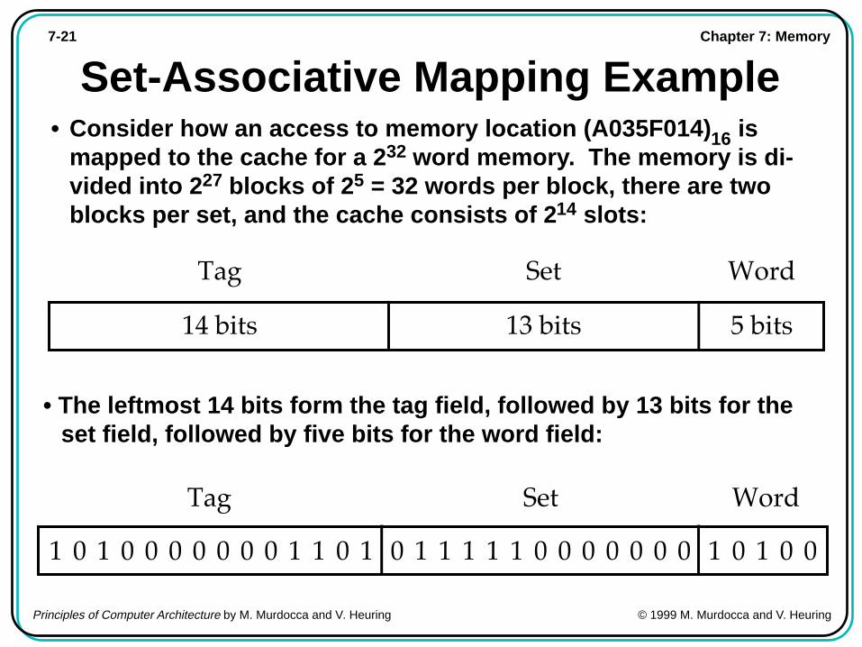
Set-Associative Mapping Example• Consider how an access to memory location (A035F014) 16 is
mapped to the cache for a 2 32 word memory. The memory is di-vided into 2 27 blocks of 2 5 = 32 words per block, there are twoblocks per set, and the cache consists of 2 14 slots:
• The leftmost 14 bits form the tag field, followed by 13 bits for theset field, followed by five bits for the word field:
Tag WordSet
14 bits 5 bits13 bits
Tag Word
1 0 1 0 0 0 0 0 0 0 1 1 0 1 0 1 1 1 1 1 0 0 0 0 0 0 0 1 0 1 0 0
Set
Chapter 7: Memory7-22
Principles of Computer Architecture by M. Murdocca and V. Heuring © 1999 M. Murdocca and V. Heuring
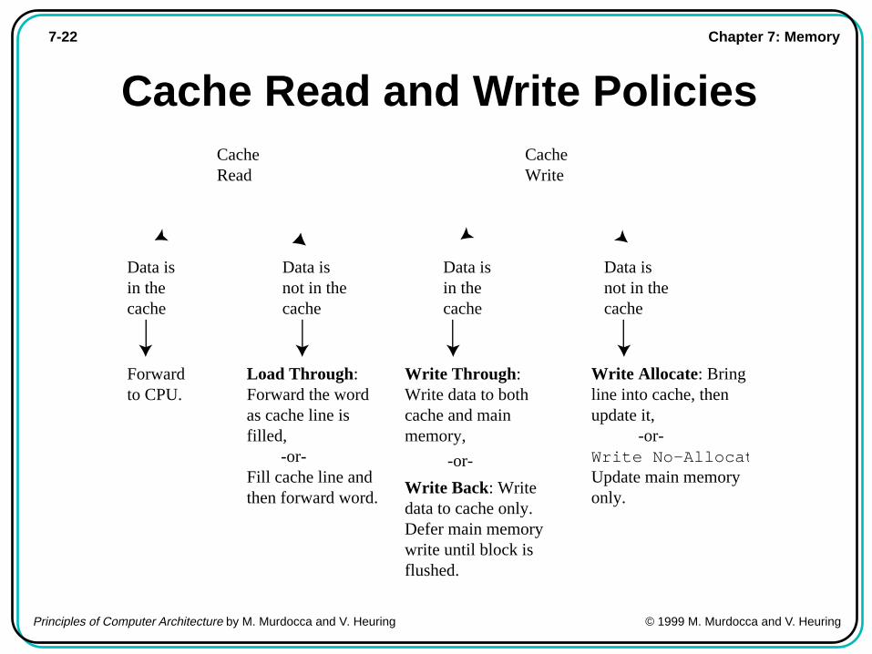
Cache Read and Write Policies Cache
Read Cache
Write
Data is in the cache
Data is not in the cache
Data is in the cache
Data is not in the cache
Forward to CPU.
Write Through: Write data to both cache and main memory,
Write Back: Write data to cache only. Defer main memory write until block is flushed.
Load Through: Forward the word as cache line is filled, -or- Fill cache line and then forward word.
Write Allocate: Bring line into cache, then update it, -or- Write No-AllocatUpdate main memory only.
-or-
Chapter 7: Memory7-23
Principles of Computer Architecture by M. Murdocca and V. Heuring © 1999 M. Murdocca and V. Heuring
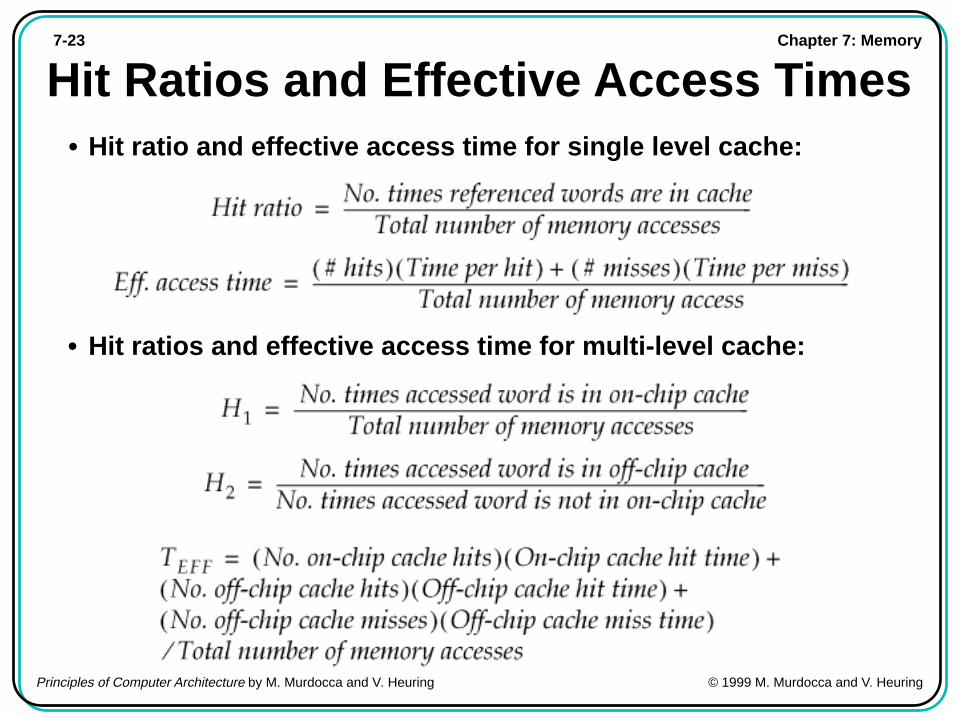
Hit Ratios and Effective Access Times• Hit ratio and effective access time for single level cache:
• Hit ratios and effective access time for multi-level cache:
Chapter 7: Memory7-24
Principles of Computer Architecture by M. Murdocca and V. Heuring © 1999 M. Murdocca and V. Heuring
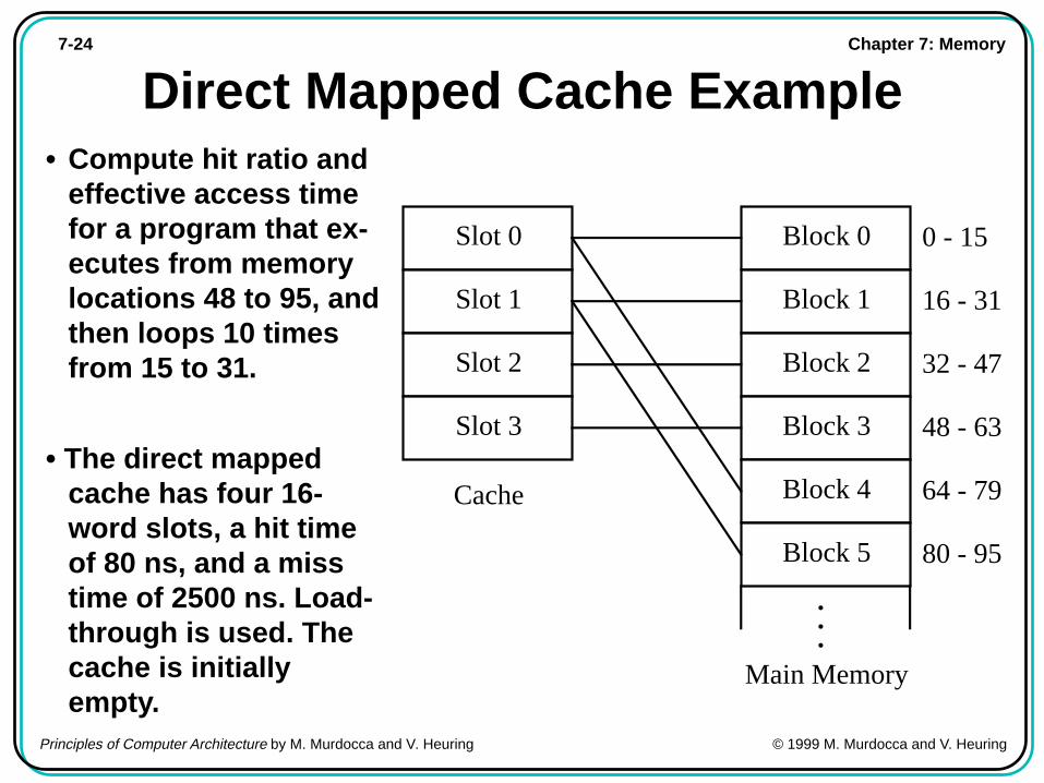
Direct Mapped Cache Example
Slot 0
Slot 1
Slot 2
Slot 3
Block 0
Block 1
Block 2
Block 3
Block 4
Block 5
0 - 15
Cache
Main Memory
16 - 31
32 - 47
48 - 63
64 - 79
80 - 95
.
.
.
• Compute hit ratio andeffective access timefor a program that ex-ecutes from memorylocations 48 to 95, andthen loops 10 timesfrom 15 to 31.
• The direct mappedcache has four 16-word slots, a hit timeof 80 ns, and a misstime of 2500 ns. Load-through is used. Thecache is initiallyempty.
Chapter 7: Memory7-25
Principles of Computer Architecture by M. Murdocca and V. Heuring © 1999 M. Murdocca and V. Heuring
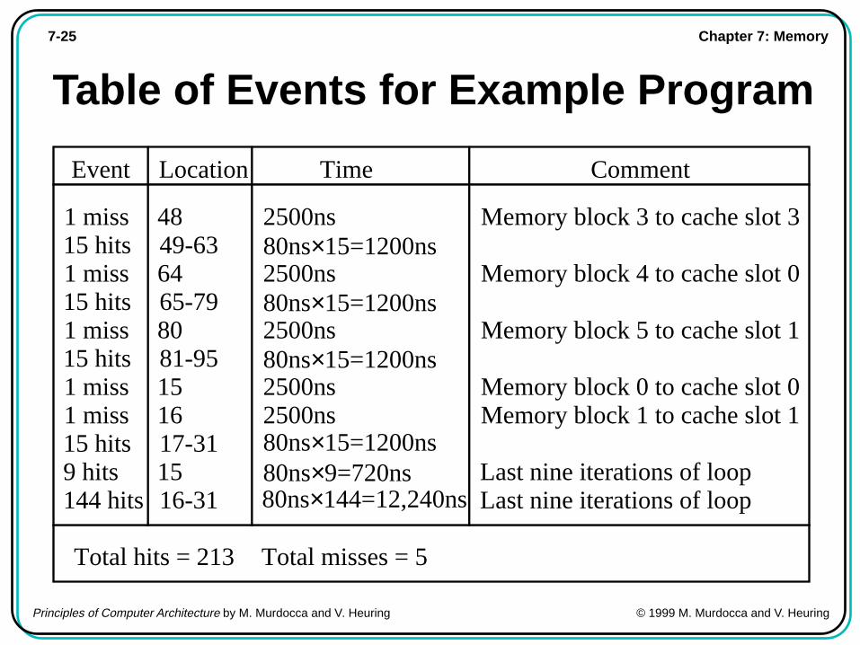
Table of Events for Example Program
Event Location Time Comment
48 2500ns Memory block 3 to cache slot 31 miss49-63 80ns× 15=1200ns15 hits64 2500ns Memory block 4 to cache slot 01 miss65-79 80ns× 15=1200ns15 hits80 2500ns Memory block 5 to cache slot 11 miss81-95 80ns× 15=1200ns15 hits15 2500ns Memory block 0 to cache slot 01 miss16 2500ns Memory block 1 to cache slot 11 miss17-31 80ns× 15=1200ns15 hits15 80ns× 9=720ns Last nine iterations of loop9 hits16-31 80ns× 144=12,240ns Last nine iterations of loop144 hits
Total hits = 213 Total misses = 5
Chapter 7: Memory7-26
Principles of Computer Architecture by M. Murdocca and V. Heuring © 1999 M. Murdocca and V. Heuring
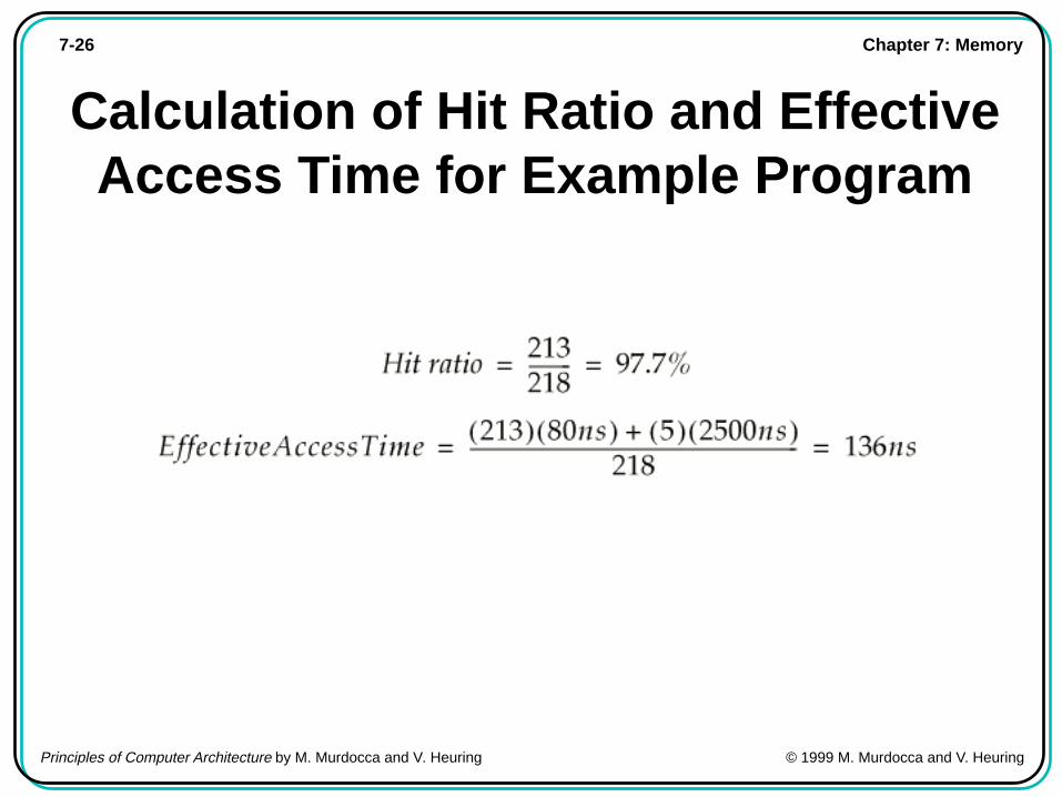
Calculation of Hit Ratio and EffectiveAccess Time for Example Program
Chapter 7: Memory7-27
Principles of Computer Architecture by M. Murdocca and V. Heuring © 1999 M. Murdocca and V. Heuring
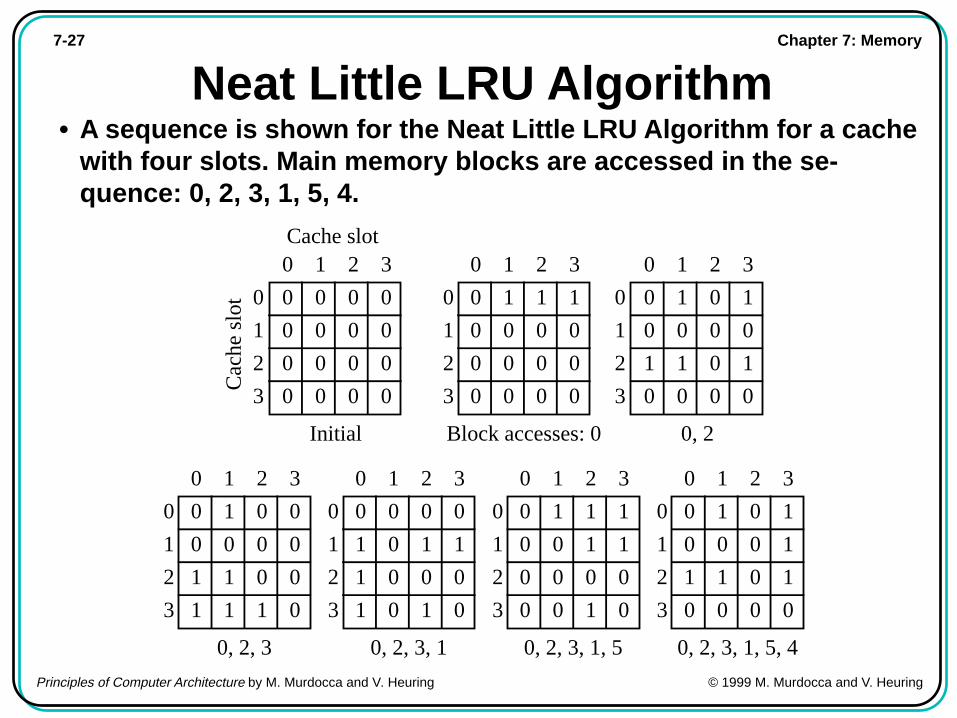
Neat Little LRU Algorithm• A sequence is shown for the Neat Little LRU Algorithm for a cache
with four slots. Main memory blocks are accessed in the se-quence: 0, 2, 3, 1, 5, 4.
0
1
2
3
0 1 2 3
0 0 0 0
0 0 0 0
0 0 0 0
0 0 0 0
Cache slotC
ache
slo
t
0
1
2
3
0 1 2 3
0 1 0 0
0 0 0 0
1 1 0 0
1 1 1 0
0
1
2
3
0 1 2 3
0 0 0 0
1 0 1 1
1 0 0 0
1 0 1 0
0
1
2
3
0 1 2 3
0 1 1 1
0 0 1 1
0 0 0 0
0 0 1 0
0
1
2
3
0 1 2 3
0 1 0 1
0 0 0 1
1 1 0 1
0 0 0 0
0
1
2
3
0 1 2 3
0 1 1 1
0 0 0 0
0 0 0 0
0 0 0 0
0
1
2
3
0 1 2 3
0 1 0 1
0 0 0 0
1 1 0 1
0 0 0 0
Initial Block accesses: 0 0, 2
0, 2, 3 0, 2, 3, 1 0, 2, 3, 1, 5 0, 2, 3, 1, 5, 4
Chapter 7: Memory7-28
Principles of Computer Architecture by M. Murdocca and V. Heuring © 1999 M. Murdocca and V. Heuring
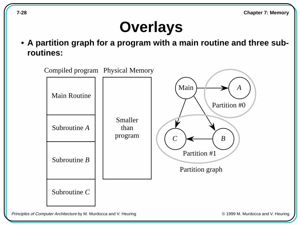
Overlays• A partition graph for a program with a main routine and three sub-
routines:
Main Routine
Subroutine A
Subroutine B
Subroutine C
Compiled program
Main A
BC
Partition graph
Partition #0
Partition #1
Physical Memory
Smaller than
program
Chapter 7: Memory7-29
Principles of Computer Architecture by M. Murdocca and V. Heuring © 1999 M. Murdocca and V. Heuring
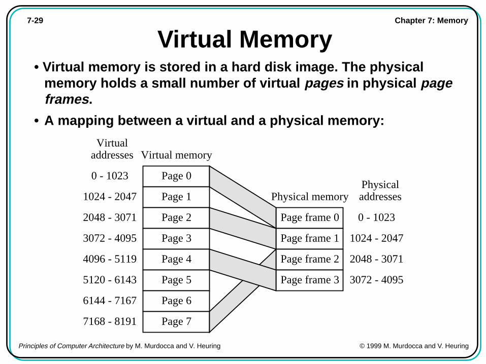
Virtual Memory• Virtual memory is stored in a hard disk image. The physical
memory holds a small number of virtual pages in physical pageframes .
• A mapping between a virtual and a physical memory:
Virtual memory
Physical memory
Page frame 0
Page frame 1
Page frame 2
Page frame 3
Page 0
Page 1
Page 2
Page 3
Page 4
Page 5
Page 6
Page 7
Virtual addresses
Physical addresses
0 - 1023
1024 - 2047
2048 - 3071
3072 - 4095
4096 - 5119
5120 - 6143
6144 - 7167
7168 - 8191
0 - 1023
1024 - 2047
2048 - 3071
3072 - 4095
Chapter 7: Memory7-30
Principles of Computer Architecture by M. Murdocca and V. Heuring © 1999 M. Murdocca and V. Heuring
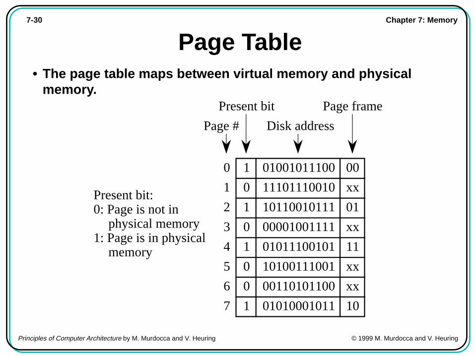
Page Table• The page table maps between virtual memory and physical
memory.
Present bit:0: Page is not in physical memory1: Page is in physical memory
Present bit
Page #
0
1
2
3
4
5
6
7
1
0
1
0
1
0
0
1
00
xx
01
xx
11
xx
xx
10
Disk address
Page frame
01001011100
11101110010
10110010111
00001001111
01011100101
10100111001
00110101100
01010001011
Chapter 7: Memory7-31
Principles of Computer Architecture by M. Murdocca and V. Heuring © 1999 M. Murdocca and V. Heuring
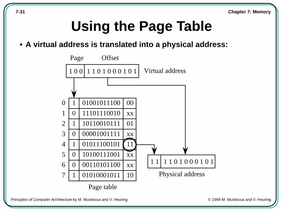
Using the Page Table• A virtual address is translated into a physical address:
0
1
2
3
4
5
6
7
1
0
1
0
1
0
0
1
00
xx
01
xx
11
xx
xx
10
01001011100
11101110010
10110010111
00001001111
01011100101
10100111001
00110101100
01010001011
1 0 0 1 1 0 1 0 0 0 1 0 1 Virtual address
Page table
1 1 1 1 0 1 0 0 0 1 0 1
Physical address
Page Offset
Chapter 7: Memory7-32
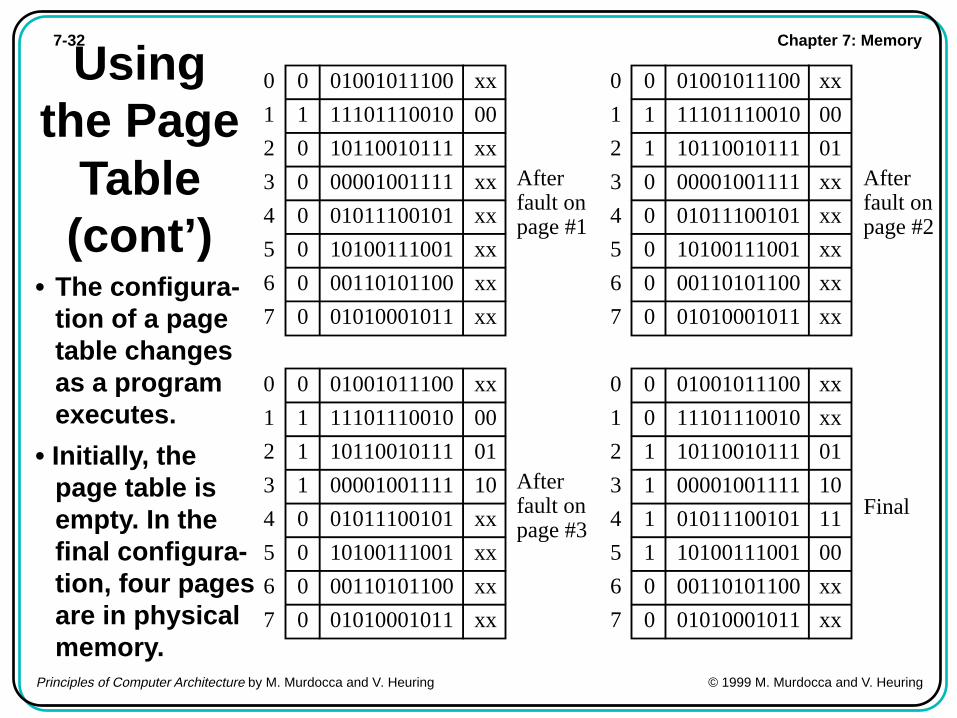
Principles of Computer Architecture by M. Murdocca and V. Heuring © 1999 M. Murdocca and V. Heuring
Usingthe Page
Table(cont’)
• The configura-tion of a pagetable changesas a programexecutes.
• Initially, thepage table isempty. In thefinal configura-tion, four pagesare in physicalmemory.
0
1
2
3
4
5
6
7
0
1
0
0
0
0
0
0
xx
00
xx
xx
xx
xx
xx
xx
01001011100
11101110010
10110010111
00001001111
01011100101
10100111001
00110101100
01010001011
After fault on page #1
0
1
2
3
4
5
6
7
0
1
1
1
0
0
0
0
xx
00
01
10
xx
xx
xx
xx
01001011100
11101110010
10110010111
00001001111
01011100101
10100111001
00110101100
01010001011
0
1
2
3
4
5
6
7
0
1
1
0
0
0
0
0
xx
00
01
xx
xx
xx
xx
xx
01001011100
11101110010
10110010111
00001001111
01011100101
10100111001
00110101100
01010001011
0
1
2
3
4
5
6
7
0
0
1
1
1
1
0
0
xx
xx
01
10
11
00
xx
xx
01001011100
11101110010
10110010111
00001001111
01011100101
10100111001
00110101100
01010001011
Final
After fault on page #2
After fault on page #3
Chapter 7: Memory7-33
Principles of Computer Architecture by M. Murdocca and V. Heuring © 1999 M. Murdocca and V. Heuring
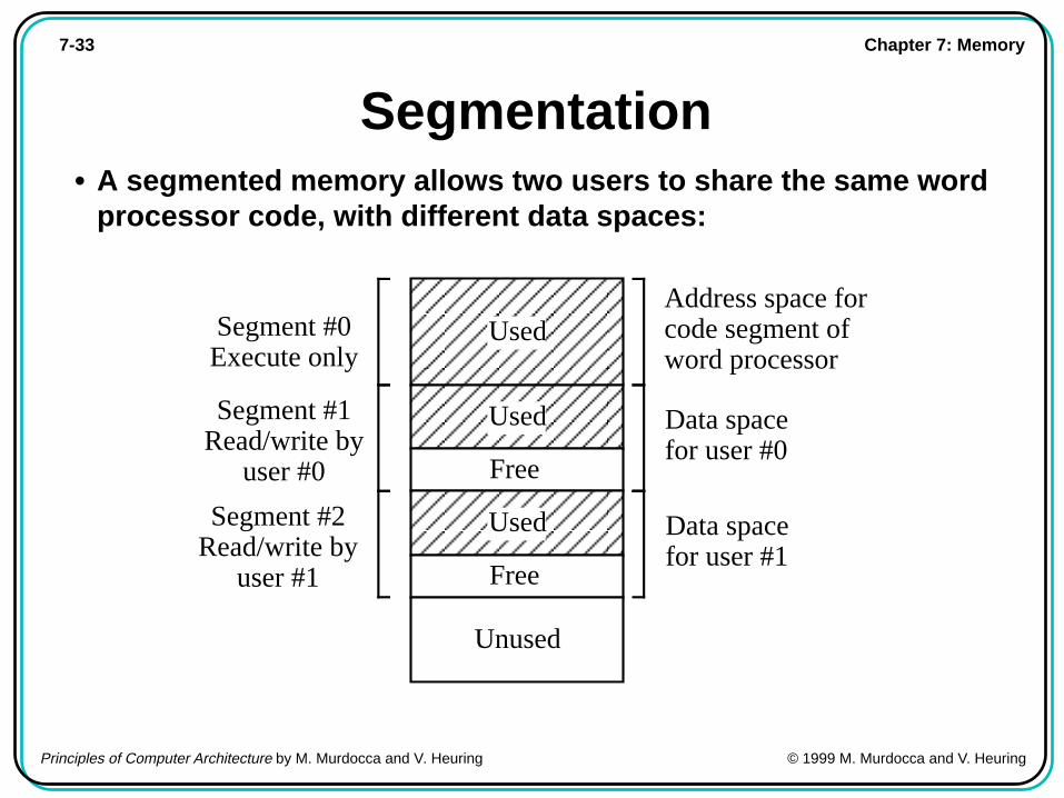
Segmentation• A segmented memory allows two users to share the same word
processor code, with different data spaces:
Address space for code segment of word processor
Data space for user #0
Data space for user #1
Used
Used
Used
Free
Free
Unused
Segment #0Execute only
Segment #1Read/write by
user #0
Segment #2 Read/write by
user #1
Chapter 7: Memory7-34
Principles of Computer Architecture by M. Murdocca and V. Heuring © 1999 M. Murdocca and V. Heuring
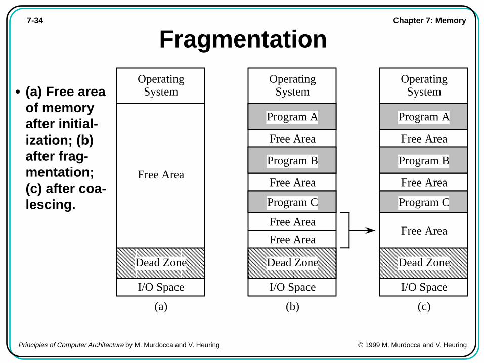
Fragmentation
• (a) Free areaof memoryafter initial-ization; (b)after frag-mentation;(c) after coa-lescing.
(a) (b) (c)
Operating System
Free Area
I/O Space
Dead Zone
Operating System
I/O Space
Dead Zone
Free Area
Free Area
Free Area
Free Area
Program A
Program B
Program C
Operating System
I/O Space
Dead Zone
Free Area
Free Area
Free Area
Program A
Program B
Program C
Chapter 7: Memory7-35
Principles of Computer Architecture by M. Murdocca and V. Heuring © 1999 M. Murdocca and V. Heuring
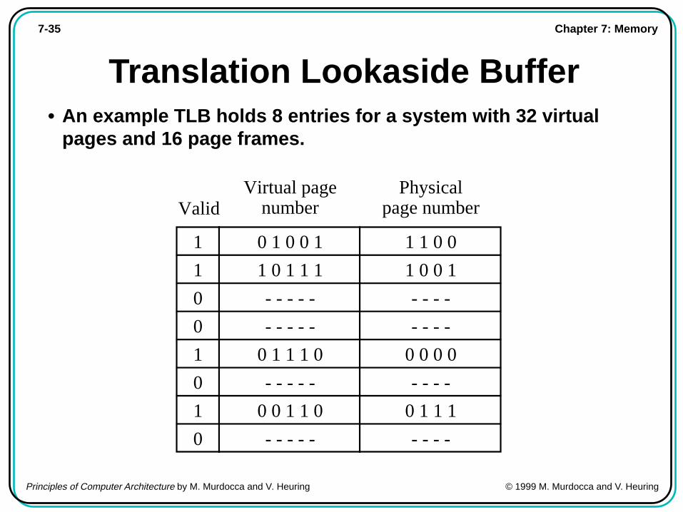
Translation Lookaside Buffer• An example TLB holds 8 entries for a system with 32 virtual
pages and 16 page frames.
ValidVirtual page
numberPhysical
page number
1
1
0
0
1
0
1
0
0 1 0 0 1 1 1 0 0
1 0 1 1 1 1 0 0 1
- - - - - - - - -
- - - - - - - - -
0 1 1 1 0 0 0 0 0
- - - - - - - - -
0 0 1 1 0 0 1 1 1
- - - - - - - - -
Chapter 7: Memory7-36
Principles of Computer Architecture by M. Murdocca and V. Heuring © 1999 M. Murdocca and V. Heuring
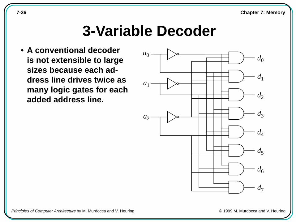
3-Variable Decoder• A conventional decoder
is not extensible to largesizes because each ad-dress line drives twice asmany logic gates for eachadded address line.
d0
d1
d2
d3
d4
d5
d6
d7
a0
a1
a2
Chapter 7: Memory7-37
Principles of Computer Architecture by M. Murdocca and V. Heuring © 1999 M. Murdocca and V. Heuring
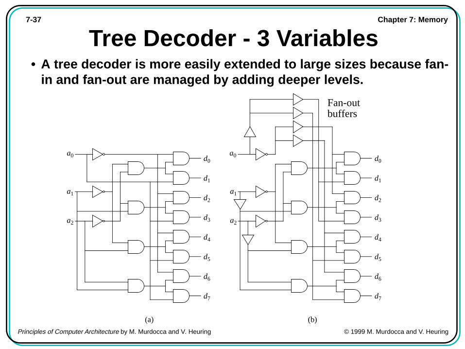
Tree Decoder - 3 Variables• A tree decoder is more easily extended to large sizes because fan-
in and fan-out are managed by adding deeper levels.
a0
a1
d0
d1
d2
d3
d4
d5
d6
d7
a2
(a)
a0
a1
d0
d1
d2
d3
d4
d5
d6
d7
a2
(b)
Fan-out buffers
Chapter 7: Memory7-38
Principles of Computer Architecture by M. Murdocca and V. Heuring © 1999 M. Murdocca and V. Heuring
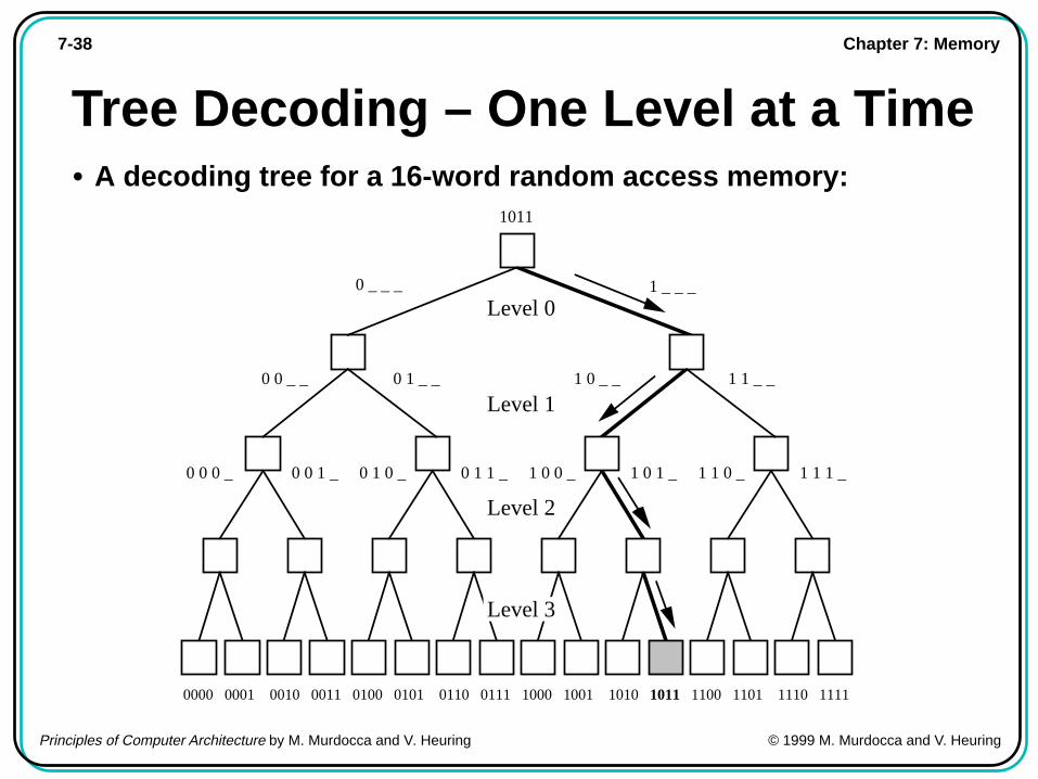
Tree Decoding – One Level at a Time• A decoding tree for a 16-word random access memory:
0000 0001 0010 0011 0100 0101 0110 0111 1000 1001 1010 1011 1100 1101 1110 1111
1011
0 _ _ _ 1 _ _ _
0 0 _ _ 0 1 _ _ 1 0 _ _ 1 1 _ _
0 0 0 _ 0 0 1 _ 0 1 0 _ 0 1 1 _ 1 0 0 _ 1 0 1 _ 1 1 0 _ 1 1 1 _
Level 0
Level 1
Level 2
Level 3

Chapter 7: Memory7-39
Principles of Computer Architecture by M. Murdocca and V. Heuring © 1999 M. Murdocca and V. Heuring
Content Addressable Memory –Addressing
• Relationships between random access memory and content ad-dressable memory:
Address Value Field1 Field2 Field3
Random access memory Content addressable memory
0000A000 0F0F0000 000 A 9E186734F10F000000FE6810223152467CC345091700392B1110034561
0000A0040000A0080000A00C0000A0100000A0140000A0180000A01C
011149091000749000575
074EC01
F00100FE6E5084
32 bits 32 bits 12 bits 4 bits 8 bits
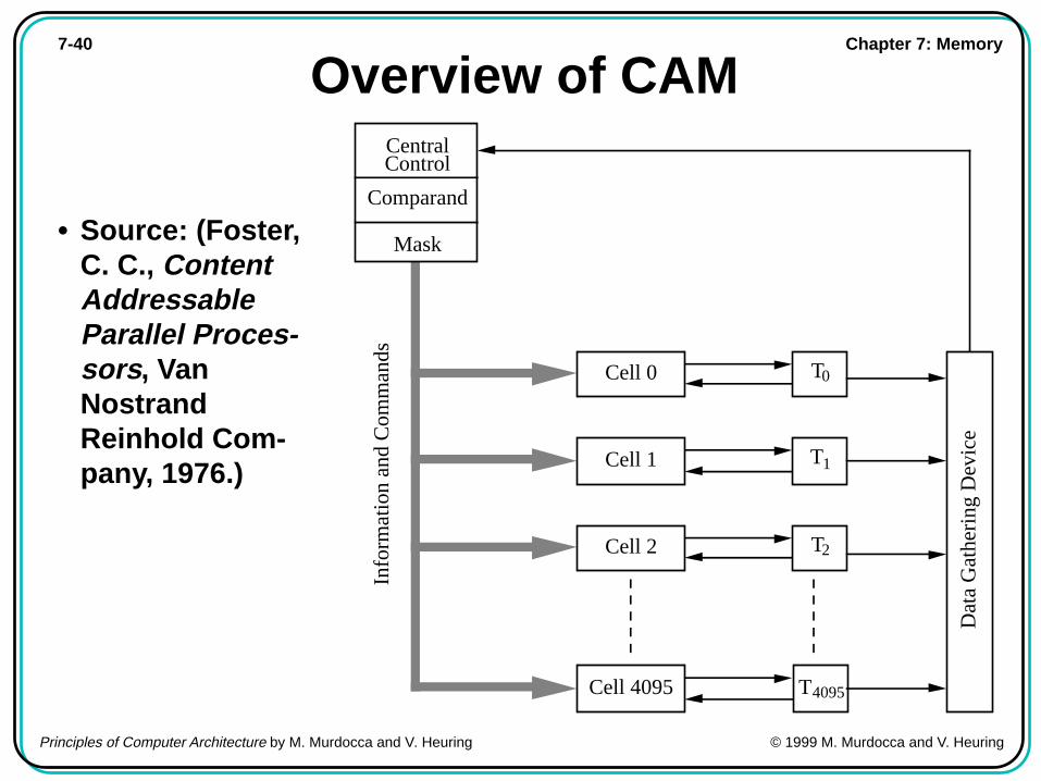
Chapter 7: Memory7-40
Principles of Computer Architecture by M. Murdocca and V. Heuring © 1999 M. Murdocca and V. Heuring
Overview of CAM
• Source: (Foster,C. C., ContentAddressableParallel Proces-sors , VanNostrandReinhold Com-pany, 1976.)
Info
rmat
ion
and
Com
man
ds
Dat
a G
athe
ring
Dev
ice
T0
T1
T2
T4095
Cell 0
Cell 1
Cell 2
Cell 4095
CentralControl
Comparand
Mask
Chapter 7: Memory7-41
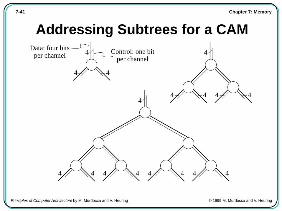
Principles of Computer Architecture by M. Murdocca and V. Heuring © 1999 M. Murdocca and V. Heuring
Addressing Subtrees for a CAM4
44 44
44 44 44 44
4
4
4
4
Control: one bitper channel
Data: four bitsper channel
Chapter 7: Memory7-42
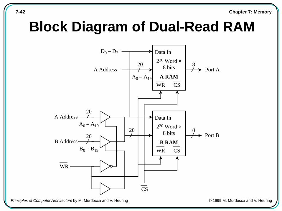
Principles of Computer Architecture by M. Murdocca and V. Heuring © 1999 M. Murdocca and V. Heuring
Block Diagram of Dual-Read RAM
Data In
220 Word × 8 bits
A RAM
WR CS
D0 – D7
A0 – A19
20A Address
8Port A
Data In
220 Word × 8 bits
B RAM
WR CS
8Port B
A0 – A19
20A Address
B0 – B19
20B Address
20
WR
CS
Chapter 7: Memory7-43
Principles of Computer Architecture by M. Murdocca and V. Heuring © 1999 M. Murdocca and V. Heuring
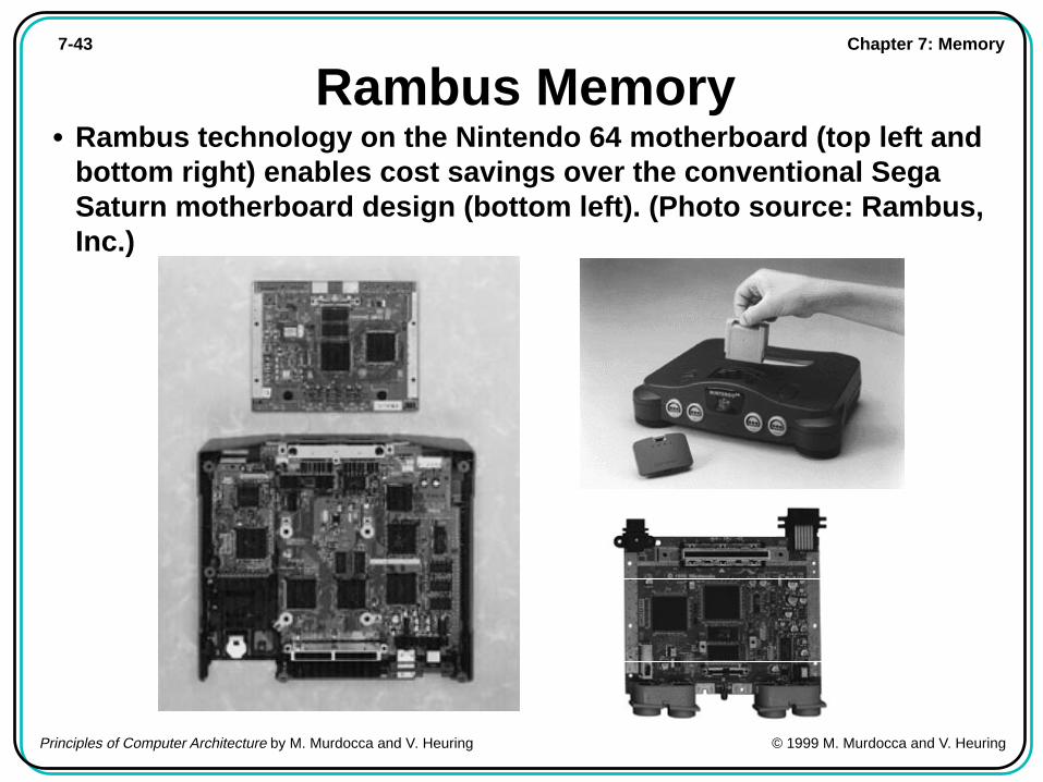
Rambus Memory• Rambus technology on the Nintendo 64 motherboard (top left and
bottom right) enables cost savings over the conventional SegaSaturn motherboard design (bottom left). (Photo source: Rambus,Inc.)
Chapter 7: Memory7-44
Principles of Computer Architecture by M. Murdocca and V. Heuring © 1999 M. Murdocca and V. Heuring
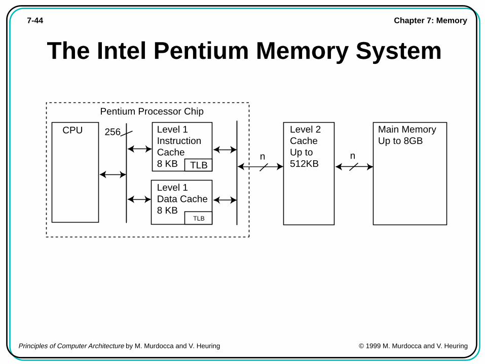
The Intel Pentium Memory System
CPU Level 1 Instruction Cache 8 KB
Level 1 Data Cache 8 KB
Level 2 Cache Up to 512KB
Main Memory Up to 8GB
256
Pentium Processor Chip
n nTLB
TLB


![COMPUTER ORGANIZATION Subject Code: 10CS46 - VTU Solutionvtusolution.in/.../cse-iii-computer__organization_[15cs34]-notes.pdf · COMPUTER ORGANIZATION 10CS46 . COMPUTER ORGANIZATION](https://img.pdfslide.net/doc/110x75/5b7970717f8b9a331e8dcaf3/computer-organization-subject-code-10cs46-vtu-15cs34-notespdf-computer.jpg)