Embed Size (px)
Citation preview
Concept Analysis for High-Voltage Direct-Current
Circuit Breakers for Application in a Network of
HVDC Transmission
Von der Fakultät für Maschinenbau, Elektrotechnik und Wirtschaftsingenieurwesen
der Brandenburgischen Technischen Universität Cottbus - Senftenberg zur Erlangung des
akademischen Grades eines Doktor-Ingenieurs
genehmigte Dissertation
vorgelegt von
Master of Science
Maxim Bonkarev
Geboren am 6. Juli 1987 in Nowosybkow, Russland
Vorsitzender: Prof. Dr.-Ing. Harald Fien
Gutachter: Prof. Dr.-Ing. Dr. Heinz-Helmut Schramm
Gutachter: Prof. Dr.-Ing. Harald Schwarz
Tag der mündlichen Prüfung: 14. April 2015

I
ACKNOWLEDGMENT
I wish to express my gratitude to Prof. Dr.-Ing. Dr. Heinz-Helmut Schramm for his direct
supervision of my work and whose contribution is difficult to overvalue. I highly appreciate
the efforts of Prof. Dr.-Ing. Harald Schwarz, Dr. Harald Fien and Dr. Norbert Trapp in
organising the International Graduate School, as a part of which this thesis is written. I also
express my special thanks to Mr. Lutz-Rüdiger Jänicke for his cooperation. The financial
support of this research project provided by Siemens AG Berlin is gratefully acknowledged,
too.
Maxim Bonkarev
2014

II
ABSTRACT
For several decades HVDC technology was used primarily for point-to-point bulk power
transmission. Although multiterminal HVDC systems are very few in number, it is expected
that multiple HVDC links may be interconnected into HVDC transmission grid. Since every
meshed grid requires reliable protection solution, an HVDC circuit breaker must be developed
and introduced. This thesis focuses on the performance evaluation of different HVDC circuit
breaker concepts. The performance evaluation study is carried out by means of numerical
simulations. The obtained quantitative results describe capabilities and limitations of different
HVDC circuit breaker concepts as well as the reaction of HVDC network on switching
operations. Different converter protection measures and in particular application of fault
current limiter were considered, too. Based on the research findings, a number of
recommendations for HVDC circuit breaker development are given and suggestions for
further research activities are presented.
KEYWORDS
Multi-terminal HVDC
HVDC circuit breaker
Fault protection methods
Network response
Simulation-based performance evaluation
III
ZUSAMMENFASSUNG
Seit mehreren Jahrzehnten wurde die HGÜ-Technologie hauptsächlich für die Punkt-zu-Punkt
Übertragung der großen Strommengen verwendet. Obwohl multiterminale HGÜ-Systeme
nicht zahlreich vertreten sind, wird erwartet, dass mehrere HGÜ-Leitungen in HGÜ-Netz
verbunden werden können. Da jedes vermaschte Stromnetz zuverlässige Schutzlösung
erfordert, muss ein HGÜ-Leistungsschalter entwickelt und eingesetzt werden. Diese
Doktorarbeit konzentriert sich auf die Leistungsbewertung der verschiedenen HGÜ-
Leistungsschalterkonzepte. Die Leistungsbewertungsstudie wird durch numerische
Simulationen durchgeführt. Die erhaltenen quantitativen Ergebnisse beschreiben
Möglichkeiten und Grenzen der verschiedenen HGÜ-Leistungsschalterkonzepte sowie die
Gegenwirkung des HGÜ-Netzwerkes auf Schaltvorgänge. Verschiedene
Umrichterschutzmaßnahmen und insbesondere Anwendung der Strombegrenzer wurden auch
untersucht. Auf Grundlage der Forschungsergebnisse werden eine Reihe von Empfehlungen
für die Entwicklung des HGÜ-Leistungsschalters gegeben und Anregungen für weitere
Forschungsaktivitäten vorgestellt.
SCHLAGWORTE
Multiterminale HGÜ
HGÜ-Leistungsschalter
Fehlerschutzmethoden
Netzwerkreaktion
Simulationsbasierte Leistungsbewertung

IV
TABLE OF CONTENTS
ACKNOWLEDGMENT……………………………………………………………………………………….….. I
ABSTRACT……………………………………………………………………………………………….………..I I
ZUSAMMENFASSUNG………………………………………………………………………………………….I II
LIST OF ABBREVIATIONS ............................................................................................................................... 1
LIST OF SYMBOLS ............................................................................................................................................. 2
1 INTRODUCTION .............................................................................................................................................. 4
1.1 GENERAL ASPECTS ......................................................................................................................................... 6
1.2 LITERATURE REVIEW ..................................................................................................................................... 8
1.3 RESEARCH GOALS ........................................................................................................................................ 13
1.4 THESIS OVERVIEW ........................................................................................................................................ 14
2 METHODS OF DIRECT CURRENT INTERRUPTION .......... .................................................................. 15
2.1 REQUIREMENTS TO HVDC BREAKERS ......................................................................................................... 15 2.2 EXISTING HVDC-BREAKER CONCEPTS ........................................................................................................ 16
2.2.1 Mechanical-based breakers ................................................................................................................. 17
2.2.1.1 Passive-type resonance breaker .............................................................................................................................18 2.2.1.2 Active-type resonance breaker ..............................................................................................................................22 2.2.1.3 Forced oscillations in DC breaking .......................................................................................................................25 2.2.1.4 Parametric oscillations in DC breaking .................................................................................................................27
2.2.2 Circuit breaker incorporating semiconductor devices ........................................................................ 30
2.2.2.1 Solid-state HVDC circuit breakers ........................................................................................................................32 2.2.2.2 Hybrid circuit breakers ...........................................................................................................................................36
3 MODELLING ................................................................................................................................................... 39
3.1 MODELLING OF SF6 MECHANICAL SWITCH .................................................................................................. 39
3.1.1 Physical fundamentals of the electric arc ............................................................................................ 40
3.1.2 Arc extinction theory ............................................................................................................................ 45
3.1.3 Arc-models overview............................................................................................................................ 47
3.1.3.1 Physical models ......................................................................................................................................................47 3.1.3.2 “Black-box” models ...............................................................................................................................................49
3.1.4 SF6-breaker model development ......................................................................................................... 51
3.1.5 Parameter determination and validation of the model ........................................................................ 54
3.2 VACUUM BREAKER MODELLING ................................................................................................................... 56 3.3 MODELLING OF SEMICONDUCTOR SWITCHES ............................................................................................... 59
4 PERFORMANCE STUDY OF THE HVDC CIRCUIT BREAKER CON CEPTS .................................... 60
4.1 EXISTING CONCEPTS EVALUATION ............................................................................................................... 60 4.1.1 Passive resonance circuit breaker ....................................................................................................... 61
4.1.2 Active resonance circuit breaker ......................................................................................................... 67
4.1.3 Forced oscillation DC circuit breaker ................................................................................................. 69
4.1.4 Semiconductor-based HVDC CB ......................................................................................................... 71
4.2 THE SELECTION CRITERIA FOR SEMICONDUCTOR SWITCHES ......................................................................... 74 4.3 TRANSIENT RECOVERY VOLTAGE (TRV) ..................................................................................................... 76
4.3.1 TRV for oscillation circuit breakers .................................................................................................... 77
4.3.2 TRV for semiconductor-based circuit breakers ................................................................................... 82
4.3.3 Recovery voltage grading and TRV peak shaving ............................................................................... 85

V
4.4 COMBINATION OF VACUUM AND SF6 SWITCHING TECHNIQUES .................................................................... 89 4.5 ANALYSIS OF TECHNICAL PERFORMANCE .................................................................................................... 93
5 PROTECTION SOLUTIONS FOR HVDC NETWORK ............................................................................. 97
5.1 INTERACTION OF CIRCUIT BREAKER AND DC VOLTAGE CONTROL SYSTEM .................................................. 97
5.2 PROTECTIVE MEASURES FROM THE SYSTEM POINT OF VIEW ....................................................................... 101 5.3 INTERACTION BETWEEN FAULT CURRENT LIMITER AND A CONVERTOR ...................................................... 104
6 CONCLUSIONS AND RECOMMENDATIONS........................................................................................ 108
6.1 SUMMARY AND CONTRIBUTIONS ................................................................................................................ 108 6.2 FUTURE RESEARCH .................................................................................................................................... 110
REFERENCES .................................................................................................................................................. 111
APPENDICES ................................................................................................................................................... 116
APPENDIX A .................................................................................................................................................... 116
APPENDIX B ..................................................................................................................................................... 117
APPENDIX C ..................................................................................................................................................... 118
APPENDIX D .................................................................................................................................................... 119
1
List of abbreviations
HVDC – High Voltage Direct Current
HVAC – High Voltage Alternating Current
VSC – Voltage Source Converter
LCC – Line Commutated Converter
SF6 – Sulfurhexaflouride
VCB – Vacuum circuit breaker
IGBT – Insulated Gate Bipolar Transistor
FCL – Fault Current Limiter
AC – Alternating Current
DC – Direct current
CB – Circuit Breaker
EMTP – Electromagnetic Transients Programme
EUR – EURO, European currency
MMC – Modular Multilevel Converter
TRV – Transient recovery voltage
OHL – Over Head Line
R&D – Research and development
FMD – Fast mechanical disconnector
MS – Mechanical switch
RMS – Root mean square
SLF – Short-line fault
2
List of symbols
Chapter 2
u – voltage
i – current
L – inductance
C – capacitance
diffarcR – differential resistance of the arc
r – differential operator
δ - damping coefficient
ω - resonant angular frequency
ω0 – ideal resonant angular frequency
e – base of the natural logarithm
E – magnitude of the externally supplied voltage
p – angular frequency of the externally supplied voltage
X – reactance
q – electric charge
P – power losses
l – transmission line length
c – speed of light
Zsyst – surge impedance of the transmission line
Chapter 3
u – voltage
i – current
P – thermal losses
g, G – conductivity
R – resistance

3
Q – heat accumulated in the arc
ρ - Specific arc resistance
c - energy content per unit of arc volume
λ - energy dissipation per unit arc of volume
A - cross-section of the arc
τ – time constant of the arc
f – correcting factor defining the break-down voltage after the current interruption
e - correction factor for the arc voltage
F - integrated parameter for the dielectric part of the arc characteristic
Chapter 4
L – inductance
C – capacitance
4
1 Introduction
In the matter of HVDC in historical perspective Thomas Edison is often referred to as an
originator. In fact, Thomas Edison pioneered in the development of the electrical system
based entirely on the DC technology. The real HVDC systems began to appear later in 1930s
as pilot projects. In 1954 the first commercial HVDC transmission link connecting the
Swedish mainland and the island of Gotland was put into operation.
The first HVDC systems were built on the mercury arc valves that served as converter
commutation devices. Later in 1970s thyristors came to replace the mercury arc valves. All
those convertors, either mercury arc valves or thyristor-based, employed the principle of the
line commutated conversion (LCC). HVDC of that time was applied to solve the problem of
bulk power transmission over very long distances and the problem of power supply of the
islands using long subsea cables.
Since the late 1990s the transmission sector witnesses the radical changes in political and
business environment. Due to deregulation and liberalisation of the electricity market the
energy flows have grown considerably, especially cross-border, making the “bottlenecks” in
the transmission network an issue of great concern. In addition, renewable energy sources
were incorporated into the grid very intensively, often causing the necessity to transmit peak
surplus of generated electricity to consumers. Therefore, there was a need to enhance the
transmission capability of existing electricity highways, which still remains topical.
Furthermore, the multiple offshore cable connections emerged to enable energy trading and
connection of huge offshore wind parks.
The processes described above caused a spate of interest in erection of HVDC systems. Being
accompanied by the introduction of a new conversion technology, the break-even distance of
an HVDC overhead line reduced from 1000 km to about 500 km. The new convertors are
built on the IGBT power transistors and employ the principle of voltage source conversion
(VSC). VSC convertors provide a possibility of the reactive power support to the AC
network, allow changing the current flow direction and operate without commutation failures,
which enables energisation of weak AC grids and guarantees availability of the black start
power.
5
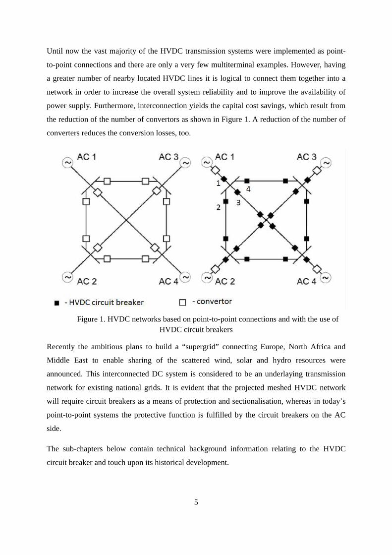
Until now the vast majority of the HVDC transmission systems were implemented as point-
to-point connections and there are only a very few multiterminal examples. However, having
a greater number of nearby located HVDC lines it is logical to connect them together into a
network in order to increase the overall system reliability and to improve the availability of
power supply. Furthermore, interconnection yields the capital cost savings, which result from
the reduction of the number of convertors as shown in Figure 1. A reduction of the number of
converters reduces the conversion losses, too.
Figure 1. HVDC networks based on point-to-point connections and with the use of HVDC circuit breakers
Recently the ambitious plans to build a “supergrid” connecting Europe, North Africa and
Middle East to enable sharing of the scattered wind, solar and hydro resources were
announced. This interconnected DC system is considered to be an underlaying transmission
network for existing national grids. It is evident that the projected meshed HVDC network
will require circuit breakers as a means of protection and sectionalisation, whereas in today’s
point-to-point systems the protective function is fulfilled by the circuit breakers on the AC
side.
The sub-chapters below contain technical background information relating to the HVDC
circuit breaker and touch upon its historical development.
6
1.1 General aspects
Implementation of an HVDC grid requires the availability of an HVDC circuit breaker that is
intended to protect the network. The HVDC circuit breakers are installed at the converter or
coupling substations to perform two major tasks [1]:
• Connection and disconnection of a convertor – CB 1 in Figure 1
• Connection and disconnection of the lines - CBs 2, 3 and 4 in Figure 1
The classification below covers the whole spectrum of failures typical for HVDC systems [2]:
• Internal converter faults:
- Malfunction of semiconductor valves
- Misfire and firethrough
- Commutation failure
- Short circuits within the convertor
• Short circuits on the DC transmission lines
• Faults on the AC side of a converter substation
An HVDC circuit breaker is supposed to operate not only to clear short circuits in DC
transmission lines, but also to disconnect the faulty converters and disconnect the DC network
from the short circuited AC system. According to statistics collected by the CIGRÉ
committee on HVDC and power electronics, the failure frequency (given as a percentage of
the total number of failures) in HVDC systems in 2010 was as follows [3]:
Short circuits on the transmission lines 9.2%
Converter faults 11.7%
DC equipment faults 14.6%
AC equipment faults 32.1%
Control system faults 21.6%
Other disturbances 10.8%
7
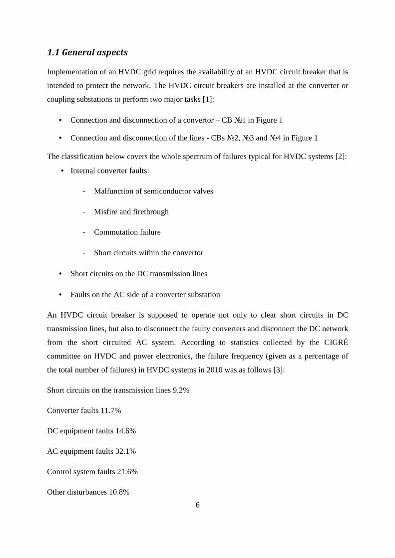
The absence of natural current transition through zero still remains a major stumbling block to
the development of an HVDC circuit breaker. Mechanical circuit breakers used in the AC
sector cannot be applied to DC switching directly because they rely on current zero, which is
the essential condition for extinction of the electric arc. For this reason, the problem of
designing a mechanical HVDC circuit breaker reduces mainly to developing a technique for
creation of an artificial current zero. Alternatively, DC switching by fully controllable
semiconductor devices is also possible.
The other peculiarity of the DC networks is that the fault currents are much higher than as
compared with the AC ones. The circuit inductance is active only in the transient state,
therefore the direct current is limited only by a very low circuit resistance. Figure 2 shows the
transmission line current before and after the pole-to-ground short circuit on a ±800 kV
HVDC link. As can be seen, right after the fault inception the current rises with the average
rate 210 A/ms. If not interrupted promptly, the high short-circuit current may overheat and
then damage the convertor equipment. Furthermore, a short circuit in the DC network is
associated with the voltage collapse, which may lead to destabilisation of the interconnected
AC grids. Therefore, the fast operating HVDC circuit breaker is preferred.
Figure 2. Short-circuit current development in LCC HVDC link
Regarding the HVDC CB itself, the flow chart in Figure 3 explains how the breaker design
benefits from the faster operation. However a faster breaker involves additional costs in its
turn due to a number of reasons, such as a more complex operating mechanism etc. This

8
discrepancy implies existence of the optimal operation time, therefore all pros and cons of fast
interruption must be carefully weighed.
Figure 3. Effect of interruption time on the HVDC CB costs
A high-voltage circuit breaker is triggered by a signal given by a protective relay. As known,
a relaying system requires certain time for the network condition analysis in order to identify
and correctly locate the fault. This fact means that in the HVDC CB development a time delay
after fault inception reserved for relaying must be taken into account. A well-proven
differential protection is used nowadays for the converter protection. However, there is
currently no available algorithm for the transmission line protection. The use of voltage and
current gradients of the travelling waves for fault detection is discussed, but the question
whether this approach is absolutely reliable still remains open. [2]
Based on the considerations above it can be concluded, that an HVDC circuit breaker must be
treated as a system component. Therefore, a systematic approach must be adopted to address a
challenging problem of HVDC CB development.
1.2 Literature review
The work on HVDC CB began even before the commissioning of the first commercially
operated HVDC systems already in 1940s [4], [5]. The wide-scale development of an HVDC
CB can be traced through the names of scientists from many countries. The research on
HVDC CB was conducted in the Soviet Union [6] and in the United States [7]. There are also
a great number of diverse publications on the topic written by Germans, French, Swiss and
Swedes. Japan developed an own HVDC industry for asynchronous and long-cable
interconnections between the islands. Japanese energy companies Toshiba and Hitachi had
9
intention to enter the HVDC switchgear market in 1980s [8], [9]. Iran, being interested in
nuclear technology, contributed with the research on the effectiveness of helical flux
compression generators as applied to HVDC CBs [10], [11]. Recently China got involved in
the development process as a new HVDC state [12].
The DC circuit breakers have been developed for many years not only for HVDC but also for
the other fields such as:
• Traction DC networks
• Power supplies of particle accelerators and fusion reactors [13], [14]
• Generator circuit breakers
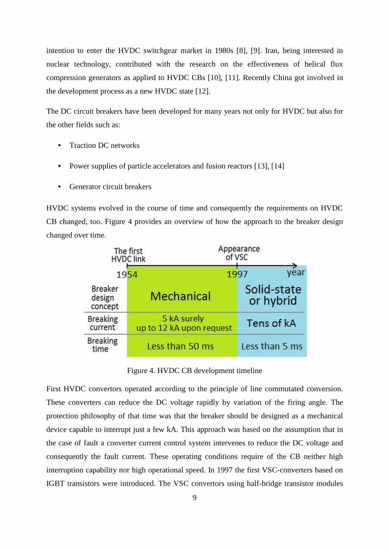
HVDC systems evolved in the course of time and consequently the requirements on HVDC
CB changed, too. Figure 4 provides an overview of how the approach to the breaker design
changed over time.
Figure 4. HVDC CB development timeline
First HVDC convertors operated according to the principle of line commutated conversion.
These converters can reduce the DC voltage rapidly by variation of the firing angle. The
protection philosophy of that time was that the breaker should be designed as a mechanical
device capable to interrupt just a few kA. This approach was based on the assumption that in
the case of fault a converter current control system intervenes to reduce the DC voltage and
consequently the fault current. These operating conditions require of the CB neither high
interruption capability nor high operational speed. In 1997 the first VSC-converters based on
IGBT transistors were introduced. The VSC convertors using half-bridge transistor modules

10
cannot limit the fault current on the DC side. As a result, extremely fast switching became a
requirement to protect the convertor from physical destruction by high short-circuit current.
Ekström et al. put forward the idea that the HVDC CB can be manufactured economically
only by using the components that standardised and available on the market [15]. Retracing
the historical development of an HVDC CB it can be noted, that initially the HVDC CB
concepts were designed with oil and air high-voltage switches. Then SF6 and vacuum devices
took over. Along with the progress in power electronics the power handling capability of
semiconductor devices grew significantly, giving a possibility to develop solid-state and
hybrid concepts. But nevertheless there are also known examples of designing the hardware
components primarily for HVDC circuit breakers. Below are a few of the numerous ones:
• Fast isolation switch of ABB [16]
Figure 5. Cross-section of fast isolation switch [16]
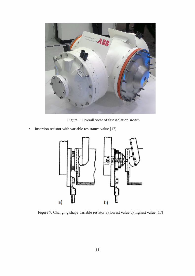
11
Figure 6. Overall view of fast isolation switch
• Insertion resistor with variable resistance value [17]
Figure 7. Changing shape variable resistor a) lowest value b) highest value [17]
12
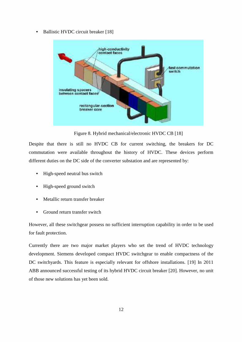
• Ballistic HVDC circuit breaker [18]
Figure 8. Hybrid mechanical/electronic HVDC CB [18]
Despite that there is still no HVDC CB for current switching, the breakers for DC
commutation were available throughout the history of HVDC. These devices perform
different duties on the DC side of the converter substation and are represented by:
• High-speed neutral bus switch
• High-speed ground switch
• Metallic return transfer breaker
• Ground return transfer switch
However, all these switchgear possess no sufficient interruption capability in order to be used
for fault protection.
Currently there are two major market players who set the trend of HVDC technology
development. Siemens developed compact HVDC switchgear to enable compactness of the
DC switchyards. This feature is especially relevant for offshore installations. [19] In 2011
ABB announced successful testing of its hybrid HVDC circuit breaker [20]. However, no unit
of those new solutions has yet been sold.
13
1.3 Research goals
The present thesis is meant to examine the technical and economic performance of different
HVDC CB concepts. The aim is to reveal the optimal HVDC CB concept for application in
the HVDC transmission grid.
Numerical simulations are employed as a main analysis tool to learn about the transient
phenomena in HVDC networks. The simulation studies on the electric circuits will be
complemented by consideration of the technical and economical constraints of the HVDC CB
concepts. These limitations are as follows:
• HVDC CB components weight, size and costs
• Operation time
• Magnitude of the arc voltage
• Interruption of the current with high di/dt
• Recovery voltage withstand of the open interrupter
The HVDC CB concepts under study will undergo a multiobjective parameter optimisation in
order to get an estimation of their potential breaking capabilities.
In addition, the issue of CB-network interaction will be studied. The questions to be clarified
are:
• Switching overvoltages
• Necessity for closing/opening resistors, grading capacitors and fault current limiters
The outcomes of the present work are intended to serve as the suggestions for the
development and the construction of a working test circuit breaker.

14
1.4 Thesis overview
This thesis consists of six chapters and is organised as follows:
• Chapter 2 touches upon the issue of general requirements to an HVDC circuit breaker
and contains a detailed description of DC switching techniques. The sub-chapters
introduce the concepts of HVDC circuit breakers and provide theoretical analysis of
their operation.
• Chapter 3 outlines the theory of the electric arc physics with regard to SF6 and
vacuum media. It describes also modelling procedures for SF6 and vacuum
interrupters and for the semiconductor switches.
• Chapter 4 presents a simulation-based performance evaluation for different HVDC CB
concepts. The economic aspects and the selection criteria for circuit breaker
components are covered, too.
• Chapter 5 discusses supplementary questions regarding fault protection for an HVDC
network. It handles also the issues of system stability as applied to the use of fault
current limiters.
• Chapter 6 summarises the results achieved and gives recommendations for future
work.
15
2 Methods of direct current interruption
To date, a host of HVDC CB concepts have been developed. Some of those concepts exist
only on paper; the others, being implemented, still remain nothing but successfully tested
exemplars. In particular it can be explained by the fact that the HVDC CB is not a technology
in great demand but a solution for the foreseeable future of transmission grids. Furthermore,
the HVDC CB is not the only one obstacle on the way towards HVDC grid. There are still a
range of open questions regarding power flow control in a meshed DC network, reliable
relaying solution, standardisation etc. Therefore, an HVDC CB must be developed not as a
single component but in conjunction with the other related aspects.
This chapter is based on a review of different DC switching techniques and discusses a set of
requirements that an HVDC CB must comply with.
2.1 Requirements to HVDC breakers
An HVDC circuit breaker must fulfill a number of sometimes contradictive requirements.
Only such abstract thing as an ideal switch can possess all those features. Therefore, the
partial fulfilment of what is required in order to attain the golden mean is desirable. The list of
requirements is presented below.
• Sufficient current breaking capability is required to clear all prospective faults.
• Fast operation is required to protect the equipment and quickly restore normal
network operation.
• Minimal on-state losses make the breaker economical and the cooling system
unnecessary.
• Permissible overvoltages must be secured. The switching overvoltages must be
limited down to 160% of the rated system voltage. [21], [22]
• Overload capability is required, since overload is a not infrequent situation for
transmission networks.
• Bidirectional current flow should be expected in complex networks. If the
breaker is not bidirectional, then two antiparallel-connected units have to be
provided.

16
• Lightness and compactness are often required for the offshore installation.
• Reclosing capability is required to enable fast restoration of power supply in the
case of transient faults.
• Simplicity is required to make the breaker cheaper and reduce maintenance costs.
• Modular design enables scalability, fast assembly, easy repair and shipping.
• Reliability
• Eco-friendliness
2.2 Existing HVDC-breaker concepts
All the variety of HVDC circuit breakers can be classified as power electronics based,
mechanical and hybrid solutions. This chapter contains a review of different approaches to
breaking of direct current and covers all three above-mentioned groups. Sub-sections describe
configurations of the circuit breakers employing certain principle of operation and give a
theoretical basis for the technical analysis.
An HVDC circuit breaker is a complex technical arrangement consisting of the main
switching element and its auxiliary components. These auxiliaries may fulfil different
functions such as assisting the main switch in the current interruption or providing recovery
voltage withstand after breaking.
HVDC circuit breakers may either require or not the condition of current passage through
zero value depending on the main switch employed in the breaker. The table below contains a
systematised information on current interruption techniques in DC circuits according to
CIGRÉ for the cases in which current zero is a prerequisite to circuit breaker operation.
17
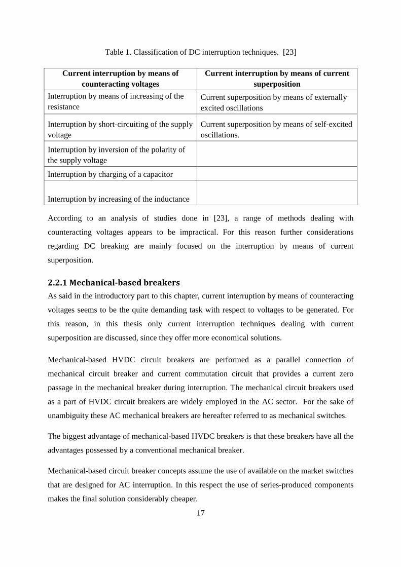
Table 1. Classification of DC interruption techniques. [23]
Current interruption by means of counteracting voltages
Current interruption by means of current superposition
Interruption by means of increasing of the resistance
Current superposition by means of externally excited oscillations
Interruption by short-circuiting of the supply voltage
Current superposition by means of self-excited oscillations.
Interruption by inversion of the polarity of the supply voltage
Interruption by charging of a capacitor
Interruption by increasing of the inductance
According to an analysis of studies done in [23], a range of methods dealing with
counteracting voltages appears to be impractical. For this reason further considerations
regarding DC breaking are mainly focused on the interruption by means of current
superposition.
2.2.1 Mechanical-based breakers
As said in the introductory part to this chapter, current interruption by means of counteracting
voltages seems to be the quite demanding task with respect to voltages to be generated. For
this reason, in this thesis only current interruption techniques dealing with current
superposition are discussed, since they offer more economical solutions.
Mechanical-based HVDC circuit breakers are performed as a parallel connection of
mechanical circuit breaker and current commutation circuit that provides a current zero
passage in the mechanical breaker during interruption. The mechanical circuit breakers used
as a part of HVDC circuit breakers are widely employed in the AC sector. For the sake of
unambiguity these AC mechanical breakers are hereafter referred to as mechanical switches.
The biggest advantage of mechanical-based HVDC breakers is that these breakers have all the
advantages possessed by a conventional mechanical breaker.
Mechanical-based circuit breaker concepts assume the use of available on the market switches
that are designed for AC interruption. In this respect the use of series-produced components
makes the final solution considerably cheaper.
18
The distinguishing feature of a mechanical circuit breaker is its moderate power losses and
when carrying continuous current, as a consequence, the absence of cooling requirement. It is
more stable to overloads as compared with semiconductor switches. Mechanical breakers can
be located outdoors. The possibility of bidirectional current flow is also significant amongst
the other advantages of this breaker.
The necessity of current transition through zero value to enable arc extinction and hence
current interruption in the circuit, can be regarded as the major drawback of mechanical
circuit breakers. In order to fulfill the preconditions for arc quenching artificial current zeroes
must be produced.
Disadvantages other than those linked with the need for current zero relate to the operating
speed of mechanical switches. If compared with the power electronic switches, a mechanical
breaker is inferior in the speed of operation which leads to increased breaking current under
short-circuit conditions.
In current superposition techniques the resultant current to be interrupted is the sum of the
breaking direct current and the alternating current or current impulse superimposed by some
oscillating circuit connected in parallel to mechanical switch. The nature of oscillations
excited by the oscillating circuit is classified below:
• Self-induced oscillations
• Oscillations resulting from non-equilibrium initial conditions
• Forced oscillations
• Parametric oscillations
The following four sub-sections describe each oscillation type putting aside the issue of its
practical feasibility. A simple qualitative analysis of each oscillation type is carried out and
limitations of each oscillation type are discussed.
2.2.1.1 Passive-type resonance breaker
A passive resonance HVDC circuit breaker consists of a mechanical switch and a parallel-
coupled oscillating circuit composed of capacitor and inductor as shown in Figure 9.

19
Figure 9. Arrangement of the passive resonance HVDC CB
This type of HVDC circuit breaker was for the first time reported in [6] and works as follows.
As soon as the mechanical switch starts to open its contacts, an electric arc arises between
them, and resonance occurs in the loop formed by mechanical switch, inductor and capacitor.
This phenomenon is possible owing to the electric arc property of displaying negative
differential resistance.
Resonance developing within the HVDC circuit breaker entails increase in the magnitude of
the current oscillating in the L-C circuit. This current being superimposed on the breaking
current provides current zero and enables the mechanical switch to quench the arc.
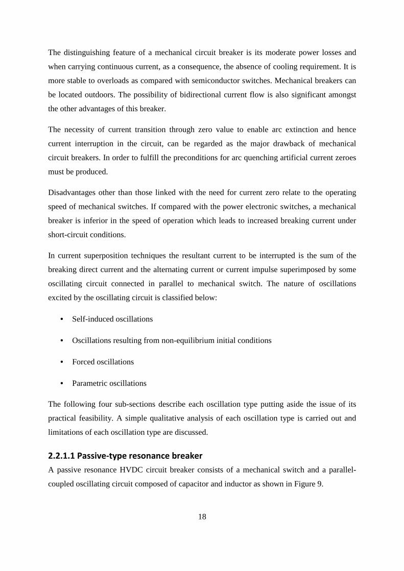
According to Kirchhoff’s voltage law written for the loop made up of mechanical breaker,
inductor and capacitor, valid:
arcCL uuu =+ (1)
As known, arc voltage is a non-linear function of current:
( )arcarc ifu = (2)
Applying current-voltage relations for inductor and capacitor:
arc
t
cc udtti
Cdt
tdiL =⋅⋅+⋅ ∫
∞−
)(1)(
(3)
Differentiating equation (3):
20
dt
tduti
Cdt
tidL arc
cc )(
)(1)(
2
2
=⋅+⋅ (4)
Time derivative of the arc voltage can be expanded:
dt
tdi
di
idu
dt
tidu
dt
tdu arc
arc
arcarcarcarcarc )()())(()(⋅== (5)
Arc voltage derivative with respect to current is called the differential resistance:
arc
arcarcdiffarc di
iduR
)(= (6)
This differential resistance represents the slope of the i-u arc characteristic at a certain point.
Assuming that the system surge impedance is infinite, the oscillating current is confined
within the oscillating loop. That means also:
dt
tdi
dt
tdi carc )()(−= (7)
Substitution of (5) and (6) into (4) gives:
0)(1)()(
2
2
=⋅+⋅+⋅ tiCdt
tdiR
dt
tidL c
cdiffarc
c (8)
The oscillating circuit consisting of mechanical switch, inductor and capacitor is described by
the second-order linear differential equation. The characteristic equation for (8) is written as:
( ) ( ) 012 =+⋅+⋅C
irRirL cdiffarcc (9)
Where:
r – differential operator
The differential arc resistance diffarcR is a function of the capacitor current, which is the
argument in equation (8). For the purpose of making further analysis more simple, the
breaking process will be considered in the restricted current band.
This stipulation gives a possibility to assume the differential arc resistance being constant.

21
Current oscillations in the circuit take place only when periodic functions of sine and cosine
are present in the solution of the equation (8). That means that the roots of its characteristic
equation must be complex, hence, the following inequality must hold:
C
LRdiff
arc 2< (10)
Applying initial conditions Ic(0 ) = 0, Uc(0) = 0, UL(0) = Uarc(0), the solution of (8) is as follows:
( )teL
Uti tarc
c ⋅⋅⋅⋅
= − ωω
δ sin)0(
)( (11)
Where:
Uarc(0) – arc voltage that corresponds to the breaking current
L
Rdiffarc
2=δ - damping coefficient
( ) 2202
2
4
1 δωω −=−⋅
=L
R
CL
diffarc
- resonant angular frequency
CL ⋅= 1
0ω - ideal resonant angular frequency
From the solution analysis for the extreme cases follows:
• If C is infinite, then no current oscillations take place, because the breaking current is
entirely commutated to the capacitor. But in general, the larger the capacitance the
more pronounced current oscillations occur. That means greater C increases the
interruption capability.
• If L is large, current oscillations are initiated, but the initial oscillation amplitude and
the rate of rise of oscillations are quite low. This can be seen from (11) and from the
formula of the damping coefficient. The first current zero may occur several tens of
milliseconds after the breaking initiation.
22
• If L and C are very small the circuit does not generate oscillations.
Equation (11) also shows that the amplitude of the initial oscillation is proportional to the
arcing voltage corresponding to the breaking current. At high breaking currents the initial
oscillation is weak because the arc voltage is low. Furthermore, at high currents the arc
differential resistance becomes low in magnitude. This decreases the damping coefficient and
results in a low rate of rise of oscillations. It is to be remembered, that the damping coefficient
has a negative value, since the electric arc at high currents has a negative differential
resistance. Starting with low magnitude and having a low rate of rise, the oscillation will
reach current zero only at a substantial time after breaking initiation. This fact makes this
circuit breaker concept inappropriate for breaking of high currents.
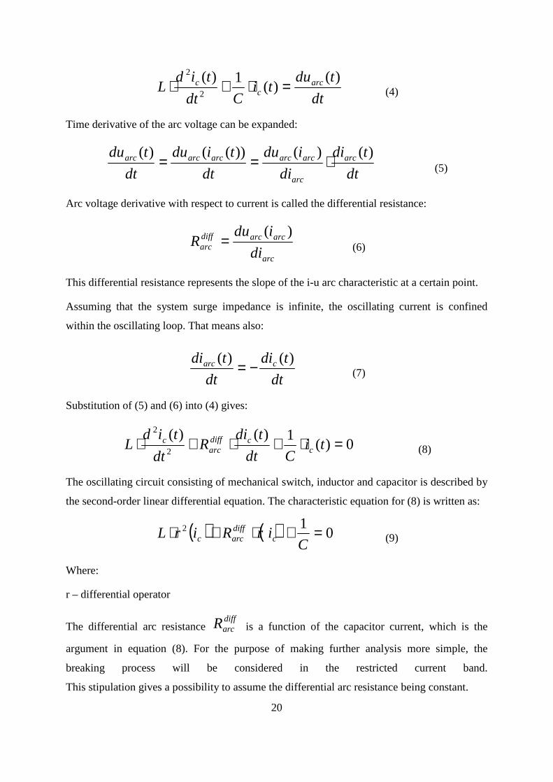
2.2.1.2 Active-type resonance breaker
As noted in the section devoted to the passive resonance breaker, its breaking capability is
dependent on the arc properties and decreases as the breaking current becomes higher. In this
situation an active concept may offer a better current interruption performance, because an
active HVDC CB incorporates a pre-charged capacitor, which can store more energy than that
which could be withdrawn from the DC network by means of transients in the passive
solution. The active circuit breaker concept is depicted in Figure 10 and works according to
the principle of free oscillations, originating from the initially non-equilibrium state of the
oscillating circuit.
Figure 10. Circuit diagram of the active resonance HVDC CB with commutation switch CS

23
When the active breaker performs a breaking operation, the main mechanical switch opens
and the auxiliary switch CS or triggerable spark gap in the oscillatory circuit connects the L
and C elements in series as shown in the Figure 10. At the moment when the oscillatory loop
is formed, the capacitor starts to recharge generating current impulse, which is superimposed
on the current to be broken. A higher counter-current magnitude increases breaking capability
and simultaneously decreases the breaking time of the circuit breaker.
Physically the difference between passive and active resonance breakers is in the initial
conditions of the oscillating circuit. The capacitor is pre-charged rather than having zero
voltage between the plates. The descriptive relations and computation procedure are the same.
Applying initial conditions Ic(0) = 0, Uc(0) = Uc(0),
UL(0) = Uarc(0) + Uc(0), the solution of (8) is as follows:
( )teL
UUti tcarc
c ⋅⋅⋅+
= − ωω
δ sin)0()0(
)( (12)
As compared with (11), the initial oscillation amplitude of ic(t) is higher thanks to Uc(0).
The magnitude of the oscillation in the L-C-breaker circuit is determined from (12) as:
L
UUti carc
cω
)0()0()(
^ += (13)
The arc current is accordingly:
( ) ( )teL
UUtiti tcarc
arc ⋅⋅⋅+
−= − ωω
δ sin)0()0(
)( (14)
Where:
i(t) – breaking current
From (13) is evident that the counter-current magnitude depends only on the capacitor
charging voltage and circuit reactance and is not a function of the capacitor size. Capacitance
along with inductance determines the current impulse frequency.
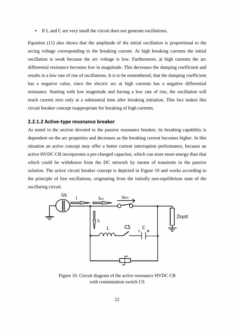
Implementation of this DC breaking principle requires that a special capacitor charging setup
should be foreseen. Pre-charging from the line voltage seems to be the most practical solution.
Schematically this principle is illustrated in Figure 11.
24
Figure 11. Charging equipment of the commutation capacitor
This DC breaking approach is realised in ITER for current switching in the central solenoid
coil. In this particular example the current of 170 kA is shared by four parallel units each
consisting of vacuum interrupter and oscillatory circuit. [13], [14]
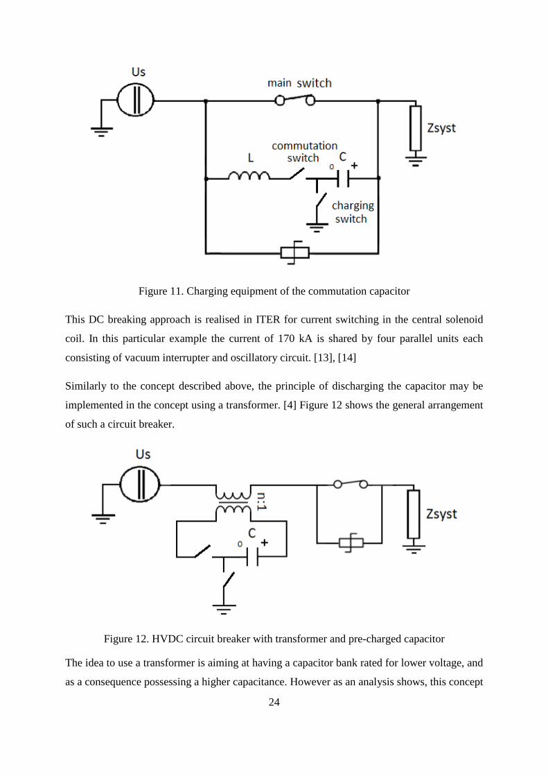
Similarly to the concept described above, the principle of discharging the capacitor may be
implemented in the concept using a transformer. [4] Figure 12 shows the general arrangement
of such a circuit breaker.
Figure 12. HVDC circuit breaker with transformer and pre-charged capacitor
The idea to use a transformer is aiming at having a capacitor bank rated for lower voltage, and
as a consequence possessing a higher capacitance. However as an analysis shows, this concept

25
can be suitable only for circuits with a very small amount of stored magnetic energy.
Otherwise the component size becomes prohibitive. [17]
2.2.1.3 Forced oscillations in DC breaking
The circuit breakers introduced in the two preceding sections are based on the principle of
free current oscillations. The breaker concept described in the present section uses forced
oscillations excited by an auxiliary source of power. The outline of this circuit breaker is
demonstrated in Figure 13.
The circuit breaker is conceived as a parallel coupling of mechanical switch and oscillatory
circuit, which includes the serially connected inductor, capacitor and transformer winding.
The other transformer winding is powered by alternating voltage source. The voltage source
frequency matches with the resonant frequency defined by the reactive components.
The considered approach of creating a current zero is advantageous over the self-excited one
in respect that the breaking capability does not rely upon the electric arc properties. Unlike the
active resonance breaker, the concept in question is expected to have considerably higher
interruption capability, because at forced resonance the circuit reactance becomes zero and the
current is limited only by the oscillating circuit parasitic resistance and active arc resistance.
Figure 13. Topology of the HVDC CB with externally powered oscillating circuit
As in any other oscillating breaker type, the resultant arc current constitutes a superposition of
the breaking DC current and AC current induced in the oscillating circuit. The forced
oscillations in the linear circuit are described by the linear differential equation:

26
( ) ( )tpEtiCdt
tdiR
dt
tidLL c
cdiffarc
c ⋅⋅=+⋅+⋅+ sin)(1)()(
2
2
σ (15)
Where:
Lσ – leakage inductance of the transformer
E – magnitude of the externally supplied voltage
p – angular frequency of the externally supplied voltage
The effect of resonance takes place when the capacitive and inductive reactances are equal.
This means that the total circuit reactance is zero.
CLLXXX cL ⋅
−+⋅=+=ω
ω σ1
)( (16)
Solving the nonhomogeneous linear differential equation (15) using the method of
undetermined coefficients yields the general solution for the current:
( )
( ) ( ) ( )
( ) diffarc
diffarc
tarcc
RpLLpC
tpRptpLLpC
E
teL
Uti
222
2
2
1
cossin1
sin)0(
)(
⋅+
+⋅−
⋅⋅⋅−⋅
+⋅−⋅+
+⋅⋅⋅= −
σ
σ
δ ωω
(17)
Solution (17) is valid for the restricted current range only, because it is gained on the
assumption that the differential arc resistance is a constant coefficient.
From the expression (17) it can be seen that current oscillations will happen at a fundamental
frequency p, defined by the source. A fundamental current curve will be superimposed by
weak oscillations at natural resonant frequency determined by L-C parameters of the
commutation circuit.
As applied to the high-current region, where differential arc resistance is very close to zero
and can be neglected, the solution (17) degenerates into the equation of easier form:

27
( ) ( )( )
+⋅−
⋅⋅
⋅⋅+⋅⋅=
σ
ωω
LLpCp
p
tpEt
L
Uti arc
c1
sinsin
)0()(
(18)
In the expression (18) the difference in the denominator is zero according to (16) and this fact
leads to an infinite growth of current as a result of resonance. It can be also seen that a higher
source voltage and lower forced oscillation frequency contribute to a higher oscillation
magnitude.
2.2.1.4 Parametric oscillations in DC breaking
Suggested in this section an approach to DC breaking uses the phenomenon of energy
pumping into the oscillating circuit, wherein the values of the reactive components, namely
capacitance and inductance, change periodically. Figure 14 displays the circuit topology of
such a circuit breaker.
Figure 14. Arrangement of the HVDC CB with periodically varying reactive components
The circuit breaker design is similar to the other concepts employing the principle of current
superposition, except that L and C can be varied. An oscillatory system becomes instable
when the resonance circuit is initially excited by the pulse of arcing voltage due to the
opening of the mechanical switch and then further excited by periodic variation of some
reactive parameter. If the parameter variation frequency concurs with the natural oscillation
28
frequency of the resonant circuit, the oscillatory system starts drifting from equilibrium state
in oscillating manner with progressively increasing amplitude. This phenomenon is referred to
as parametric resonance.
Parametric oscillations are possible in any oscillatory system. For instance in series LCR-
circuit oscillations can be excited by varying the capacitance with the help of periodical
moving of capacitor plates near and apart.
In order to achieve a parametric resonance the capacitance must decrease stepwise when the
energy accumulated therein is maximal and equal to the whole energy contained in the circuit.
At this moment circuit energy content increases owing to the force acting on the capacitor and
pulling apart its plates. A quarter-period later when the capacitor is discharged and contains
no energy the capacitance value must increase stepwise back to the initial value. At that
moment the energy contained in the circuit remains unchanged. This procedure is repeated
periodically and energy is pumped into the circuit through the capacitor twice a period. When
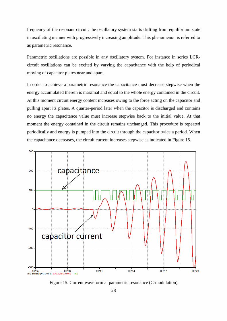
the capacitance decreases, the circuit current increases stepwise as indicated in Figure 15.
Figure 15. Current waveform at parametric resonance (C-modulation)

29
A similar effect can be achieved by an inductance modulation by means of periodical moving
of the reactor core inwards and outwards. A simultaneous modulation of two parameters using
different strategies is also possible [24].
For the circuit depicted in Figure 14 holds true:
0=−+ arcCL uuu (19)
The voltages of the components are functions of the time-dependant capacitor current and
capacitor charge. Thus we get:
( ) 0)(1)(
2
2
=⋅++⋅ tqC
tudt
tqdL carc
c (20)
Where:
qc(t) – capacitor charge
The arc voltage can be written as follows:
( ) ( )( ) ( )( ) ( )titiRtiutu arcarcarcarcarcarc ⋅== (21)
In accordance with Kirchhoff’s current law:
( ) ( ) ( )tititi carc −= (22)
Where:
i(t) – breaking current
Substitution of (21) and (22) into (20) and rearrangement of terms give:
( )( ) ( )( ) ( )titiRtqCdt
dqtiR
dt
tqdL arcarcc
carcarc
c ⋅=⋅+⋅+⋅ )(1)(
2
2
(23)
Equation (23) is a complex differential equation with non-constant coefficients, which is
difficult to solve analytically. However, applying numerical methods a solution for the current
as demonstrated in Figure 15 can be obtained.

30
The modulation index describes to which extent the modulated variable value varies around
its unmodulated level. Owing to energy dissipation in circuit resistance, parametric resonance
is possible only at certain values of the modulation index, at which the energy input into the
circuit prevails over energy dissipation in the circuit. Furthermore the modulation of a certain
parameter cannot turn into action oscillator, which is in a motionless equilibrium state. In
order to enable parametric resonance, as opposed to forced resonance, in the oscillatory
system at least weak initial oscillation must be available.
2.2.2 Circuit breaker incorporating semiconductor devices
HVDC circuit breakers incorporating power electronic switches take advantage of their fast
switching capability. These semiconductor switches may serve as a main switch or as a part of
auxiliary circuit intended for current commutation. Conventionally HVDC circuit breakers
using semiconductors can be divided into two groups:
• Solid-state circuit breakers
• Hybrid circuit breakers
The semiconductor devices can be classified into three groups depending on their switching
functionality: non-controllable switches, semi-controllable switches and fully controllable
switches. Table 2 presents an overview of power semiconductors that potentially can be used
in an HVDC circuit breaker. The current and voltage ratings given in the table do not describe
the same device but correspond to the highest achievable values for the devices of specified
type. As a rule, the higher the rated blocking voltage, the lower is the rated continuous current
and vice versa.

31
Table 2.Overview of power semiconductors applicable for HVDC
Device type Continuous current Blocking voltage
Non-controllable switches
Diode 7385 A 6 kV
Semi-controllable switches
Thyristor 5000 A 12 kV
Fully controllable switches
GTO 6000 A 6 kV
IGCT 3000 A 6.5 kV
IGBT 3600 A 6.5 kV
Apart from the very short switching time, the ability to switch off without necessity for
current zero is the other positive feature of fully controllable semiconductors. Fully
controllable switches are represented by power transistors of any type and power thyristors
that can be turned off by a gate signal.
A drawback of semiconductor devices is their increased power losses as compared to the
mechanical switches. The power dissipation of switching device is given by the sum:
gswond PPPP ++= (24)
Where:
Pon – on-state power losses
Psw – switching power losses
Pg – gate power losses
On-state power losses result from the small voltage drop across the device in a conduction
mode. During the switching phase both current and voltage magnitudes are in the transition
between zero and the operating value. The product of current and voltage gives instantaneous
switching losses. The switching losses predominate over the conduction losses in applications
with high switching frequency, for example in hard-switching converters. The gate power is
32
comparatively low and is usually not taken into consideration. The heat energy generated in
the device, if not taken off, may overheat and finally harm its p-n junctions. Therefore, power
dissipation by means of heat sinks or active water cooling must be foreseen.
The requirement for safe operation of power semiconductor imposes a limitation on the rate
of rise of current through the switch at turning on and the limitation on the rate of rise of
recovery voltage across the switch at turning off. Overstresses caused by the high values of
di/dt and du/dt may lead to a physical damage of the device. Semiconductor switches are
often equipped with the snubber circuits, thereby mitigating the conditions of commutation.
The following two sub-sections give a description of the HVDC CB employing
semiconductor devices. In addition a brief analysis of a circuit breaker-electric network
interaction is presented.
2.2.2.1 Solid-state HVDC circuit breakers
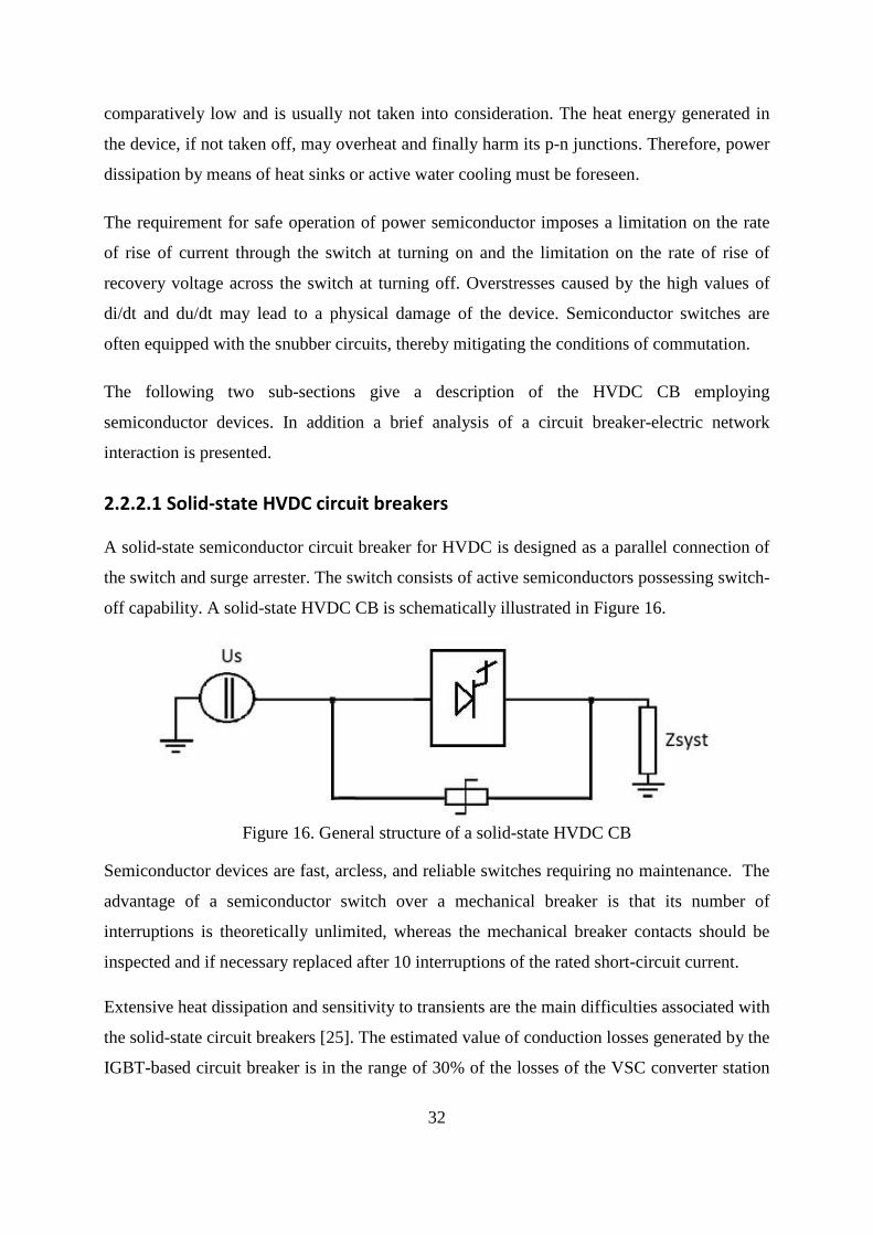
A solid-state semiconductor circuit breaker for HVDC is designed as a parallel connection of
the switch and surge arrester. The switch consists of active semiconductors possessing switch-
off capability. A solid-state HVDC CB is schematically illustrated in Figure 16.
Figure 16. General structure of a solid-state HVDC CB
Semiconductor devices are fast, arcless, and reliable switches requiring no maintenance. The
advantage of a semiconductor switch over a mechanical breaker is that its number of
interruptions is theoretically unlimited, whereas the mechanical breaker contacts should be
inspected and if necessary replaced after 10 interruptions of the rated short-circuit current.
Extensive heat dissipation and sensitivity to transients are the main difficulties associated with
the solid-state circuit breakers [25]. The estimated value of conduction losses generated by the
IGBT-based circuit breaker is in the range of 30% of the losses of the VSC converter station
33
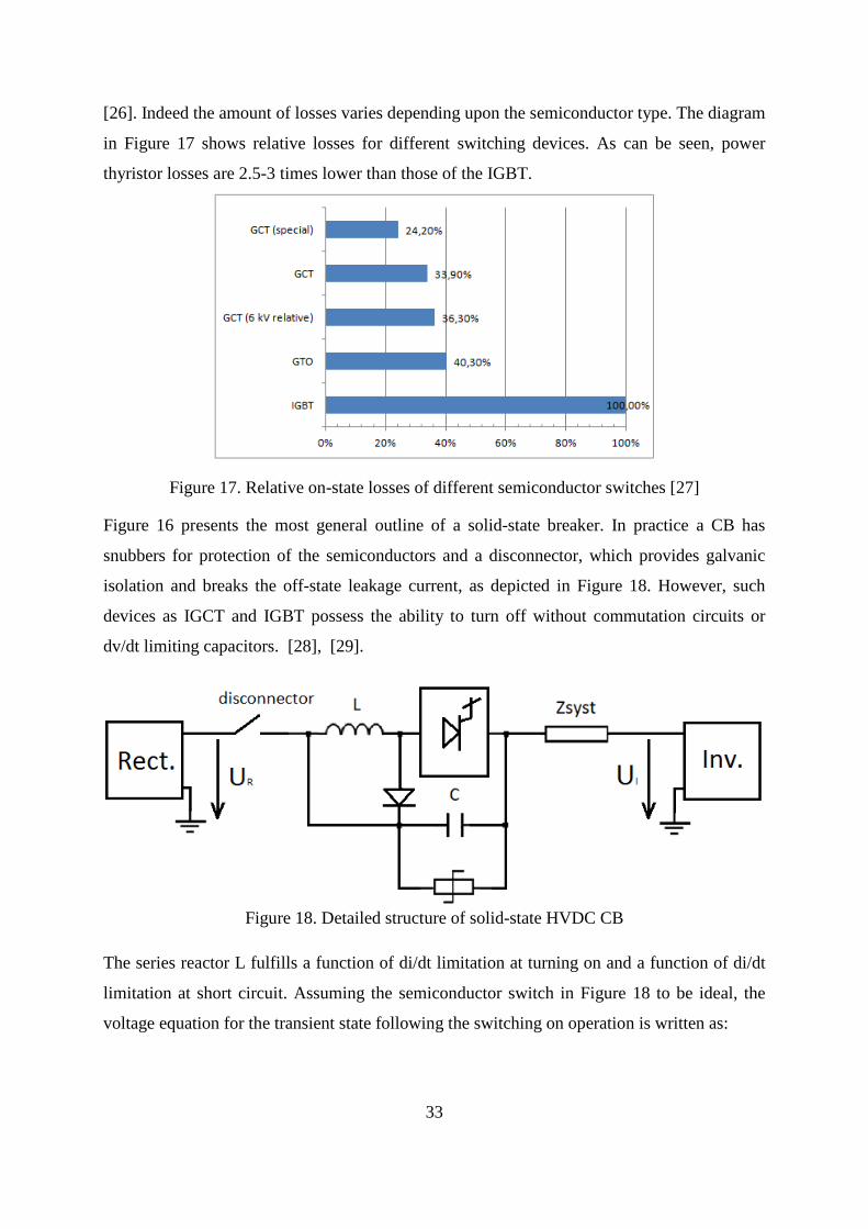
[26]. Indeed the amount of losses varies depending upon the semiconductor type. The diagram
in Figure 17 shows relative losses for different switching devices. As can be seen, power
thyristor losses are 2.5-3 times lower than those of the IGBT.
Figure 17. Relative on-state losses of different semiconductor switches [27]
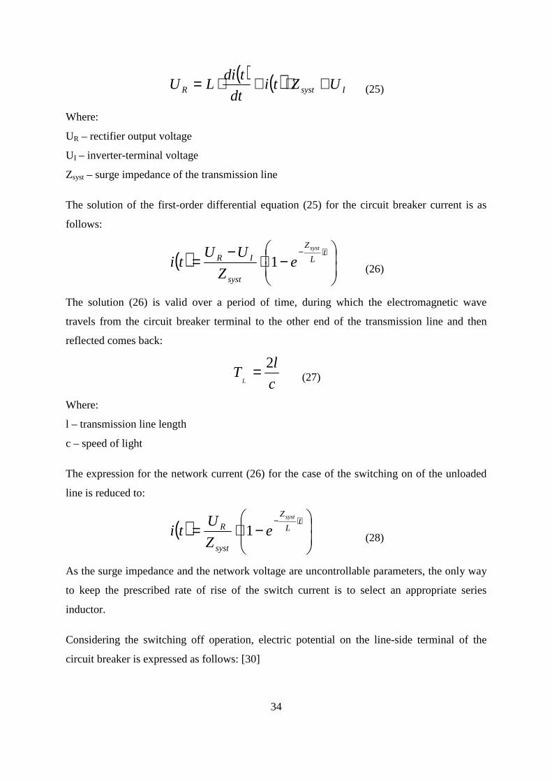
Figure 16 presents the most general outline of a solid-state breaker. In practice a CB has
snubbers for protection of the semiconductors and a disconnector, which provides galvanic
isolation and breaks the off-state leakage current, as depicted in Figure 18. However, such
devices as IGCT and IGBT possess the ability to turn off without commutation circuits or
dv/dt limiting capacitors. [28], [29].
Figure 18. Detailed structure of solid-state HVDC CB
The series reactor L fulfills a function of di/dt limitation at turning on and a function of di/dt
limitation at short circuit. Assuming the semiconductor switch in Figure 18 to be ideal, the
voltage equation for the transient state following the switching on operation is written as:
34
( ) ( ) IsystR UZtidt
tdiLU +⋅+⋅= (25)
Where:
UR – rectifier output voltage
UI – inverter-terminal voltage
Zsyst – surge impedance of the transmission line
The solution of the first-order differential equation (25) for the circuit breaker current is as
follows:
( )
−⋅
−=
⋅− tL
Z
syst
IRsyst
eZ
UUti 1 (26)
The solution (26) is valid over a period of time, during which the electromagnetic wave
travels from the circuit breaker terminal to the other end of the transmission line and then
reflected comes back:
c
lT
L
2= (27)
Where:
l – transmission line length
c – speed of light
The expression for the network current (26) for the case of the switching on of the unloaded
line is reduced to:
( )
−⋅=
⋅− tL
Z
syst
Rsyst
eZ
Uti 1 (28)
As the surge impedance and the network voltage are uncontrollable parameters, the only way
to keep the prescribed rate of rise of the switch current is to select an appropriate series
inductor.
Considering the switching off operation, electric potential on the line-side terminal of the
circuit breaker is expressed as follows: [30]

35
( ) ( )
−⋅⋅−⋅⋅= ⋅
−CZ
t
systsystsysteCZt
dt
tdiZte 1
(29)
Where:
( )dt
tdi - slope of the current before interruption
Expression (29) holds true for the time determined by (27). Differentiation of (29) yields the
rate of rise of recovery voltage (RRRV) across the circuit breaker:
( ) ( )
−⋅⋅= ⋅
−CZ
t
systsyste
dt
tdiZ
dt
tdu1
(30)
Expression (30) shows, that the rate of rise of recovery voltage across the opened switch is
mainly dependent upon the slope of the current before interruption and the volume of the
snubber capacitor. Any transistor is an amplifier device, which allows controlling of the large
collector currents by a small gate current or voltage [28]. Theoretically, this feature of a
transistor gives a possibility to perform slower interruption using the gate signal. However,
slower switching leads to increased power dissipation, which may finally destroy the device.
Therefore, the possibility of slower switching should be assessed using an adequate transistor
model.
Active semiconductor switches are mostly the unidirectional devices, which can conduct
current only in one direction. For this reason, in the networks where power flow direction may
change, modifications in the circuit breaker topology must be introduced. Figure 19
demonstrates two alternative solutions. Topology a) uses two anti-parallel branches of
switching elements; topology b) is based on the diode bridge, which directs current from the
anode to the cathode of the main switch.
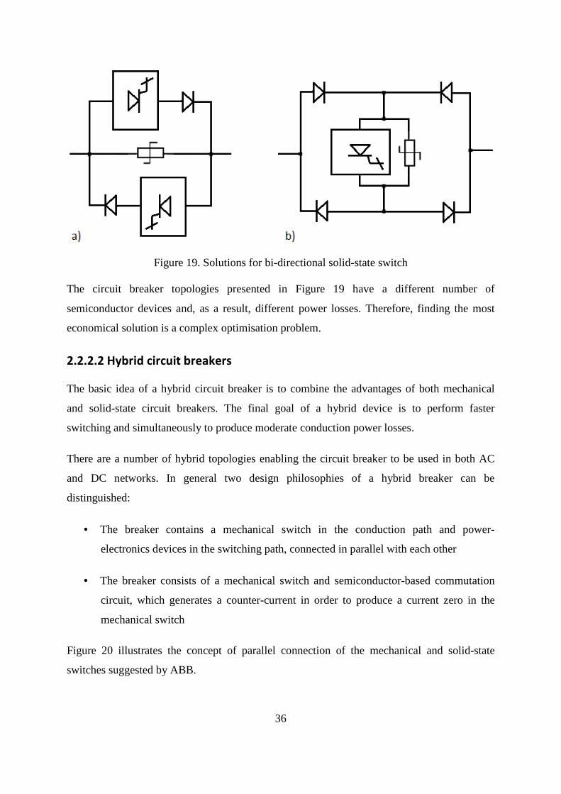
36
Figure 19. Solutions for bi-directional solid-state switch
The circuit breaker topologies presented in Figure 19 have a different number of
semiconductor devices and, as a result, different power losses. Therefore, finding the most
economical solution is a complex optimisation problem.
2.2.2.2 Hybrid circuit breakers
The basic idea of a hybrid circuit breaker is to combine the advantages of both mechanical
and solid-state circuit breakers. The final goal of a hybrid device is to perform faster
switching and simultaneously to produce moderate conduction power losses.
There are a number of hybrid topologies enabling the circuit breaker to be used in both AC
and DC networks. In general two design philosophies of a hybrid breaker can be
distinguished:
• The breaker contains a mechanical switch in the conduction path and power-
electronics devices in the switching path, connected in parallel with each other
• The breaker consists of a mechanical switch and semiconductor-based commutation
circuit, which generates a counter-current in order to produce a current zero in the
mechanical switch
Figure 20 illustrates the concept of parallel connection of the mechanical and solid-state
switches suggested by ABB.

37
Figure 20. Hybrid HVDC CB – concept of ABB [31]
During normal operation the current flows only through the path formed by the fast
mechanical disconnector FMD and semiconductor-based commutation switch. At switching
off the commutation switch commutates the current into the main switch, then the fast
mechanical disconnestor opens providing sufficient isolation, and finally the main switch
interrupts the current. Lower power dissipation results from the low contact resistance of the
FMD and the low resistance of a commutation switch, which includes only a few
semiconductors.
The alternative to the hybrid HVDC breaker concept of ABB is shown in Figure 21.
Figure 21. Hybrid HVDC CB – alternative concept
In normal operation the load current is shared between two parallel branches formed by
mechanical switches MS1-MS2 and MS3-MS4. During switching off, switches MS2 and
MS3 open first, commutating the whole current into the semiconductor switch. Then the
semiconductor switch interrupts the current, and finally MS1 and MS4 open in order to

38
provide galvanic isolation. Should the current flow in the opposite direction, the switches
MS1 and MS4 would open first.
In the concepts described above the switching operations performed by the main switch
resemble the operation of a solid-state circuit breaker. Therefore all considerations regarding
transients, which initiate from the commutation processes and discussed in the previous sub-
section, are valid for these hybrid breakers, too.
Figure 22 presents two possible configurations of the hybrid HVDC breakers with a
commutation circuit. In these breakers an approach of two-stage commutation is realised. In
the first stage the mechanical switch is tripped, the commutation circuit induces a counter-
current impulse, which aims at producing a current zero. Following arc extinction in the main
switch, the breaking current is commutated in the current limiting resistor. In the second stage
the recharged capacitor causes reverse-biasing of the thyristor T2 and T1 in the scheme a) and
b) correspondingly. As soon as the negative voltage is applied across the thyristors T2 and T1
in schemes a) and b) they are enabled to switch off and finally the DC current is blocked by
the capacitor itself.
Figure 22. Two-stage hybrid circuit breakers [25], [32]
In contrast to the concepts of ABB and the alternative one, the breakers in Figure 22
demonstrate longer switching times. Analytical analysis of the operation of these two-stage
circuit breakers is a complex task; therefore numerical simulation is recommended as a less
demanding alternative. Hybrid medium-voltage DC breakers with parallel commutation
circuits are produced commercially by several companies using air and vacuum mechanical
switches [25].

39
3 Modelling
The primary aim of the present study is to assess the technical effectiveness of different
HVDC circuit breakers. The main characteristics that need to be examined are the current
breaking capability and the breaking speed, which are the indicators of the commutation
performance. Every commutation in an electric circuit is a dynamic process.
Investigation of the transient behaviour of the complex electric systems can be simplified by
resorting to the help of digital simulation. The simulation results give insight into the system
behaviour for the specified time interval, whereas the system under study is described by its
model realised in a simulation environment. In the simulation of electric systems the real
circuit components are represented by their equivalent models.
In the present work simulations were conducted with the use of the ATP-EMTP software.
ATP-EMTP serves to solve the system of differential equations describing the circuit to be
simulated. Solving is executed by means of the numerical methods applying the trapezoidal
rule of integration.
ATPDraw is a graphical preprocessor to the ATP-EMTP intended for graphical construction
of an electric circuit using the library of the electric components. ATPDraw includes also
supporting sub-routines, which calculate electric parameters of transmission lines, electric
machines, transformers and other complex equipment based on the design and operational
data. The supporting sub-routine MODELS enables the user to create own component models
if they are not available in the programme library.
Complex electric elements having no unified equivalent models have to be modelled by the
user of the simulation software. In order to get reliable simulation results an electric
component has to be modelled as close to reality as possible. However, the features displayed
by the model can be prioritised and the irrelevant ones can be omitted. This model
simplification helps to save time and computational resources. The following below sub-
chapters describe the approaches to modelling of certain electrical components.
3.1 Modelling of SF6 mechanical switch
In mechanical circuit breakers each commutation is associated with the burning of an electric
arc. Physically the electric arc is a non-linear resistance inserted into the circuit. Therefore, if
40
interaction of the circuit breaker and the electric system cannot be disregarded, representation
of a circuit breaker as an ideal switch is unacceptable. In principle modelling of a mechanical
circuit breaker resolves into the modelling of the electric arc.
As discussed earlier, a mechanical SF6 puffer circuit breaker suits to be applied as a
component of an HVDC circuit breaker. This circuit breaker is intended to interrupt high
currents and equipped with hydraulic or mechanical drive [33]. As related to the today’s
switchgear market, a product portfolio of Siemens was taken into consideration. The circuit
breaker employing arc chambers of “AT” type was chosen for modelling. In particular, the
“AT” arc quenching chamber that is rated for 250 kV alternating voltage, 4 kA RMS of
continuous current and 50 kA RMS of the rated breaking current.
The sections below give the theoretical background of the arcing phenomenon and describe
the procedure of the practical arc modelling.
3.1.1 Physical fundamentals of the electric arc
An electric arc is a sustained current flow through normally non-conducting medium as a
consequence of a dielectric breakdown. The arc current flows in plasma environment formed
between the circuit breaker contacts during commutation. Such dielectric breakdown in the
switching process is termed the switching arc.
Structurally an electric arc consists of three zones, namely: cathode fall, arc column and
anode fall. In the cathode and anode falls charge carriers are produced, which are electrons
and positive ions respectively. The channel of an electric arc can be a constricted cylindrical
or dispersed formation of quasi-neutral plasma, depending on the ambient conditions in the
intercontact space. Figure 23 shows a simplified view of the arc. The real form of an electric
arc is dependent upon the form of the contacts and upon the quenching system design.
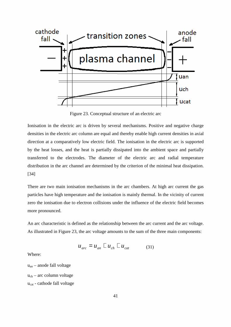
41
Figure 23. Conceptual structure of an electric arc
Ionisation in the electric arc is driven by several mechanisms. Positive and negative charge
densities in the electric arc column are equal and thereby enable high current densities in axial
direction at a comparatively low electric field. The ionisation in the electric arc is supported
by the heat losses, and the heat is partially dissipated into the ambient space and partially
transferred to the electrodes. The diameter of the electric arc and radial temperature
distribution in the arc channel are determined by the criterion of the minimal heat dissipation.
[34]
There are two main ionisation mechanisms in the arc chambers. At high arc current the gas
particles have high temperature and the ionisation is mainly thermal. In the vicinity of current
zero the ionisation due to electron collisions under the influence of the electric field becomes
more pronounced.
An arc characteristic is defined as the relationship between the arc current and the arc voltage.
As illustrated in Figure 23, the arc voltage amounts to the sum of the three main components:
catchanarc uuuu ++= (31)
Where:
uan – anode fall voltage
uch – arc column voltage
ucat - cathode fall voltage

42
The arc characteristic is a non-linear function, which depends on many factors such as
quenching medium type and its pressure, geometry of the contacts, nozzle and internal
arrangement of the quenching chamber. The electric arc exhibits the properties of thermal
inertia and for this reason static and dynamic arc characteristics should be differentiated. The
static arc characteristic describes the dependency of the arc voltage from the arc current in a
steady state, at constant arc length and cooling intensity. The assemblage of static arc
characteristics for different lengths and cooling intensities is descriptively illustrated in Figure
24.
Figure 24. The static arc characteristic
In the low-current range the arc behaviour reproduces the negative differential resistance,
where the arc voltage decreases with the increasing current. This property is explained by the
fact that at higher currents the diameter and temperature of the arc channel are higher, leading
to an increase in the arc conductivity [35]. For the rising part of the arc characteristic in the
high-current range there are several interpretations; among which are: the change in the arc
burning mechanism, increase of pressure in the closed volumes, arc confinement in nozzles
and slots, enlarging of the anode falls [36].
In the case of very fast arc current variations the arc voltage deviates from the curve of the
static characteristic. The arc column temperature and diameter cannot change instantaneously,
and the arc conductance correspondingly, owing to the thermal inertia of the arc. Therefore, at
stepwise increase of the current from I1 to I2, as shown in Figure 25a, the operating point
jumps from 1 to 1’ and the voltage changes abruptly from U1 to U1’. Then the arc resistance
43
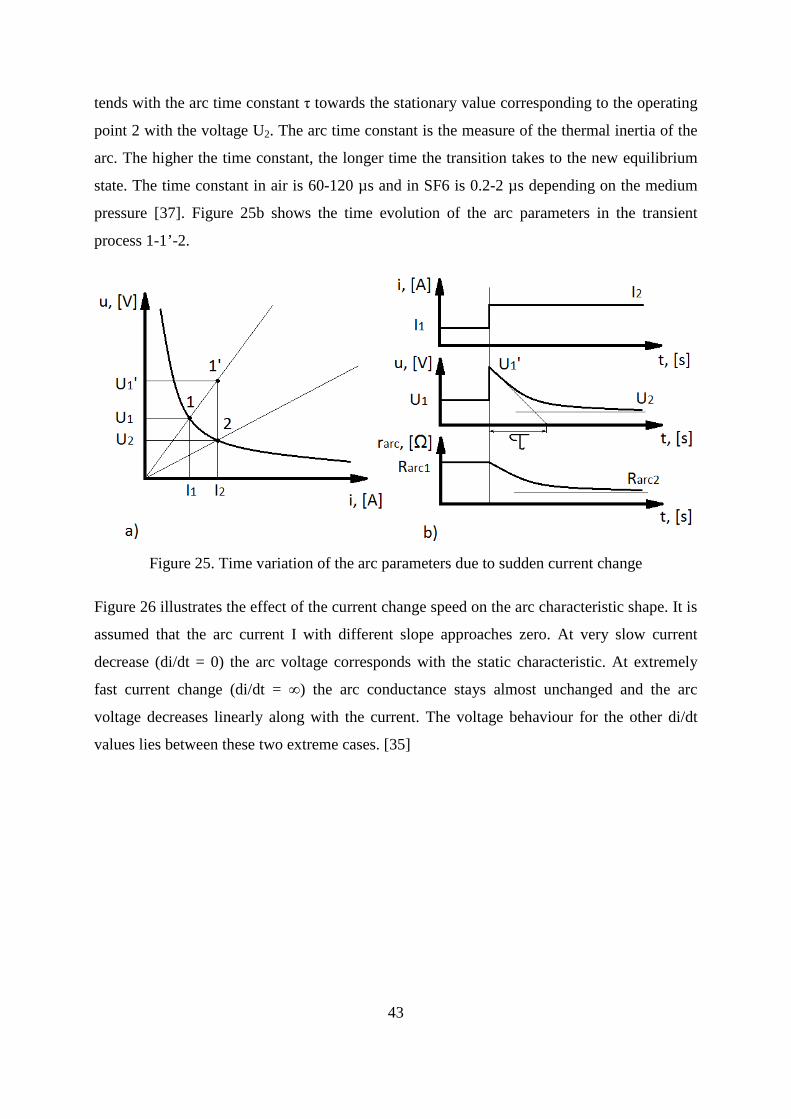
tends with the arc time constant τ towards the stationary value corresponding to the operating
point 2 with the voltage U2. The arc time constant is the measure of the thermal inertia of the
arc. The higher the time constant, the longer time the transition takes to the new equilibrium
state. The time constant in air is 60-120 µs and in SF6 is 0.2-2 µs depending on the medium
pressure [37]. Figure 25b shows the time evolution of the arc parameters in the transient
process 1-1’-2.
Figure 25. Time variation of the arc parameters due to sudden current change
Figure 26 illustrates the effect of the current change speed on the arc characteristic shape. It is
assumed that the arc current I with different slope approaches zero. At very slow current
decrease (di/dt = 0) the arc voltage corresponds with the static characteristic. At extremely
fast current change (di/dt = ∞) the arc conductance stays almost unchanged and the arc
voltage decreases linearly along with the current. The voltage behaviour for the other di/dt
values lies between these two extreme cases. [35]
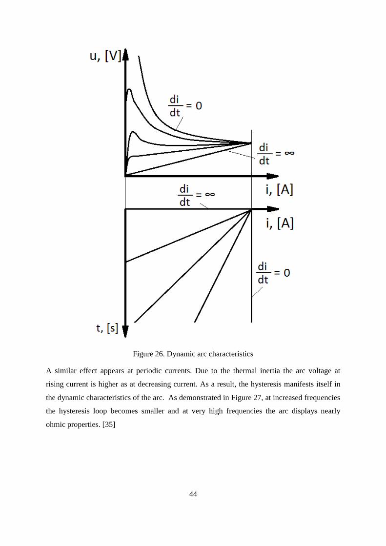
44
Figure 26. Dynamic arc characteristics
A similar effect appears at periodic currents. Due to the thermal inertia the arc voltage at
rising current is higher as at decreasing current. As a result, the hysteresis manifests itself in
the dynamic characteristics of the arc. As demonstrated in Figure 27, at increased frequencies
the hysteresis loop becomes smaller and at very high frequencies the arc displays nearly
ohmic properties. [35]

45
Figure 27. Arc characteristics and the arc voltage time curves at AC
Static and dynamic arc characteristics can be determined either experimentally or analytically
by solving the system of the descriptive magnetohydrodynamic equations. As a rule, in
theoretical studies the channel model of the arc and a series of assumptions and
simplifications are applied.
3.1.2 Arc extinction theory
The extinction of the electric arc always occurs at the current passage through zero. The arc
quenching itself can be understood as a transition of the arc resistance from initially low to
finally almost infinite value, which takes place during a very short time interval. Current zero
is only the prerequisite and not the sufficient condition of the arc extinction: after zero current
the arc may remain quenched or may reignite. The reasons of unsuccessful interruptions are
different by nature and relate to either thermal or dielectric breakdowns [38].
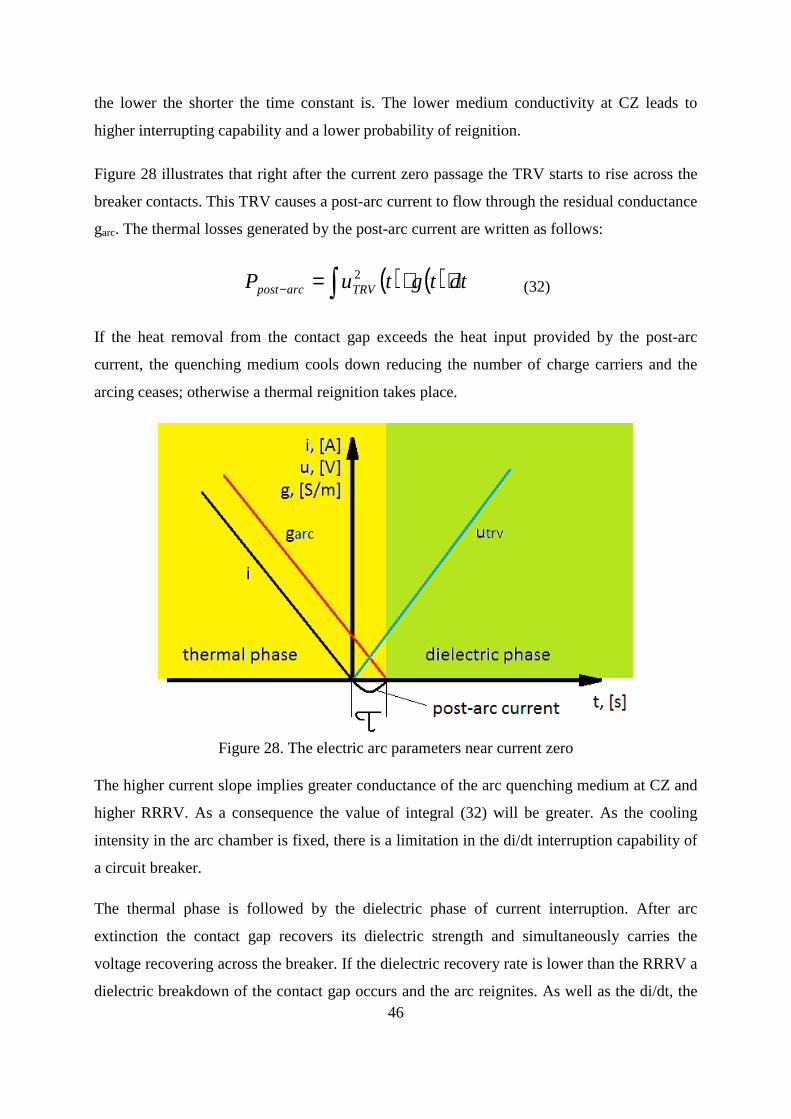
When the arc current becomes zero the quenching medium in the contact gap still has a finite
conductivity. This residual conductivity, which results from the thermal inertia of the arc, is
46
the lower the shorter the time constant is. The lower medium conductivity at CZ leads to
higher interrupting capability and a lower probability of reignition.
Figure 28 illustrates that right after the current zero passage the TRV starts to rise across the
breaker contacts. This TRV causes a post-arc current to flow through the residual conductance
garc. The thermal losses generated by the post-arc current are written as follows:
( ) ( ) dttgtuP TRVarcpost ∫ ⋅⋅=−2
(32)
If the heat removal from the contact gap exceeds the heat input provided by the post-arc
current, the quenching medium cools down reducing the number of charge carriers and the
arcing ceases; otherwise a thermal reignition takes place.
Figure 28. The electric arc parameters near current zero
The higher current slope implies greater conductance of the arc quenching medium at CZ and
higher RRRV. As a consequence the value of integral (32) will be greater. As the cooling
intensity in the arc chamber is fixed, there is a limitation in the di/dt interruption capability of
a circuit breaker.
The thermal phase is followed by the dielectric phase of current interruption. After arc
extinction the contact gap recovers its dielectric strength and simultaneously carries the
voltage recovering across the breaker. If the dielectric recovery rate is lower than the RRRV a
dielectric breakdown of the contact gap occurs and the arc reignites. As well as the di/dt, the
47
du/dt withstand capability is limited, too, and plays an important role especially when short-
line faults are concerned.
At sufficiently prolonged time after arc extinction the peak value of the recovery voltage may
outreach the withstand voltage of the fully recovered dielectric. The breakdown occurring in
this case is defined as a restrike. However, the peak value of the recovery voltage can be
limited with the use of overvoltage suppressors. Therefore, the most critical parameters
describing the mechanical breaker performance in the thermal and dielectric phases are di/dt-
breaking and du/dt-withstand capabilities.
3.1.3 Arc-models overview
There are quite a number of different arc models created over a long period of switchgear
development. Describing the same phenomenon these models may vary in many aspects.
Some of the models describe the arcing process only as applied to a particular model of a
circuit breaker [39]; some of them can be applied to different circuit breakers, provided that
the descriptive parameters are fitted for each individual breaker [40], [41]. The other
distinction between different models can be made based on the range of currents. Certain of
the models are primarily intended for studies of the quenching capability of the circuit breaker
and precisely reproduce the arc behaviour in the vicinity of CZ [42]. The other models are
good in describing the high-current arc properties and useful when the breaker influence on
the network is studied [43]. Therefore, selecting the appropriate arc model is not a
straightforward task and depends on the research goal. The sections below review two basic
and one combined approaches towards the arc modelling.
3.1.3.1 Physical models
The physical models are based on the system of mutually complementary equations, which
describe different internal processes proceeding in the arc on the molecular level. Despite that
the models differ from one another in the initial premises applied to the arc, all of them rely
on the constitutive equation of heat balance:
accleakconvcondradformarc PPPPPPP +++++= (33)
Where:
Parc – total heat dissipation of the arc
48
Pform – heat consumed for the formation of new charge carriers
Prad – radiative heat dissipation
Pcond – conductive heat dissipation
Pconv – convective heat dissipation
Pleak – heat removal due to leaking charge carriers
Pacc – heat accumulation by the plasma
The other equations complete the system and serve to calculate the values of the components
being a part of the energy balance. These equations are:
• Poisson’s equation for the relationship between the electric field strength and the
electric potential
• Equation of continuity
• Expression for the electrons flow density
• Expression for the ions flow density
• Saha-Langmuir ionisation equation
The input parameters to the model are the initial and boundary conditions, the values of the
temperature-dependent parameters, gas temperature and flow velocity. The output parameters
are the arc temperature field, the cross-section and the arc resistance, which is determined
from the total heat dissipation:
2arc
arcarc i
PR = (34)
The aforementioned system of equations describes mainly the state of quasi-neutral plasma in
the arc column. In order to get precise voltage between the electrodes the model of the arc
channel has to be supplemented with the models considering the processes in the anode and in
the cathode fall zones.
49
The use of physical models is associated with the necessity to solve the system of differential
equations with non-constant coefficients. Furthermore, the data on the physical properties of
the arc quenching medium in a wide temperature range must be available. These requirements
make physical modelling time and resource consuming. Therefore, physical models can be
applied when the design of the internal design of the arc quenching chamber is in the focus,
whereas they are expected to be redundant when the breaker-network interaction is under
study.
3.1.3.2 “Black-box” models
A “black-box” model is a model that requires from the user no knowledge on the underlying
physical processes occurring in the modelled object. As applied to circuit breakers, a “black-
box” model contains only a mathematical description of the interaction of the electric arc and
the electric circuit; therefore, these models are also often referred to as the mathematical
models. The black-box model as a whole represents the temporal interdependence between
the arc conductance, the arc current and the arc voltage.
The point of departure for the most mathematical models is the energy balance of the electric
arc. The input heat energy must be equal to the sum of the accumulated and dissipated heat at
any instant of time, and the equation of the energy balance of the electric arc is written as:
dt
dQPiu arcarcarc +=⋅ (35)
Where:
Q – heat accumulated in the arc
The arc conductance is a function of the arc heat content:
( )Qfu
iG
arc
arcarc == (36)
The time variation of the arc conductance is obtained by differentiation of the equation (35):
( ) ( )( ) ( ) ( ) ( )arcarcarcarc PiuQf
dt
tdQ
dQ
tQdf
dt
tdG−⋅⋅′=⋅= (37)
50
Dividing (37) by the arc conductance gives:
( )( )
( )( )( ) ( ) ( )
( ) ( )arcarcarcarc
arc
PiuQf
Qf
dt
tdQ
dQ
tQdf
Qfdt
tdG
tG−⋅⋅
′=⋅⋅=⋅ 11
(38)
The practical use of the equation (38) requires the availability of the relations G = f(Q) and
Parc = f(iarc). This fact makes the arc model in the form (38) impractical. In order to find the
solutions of the equation (38) a set of assumptions should be introduced. The most known
approaches in this respect have been formulated by Cassie and Mayr.
The assumptions made by Cassie are best suited for the high-current region. Specific arc
resistance ρ, energy content per unit of arc volume c and energy dissipation per unit arc of
volume λ are assumed to be constant. The cross-section of the arc A, by contrast, is regarded
as variable. Per unit of the arc length the following notation is valid:
( )ρρ ⋅
====c
QAQf
u
iG
arc
arcarc (39)
The dissipated heat per unit of the arc length is defined as:
λλ ⋅=⋅=c
QAParc (40)
Substitution of (39) and (40) into (38) gives:
( )( )
−
⋅=⋅ 1
112
0U
u
dt
tdG
tGarc
c
arc
arc τ (39)
Where:
τc = c / λ – time constant of the arc according to Cassie
U0 = (λ · ρ)0.5 – arc voltage at high currents
In the Mayr’s hypothesis, which is quite true for the low-current range, the arc cross-section A
and the heat removal from the arc P = P0 are defined as constants. The heat content Q is a
function of the variable arc temperature. Mayr suggests the following relationship between the
arc conductivity and the energy content:

51
( ) 00
Q
Q
arc eGQfG ⋅== (40)
Expression (40) with constant parameters G0 and Q0 being substituted into (38) yields:
( )( )
−
⋅⋅=⋅ 1
11
0P
iu
dt
tdG
tGarcarc
m
arc
arc τ (41)
Where:
τm = Q0 / P0 - time constant of the arc according to Mayr
Under real conditions the parameters defining the time constant are not fixed but current
dependent. Therefore, it should be pointed out that in practice the time constant has no fixed
value in the whole current range, although the real arc can still be described by the same
differential equations.
The arc parameters are determined separately for each circuit breaker type by means of the
current-voltage characteristics produced during the laboratory tests. In order to get the
parameter values, the measured arc characteristics are compared with the model-output data.
There are also several other arc models that are structurally analogous to those of Cassie and
Mayr. Those models may offer more a precise approach towards the arc parameters
calculation, account for stochastic properties of a circuit breaker, etc.
3.1.4 SF6-breaker model development
The arc model should be easy and practical, in this way the balance between the arc model
complexity and the network complexity can be kept. In this study the „black-box“ approach
was used because it is more simple and it is better suited for the used simulation software. The
arc model is also required to be enough extensive in order to describe the following
characteristics:
• High-current arc - for analysis of the breaker-network interaction
• Low-current arc - for analysis of the breaking capability under DC conditions
• Dielectric recovery - for study of the breaker capability to withstand the network
reaction on the switching operations
52
Among the variety of the mathematical arc models [34], the arc model equation in the
modified form suggested by Habedank was given a priority [44]. The terms in the parentheses
in the equation (42) account for thermal and dielectric phenomena in the arc respectively. The
thermal part is responsible for the quenching capability and the dielectric part for the
capability to withstand TRV. The term iarc·U0 describes the constant part of the arc
characteristic at high currents.
( ) ( )
⋅⋅+
⋅+⋅=⋅+
2
20
00
211
D
arc
Darc
arcarc
arc
U
u
U
pf
Uip
itG
dt
tdG
ττ (42)
Where:
f – correcting factor defining the break-down voltage after the current interruption
UD – no-load break-down voltage
Based initially on the Schwarz’s theory, who considered power dissipation p0 and the time
constant τ as the functions dependent from the arc conductance [45], Wild et al. suggested to
determine the arc parameters according to the expressions below: [46]
βarcGppp ⋅+= 210 (43)
ατττ arcG⋅+= 21 (44)
Where:
p1, p2, τ1, τ2, α, β - constants
Determination of the arc parameters in the present work depends on the arcing phase. In the
arc firing phase, namely in the range of currents above 50A, the heat removal p0 is calculated
according to the expression (43). In the arc quenching phase, i.e. at currents below 50A, the
heat removal p0 is not dependent on the arc conductance [47] and assumed to be constant.
Expression (44) is used for calculation of the time constant in the both arcing phases.
In order to determine the arc parameters in the firing phase, the arc characteristic produced by
the results of test measurements done in KEMA high-voltage laboratory was taken as a
reference. This dynamic arc characteristic corresponding to a 50 Hz arc current is shown in
Figure 29.

53
Figure 29. Arc characteristic for one AP-interrupter unit
In terms of mechanics, operation of a real circuit breaker is not instantaneous. The operating
mechanism needs certain time to accelerate the moving contact and the flow of SF6 through
the nozzle develops with a time delay, too. The effect of changing conditions in the arc
chamber during breaker tripping can be taken into account by introducing a correction factor e
for the arc voltage:
( ) ( ) ( )tetutu arcrarc ⋅= (45)
Figure 30 illustrates a manner in which the heat removal from the arc varies during current
breaking. This dependency of the voltage across the contacts from the arcing time was
implemented in the circuit breaker model.
Figure 30. Time dependence of the correction factor e [48]
54
With reference to Figure 30, it takes around 10 ms for the modern circuit breaker to separate
the contacts enough to withstand voltage after interruption of large current. After 10 ms the
breaker develops the full arc voltage, when the movable contacts reach their full breaking
distance and the maximum SF6 flow through the nozzle is established. Arcing at highest
voltage lasts nearly 15 ms and then SF6 flow gradually ceases and the arc voltage decreases.
Decreasing cooling of the arc reduces breaking capability and necessitates arc quenching
within 25ms after tripping.
3.1.5 Parameter determination and validation of the model
After selecting the proper model equation and estimation of the model parameters the model
has to be verified. Verification means a proof whether the implemented model reproduces the
real phenomenon with sufficient exactness or not.
As said in the previous section, the arc parameters describing thermal properties are
determined depending on the arcing phase.
• Arc firing phase
The parameter values for the firing phase are supposed to be derived by fitting the model
output arc characteristic with the experimentally measured one. However, the characteristic in
Figure 29 is taken for a 145 kV P-type interrupter. For modelling of the 250 kV T-type
interrupter unit, the arcing voltage is assumed to be two times higher than that in Figure 29 for
each respective current. The thus obtained reference characteristic is used subsequently for
validation of the model performance at high currents. The arc parameters for the arc firing
phase are:
35.0330 1080010150 arcGp ⋅⋅+⋅= [W]
15.066 1022.01022.0 arcG⋅⋅+⋅= −−τ [s]
Comparison of the real and simulated characteristics shows a good agreement as
demonstrated in Figure 31.
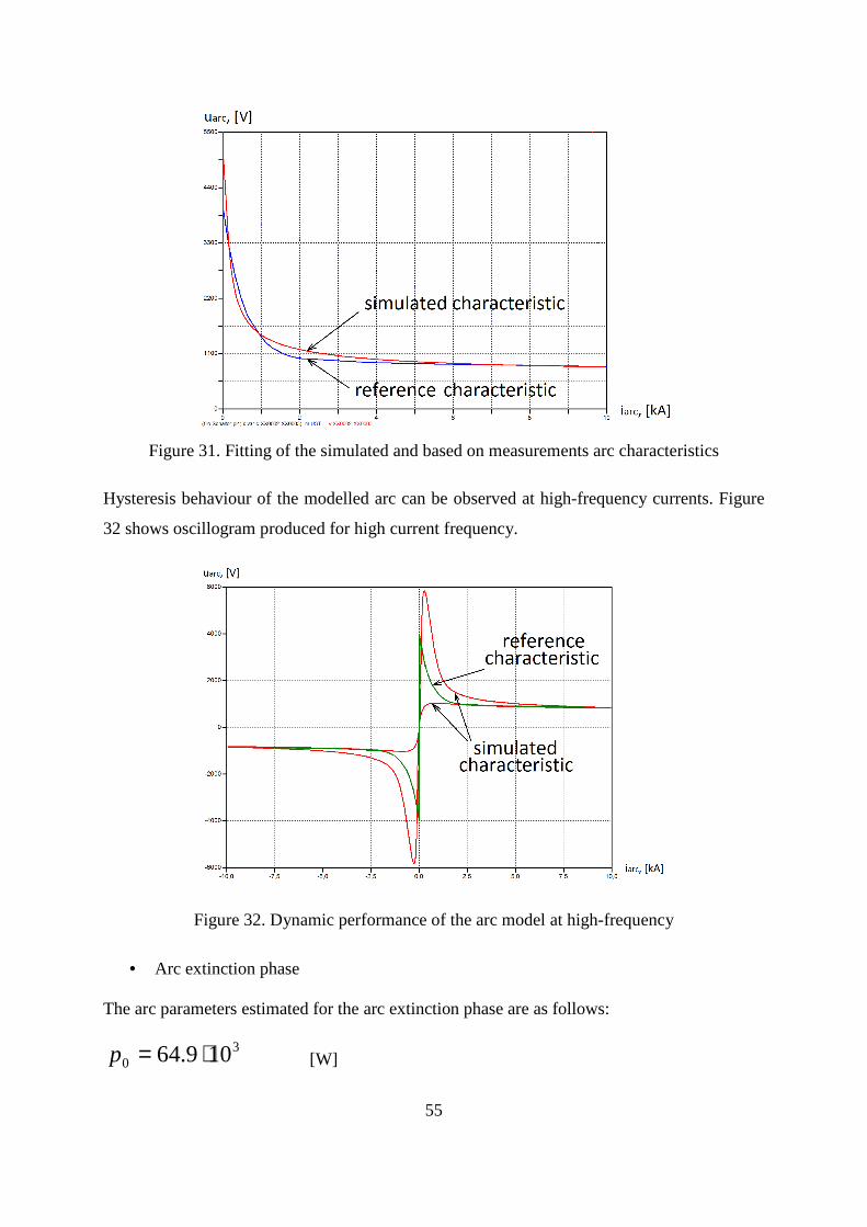
55
Figure 31. Fitting of the simulated and based on measurements arc characteristics
Hysteresis behaviour of the modelled arc can be observed at high-frequency currents. Figure
32 shows oscillogram produced for high current frequency.
Figure 32. Dynamic performance of the arc model at high-frequency
• Arc extinction phase The arc parameters estimated for the arc extinction phase are as follows:
30 109.64 ⋅=p [W]

56
15.066 1022.01022.0 arcG⋅⋅+⋅= −−τ [s]
Cooling intensity p0 = 64.9 kW is chosen to provide the declared short-circuit breaking
capability (50 kA RMS) of the 250 kV “AT”-interrupter of Siemens.
For the currents higher than 11.3 kA, which are not covered by the available arc
characteristic, the characteristic curve tendency is assumed to be horizontal. Based on this
assumption, the voltage influencing the constant part of the arc characteristic at high currents
U0 = 625 V is specified.
For the dielectric part of the arc characteristic (42) the integrated parameter was determined:
1540 10625 −⋅=⋅=DU
pfF [S/V2]
The value of the integrated parameter F is determined by means of iterations, proceeding from
the universally accepted capability of an SF6 circuit breaker to withstand a RRRV, which is
assumed to be 15 kV/µs.
3.2 Vacuum breaker modelling
For already more than five decades of being in service vacuum circuit breakers proved to be a
successful technology for protection of the AC networks. It is a peculiarity of vacuum circuit
breakers that they possess the capability of very fast dielectric recovery after current zero at
comparatively small contact gaps. Figure 33 makes this fact obvious showing the course of
dielectric recovery after current zero (Irms = 1600 A, contact gap 6 mm).
Figure 33. Dielectric recovery after current zero in vacuum and SF6 over time [49]
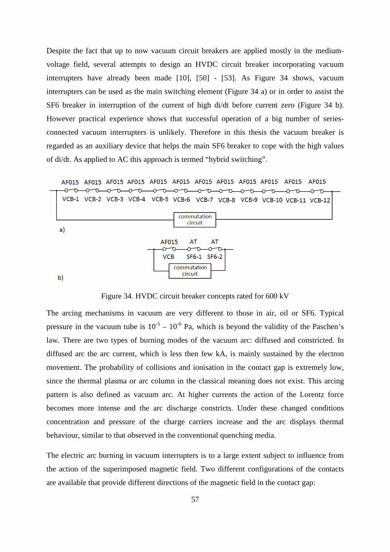
57
Despite the fact that up to now vacuum circuit breakers are applied mostly in the medium-
voltage field, several attempts to design an HVDC circuit breaker incorporating vacuum
interrupters have already been made [10], [50] - [53]. As Figure 34 shows, vacuum
interrupters can be used as the main switching element (Figure 34 a) or in order to assist the
SF6 breaker in interruption of the current of high di/dt before current zero (Figure 34 b).
However practical experience shows that successful operation of a big number of series-
connected vacuum interrupters is unlikely. Therefore in this thesis the vacuum breaker is
regarded as an auxiliary device that helps the main SF6 breaker to cope with the high values
of di/dt. As applied to AC this approach is termed “hybrid switching”.
Figure 34. HVDC circuit breaker concepts rated for 600 kV
The arcing mechanisms in vacuum are very different to those in air, oil or SF6. Typical
pressure in the vacuum tube is 10-5 – 10-6 Pa, which is beyond the validity of the Paschen’s
law. There are two types of burning modes of the vacuum arc: diffused and constricted. In
diffused arc the arc current, which is less then few kA, is mainly sustained by the electron
movement. The probability of collisions and ionisation in the contact gap is extremely low,
since the thermal plasma or arc column in the classical meaning does not exist. This arcing
pattern is also defined as vacuum arc. At higher currents the action of the Lorentz force
becomes more intense and the arc discharge constricts. Under these changed conditions
concentration and pressure of the charge carriers increase and the arc displays thermal
behaviour, similar to that observed in the conventional quenching media.
The electric arc burning in vacuum interrupters is to a large extent subject to influence from
the action of the superimposed magnetic field. Two different configurations of the contacts
are available that provide different directions of the magnetic field in the contact gap:
58
• Contacts inducing axial magnetic field that prevents vacuum arc from constriction at
high currents, thereby preventing local overheat of the contact surface
• Contacts inducing radial magnetic field that forces the constricted arc column to rotate
at the contact surface in order to increase the arc voltage
A vacuum arc is more difficult to predict and more difficult to fully understand its nature. The
arc models of Cassie and Mayr are not applicable to vacuum breakers and there are no other
“black box” models developed. The vacuum arc has been experimentally investigated for
many years and few attempts to model the dynamics of vacuum arc have been undertaken
[54], [55]. However, these reported models can hardly be regarded as universal for various
study cases, because they represent only mathematical approximations of the experimentally
measured curves under specified test conditions. Therefore, in the present study a simplified
approach to the vacuum breaker modelling was taken.
Medium-voltage vacuum circuit breaker was found suitable for using as a part HVDC circuit
breakers. The type chosen has following ratings: rated RMS voltage of 36 kV, rated normal
current 2 kA, rated short-circuit breaking current 31,5 kA. A breaker was modelled as an ideal
switch, which opens at current zero if di/dt was less than its breaking capability. The ideal
switch representing the VCB may close if after the interruption the RRRV exceeds the rate of
recovery of the dielectric strength. This modelling approach is justified by the fact that at high
currents the vacuum breaker arc voltage is below 150 V, which is sufficiently low to influence
the network. In [51] the performance of vacuum interrupter as a component of an HVDC CB
with determined breaking capability di/dt = 500 A/µs and voltage withstand capability RRRV
= 50 kV/µs was declared.
59
3.3 Modelling of semiconductor switches
When it comes to simulation studies of solid-state or hybrid HVDC circuit breakers, the fully
controllable semiconductor switches are of interest. These fully controllable devices can be
represented by power transistors or power thyristors possessing switching off capability. The
present work does not focus on the physical processes in the semiconductor switches but aims
at investigation of influence on the circuit of a switching operation performed by a fully
controllable switch. Additionally, the possible consequences of the network transients for the
power electronics elements will be analysed.
The simplified approach to modelling of the semiconductor switches similar to reported in
[31] is taken. A stack of semiconductor modules connected in series to meet the required
system voltage is represented by a single switch regardless of the number of modules. No
parasitic reactances of the actual connections and joints and no input, output or internal switch
capacitances are taken into account. The element representing the IGBT-based switch has
zero resistance in conduction mode and linearly increasing resistance from 0 to 1 MΩ within
200 µs at switching off.
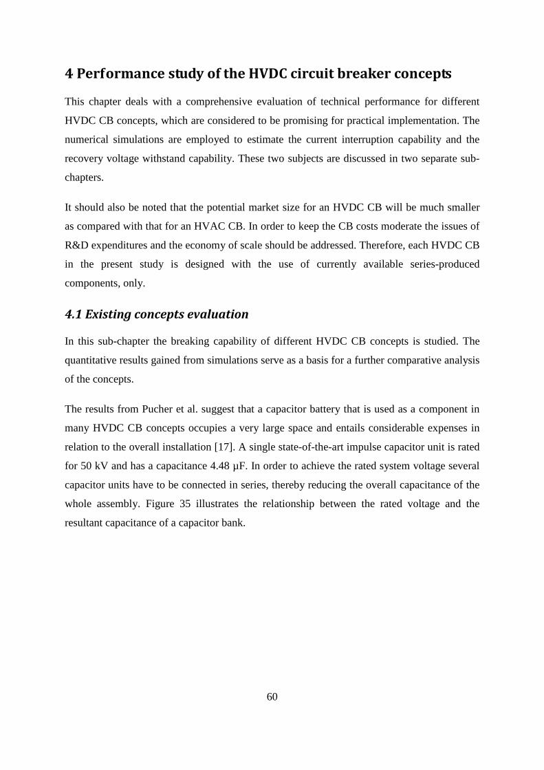
60
4 Performance study of the HVDC circuit breaker concepts
This chapter deals with a comprehensive evaluation of technical performance for different
HVDC CB concepts, which are considered to be promising for practical implementation. The
numerical simulations are employed to estimate the current interruption capability and the
recovery voltage withstand capability. These two subjects are discussed in two separate sub-
chapters.
It should also be noted that the potential market size for an HVDC CB will be much smaller
as compared with that for an HVAC CB. In order to keep the CB costs moderate the issues of
R&D expenditures and the economy of scale should be addressed. Therefore, each HVDC CB
in the present study is designed with the use of currently available series-produced
components, only.
4.1 Existing concepts evaluation
In this sub-chapter the breaking capability of different HVDC CB concepts is studied. The
quantitative results gained from simulations serve as a basis for a further comparative analysis
of the concepts.
The results from Pucher et al. suggest that a capacitor battery that is used as a component in
many HVDC CB concepts occupies a very large space and entails considerable expenses in
relation to the overall installation [17]. A single state-of-the-art impulse capacitor unit is rated
for 50 kV and has a capacitance 4.48 µF. In order to achieve the rated system voltage several
capacitor units have to be connected in series, thereby reducing the overall capacitance of the
whole assembly. Figure 35 illustrates the relationship between the rated voltage and the
resultant capacitance of a capacitor bank.
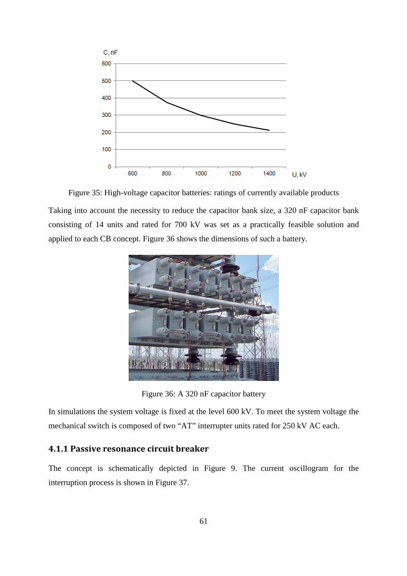
61
Figure 35: High-voltage capacitor batteries: ratings of currently available products
Taking into account the necessity to reduce the capacitor bank size, a 320 nF capacitor bank
consisting of 14 units and rated for 700 kV was set as a practically feasible solution and
applied to each CB concept. Figure 36 shows the dimensions of such a battery.
Figure 36: A 320 nF capacitor battery
In simulations the system voltage is fixed at the level 600 kV. To meet the system voltage the
mechanical switch is composed of two “AT” interrupter units rated for 250 kV AC each.
4.1.1 Passive resonance circuit breaker
The concept is schematically depicted in Figure 9. The current oscillogram for the
interruption process is shown in Figure 37.

62
Figure 37: Current oscillations in a breaking process of a passive HVDC CB
The operating principle of this circuit breaker resembles the current chopping
phenomenon. At current chopping the same current oscillating behaviour is observed
when the current of fundamental frequency approaches zero. The current voltage diagram
of the oscillation process is given below in Figure 38.
Figure 38: Trajectory of the arc current-voltage oscillations during switching
Due to the limitations on the capacitor size and on the inductor size consequently, the current
oscillations have frequencies of the order of several kHz. The current oscillations generated
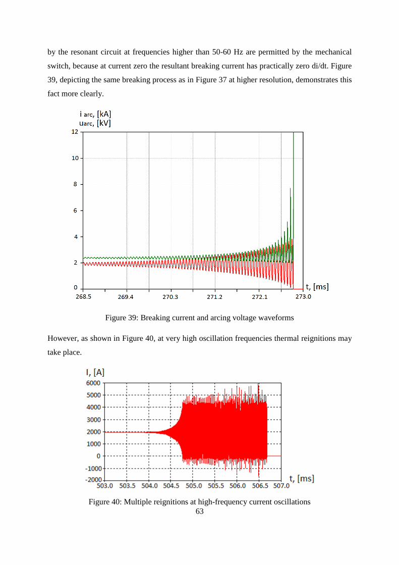
63
by the resonant circuit at frequencies higher than 50-60 Hz are permitted by the mechanical
switch, because at current zero the resultant breaking current has practically zero di/dt. Figure
39, depicting the same breaking process as in Figure 37 at higher resolution, demonstrates this
fact more clearly.
Figure 39: Breaking current and arcing voltage waveforms
However, as shown in Figure 40, at very high oscillation frequencies thermal reignitions may
take place.
Figure 40: Multiple reignitions at high-frequency current oscillations
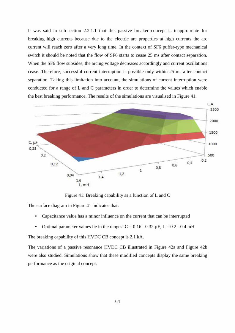
64
It was said in sub-section 2.2.1.1 that this passive breaker concept is inappropriate for
breaking high currents because due to the electric arc properties at high currents the arc
current will reach zero after a very long time. In the context of SF6 puffer-type mechanical
switch it should be noted that the flow of SF6 starts to cease 25 ms after contact separation.
When the SF6 flow subsides, the arcing voltage decreases accordingly and current oscillations
cease. Therefore, successful current interruption is possible only within 25 ms after contact
separation. Taking this limitation into account, the simulations of current interruption were
conducted for a range of L and C parameters in order to determine the values which enable
the best breaking performance. The results of the simulations are visualised in Figure 41.
Figure 41: Breaking capability as a function of L and C
The surface diagram in Figure 41 indicates that:
• Capacitance value has a minor influence on the current that can be interrupted
• Optimal parameter values lie in the ranges: C = 0.16 - 0.32 µF, L = 0.2 - 0.4 mH
The breaking capability of this HVDC CB concept is 2.1 kA.
The variations of a passive resonance HVDC CB illustrated in Figure 42a and Figure 42b
were also studied. Simulations show that these modified concepts display the same breaking
performance as the original concept.
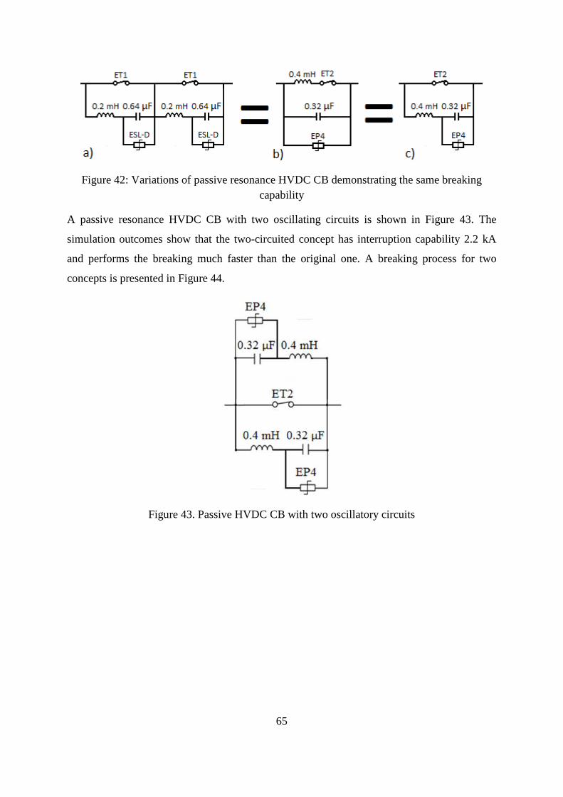
65
Figure 42: Variations of passive resonance HVDC CB demonstrating the same breaking capability
A passive resonance HVDC CB with two oscillating circuits is shown in Figure 43. The
simulation outcomes show that the two-circuited concept has interruption capability 2.2 kA
and performs the breaking much faster than the original one. A breaking process for two
concepts is presented in Figure 44.
Figure 43. Passive HVDC CB with two oscillatory circuits
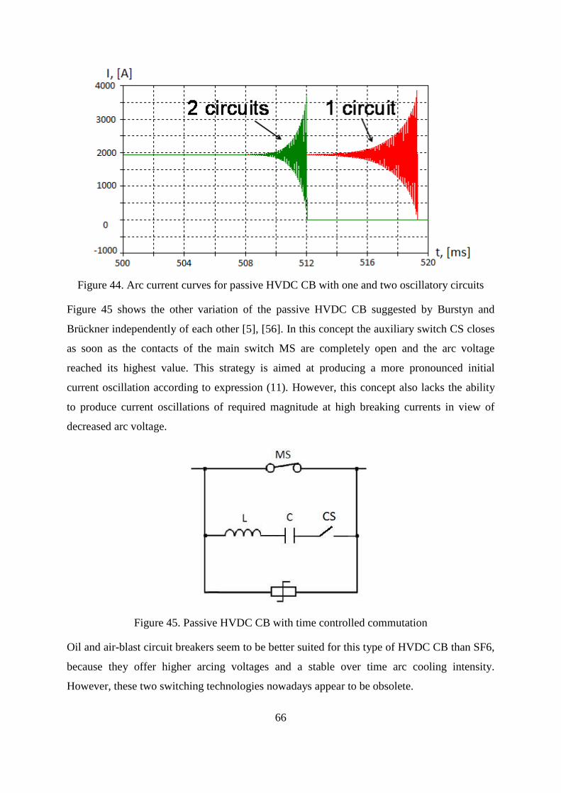
66
Figure 44. Arc current curves for passive HVDC CB with one and two oscillatory circuits
Figure 45 shows the other variation of the passive HVDC CB suggested by Burstyn and
Brückner independently of each other [5], [56]. In this concept the auxiliary switch CS closes
as soon as the contacts of the main switch MS are completely open and the arc voltage
reached its highest value. This strategy is aimed at producing a more pronounced initial
current oscillation according to expression (11). However, this concept also lacks the ability
to produce current oscillations of required magnitude at high breaking currents in view of
decreased arc voltage.
Figure 45. Passive HVDC CB with time controlled commutation
Oil and air-blast circuit breakers seem to be better suited for this type of HVDC CB than SF6,
because they offer higher arcing voltages and a stable over time arc cooling intensity.
However, these two switching technologies nowadays appear to be obsolete.

67
4.1.2 Active resonance circuit breaker
As opposed to a self-excited resonance HVDC CB, a pre-charged oscillating circuit of the
active HVDC CB (Figure 10) provides stronger current impulses for creation of current zero,
making this CB applicable for breaking higher DC currents. In Figure 46 the red line shows
current impulses superimposed on the breaking DC current and the green line shows the
mechanical switch current for the case of successful current interruption at current zero.
Figure 46. Current through the mechanical switch of an active HVDC CB
The characteristic impedance of the oscillating circuit (L/C)0.5 determines the current
oscillation amplitude according to expression (13). After interruption the commutation
capacitor has to withstand the full system voltage, therefore several capacitor units must be
connected in series. The resultant capacitance of the bank is assumed to be 320 nF according
to Figure 35 at 700 kV. Thus, inductance variation is the only way to adjust the magnitude of
the current impulse. A smaller inductance provides current impulses with greater amplitude
and at the same time of higher frequency. Exceeding the limiting frequency value leads to
reignitions similar to those presented in Figure 40 due to increased di/dt value before current
zero.
Reignitions may also take place at breaking relatively low currents. If the breaking current
value is similar to that of the current impulse, the current through the mechanical switch
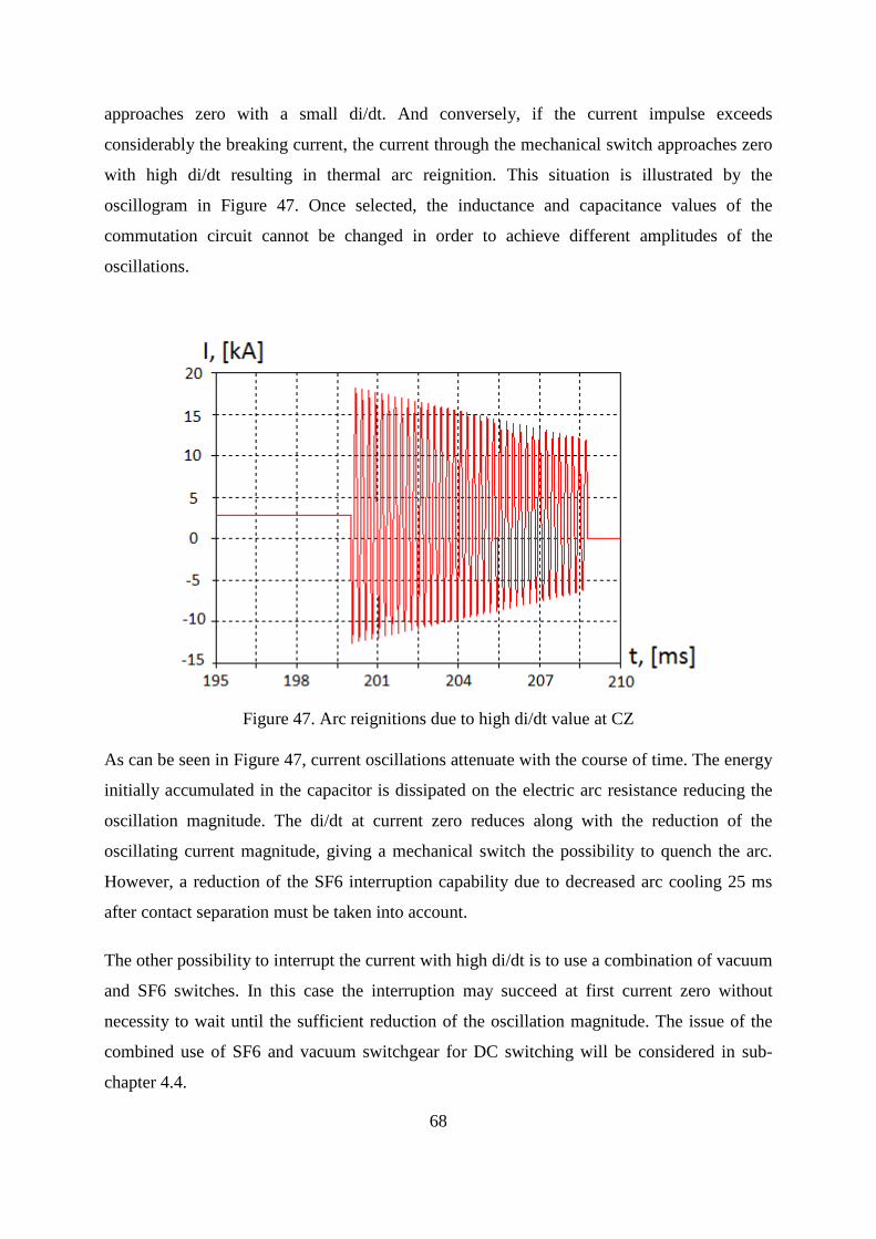
68
approaches zero with a small di/dt. And conversely, if the current impulse exceeds
considerably the breaking current, the current through the mechanical switch approaches zero
with high di/dt resulting in thermal arc reignition. This situation is illustrated by the
oscillogram in Figure 47. Once selected, the inductance and capacitance values of the
commutation circuit cannot be changed in order to achieve different amplitudes of the
oscillations.
Figure 47. Arc reignitions due to high di/dt value at CZ
As can be seen in Figure 47, current oscillations attenuate with the course of time. The energy
initially accumulated in the capacitor is dissipated on the electric arc resistance reducing the
oscillation magnitude. The di/dt at current zero reduces along with the reduction of the
oscillating current magnitude, giving a mechanical switch the possibility to quench the arc.
However, a reduction of the SF6 interruption capability due to decreased arc cooling 25 ms
after contact separation must be taken into account.
The other possibility to interrupt the current with high di/dt is to use a combination of vacuum
and SF6 switches. In this case the interruption may succeed at first current zero without
necessity to wait until the sufficient reduction of the oscillation magnitude. The issue of the
combined use of SF6 and vacuum switchgear for DC switching will be considered in sub-
chapter 4.4.

69
A set of simulations showed that an active HVDC CB with C = 320 nF and L = 1.2 mH has
the best interruption performance. Its interruption capability is 12 kA. The breaking time is
limited to 25 ms because after that the breaking capability of SF6 switch reduces and multiple
reignitions of the high-frequency arc take place.
4.1.3 Forced oscillation DC circuit breaker
The general outline of the HVDC CB operating on the forced oscillations principle is
presented in Figure 13. The main question regarding this breaker topology is what voltage
source should be employed. The voltage source can be implemented as demonstrated in
Figure 48.
Figure 48. HVDC CB with oscillating circuit powered by transistor bridge
The transistor pairs 1 - 4 and 2 - 3 switch on and off alternately providing the transformer
current frequency equal to the resonant frequency of the oscillatory circuit across the
mechanical switch. Figure 49 shows the current oscillogram for the current through the
mechanical switch in a breaking process.
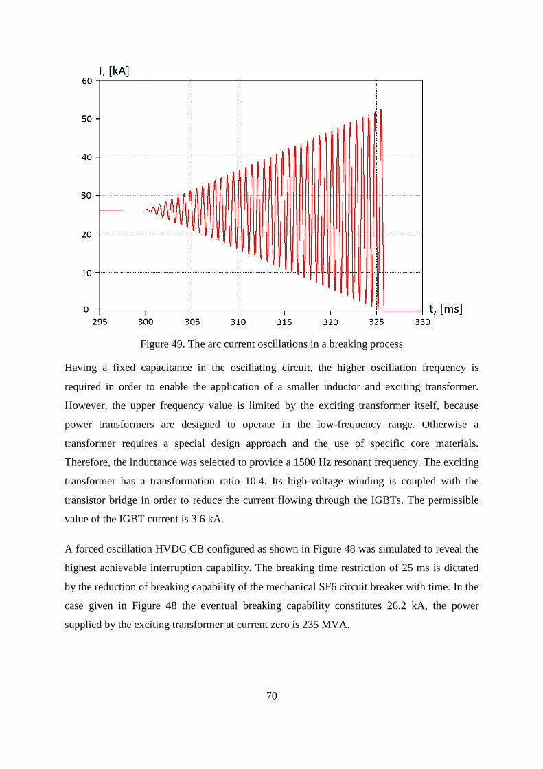
70
Figure 49. The arc current oscillations in a breaking process
Having a fixed capacitance in the oscillating circuit, the higher oscillation frequency is
required in order to enable the application of a smaller inductor and exciting transformer.
However, the upper frequency value is limited by the exciting transformer itself, because
power transformers are designed to operate in the low-frequency range. Otherwise a
transformer requires a special design approach and the use of specific core materials.
Therefore, the inductance was selected to provide a 1500 Hz resonant frequency. The exciting
transformer has a transformation ratio 10.4. Its high-voltage winding is coupled with the
transistor bridge in order to reduce the current flowing through the IGBTs. The permissible
value of the IGBT current is 3.6 kA.
A forced oscillation HVDC CB configured as shown in Figure 48 was simulated to reveal the
highest achievable interruption capability. The breaking time restriction of 25 ms is dictated
by the reduction of breaking capability of the mechanical SF6 circuit breaker with time. In the
case given in Figure 48 the eventual breaking capability constitutes 26.2 kA, the power
supplied by the exciting transformer at current zero is 235 MVA.
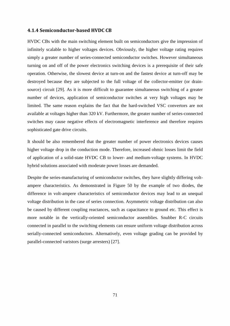
71
4.1.4 Semiconductor-based HVDC CB
HVDC CBs with the main switching element built on semiconductors give the impression of
infinitely scalable to higher voltages devices. Obviously, the higher voltage rating requires
simply a greater number of series-connected semiconductor switches. However simultaneous
turning on and off of the power electronics switching devices is a prerequisite of their safe
operation. Otherwise, the slowest device at turn-on and the fastest device at turn-off may be
destroyed because they are subjected to the full voltage of the collector-emitter (or drain-
source) circuit [29]. As it is more difficult to guarantee simultaneous switching of a greater
number of devices, application of semiconductor switches at very high voltages may be
limited. The same reason explains the fact that the hard-switched VSC convertors are not
available at voltages higher than 320 kV. Furthermore, the greater number of series-connected
switches may cause negative effects of electromagnetic interference and therefore requires
sophisticated gate drive circuits.
It should be also remembered that the greater number of power electronics devices causes
higher voltage drop in the conduction mode. Therefore, increased ohmic losses limit the field
of application of a solid-state HVDC CB to lower- and medium-voltage systems. In HVDC
hybrid solutions associated with moderate power losses are demanded.
Despite the series-manufacturing of semiconductor switches, they have slightly differing volt-
ampere characteristics. As demonstrated in Figure 50 by the example of two diodes, the
difference in volt-ampere characteristics of semiconductor devices may lead to an unequal
voltage distribution in the case of series connection. Asymmetric voltage distribution can also
be caused by different coupling reactances, such as capacitance to ground etc. This effect is
more notable in the vertically-oriented semiconductor assemblies. Snubber R-C circuits
connected in parallel to the switching elements can ensure uniform voltage distribution across
serially-connected semiconductors. Alternatively, even voltage grading can be provided by
parallel-connected varistors (surge arresters) [27].
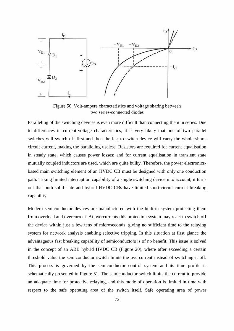
72
Figure 50. Volt-ampere characteristics and voltage sharing between two series-connected diodes
Paralleling of the switching devices is even more difficult than connecting them in series. Due
to differences in current-voltage characteristics, it is very likely that one of two parallel
switches will switch off first and then the last-to-switch device will carry the whole short-
circuit current, making the paralleling useless. Resistors are required for current equalisation
in steady state, which causes power losses; and for current equalisation in transient state
mutually coupled inductors are used, which are quite bulky. Therefore, the power electronics-
based main switching element of an HVDC CB must be designed with only one conduction
path. Taking limited interruption capability of a single switching device into account, it turns
out that both solid-state and hybrid HVDC CBs have limited short-circuit current breaking
capability.
Modern semiconductor devices are manufactured with the built-in system protecting them
from overload and overcurrent. At overcurrents this protection system may react to switch off
the device within just a few tens of microseconds, giving no sufficient time to the relaying
system for network analysis enabling selective tripping. In this situation at first glance the
advantageous fast breaking capability of semiconductors is of no benefit. This issue is solved
in the concept of an ABB hybrid HVDC CB (Figure 20), where after exceeding a certain
threshold value the semiconductor switch limits the overcurrent instead of switching it off.
This process is governed by the semiconductor control system and its time profile is
schematically presented in Figure 51. The semiconductor switch limits the current to provide
an adequate time for protective relaying, and this mode of operation is limited in time with
respect to the safe operating area of the switch itself. Safe operating area of power
73
semiconductor defines the area on the current-voltage plot in which the device can operate
without damage.
Figure 51. Proactive control of the ABB hybrid HVDC CB [20]
The design of the hybrid ABB HVDC CB is complicated by the cooling requirement.
Assuming the voltage drop across the commutation switch to be 1 V, which is quite a realistic
value, the heat losses constitute 2 kW at 2 kA load current. This high heat emission cannot be
handled by an air-cooled heat sink and it should be removed with the help of the active water
cooling system.
In contrast to the ABB concept, the hybrid concept depicted in Figure 21 has no cooling
requirement and needs two times less semiconductor devices because in normal operation the
current flows through mechanical switches. SF6 switches may be used in this hybrid concept,
which need to have the same voltage rating as the main semiconductor switch, because after
interruption they are connected in parallel and carry full system voltage.
In fact, there is not much to investigate about the current breaking capability of the
semiconductors, but the points of interest are the network reaction on the switching operation
and the consequences of this network reaction for the switch itself. The simulation results of
the DC current breaking by semiconductor-based devices are presented in the chapter
dedicated to TRV.
74
4.2 The selection criteria for semiconductor switches
As can be seen in Table 2, fully controllable devices such as GTO, IGCT and IGBT can be
used as switching elements in semiconductor-based HVDC CBs. The current tendency in the
world of power electronics is that IGCT will most probably completely substitute GTO,
because it has lower conduction losses and a higher du/dt withstand capability [28]. In
contrast to converter applications, for HVDC the switching frequency of these different
semiconductors is of no importance, because even the slowest device is fast enough for the
network protection. However, for a number of reasons listed below, IGBT can be regarded as
the most likely candidate for the switching element of an HVDC CB:
• There is no need for paralleling if the IGBT transistors are selected. The point is that
the switching-off capability of IGBTs is 5-10 times higher than their current carrying
capacity. Therefore, a single IGBT can conduct and switch off the short-circuit current
within its technical capabilities. The switch-off capability of modern IGBT devices is
limited to 9 kA, whereas it is expected that the next generation of IGBTs will show a
breaking performance of up to 16 kA [57].
• IGBT can be triggered optically, whereas IGCT requires a substantial current impulse
to perform the switch-off operation. Optical control is immune to electromagnetic
interference. Furthermore, the optical fibre cable can be much longer than the
current/voltage signal cable, because it has no voltage drop. A longer signal cable
means that the control device can be distantly located.
• IGBTs, as well as IGCTs and some other semiconductor devices, are implemented as
smart power modules incorporating snubber and control circuits in one device. This
approach reduces the overall price of the control-snubber-switch system and makes the
modules easy to connect with one another.
As regards the IGBT design, this transistor type can have two different structures as shown in
Figure 52. In contrast to a non-punch through design, a punch-through IGBT has an additional
highly-doped n+ layer between p+ and n- layers of the first junction, which is on the collector
side. Furthermore, the first n+ layer of the punch-through IGBT is thinner than that of the
non-punch through one. These differences in inner structures result in different electric field
distribution patterns of the switch and define the device features. Thus, for example, a punch-

75
through IGBT has reduced switching time. It also has a negative temperature coefficient,
which makes it unsuitable for making parallel IGBT connections, although, as discussed
earlier, this feature is not required for an IGBT-based HVDC CB. A reduced on-state voltage
drop is peculiar to non-punch through devices [29].
Figure 52. IGBT structures and their internal field profile
There are also two different housing technologies for IGBTs. The HiPak and StakPak devices
incorporating both IGBT and anti-parallel diode are demonstrated in Figure 53.
Figure 53. a) HiPak and b) StakPak housing technologies for IGBTs
StakPak IGBTs are designed especially for easy electrical and mechanical connection in
series and therefore are preferred for HVDC. In order to achieve higher reliability redundant
devices must be provided in the switching assembly. Should some of StakPak devices have

76
failed, the StakPak remains in the short-circuited state and guarantees uninterrupted operation
of the whole series assembly. [27]
4.3 Transient recovery voltage (TRV)
Besides the task to interrupt current, an HVDC CB must withstand the transient recovery
voltage after a successful breaking event. TRV is the electric potential difference that appears
across the circuit breaker terminals after interruption. At the source-connected terminal the
electric potential has oscillating character and is determined by the interaction of a voltage
source and a source-side part of the circuit, which can be represented as an RLC-equivalent.
At the load terminal of a circuit breaker the potential is determined by the network and a load.
Recovery voltage withstand concerns two aspects:
• CB capability to withstand the RRRV, du/dt in other words.
As explained in section 3.1.2, the RRRV withstand is the second phase of current interruption
by a mechanical switch. If the mechanical switch fails to withstand the RRRV a dielectric
reignition takes place. Untolerated by a semiconductor device du/dt leads to its destruction,
which is defined as secondary breakdown. Secondary breakdown is a consequence of local
overheating of p-n junctions in a semiconductor device due to non-uniform current density
caused by a high du/dt.
• CB capability to withstand the peak value of the recovery voltage.
A high peak value of the recovery voltage leads to restrike of the electric arc in mechanical
switchgear and to primary breakdown in power electronics devices. These both phenomena
are caused by an increased electric field induced by the recovery voltage applied to a device.
Among these two recovery-voltage issues, du/dt deserves greater attention and is discussed in
sections 4.3.1 and 4.3.2 separately for oscillation and a semiconductor-based HVDC CB. The
aspect of peak recovery voltage is treated in section 4.3.3.
In the context of network protection the short-line fault is the most severe switching case from
the point of view of TRV withstand. In the simulation part attention was paid only to
overhead line (OHL) switching, since it has a higher surge impedance than a cable line and
therefore causes higher RRRV.
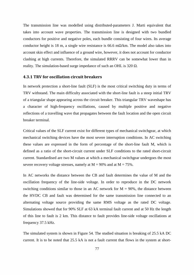
77
The transmission line was modelled using distributed-parameters J. Marti equivalent that
takes into account wave properties. The transmission line is designed with two bundled
conductors for positive and negative poles, each bundle consisting of four wires. Its average
conductor height is 18 m, a single wire resistance is 66.6 mΩ/km. The model also takes into
account skin effect and influence of a ground wire, however, it does not account for conductor
clashing at high currents. Therefore, the simulated RRRV can be somewhat lower than in
reality. The simulation-based surge impedance of such an OHL is 320 Ω.
4.3.1 TRV for oscillation circuit breakers
In network protection a short-line fault (SLF) is the most critical switching duty in terms of
TRV withstand. The main difficulty associated with the short-line fault is a steep initial TRV
of a triangular shape appearing across the circuit breaker. This triangular TRV waveshape has
a character of high-frequency oscillations, caused by multiple positive and negative
reflections of a travelling wave that propagates between the fault location and the open circuit
breaker terminal.
Critical values of the SLF current exist for different types of mechanical switchgear, at which
mechanical switching devices have the most severe interruption conditions. In AC switching
these values are expressed in the form of percentage of the short-line fault M, which is
defined as a ratio of the short-circuit current under SLF conditions to the rated short-circuit
current. Standardised are two M values at which a mechanical switchgear undergoes the most
severe recovery voltage stresses, namely at M = 90% and at M = 75%.
In AC networks the distance between the CB and fault determines the value of M and the
oscillation frequency of the line-side voltage. In order to reproduce in the DC network
switching conditions similar to those in an AC network for M = 90%, the distance between
the HVDC CB and fault was determined for the same transmission line connected to an
alternating voltage source providing the same RMS voltage as the rated DC voltage.
Simulations showed that for 90% SLF at 63 kA terminal fault current and at 50 Hz the length
of this line to fault is 2 km. This distance to fault provides line-side voltage oscillations at
frequency 37.5 kHz.
The simulated system is shown in Figure 54. The studied situation is breaking of 25.5 kA DC
current. It is to be noted that 25.5 kA is not a fault current that flows in the system at short-
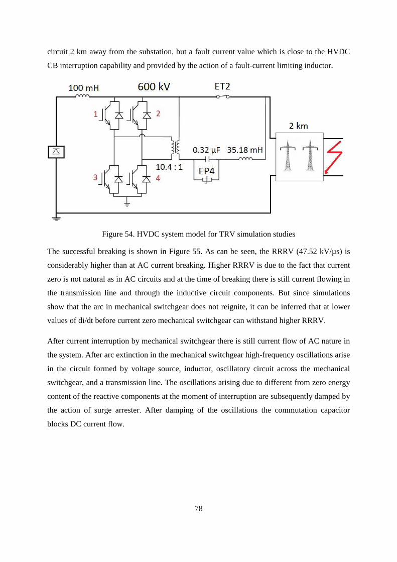
78
circuit 2 km away from the substation, but a fault current value which is close to the HVDC
CB interruption capability and provided by the action of a fault-current limiting inductor.
Figure 54. HVDC system model for TRV simulation studies
The successful breaking is shown in Figure 55. As can be seen, the RRRV (47.52 kV/µs) is
considerably higher than at AC current breaking. Higher RRRV is due to the fact that current
zero is not natural as in AC circuits and at the time of breaking there is still current flowing in
the transmission line and through the inductive circuit components. But since simulations
show that the arc in mechanical switchgear does not reignite, it can be inferred that at lower
values of di/dt before current zero mechanical switchgear can withstand higher RRRV.
After current interruption by mechanical switchgear there is still current flow of AC nature in
the system. After arc extinction in the mechanical switchgear high-frequency oscillations arise
in the circuit formed by voltage source, inductor, oscillatory circuit across the mechanical
switchgear, and a transmission line. The oscillations arising due to different from zero energy
content of the reactive components at the moment of interruption are subsequently damped by
the action of surge arrester. After damping of the oscillations the commutation capacitor
blocks DC current flow.

79
Figure 55. Breaking process: DC 25.5 kA, AC impulse 25.51 kA
A false analogy can be drawn between the DC switching by an oscillation CB and switching
of AC with delayed current zeroes. In principle there is a superposition of DC and AC current
components in both cases. However, in a DC circuit the recovery voltage rises not with the
network frequency but in much steeper manner. Therefore, if SF6 puffer-type switchgear is
used, the interruption must be performed within the first 25 ms after contact separation, when
the breaking capability is maximum.
Figure 56 illustrates that no high-frequency oscillations caused by the travelling waves on the
line side are observed in the breaking process under study. They are smoothed by L and C
components of the oscillatory circuit. Actually there is no chance for a travelling wave to
reflect from the CB terminal, because no open circuit at the CB line terminal is available.
Therefore, DC switching has no such an issue as short-circuit fault, which is peculiar to AC
networks.
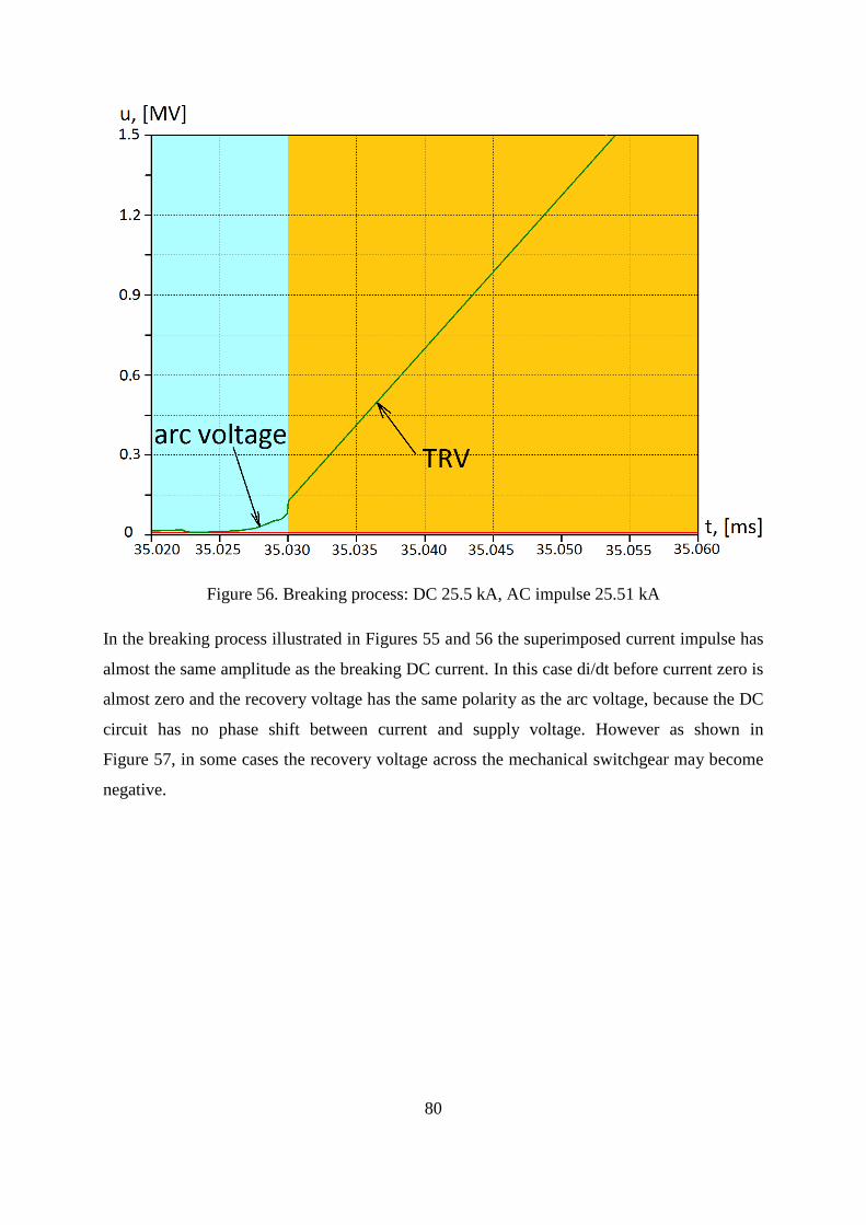
80
Figure 56. Breaking process: DC 25.5 kA, AC impulse 25.51 kA
In the breaking process illustrated in Figures 55 and 56 the superimposed current impulse has
almost the same amplitude as the breaking DC current. In this case di/dt before current zero is
almost zero and the recovery voltage has the same polarity as the arc voltage, because the DC
circuit has no phase shift between current and supply voltage. However as shown in
Figure 57, in some cases the recovery voltage across the mechanical switchgear may become
negative.
81
Figure 57. Breaking process: DC 25.5 kA, AC impulse 25.52 kA
The negative half-wave of the TRV in Figure 57 is caused by the fact that in this switching
case the AC-current oscillation amplitude is slightly higher than the breaking current. As the
mechanical switchgear managed to withstand a very steep TRV, commutation of the AC - DC
current difference from the oscillatory circuit into the current path formed by the source and
transmission line produces this negative half-wave. The higher the difference between the AC
and DC currents, the greater is di/dt before current zero and the steeper is du/dt consequently.
Starting from certain threshold value of di/dt before current zero the resulting du/dt cannot be
withstood by mechanical switchgear, which leads to a reignition of the arc. In a particular
network configuration shown in Figure 54, the arc reignites if di/dt before current zero is
higher than 2.7 A/µs.
Thus, the better matching of the breaking current and current impulse mitigates switching
conditions for oscillation-type HVDC CB. It holds true for both di/dt and du/dt aspects.
Therefore, for an oscillation HVDC CB a higher oscillation frequency is preferred to provide
a more accurate matching of DC and AC magnitudes.
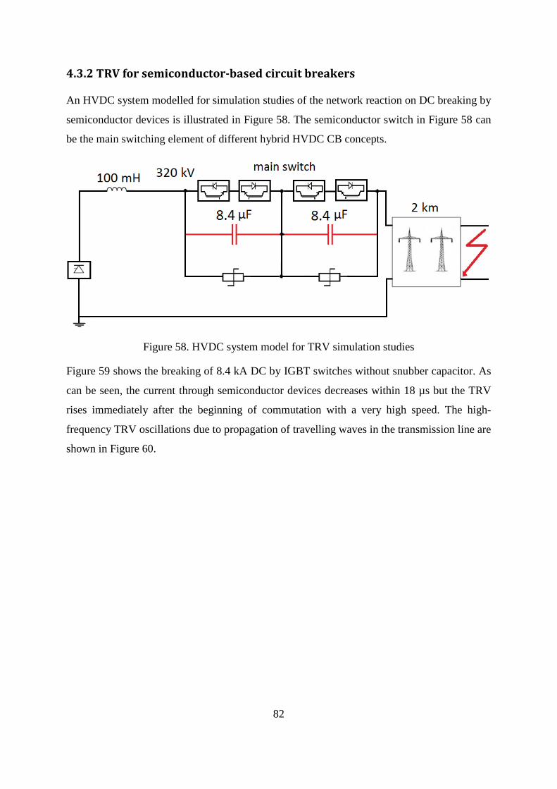
82
4.3.2 TRV for semiconductor-based circuit breakers
An HVDC system modelled for simulation studies of the network reaction on DC breaking by
semiconductor devices is illustrated in Figure 58. The semiconductor switch in Figure 58 can
be the main switching element of different hybrid HVDC CB concepts.
Figure 58. HVDC system model for TRV simulation studies
Figure 59 shows the breaking of 8.4 kA DC by IGBT switches without snubber capacitor. As
can be seen, the current through semiconductor devices decreases within 18 µs but the TRV
rises immediately after the beginning of commutation with a very high speed. The high-
frequency TRV oscillations due to propagation of travelling waves in the transmission line are
shown in Figure 60.
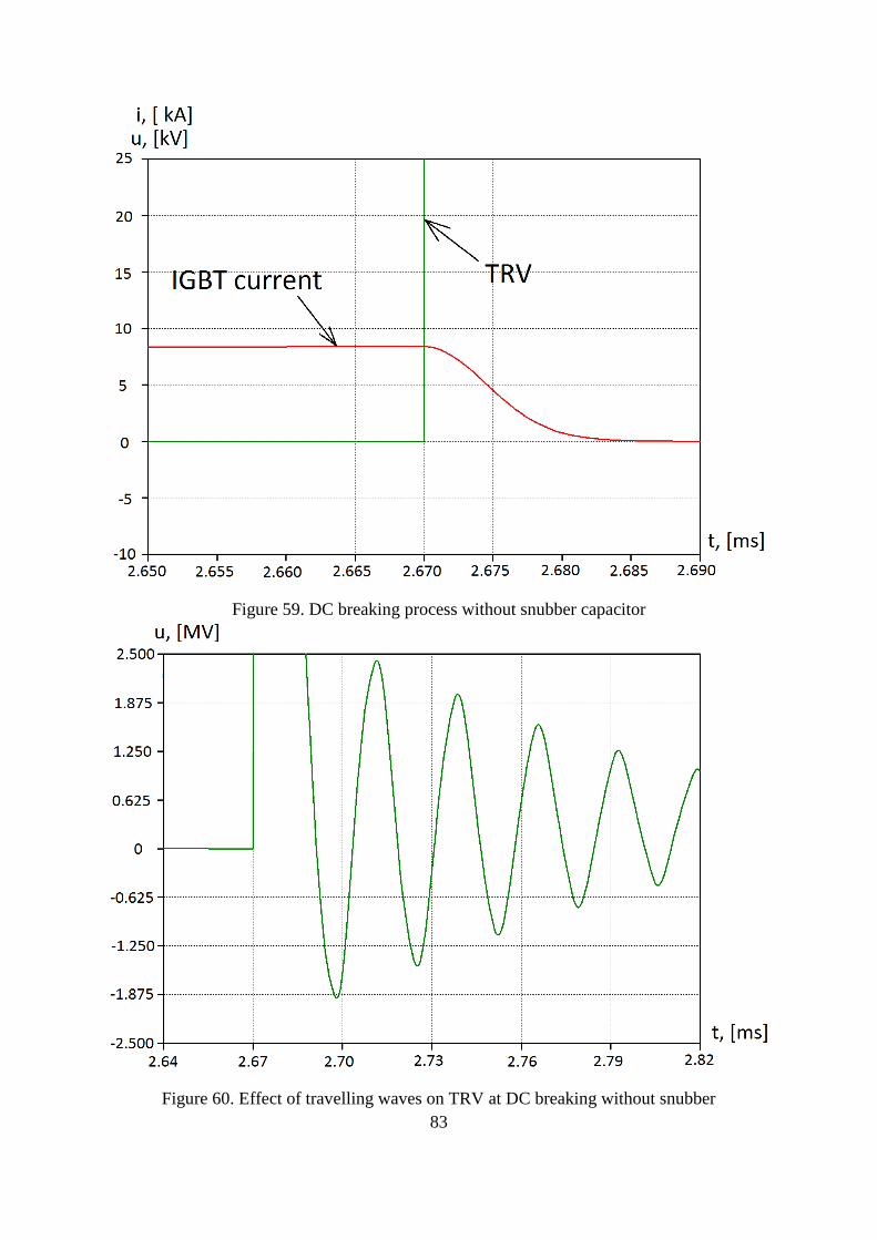
83
Figure 59. DC breaking process without snubber capacitor
Figure 60. Effect of travelling waves on TRV at DC breaking without snubber
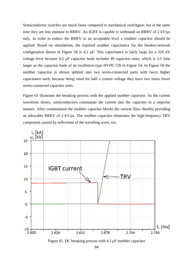
84
Semiconductor switches are much faster compared to mechanical switchgear, but at the same
time they are less immune to RRRV. An IGBT is capable to withstand an RRRV of 2 kV/µs
only. In order to reduce the RRRV to an acceptable level a snubber capacitor should be
applied. Based on simulations, the required snubber capacitance for the breaker-network
configuration shown in Figure 58 is 4.2 µF. This capacitance is fairly large for a 320 kV
voltage level because 4.2 µF capacitor bank includes 49 capacitor units, which is 3.5 time
larger as the capacitor bank of an oscillation-type HVDC CB in Figure 54. In Figure 58 the
snubber capacitor is shown splitted into two series-connected parts with twice higher
capacitance each, because being rated for half a system voltage they have two times fewer
series-connected capacitor units.
Figure 61 illustrates the breaking process with the applied snubber capacitor. As the current
waveform shows, semiconductors commutate the current into the capacitor in a stepwise
manner. After commutation the snubber capacitor blocks the current flow, thereby providing
an allowable RRRV of 2 kV/µs. The snubber capacitor eliminates the high-frequency TRV
component caused by reflections of the travelling wave, too.
Figure 61. DC breaking process with 4.2 µF snubber capacitor

85
Operation of a fast mechanical disconnector (FMD) in the ABB hybrid HVDC CB concept
resembles small inductive current switching. FMD switches practically no current, but after
switching the FMD has to withstand a very steep RRRV. However, since a RRRV of 2 kV/µs
must be secured for semiconductor devices by a snubber capacitor, it should not be a problem
for standard SF6 switchgear to withstand the recovery voltage after operation of the main
switch. Thus, there is no necessity to develop some complicated FMD devices as the one
illustrated in Figures 5 and 6. For application in hybrid HVDC CB an SF6 switchgear with
two moving contacts can be selected to provide faster contact separation. A time chart in
Figure 62 explains the particulars of using SF6 switchgear with two moving contacts in the
ABB HVDC CB concept.
Figure 62. Time chart of current interruption by hybrid ABB HVDC CB using SF6 switchgear with two moving contacts
As known, with two moving contacts the separation speed is 150% higher. Taking a moderate
RRRV into account, a partial opening of the SF6 switchgear contacts can be sufficient in
order to withstand recovery voltage. If necessary, the current limitation capability of IGBTs in
the main switch or current limitation by a series inductor can be used to provide the time
necessary for sufficient contact separation.
4.3.3 Recovery voltage grading and TRV peak shaving
The present section deals with such TRV issues as voltage grading across interrupter units of
mechanical switchgear and the suppression of TRV peak.
A trivial way of overvoltage limitation in high-voltage networks is the use of surge arresters.
Surge arresters could be used in HVDC networks for mitigation of voltage switching
transients, too. Mainly, there are two components of an HVDC CB to be protected from the
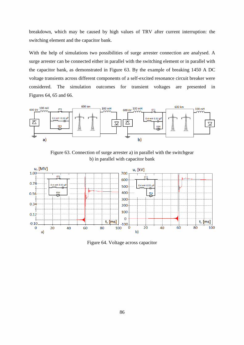
86
breakdown, which may be caused by high values of TRV after current interruption: the
switching element and the capacitor bank.
With the help of simulations two possibilities of surge arrester connection are analysed. A
surge arrester can be connected either in parallel with the switching element or in parallel with
the capacitor bank, as demonstrated in Figure 63. By the example of breaking 1450 A DC
voltage transients across different components of a self-excited resonance circuit breaker were
considered. The simulation outcomes for transient voltages are presented in
Figures 64, 65 and 66.
Figure 63. Connection of surge arrester a) in parallel with the switchgear b) in parallel with capacitor bank
Figure 64. Voltage across capacitor
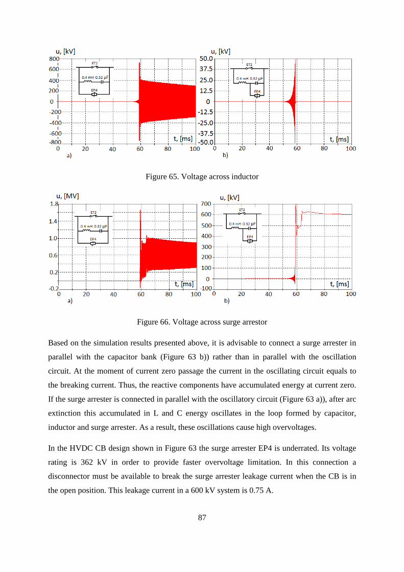
87
Figure 65. Voltage across inductor
Figure 66. Voltage across surge arrestor
Based on the simulation results presented above, it is advisable to connect a surge arrester in
parallel with the capacitor bank (Figure 63 b)) rather than in parallel with the oscillation
circuit. At the moment of current zero passage the current in the oscillating circuit equals to
the breaking current. Thus, the reactive components have accumulated energy at current zero.
If the surge arrester is connected in parallel with the oscillatory circuit (Figure 63 a)), after arc
extinction this accumulated in L and C energy oscillates in the loop formed by capacitor,
inductor and surge arrester. As a result, these oscillations cause high overvoltages.
In the HVDC CB design shown in Figure 63 the surge arrester EP4 is underrated. Its voltage
rating is 362 kV in order to provide faster overvoltage limitation. In this connection a
disconnector must be available to break the surge arrester leakage current when the CB is in
the open position. This leakage current in a 600 kV system is 0.75 A.
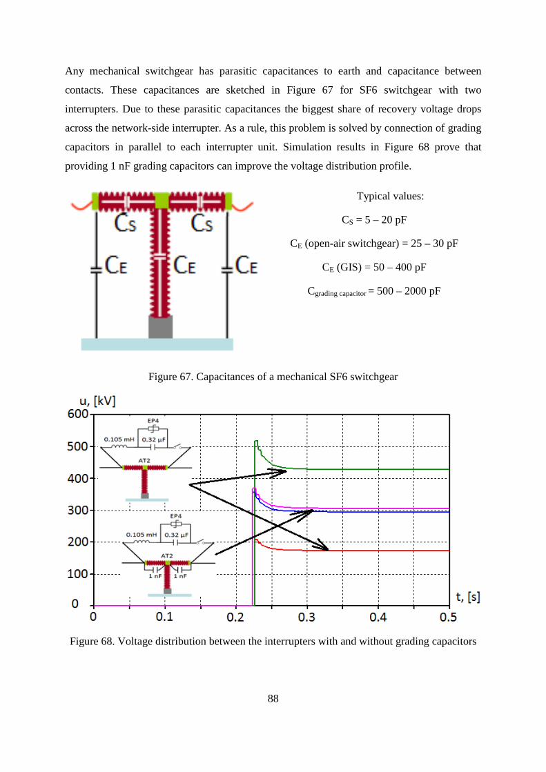
88
Any mechanical switchgear has parasitic capacitances to earth and capacitance between
contacts. These capacitances are sketched in Figure 67 for SF6 switchgear with two
interrupters. Due to these parasitic capacitances the biggest share of recovery voltage drops
across the network-side interrupter. As a rule, this problem is solved by connection of grading
capacitors in parallel to each interrupter unit. Simulation results in Figure 68 prove that
providing 1 nF grading capacitors can improve the voltage distribution profile.
Typical values:
CS = 5 – 20 pF
CE (open-air switchgear) = 25 – 30 pF
CE (GIS) = 50 – 400 pF
Cgrading capacitor = 500 – 2000 pF
Figure 67. Capacitances of a mechanical SF6 switchgear
Figure 68. Voltage distribution between the interrupters with and without grading capacitors
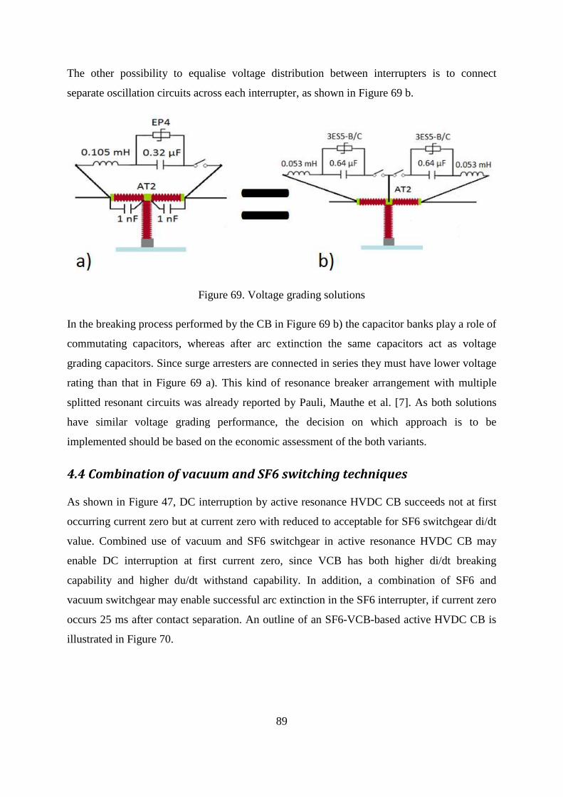
89
The other possibility to equalise voltage distribution between interrupters is to connect
separate oscillation circuits across each interrupter, as shown in Figure 69 b.
Figure 69. Voltage grading solutions
In the breaking process performed by the CB in Figure 69 b) the capacitor banks play a role of
commutating capacitors, whereas after arc extinction the same capacitors act as voltage
grading capacitors. Since surge arresters are connected in series they must have lower voltage
rating than that in Figure 69 a). This kind of resonance breaker arrangement with multiple
splitted resonant circuits was already reported by Pauli, Mauthe et al. [7]. As both solutions
have similar voltage grading performance, the decision on which approach is to be
implemented should be based on the economic assessment of the both variants.
4.4 Combination of vacuum and SF6 switching techniques
As shown in Figure 47, DC interruption by active resonance HVDC CB succeeds not at first
occurring current zero but at current zero with reduced to acceptable for SF6 switchgear di/dt
value. Combined use of vacuum and SF6 switchgear in active resonance HVDC CB may
enable DC interruption at first current zero, since VCB has both higher di/dt breaking
capability and higher du/dt withstand capability. In addition, a combination of SF6 and
vacuum switchgear may enable successful arc extinction in the SF6 interrupter, if current zero
occurs 25 ms after contact separation. An outline of an SF6-VCB-based active HVDC CB is
illustrated in Figure 70.
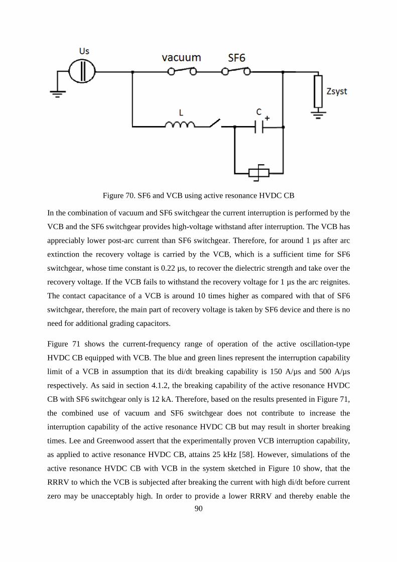
90
Figure 70. SF6 and VCB using active resonance HVDC CB
In the combination of vacuum and SF6 switchgear the current interruption is performed by the
VCB and the SF6 switchgear provides high-voltage withstand after interruption. The VCB has
appreciably lower post-arc current than SF6 switchgear. Therefore, for around 1 µs after arc
extinction the recovery voltage is carried by the VCB, which is a sufficient time for SF6
switchgear, whose time constant is 0.22 µs, to recover the dielectric strength and take over the
recovery voltage. If the VCB fails to withstand the recovery voltage for 1 µs the arc reignites.
The contact capacitance of a VCB is around 10 times higher as compared with that of SF6
switchgear, therefore, the main part of recovery voltage is taken by SF6 device and there is no
need for additional grading capacitors.
Figure 71 shows the current-frequency range of operation of the active oscillation-type
HVDC CB equipped with VCB. The blue and green lines represent the interruption capability
limit of a VCB in assumption that its di/dt breaking capability is 150 A/µs and 500 A/µs
respectively. As said in section 4.1.2, the breaking capability of the active resonance HVDC
CB with SF6 switchgear only is 12 kA. Therefore, based on the results presented in Figure 71,
the combined use of vacuum and SF6 switchgear does not contribute to increase the
interruption capability of the active resonance HVDC CB but may result in shorter breaking
times. Lee and Greenwood assert that the experimentally proven VCB interruption capability,
as applied to active resonance HVDC CB, attains 25 kHz [58]. However, simulations of the
active resonance HVDC CB with VCB in the system sketched in Figure 10 show, that the
RRRV to which the VCB is subjected after breaking the current with high di/dt before current
zero may be unacceptably high. In order to provide a lower RRRV and thereby enable the

91
VCB to withstand it, the di/dt before current zero must be lower. This fact means that there is
no point in the combined use of vacuum and SF6 switchgear in oscillation-type HVDC CB.
Figure 71. Performance curves of vacuum interrupter and LC-circuit
The other possibility to take advantage of the combination of vacuum and SF6 switchgear is
shown in Figure 72. In this hybrid HVDC CB configuration the VCB has to develop the arc
voltage of 100-150 V only, which is possible for a 72 kV vacuum tube. A current limiting
inductor serves to secure the short-circuit current value after fault initiation within the limits
of IGBT breaking capability. The main switch operates after the VCB sufficiently separated
its contacts in order to develop the required commutation voltage. After operation of the main
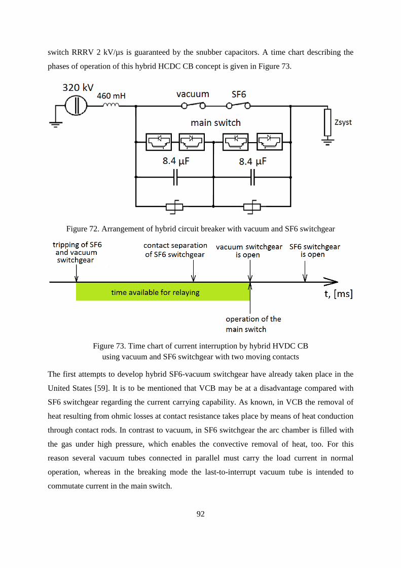
92
switch RRRV 2 kV/µs is guaranteed by the snubber capacitors. A time chart describing the
phases of operation of this hybrid HCDC CB concept is given in Figure 73.
Figure 72. Arrangement of hybrid circuit breaker with vacuum and SF6 switchgear
Figure 73. Time chart of current interruption by hybrid HVDC CB using vacuum and SF6 switchgear with two moving contacts
The first attempts to develop hybrid SF6-vacuum switchgear have already taken place in the
United States [59]. It is to be mentioned that VCB may be at a disadvantage compared with
SF6 switchgear regarding the current carrying capability. As known, in VCB the removal of
heat resulting from ohmic losses at contact resistance takes place by means of heat conduction
through contact rods. In contrast to vacuum, in SF6 switchgear the arc chamber is filled with
the gas under high pressure, which enables the convective removal of heat, too. For this
reason several vacuum tubes connected in parallel must carry the load current in normal
operation, whereas in the breaking mode the last-to-interrupt vacuum tube is intended to
commutate current in the main switch.
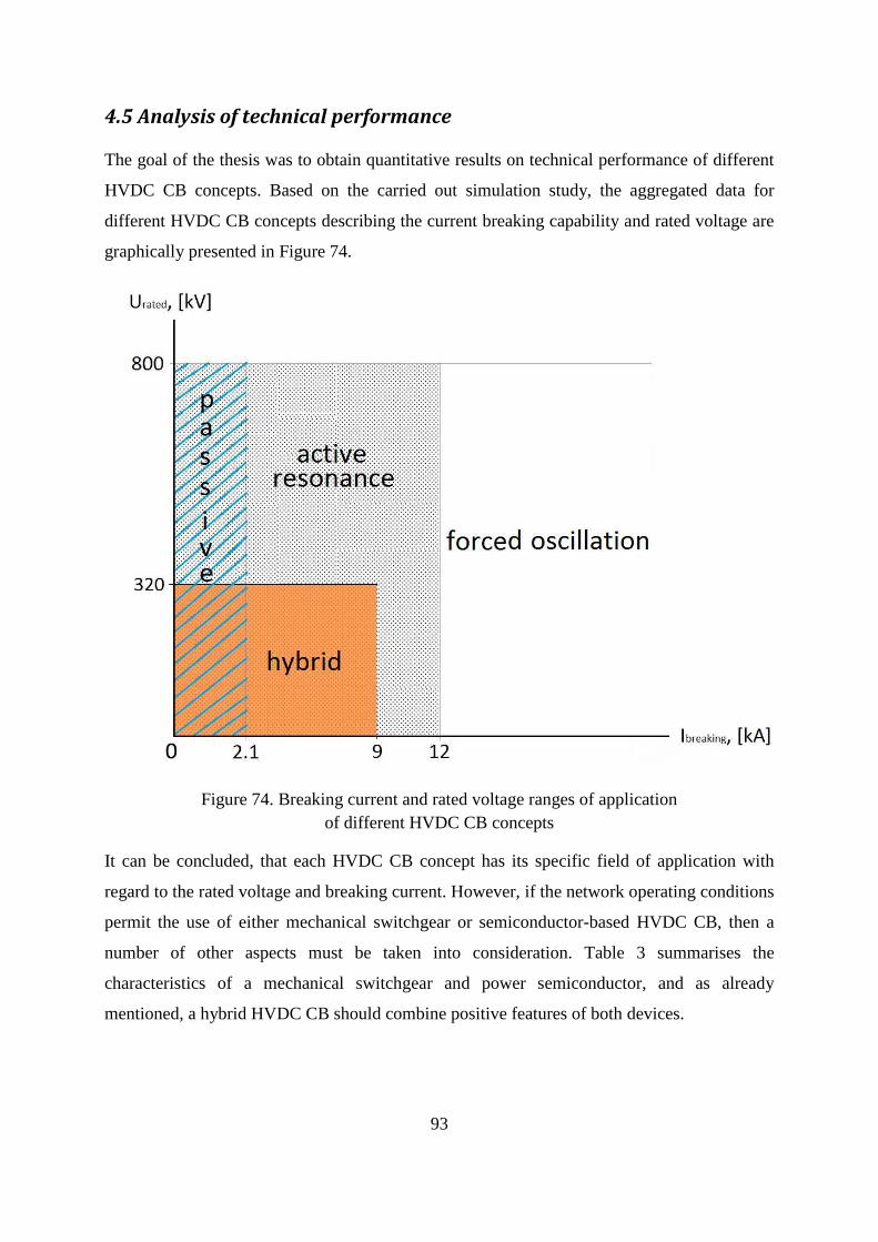
93
4.5 Analysis of technical performance
The goal of the thesis was to obtain quantitative results on technical performance of different
HVDC CB concepts. Based on the carried out simulation study, the aggregated data for
different HVDC CB concepts describing the current breaking capability and rated voltage are
graphically presented in Figure 74.
Figure 74. Breaking current and rated voltage ranges of application of different HVDC CB concepts
It can be concluded, that each HVDC CB concept has its specific field of application with
regard to the rated voltage and breaking current. However, if the network operating conditions
permit the use of either mechanical switchgear or semiconductor-based HVDC CB, then a
number of other aspects must be taken into consideration. Table 3 summarises the
characteristics of a mechanical switchgear and power semiconductor, and as already
mentioned, a hybrid HVDC CB should combine positive features of both devices.

94
Table 3. Comparison of HVDC mechanical switchgear and semiconductor devices
Mechanical switchgear Power electronics switch
Operating speed slow fast
Resistance and steady-state losses
low increased
Need for cooling no yes
Overload capability high restricted
Current flow reversal easily impossible
Overvoltage sensitivity low high
Need for protection circuit no yes
Galvanic isolation yes no
Leakage current no yes
Scalability scalable up to 1100 kV (4 interrupters)
scalable up to 320 kV
Installation type indoors and outdoors indoors
Dimensions and volume compact and small relatively big due to cooling requirement
Maintenance required not required
Environmental considerations SF6 favourable
Life expectancy limited theoretically unlimited

95
A line should be drawn between two potential markets for HVDC circuit breakers. These
markets will have different network structure and can be defined as the European and Asian
markets. The tabulated design particulars of the European and Asian HVDC networks are
presented below.
Table 4. Characteristics of the prospective HVDC transmission systems with regard to regional specifics
Europe Rest of the world
Voltage Up to 320 kV Up to 1100
Transmission distances
Lines up to 600 km Lines up to 2000 km
Type of transmission lines
Mix of overhead and cable sections Predominance of overhead transmission lines
Converter design
VSC-convertors prevail LCC-convertors prevail
Network density
Highly meshed network structure Moderately meshed network structure
Place of deployment
Offshore and onshore lines and substations
Onshore lines and substations
From the point of view of economics, application of an HVDC CB for the purpose of network
protection is reasonable as long as it is cheaper than the construction of an HVDC converter
substation [60]. Taking into account HVDC substation investment costs, which constitute 40
MEUR for 500 MW LCC-substation [60], it turns out that there is a wide field for manoeuvre
in designing an HVDC CB, which can be 250 times more expensive per 1 kV of rated voltage
than its SF6 AC-colleague. However, different network specifics may require different design
approaches to HVDC circuit breakers. The diagram in Figure 75 describes the rated
parameters of the prospective HVDC grids.

96
Figure 75. Ranges of the DC grid ratings
On the basis of matching of the voltage ranges in Figure 74 and Figure 75, it can be concluded
that the European network can be protected by semiconductor or mechanical switchgear-
based HVDC CB. A set of simulations showed that the oscillation-type HVDC CBs can be
successfully used for cable switching, since the current impulse produced by the oscillatory
circuit does not propagate into the cable due to its relatively low surge impedance. In its turn
HVDC CB for Asian grids should be based on the mechanical switching elements.

97
5 Protection solutions for HVDC network
There are four main technical characteristics of a circuit breaker, namely:
- Rated voltage
- Rated normal current
- Breaking current
- Breaking time
The first three characteristics in the list above were analysed in the preceding chapter,
whereupon the breaking capabilities and current-voltage ranges of application of different
HVDC CB concepts were presented. This chapter focuses on the breaking time.
The benefits of short interruption time are explained in Figure 3 with regard to a circuit
breaker as a device. The present chapter aims at answering the question how fast an HVDC
CB should be as required by the network. The statements made in this chapter by no means
pretend to be dogmatic, but rather serve as a basis for further discussion, because there are
still no standards on the HVDC grid, and each HVDC project is to some extent unique.
5.1 Interaction of circuit breaker and DC voltage control system
The problem of the required breaking time as applied to the HVDC network can be
categorised into two issues: system stability and converter protection.
• At short circuit the voltage profile of the network changes substantially. The voltage
reduces and thereby hinders normal power exchange between the rectifier and inverter
substations. As a result the power system may lose stability of operation. However, the
question how long the power system can keep stability under fault conditions is still
open. In order to impose substantiated requirements to an HVDC CB with regard to
breaking time, the question of the power system fault ride-through capability must be
clarified, but this aspect is beyond the scope of this thesis.
• A high short-circuit current may overheat and destroy power semiconductor
components of a convertor. Therefore, a short circuit must be cleared within few
milliseconds [61]. Mainly, in VSC HVDC the free-wheeling diodes of the IGBT-
modules (Figure 76) are jeopardised. Thyristors in LCC converters are more immune
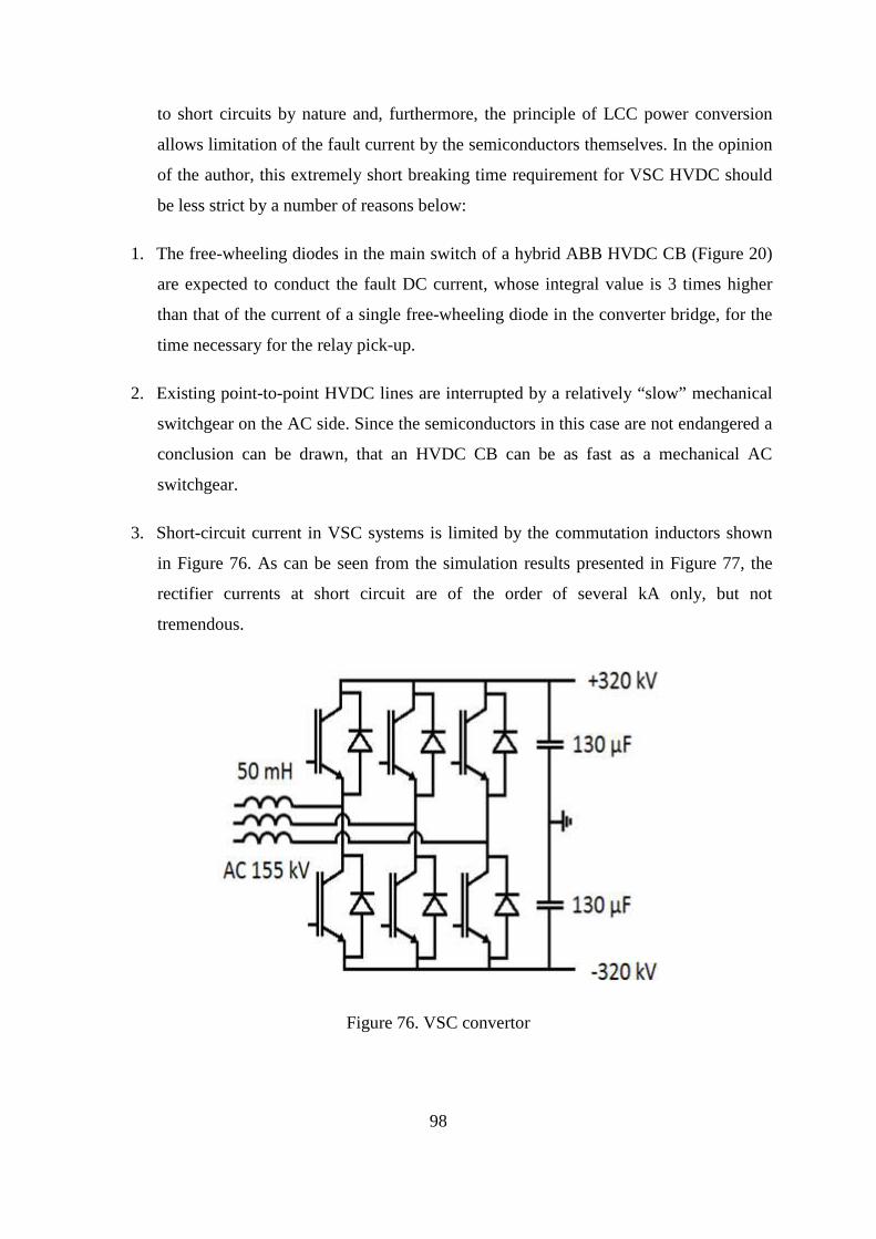
98
to short circuits by nature and, furthermore, the principle of LCC power conversion
allows limitation of the fault current by the semiconductors themselves. In the opinion
of the author, this extremely short breaking time requirement for VSC HVDC should
be less strict by a number of reasons below:
1. The free-wheeling diodes in the main switch of a hybrid ABB HVDC CB (Figure 20)
are expected to conduct the fault DC current, whose integral value is 3 times higher
than that of the current of a single free-wheeling diode in the converter bridge, for the
time necessary for the relay pick-up.
2. Existing point-to-point HVDC lines are interrupted by a relatively “slow” mechanical
switchgear on the AC side. Since the semiconductors in this case are not endangered a
conclusion can be drawn, that an HVDC CB can be as fast as a mechanical AC
switchgear.
3. Short-circuit current in VSC systems is limited by the commutation inductors shown
in Figure 76. As can be seen from the simulation results presented in Figure 77, the
rectifier currents at short circuit are of the order of several kA only, but not
tremendous.
Figure 76. VSC convertor
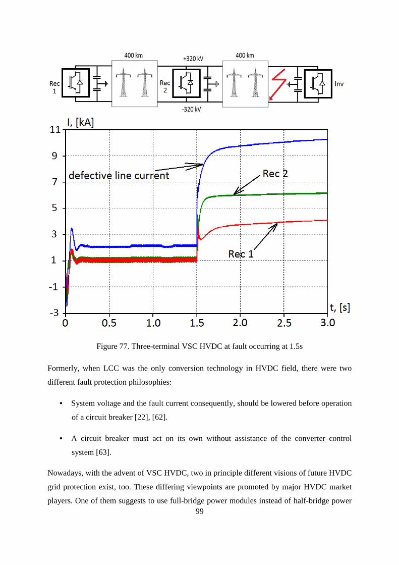
99
Figure 77. Three-terminal VSC HVDC at fault occurring at 1.5s
Formerly, when LCC was the only conversion technology in HVDC field, there were two
different fault protection philosophies:
• System voltage and the fault current consequently, should be lowered before operation
of a circuit breaker [22], [62].
• A circuit breaker must act on its own without assistance of the converter control
system [63].
Nowadays, with the advent of VSC HVDC, two in principle different visions of future HVDC
grid protection exist, too. These differing viewpoints are promoted by major HVDC market
players. One of them suggests to use full-bridge power modules instead of half-bridge power
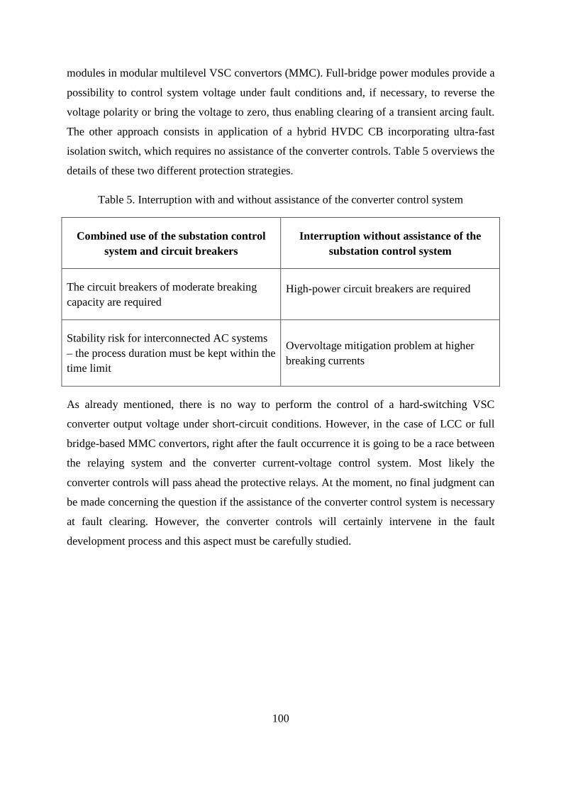
100
modules in modular multilevel VSC convertors (MMC). Full-bridge power modules provide a
possibility to control system voltage under fault conditions and, if necessary, to reverse the
voltage polarity or bring the voltage to zero, thus enabling clearing of a transient arcing fault.
The other approach consists in application of a hybrid HVDC CB incorporating ultra-fast
isolation switch, which requires no assistance of the converter controls. Table 5 overviews the
details of these two different protection strategies.
Table 5. Interruption with and without assistance of the converter control system
Combined use of the substation control system and circuit breakers
Interruption without assistance of the substation control system
The circuit breakers of moderate breaking capacity are required
High-power circuit breakers are required
Stability risk for interconnected AC systems – the process duration must be kept within the time limit
Overvoltage mitigation problem at higher breaking currents
As already mentioned, there is no way to perform the control of a hard-switching VSC
converter output voltage under short-circuit conditions. However, in the case of LCC or full
bridge-based MMC convertors, right after the fault occurrence it is going to be a race between
the relaying system and the converter current-voltage control system. Most likely the
converter controls will pass ahead the protective relays. At the moment, no final judgment can
be made concerning the question if the assistance of the converter control system is necessary
at fault clearing. However, the converter controls will certainly intervene in the fault
development process and this aspect must be carefully studied.
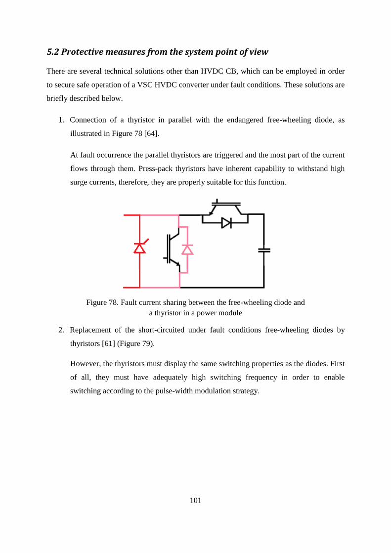
101
5.2 Protective measures from the system point of view
There are several technical solutions other than HVDC CB, which can be employed in order
to secure safe operation of a VSC HVDC converter under fault conditions. These solutions are
briefly described below.
1. Connection of a thyristor in parallel with the endangered free-wheeling diode, as
illustrated in Figure 78 [64].
At fault occurrence the parallel thyristors are triggered and the most part of the current
flows through them. Press-pack thyristors have inherent capability to withstand high
surge currents, therefore, they are properly suitable for this function.
Figure 78. Fault current sharing between the free-wheeling diode and a thyristor in a power module
2. Replacement of the short-circuited under fault conditions free-wheeling diodes by
thyristors [61] (Figure 79).
However, the thyristors must display the same switching properties as the diodes. First
of all, they must have adequately high switching frequency in order to enable
switching according to the pulse-width modulation strategy.

102
Figure 79. VSC convertor with free-wheeling thyristors
3. The use of full-bridge power mudules in MMC VSC convertors.
Four-quadrant operating power modules enable limitation of the fault current by
capacitors.
Figure 80. a) two-quadrant operating power module b) four-quadrant operating power module
4. The use of DC-DC convertors and DC-DC choppers as circuit breakers [65].
This approach enables fast current breaking and in the case of DC-DC converter
galvanic isolation, too. The use of DC-DC choppers or convertors provides also a
possibility for regulation of the current flow in HVDC network, which still remains an

103
unsolved problem [60]. However, an operation of DC-DC choppers and convertors is
associated with additional power conversion losses.
Figure 81. A bidirectional DC-to-DC convertor
Figure 82. The four-switch DC-DC chopper
5. Application of fault current limiters.
Fault current limiters reduce the rate of rise of fault current, thereby protecting the
converter semiconductor components and at the same time reducing the current to be
interrupted by a circuit breaker. The application of fault current limiters is discussed in
the following chapter in more details.

104
5.3 Interaction between fault current limiter and a convertor
In the variety of available fault current limitation techniques the use of an inductor is the most
straightforward solution. The only adjustable parameter of such a fault current limiter (FCL)
is its inductance, which has to be constant in the whole current range of application of an
FCL. Therefore, air-core reactors are preferable to metal-core ones that may saturate. The
flow chart in Figure 83 facilitates the decision making regarding the need to apply a fault
current limiter.
Figure 83. Identification of the necessity for a fault current limiter
At the substation a fault current limiting reactor can be located either on the high-voltage side
or at ground potential. It is not, however, possible to install only one reactor at zero potential,
because some small inductance must be available on the high-voltage pole in order to protect
semiconductor switches from the lightning strokes. The size of this blocking reactor must be
at least 5-10 mH [2]. As a rule savings on insulation do not cover installation of two
inductors, therefore, in most cases only one reactor of the required size is installed on the
high-voltage side [66].
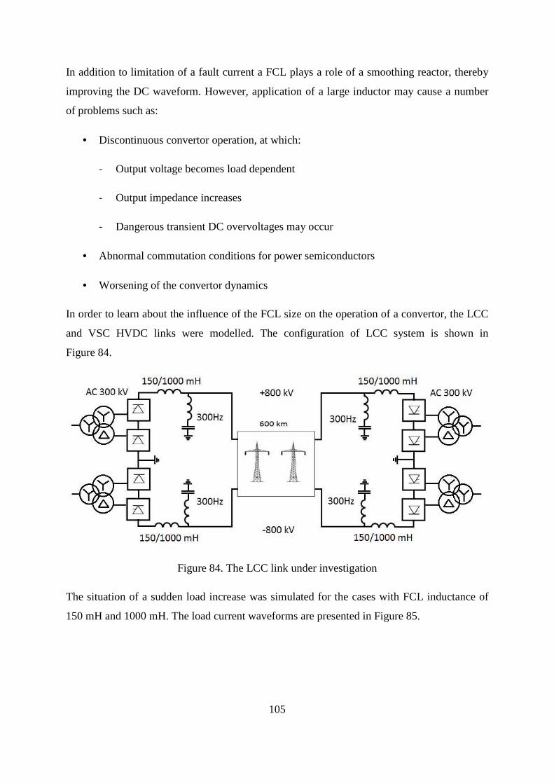
105
In addition to limitation of a fault current a FCL plays a role of a smoothing reactor, thereby
improving the DC waveform. However, application of a large inductor may cause a number
of problems such as:
• Discontinuous convertor operation, at which:
- Output voltage becomes load dependent
- Output impedance increases
- Dangerous transient DC overvoltages may occur
• Abnormal commutation conditions for power semiconductors
• Worsening of the convertor dynamics
In order to learn about the influence of the FCL size on the operation of a convertor, the LCC
and VSC HVDC links were modelled. The configuration of LCC system is shown in
Figure 84.
Figure 84. The LCC link under investigation
The situation of a sudden load increase was simulated for the cases with FCL inductance of
150 mH and 1000 mH. The load current waveforms are presented in Figure 85.
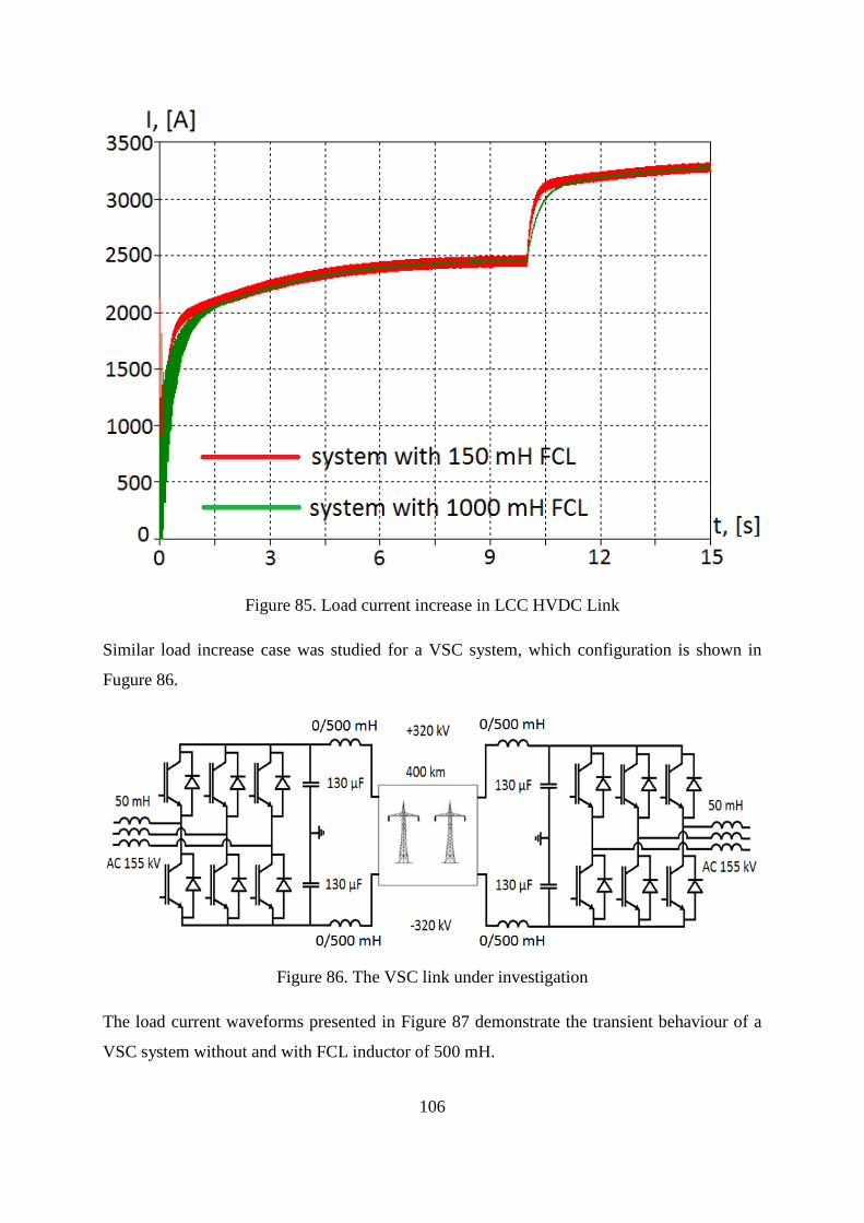
106
Figure 85. Load current increase in LCC HVDC Link
Similar load increase case was studied for a VSC system, which configuration is shown in
Fugure 86.
Figure 86. The VSC link under investigation
The load current waveforms presented in Figure 87 demonstrate the transient behaviour of a
VSC system without and with FCL inductor of 500 mH.
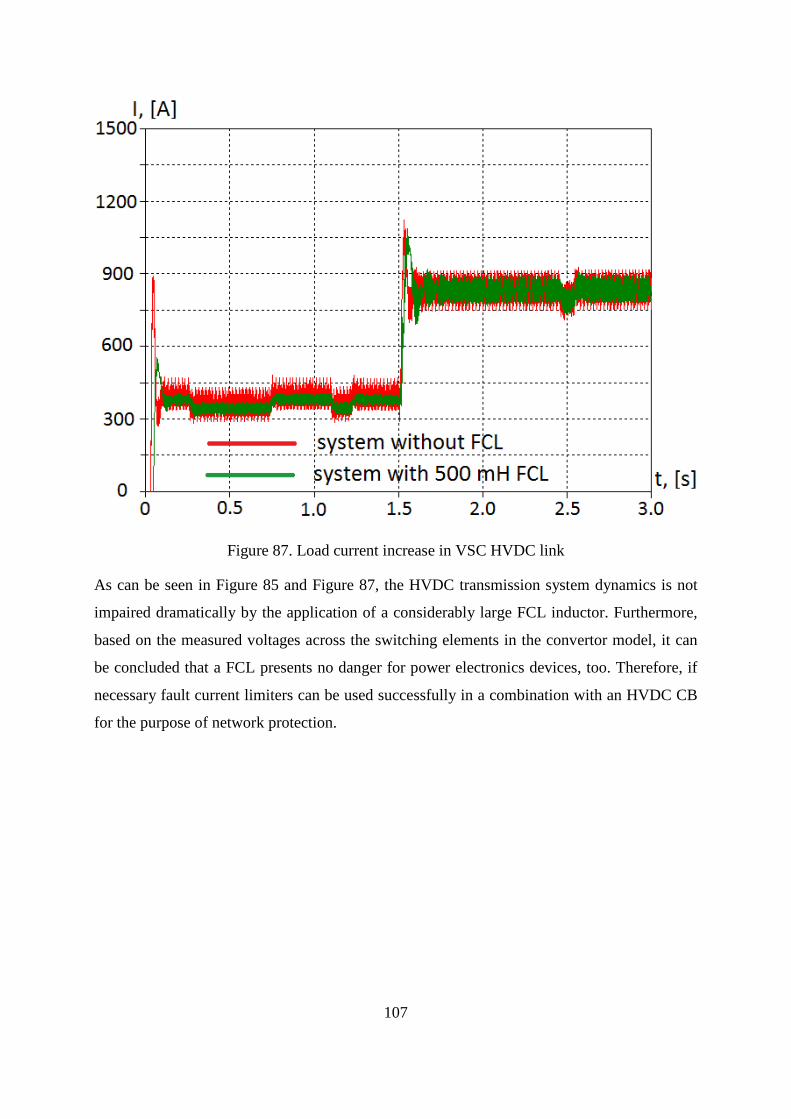
107
Figure 87. Load current increase in VSC HVDC link
As can be seen in Figure 85 and Figure 87, the HVDC transmission system dynamics is not
impaired dramatically by the application of a considerably large FCL inductor. Furthermore,
based on the measured voltages across the switching elements in the convertor model, it can
be concluded that a FCL presents no danger for power electronics devices, too. Therefore, if
necessary fault current limiters can be used successfully in a combination with an HVDC CB
for the purpose of network protection.
108
6 Conclusions and recommendations
The aim of this thesis was to analyse the technical performance of different HVDC CB
concepts with the help of numerical simulations. The term “technical performance”
encompasses the current breaking and recovery voltage withstand capabilities as well as
operation time. Economics-related aspects such as on-state power losses, circuit breaker
dimensions etc. are also touched upon. Conclusions and recommendations resulting from the
carried out research work are summarised in the two following sub-chapters.
6.1 Summary and contributions
The main results gained in the course of this research work are presented below in the thesis
form:
• The definition of breaking capability of an HVDC CB is different from that of an AC
mechanical switchgear. The breaking capability of the AC mechanical switchgear is
determined by the device capability to interrupt current with certain di/dt value before
current zero and to withstand the appearing du/dt of the recovery voltage. In the
context of HVDC CB the breaking capability is defined as the ability of the device
either to produce a sufficient current impulse intended to produce current zero or the
ability of a semiconductor-based switching element to switch off the current. The di/dt
and the du/dt are separate aspects for an HVDC CB.
• The breaking capability of a mechanical HVDC CB may attain a few tens of kA and is
limited by the capability of the oscillatory circuit to produce current zero. The
breaking time must be shorter than 25 ms due to the decrease of the breaking
capability of the SF6 switchgear at longer arcing times. The breaking capability of a
semiconductor-based HVDC CB is 9 kA and is determined by the switching capability
of semiconductor devices.
• Higher-frequency oscillations of the commutation current are acceptable, because the
breaking current approaches zero with a very low di/dt.
• Mechanical switchgear can withstand much higher RRRV as compared with the AC
switching, because in HVDC CB the breaking current approaches zero with a very low
di/dt.
109
• After current breaking equal voltage distribution between the interrupters of the SF6
switchgear can be achieved by the use of voltage grading capacitors. Alternatively, a
separate oscillatory circuit can be provided for each interrupter.
• For more a effective limitation of the switching overvoltages it is preferred to connect
surge arrester in parallel with the capacitor bank.
• Conventional SF6 switchgear may be used in the hybrid HVDC CB concept of ABB
instead of a fast mechanical disconnector.
• There is no use of vacuum and SF6 switchgear combination in mechanical HVDC CB,
although it can be a promising solution for hybrid concept illustrated in Figure 72.
• An HVDC CB should not be faster than a conventional SF6 switchgear from the point
of view of converter safety. If necessary, converter protection techniques can be used
in order to guarantee safe operation of power semiconductors.
• A fault current limiter can be used for converter protection and for facilitation of the
fault clearing by the reduction of the short-circuit current to be interrupted by a circuit
breaker. Application of a FCL presents no danger for the converter components and
has no detrimental effects on both LCC and VSC converter operation.

110
6.2 Future research
The study performed within the scope of the present thesis covers a spectrum of questions
related to both HVDC CB itself and to the HVDC transmission grid. There are, however,
some other aspects deserving consideration, which must be studied in order to enable a
systematic approach to the design of an HVDC circuit breaker. For the future research it is
recommended to focus on the points presented in the list below:
• The immunity of the free-wheeling diodes in the IGBT-modules to the fault current
must be studied. The expected research outcome is then justified by the converter
safety breaking time requirement.
• HVDC system under fault conditions should be investigated in order to learn how the
DC voltage collapse influences the stability of the entire power grid. The aim of the
study is to specify the breaking time requirement dictated by the condition of stable
network operation.
• The manner of reaction of the HVDC network controls and the HVDC converter
controls on the DC short circuit must be studied, too. This study must give insight into
the fault current development process and, thus, define the requirements on an HVDC
CB performance.
• The subject to study further is the operating algorithms and the time of response of the
relaying system. The relaying time will serve for estimation of the projected fault
current value.
• The possibility of using a standard vacuum and SF6 switchgear in hybrid HVDC CB
topologies is of interest, too.
111
References
[1] A. Greenwood, K. W. Kanngiesser et al., "Circuit breakers for meshed multiterminal HVDC systems", ELECTRA, no. 163, pp. 99-122, 1995.
[2] J. Arrillaga, High voltage direct current transmission, London: Peregrinus, 1983.
[3] M. G. Bennett, N. S. Dhaliwal and A. Leirbukt, „A survey of the reliability of HVDC systems throughout the world during 200-2010“, CIGRE, Paris, 2012.
[4] R. Streich, „Einrichtung zum Abschalten von Gleichstrom-Hochspannungsleitungen“. Germany Patent 742715, 1940.
[5] P. Brückner, "Abschalten einer in Betrieb befindlichen Gleichstromleistung". Germany Patent B 207 592, 20 November 1944.
[6] G. A. Kukekov, P. G. Sorokin and N. A. Sipulina, "Switchgear for HVDC lines", Elektrichestwo, no. 3, pp. 24-27, 1959.
[7] B. Pauli, G. Mauthe et al., "Development of a high-current HVDC circuit breaker with fast fault clearing capability", IEEE Transactions on Power Delivery, vol. 3, no. 4, 1988.
[8] T. Senda, T. Tamagawa et al., "Development of HVDC circuit breaker based on hybrid interruption schemes", IEEE Transactions on Power Apparatus and Systems, Vols. PAS-103, no. 3, 1984.
[9] S. Tokuyama, K. Hirasawa et al., „Simulations on interruption of circuit breaker in HVDC system with two parallel transmission lines“, IEEE Transactions on Power Delivery, vol. PER-7, Nr. 7, 1987.
[10] J. Jadidian, "A Compact Design for High Voltage Direct Current Circuit Breaker", IEEE Transactions on Plasma Science, vol. 37, no. 6, 2009.
[11] J. Jadidian, K. Niayesh et al., "Numerical Simulation of an Explosively Driven HVDC Circuit Breaker", The Japan Society of Plasma Science and Nuclear Fusion Research, vol. 8, 2009.
[12] Z. Minghan and M. Yun, „Parameter estimation for HVDC circuit breaker“, in IEEE, 2011.
[13] A. Roshal, S. Avanesov et al., "Design and analysis of Switching Network Units for the ITER coil power supply System", Fusion Engineering and Design, vol. 86, no. 6-8, p. 1450–1453, 2011.

112
[14] B. Bareyt, "A 170-kA DC circuit breaker for the quench protection of the central solenoid coil of the ITER tokamak", Fusion Engineering and Design, vol. 54, no. 1, pp. 49-61, 2001.
[15] Å. Ekström, H. Härtel et al., "Design and testing of an HVDC circuit breaker", CIGRE, Paris, 1976.
[16] L. Liljestrand, "Switch having two sets of contact elements and two drives". Patent EP 2 511 928 A1, 17 October 2012.
[17] W. Pucher, P. Joss et al., „HVDC switching devices and arrangements“, ELECTRA, Nr. 18, pp. 9-65, 1971.
[18] R. W. Faulkner and R. Karnes, "Electromechanical ballistic DC breaker for use on ships", in IEEE Electric Ship Technical Symposium, Alexandria, VA USA, 2011.
[19] D. Imamovic, Interviewee, Gas-insulated switchgear for HVDC. [Interview]. 10 April 2014.
[20] J. Häfner and B. Jacobson, "Proactive hybrid HVDC breakers – A key innovation for reliable HVDC grids", in CIGRE Bologna Symposium, Bologna, 2011.
[21] Working Group 03 of Study Comittee No.13, „Application of HVDC circuit breakers“, ELECTRA, Nr. 31, pp. 53-64, 1973.
[22] K. W. Kanngiesser and B. Koetzold, „HVDC circuit breaker in intermeshed multi-terminal HVDC systems“, CIGRE session, Paris, 28 August – 6 September 1972.
[23] W. Pucher, "Fundamentals of HVDC interruption", ELECTRA, no. 5, pp. 24-39, 1968.
[24] N. D. Biryuk, Y. B. Nechaev and V. N. Finko, "Physical interpretation of parametric resonance, energy approach", Vestnik WGU, no. 1, pp. 20-25, 2005.
[25] A. M. Atmadji, "Direct current hybrid breakers: a design and its realization", Dissertation, Technische Universiteit Eindhoven, Eindhoven, 2000.
[26] M. Callavik, A. Blomberg et al., "Breakthrough! ABB’s hybrid HVDC breaker, an innovation breakthrough enabling reliable HVDC grids", ABB Review, no. 2, pp. 7-13, 2013.
[27] C. Meyer, S. Schröder and R. W. De Doncker, "Solid-state circuit breaker and current limiters for medium-voltage systems having distributed power systems", IEEE Transactions on Power Electronics, vol. 19, no. 5, 2004.
113
[28] E. I. Carroll, „Power electronics for very high power applications“, in s Power Electronics and Variable Speed Drives, 1998.
[29] M. H. Rashid, Power electronics: devices, circuits and applications, Pearson, 2014.
[30] D. Dufournet, Transient recovery voltages for high-voltage circuit breakers. [Performance]. Alstom, 2013.
[31] M. Callavik, A. Blomberg et al., "The Hybrid HVDC Breaker. An innovation breakthrough enabling reliable HVDC grids", ABB Grid Systems, 2012.
[32] P. M. McEwan and S. B. Tennakoon, „A two-stage DC thyristor circuit breaker“, IEEE Transactions on Power Electronics, Vol. 12, Nr. 4, pp. 597-607, 1997.
[33] S. A. Boggs and H. H. Schramm, "Current interruption and switching in sulphur hexafluoride", IEEE Electrical Insulation Magazine, vol. 6, no. 1, pp. 12-17, 1990.
[34] S. Hütter, „Numerisches Lichtbogenmodell zur Berechnung von Ein- und Ausschaltvorgängen“, Dissertation, TU Graz, Graz, 2008.
[35] A. Erk and M. Schmelzle, Grundlagen der Schaltgerätetechnik, Berlin: Springer-Verlag, 1974.
[36] W. Finkelburg and H. Maecker, Elektrische Bögen und thermisches Plasma, Berlin-Göttingen-Heidelberg: Springer, 1956.
[37] K. H. Yoon and H. E. Spindle, "A study of the dynamic response of arc in various cases", Trans. AIEE Power App&Syst., pp. 1634-1642, 1958-1959.
[38] C.H. Flurscheim et al., Power circuit breaker theory and design, London: IEE, Peter Peregrinus Ltd, 1982.
[39] J. L. Guardado, S. G. Maxomov et al., "An improved arc model before current zero based on the combined Mayr and Cassie arc models", IEEE Transactions on Power Delivery, vol. 20, no. 1, 2005.
[40] G. Bizjak, D. Povh et al., „Circuit breaker model for digital simulation based on Mayr’s and Cassie’s differential arc equations“, IEEE Transactions on Power Delivery, Vol. 10, Nr. 3, pp. 1310-1315, 1995.
[41] G. Bizjak, P. Zunko et al., „Combined model of SF6 circuit breaker for use in digital simulation programs“, IEEE Transactions on Power Delivery, Vol. 19, Nr. 1, pp. 174-180, 2004.
114
[42] U. Habedank, On the mathematical description of arc behaviour in the vicinity of current zero, etzArchiv, 1988.
[43] H. J. Schötzau and F. K. Kneubühl, „A new approach to high-power arc dynamics“, ETEP, Bd. 4, Nr. 2, 1994.
[44] U. Habedank, Arc parameter, CIGRE 13-82, 1982.
[45] J. Schwarz, Dynamisches Verhalten eines gasgeblasenen, turbulenzbestimmten Schaltlichtbogens, ETZ Archiv, 1971.
[46] W. Widl, P. Kirchesch and W. Egli, "Use of integral arc models in circuit breaker testing and development", IEEE Transactions on Power Delivery, Vol. 3, Nr. 4, pp. 1685 – 1691, 1988.
[47] O. Mayr, Beiträge zur Theorie des statischen und des dynamischen Lichtbogens, Berlin: VDE, 1943.
[48] R. Brinkhoff, B. Kulicke and H. H. Schramm, "Ausschalten nicht-simultaner Kurzschlüsse mit ausbleibenden Stromnulldurchgängen durch SF6-Blaskolbenschalter", Elektrizitätswirtschaft, vol. 77, 1988.
[49] D. Cobine, "Research and development leading to the high power vacuum interrupter - a historical review", Trans. AIEE Power App. & Syst., vol. 82, pp. 201-208, 1963.
[50] A. N. Greenwood, P. Barkan and W. C. Kracht, "HVDC vacuum circuit breaker", IEEE Trans. PAS, vol. 91, pp. 1575-1588, 1972.
[51] J. M. Anderson and J. J. Carroll, "Applicability of a Vacuum Interrupter as the Basic Switch Element in HVDC Breakers", IEEE Transactions on Power Apparatus and Systems, Vols. PAS-97, no. 5, pp. 1893-1900, 1978.
[52] B. L. Damsky, P. Barkan et al., "A New HVDC Circuit Breaker System Design for ±400 kV", in 7th IEEE/PES Transmission and Distribution Conference and Exposition, Atlanta, 1979.
[53] R. Marquardt, DC-breaker für multiterminal HVDC-Anwendungen. [Performance]. Universität der Bundeswehr München, 2011.
[54] N. Hardt, M. Heimbach et al., „The dynamic voltage/current characteristics of vacuum arcs after breakdown at currents in the lower kHz range“, ETEP, Bd. 12, Nr. 5, 2002.
[55] X. Shixin, C. Yong and Z. Rui, "Experimental investigation of vacuum arc characteristic under axial magnetic field", Journal of Physics D: Applied Physics, vol. 41, 2008.
115
[56] W. Burstyn, "Verfahren zur Löschung des an Schaltern auftretenden Unterbrechungslichtbogens nach Patent 260 903". Germany Patent 268 889.
[57] B. R. Vishal and P. B. Priyesh, "Hybrid circuit breaker", Gujarat Technological University, Morbi, 2013.
[58] T. H. Lee and A. N. Greenwood, "Comments on questions 3.1 and 3.4, Special Report, Group 13", CIGRE, Paris, 1970.
[59] "Combined SF6-vacuum circuit breaker". US Patent 6727453B2.
[60] G. Asplund, K. Linden et al. , "HVDC Grid Feasibility Study. WG B4.52", CIGRE, Paris, 2013.
[61] V. Staudt, C. Heising and A. Steimel, Short-circuit protection issues in converter topologies for high-voltage DC transmission, Ruhr University Bochum, 2012.
[62] A. Ekstrom and G. Liss, "Basic problems of control and protection of multiterminal schemes with and without DC switching devices", CIGRE 14-08, Paris, 1972.
[63] K. W. Kanngiesser, J. P. Bowles et al., "HVDC Multi-terminal systems", CIGRE 14-08, Paris, 1974.
[64] M. Davies, M. Dommaschk et al., "HVDC plus – basics and principle of operation", Siemens, Erlangen, 2009.
[65] L. Tang, B. Wu et al., "Novel dc/dc choppers with circuit breaker functionality for HVDC transmission lines", Electric Power Systems Research, vol. 116, pp. 106-116, 2014.
[66] J. Arrillaga, Y. H. Liu and N. R. Watson, Flexible power transmission. HVDC options., Chichester: Wiley, 2007.
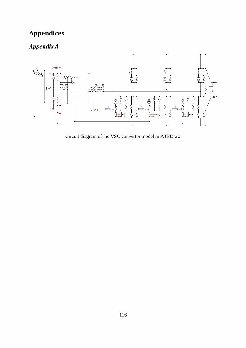
116
Appendices
Appendix A
Circuit diagram of the VSC convertor model in ATPDraw
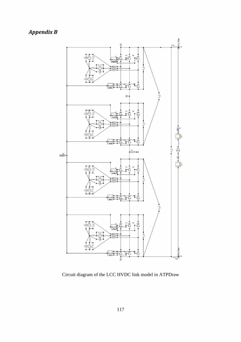
117
Appendix B
Circuit diagram of the LCC HVDC link model in ATPDraw

118
Appendix C
Circuit diagram of the model of SF6 switchgear with two interrupters in ATPDraw

119
Appendix D
The programme code for calculation of the arc resistance in the SF6 AT interrupter:
MODEL DIEL -- 250 kV, T-Art INPUT I, U DATA TOPEN OUTPUT RES VAR RES Gmayr -- Mayr's conductance e S P0 TAU -- time constant X HISTORY I, Gmayr, U, RES INIT RES:=0 Gmayr:=1000 e:=0 S:=0 P0:=0 TAU:=0 X:=0 ENDINIT EXEC IF t>=TOPEN THEN IF t<Topen+0.002 THEN e:=25*(t-Topen) ENDIF IF t>=Topen+0.002 AND t<Topen+0.008 THEN e:=125*(t- Topen)-0.2 ENDIF IF t>=Topen+0.008 AND t<Topen+0.01 THEN e:=100*(t-T open) ENDIF IF t>=Topen+0.01 AND t<Topen+0.024 THEN e:=1 ENDIF IF t>=Topen+0.024 AND t<Topen+0.027 THEN e:=-850*(t -Topen)/3+7.8 ENDIF IF t>=Topen+0.027 AND t<Topen+0.05-200*timestep THE N e:=-150*(t-Topen)/23+15/46 ENDIF IF ABS(I)<=50 THEN P0:= 64900 ELSE P0:=150000+800000*Gmayr**0.35+ABS(I)*625 ENDIF TAU:=0.00000022+0.00000022*Gmayr**0.15

120
S:=I*I/TAU/P0 diffeq((1/TAU)|d0+1|d1)|GmayrDMIN:0.00000000000000 0001 := S RES:=1/Gmayr*e ELSE RES:=0.000001 ENDIF
ENDEXEC
ENDMODEL


![High voltage circuit breakers. - EnergoBos voltage circuit breakers. Mirsad Kapetanovic High voltage circuit breakers. Mirsad Kapetanovic KE_boek [omslag2010]_15.indd 1 09 …Published](https://img.pdfslide.net/doc/110x75/5b394b5e7f8b9a4a728e0833/high-voltage-circuit-breakers-voltage-circuit-breakers-mirsad-kapetanovic-high.jpg)