Embed Size (px)
Citation preview

Binary Systems Page 1
Condensed Notes
On
Digital Logics (According to BScCSIT syllabus TU)
By Bishnu Rawal
csitn
epal
By Bishnu Rawal

Binary Systems Page 2
Unit 1
Binary Systems
Introduction We are in “Information age” since digital systems have such a prominent and growing role in modern society. They are involved in our business transactions, communications, transportation, medical treatment and entertainment. In industrial world they are heavily employed in design, manufacturing, distribution and sales.
Analog System Analog systems process analog signals (continuous time signals) which can take any value within a range, for example the output from a speaker or a microphone.
Digital System
Digital systems process digital signals which can take only a limited number of values (discrete steps), usually just two values are used: the positive supply voltage (+Vs) and zero volts (0V).
Digital systems contain devices such as logic gates, flip-flops, shift registers and counters.
The general purpose digital computer is a best known example of digital system.
Generic Digital computer structure
Fig: Block diagram of digital computer
An analog meter can display any value within the range available on its scale.
However, the precision of readings is limited by our ability to read them. E.g.
meter on the right shows 1.25V because the pointer is estimated to be half way
between 1.2 and 1.3. The analogue meter can show any value between 1.2 and
1.3 but we are unable to read the scale more precisely than about half a division.
A digital meter can display many values, but not every value within its range. For
example the display on the right can show 6.25 and 6.26 but not a value between
them. This is not a problem because digital meters normally have sufficient digits
to show values more precisely than it is possible to read an analogue display.
Actually processor contains 4
functional modules: CPU,
FPU, MMU and internal
cache.
Here only CPU is specified.
csitn
epal
By Bishnu Rawal

Binary Systems Page 3
Working principle of generic digital computer: Memory stores programs as well as input, output and intermediate data. The datapath performs arithmetic and other data-processing operations as specified by the program. The control unit supervises the flow of information between the various units. A datapath, when combined with the control unit, forms a component referred to as a central processing unit, or CPU. The program and data prepared by the user are transferred into memory by means of an input device such as a keyboard. An output device, such as a CRT (cathode-ray tube) monitor, displays the results of the computations and presents them to the user. Advantages of digital system: Have made possible many scientific, industrial, and commercial advances that would have been
unattainable otherwise. Less expensive
More reliable
Easy to manipulate
Flexibility and Compatibility
Information storage can be easier in digital computer systems than in analog ones. New features
can often be added to a digital system more easily too.
Disadvantages of digital system: Use more energy than analog circuits to accomplish the same tasks, thus producing more heat
as well. Digital circuits are often fragile, in that if a single piece of digital data is lost or misinterpreted,
the meaning of large blocks of related data can completely change. Digital computer manipulates discrete elements of information by means of a binary code. Quantization error during analog signal sampling.
Information Representation Signals Information variables represented by physical quantities. For digital systems, the variables take on discrete values. Two level or binary values are the most prevalent values in digital systems. Binary values are represented abstractly by:
• digits 0 and 1 • words (symbols) False (F) and True (T) • words (symbols) Low (L) and High (H) • and words On and Off.
Binary values are represented by values or ranges of values of physical quantities Signal Examples over time
csitn
epal
By Bishnu Rawal

Binary Systems Page 4
Here is an example waveform of a quantized signal. Notice how the magnitude of the wave can only take certain values, and that creates a step-like appearance. This image is discrete in magnitude, but is continuous in time (asynchronous):
Signal Example – physical quantity: Voltage
What are other physical quantities representing 0 and 1?
1. CPU: Voltage • Disk: Magnetic Field Direction 2. CD: Surface Pits/Light • Dynamic RAM: Electrical Charge
Number Systems Here we discuss positional number systems with Positive radix (or base) r. A number with radix r is represented by a string of digits as below i.e. wherever you guys see numbers of whatever bases, all numbers can be written in general as:
An-1 An-2 … A1 A0 . A-1 A-2 … A-m + 1 A-m Most Significant Digit (MSD) Least Significant Digit (LSD) Integer portion (n digits) Fractional portion (m digits) in which 0 ≤ Ai < r (since each being a symbol for particular base system viz. for r = 10 (decimal number system) Ai will be one of 0,1,2,…,8,9). Subscript i gives the position of the coefficient and, hence, the weight ri by which the coefficient must be multiplied. HEY! Confused? Don’t worry! I will describe specific number systems (r=2, 8, 10 and 16) used in digital computers later one by one, then the concept will be quite clear.
Radix point
csitn
epal
By Bishnu Rawal

Binary Systems Page 5
In general, a number in base r contains r digits, 0, l, 2... r- 1, and is expressed as a power series in r with the general form:
(Number)r = An-1 rn-1 + An-2 r
n-2 + … + A1 r1 + A0 r0 + A-1 r
-1 + A-2 r-2 + … + A-m+1 r
-m+1 + A-m r-m
Decimal Number System (Base-10 system) Radix (r) = 10 Symbols = 0 through r-1 = 0 through 10-1 = {0, 1, 2... 8, 9} I am starting from base-10 system since it is used vastly in everyday arithmetic besides computers to represent numbers by strings of digits or symbols defined above, possibly with a decimal point. Depending on its position in the string, each digit has an associated value of an integer raised to the power of 10. Example: decimal number 724.5 is interpreted to represent 7 hundreds plus 2 tens plus 4 units plus 5 tenths. 724.5 = 7 X 10² + 2 X 101 + 4 X 100 +5 X 10⁻¹
Binary Number System (Base-2 system) Radix (r) = 2 Symbols = 0 through r-1 = 0 through 2-1 = {0, 1} A binary numbers are expressed with a string of 1'sand 0's and, possibly, a binary point within it. The decimal equivalent of a binary number can be found by expanding the number into a power series with a base of 2. Example: (11010.01)2 can be interpreted using power series as: (11010.01)2 = 1 X 24 + 1 X 23 + 0 X 22 + 1 X 21 + 0 X 20 +0 X 2-1 + 1 X 2-2 = (26.25)10
Digits in a binary number are called bits (Binary digITs). When a bit is equal to 0, it does not contribute to the sum during the conversion. Therefore, the conversion to decimal can be obtained by adding the numbers with powers of 2 corresponding to the bits that are equal to 1. Looking at above example, (11010.01)2 = 16 + 8 + 2 + 0.25 = (26.25)10 .
Table: Numbers obtained from 2 to the power of n
Octal Number System (Base-8 system) Radix (r) = 8 Symbols = 0 through r-1 = 0 through 8-1 = {0, 1, 2…6, 7}
In computer work,
210 is referred to as K (kilo),
220 as M (mega),
230 as G (giga),
240 as T (tera) and so on.
csitn
epal
By Bishnu Rawal

Binary Systems Page 6
An octal numbers are expressed with a strings of symbols defined above, possibly, an octal point within it. The decimal equivalent of a octal number can be found by expanding the number into a power series with a base of 8. Example: (40712.56)8 can be interpreted using power series as: (40712.56)8 = 4 X 84 + 0 X 83 + 7 X 82 + 1 X 81 + 2 X 80 + 5 X 8-1 + 6 X 8-2 = (16842.1)10
Hexadecimal Number System (Base-16 system) Radix (r) = 16 Symbols = 0 through r-1 = 0 through 16-1 = {0, 1, 2…9, A, B, C, D, E, F} A hexadecimal numbers are expressed with a strings of symbols defined above, possibly, a hexadecimal point with in it. The decimal equivalent of a hexadecimal number can be found by expanding the number into a power series with a base of 16. Example: (4D71B.C6)16 can be interpreted using power series as: (4D71B.C6)16 = 4 X 164 + D X 163 + 7 X 162 + 1 X 161 + B X 160 + C X 16-1 + 6 X 16-2 = 4 X 164 + 13 X 163 + 7 X 162 + 1 X 161 + 11 X 160 + 12 X 16-1 + 6 X 16-2
= (317211.7734375)10
Number Base Conversions Case I: Base-r system to Decimal: Base-r system can be binary (r=2), octal (r=8), hexadecimal (r=16), base-60 system or any other. For decimal system as destination of conversion, we just use power series explained above with varying r and sum the result according to the arithmetic rules of base-10 system. I have already done examples for binary to decimal, octal to decimal and hexadecimal to decimal. For refreshment lets assume base-1000 number (458HQY)1000. Where n = 6 and m = 0. (458HQY)1000 = An-1 r
n-1 + An-2 rn-2 + … + A1 r
1 + A0 r0 + A-1 r-1 + A-2 r
-2 + … + A-m+1 r-m+1 + A-m r-m
= 4 X 10005 + 5 X 10004 + 8 X 10003 + H X 10002 + Q X 10001 + Y X 10000
=Resulting number will be in decimal. Here I have supposed various symbols for base-1000 system. Don’t worry, if someone gives you base-1000 number for conversion, he should also define all 1000 symbols (0-999). Case II: Decimal to Base-r system: Conversion follows following algorithm.
1. Separate the number into integer and fraction parts if radix point is given. 2. Divide “Decimal Integer part” by base r repeatedly until quotient becomes zero and storing
remainders at each step. 3. Multiply “Decimal Fraction part” successively by r and accumulate the integer digits so
obtained. 4. Combine both accumulated results and parenthesize the whole result with subscript r.
Example I: Decimal to binary
(41.6875)10 = (?)2 Here Integer part = 41 and fractional part = 0.6875
csitn
epal
By Bishnu Rawal

Binary Systems Page 7
Example II: Decimal to octal
(153.45)10 = (?)8 Here integer part = 153 and fractional part = 0.45
153 0.45 19 1 X 8 2 3 ----------------
0 2 3.60 X 8
(153)10 = (231)8 ---------------- 4.80 X 8 ---------------- 6.40 (may not end, choice
is upon you to end up) (0.45)10 = (346)8
(153.45)10 = (231.346)8
Example III: Decimal to Hexadecimal
(1459.43)10 = (?)16 Here integer part = 1459 and fractional part = 0.43
1459 0.43 91 4 X16
5 11 (=B) ---------------- 0 5 6.80
X16 (1459)10 = (5B4)16 ---------------- 12.80 X16 ---------------- 12.80 (Never ending…) (0.43)10 = (6CC)8
(1459.43)10 = (5B4.6CC)16
Multiply always
the portion after
radix point.
This is simply division by 8, I am writing Quotients and remainders only.
csitn
epal
By Bishnu Rawal

Binary Systems Page 8
Case III: Binary to octal & hexadecimal and vice-versa: Conversion from and to binary, octal and hexadecimal representation plays an important part in digital computers. Since,
23 = 8, octal digit can be represented by at least 3 binary digits. (We have discussed this much better in class). So to convert given binary number into its equivalent octal, we divide it into groups of 3 bits, give each group an octal symbol and combine the result.
o Integer part: Group bits from right to left of an octal point. 0’s can be added to make it multiple of 3 (not compulsory).
o Fractional part: Group bits from left to right of an octal point. 0’s must be added to if bits are not multiple of 3 (Note it).
24 = 16, each hex digit corresponds to 4 bits. So to convert given binary number into its equivalent hex, we divide it into groups of 4 bits, give each group a hex digit and combine the result. If hex point is given, then process is similar as of octal.
15 numbers in 4 systems summarized below for easy reference.
Example:
1. Binary to octal: (10110001101011.11110000011)2 = (010 110 001 101 011. 111 100 000 110)2 = (26153.7406)8 2 6 1 5 3 7 4 0 6
2. Binary to hexadecimal: (10110001101011.11110000011)2 = (0010 1100 0110 1011. 1111 0000 0110)2 = (2C6B.F06)16 2 C 6 B F 0 6
3. From hex & octal to binary is quite easy, we just need to remember the binary of particular hex or octal digit. (673.12)8 = 110 111 011. 001 010 = (110111011.00101)2 (3A6.C)16 = 0011 1010 0110. 1100 = (1110100110.11)2
csitn
epal
By Bishnu Rawal

Binary Systems Page 9
Complements
Complements are used in digital computers for simplifying the subtraction operation and for logical manipulation. There are two types of complements for each base-r system: r's complement and the second as the (r - 1)'s complement. When the value of the base r is substituted, the two types are referred to as the 2's complement and 1's complement for binary numbers, the 10's complement and 9's complement for decimal numbers etc.
Subtraction with complements
The direct method of subtraction taught in elementary schools uses the borrow concept. When subtraction is implemented with digital hardware, this method is found to be less efficient than the method that uses complements. The subtraction of two n-digit unsigned numbers M - N in base-r can be done as follows:
1. Add the minuend M to the r's complement of the subtrahend N. This performs M + (rn –N) = M -N + r".
2. If M >= N, the sum will produce an end carry, r", which is discarded; what is left is the result M - N.
3. If M < N, the sum does not produce an end carry and is equal to rn - (N - M), which is the r's complement of (N - M). To obtain the answer in a familiar form, take the r's complement of the sum and place a negative sign in front.
Example I:
(r-1)'s Complement (diminished radix compl.) (r-1)'s complement of a number N is defined as (rn -1) –N Where N is the given number
r is the base of number system n is the number of digits in the given number
To get the (r-1)'s complement fast, subtract each digit of a number from (r-1). Example:
- 9's complement of 83510 is 16410 (Rule: (10n -1) –N)
- 1's complement of 10102 is 01012 (bit by bit complement operation)
r's Complement (radix complement) r's complement of a number N is defined as rn –N Where N is the given number r is the base of number system
n is the number of digits in the given number
To get the r's complement fast, add 1 to the low-order digit of its (r-1)'s complement. Example:
- 10's complement of 83510 is 16410 + 1 = 16510
- 2's complement of 10102 is 01012 + 1 = 01102
HEY! M has 5 digits and N has only 4 digits. Both numbers must have the same number of digits; so we can write N as 03250. Taking the 10's complement of N produces a 9 in the most significant position. The occurrence of the end carry signifies that M >= N and the result is positive.
csitn
epal
By Bishnu Rawal

Binary Systems Page 10
Example II:
Example III:
Example IV: Repeating Example III using 1’s complement.
csitn
epal
By Bishnu Rawal

Binary Systems Page 11
Binary Codes Electronic digital systems use signals that have two distinct values and circuit elements that have two stable states. There is a direct analogy among binary signals, binary circuit elements, and binary digits. A binary number of n digits, for example, may be represented by n binary circuit elements, each having an output signal equivalent to a 0 or a 1. Digital systems represent and manipulate not only binary numbers, but also many other discrete elements of information. Any discrete element of information distinct among a group of quantities can be represented by a binary code. Binary codes play an important role in digital computers. The codes must be in binary because computers can only hold 1's and 0's.
1. Binary Coded Decimal (BCD) The binary number system is the most natural system for a computer, but people are accustomed to the decimal system. So, to resolve this difference, computer uses decimals in coded form which the hardware understands. A binary code that distinguishes among 10 elements of decimal digits must contain at least four bits. Numerous different binary codes can be obtained by arranging four bits into 10 distinct combinations. The code most commonly used for the decimal digits is the straightforward binary assignment listed in the table below. This is called binary-coded decimal and is commonly referred to as BCD.
Table: 4-bit BCD code for decimal digits
2. Error-Detection codes Binary information can be transmitted from one location to another by electric wires or other communication medium. Any external noise introduced into the physical communication medium may change some of the bits from 0 to 1 or vice versa. The purpose of an error-detection code is to detect such bit-reversal errors. One of the most common ways to achieve error detection is by means of a parity bit. A parity bit is the extra bit included to make the total number of 1's in the resulting code word either even or odd. A message of 4-bits and a parity bit P are shown in the table below:
A number with n decimal digits will require 4n bits in BCD. E.g. decimal 396 is represented in BCD with 12 bits as 0011 1001 0110.
Numbers greater than 9 has a representation different from its equivalent binary number, even though both contain 1's and 0's.
Binary combinations 1010 through 1111 are not used and have no meaning in the BCD code.
Example: (185)10 = (0001 1000 0101)BCD = (10111001)2
csitn
epal
By Bishnu Rawal

Binary Systems Page 12
3. Gray code (Reflected code) It is a binary coding scheme used to represent digits generated from a mechanical sensor that may be prone to error. Used in telegraphy in the late 1800s, and also known as "reflected binary code”. Gray code was patented by Bell Labs researcher Frank Gray in 1947. In Gray code, there is only one bit location different between two successive values, which makes mechanical transitions from one digit to the next less error prone. The following chart shows normal binary representations from 0 to 15 and the corresponding Gray code.
Decimal digit Binary code Gray code 0 0000 0000 1 0001 0001
2 0010 0011 3 0011 0010
4 0100 0110 5 0101 0111 6 0110 0101 7 0111 0100 8 1000 1100 9 1001 1101 10 1010 1111
11 1011 1110 12 1100 1010 13 1101 1011 14 1110 1001 15 1111 1000
The Gray code is used in applications where the normal sequence of binary numbers may produce an error or ambiguity during the transition from one number to the next. If binary numbers are used, a change from 0111 to 1000 may produce an intermediate erroneous number 1001 if the rightmost bit takes more time to change than the other three bits. The Gray code eliminates this problem since only one bit changes in value during any transition between two numbers.
Error Checking Mechanism:
During the transmission of information from one location to another, an even parity bit is generated in the sending end for each message transmission. The message, together with the parity bit, is transmitted to its destination. The parity of the received data is checked in the receiving end. If the parity of the received information is not even, it means that at least one bit has changed value during the transmission. This method detects one, three, or any odd combination of errors in each message that is transmitted. An even combination of errors is undetected. Additional error-detection schemes may be needed to take care of an even combination of errors.
csitn
epal
By Bishnu Rawal

Binary Systems Page 13
4. Alphanumeric codes Alphanumeric character set is a set of elements that includes the 10 decimal digits, 26 letters of the alphabet and special characters such as $, %, + etc. It is necessary to formulate a binary code for this set to handle different data types. If only capital letters are included, we need a binary code of at least six bits, and if both uppercase letters and lowercase letters are included, we need a binary code of at least seven bits.
ASCII character code
The standard binary code for the alphanumeric characters is called ASCII (American Standard Code for Information Interchange). It uses seven bits to code 128 characters as shown in the table below. The seven bits of the code are designated by B1 through B7 with B7 being the most significant bit.
Various control character symbolic notation stands for:
Example: ASCII for each symbol is (B7B6B5B4B3B2B1) G 100 0111, ( 010 1000, h 110 1000, > 011 1110 and so on.
NOTE:
Decimal digits
in ASCII can be
converted to
BCD by
removing the
three higher
order bits,
011.
csitn
epal
By Bishnu Rawal

Binary Systems Page 14
EBCDIC character code EBCDIC (Extended Binary Coded Decimal Interchange Code) is another alphanumeric code used in IBM equipment. It uses eight bits for each character. EBCDIC has the same character symbols as ASCII, but the bit assignment for characters is different. As the name implies, the binary code for the letters and numerals is an extension of the binary-coded decimal (BCD) code. This means that the last four bits of the code range from 0000 though 1001 as in BCD.
Integrated Circuits (ICs)
An Integrated circuit is an association (or connection) of various electronic devices such as resistors, capacitors and transistors etched (or fabricated) to a semiconductor material such as silicon or germanium. It is also called as a chip or microchip. An IC can function as an amplifier, rectifier, oscillator, counter, timer and memory. Sometime ICs are connected to various other systems to perform complex functions.
Types of ICs ICs can be categorized into two types
Analog or Linear ICs Digital or logic ICs
Further there are certain ICs which can perform as a combination of both analog and digital functions. Analog or Linear ICs: They produce continuous output depending on the input signal. From the name of the IC we can deduce that the output is a linear function of the input signal. Op-amp (operational amplifier) is one of the types of linear ICs which are used in amplifiers, timers and counters, oscillators etc. Digital or Logic ICs: Unlike Analog ICs, Digital ICs never give a continuous output signal. Instead it operates only during defined states. Digital ICs are used mostly in microprocessor and various memory applications. Logic gates are the building blocks of Digital ICs which operate either at 0 or 1.
Advantages of ICs In consumer electronics, ICs have made possible the development of many new products,
including personal calculators and computers, digital watches, and video games.
They have also been used to improve or lower the cost of many existing products, such as appliances, televisions, radios, and high-fidelity equipment.
The logic and arithmetic functions of a small computer can now be performed on a single VLSI chip called a microprocessor.
Complete logic, arithmetic, and memory functions of a small computer can be packaged on a single printed circuit board, or even on a single chip.
Levels of Integration During 1959 two different scientists invented IC’s. Jack Kilby from Texas Instruments made his first germanium IC during 1959 and Robert Noyce made his first silicon IC during the same year. But ICs were not the same since the day of their invention; they have evolved a long way. Integrated circuits are often classified by the number of transistors and other electronic components they contain:
SSI (small-scale integration): Up to 100 electronic components per chip MSI (medium-scale integration): From 100 to 3,000 electronic components per chip
csitn
epal
By Bishnu Rawal

Binary Systems Page 15
LSI (large-scale integration): From 3,000 to 100,000 electronic components per chip VLSI (very large-scale integration): From 100,000 to 1,000,000 electronic components per chip ULSI (ultra large-scale integration): More than 1 million electronic components per chip
SIP (Single In-line Package) and DIP (Dual In-line Package) SIP A single in-line package is an electronic device package which has one row of connecting pins. It is not as popular as the dual in-line package (DIP) which contains two rows of pins, but has been used for packaging RAM chips and multiple resistors with a common pin. SIPs group RAM chips together on a small board. The board itself has a single row of pin-leads that resembles a comb extending from its bottom edge, which plug into a special socket on a system or system-expansion board. SIPs are commonly found in memory modules. SIP is not to be confused with SIPP which is an archaic term referring to Single In-line Pin Package which was a memory used in early computers.
DIP Dual in-line package (DIP) is a type of semiconductor component packaging. DIPs can be installed either in sockets or permanently soldered into holes extending into the surface of the printed circuit board. DIP is relatively broadly defined as any rectangular package with two uniformly spaced parallel rows of pins pointing downward, whether it contains an IC chip or some other device(s), and whether the pins emerge from the sides of the package and bend downwards. A DIP is usually referred to as a DIPn, where n is the total number of pins. For example, a microcircuit package with two rows of seven vertical leads would be a DIP14. The photograph below shows three DIP14 ICs.
Several DIP variants for ICs exist, mostly distinguished by packaging material:
Ceramic Dual In-line Package (CERDIP or CDIP) Plastic Dual In-line Package (PDIP) Shrink Plastic Dual In-line Package (SPDIP) -A denser version of the PDIP with a 0.07 in.
(1.778 mm) lead pitch. Skinny Dual In-line Package (SDIP) – Sometimes used to refer to a 0.3 in. wide DIP, normally
when clarification is needed e.g. for a 24 or 28 pin DIP.
csitn
epal
By Bishnu Rawal

Binary Systems Page 16
Fig: Several PDIPs and CERDIPs. The large CERDIP in the foreground is an Intel 8080
microprocessor.
SIMM (Single In-line Memory Module) and DIMM (Dual In-line Memory Module) Theses two terms (SIMM and DIMM) refer to a way series of dynamic random access memory integrated circuits modules are mounted on a printed circuit board and designed for use in personal computers, workstations and servers. SIMM Short for Single In-line Memory Module, SIMM is a circuit board that holds six to nine memory chips per board, the ninth chip usually an error checking chip (parity/non parity) and were commonly used with Intel Pentium or Pentium compatible motherboards. SIMMs are rarely used today and have been widely replaced by DIMMs. SIMMs are available in two flavors: 30 pin and 72 pin. 30-pin SIMMs are the older standard, and were popular on third and fourth generation motherboards. 72-pin SIMMs are used on fourth, fifth and sixth generation PCs.
` DIMM Short for Dual In-line Memory Module, DIMM is a circuit board that holds memory chips. DIMMs have a 64-bit path because of the Pentium Processor requirements. Because of the new bit path, DIMMs can be installed one at a time, unlike SIMMs on a Pentium that would require two to be added. Below is an example image of a 512MB DIMM memory stick.
csitn
epal
By Bishnu Rawal

Binary Systems Page 17
SO-DIMM is short for Small Outline DIMM and is available as a 72-pin and 144-pin configuration. SO-DIMMs are commonly utilized in laptop computers. Some of the advantages DIMMs have over SIMMs:
DIMMs have separate contacts on each side of the board, thereby providing twice as much data as a single SIMM.
The command address and control signals are buffered on the DIMMs. With heavy memory requirements this will reduce the loading effort of the memory.
Description of a few types of chips (Just for Knowledge, not in syllabus) CMOS: in computer science, acronym for complementary metal-oxide semiconductor. A semiconductor device that consists of two metal-oxide semiconductor field effect transistors (MOSFETs), one N-type and one P-type, integrated on a single silicon chip. Generally used for RAM and switching applications, these devices have very high speed and extremely low power consumption. They are, however, easily damaged by static electricity. Digital Signal Processor (DSP): An integrated circuit designed for high-speed data manipulations, used in audio, communications, image manipulation, and other data-acquisition and data-control applications. Dynamic RAM (DRAM): In computer science, a form of semiconductor random access memory (RAM). Dynamic RAMs store information in integrated circuits that contain capacitors. Because capacitors lose their charge over time, dynamic RAM boards must include logic to "refresh" (recharge) the RAM chips continuously. While a dynamic RAM is being refreshed, it cannot be read by the processor; if the processor must read the RAM while it is being refreshed, one or more wait states occur. Because their internal circuitry is simple, dynamic RAMs are more commonly used than static RAMs, even though they are slower. A dynamic RAM can hold approximately four times as much data as a static RAM chip of the same complexity. EPROM: In computer science, acronym for erasable programmable read-only memory, also called reprogrammable read-only memory (RPROM). EPROMs are nonvolatile memory chips that are programmed after they are manufactured. EPROMs are a good way for hardware vendors to put variable or constantly changing code into a prototype system when the cost of producing many PROM chips would be prohibitive. EPROMs differ from PROMs in that they can be erased, generally by removing a protective cover from the top of the chip package and exposing the semiconductor material to ultraviolet light, and can be reprogrammed after having been erased. Although EPROMs are more expensive than PROMs, they can be more cost-effective in the long run if many changes are needed. PROM: Acronym for programmable read-only memory. In computer science, a type of read-only memory (ROM) that allows data to be written into the device with hardware called a PROM programmer. After a PROM has been programmed, it is dedicated to that data, and it cannot be
csitn
epal
By Bishnu Rawal

Binary Systems Page 18
reprogrammed. Because ROMs are cost-effective only when produced in large volumes, PROMs are used during the prototyping stage of the design. New PROMs can be created and discarded as needed until the design is perfected. Reduced Instruction Set Computer (RISC): Type of microprocessor that focuses on rapid and efficient processing of a relatively small set of instructions. RISC design is based on the premise that most of the instructions a computer decodes and executes are simple. As a result, RISC architecture limits the number of instructions that are built into the microprocessor but optimizes each so it can be carried out very rapidly-usually within a single clock cycle. RISC chips thus execute simple instructions faster than microprocessors designed to handle a much wider array of instructions. ROM: Acronym for read-only memory. In computer science, semiconductor-based memory that contains instructions or data that can be read but not modified. To create a ROM chip, the designer supplies a semiconductor manufacturer with the instructions or data to be stored; the manufacturer then produces one or more chips containing those instructions or data. Because creating ROM chips involves a manufacturing process, it is economically viable only if the ROM chips are produced in large quantities; experimental designs or small volumes are best handled using PROM or EPROM. In general usage, the term ROM often means any read-only device, including PROM and EPROM. Static RAM (SRAM): In computer science, a form of semiconductor memory (RAM). Static RAM storage is based on the logic circuit known as a flip-flop, which retains the information stored in it as long as there is enough power to run the device. A static RAM chip can store only about one-fourth as much data as a dynamic RAM chip of the same complexity, but static RAM does not require refreshing and is usually much faster than dynamic RAM. It is also more expensive. Static RAMs are usually reserved for use in caches.
csitn
epal
By Bishnu Rawal
Boolean Algebra and Logic Gates Page 1
Unit 2
Boolean algebra and Logic Gates
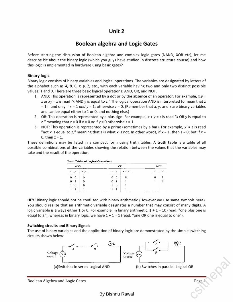
Before starting the discussion of Boolean algebra and complex logic gates (NAND, XOR etc), let me describe bit about the binary logic (which you guys have studied in discrete structure course) and how this logic is implemented in hardware using basic gates?
Binary logic Binary logic consists of binary variables and logical operations. The variables are designated by letters of the alphabet such as A, B, C, x, y, Z, etc., with each variable having two and only two distinct possible values: 1 and 0. There are three basic logical operations: AND, OR, and NOT.
1. AND: This operation is represented by a dot or by the absence of an operator. For example, x.y = z or xy = z is read "x AND y is equal to z." The logical operation AND is interpreted to mean that z = 1 if and only if x = 1 and y = 1; otherwise z = 0. (Remember that x, y, and z are binary variables and can be equal either to 1 or 0, and nothing else.)
2. OR: This operation is represented by a plus sign. For example, x + y = z is read "x OR y is equal to z," meaning that z = 0 if x = 0 or if y = 0 otherwise z = 1.
3. NOT: This operation is represented by a prime (sometimes by a bar). For example, x' = z is read "not x is equal to z," meaning that z is what x is not. In other words, if x = 1, then z = 0; but if x = 0, then z = 1.
These definitions may be listed in a compact form using truth tables. A truth table is a table of all possible combinations of the variables showing the relation between the values that the variables may take and the result of the operation.
HEY! Binary logic should not be confused with binary arithmetic (However we use same symbols here). You should realize that an arithmetic variable designates a number that may consist of many digits. A logic variable is always either 1 or 0. For example, in binary arithmetic, 1 + 1 = 10 (read: "one plus one is equal to 2"), whereas in binary logic, we have 1 + 1 = 1 (read: "one OR one is equal to one"). Switching circuits and Binary Signals The use of binary variables and the application of binary logic are demonstrated by the simple switching circuits shown below:
(a)Switches in series-Logical AND (b) Switches in parallel-Logical OR
csitn
epal
By Bishnu Rawal

Boolean Algebra and Logic Gates Page 2
Let the manual switches A and B represent two binary variables with values equal to 0 when the switch is open and 1 when the switch is closed. Similarly, let the lamp L represent a third binary variable equal to 1 when the light is on and 0 when off. Electronic digital circuits are sometimes called switching circuits because they behave like a switch, with the active element such as a transistor either conducting (switch closed) or not conducting (switch open). Instead of changing the switch manually, an electronic switching circuit uses binary signals to control the conduction or non-conduction state of the transistor.
Basic Logic Gates (Digital logic gates will be covered in detail later) Logic gates are electronic circuits that operate on one or more input signals to produce an output signal. Electrical signals such as voltages or currents exist throughout a digital system in either one of two recognizable values (bi-state 0 or 1). Voltage-operated circuits respond to two separate voltage ranges (Example of voltage ranges is discussed in unit 1) that represent a binary variable equal to logic 1 or logic 0. The graphics symbols used to designate the three types of gates AND, OR, and NOT are shown in Figure below:
(a) Graphic symbols
(b) Timing diagram
These circuits, called gates, are blocks of hardware that produce a logic-1 or logic-0 output signal if input logic requirements are satisfied.
Note that four different names have been used for the same type of circuits: digital circuits, switching circuits, logic circuits, and gates.
AND and OR gates may have more than two inputs.
NOT gate is single input circuit, it simply inverts the input.
The two input signals X and Y to the AND and OR gates take on one of four possible combinations: 00, 01, 10, or 11. These input signals are shown as timing diagrams, together with the timing diagrams for the corresponding output signal for each type of gate. The horizontal axis of a timing diagram represents time, and the vertical axis shows a signal as it changes between the two possible voltage levels. The low level represents logic 0 and the high level represents logic I. 1l1e AND gate responds with a logic-1 output signal when both input signals are logic-1. The OR gate responds with a logic-1 output signal if either input signal is logic-1.
csitn
epal
By Bishnu Rawal

Boolean Algebra and Logic Gates Page 3
Boolean algebra In 1854 George Boole introduced a systematic treatment of logic and developed for this purpose an algebraic system now called Boolean algebra. In 1938 C. E. Shannon introduced a two-valued Boolean algebra called switching algebra, in which he demonstrated that the properties of bistable electrical switching circuits can be represented by this algebra. Thus, the mathematical system of binary logic is known as Boolean or switching algebra. This algebra is conveniently used to describe the operation of complex networks of digital circuits. Designers of digital systems use Boolean algebra to transform circuit diagrams to algebraic expressions and vice versa. For any given algebra system, there are some initial assumptions, or postulates, that the system follows. We can deduce additional rules, theorems, and other properties of the system from this basic set of postulates. Boolean algebra systems often employ the postulates formulated by E. V. Huntington in 1904.
Postulates Boolean algebra is an algebraic structure defined on a set of elements B (Boolean system) together with two binary operators + (OR) and • (AND) and unary operator ' (NOT), provided the following postulates are satisfied:
P1 Closure: Boolean algebra is closed under the AND, OR, and NOT operations. P2 Commutativity: The • and + operators are commutative i.e. x + y = y + x and x • y = y • x, for all x, y ∈ B. P3 Distribution: • and + are distributive with respect to one another i.e.
X • (y + z) = (x • y) + (x • z).
x + (y • z) = (x + y) • (x + z), for all x, y, z ∈ B. P4 Identity: The identity element with respect to • is 1 and + is 0 i.e. x + 0 = 0 + x = x and x • 1=1• x = x. There is no identity element with respect to logical NOT. P5 Inverse: For every value x there exists a value x' such that x • x' = 0 and x + x' = 1. This value is the logical complement (or NOT) of x. P6 There exists at least two elements x, y ∈ B such that x ≠ y.
One can formulate many Boolean algebras (viz. set theory, n-bit vectors algebra), depending on the choice of elements of B and the rules of operation. Here, we deal only with a two-valued Boolean algebra, i.e., B = {0, 1}. Two-valued Boolean algebra has applications in set theory and in propositional logic. Our interest here is with the application of Boolean algebra to gate-type circuits.
Basic theorems and Properties of Boolean algebra Duality Postulates of Boolean algebra are found in pairs; one part may be obtained from the other if the binary operators and the identity elements are interchanged. This important property of Boolean algebra is called the duality principle. It states that “Every algebraic expression deducible from the postulates of Boolean algebra remains valid if the operators and identity elements are interchanged”. In a two-valued Boolean algebra, the identity elements and the elements of the set B are the same: 1 and 0. If the dual of an algebraic expression is desired, we simply interchange OR and AND operators and replace 1's by 0's and 0's by 1's.
csitn
epal
By Bishnu Rawal

Boolean Algebra and Logic Gates Page 4
Basic theorems The theorems, like the postulates, are listed in pairs; each relation is the dual of the one paired with it. The postulates are basic axioms of the algebraic structure and need no proof. The theorems must be proven from the postulates. six theorems of Boolean algebra are given below: Theorem1: Idempotence (a) x + x = x (b) x.x = x Theorem2: Existence: 0&1 (a) x + 1 = 1 (b) x.0 = 0 Theorem3: Involution (x')' = x Theorem4: Associative (a) x + (y + z) = (x + y) + z (b) x(yz) = (xy)z Theorem5: Demorgan (a) (x + y)' = x'y' (b) (xy)' = x' + y' Theorem6: Absorption (a) x + xy = x (b) x(x + y) = x Proofs: (a) The proofs of the theorems with one variable are presented below:
THEOREM 1(a): x + x = x
x + x = (x + x) . 1 (P4: Identity element) = (x + x)(x + x') (P5: Existence of inverse) = x + xx' (P3: Distribution) =x + 0 (P5: Existence of inverse) =x (P4: Identity element)
THEOREM 1(b): x·x = x x.x = xx + 0 (P4: Identity element)
=xx + xx' (P5: Existence of inverse) =x(x + x') (P3: Distribution) = x.1 (P5: Existence of inverse) =x (P4: Identity element)
Hey! Each step in theorem 1(b) and 1(a) are dual of each other. THEOREM 2(a): x + 1 = 1
x + 1 = 1· (x + 1) (P4: Identity element) = (x + x')(x + 1) (P5: Existence of inverse) =x + x'·1 (P3: Distribution) = x + x' (P4: Identity element) = 1 (P5: Existence of inverse)
THEOREM 2(b): x.0 = 0 by duality. THEOREM 3: (x ')' = x. From P5, we have x + x' = 1 and x.x' = 0, which defines the complement of x. The complement of x' is x and is also (x')'. Therefore, since the complement is unique, we have that (x')' = x. (b) The theorems involving two or three variables may be proven algebraically from the postulates and
the theorems that have already been proven. For example, lets prove Demorgan’s theorem: THEOREM 5(a): (x + y)' = x'y' From postulate P5 (Existence of inverse), for every x in a Boolean algebra there is a unique x' such that
x + x' = 1 and x • x' = 0
One variable theorems
2 or 3 variable theorems
csitn
epal
By Bishnu Rawal

Boolean Algebra and Logic Gates Page 5
So it is sufficient to show that x'y' is the complement of x + y. We'll do this by showing that (x + y) + (x'y') = 1 and (x + y) • (x'y') = 0. (x + y) + (x'y') = [(x + y) + x'] [(x + y) + y'] [OR distributes over AND (P3)]
= [(y + x) + x'] [(x + y) + y'] [OR is commutative (P2)] = [y + (x + x')] [x + (y + y')] [OR is associative (Theorem 3(a)), used twice] = (y + 1)(x + 1) [Complement, x + x' = 1 (P5), twice] = 1 • 1 [x + 1 = 1, (Theorem 2), twice] = 1 [Idempotent, x • x = x (Theorem 1)]
Also, (x + y)(x'y') = (x'y') (x + y) [AND is commutative (P2)]
= [(x'y') x] + [(x'y') y] [AND distributes over OR (P3)] = [(y'x')x] + [(x'y')y] [AND is commutative (P2)] = [y'(x'x)] + [x'(y'y)] [AND is associative (Theorem 3(b)), twice] = [y'(xx')] + [x'(yy')] [AND is commutative, twice] = *y' • 0+ + *x' • 0+ [Complement, x • x' = 0, twice] = 0 + 0 [x • 0 = 0, twice] = 0 [Idempotent, x + x = x]
THEOREM 5(a): (xy)' = x' + y' can be proved similarly as in Theorem 5(a). Each step in the proof of 5(b) is the dual of its 5(a) counterparts. Hey! Theorems above can also be proved using truth tables (alternative to algebraic simplification). Viz. theorem 6(a) can be proved as:
Operator Precedence The operator precedence for evaluating Boolean expressions is
1. Parentheses() 2. NOT' 3. AND. 4. OR+
In other words, the expression inside the parentheses must be evaluated before all other operations. The next operation that holds precedence is the complement, then follows the AND, and finally the OR. Example: (a+b.c).d' here we first evaluate ‘b.c’ and OR it with ‘a’ followed by ANDing with complement of ‘d’.
Boolean Functions A Boolean function is an expression formed with binary variables (variables that takes the value of 0 or 1), the two binary operators OR and AND, and unary operator NOT, parentheses, and an equal sign. For given value of the variables, the function can be either 0 or 1.
csitn
epal
By Bishnu Rawal

Boolean Algebra and Logic Gates Page 6
Boolean function represented as an algebraic expression: Consider Boolean function F1 = xyz'. Function F is equal to 1 if x=1, y=1 and z=0; otherwise F1 =0. Other examples are: F2 = x + y'z, F3 = x'y'z + x'yz + xy', F4 = xy' + x'z etc.
Boolean function represented in a truth table: The number of rows in the truth table is 2n, where n is the number of binary variables in the function, The 1's and 0's combinations for each row is easily obtained from the binary numbers by counting from 0 to 2n – 1.
Million Dollar question: Is it possible to find two algebraic expressions that specify the same
function? Answer is: yes. Being straightforward, the manipulation of Boolean algebra is applied
mostly to the problem of finding simpler expressions for the same function.
Example: Functions F3 and F4 are same although they have different combinations of binary
variables with in them.
A Boolean function may be transformed from an algebraic expression into a logic diagram
composed of AND, OR, and NOT gates. The implementation of the four functions introduced in
the previous discussion is shown below:
csitn
epal
By Bishnu Rawal

Boolean Algebra and Logic Gates Page 7
Fig: Implementation of Boolean functions with gates
Algebraic manipulation and simplification of Boolean function A literal is a primed or unprimed (i.e. complemented or un-complemented) variable. When a
Boolean function is implemented with logic gates, each literal in the function designates an input to a gate, and each term is implemented with a gate.
The minimization of the number of literals and the number of terms results in a circuit with less equipment. It is not always possible to minimize both simultaneously; usually, further criteria must be available. At the moment, we shall narrow the minimization criterion to literal minimization. We shall discuss other criteria in unit 3.
The number of literals in a Boolean function can be minimized by algebraic manipulations. Unfortunately, there are no specific rules to follow that will guarantee the final answer. The only method available is a cut-and-try procedure employing the postulates, the basic theorems, and any other manipulation method that becomes familiar with use. The following examples illustrate this procedure. Simplify the following Boolean functions to a minimum number of literals.
1. x + x 'y = (x + x ')(x + y) = 1.(x + y) = x + y 2. x(x' + y) = xx' + xy = 0 + xy = xy 3. x'y'z + x'yz + xy' = x'z(y' + y) + xy = x'z + xy 4. xy + x' z + yz = xy + x' z + yz (x + x')
= xy + x'z + xyz + x'yz = xy(1 + z) + x'z(1 + y) = xy + x'z
5. (x + y)(x' + z)(y + z) = (x + y)(x' + z) by duality from function 4.
Complement of a function The complement of a function F is F' and is obtained from an interchange of 0's for 1's and 1's for 0's in the value of F. The complement of a function may be derived algebraically through DeMorgan's theorem. DeMorgan's theorems can be extended to three or more variables. The three-variable form of the first DeMorgan's theorem is derived below.
(A + B + C)' = (A + X)' let B + C = X = A'X' (DeMorgan) = A'· (B + C)' substitute B + C = X = A'.(B'C') (DeMorgan) = A'B'C' (associative)
DeMorgan's theorems for any number of variables resemble in form the two variable case and can be derived by successive substitutions similar to the method used in the above derivation. These theorems can be generalized as follows:
(A + B + C + D + ... + F)' = A'B'C'D'… F' (ABCD ... F)' = A' + B' + C' + D' + ... + F'
csitn
epal
By Bishnu Rawal

Boolean Algebra and Logic Gates Page 8
The generalized form of De Morgan's theorem states that the complement of a function is obtained by interchanging AND and OR operators and complementing each literal. Two ways of getting complement of a Boolean function: 1. Applying DeMorgan’s theorem:
Question: Find the complement of the functions F1 = x'yz' + x'y'z and F2 = x(y'z' + yz). By applying DeMorgan's theorem as many times as necessary, the complements are obtained as follows: F1' = (x'yz' + x'y'z)' = (x'yz')'(x'y'z)' = (x + y' + z)(x + y + z') F2' = [x(y'z' + yz)]' = x' + (y'z' + yz)' = x' + (y'z')'· (yz)' = x' + (y + z)(y' + z')
2. First finding dual of the algebraic expression and complementing each literal Question: Find the complement of the functions F1 and F2 of example above by taking their duals and complementing each literal.
F1 = x'yz' + x'y'z. The dual of F1 is (x' + y + z')(x' + y' + z). Complement each literal: (x + y' + z)(x + y + z ') = F1' .
F2 = x(y'z' + yz). The dual of F1 is x + (y' + z')(y + z). Complement each literal: x' + (y + z)(y' + z ') = F2' .
Other logic operations When the binary operators AND and OR are placed between two variables, x and y, they form two
Boolean functions, x.y and x + y, respectively. There are 22𝑛
functions for n binary variables. For two variables, n2, and the number of possible Boolean functions is 16. Therefore, the AND and OR functions are only two of a total of 16 possible functions. It would be instructive to find the other 14 functions and investigate their properties.
The 16 functions listed in truth table form above can be expressed algebraically by means of Boolean expressions as in following table. Each of the functions is listed with an accompanying name and a comment that explains the function in some way. The 16 functions listed can be subdivided into three categories: 1. Two functions that produce a constant 0 or 1. 2. Four functions with unary operations: complement and transfer. 3. Ten functions with binary operators that define eight different operations: AND, OR, NAND. NOR,
exclusive OR, equivalence, inhibition, and implication.
csitn
epal
By Bishnu Rawal

Boolean Algebra and Logic Gates Page 9
Table: Boolean Expressions for the 16 Functions of Two Variables
Digital Logic gates (In detail)
Boolean functions are expressed in terms of AND, OR, and NOT logic operations, and hence are easier to implement with these types of gates. The possibility of constructing gates for the other logic operations is of practical interest. Factors to be weighed when considering the construction of other types of logic gates are:
The feasibility and economy of producing the gate with physical components
The possibility of extending the gate to more than two inputs
The basic properties of the binary operator such as commutativity and associativity, and
The ability of the gate to implement Boolean functions alone or in conjunction with other gates. Of the 16 functions defined in Table above, two are equal to a constant and four others are repeated twice. There are only ten functions left to be considered as candidates for logic gates. Two, inhibition and implication, are not commutative or associative and thus are impractical to use as standard logic gates. The other eight: complement, transfer, AND, OR, NAND, NOR, exclusive-OR, and equivalence, are used as standard gates in digital design. The graphic symbols and truth tables of the eight gates are shown below:
csitn
epal
By Bishnu Rawal

Boolean Algebra and Logic Gates Page 10
Fig: listing of eight gates
csitn
epal
By Bishnu Rawal

Boolean Algebra and Logic Gates Page 11
Universal gates A universal gate is a gate which can implement any Boolean function without need to use any other gate type. The NAND and NOR gates are universal gates. In practice, this is advantageous since NAND and NOR gates are economical and easier to fabricate and are the basic gates used in all IC digital logic families.
1. NAND Gate is a Universal Gate To prove that any Boolean function can be implemented using only NAND gates, we will show that the AND, OR, and NOT operations can be performed using only these gates. Implementing an Inverter Using only NAND Gate: All NAND input pins
connected to the input signal A gives an output A’.
Implementing AND Using only NAND Gates: The AND is replaced by a NAND
gate with its output complemented by a NAND gate inverter.
Implementing OR Using only NAND Gates: The OR gate is replaced by a NAND
gate with all its inputs complemented by NAND gate inverters.
Thus, the NAND gate is a universal gate since it can implement the AND, OR and NOT functions.
2. NOR Gate is a Universal Gate: To prove that any Boolean function can not be implemented using only NOR gates, we will show that the AND, OR, and NOT operations can be performed using only these gates. Implementing neither an Inverter Using only NOR Gate: All NOR input pins
connect to the input signal A gives an output A’.
Implementing OR Using only NOR Gates: The OR is replaced by a NOR gate with
its output complemented by a NOR gate inverter.
csitn
epal
By Bishnu Rawal

Boolean Algebra and Logic Gates Page 12
Implementing AND Using only NOR Gates: The AND gate is replaced by a NOR gate with all its inputs complemented by NOR gate inverters.
Thus, the NOR gate is a universal gate since it can implement the AND, OR and NOT functions. Extending gates to multiple inputs The gates shown in Fig above, except for the inverter and buffer, can be extended to have more than two inputs. A gate can be extended to have multiple inputs if the binary operation it represents is commutative and associative. The AND and OR operations, defined in Boolean algebra, possess these two properties. For the
OR function, we have x + y = y + x commutative and (x + y) + z = x + (y + z) = x + y + z associative, which indicates that the gate inputs can be interchanged and that the OR function can be extended to three or more variables.
The NAND and NOR functions are commutative and but not associative *x↓(y ↓ z) ≠ (x ↓ y) ↓z+
Their gates can be extended to have more than two inputs, provided the definition of the operation is slightly modified. We define the multiple NOR (or NAND) gate as a complemented OR (or AND) gate i.e. x ↓ y ↓ z = (x + y + z)' and x ↑y ↑ z = (xyz)'.
The exclusive-OR and equivalence gates are both commutative and associative and can be
extended to more than two inputs
Fig: 3-input XOR gate
csitn
epal
By Bishnu Rawal

Boolean Algebra and Logic Gates Page 13
IC digital logic Families
Continuing the introduction of integrated Circuits (Chips) in unit 1, I will introduce u guys different logic families along with their characteristics.
Digital logic families Digital logic family refers to the specific circuit technology to which digital integrated circuits belong. Family has its own basic electronic circuit upon which more complex digital circuits and components are developed. The basic circuit in each technology is a NAND, NOR, or an inverter gate. The electronic components used in the construction of the basic circuit are usually used as the name of the technology. Different logic families have been introduced commercially. Some of most popular are: TTL (transistor-transistor logic): The TTL family evolved from a previous technology that used
diodes and transistors for the basic NAND gate. This technology was called DTL for diode-transistor logic. Later the diodes were replaced by transistors to improve the circuit operation and the name of the logic family was changed to TTL.
ECL (emitter-coupled logic): Emitter-coupled logic (ECL) circuits provide the highest speed among the integrated digital logic families. ECL is used in systems such as supercomputers and signal processors, where high speed is essential. The transistors in ECL gates operate in a non-saturated state, a condition that allows the achievement of propagation delays of 1 to 2 nanoseconds.
MOS (metal-oxide semiconductor): The metal-oxide semiconductor (MOS) is a unipolar transistor that depends upon the flow of only one type of carrier, which may be electrons (n-channel) or holes (p-channel), this is in contrast to the bipolar transistor used in TTL and ECL gates, where both carriers exist during normal operation. A p-channel MOS is referred to as PMOS and an n-channel as NMOS. NMOS is the one that is commonly used in circuits with only one type of MOS transistor.
CMOS (complementary metal-oxide semiconductor): Complementary MOS (CMOS) technology uses one PMOS and one NMOS transistor connected in a complementary fashion in all circuits. The most important advantages of MOS over bipolar transistors are the high packing density of circuits, a simpler processing technique during fabrication, and a more economical operation because of the low power consumption.
IIL (Integrated Injection Logic): Integrated injection logic (IIL, I2L, or I2L) is a class of digital circuit technology built with multiple collector bipolar junction transistors (BJT). When introduced it had speed comparable to TTL yet was almost as low power as CMOS, making it ideal for use in VLSI (and larger) integrated circuits. Although the logic voltage levels are very close (High: 0.7V, Low: 0.2V), I2L has high noise immunity because it operates by current instead of voltage. Sometimes also known as Merged Transistor Logic.
Currently, silicon-based Complementary Metal Oxide Semiconductor (CMOS) technology dominates due to its high circuit density, high performance, and low power consumption. Alternative technologies based on Gallium Arsenide (GaAs) and Silicon Germanium (SiGe) are used selectively for very high speed circuits.
Characteristics of digital logic families (Technology Parameters) For each specific implementation technology, there are details that differ in their electronic circuit design and circuit parameters. The most important parameters used to characterize an implementation technology are:
csitn
epal
By Bishnu Rawal

Boolean Algebra and Logic Gates Page 14
1. Fan-in For high-speed technologies, fan-in, the number of inputs to a gate, is often restricted on gate primitives to no more than four or five. This is primarily due to electronic considerations related to gate speed. To build gates with larger fan-in, interconnected gates with lower fan-in are used during technology mapping. A mapping for a 7-input NAND gate is made up of two 4- input NANOs and an inverter as shown in figure.
Fig: Implementation of a 7-input NAND Gate using NAND Gates with 4 or Fewer Inputs.
2. Propagation delay The signals through a gate take a certain amount of time to propagate from the inputs to the output. This interval of time is defined as the propagation delay of the gate. Propagation delay is measured in nanoseconds (ns). 1 ns is equal to 10-9 of a second. The signals that travel from the inputs of a digital circuit to its outputs pass through a series of gates. The sum of the propagation delays through the gates is the total delay of the circuit. The average propagation delay time of a gate is calculated from the input and output waveforms as:
Fig: Measurement of propagation delay
Delay is usually measured at the 50% point with respect to the H and L output voltage levels.
High-to-low (tPHL) and low-to-high (tPLH) output signal changes may have different propagation delays.
High-to-low (HL) and low-to-high (LH) transitions are defined with respect to the output, not the input.
An HL input transition causes: o an LH output transition if the gate inverts and o An HL output transition if the gate does not invert.
3. Fan-out Fan-out specifies the number of standard loads driven by a gate output i.e. Fan-out is a measure of the ability of a logic gate output to drive a number of inputs of other logic gates of the same type. Maximum Fan-out for an output specifies the fan-out that the output can drive with out exceeding its specified maximum transition time. Standard loads may be defined in a variety of ways depending upon the technology. For example: the input to a specific inverter can have load equal to 1.0 standard load. If a gate drives six such inverters, then the fan-out is equal to 6.0 standard loads.
csitn
epal
By Bishnu Rawal

Boolean Algebra and Logic Gates Page 15
Fig: AND gate above is attached to the inputs of four other components so has a fan out of 4.
4. Power Dissipation Every electronic circuit requires a certain amount of power to operate. The power dissipation is a parameter expressed in millwatts (mW) and represents the amount of power needed by the gate. The number that represents this parameter does not include the power delivered from another gate; rather, it represents the power delivered to the gate from the power supply. An IC with four gates will require, from its power supply, four times the power dissipated in each gate.
The amount of power that is dissipated in a gate is calculated as:
PD (Power Dissipation) = VCC * ICC Where Vcc = supply voltage and Icc = current drawn by the circuit
The current drain from the power supply depends on the logic state of the gate. The current drawn from the power supply when the output of the gate is in the high-voltage level is termed ICCH. When the output is in the low-voltage level, the current is lCCL. The average current is
And used to calculate the average power dissipation as,
Example: A standard TTL NAND gate uses a supply voltage Vcc of 5V and has current drains ICCH = 1 mA and ICCL = 3 mA. The average current is (3 + 1)/2 = 2 mA. The average power dissipation is 5 x 2 = 10 mW. An IC that has four NAND gates dissipates a total of 10 x 4 = 40 mW. In a typical digital system there will be many ICs, and the power required by each IC must be considered. The total power dissipation in the system is the sum total of the power dissipated in all ICs.
5. Noise Margin Undesirable or unwanted signals (e.g. voltages, currents etc) on the connecting wires between logic circuits are referred to as noise. There are two types of noise to be considered:
DC noise is caused by a drift in the voltage levels of a signal.
AC noise is a random pulse that may be created by other switching signals.
Thus, noise is a term used to denote an undesirable signal that is superimposed upon the normal operating signal. Noise margin is the maximum noise voltage added to an input signal of a digital circuit that does not cause an undesirable change in the circuit output. The ability of circuits to operate reliably in a noise environment is important in many applications. Noise margin is expressed in volts and represents the maximum noise signal that can be tolerated by the gate.
csitn
epal
By Bishnu Rawal

Boolean Algebra and Logic Gates Page 16
(a) Output voltage range (b) Input voltage range
In fig, VOL is the maximum voltage that the output can be when in the low-level state. The circuit can tolerate any noise signal that is less than the noise margin (VIL - VOL) because the input will recognize the signal as being in the low-level state. Any signal greater than VOL plus the noise-margin figure will send the input voltage into the indeterminate range, which may cause an error in the output of the gate. In a similar fashion, a negative-voltage noise greater than VOH - VIH will send the input voltage into the indeterminate range. The parameters for the noise margin in a standard TTL NAND gate are VOH = 2.4 V, VOL = 0.4 V, VlH = 2 V, and VlL = 0.8 V. The high-state noise margin is 2.4 - 2 = 0.4 V, and the low-state noise margin is 0.8 - 0.4 = 0.4 V. In this case, both values are the same. Positive and Negative Logic The binary signal at the inputs and outputs of any gate has one of two values, except during transition. One signal value represents logic-1 and the other logic-0. So there is a possibility of two different assignments of signal level to logic value, as shown in Fig.
Choosing the high-level H to represent logic-1 defines a positive logic system.
Choosing the low-level L to represent logic-1 defines a negative logic system.
The terms positive and negative are somewhat misleading since both signals may be positive or both may be negative. It is not the actual signal values that determine the type of logic, but rather the assignment of logic values to the relative amplitudes of the two signal levels.
Fig: Demonstration of Positive and negative logic
csitn
epal
By Bishnu Rawal

Simplification of Boolean Funtions Page 1
Unit 3 Simplification of Boolean functions
Canonical and standard forms
We can write Boolean expressions in many ways, but some ways are more useful than others. We will look first at the “term” types, made up of “literals”.
Minterms A minterm is a special product (ANDing of terms) of literals, in which each input variable
appears exactly once. A function with n variables has 2n minterms (since each variable can appear complemented or
not) A three-variable function, such as f(x, y, z), has 23 = 8 minterms:
x’y’z’ x’y’z x’yz’ x’yz xy’z’ xy’z xyz’ xyz
Each minterm is true for exactly one combination of inputs:
Maxterms A maxterm is a sum (or ORing of terms) of literals, in which each input variable appears exactly
once. A function with n variables has 2n maxterms The maxterms for a three-variable function f(x, y, z):
x’ + y’ + z’ x’ + y’ + z x’ + y + z’ x’+ y + z x + y’ + z’ x + y’ + z x + y + z’ x + y + z
Each maxterm is false for exactly one combination of inputs:
Table: Minterms and Maxterms for 3 Binary Variables with their symbolic shorthand Hey! Each maxterm is the complement of its corresponding minterm and vice versa (viz. m0 = M0
’, M4 = m4
’ etc.).
csitn
epal
By Bishnu Rawal

Simplification of Boolean Funtions Page 2
A Boolean function may be expressed algebraically (SOP or POS form) from a given truth table by: Forming a minterm for each combination of the variables that produces a 1 in the function, and
then taking the OR of all those terms. Forming a maxterm for each combination of the variables that produces a 0 in the function, and
then taking the AND of all those maxterms.
Canonical forms Boolean functions expressed as a sum of min terms or product of maxterms are said to be in canonical form. These complementary techniques are describes below. Canonical form is not efficient representation but sometimes useful in analysis and design. In an expression in canonical form, every variable appears in every term.
Sum of Minterms (Sum of Products or SOP) We have seen, one can obtain 2" distinct minterms form n binary input variables and that any Boolean function can be expressed as a sum of minterms. The minterms whose sum defines the Boolean function are those that give the 1's of the function in a truth table. It is sometimes convenient to express the Boolean function in its sum of minterms form. If not in this form, it can be made so by first expanding the expression into a sum of AND terms. Each term is then inspected to see if it contains all the variables. If it misses one or more variables, it is ANDed with an expression such as x + x', where x is one of the missing variables. Question: Express the Boolean function in a sum of minterms. Solution: The function has three variables A, B, and C.
The first term A is missing two variables; therefore: A = A (B + B ') = AB + AB' [B is missing variable]
This is still missing one variable C, so A = AB(C + C') + AB'(C + C') = ABC + ABC' + AB'C + AB'C' The second term B'C is missing one variable: B'C = B'C(A + A') = AB'C + A'B'C Combing all terms, we have F = A+B'C = ABC + ABC' + AB'C + AB'C' + AB'C + A'B'C But AB'C appears twice, and according to THEOREM 1 of Boolean algebra x + x = x, it is possible
to remove one of them. Rearranging the minterms in ascending order, we finally obtain:
F = A'B'C + AB'C' + AB'C + ABC' + ABC
= m1 + m4 + m5 + m6 + m7 Shorthand notation, 𝐹(𝐴, 𝐵, C) = (1, 4, 5, 6, 7) The summation symbol stands for the ORing of terms: the numbers following it are the minterms of the
function.
An alternate procedure for deriving the minterms of a Boolean function is to obtain the truth table of the function directly from the algebraic expression and then read the minterms from the truth table.
Truth table for F = A + B 'C, from the truth
table, we can then read the five minterms
of the function to be 1, 4, 5, 6, and 7.
csitn
epal
By Bishnu Rawal

Simplification of Boolean Funtions Page 3
Product of Maxterms (Product of Sums or POS)
Each of the 22𝑛 functions of n binary variables can be also expressed as a product of maxterms. To
express the Boolean function as a product of maxterms, it must first be brought into a form of OR terms. This may be done by using the distributive law, x + yz = (x + y)(x + z). Then any missing variable x in each OR term is ORed with xx'. This procedure is clarified by the following example: Question: Express the Boolean function F = xy + x'z in a product of maxterm form. Solution:
First, con vert the function into OR terms using the distributive law:
F = xy + x' z = (xy + x ')(xy + z)
= (x + x')(y + x')(x + z)(y + z)
= (x' + y)(x + z)(y + z) The function has three variables: x, y, and z. Each OR term is missing one variable;
therefore: x' + y = x' + y + zz' = (x' + y + z)(x' + y + z ') x + z = x + z + yy' = (x + y + z)(x + y' + z) y + z = y + z + xx' = (x + y + z)(x' + y + z)
Combing all maxterms and removing repeated terms: F = (x + y + z)(x + y' + z)(x' + y + z)(x' + y + z ')
= M0M2M4M5 Shorthand notation:
F(x, y, z) = (0, 2, 4, 5) The product symbol denotes the ANDing of maxterms; the numbers are the maxterms of the function.
Conversion between canonical forms The complement of a function expressed as the sum of minterms equals the sum of minterms missing from the original function. For example: Consider the function, 𝐹(𝐴, 𝐵, C) = (1, 4, 5, 6, 7) Its complement can be expressed as: 𝐹′ 𝐴, 𝐵, C = 0, 2, 3 = 𝑚0 + 𝑚2 + 𝑚3 Now, if we take the complement of F' by DeMorgan's theorem, we obtain F in a different form: 𝐹 𝐴, 𝐵, C = 𝑚0 + 𝑚2 + 𝑚3
′ = 𝑚0′ . 𝑚2
′ . 𝑚3′ = 𝑀0 . 𝑀2 . 𝑀3 = (0, 2, 3)
The last conversion follows from the definition of min terms and maxterms that mj’ = Mj General Procedure: To convert from one canonical form to another, interchange the symbols and and list those numbers missing from the original form. In order to find the missing terms, one must realize that the total number of minterms or maxterms is 2n (numbered as 0 to 2n-1), where n is the number of binary variables in the function. Consider a function, F = xy + x'z. First, we derive the truth table of the function
csitn
epal
By Bishnu Rawal

Simplification of Boolean Funtions Page 4
Standard Forms
This is another way to express Boolean functions. In this configuration, the terms that form the function may contain one, two, or any number of literals. There are two types of standard forms: the sum of products and product of sums.
The sum of products is a Boolean expression containing AND terms, called product terms, of one
or more literals each. The sum denotes the ORing of these terms.
Example: F1 = y' + xy + x’yz’, the expression has three product terms of one, two, and three
literals each, respectively. Their sum is in effect an OR operation.
A product of sums is a Boolean expression containing OR terms, called sum terms. Each term
may have any number of literals. The product denotes the ANDing of these terms. An example
of a function expressed in product of sums is F1 = x(y' + z)(x' + y + z' + w), this expression has
three sum terms of one, two, and four literals each, respectively. The product is an AND
operation.
Function can also be in non-standard form: F3 = (AB + CD) (A'B' + CD') is neither in SOP nor in
POS forms. It can be changed to a standard form by using the distributive law as F3 = A'B'CD +
ABC'D'.
Simplifying Logic Circuits (Boolean functions): Two methods First obtain one expression for the circuit, then try to simplify. Example: In diagram below, (a) can be simplified to (b) using one of following two methods:
1. Algebraic method (use Boolean algebra theorems)
2. Karnaugh mapping method (systematic, step-by-step approach)
The minterms of the function are read from the truth table to be 1, 3, 6, and 7. The function expressed in sum of minterms is
𝐹(𝑥, 𝑦, 𝑧) = (1, 3, 6, 7)
Since there are a total of eight minterms or maxterms in a function of three variables, we determine the missing terms to be 0, 2, 4, and 5. The function expressed in product of maxterm is
𝐹(𝑥, 𝑦, 𝑧) = (0, 2, 4, 5)
csitn
epal
By Bishnu Rawal

Simplification of Boolean Funtions Page 5
METHOD 1: Minimization by Boolean algebra Make use of relationships and theorems to simplify Boolean Expressions Perform algebraic manipulation resulting in a complexity reduction. This method relies on your algebraic skill 3 things to try:
o Grouping
A + AB + BC
A (1+ B) + BC
A + BC [since 1+ B =1]
o Multiplication by redundant variables
Multiplying by terms of the form A + A’ does not alter the logic
Such multiplications by a variable missing from a term may enable minimization
Example:
o Application of DeMorgan’s theorem
Expressions containing several inversions stacked one upon the other often are
simplified by using DeMorgan’s law which unwraps multiple inversions.
Example:
Question (Logic Design): Design a logic circuit having 3 inputs, A, B, C will have its output HIGH only when a majority of the inputs are HIGH. Solution: Step 1 Set up the truth table: Step 2 Write minterm (AND term) for each case where the output is 1. Step 3 Write the SOP from the output.
Step 4 Simplify the output expression
csitn
epal
By Bishnu Rawal

Simplification of Boolean Funtions Page 6
Step 5 Implement the circuit.
METHOD 2: Minimization by K-map (Karnaugh map) Algebraic minimization of Boolean functions is rather awkward because it lacks specific rules to predict each succeeding step in the manipulative process. The map method provides a simple straightforward procedure for minimizing Boolean functions. This method may be regarded as a pictorial form of a truth table. The map method, first proposed by Veitch and modified by Karnaugh, is also known as the "Veitch diagram" or the "Karnaugh map."
The k-map is a diagram made up of grid of squares. Each square represents one minterm. The minterms are ordered according to Gray code (only one variable changes between
adjacent squares). Squares on edges are considered adjacent to squares on opposite edges. Karnaugh maps become clumsier to use with more than 4 variables.
In fact, the map presents a visual diagram of all possible ways a function may be expressed in a standard form. By recognizing various patterns, the user can derive alternative algebraic expressions for the same function, from which he can select the simplest one. We shall assume that the simplest algebraic expression is anyone in a sum of products or product of sums that has a minimum number of literals. (This expression is not necessarily unique) Two variable maps There are four minterms for a Boolean function with two variables. Hence, the two-variable map consists of four squares, one for each minterm, as shown in Figure:
Fig: Two-variable map Fig: Representation of functions in the map
Three variable maps There are eight minterms for three binary variables. Therefore, a three-variable map consists of eight squares, as shown in Figure. The map drawn in part (b) is marked with binary numbers for each row and each column to show the binary values of the minterms. Hey! I will explain the process of simplification through examples.
csitn
epal
By Bishnu Rawal

Simplification of Boolean Funtions Page 7
Fig: Three-variable map
Question: Simplify the Boolean function 𝐹(𝑋, 𝑌, 𝑍) = (2, 3, 4, 5). Solution:
Step 1: First, a 1 is marked in each minterm that represents the function. This is shown in Figure, where the squares for minterms 010, 011, 100, and 101 are marked with 1's. For convenience, all of the remaining squares for which the function has value 0 are left blank rather than entering the 0's.
Step 2: Explore collections of squares on the map representing product terms to be considered for the simplified expression. We call such objects rectangles. Rectangles that correspond to product terms are restricted to contain numbers of squares that are powers of 2, such as 1, 2(pair), 4(quad), 8(octet) ... Goal is to find the fewest such rectangles that include all of the minterms marked with 1's. This will give the fewest product terms.
Step 3: Sum up each rectangles (it may be pair, quad etc representing term) eliminating the variable that changes in value (or keeping intact the variables which have same value) throughout the rectangle. From figure, logical sum of the corresponding two product terms gives the optimized expression for F:
F = X’Y+XY’ Point to understand
Minterm adjacencies are circular in nature.
This figure shows Three-Variable Map in Flat
and on a Cylinder to show adjacent squares.
csitn
epal
By Bishnu Rawal

Simplification of Boolean Funtions Page 8
Question: Simplify the following two Boolean functions: 𝐹(𝑋, 𝑌, 𝑍) = (3, 4, 6, 7)
𝐺(𝑋, 𝑌, 𝑍) = (0, 2, 4, 5, 6) Solution: The map for F and G are given below:
Writing the simplified expression for both functions: F = YZ +XZ’ and G = Z’+XY’ Hey! On occasion, there are alternative ways of combining squares to produce equally optimized expressions. It’s upon your skill to use the easy and efficient strategy.
Four variable maps The map for Boolean functions of four binary variables is shown in Fig below. In (a) are listed the 16 minterms and the squares assigned to each. In (b) the map is redrawn to show the relationship with the four variables.
The map minimization of four-variable Boolean functions is similar to the method used to minimize three-variable functions. Adjacent squares are defined to be squares next to each other. In addition, the map is considered to lie on a surface with the top and bottom edges, as well as the right and left edges, touching each other to form adjacent squares. For example, m0 and m2 form adjacent squares, as do m3 and m11. Question: Simplify the Boolean function
𝐹(𝑤, 𝑥, 𝑦, 𝑧) = (0,1, 2, 4, 5, 6, 8, 9, 12, 13, 14)
Solution: Since the function has four variables, a four-variable map must be used. Map representation is shown below:
csitn
epal
By Bishnu Rawal

Simplification of Boolean Funtions Page 9
The simplified function is: F = y' + w'z' + xz'
Question: Simplify the Boolean function
F = A'B'C' + B'CD' + A'BCD' + AB'C' Solution:
First try just to reduce the standard form function into SOP form and then mark 1 for each minterm in the map. F = A'B'C' + B'CD' + A'BCD' + AB'C' =A'B'C'(D+D') + B'CD(A+A') + A'BCD' + AB'C'(D+D') = A'B'C'D+ A'B'C'D' + AB'CD+A' B'CD + A'BCD' + AB'C'D+ AB'C'D' This function also has 4 variables, so the area in the map covered by this function consists of the squares marked with 1's in following Fig.
Optimized function thus is: F = B'D' + B'C' + A'CD'
Don’t care Conditions The logical sum of the minterms associated with a Boolean function specifies the conditions under which the function is equal to 1. The function is equal to 0 for the rest of the min terms. This assumes that all the combinations of the values for the variables of the function are valid. In practice, there are some applications where the function is not specified for certain combinations of the variables. Example: four-bit binary code for the decimal digits has six combinations that are not used and consequently are considered as unspecified.
csitn
epal
By Bishnu Rawal

Simplification of Boolean Funtions Page 10
In most applications, we simply don't care what value is assumed by the function for the unspecified minterms. For this reason, it is customary to call the unspecified minterms of a function don't-care conditions. These don't-care conditions can be used on a map to provide further simplification of the Boolean expression. Don't-care minterm is a combination of variables whose logical value is not specified. To distinguish the don't-care condition from 1's and 0's, an X is used. Thus, an X inside a square in the map indicates that we don't care whether the value of 0 or 1 is assigned to F for the particular min term. When choosing adjacent squares to simplify the function in a map, the don't-care minterms may be assumed to be either 0 or 1. When simplifying the function, we can choose to include each don't-care minterm with either the 1's or the 0's, depending on which combination gives the simplest expression. Question: Simplify the Boolean function
𝐹(𝑤, 𝑥, 𝑦, 𝑧) = (1, 3, 7, 11, 15) that has the don't-care conditions
𝑑(𝑤, 𝑥, 𝑦, 𝑧) = (0, 2, 5) Solution: The map simplification is shown below. The minterms of F are marked by 1's, those of d are marked by X's, and the remaining squares are filled with 0's.
Fig: Map simplification with don’t care conditions
In part (a) of the diagram, don't-care minterms 0 and 2 are included with the 1's, which results in the simplified function
F = yz + w'x' In part (b), don't-care minterm 5 is included with the 1's and the simplified function now is
F = yz + w'z Either one of the above expressions satisfies the conditions stated for this example.
Product of sum simplification The optimized Boolean functions derived from the maps in all of the previous examples were expressed in sum-of-products (SOP) form. With only minor modification, the product-of-sums form can be obtained.
csitn
epal
By Bishnu Rawal
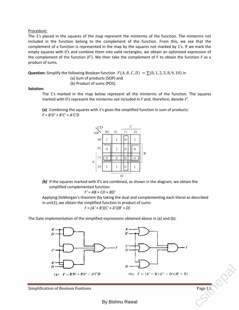
Simplification of Boolean Funtions Page 11
Procedure: The 1's placed in the squares of the map represent the minterms of the function. The minterms not included in the function belong to the complement of the function. From this, we see that the complement of a function is represented in the map by the squares not marked by 1's. If we mark the empty squares with 0's and combine them into valid rectangles, we obtain an optimized expression of the complement of the function (F’). We then take the complement of F to obtain the function F as a product of sums. Question: Simplify the following Boolean function 𝐹(𝐴, 𝐵, 𝐶, 𝐷) = (0, 1, 2, 5, 8, 9, 10) in
(a) Sum of products (SOP) and (b) Product of sums (POS).
Solution: The 1's marked in the map below represent all the minterms of the function. The squares marked with 0's represent the minterms not included in F and, therefore, denote F’. (a) Combining the squares with 1's gives the simplified function in sum of products: F = B'D' + B'C' + A'C'D
(b) If the squares marked with 0's are combined, as shown in the diagram, we obtain the
simplified complemented function: F' = AB + CD + BD'
Applying DeMorgan's theorem (by taking the dual and complementing each literal as described in unit2), we obtain the simplified function in product of sums:
F = (A' + B')(C' + D')(B' + D) The Gate implementation of the simplified expressions obtained above in (a) and (b):
csitn
epal
By Bishnu Rawal

Simplification of Boolean Funtions Page 12
NAND and NOR implementation Digital circuits are more frequently constructed with NAND or NOR gates than with AND and OR gates. NAND and NOR gates are easier to fabricate with electronic components and are the basic gates used in all IC digital logic families. The procedure for two-level implementation is presented in this section.
NAND and NOR conversions (from AND, OR and NOT implemented Boolean functions) Because of the prominence of NAND and NOR gates in the design of digital circuits, rules and procedures have been developed for the conversion from Boolean functions given in terms of AND, OR, and NOT into equivalent NAND and NOR logic diagrams. To facilitate the conversion to NAND and NOR logic, there are two other graphic symbols for these gates.
(a) NAND gate Two equivalent symbols for the NAND gate are shown in diagram below:
Fig: Two graphic symbols for NAND gate
(b) NOR gate
Fig: Two graphic symbols for NOR gate
(c) Inverter
Fig: Three graphic symbols for NOT gate
NAND implementation The implementation of a Boolean function with NAND gates requires that the function be simplified in the sum of products form. To see the relationship between a sum of products expression and its equivalent NAND implementation, consider the logic diagrams of Fig below. All three diagrams are equivalent and implement the function: F=AB + CD + E
csitn
epal
By Bishnu Rawal

Simplification of Boolean Funtions Page 13
The rule for obtaining the NAND logic diagram from a Boolean function is as follows: First method:
(a) Simplify the function and express it in sum of products. (b) Draw a NAND gate for each product term of the function that has at least two literals. The
inputs to each NAND gate are the literals of the term. This constitutes a group of first-level gates.
(c) Draw a single NAND gate (using the AND-invert or invert-OR graphic symbol) in the second level, with inputs coming from outputs of first-level gates.
(d) A term with a single literal requires an inverter in the first level or may be complemented and applied as an input to the second-level NAND gate.
Second method: If we combine the 0's in a map, we obtain the simplified expression of the complement of the function in sum of products. The complement of the function can then be implemented with two levels of NAND gates using the rules stated above. If the normal output is desired, it would be necessary to insert a one-input NAND or inverter gate. There are occasions where the designer may want to generate the complement of the function; so this second method may be preferable. Question: Implement the following function with NAND gates: 𝐹(𝑥, 𝑦, 𝑧) = (0, 6) Solution:
The first step is to simplify the function in sum of products form. This is attempted with the map. There are only two 1's in the map, and they can’t be combined.
Fig: Map simplification in SOP
METHOD1: Two-level NAND implementation is shown below:
Fig: F = x'y'z' +xyz'
METHOD2:
Next we try to simplify the complement of the function in sum of products. This is done by combining the 0's in the map:
csitn
epal
By Bishnu Rawal

Simplification of Boolean Funtions Page 14
F' = x'y + xy' + z The two-level NAND gate for generating F' is shown below:
Fig: F' = x'y + xy' + z
If output F is required, it is necessary to add a one· input NAND gate to invert the function. This gives a three-level implementation.
NOR Implementation The NOR function is the dual of the NAND function. For this reason, all procedures and rules for NOR logic are the duals of the corresponding procedures and rules developed for NAND logic. The implementation of a Boolean function with NOR gates requires that the function be simplified in product of sums form. A product of sums expression specifies a group of OR gates for the sum terms, followed by an AND gate to produce the product. The transformation from the OR-AND to the NOR-NOR diagram is depicted in Fig below. It is similar to the NAND transformation discussed previously, except that now we use the product of sums expression.
Fig: Three ways to implement F = (A + B) (C + D)E All the rules for NOR implementation are similar to NAND except that these are duals, so I won’t describe them here. Question: Implement the following function with NOR gates: 𝐹(𝑥, 𝑦, 𝑧) = (0, 6) Solution:
Map is drawn in previous question.
csitn
epal
By Bishnu Rawal

Simplification of Boolean Funtions Page 15
Summary of NAND and NOR implementation
METHOD1 First, combine the 0's in the map to obtain F'=x'y+xy'+z this is the complement of the function in sum of products. Complement F' to obtain the simplified function in product of sums as required for NOR implementation:
F = (x + y') (x' + y) z'
METHOD2 A second implementation is possible from the complement of the function in product of sums. For this case, first combine the 1's in the map to obtain
F = x'y'z' +xyz' Complement this function to obtain the complement of the function in product of sums as required for NOR implementation:
F' = (x + y + z)(x' + y' + z)
csitn
epal
By Bishnu Rawal

Combinational Logic Page 1
Unit 4 Combinational Logic
Introduction In digital circuit theory, combinational logic is a type of digital logic which is implemented by Boolean circuits, where the output is a pure function of the present input only. This is in contrast to sequential logic, in which the output depends not only on the present input but also on the history of the input. In other words, sequential logic has memory while combinational logic does not.
Combinational Circuit These are the circuit gates employing combinational logic.
A combinational circuit consists of n input variables, logic gates, and m output variables. The logic gates accept signals from the inputs and generate signals to the outputs.
For n input variables, there are 2n possible combinations of binary input values. For each possible input combination, there is one and only one possible output combination. A combinational circuit can be described by m Boolean functions, one for each output variable. Each output function is expressed in terms of the n input variables.
Obviously, both input and output data are represented by binary signals, i.e., logic-1 and the other logic-0. The n input binary variables come from an external source; the m output variables go to an external destination. A block diagram of a combinational circuit is shown in Fig:
Fig: Block diagram of combinational circuit
Design procedure The design of combinational circuits starts from the verbal outline of the problem and ends in a logic circuit diagram or a set of Boolean functions from which the logic diagram can be easily obtained. The procedure involves the following steps:
1. Specification Write a specification for the circuit if one is not already available
2. Formulation Derive a truth table or initial Boolean equations that define the required relationships
between the inputs and outputs, if not in the specification. Apply hierarchical design if appropriate
3. Optimization Apply 2-level and multiple-level optimization Draw a logic diagram for the resulting circuit using ANDs, ORs, and inverters
4. Technology Mapping Map the logic diagram to the implementation technology selected
5. Verification Verify the correctness of the final design manually or using simulation
csitn
epal
By Bishnu Rawal

Combinational Logic Page 2
In simple words, we can list out the design procedure of combinational circuits as: 1. The problem is stated. 2. The number of available input variables and required output variables is determined. 3. The input and output variables are assigned letter symbols. 4. The truth table that defines the required relationships between inputs and outputs is derived. 5. The simplified Boolean function for each output is obtained. 6. The logic diagram is drawn.
Adders Digital computers perform a variety of information-processing tasks. Among the basic functions encountered are the various arithmetic operations. The most basic arithmetic operation, no doubt, is the addition of two binary digits.
Half-Adder
A combinational circuit that performs the addition of two bits is called a half-adder.
Circuit needs two inputs and two outputs. The input variables designate the augend (x) and addend (y) bits; the output variables produce the sum (S) and carry (C).
Now we formulate a Truth table to exactly identify the function of half-adder.
The simplified Boolean functions for the two outputs can be obtained directly from the truth
table. The simplified sum of products expressions are:
S = x'y + xy'
C = xy
Implementation:
csitn
epal
By Bishnu Rawal

Combinational Logic Page 3
Other realizations and implementations of Half-adders are:
Full-Adder
A full-adder is a combinational circuit that forms the arithmetic sum of three input bits.
It consists of three inputs and two outputs. Two of the input variables, denoted by x and y, represent the two significant bits to be added. The third input, z, represents the carry from the previous lower significant position.
Truth table formulation:
The input-output logical relationship of the full-adder circuit may be expressed in two Boolean
functions, one for each output variable. Each output Boolean function requires a unique map for
its simplification (maps are not necessary; you guys can use algebraic method for simplification).
Simplified expression in sum of products can be obtained as:
The S output is equal to 1 when only one
input is equal to 1 or when all three
inputs are equal to 1. The C output has a
carry of 1 if two or three inputs are equal
to 1.
csitn
epal
By Bishnu Rawal

Combinational Logic Page 4
S = x'y'z + x'yz' + xy'z' + xyz C = xy + xz + yz
Implementation:
Fig: Implementation of a full-adder in sum of products.
A full-adder can be implemented with two half-adders and one OR gate.
Fig: Implementation of a full-adder with two half-adders and an OR gate
Here, The S output from the second half-adder is the exclusive-OR of z and the output of the
first half-adder, giving:
S = z ⊕ (x ⊕ y)
= z'(xy' + x'y) + z(xy' + x'y)'
= z'(xy' + x'y) + z(xy + x'y')
= xy'z' + x'yz' + xyz + x'y'z
Subtractors The subtraction of two binary numbers may be accomplished by taking the complement of the subtrahend and adding it to the minuend. By this method, the subtraction operation becomes an
C = z (x ⊕ y) + xy
= z(xy' + x'y) + xy
= xy'z + x'yz + xy
csitn
epal
By Bishnu Rawal

Combinational Logic Page 5
addition operation requiring full-adders for its machine implementation. It is possible to implement subtraction with logic circuits in a direct manner, as done with paper and pencil. By this method, each subtrahend bit of the number is subtracted from its corresponding significant minuend bit to form a difference bit. If the minuend bit is smaller than the subtrahend bit, a 1 is borrowed from the next significant position. Just as there are half- and full-adders, there are half- and full-subtractors.
Half-Subtractor
A half-subtractor is a combinational circuit that subtracts two bits and produces their difference bit.
Denoting minuend bit by x and the subtrahend bit by y. To perform x - y, we have to check the relative magnitudes of x and y:
o If x≥ y, we have three possibilities: 0 - 0 = 0, 1 - 0 = 1, and 1 - 1 = 0. o If x < y, we have 0 - 1, and it is necessary to borrow a 1 from the next higher stage.
The half-subtractor needs two outputs, difference (D) and borrow (B).
The truth table for the input-output relationships of a half-subtractor can now be derived as follows:
The Boolean functions for the two outputs of the half-subtractor are derived directly from the truth table:
D = x'y + xy' B = x'y
Implementation for Half-subtractor is similar to Half-adder except the fact that x input of B is inverted. (Here, D is analogous to S and B is similar to C of half-adder circuit). Try it out, I don’t like redundancy…
Full-Subtractor A full-subtractor is a combinational circuit that performs a subtraction between two bits, taking
into account that a 1 may have been borrowed by a lower significant stage.
This circuit has three inputs and two outputs. The three inputs, x, y, and z, denote the minuend, subtrahend, and previous borrow, respectively. The two outputs, D and B, represent the difference and output-borrow, respectively.
Truth-table and output-function formulation:
The output borrow B is a 0 as long as x≥ y. It is a 1 for x = 0 and y = 1. The D output is the result of the arithmetic operation 2B + x - y.
csitn
epal
By Bishnu Rawal

Combinational Logic Page 6
The simplified Boolean functions for the two outputs of the full-subtractor are derived in the maps:
D = x'y'z + x'yz' + xy'z' + xyz B = x'y + x'z + yz
Circuit implementations are same as Full-adder except B output (analogous to C) is little
different. (Don’t worry! ladies and gentlemen, we will discuss it in class…)
Code Conversion
The availability of a large variety of codes for the same discrete elements of information results in the use of different codes by different digital systems. It is sometimes necessary to use the output of one system as the input to another. A conversion circuit must be inserted between the two systems if each uses different codes for the same information. Thus, a code converter is a circuit that makes the two systems compatible even though each uses a different binary code.
To convert from binary code A to binary code B, code converter has input lines supplying the bit combination of elements as specified by code A and the output lines of the converter generating the corresponding bit combination of code B. A Code converter (combinational circuit) performs this transformation by means of logic gates.
The design procedure of code converters will be illustrated by means of a specific example of conversion from the BCD to the excess-3 code. I will describe 5-step design procedure of this code converter so that you guys will be able to understand how practical combinational circuits are designed.
The 1's and 0's for the output variables are determined from the subtraction of x - y - z.
The combinations having input borrow z = 0 reduce to the same four conditions of the half-adder.
For x = 0, y = 0, and z = 1, we have to borrow a 1 from the next stage, which makes B = 1 and adds 2 to x. Since 2 - 0 - 1 = 1, D = 1.
For x = 0 and yz = 11, we need to borrow again, making B = 1 and x = 2. Since 2 - 1 - 1 = 0, D = 0.
For x = 1 and yz = 01, we have x - y - z = 0, which makes B = 0 and D = 0.
Finally, for x = 1, y = 1, z =1I, we have to borrow 1, making B = 1 and x = 3, and 3 - 1 - 1 = 1, making D=1.
csitn
epal
By Bishnu Rawal

Combinational Logic Page 7
Design example: BCD to Excess-3 code converter
1. Specification Transforms BCD code for the decimal digits to Excess-3 code for the decimal digits BCD code words for digits 0 through 9: 4-bit patterns 0000 to 1001, respectively. Excess-3 code words for digits 0 through 9: 4-bit patterns consisting of 3 (binary 0011)
added to each BCD code word Implementation:
o multiple-level circuit 2. Formulation
Conversion of 4-bit codes can be most easily formulated by a truth table Variables- BCD: A, B, C, D
Variables- Excess-3: W, X, Y, Z
Don’t Cares: BCD 1010 to 1111
Table: Truth table for code converter example 3. Optimization
a. 2-level optimization The k-maps are plotted to obtain simplified sum-of-products Boolean expressions for the outputs. Each of the four maps represents one of the outputs of the circuit as a function of the four inputs.
Note that the four BCD input variables may have 16 bit combinations, but only 10 are listed in the truth table. Others designate “don’t care conditions”.
csitn
epal
By Bishnu Rawal

Combinational Logic Page 8
b. Multiple-level optimization
This second optimization step reduces the number of gate inputs (and hence the no. gates). The following manipulation illustrates optimization with multiple-output circuits implemented with three levels of gates:
Fig: Logic Diagram of BCD- to-Excess-3 Code Converter
4. Technology mapping
This is concerned with the act of mapping of basic circuit (using AND, OR and NOT gates) to a specific circuit technology (such as NAND, NOR gate tech.).
csitn
epal
By Bishnu Rawal

Combinational Logic Page 9
HEY! This is advanced topic, and I won’t discuss here. For exam point of view, if you are asked for BCD-to-Excess-3 code converter, you will finish up your answer by drawing basic circuit shown above.
5. Verification Here we need to test our designed circuit, whether it works correctly. You guys are so keen; hope you can do it….
Analysis Procedure The design of a combinational circuit starts from the verbal specifications of a required function and ends with a set of output Boolean functions or a logic diagram. The analysis of a combinational circuit is somewhat the reverse process. It starts with a given logic diagram and culminates with a set of Boolean functions, a truth table, or a verbal explanation of the circuit operation.
Obtaining Boolean functions from logic diagram Steps in analysis:
1. The first step in the analysis is to make sure that the given circuit is combinational and not sequential.
2. Assign symbols to all gate outputs that are a function of the input variables. Obtain the Boolean functions for each gate.
3. Label with other arbitrary symbols those gates that are a function of input variables and/or previously labeled gates. Find the Boolean functions for these gates.
4. Repeat step 3 until the outputs of the circuit are obtained. 5. By repeated substitution of previously defined functions, obtain the output Boolean functions in
terms of input variables only. Analysis of the combinational circuit below illustrates the proposed procedure:
csitn
epal
By Bishnu Rawal

Combinational Logic Page 10
We note that the circuit has three binary inputs, A, B, and C, and two binary outputs, F1 and F2. The outputs of various gates are labeled with intermediate symbols. The outputs of gates that are a function of input variables only are F2, T1 and T2. The Boolean functions for these three outputs are
F2 = AB + AC + BC T1=A+B+C T2 = ABC
Next we consider outputs of gates that are a function of already defined symbols: T3 = F2’T1 F1 = T3 + T2
The output Boolean function F2 just expressed is already given as a function of the in puts only. To obtain F1 as a function of A, B, and C, form a series of substitutions as follows:
If you want to determine the information-transformation task achieved by this circuit, you can derive the truth table directly from the Boolean functions and try to recognize a familiar operation. For this example, we note that the circuit is a full-adder, with F, being the sum output and F, the carry output. A, B, and C are the three inputs added arithmetically. Obtaining truth-table from logic diagram The derivation of the truth table for the circuit is a straightforward process once the output Boolean functions are known. To obtain the truth table directly from the logic diagram without going through the derivations of the Boolean functions, proceed as follows: Steps in analysis:
1. Determine the number of input variables to the circuit. For n inputs, form the 2n possible input combinations of 1's and 0's by listing the binary numbers from 0 to 2n – 1.
2. Label the outputs of selected gates with arbitrary symbols. 3. Obtain the truth table for the outputs of those gates that are a function of the input variables
only. 4. Proceed to obtain the truth table for the outputs of those gates that are a function of
previously defined values until the columns for all outputs are determined.
This process can be illustrated using the circuit above: We form the eight possible combinations for the three input variables. The truth table for F2 is determined directly from the values of A, B, and C, with F2 equal to 1 for any combination that has two or three inputs equal to 1. The truth table for F2’ is the complement of F2. The truth tables for T1 and T2 are the OR and AND functions of the input variables, respectively. The values for T3 are derived from T1 and F2’. T3 is equal to 1 when both T1 and F2’ are equal to 1, and to 0 otherwise. Finally, F1 is equal to 1 for those combinations in which either T2 or T3 or both are equal to 1.
csitn
epal
By Bishnu Rawal

Combinational Logic Page 11
Inspection of the truth-table combinations for A, B, C, F1 and F2 of table above shows that it is identical to the truth-table of the full-adder.
HEY! When a circuit with don't-care combinations is being analyzed, the situation is entirely different. We assume here that the don't-care input combinations will never occur.
NAND, NOR and Ex-OR circuits
In unit 3, SOP and POS form of Boolean functions are studied. Also we got to know, Such Boolean functions can be implemented with 2-level circuits using universal gates (look at NAND and NOR implementation of Boolean function, unit 3). Here we will look at the multiple level circuits employing universal gates i.e we will treat the functions which are in standard form.
Multi-level NAND circuits To implement a Boolean function with NAND gates we need to obtain the simplified Boolean function in terms of Boolean operators and then convert the function to NAND logic. The conversion of an algebraic expression from AND, OR, and complement to NAND can be done by simple circuit-manipulation techniques that change AND-OR diagrams to NAND diagrams. To obtain a multilevel NAND diagram from a Boolean expression, proceed as follows:
1. From the given Boolean expression, draw the logic diagram with AND, OR, and inverter gates. Assume that both the normal and complement inputs are available.
2. Convert all AND gates to NAND gates with AND-invert graphic symbols. 3. Convert all OR gates to NAND gates with invert-OR graphic symbols. 4. Check all small circles in the diagram. For every small circle that is not compensated by another
small circle along the same line, insert an inverter (one-input NAND gate) or complement the input variable.
Example: F = A + (B' + C) (D' + BE ')
AND-OR diagram NAND diagram using two graphic symbols
csitn
epal
By Bishnu Rawal

Combinational Logic Page 12
NAND diagram using one graphic symbol
Multi-level NOR circuits The NOR function is the dual of the NAND function. For this reason, all procedures and rules for NOR logic form a dual of the corresponding procedures and rules developed for NAND logic. Similar to NAND, NOR has also two graphic symbols: OR-invert and invert-AND symbol. The procedure for implementing a Boolean function with NOR gates is similar to the procedure outlined in the previous section for NAND gates:
1. Draw the AND-OR logic diagram from the given algebraic expression. Assume that both the normal and complement inputs are available.
2. Convert all OR gates to NOR gates with OR-invert graphic symbols. 3. Convert all AND gates to NOR gates with invert-AND graphic symbols. 4. Any small circle that is not compensated by another small circle along the same line needs
an inverter or the complementation of the input variable. Example: F = (AB + E) (C + D)
AND-OR diagram NOR diagram
Alternate NOR diagram
csitn
epal
By Bishnu Rawal

Combinational Logic Page 13
Ex-OR function
The exclusive-OR (XOR) denoted by the symbol ⊕, is a logical operation that performs the following Boolean operation:
x ⊕ y = xy' + x'y It is equal to 1 if only x is equal to 1 or if only y is equal to 1 but not when both are equal. Realization of XOR using Basic gates and universal gates A two-input exclusive-OR function is constructed with conventional gates using two inverters, two AND gates, and an OR gate and next firgure shows the implementation of the exclusive-OR with four NAND gates.
Fig: Implementation XOR with AND-OR-NOT gates
Fig: Realization of XOR with NAND gates
In second diagram, first NAND gate performs the operation (xy)' = (x' + y'). The other two-level NAND circuit produces the sum of products of its inputs:
(x' + y')x + (x' + y')y = xy' + x'y = x ⊕ y Only a limited number of Boolean functions can be expressed in terms of exclusive-OR operations. Nevertheless, this function emerges quite often during the design of digital systems. It is particularly useful in arithmetic operations and error-detection and correction circuits.
Parity generator and Checker Exclusive-OR functions are very useful in systems requiring error-detection and correction codes. As discussed before, a parity bit is used for the purpose of detecting errors during transmission of binary information. A parity bit is an extra bit included with a binary message to make the number of 1's either odd or even. The message, including the parity bit, is transmitted and then checked at the receiving end for errors. An error is detected if the checked parity does not correspond with the one transmitted.
The circuit that generates the parity bit in the transmitter is called a parity generator.
csitn
epal
By Bishnu Rawal

Combinational Logic Page 14
The circuit that checks the parity in the receiver is called a parity checker. Example: Consider a 3-bit message to be transmitted together with an even parity bit. The three bits, x, y, and z, constitute the message and are the inputs to the circuit. The parity bit P is the output. For even parity, the bit P must be generated to make the total number of 1’s even (including P).
Table: Even parity generator truth table The three bits in the message together with the parity bit are transmitted to their destination, where they are applied to a parity-checker circuit to check for possible errors in the transmission.
Table: Even parity checker truth table
From the truth table, we see that P constitutes an odd function because it is equal to 1 for those minterms whose numerical values have an odd number of 1’s. Therefore, P can be expressed as a three-variable exclusive-OR function: P = x ⊕ y ⊕ z.
Since the information was transmitted with
even parity, the four bits received must have
an even number of 1's. An error occurs during
the transmission if the four bits received have
an odd number of 1's, indicating that one bit
has changed in value during transmission.
The output of the parity checker, denoted by
C, will be equal to 1 if an error occurs, that is,
if the four bits received have an odd number
of 1’s.
The parity checker can be implemented with
exclusive-OR gates: C = x ⊕y ⊕z ⊕ P.
csitn
epal
By Bishnu Rawal

Combinational Logic Page 15
Logic diagrams for parity generator and Parity checker are shown below:
csitn
epal
By Bishnu Rawal

Combinational Logic with MSI and LSI Page 1
Unit 5 Combinational Logic with MSI and LSI
(I have included Point! ‘s throughout the chapter to designate extra things you need to know about the concerned topic and are unimportant for the exam point of view.)
Introduction The purpose of Boolean-algebra simplification is to obtain an algebraic expression that, when implemented, results in a low-cost circuit. Two circuits that perform the same function, the one that requires fewer gates is preferable because it will cost less. But this is not necessarily true when integrated circuits are used. With integrated circuits, it is not the count of gates that determines the cost, but the number and types of ICs employed and the number of interconnections needed to implement the digital circuits of varying complexities (I mean circuits with different level of integrations viz. SSI, MSI, LSI, VLSI, ULSI etc). There are several combinational circuits that are employed extensively in the design of digital systems. These circuits are available in integrated circuits and are classified as MSI components. MSI components perform specific digital functions commonly needed in the design of digital systems.
Combinational circuit-type MSI components that are readily available in IC packages are binary adders, subtractors, comparators, decoders, encoders, and multiplexers. These components are also used as standard modules within more complex LSI and VLSI circuits and hence used extensively as basic building blocks in the design of digital computers and systems.
Binary Adder This circuit sums up two binary numbers A and B of n-bits using full-adders to add each bit-pair & carry from previous bit position. The sum of A and B can be generated in two ways: either in a serial fashion or in parallel.
The serial addition method uses only one full-adder circuit and a storage device to hold the generated output carry. The pair of bits in A and B are transferred serially, one at a time, through the single full-adder to produce a string of output bits for the sum. The stored output carry from one pair of bits is used as an input carry for the next pair of bits.
The parallel method uses n full-adder circuits, and all bits of A and B are applied simultaneously. The outputs carry from one full-adder is connected to the input carry of the full-adder one position to its left. As soon as the carries are generated, the correct sum bits emerge from the sum outputs of all full-adders.
Binary Parallel adder A binary parallel adder is a digital circuit that produces the arithmetic sum of two binary numbers in parallel. It consists of full-adders connected in a chain, with the output carry from each full-adder connected to the input carry of the next full-adder in the chain. Diagram below shows the interconnection of four full-adder (FA) circuits to provide a 4-bit binary parallel adder. The augend bits of A and the addend bits of B are designated by subscript numbers from right to left. The carries are connected in a chain through the full-adders. The S outputs generate the required sum bits. The input carry to the adder is C1 and the output carry is C5.
csitn
epal
By Bishnu Rawal

Combinational Logic with MSI and LSI Page 2
When the 4-bit full-adder circuit is enclosed within an IC package, it has four terminals for the augend bits, four terminals for the addend bits, four terminals for the sum bits, and two terminals for the input and output carries.
Fig: 4-bit parallel binary adder Point-1! (To be noted my Boys…) The 4-bit binary-adder is a typical example of an MSI function. It can be used in many applications involving arithmetic operations. Observe that the design of this circuit by the classical method would require a truth table with 29 = 512 entries, since there are 9 inputs to the circuit. By using an iterative method of cascading an already known function, we were able to obtain a simple and well-organized implementation. Point-2!
The carry propagation time is a limiting factor on the speed with which two numbers are added in parallel. Although a parallel adder, or any combinational circuit, will always have some value at its output terminals, the outputs will not be correct unless the signals are given enough time to propagate through the gates connected from the inputs to the outputs. Since all other arithmetic operations are implemented by successive additions, the time consumed during the addition process is very critical. An obvious solution for reducing the carry propagation delay time is to employ faster gates with reduced delays. But physical circuits have a limit to their capability. Another solution is to increase the equipment complexity in such a way that the carry delay time is reduced. There are several techniques for reducing the carry propagation time in a parallel adder. The most widely used technique employs the principle of look-ahead carry.
Decimal Adder
Computers or calculators that perform arithmetic operations directly in the decimal number system represent decimal numbers in binary-coded form.
Decimal adder is a combinational circuit that sums up two decimal numbers adopting particular encoding technique.
A decimal adder requires a minimum of nine inputs and five outputs, since four bits are required to code each decimal digit and the circuit must have an input carry and output carry.
Of course, there is a wide variety of possible decimal adder circuits, dependent upon the code used to represent the decimal digits.
csitn
epal
By Bishnu Rawal

Combinational Logic with MSI and LSI Page 3
BCD Adder This combinational circuit adds up two decimal numbers when they are encoded with binary-coded decimal (BCD) form. Adding two decimal digits in BCD, together with a possible carry, the output sum cannot be greater
than 9 + 9 + 1 = 19. Applying two BCD digits to a 4-bit binary adder, the adder will form the sum in binary ranging from 0
to 19. These binary numbers are listed in Table below and are labeled by symbols K, Z8, Z4, Z2, Z1. K is the carry, and the subscripts under the letter z represent the weights 8, 4, 2, and 1 that can be assigned to the four bits in the BCD code.
Looking at the table, we see that: When (binary sum) <= 1001
Corresponding BCD number is identical, and therefore no conversion is needed. When (binary sum) > 1001
Non-valid BCD representation is obtained. The addition of binary 6 (0110) to the binary sum converts it to the correct BCD representation and also produces an output carry as required.
The logic circuit that detects the necessary correction can be derived from the table entries. Correction is needed when
o The binary sum has an output carry K = 1. o The other six combinations from 1010 to 1111 that have Z8=1. To distinguish them from
binary 1000 and 1001, which also have a 1 in position Z8, we specify further that either Z4 or Z2 must have a 1. The condition for a correction and an output carry can be expressed by the Boolean function
C = K + Z8Z4 + Z8Z2 When C = 1, it is necessary to add 0110 to the binary sum and provide an output carry for the next
stage.
The first column in the table lists the binary sums as they appear in the outputs of a 4-bit binary adder.
The output sum of two decimal digits must be represented in BCD and should appear in the form listed in the second column.
The problem is to find a simple rule by which the binary number, in the first column can be converted to the correct BCD-digit representation of the number in the second column.
csitn
epal
By Bishnu Rawal

Combinational Logic with MSI and LSI Page 4
Fig: Block diagram of BCD adder
A decimal parallel adder that adds n decimal digits needs n BCD adder stages. The output carry from one
stage must be connected to the input carry of the next higher order stage.
Point! The BCD adder can be constructed with three IC packages. Each of the 4-bit adders is an MST function and the three gates for the correction logic need one SST package. However, the BCD adder is available in one MSI circuit. To achieve shorter propagation delays, an MSI BCD adder includes the necessary circuits for look-ahead carries. The adder circuit for the correction does not need all four full-adders, and this circuit can be optimized within the IC package.
Magnitude Comparator A Magnitude comparator is a combinational circuit that compares two numbers, A and B, and determines their relative magnitudes. The outcome of the comparison is specified by three binary variables that indicate whether A > B, A = B, or A < B. Consider two numbers, A and B, with four digits each. Write the coefficients of the numbers with descending significance as follows:
A = A3A2A1A0 B = B3B2B1B0
Where each subscripted letter represents one of the digits in the number, the two numbers are equal if all pairs of significant digits are equal, i.e., if A3 = B3 and A2 = B2 and A1 = B1 and A0 = B0. When the numbers are binary, the digits are either 1 or 0 and the equality relation of each pair of bits can be expressed logically with an equivalence function:
Xi = AiBi + Ai’Bi’, i = 0, 1, 2, 3 Where Xi = 1 only if the pair of bits in position i are equal, i.e., if both are 1's or both are 0's.
A BCD adder is a circuit that adds two BCD digits in parallel and produces a sum digit also in BCD.
BCD adder must include the correction logic in its internal construction.
To add 0110 to the binary sum, we use a second 4-bit binary adder, as shown in diagram.
The two decimal digits, together with the input carry, are first added in the top 4-bit binary adder to produce the binary sum.
When the output carry = 0, nothing is added to the binary sum. When it is equal to 1, binary 0110 is added to the binary sum through the bottom 4-bit binary adder.
The output carry generated from the bottom binary adder can be ignored, since it supplies information already available at the output-carry terminal.
csitn
epal
By Bishnu Rawal
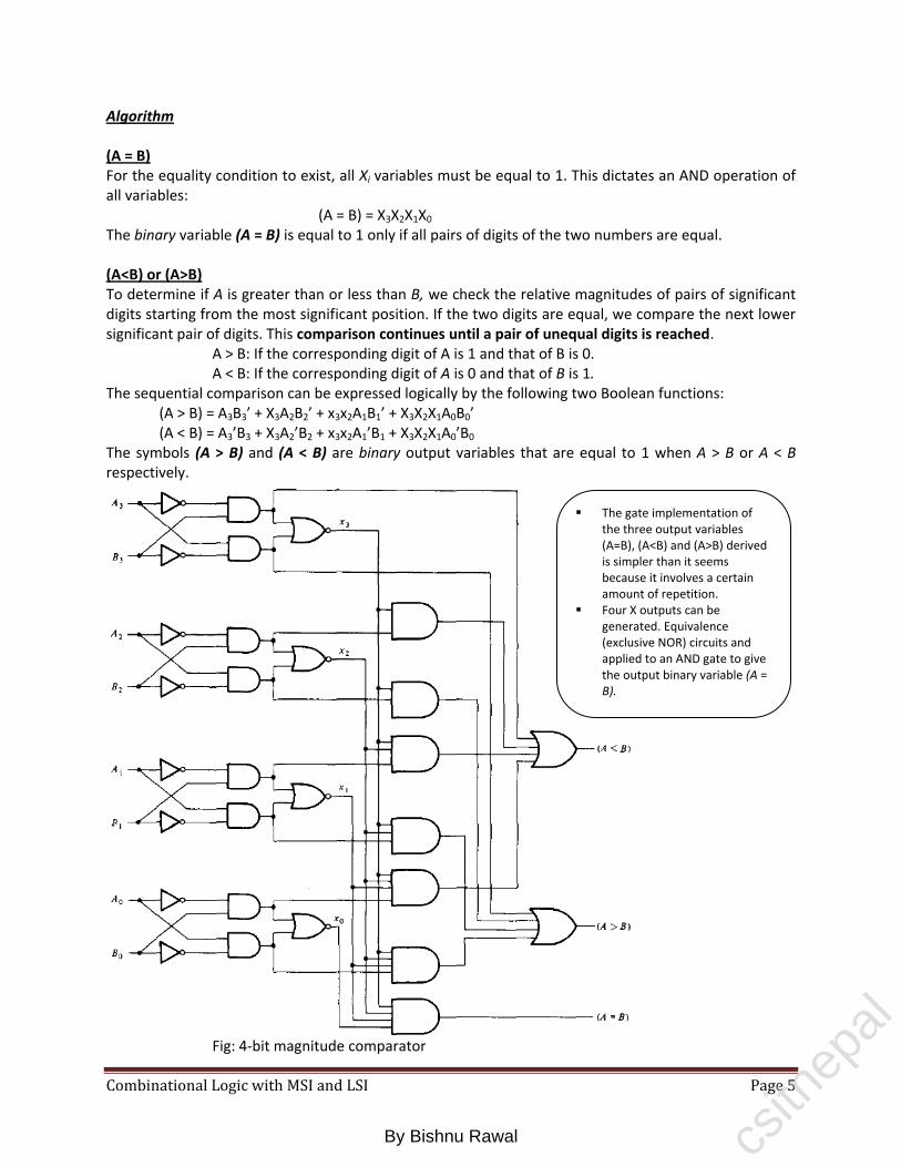
Combinational Logic with MSI and LSI Page 5
Algorithm (A = B) For the equality condition to exist, all Xi variables must be equal to 1. This dictates an AND operation of all variables:
(A = B) = X3X2X1X0 The binary variable (A = B) is equal to 1 only if all pairs of digits of the two numbers are equal. (A<B) or (A>B) To determine if A is greater than or less than B, we check the relative magnitudes of pairs of significant digits starting from the most significant position. If the two digits are equal, we compare the next lower significant pair of digits. This comparison continues until a pair of unequal digits is reached.
A > B: If the corresponding digit of A is 1 and that of B is 0. A < B: If the corresponding digit of A is 0 and that of B is 1.
The sequential comparison can be expressed logically by the following two Boolean functions: (A > B) = A3B3’ + X3A2B2’ + x3x2A1B1’ + X3X2X1A0B0’ (A < B) = A3’B3 + X3A2’B2 + x3x2A1’B1 + X3X2X1A0’B0
The symbols (A > B) and (A < B) are binary output variables that are equal to 1 when A > B or A < B respectively.
Fig: 4-bit magnitude comparator
The gate implementation of the three output variables (A=B), (A<B) and (A>B) derived is simpler than it seems because it involves a certain amount of repetition.
Four X outputs can be generated. Equivalence (exclusive NOR) circuits and applied to an AND gate to give the output binary variable (A = B).
csitn
epal
By Bishnu Rawal

Combinational Logic with MSI and LSI Page 6
Decoders and Encoders
Discrete quantities of information are represented in digital systems with binary codes. A binary code of n bits is capable of representing up to 2n distinct elements of the coded information. Decoder is a combinational circuit that converts binary information from n input lines to a maximum
of 2n unique output lines. o If the n-bit decoded information has unused or don't-care combinations, the decoder output
will have fewer than 2n outputs. o n-to-m-line decoders have m <= 2n.
Encoder is a digital circuit that performs the inverse operation of a decoder. An encoder has 2n (or fewer) input lines and n output lines. The output lines generate the binary code corresponding to the input value.
o An example of an encoder is the octal-to-binary encoder which has eight inputs, one for each of the octal digits, and three outputs that generate the corresponding binary number.
Example: 3-to-8 line decoder The 3 inputs are decoded into 8 outputs, each output representing one of the minterms of the 3-input variables.
Fig: 3-to-8 line decoder
Table: Truth-table for 3-to-8 line Decoder
Output variables are mutually exclusive because only one output can be equal to 1 at anyone time. The output line whose value is equal to 1 represents the minterm equivalent of the binary number presently available in the input lines.
csitn
epal
By Bishnu Rawal

Combinational Logic with MSI and LSI Page 7
Combinational logic Implementation A decoder provides the 2n minterm of n input variables. Since any Boolean function can be expressed in sum of minterms canonical form, one can use a decoder to generate the minterms and an external OR gate to form the sum.
Any combinational circuit with n inputs and m outputs can be implemented with an n-to-2n-line decoder and m OR gates.
Boolean functions for the Decoder-implemented-circuit are expressed in sum of minterms. This form can be easily obtained from the truth table or by expanding the functions to their sum of minterms.
Example: Implement a full-adder circuit with a decoder. Solution: From the truth table of the full-adder, we obtain the functions for this combinational circuit in sum of minterms as:
Since there are three inputs and a total of eight minterms, we need a 3-to-8-line decoder.
Fig: Implementation of Full-adder with a decoder circuit
Multiplexers
A digital multiplexer is a combinational circuit that selects binary information from one of many input lines and directs it to a single output line.
o The selection of a particular input line is controlled by a set of selection lines. o Normally, there are 2n input lines and n selection lines whose bit combinations
determine which input is selected. A demultiplexer is a circuit that receives information on a single line and transmits this
information on one of 2n possible output lines. The selection of a specific output line is controlled by the bit values of n selection lines.
o A Decoder with an enable input can function as a demultiplexer. o Here, enable input and input variables for decoder is taken as data input line and
selection lines for the demultiplexer respectively.
Decoder generates the eight minterms for x, y, z. The OR gate for output S
forms the sum of minterms 1, 2, 4, and 7.
The OR gate for output C forms the sum of minterms 3, 5, 6, and 7.
csitn
epal
By Bishnu Rawal

Combinational Logic with MSI and LSI Page 8
Fig: Logic Diagram: 4-to-1 line Multiplexer Boolean Function implementation As decoder can be used to implement a Boolean function by employing an external OR gate, we can implement any Boolean function (in SOP) with multiplexer since multiplexer is essentially a decoder with the OR gate already available.
If we have a Boolean function of n + 1 variables, we take n of these variables and connect them to the selection lines of a multiplexer. The remaining single variable of the function is used for the inputs of the multiplexer. If A is this single variable, the inputs of the multiplexer are chosen to be either A or A' or 1 or 0. By judicious use of these four values for the inputs and by connecting the other variables to the selection lines, one can implement any Boolean function with a multiplexer.
So, it is possible to generate any function of n + 1 variables with a 2n-to-1 multiplexer.
Example: Implement Boolean function with multiplexer. Solution: The function can be implemented with a 4-to-1 multiplexer, as shown in Fig. below. Two of the variables, B and C, are applied to the selection lines in that order, i.e., B is connected to s1 and C to s0. The inputs of the multiplexer are 0, 1, A and A'.
Table: Function table
Fig: Block Diagram of Multiplexer
DEMO: consider the case when s1s2 = 10. The AND gate associated with input J, has two of its inputs equal to I and the third input connected to I2. The other three AND gates have at least one input equal to 0, which makes their outputs equal to 0. The OR gate output is now equal to the value of I2, thus providing a path from the selected input to the output. A multiplexer is also called a data selector, since it selects one of many inputs and steers the binary information to the output line.
csitn
epal
By Bishnu Rawal

Combinational Logic with MSI and LSI Page 9
Most important thing during this implementation is the implementation table which is derived from following rules: List the inputs of the multiplexer and under them list all the minterms in two rows. The first row lists all those minterms where A is complemented, and the second row all the minterms with A uncomplemented, as shown in above example. Circle all the minterms of the function and inspect each column separately. If the two minterms in a column are not circled, apply 0 to the corresponding multiplexer
input. If the two minterms are circled, apply 1 to the corresponding multiplexer input. If the bottom minterm is circled and the top is not circled, apply A to the corresponding
multiplexer input. If the top minterm is circled and the bottom is not circled, apply A' to the corresponding
multiplexer input. For clearer concept, do the following exercise: Question: Implement the following function with a multiplexer:
Solution: See text book, page no. 189.
Read Only Memory (ROM) A read-only memory (ROM) is a device that includes both the decoder and the OR gates within a single IC package. The connections between the outputs of the decoder and the inputs of the OR gates can be specified for each particular configuration. The ROM is used to implement complex combinational circuits within one IC package or as permanent storage for binary information. A ROM is essentially a memory (or storage) device in which permanent binary information is stored. The binary information must be specified by the designer and is then embedded in the unit to form the required interconnection pattern. ROMs come with special internal electronic fuses that can be "programmed" for a specific configuration. Once the pattern is established, it stays within the unit even when power is turned off and on again.
csitn
epal
By Bishnu Rawal

Combinational Logic with MSI and LSI Page 10
Example: 32 x 4 ROM (unit consists of 32 words of 8 bits each)
Fig: logic construction of a 32 x 4 ROM
Combinational Logic Implementation From the logic diagram of the ROM, it is clear that each output provides the sum of all the minterms of the n input variables. Remember that any Boolean function can be expressed in sum of minterms form. By breaking the links of those minterms not included in the function, each ROM output can be made to represent the Boolean function.
For an n-input, m-output combinational circuit, we need a 2n x m ROM. The blowing of the fuses is referred to as programming the ROM. The designer need only specify a ROM program table that gives the information for the
required paths in the ROM. The actual programming is a hardware procedure that follows the specifications listed in the program table.
Example: Consider a following truth table:
Truth table specifies a combinational circuit with 2 inputs and 2 outputs. The Boolean function can be represented in SOP:
It consists of n input lines and m output lines. Each bit combination of the input variables is called an address. Each bit combination that comes out of the output lines is called a word. The number of bits per word is equal to the number of output lines, m. An address is essentially a binary number that denotes one of the minterms of n variables. The number of distinct addresses possible with n input variables is 2n.
The five input variables are decoded into 32 lines. Each output of the decoder represents one of the minterms of a function of five variables. Each one of the 32 addresses selects one and only one output from the decoder. The address is a 5-bit number applied to the inputs, and the selected minterm out of the decoder is the one marked with the equivalent decimal number. The 32 outputs of the decoder are connected through fuses to each OR gate. Only four of these fuses are shown in the diagram, but actually each OR gate has 32 inputs and each input goes through a fuse that can be blown as desired.
csitn
epal
By Bishnu Rawal

Combinational Logic with MSI and LSI Page 11
Fig: Combinational-circuit implementation with a 4 x 2 ROM This example demonstrates the general procedure for implementing any combinational circuit with a ROM. From the number of inputs and outputs in the combinational circuit, we first determine the size of ROM required. Then we must obtain the programming truth table of the ROM; no other manipulation or simplification is required. The 0's (or 1's) in the output functions of the truth table directly specify those fuses that must be blown to provide the required combinational circuit in sum of min terms form. Question: Design a combinational circuit using a ROM. The circuit accepts a 3-bit number and generates an output binary number equal to the square of the input number. Solution: See text book page no. 184, if any confusion, do ask me (even call me…)
Types of ROM ROMs: For simple ROMs, mask programming is done by the manufacturer during the fabrication process of the unit. The procedure for fabricating a ROM requires that the customer fill out the truth table the ROM is to satisfy. The truth table may be submitted on a special form provided by the manufacturer. The manufacturer makes the corresponding mask for the paths to produce the 1's and 0's according to the customer's truth table. This procedure is costly because the vendor charges the customer a special fee for custom masking a ROM. For this reason, mask programming is economical only if large quantities of the same ROM configuration are to be manufactured. PROMs: Programmable read-only memory or PROM units contain all 0's (or all 1's) in every bit of the stored words. The approach called field programming is applied for fuses in the PROM which are blown by application of current pulses through the output terminals. This allows the user to program the unit in the laboratory to achieve the desired relationship between input addresses and stored words. Special units called PROM programmers are available commercially to facilitate this procedure. In any case, all procedures for programming ROMs are hardware procedures even though the word programming is used. EPROMs: The hardware procedure for programming ROMs or PROMs is irreversible and, once programmed, the fixed pattern is permanent and cannot be altered. Once a bit pattern has been
Diagram shows the internal construction of a 4X2 ROM. It is now necessary to determine which of the eight available fuses must be blown and which should be left intact. This can be easily done from the output functions listed in the truth table. Those minterms that specify an output of 0 should not have a path to the output through the OR gate. Thus, for this particular case, ti1e truth table shows three 0's, and their corresponding fuses to the OR gates must be blown.
csitn
epal
By Bishnu Rawal

Combinational Logic with MSI and LSI Page 12
established, the unit must be discarded if the bit pattern is to be changed. A third type of unit available is called erasable PROM, or EPROM. EPROMs can be restructured to the initial value (all 0's or all 1's) even though they have been changed previously. When an EPROM is placed under a special ultraviolet light for a given period of time, the shortwave radiation discharges the internal gates that serve as contacts. After erasure, the ROM returns to its initial state and can be reprogrammed. EEPROMs: Certain ROMs can be erased with electrical signals instead of ultraviolet light, and these are called electrically erasable PROMs, or EEPROMs.
Point! The function of a ROM can be interpreted in two different ways:
The first interpretation is of a unit that implements any combinational circuit. From this point of view, each output terminal is considered separately as the output of a Boolean function expressed in sum of minterms.
The second interpretation considers the ROM to be a storage unit having a fixed pattern of bit strings called words. From this point of view, the inputs specify an address to a specific stored word, which is then applied to the outputs. This is the reason why the unit is given the name read-only memory. Memory is commonly used to designate a storage unit. Read is commonly used to signify that the contents of a word specified by an address in a storage unit is placed at the output terminals. Thus, a ROM is a memory unit with a fixed word pattern that can be read out upon application of a given address.
Programmable Logic Array (PLA) A combinational circuit may occasionally have don't-care conditions. When implemented with a ROM, a don't care condition becomes an address input that will never occur. The words at the don't-care addresses need not be programmed and may be left in their original state (all 0's or all 1's). The result is that not all the bit patterns available in the ROM are used, which may be considered a waste of available equipment. Defn: Programmable Logic Array or PLA is LSI component that can be used in economically as an alternative to ROM where number of don’t-care conditions is excessive. Difference between ROM and PLA
ROM PLA
1. ROM generates all the minterms as an output of decoder.
1. PLA does not provide full decoding of the variables.
2. Uses decoder 2. Decoder is replaced by group of AND gates
each of which can be programmed to generate a product term of the input variables.
3. The size of the PLA is specified by the number of inputs (n) and the number of outputs (m).
3. The size of the PLA is specified by the number of inputs (n), the number of product terms (k), and the number of outputs (m) (=number of sum terms)
4. No. of programmed fuses = 2n * m 4. No. of programmed fuses = 2n * k + k * m + m
csitn
epal
By Bishnu Rawal

Combinational Logic with MSI and LSI Page 13
Block Diagram of PLA A block diagram of the PLA is shown in Fig. below. It consists of n inputs, m outputs, k product terms, and m sum terms. The product terms constitute a group of k AND gates and the sum terms constitute a group of m OR gates. Fuses are inserted between all n inputs and their complement values to each of the AND gates. Fuses are also provided between the outputs of the AND gates and the inputs of the OR gates.
Fig: PLA block diagram
PLA program table and Boolean function Implementation The use of a PLA must be considered for combinational circuits that have a large number of inputs and outputs. It is superior to a ROM for circuits that have a large number of don't-care conditions. Let me explain the example to demonstrate how PLA is programmed. Consider a truth table of the combinational circuit:
PLA implements the functions in their sum of products form (standard form, not necessarily canonical as with ROM). Each product term in the expression requires an AND gate. It is necessary to simplify the function to a minimum number of product terms in order to minimize the number of AND gates used. The simplified functions in sum of products are obtained from the following maps:
There are three distinct product terms in this combinational circuit: AB’, AC and BC. The circuit has three inputs and two outputs; so the PLA can be drawn to implement this combinational circuit.
csitn
epal
By Bishnu Rawal

Combinational Logic with MSI and LSI Page 14
Fig: PLA with 3 inputs, 3 product terms, and 2 outputs
Programming the PLA means, we specify the paths in its AND-OR-NOT pattern. A typical PLA program table consists of three columns.
First column: lists the product terms numerically. Second column: specifies the required paths between inputs and AND gates. Third column: specifies the paths between the AND gates and the OR gates.
Under each output variable, we write a T (for true) if the output inverter is to be bypassed, and C (for complement) if the function is to be complemented with the output inverter.
Table: PLA program table
For each product term, the inputs are marked with 1, 0 or - (dash).
If a variable in the product term appears in its normal form (unprimed), the corresponding input variable is marked with a 1.
If it appears complemented (primed), the corresponding input variable is marked with a 0.
If the variable is absent in the product term, it is marked with a dash. Each product term is associated with an AND gate. The paths between the inputs and the AND gates are specified under the column heading inputs. A 1 in the input column specifies a path from the corresponding input to the input of the AND gate that forms the product term. A 0 in the input column specifies a path from the corresponding complemented input to the input of the AND gate. A dash specifies no connection. The appropriate fuses are blown and the ones left intact form the desired paths. It is assumed that the open terminals in the AND gate behave like a 1 input. The paths between the AND and OR gates are specified under the column heading outputs. The output variables are marked with 1's for all those product terms that formulate the function. We have
F1 = AB' + AC So F1 is marked with 1's for product terms 1 and 2 and with a dash for product term 3. Each product term that has a 1 in the output column requires a path from the corresponding AND gate to the output OR gate.
csitn
epal
By Bishnu Rawal

Sequential Logic Page 1
Unit 6 Sequential Logic
Introduction Till now, we study combinational circuits in which the outputs at any instant of time are entirely dependent upon the inputs present at that time. Although every digital system is likely to have combinational circuits, most systems encountered in practice also include memory elements, which require that the system be described in terms of sequential logic.
Fig: Block diagram of sequential circuit
There are two main types of sequential circuits. Their classification depends on the timing of their signals.
Synchronous sequential circuit: whose behavior can be defined from the knowledge of its signals at discrete instants of time
o A synchronous sequential logic system, by definition, must employ signals that affect the memory elements only at discrete instants of time. One way of achieving this goal is to use pulses of limited duration throughout the system so that one pulse-amplitude represents logic-1 and pulse amplitude (or the absence of a pulse) represents logic-0. The difficulty with a system of pulses is that any two pulses arriving from separate independent sources to the inputs of the same gate will exhibit unpredictable delays, will separate the pulses slightly, and will result in unreliable operation.
o Practical synchronous sequential logic systems use fixed amplitudes such as voltage levels for the binary signals. Synchronization is achieved by a timing device called a master-clock generator, which generates a periodic train of clock pulses. The clock pulses are distributed throughout the system in such a way that memory elements are affected only with the arrival of the synchronization pulse. Synchronous sequential circuits that use clock pulses in the inputs of memory elements are called clocked sequential circuits. Clocked sequential circuits are the type encountered most frequently. They do not manifest instability problems and their timing is easily divided into independent discrete steps, each of which is considered separately. The sequential circuits discussed in this chapter are exclusively of the clocked type.
Asynchronous sequential circuit: Behavior depends upon the order in which its input signals
change and can be affected at any instant of time. The memory elements commonly used in asynchronous sequential circuits are time-delay devices.
Memory elements are devices capable of storing binary information within them. The binary information stored in the memory elements at any given time defines the state of the sequential circuit.
Block diagram shows external outputs in a sequential circuit are a function not only of external inputs, but also of the present state of the memory elements. Thus, a sequential circuit is specified by a time sequence of inputs, outputs, and internal states.
csitn
epal
By Bishnu Rawal

Sequential Logic Page 2
Information storage in digital system
Fig (a) shows a buffer which has a propagation delay tpd and can store information for time tpd since buffer input at time t reaches to its output at time tpd. But, in general, we wish to store information for an indefinite time that is typically much longer than the time delay of one or even many gates. This stored value is to be changed at arbitrary times based on the inputs applied to the circuit and should not depend on the specific time delay of a gate.
In Fig (b) we have output of buffer connected to its input making a feedback path. This time input to buffer has been 0 for at least time tpd. Then the output produced by the buffer will be 0 at time t + tpd. This output is applied to the input so that the output will also be 0 at time 1 + 2tpd. This relationship between input and output holds for all t, so the 0 will be stored indefinitely.
A buffer is usually implemented by using two inverters, as shown in Fig (d). The signal is inverted twice, i.e. (X’)’ = X, giving no net inversion of the signal around the loop.
Flip-Flops
The memory elements used in clocked sequential circuits are called flip-flops. These circuits are binary cells capable of storing one bit of information. A flip-flop circuit has two outputs, one for the normal value and one for the complement value of the bit stored in it. Binary information can enter a flip-flop in a variety of ways, a fact that gives rise to different types of flip-flops.
A flip-flop circuit can maintain a binary state indefinitely (as long as power is delivered to the circuit) until directed by an input signal to switch states.
The major differences among various types of flip-flops are in the number of inputs they possess and in the manner in which the inputs affect the binary state.
Basic flip-flop circuit (direct-coupled RS flip-flop or SR latch) A flip-flop circuit can be constructed from two NAND gates or two NOR gates. These constructions are shown in the logic diagrams below. Each circuit forms a basic flip-flop upon which other more complicated types can be built. The cross-coupled connection from the output of one gate to the input of the other gate constitutes a feedback path. For this reason, the circuits are classified as asynchronous sequential circuits. Each flip-flop has two outputs, Q and Q', and two inputs, set and reset.
Fig: basic flip-flop circuit with NOR gates
In fact, this example is an illustration of one of the most popular methods of implementing storage in computer memories.
With inverters there is no way to change the information stored. By replacing the inverters with NOR or NAND gates, the information can be changed. Asynchronous storage circuits called latches are made in this manner.
csitn
epal
By Bishnu Rawal

Sequential Logic Page 3
A flip-flop has two useful states. Set state: When Q = 1 and Q' = 0, (or 1-state), Reset state: When Q = 0 and Q' = 1, (or 0-state) The outputs Q and Q' are complements of each other and are referred to as the normal and complement outputs, respectively. The binary state of the flip-flop is taken to be the value of the normal output. Under normal operation, both inputs remain at 0 unless the state of the flip-flop has to be changed. The application of a momentary 1 to the set input causes the flip-flop to go to the set state. The set input must go back to 0 before a 1 is applied to the reset input. A momentary 1 applied to the reset input causes the flip-flop to go the clear state. When both inputs are initially 0, a 1 applied to the set input while the flip-flop is in the set state or a 1 applied to the reset input while the flip-flop is in the clear state, leaves the outputs unchanged.
Fig: Basic flip-flop circuit with NAND gates
The operation of the basic flip-flop can be modified by providing an additional control input that determines when the state of the circuit is to be changed. This fact arises 4 common types of flip-flops and are discussed in what follows:
1. RS Flip-Flop It consists of a basic flip-flop circuit and two additional NAND gates along with clock pulse (CP) input. The pulse input acts as an enable signal for the other two inputs.
Output of a NOR gate is 0 if any input is 1, and that the output is 1 only when all inputs are 0. First, assume that the set input is 1 and the reset input is 0. Since gate-2 has an input of 1, its output Q' must be 0,
which puts both inputs of gate-1 at 0, so that output Q is 1. When the set input is returned to 0, the outputs remain the same i.e. output Q' stay at 0, which leaves both inputs of gate-1 at 0, so that output Q is 1.
Similarly, 1 in the reset input changes output Q to 0 and Q' to 1. When the reset input returns to 0, the outputs do not change.
When a 1 is applied to both the set and the reset inputs, both Q and Q' outputs go to 0. This condition violates the fact that outputs Q and Q' are the complements of each other. In normal operation, this condition must be avoided by making sure that 1's are not applied to both inputs simultaneously.
The NAND basic flip-flop circuit operates with both inputs normally at 1 unless the state of the flip-flop has to be changed.
The application of a momentary 0 to the set input causes output Q to go to 1 and Q' to go to 0, thus putting the flip-flop into the set state
After the set input returns to 1, a momentary 0 to the reset input causes a transition to the clear state. When both inputs go to 0, both outputs go to 1- a condition avoided in normal flip-flop operation.
csitn
epal
By Bishnu Rawal

Sequential Logic Page 4
When the pulse input goes to 1, information from the S or R input is allowed to reach the output.
Set state: S = 1, R = 0, and CP = 1.
Reset state: S = 0, R = 1, and CP = 1.
In either case, when CP returns to 0, the circuit remains in its previous state. When CP = 1 and both the S and R inputs are equal to 0, the state of the circuit does not change.
Indeterminate condition makes the circuit of Fig. above difficult to manage and it is seldom used in practice. Nevertheless, it is an important circuit because all other flip-flops are constructed from it.
D Flip-Flop One way to eliminate the undesirable condition of the indeterminate state in the RS flip-flop is to ensure that inputs S and R are never equal to 1 at the same time. This is done in the D flip-flop shown in Fig. below. The D flip-flop has only two inputs: D and CP. The D input goes directly to the S input and its complement is applied to the R input.
As long as CP is 0, the outputs of gates 3 and 4 are at the 1 level and the circuit cannot change state regardless of the value of D.
The D input is sampled when CP = 1. o If D is 1, the Q output goes to 1, placing the circuit in the set state. o If D is 0, output Q goes to 0 and the circuit switches to the clear state.
Characteristic Table: Q [Q (t)] is referred to as the present state i.e. binary state of the flip-flop before the application of a clock pulse. Given the present state Q and the inputs S and R, the application of a single pulse in the CP input causes the flip-flop to go to the next state, Q(t + 1). Characteristic equation The characteristic equation of the flip-flop specifies the value of the next state as a function of the present state and the inputs. Graphic symbol The graphic symbol of the RS flip-flop consists of a rectangular-shape block with inputs S, R, and C. The outputs are Q and Q', where Q' is the complement of Q (except in the indeterminate state).
csitn
epal
By Bishnu Rawal

Sequential Logic Page 5
JK Flip-Flop A JK flip-flop is a refinement of the RS flip-flop in that the indeterminate state of the RS type is defined in the JK type. Inputs J and K behave like inputs S and R to set and clear the flip-flop, respectively. The input marked J is for set and the input marked K is for reset. When both inputs J and K are equal to 1, the flip-flop switches to its complement state, that is, if Q = 1, it switches to Q = 0, and vice versa. A JK flip-flop constructed with two cross-coupled NOR gates and two AND gates is shown in Fig. below:
A JK flip-flop constructed with two cross-coupled NOR gates and two AND gates. Output Q is ANDed with K and CP inputs so that the flip-flop is cleared during a clock pulse only if Q was previously 1. Similarly, output Q' is ANDed with J and CP inputs so that the flop-flop is set with a clock pulse only when Q' was previously 1. Because of the feedback connection in the JK flipflop, a CP pulse that remains in the 1 state while both J and K are equal to 1 will cause the output to complement again and repeat complementing until the pulse goes back to 0. To avoid this undesirable operation, the clock pulse must have a time duration that is shorter than the propagation delay time of the flip-flop. This is a restrictive requirement of JK which is eliminated with a master-slave or edge-triggered construction.
csitn
epal
By Bishnu Rawal

Sequential Logic Page 6
T Flip-Flop The T flip-flop is a single-input version of the JK flip-flop and is obtained from the JK flip-flop when both inputs are tied together. The designation T comes from the ability of the flip-flop to "toggle," or complement, its state. Regardless of the present state, the flip-flop complements its output when the clock pulse occurs while input T is 1. The characteristic table and characteristic equation show that:
When T = 0, Q(t + 1) = Q, that is, the next state is the same as the present state and no change occurs.
When T = 1, then Q (t + 1) = Q', and the state of the flip-flop is complemented.
Triggering of Flip-Flops The state of a flip-flop is switched by a momentary change in the input signal. This momentary change is called a trigger and the transition it causes is said to trigger the flip-flop. Clocked flip-flops are triggered by pulses. A pulse starts from an initial value of 0, goes momentarily to 1, and after a short time, returns to its initial 0 value. A clock pulse may be either positive or negative.
A positive clock source remains at o during the interval between pulses and goes to 1 during the occurrence of a pulse. The pulse goes through two signal transitions: from 0 to 1 and the return from 1 to 0. As shown in Fig. below, the positive transition is defined as the positive edge and the negative transition as the negative edge.
This definition applies also to negative pulses.
. Fig: Definition of clock pulse transition
csitn
epal
By Bishnu Rawal

Sequential Logic Page 7
The clocked flip-flops introduced earlier are triggered during the positive edge of the pulse, and the state transition starts as soon as the pulse reaches the logic-1 level. The new state of the flip-flop may appear at the output terminals while the input pulse is still 1. If the other inputs of the flip-flop change while the clock is still 1, the flip-flop will start responding to these new values and a new output state may occur. Edge triggering is achieved by using a master -slave or edge triggered flip-flop as discussed in what follows.
1. Master-slave Flip-Flop A master-slave flip-flop is constructed from two separate flip-flops. One circuit serves as a master and the other as a slave, and the overall circuit is referred to as a master slave flip-flop.
RS master-slave flip-flop It consists of a master flip-flop, a slave flip-flop, and an inverter. When clock pulse CP is 0, the output of the inverter is 1. Since the clock input of the slave is 1, the flip-flop is enabled and output Q is equal to Y, while Q' is equal to Y'. The master flip-flop is disabled because CP = 0. When the pulse becomes 1, the information then at the external R and S inputs is transmitted to the master flip-flop. The slave flip-flop, however, is isolated as long as the pulse is at its 1 level, because the output of the inverter is 0. When the pulse returns to 0, the master flip-flop is isolated; this prevents the external inputs from affecting it. The slave flip-flop then goes to the same state as the master flip-flop.
Fig: Logic diagram of RS master slave flip-flop
JK Master-slave Flip-Flop Master-slave JK flip-flop constructed with NAND gates is shown in Fig. below. It consists of two flip-flops; gates 1 through 4 form the master flip-flop, and gates 5 through 8 form the slave flip-flop. The information present at the J and K inputs is transmitted to the master flip-flop on the positive edge of a clock pulse and is held there until the negative edge of the clock pulse occurs, after which it is allowed to pass through to the slave flip-flop. Operation:
o The clock input is normally 0, which prevents the J and K inputs from affecting the master flip-flop.
o The slave flip-flop is a clocked RS type, with the master flip-flop supplying the inputs and the clock input being inverted by gate 9.
o When the clock is 0, Q = Y, and Q' = Y'. o When the positive edge of a clock pulse occurs, the master flip-flop is affected and may
switch states. o The slave flip-flop is isolated as long as the clock is at the 1 level o When the clock input returns to 0, the master flip-flop is isolated from the J and K inputs
and the slave flip-flop goes to the same state as the master flip-flop.
csitn
epal
By Bishnu Rawal

Sequential Logic Page 8
Fig: Clocked master-slave JK flip-flop
Point! Consider a digital system containing many master-slave flip-flops, with the outputs of some flip-flops going to the inputs of other flip-flops. Assume that clock-pulse inputs to all flip-flops are synchronized (occur at the same time). At the beginning of each clock pulse, some of the master elements change state, but all flip-flop outputs remain at their previous values. After the clock pulse returns to 0, some of the outputs change state, but none of these new states have an effect on any of the master elements until the next clock pulse. Thus, the states of flip-flops in the system can be changed simultaneously during the same clock pulse, even though outputs of flip-flops are connected to inputs of flip-flops. This is possible because the new state appears at the output terminals only after the clock pulse has returned to O. Therefore, the binary content of one flip-flop can be transferred to a second flip-flop and the content of the second transferred to the first, and both transfers can occur during the same clock pulse.
2. Edge-Triggered Flip-Flop Edge-triggered flip-flop (alternative to master-slave) synchronizes the state changes during clock-pulse transitions. In this type of flip-flop, output transitions occur at a specific level of the clock pulse. When the pulse input level exceeds this threshold level, the inputs are locked out and the flip-flop is therefore unresponsive to further changes in inputs until the clock pulse returns to 0 and another pulse occurs. Some edge-triggered flip-flops cause a transition on the positive edge of the pulse, and others cause a transition on the negative edge of the pulse. The logic diagram of a D-type positive-edge-triggered flip-flop is shown below. It consists of three basic flip-flops. NAND gates 1 and 2 make up one basic flip-flop and gates 3 and 4 another. The third basic flip-flop comprising gates 5 and 6 provides the outputs to the circuit. Inputs S and R of the third basic flip-flop must be maintained at logic-1 for the outputs to remain in their steady state values.
When S = 0 and R = 1, the output goes to the set state with Q = 1. When S = 1 and R = 0, the output goes to the clear state with Q = 0.
Inputs S and R are determined from the states of the other two basic flip-flops. These two basic flip-flops respond to the external inputs D (data) and CP (clock pulse).
csitn
epal
By Bishnu Rawal

Sequential Logic Page 9
Fig: D-type positive-edge-triggered flip-flop
Operation:
Gates 1 to 4 are redrawn to
show all possible transitions. Outputs S and R from gates 2 and 3 go to gates 5 and 6
Fig (a) shows the binary values at the outputs of the four gates when CP = 0. Input D may be equal to 0 or 1. In either case, a CP of 0 causes the outputs of gates 2 and 3 to go to 1, thus making S = R = 1, which is the condition for a steady state output.
When CP = 1 o If D = 1 then S changes
to 0, but R remains at 1, which causes the output of the flip-flop Q to go to 1 (set state).
o If D = 0 then S = 1 and R = 0. Flip-flop goes to clear state (Q = 0).
csitn
epal
By Bishnu Rawal

Sequential Logic Page 10
Direct Inputs Flip-flops available in IC packages sometimes provide special inputs for setting or clearing the flip-flop asynchronously. These inputs are usually called direct preset and direct clear. They affect the flip-flop on a positive (or negative) value of the input signal without the need for a clock pulse. These inputs are useful for bringing all flip-flops to an initial state prior to their clocked operation. Example: After power is turned on in a digital system, the states of its flip-flops are indeterminate. A clear switch clears all the flip-flops to an initial cleared state and a start switch begins the system's clocked operation. The clear switch must clear all flip-flops asynchronously without the need for a pulse.
Fig: JK flip-flop with direct clear
Analysis of Clocked Sequential Circuits The behavior of a sequential circuit is determined from the inputs, the outputs, and the state of its flip-flops. The outputs and the next state are both a function of the inputs and the present state. The analysis of a sequential circuit consists of obtaining a table or a diagram for the time sequence of inputs, outputs, and internal states. It is also possible to write Boolean expressions that describe the behavior of the sequential circuit. A logic diagram is recognized as a clocked sequential circuit if it includes flip-flops. The flip-flops may be of any type and the logic diagram may or may not include combinational circuit gates. I will discuss analysis process, along with different terms, with the help of specific example.
Example An example of a clocked sequential circuit is shown in Fig. below. The circuit consists of two D flip-flops A and B, an input x, and an output y.
The direct-clear input has a small circle to indicate that, normally, this input must be maintained at 1. If the clear input is maintained at 0, the flip-flop remains cleared, regardless of the other inputs or the clock pulse. The function table specifies the circuit operation. The X's are don't-care conditions, which indicate that a 0 in the direct-clear input disables all other inputs. Only when the clear input is I would a negative transition of the clock have an effect on the outputs. The outputs do not change if J = K = O. The flip-flop toggles, or complements, when J = K = I. Some flip-flops may also have a direct-preset input, which sets the output Q to I (and Q' to 0) asynchronously.
csitn
epal
By Bishnu Rawal

Sequential Logic Page 11
Fig: Example of sequential circuit
State Equations A state equation is an algebraic expression that specifies the condition for a flip-flop state transition. The left side of the equation denotes the next state of the flip-flop and the right side of the equation is a Boolean expression that specifies the present state and input conditions that make the next state equal to 1. In above example, D inputs determine the flip-flop’s next state, so it is possible to write a set of next-state equations for the circuit:
A(t + 1) = A(t)x(t) + B(t)x(t) B(t + 1) = A '(t)x(t)
Can be written conveniently as: A(t + 1) = Ax + Bx B(t + 1) = A'x
Similarly, the present-state value of the output y can be expressed algebraically as follows: y(t) = [A(t) + B(t)]x'(t)
Removing the symbol (t) for the present state, we obtain the output Boolean function: y = (A + B)x'
State table The time sequence of inputs, outputs, and flip-flop states can be enumerated in a state table. The state table for the example circuit above is shown in the table below.
csitn
epal
By Bishnu Rawal

Sequential Logic Page 12
This table can alternatively be represented as:
State Diagram The information available in a state table can be represented graphically in a state diagram. In this type of diagram, a state is represented by a circle, and the transition between states is indicated by directed lines connecting the circles.
Fig: State diagram for our example
State Reduction and assignment The analysis of sequential circuits starts from a circuit diagram and culminates in a state table or diagram. The design of a sequential circuit starts from a set of specifications and culminates in a logic diagram. Any design process must consider the problem of minimizing the cost of the final circuit (reduce the number of gates and flip-flops during the design).
The table consists of four sections: Present state: shows the states of flip-flops A and B at any given time t Input: gives a value of x for each possible present state Next state: shows the states of the flip-flops one clock period later at time t + 1. Output: gives the value of y for each present state. The derivation of a state table consists of first listing all possible binary combinations of present state and inputs. Next state and output column is derived from the state equations.
The binary number inside each circle identifies the state of the flip-flops. The directed lines are labeled with two binary numbers separated by a slash viz. (input value/output value) during the present state. E.g. directed line from state 00 to 01 is labeled 1/0, meaning that when the sequential circuit is in the present state 00 and the input is 1, the output is 0. After a clock transition, the circuit goes to the next state 01. A directed line connecting a circle with itself indicates that no change of state occurs. There is no difference between a state table and a state diagram except in the manner of representation. The state table is easier to derive from a given logic diagram and the state diagram follows directly from the state table. The state diagram gives a pictorial view of state transitions and is the form suitable for human interpretation of the circuit operation.
csitn
epal
By Bishnu Rawal

Sequential Logic Page 13
State Reduction The reduction of the number of flip-flops in a sequential circuit is referred to as the state-reduction problem. State-reduction algorithms are concerned with procedures for reducing the number of states in a state-table while keeping the external input-output requirements unchanged. Example Consider a sequential circuit with following specification. States marked inside the circles are denoted by letter symbols instead of by their binary values.
Consider the input sequence 01010110100 starting from the initial state a. Each input of 0 or 1 produces an output of 0 or 1 and causes the circuit to go to the next state. From the state diagram, we obtain the output and state sequence for the given input sequence as follows:
Algorithm: "Two states are said to be equivalent if, for each member of the set of inputs, they give exactly the same output and send the circuit either to the same state or to an equivalent state. When two states are equivalent, one of them can be removed without altering the input-output relationships."
First, we need the state table (from state diagram above)
Look for two present states that go to the same next state and have the same output for both
input combinations. States g and e are two such states: they both go to states a and f and have
In each column, we have the present state, input value, and output value. The next state is written on top of the next column.
csitn
epal
By Bishnu Rawal

Sequential Logic Page 14
outputs of 0 and 1 for x = 0 and x = 1, respectively. Therefore, states g and e are equivalent; one can be removed.
Final reduced table and state diagram for the reduced table consists of only five states.
State Assignment The cost of the combinational-circuit part of a sequential circuit can be reduced by using the known simplification methods for combinational circuits. However, there is another factor, known as the state-assignment problem that comes into play in minimizing the combinational gates. State-assignment procedures are concerned with methods for assigning binary values to states in such a way as to reduce the cost of the combinational circuit that drives the flip-flops. Consider a example shown in state reduction, 3 examples of possible binary assignments are shown in Table below for the five states of the reduced table. Assignment 1 is a straight binary assignment for the sequence of states from a through e. The other two assignments are chosen arbitrarily. In fact, there are 140 different distinct assignments for this circuit. The binary form of the state table is used to derive the combinational-circuit part of the sequential circuit. The complexity of the combinational circuit obtained depends on the binary state assignment chosen.
Fig: 3 possible binary sate assignments Fig: Reduced state table with binary assignment 1
The row with present state g is crossed out and state g is replaced by state e each time it occurs in the next-state columns. Present state f now has next states e
and f and outputs 0 and 1 for x = 0 and x
= 1, respectively.
The same next states and outputs appear in the row with present state d.
Therefore, states f and d are equivalent;
state f can be removed and replaced by d
csitn
epal
By Bishnu Rawal

Sequential Logic Page 15
Excitation Tables A table that lists required inputs for a given change of state (Present to next-state) is called an excitation table.
Design Procedure The design of a clocked sequential circuit starts from a set of specifications (state table) and ends in a logic diagram or a list of Boolean functions from which the logic diagram can be obtained.
Procedure: The procedure can be summarized by a list of consecutive recommended steps:
(1) State the word description of the circuit behavior. It may be a state diagram, a timing diagram, or other pertinent information.
(2) From the given information about the circuit, obtain the state table. (3) Apply state-reduction methods if the sequential circuit can be characterized by input-output
relationships independent of the number of states. (4) Assign binary values to each state if the state table obtained in step 2 or 3 contains letter
symbols. (5) Determine the number of flip-flops needed and assign a letter symbol to each. (6) Choose the type of flip-flop to be used. (7) From the state table, derive the circuit excitation and output tables. (8) Using the map or any other simplification method, derive the circuit output functions and the
flip-flop input functions. (9) Draw the logic diagram.
The required input conditions for each of the four transitions are derived from the information available in the characteristic table. The symbol X in the tables represents a don't-care condition, i.e., it does not matter whether the input is 1 or 0.
csitn
epal
By Bishnu Rawal
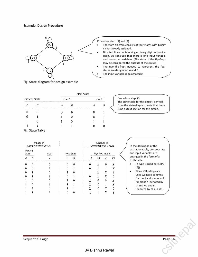
Sequential Logic Page 16
Example: Design Procedure
Fig: State-diagram for design example
Fig: State Table
Procedure step: (1) and (2)
The state diagram consists of four states with binary values already assigned.
Directed lines contain single binary digit without a slash, we conclude that there is one input variable and no output variables. (The state of the flip-flops may be considered the outputs of the circuit).
The two flip-flops needed to represent the four states are designated A and B.
The input variable is designated x.
Procedure step: (3) The state table for this circuit, derived from the state diagram. Note that there is no output section for this circuit.
In the derivation of the excitation table, present state and input variables are arranged in the form of a truth table.
JK type is used here. (PS (6))
Since JK flip-flops are used we need columns for the J and K inputs of flip-flops A (denoted by JA and KA) and B
(denoted by JB and KB).
csitn
epal
By Bishnu Rawal

Sequential Logic Page 17
Shows the two JK flip-flops needed for the circuit and a box to represent the combinational circuit. From the block diagram, it is clear that the outputs of the combinational circuit go to flip-flop inputs and external outputs (if specified). The inputs to the combinational circuit are the external inputs and the present state values of the flip-flops.
Derivation of simplified Boolean functions for the combinational circuit.
The information from the truth table is transferred into the maps.
The inputs are the variables A, B, and x; the outputs are the variables JA, KA, JB, and KB.
The logic diagram is drawn in by side and consists of two flip-flops, two AND gates, one exclusive-NOR gate, and one inverter.
csitn
epal
By Bishnu Rawal

Registers, Counters and Memory units Page 1
Unit 7 Registers, Counters and Memory units
A circuit with only flip-flops is considered a sequential circuit even in the absence of combinational gates. Certain MSI circuits that include flip-flops are classified by the operation that they perform rather than the name sequential circuit. Two such MSI components are registers and counters.
Registers
A register is a group of binary cells suitable for holding binary information. A group of flip-flops constitutes a register.
An n-bit register has a group of n flip-flops and is capable of storing any binary information containing n bits.
In addition to the flip-flops, a register may have combinational gates that perform certain data-processing tasks.
Various types of registers are available in MSI circuits. The simplest possible register is one that consists of only flip-flops without any external gates. Following fig. shows such a register constructed with four D-type flip-flops and a common clock-pulse input.
The clock pulse input, CP, enables all flip-flops, so that the information presently available at the four inputs can be transferred into the 4-bit register.
The four outputs can be sampled to obtain the information presently stored in the register.
Fig: 4-bit register
Register with parallel load The transfer of new information into a register is referred to as loading the register. If all the bits of the register are loaded simultaneously with a single clock pulse, we say that the loading is done in parallel. A pulse applied to the CP input of the register of Fig. above will load all four inputs in parallel. When CP goes to 1, the input information is loaded into the register. If CP remains at 0, the content of the register is not changed. Note that the change of state in the outputs occurs at the positive edge of the pulse.
Shift Registers A register capable of shifting its binary information either to the right or to the left is called a
shift register. The logical configuration of a shift register consists of a chain of flip-flops connected in cascade, with the output of one flip-flop connected to the input of the next flip-flop. All flip-flops receive a common clock pulse that causes the shift from one stage to the next.
The Shift Register is used for data storage or data movement and are used in calculators or computers to store data such as two binary numbers before they are added together, or to convert the data from either a serial to parallel or parallel to serial format. The individual data
csitn
epal
By Bishnu Rawal

Registers, Counters and Memory units Page 2
latches that make up a single shift register are all driven by a common clock (Clk) signal making them synchronous devices. Shift register IC's are generally provided with a clear or reset connection so that they can be "SET" or "RESET" as required.
Generally, shift registers operate in one of four different modes with the basic movement of data through a shift register being:
Serial-in to Parallel-out (SIPO) - the register is loaded with serial data, one bit at a time, with
the stored data being available in parallel form. Serial-in to Serial-out (SISO) - the data is shifted serially "IN" and "OUT" of the register, one bit
at a time in either a left or right direction under clock control. Parallel-in to Serial-out (PISO) - the parallel data is loaded into the register simultaneously and
is shifted out of the register serially one bit at a time under clock control. Parallel-in to parallel-out (PIPO) - the parallel data is loaded simultaneously into the register,
and transferred together to their respective outputs by the same clock pulse. The effect of data movement from left to right through a shift register can be presented graphically as:
Also, the directional movement of the data through a shift register can be either to the left, (left shifting) to the right, (right shifting) left-in but right-out, (rotation) or both left and right shifting within the same register thereby making it bidirectional.
Serial-in to Parallel-out (SIPO)
Fig: 4-bit Serial-in to Parallel-out Shift Register
csitn
epal
By Bishnu Rawal

Registers, Counters and Memory units Page 3
Operation
Let’s assume that all the flip-flops (FFA to FFD) have just been RESET (CLEAR input) and that all the outputs QA to QD are at logic level "0" i.e., no parallel data output.
If a logic "1" is connected to the DATA input pin of FFA then on the first clock pulse the output of FFA and therefore the resulting QA will be set HIGH to logic "1" with all the other outputs still remaining LOW at logic "0".
Assume now that the DATA input pin of FFA has returned LOW again to logic "0" giving us one data pulse or 0-1-0.
The second clock pulse will change the output of FFA to logic "0" and the output of FFB and QB HIGH to logic "1" as its input D has the logic "1" level on it from QA. The logic "1" has now moved or been "shifted" one place along the register to the right as it is now at QA. When the third clock pulse arrives this logic "1" value moves to the output of FFC (Q ) and so on until the arrival of the fifth clock pulse which sets all the outputs QA to QD back again to logic level "0" because the input to FFA has remained constant at logic level "0".
The effect of each clock pulse is to shift the data contents of each stage one place to the right, and this is shown in the following table until the complete data value of 0-0-0-1 is stored in the register.
Commonly available SIPO IC's include the standard 8-bit 74LS164 or the 74LS594.
Serial-in to Serial-out (SISO) This shift register is very similar to the SIPO above, except were before the data was read directly in a parallel form from the outputs QA to QD, this time the data is allowed to flow straight through the register and out of the other end. Since there is only one output, the DATA leaves the shift register one bit at a time in a serial pattern, hence the name Serial-in to Serial-Out Shift Register or SISO. The SISO
csitn
epal
By Bishnu Rawal

Registers, Counters and Memory units Page 4
shift register is one of the simplest of the four configurations as it has only three connections, the serial input (SI) which determines what enters the left hand flip-flop, the serial output (SO) which is taken from the output of the right hand flip-flop and the sequencing clock signal (Clk). The logic circuit diagram below shows a generalized serial-in serial-out shift register.
Fig: 4-bit Serial-in to Serial-out Shift Register
What's the point of a SISO shift register if the output data is exactly the same as the input data? Well this type of Shift Register also acts as a temporary storage device or as a time delay device for the data, with the amount of time delay being controlled by the number of stages in the register, 4, 8, 16 etc or by varying the application of the clock pulses. Commonly available IC's include the 74HC595 8-bit Serial-in/Serial-out Shift Register all with 3-state outputs.
Parallel-in to Serial-out (PISO) The Parallel-in to Serial-out shift register acts in the opposite way to the serial-in to parallel-out one above. The data is loaded into the register in a parallel format i.e. all the data bits enter their inputs simultaneously, to the parallel input pins PA to PD of the register. The data is then read out sequentially in the normal shift-right mode from the register at Q representing the data present at PA to PD. This data is outputted one bit at a time on each clock cycle in a serial format. It is important to note that with this system a clock pulse is not required to parallel load the register as it is already present, but four clock pulses are required to unload the data.
Fig: 4-bit Parallel-in to Serial-out Shift Register
Advantage: As this type of shift register converts parallel data, such as an 8-bit data word into serial format, it can be used to multiplex many different input lines into a single serial DATA stream which can be sent directly to a computer or transmitted over a communications line. Commonly available IC's include the 74HC166 8-bit Parallel-in/Serial-out Shift Registers.
Parallel-in to Parallel-out (PIPO) The final mode of operation is the Parallel-in to Parallel-out Shift Register. This type of register also acts as a temporary storage device or as a time delay device similar to the SISO configuration above. The data is presented in a parallel format to the parallel input pins PA to PD and then transferred together directly to their respective output pins QA to QD by the same clock pulse. Then one clock pulse loads and unloads the register. This arrangement for parallel loading and unloading is shown below.
csitn
epal
By Bishnu Rawal

Registers, Counters and Memory units Page 5
Fig: 4-bit Parallel-in to Parallel-out Shift Register
The PIPO shift register is the simplest of the four configurations as it has only three connections, the parallel input (PI) which determines what enters the flip-flop, the parallel output (PO) and the sequencing clock signal (Clk). Similar to the Serial-in to Serial-out shift register, this type of register also acts as a temporary storage device or as a time delay device, with the amount of time delay being varied by the frequency of the clock pulses. Also, in this type of register there are no interconnections between the individual flip-flops since no serial shifting of the data is required.
Ripple Counters (Asynchronous Counters)
MSI counters come in two categories: ripple counters and synchronous counters.
In a ripple counter (Asynchronous Counter); flip-flop output transition serves as a source for triggering other flip-flops. In other words, the CP inputs of all flip-flops (except the first) are triggered not by the incoming pulses, but rather by the transition that occurs in other flip-flops.
Synchronous counter, the input pulses are applied to all CP inputs of all flip-flops. The change of state of a particular flip-flop is dependent on the present state of other flip-flops.
Binary Ripple Counter A binary ripple counter consists of a series connection of complementing flip-flops (T or JK type), with the output of each flip-flop connected to the CP input of the next higher-order flip-flop. The flip-flop holding the least significant bit receives the incoming count pulses. The diagram of a 4-bit binary ripple counter is shown in Fig. below. All J and K inputs are equal to 1.
csitn
epal
By Bishnu Rawal

Registers, Counters and Memory units Page 6
Fig: 4-bit binary ripple counter
All J and K inputs are equal to 1. The small circle in the CP input indicates that the flip-flop complements during a negative-going transition or when the output to which it is connected goes from 1 to 0.
To understand the operation of the binary counter, refer to its count sequence given in Table.
It is obvious that the lowest-order bit A1 must be complemented with each count pulse. Every time A1 goes from 1 to 0, it complements A2. Every time A2 goes from 1 to 0, it complements A3, and so on.
For example: take the transition from count 0111 to 1000. The arrows in the table emphasize the transitions in this case. A1 is complemented with the count pulse. Since A1 goes from 1 to 0, it triggers A2 and complements it. As a result, A2 goes from 1 to 0, which in turn complements A3. A3 now goes from 1 to 0, which complements A4. The output transition of A4, if connected to a next stage, will not trigger the next flip-flop since it goes from 0 to 1. The flip-flops change one at a time in rapid succession, and the signal propagates through the counter in a ripple fashion.
csitn
epal
By Bishnu Rawal

Registers, Counters and Memory units Page 7
BCD Ripple Counter (Decade Counter) A decimal counter follows a sequence of ten states and returns to 0 after the count of 9. Such a counter must have at least four flip-flops to represent each decimal digit, since a decimal digit is represented by a binary code with at least four bits. The sequence of states in a decimal counter is dictated by the binary code used to represent a decimal digit.
Fig: BCD ripple counter BCD Counter above counts from 0 to 9. To count in decimal from 0 to 99, we need a two-decade counter. To count from 0 to 999, we need a three-decade counter.
If BCD is used, the sequence of states is as shown in the state diagram. This is similar to a binary counter, except that the state after 1001 (code for decimal digit 9) is 0000 (code for decimal digit 0).
The four outputs are designated by the letter symbol Q with a numeric subscript equal to the binary weight of the corresponding bit in the BCD code.
The flip-flops trigger on the negative edge.
A ripple counter is an asynchronous sequential circuit and cannot be described by Boolean equations developed for describing clocked sequential circuits. Signals that affect the flip-flop transition depend on the order in which they change from 1 to 0.
Operation: When CP input goes from 1 to 0, the flip-flop is set if J = 1, is cleared if K = 1, is complemented if J = K = 1, and is left unchanged if J = K = 0. The following are the conditions for each flip-flop state transition: 1. Q1 is complemented on the negative edge
of every count pulse. 2. Q2 is complemented if Q8 = 0 and Q1 goes
from 1 to 0. Q2 is cleared if Q8 = 1 and Q1 goes from 1 to 0.
3. Q4 is complemented when Q2 goes from 1 to 0.
4. Q8 is complemented when Q4 Q2 = 11 and Q1 goes from 1 to 0. Q8 is cleared if either Q4 or Q2 is 0 and Q1 goes from 1 to 0.
csitn
epal
By Bishnu Rawal

Registers, Counters and Memory units Page 8
Fig: Block diagram of a three-decade decimal BCD counter
Synchronous Counters Synchronous counters are distinguished from ripple counters in that clock pulses are applied to the CP inputs of all flip-flops. The common pulse triggers all the flip-flops simultaneously, rather than one at a time in succession as in a ripple counter. The decision whether a flip-flop is to be complemented or not is determined from the values of the J and K inputs at the time of the pulse. If J = K = 0, the flip-flop remains unchanged. If J = K = 1, the flip-flop complements.
Binary Counter
Fig: 4-bit Synchronous Binary Counter
Multiple-decade counters can be constructed by connecting BCD counters in cascade, one
for each decade.
The design of synchronous binary counters is so simple that there is no need to go through a rigorous sequential-logic design process. In a synchronous binary counter, the flip-flop in the lowest-order position is complemented with every pulse. This means that it’s J and K inputs must be maintained at logic-1. A flip-flop in any other position is complemented with a pulse provided all the bits in the lower-order positions are equal to 1, because the lower-order bits (when all 1's) will change to 0's on the next count pulse.
Synchronous binary counters have a regular pattern and can easily be constructed with complementing flip-flops and gates. The regular pattern can be clearly seen from the 4-bit counter depicted in Fig by side.
The CP terminals of all flip-flops are connected to a common clock-pulse source. The first stage A1 has its J and K equal to 1 if the counter is enabled. The other J and K inputs are equal to 1 if all previous low-order bits are equal to 1 and the count is enabled. The chain of AND gates generates the required logic for the J and K inputs in each stage. The counter can be extended to any number of stages, with each stage having an additional flip-flop and an AND gate that gives an output of 1 if all previous flip-flop outputs are 1's.
csitn
epal
By Bishnu Rawal

Registers, Counters and Memory units Page 9
Binary Up-Down Counter
Fig: 4-bit up-down counter
BCD Counter A BCD counter counts in binary-coded decimal from 0000 to 1001 and back to 0000. Because of the return to 0 after a count of 9, a BCD counter does not have a regular pattern as in a straight binary count. To derive the circuit of a BCD synchronous counter, it is necessary to go through a design procedure discussed earlier. The excitation for the T flip-flops is obtained from the present and next state conditions. An output y is also shown in the table. This output is equal to 1 when the counter present state is 1001. In this way, y can enable the count of the next-higher-order decade while the same pulse switches the present decade
In a synchronous count-down binary counter, the flip-flop in the lowest-order position is complemented with every pulse. A flip-flop in any other position is complemented with a pulse provided all the lower-order bits are equal to 0.
Example: if the present state of a 4-bit count-down binary counter is A4A3A2A1 = 1100, the next count will be 1011. A1 is always complemented. A2 is complemented because the present state of A1 = 0. A3 is complemented because the present state of A2A1 = 00. But A4 is not complemented because the present state of A3A2A1 = 100, which is not an all-0's condition.
Same as Binary counter except that the inputs to the AND gates must come from the complement outputs Q' and not from the normal outputs Q of the previous flip-flops.
The two operations can be combined in one circuit. A binary counter capable of counting either up or down is shown in Fig. by side.
o When up = 1, the circuit counts up, since the T inputs receive their signals from the values of the previous normal outputs of the flip-flops.
o When down = 1 and up = 0, the circuit counts down
csitn
epal
By Bishnu Rawal

Registers, Counters and Memory units Page 10
from 1001 to 0000. The flip-flop input functions from the excitation table can be simplified by means of maps. The unused states for minterms 10 to 15 are taken as don't-care terms.
The simplified functions are: TQ1 = 1 TQ2 = Q8’Q1 TQ4 = Q2Q1 TQ8 = Q8Q1 + Q4Q2Q1 y = Q8Q1
The circuit can be easily drawn with four T flip-flops, five AND gates, and one OR gate. Synchronous BCD counters can be cascaded to form a counter for decimal numbers of any length.
Timing Sequences
The sequences of operations in a digital system are specified by a control unit. The control unit that supervises the operations in a digital system would normally consist of timing signals that determine the time sequence in which the operations are executed. The timing sequences in the control unit can be easily generated by means of counters or shift registers. Word-Time Generation The control unit in a serial computer must generate a word-time signal that stays on for a number of pulses equal to the number of bits in the shift registers. The word-time signal can be generated by means of a counter that counts the required number of pulses. Example:
Assume that the word-time signal to be generated must stay on for a period of eight clock pulses.
Fig. shows a counter circuit that accomplishes this task.
Initially, the 3-bit counter is cleared to 0. A start signal will set flip-flop Q. The output of this flip-flop supplies the word-time control and also enables the counter. After the count of eight pulses, the flip-flop is reset and Q goes to 0.
csitn
epal
By Bishnu Rawal

Registers, Counters and Memory units Page 11
Timing Signals The control unit in a digital system that operates in the parallel mode must generate timing signals that stay on for only one clock pulse period. Timing signals that control the sequence of operations in a digital system can be generated with a shift register or a counter with a decoder. A ring counter is a circular shift register with only one flip-flop being set at any particular time; all others are cleared. The single bit is shifted from one flip-flop to the other to produce the sequence of timing signals.
Fig: Generation of Timing Signals
The timing diagram demonstrates the operation of the circuit. The start signal is synchronized with the clock and stays on for one clock-pulse period. After Q is set to 1, the counter starts counting the clock pulses. When the counter reaches the count of 7 (binary 111), it sends a stop signal to the reset input of the flip-flop. The stop signal becomes a 1 after the negative-edge transition of pulse 7. The next clock pulse switches the counter to the 000 state and also clears Q. Now the counter is disabled and the word-time signal stays at 0.
Figure (a) shows a 4-bit shift register connected as a ring counter. The initial value of the register is 1000, which produces the variable T0. The single bit is shifted right with every clock pulse and circulates back from T3 to T0. Each flip-flop is in the 1 state once every four clock pulses and produces one of the four timing signals shown in Fig (c). Each output becomes a 1 after the negative-edge transition of a clock pulse and remains 1 during the next clock pulse.
The timing signals can be generated also by continuously enabling a 2-bit counter that goes through four distinct states. The decoder shown in Fig. (b) decodes the four states of the counter and generates the required sequence of timing signals.
csitn
epal
By Bishnu Rawal

Registers, Counters and Memory units Page 12
Point!
To generate 2n timing signals, we need either a shift register with 2n flip-flops or an n-bit counter
together with an n-to-2n-line decoder. For example, 16 timing signals can be generated with a 16-bit
shift register connected as a ring counter or with a 4-bit counter and a 4-to-16-line decoder.
It is also possible to generate the timing signals with a combination of a shift register and a decoder. In this way, the number of flip-flops is less than a ring counter, and the decoder requires only 2-input gates. This combination is sometimes called a Johnson counter. (Oh ya, we r studying it in what follows…)
Johnson Counter A Johnson counter is a k-bit switch-tail ring counter with 2k decoding gates to provide outputs for 2k timing signals.
Fig: Construction of a Johnson counter
The eight AND gates listed in the table, when connected to the circuit will complete the construction of the Johnson counter. Since each gate is enabled during one particular state sequence, the outputs of the gates generate eight timing sequences in succession. Operation: The decoding of a k-bit switch-tail ring counter to obtain 2k timing sequences follows a regular pattern. The all-0’s state is decoded by taking the complement of the two extreme flip-flop outputs. The all-1's state is decoded by taking the normal outputs of the two extreme flip-flops. All other states are decoded from an adjacent 1, 0 or 0, 1 pattern in the sequence. For example, sequence 7 has an adjacent 0, 1 pattern in flip-flops B and C. The decoded output is then obtained by taking the complement of B and the normal output of C, or B' C. Johnson counters can be constructed for any number of timing sequences. The number of flip-flops
needed is one-half the number of timing signals. The number of decoding gates is equal to the number of timing signals and only 2-input gates are employed.
A switch-tail ring counter is a circular shift register with the complement output of the last flip-flop connected to the input of the first flip-flop.
A k-bit ring counter circulates a single bit among the flip-flops to provide k distinguishable states.
The number of states can be doubled if the shift register is connected as a switch-tail ring counter.
csitn
epal
By Bishnu Rawal

Registers, Counters and Memory units Page 13
Memory unit (Random Access Memory-RAM) A memory unit is a collection of storage cells together with associated circuits needed to
transfer information in and out of the device. Memory cells can be accessed for information transfer to or from any desired random location and hence the name random access memory, abbreviated RAM.
A memory unit stores binary information in groups of bits called words. A word in memory is an entity of bits that move in and out of storage as a unit. A memory word is a group of 1's and 0's and may represent a number, an instruction, one or more alphanumeric characters, or any other binary-coded information.
Fig: Block Diagram of a memory unit
Conventions for Memory storage:
K (kilo) = 210 M (mega) = 220 G (giga) = 230 Thus, 64K = 216, 2M = 221, and 4G = 232
Example: Memory unit with a capacity of 1K words of 16 bits each. Since 1K = 1024 = 210 and 16 bits constitute two bytes, we can say that the memory can accommodate 2048 = 2K bytes.
Fig: Possible content of 1024 x 16 memory
The communication between a memory and its environment is achieved through:
o n data input lines : provide information to be stored in memory
o n data output lines: supply the information coming out of memory.
o k address lines: specify particular word chosen among the many available.
o two control inputs: specify the direction of transfer desired
Each word in memory is assigned an identification number, called an address, starting from 0 and continuing with 1, 2, 3, up to 2k - I, where k is the number of address lines.
Computer memories may range from 1024 words, requiring an address of 10 bits, to 232 words, requiring 32 address bits.
Each word contains 16 bits, which can be divided into two bytes. The words are recognized by their decimal address from 0 to 1023. The equivalent binary address consists of 10 bits. The first address is specified with ten 0's, and the last address is specified with ten 1's. A word in memory is elected by its binary address. When a word is read or written, the memory operates on all 16 bits as a single unit. Memory address register (MAR): It is CPU register which contains the address of the memory words. If memory has k address lines, then MAR is of k-bits. Memory Buffer Register (MBR): It contains the word-data pointed by the MAR.
csitn
epal
By Bishnu Rawal
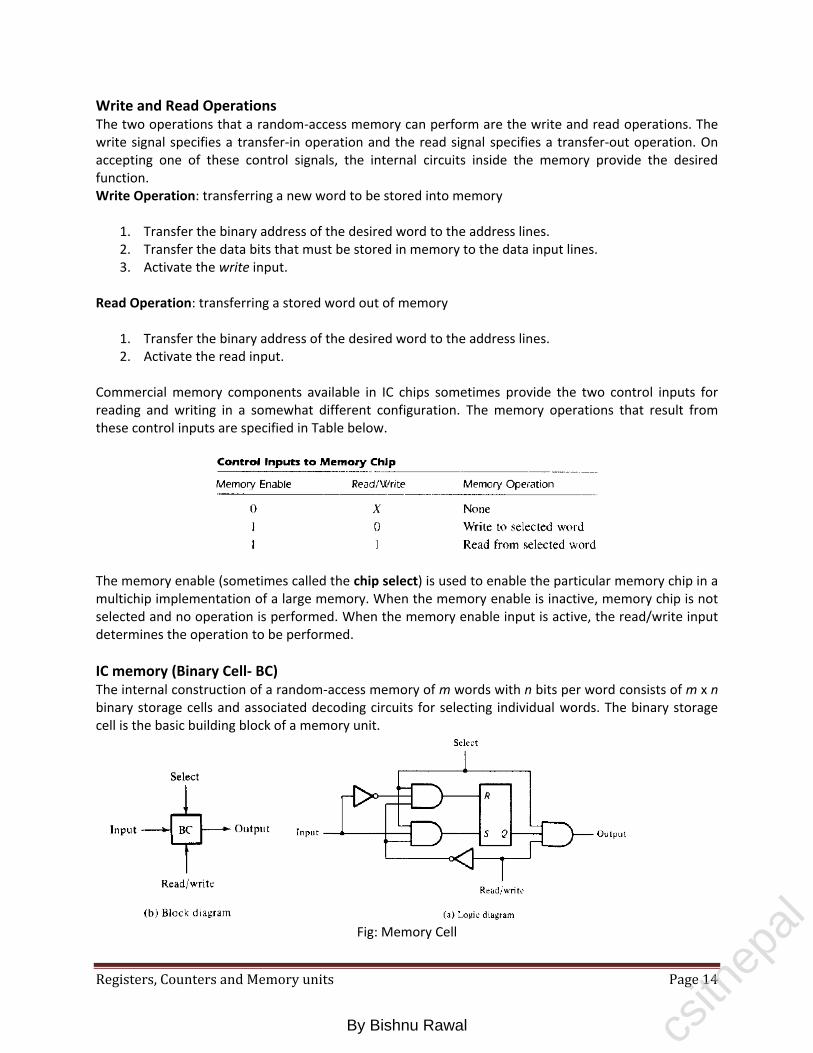
Registers, Counters and Memory units Page 14
Write and Read Operations The two operations that a random-access memory can perform are the write and read operations. The write signal specifies a transfer-in operation and the read signal specifies a transfer-out operation. On accepting one of these control signals, the internal circuits inside the memory provide the desired function. Write Operation: transferring a new word to be stored into memory
1. Transfer the binary address of the desired word to the address lines. 2. Transfer the data bits that must be stored in memory to the data input lines. 3. Activate the write input.
Read Operation: transferring a stored word out of memory
1. Transfer the binary address of the desired word to the address lines. 2. Activate the read input.
Commercial memory components available in IC chips sometimes provide the two control inputs for reading and writing in a somewhat different configuration. The memory operations that result from these control inputs are specified in Table below.
The memory enable (sometimes called the chip select) is used to enable the particular memory chip in a multichip implementation of a large memory. When the memory enable is inactive, memory chip is not selected and no operation is performed. When the memory enable input is active, the read/write input determines the operation to be performed.
IC memory (Binary Cell- BC) The internal construction of a random-access memory of m words with n bits per word consists of m x n binary storage cells and associated decoding circuits for selecting individual words. The binary storage cell is the basic building block of a memory unit.
Fig: Memory Cell
csitn
epal
By Bishnu Rawal


![Proof theory for hybrid(ised) logics I - COnnecting REpositories · 2019. 10. 24. · logics [7], quantum logics [13], hidden and observational logics [11, 9, 43], algebrocaic logics](https://img.pdfslide.net/doc/110x75/6125029257792013567e5d86/proof-theory-for-hybridised-logics-i-connecting-repositories-2019-10-24.jpg)