Embed Size (px)
Citation preview

1
Conference Project Proceedings
„Institut experimentálních technologií 2“
20th – 21st September, 2011 Brno, Czech Republic
Project funding is provided by the European Social Fund and the national budget of the Czech Republic.

2
Editor doc. Ing. Pavel Fiala, Ph.D., Ing. Jan Mikulka Title Conference proceedings of the Project „Institut experimentálních technologií 2“ Issue first Year of publication 2011 Publisher Brno University of Technology, Faculty of Electrical Engineering and
Communication Print Entity Production, Ltd. ISBN 978-80-214-4315-0

3
Conference of the project „Institut experimentálních technologií 2“
Chairman doc. Ing. Pavel Fiala, Ph.D., BUT, Czech Republic
Technical program commitee
prof. Ing. Karel Bartušek, DrSc., BUT, Czech Republic prof. Ing. Jarmila D�dková, CSc., BUT, Czech Republic
prof. Dr. Ulrich Schmid, Vienna University of Technology, Austria Dr. Beata Mikovicova, Institut Supérieur d’Electronique de Paris, France
Ing. Frederic Amiel, Institut Supérieur d’Electronique de Paris, France Dr. Dieudonne Abboud, Institut Supérieur d’Electronique de Paris, France
doc. Ing. Petr Drexler, Ph.D., BUT, Czech Republic doc. Ing. Petr Ko�as, Ph.D. , BUT, Czech Republic doc. Ing. Pavel Fiala, Ph.D., BUT, Czech Republic Ing. Radek Kubásek, Ph.D., BUT, Czech Republic
Ing. Michal Hadinec, BUT, Czech Republic Ing.Tomáš K�íž, BUT, Czech Republic
Ing. Zden�k Roubal, BUT, Czech Republic Ing. Radim Kadlec, BUT, Czech Republic Ing. Jan Mikulka, BUT, Czech Republic Ing. Zoltán Szabó, BUT, Czech Republic Ing. Martin Friedl, BUT, Czech Republic
Ing. Tibor Bachorec, Ph.D., SVS FEM Ltd., Czech Republic Ing. Michal Král, Prototypa a.s., Czech Republic
Ing. Pavel Vá�o, ABB Ltd., Czech Republic Ing. Radek Javora, Ph.D., ABB Ltd., Czech Republic
Ing. Petr Slavata, Eaton Elektrotechnika Ltd., Czech Republic Ing. Jind�ich Bulva, Eaton Elektrotechnika Ltd., Czech Republic
Organisation committee Ing. Ta�ána Kraj�írovi�ová, BUT, Czech Republic
Marie Hábová, BUT, Czech Republic

4
Content CONTENT ................................................................................................................................. 4 INTRODUCTION ...................................................................................................................... 5 INSTITUTE OF EXPERIMENTAL TECHNOLOGY ............................................................. 7 FACULTY OF ELECTRICAL ENGINEERING AND COMMUNICATION ...................... 11 EATON ELEKTROTECHNIKA LTD. ................................................................................... 14 SVS FEM LTD. ........................................................................................................................ 16 ABB IN THE CZECH REPUBLIC ......................................................................................... 17 PROTOTYPA A.S. .................................................................................................................. 22 MEASURING THE ATTRIBUTES OF LASER SOURCE WITH CYLINDRICAL LENS . 25 METAL DETECTORS ............................................................................................................ 28 ROBOTIC CHASSIS ............................................................................................................... 31 PROGRAMMABLE INDUSTRIAL CONTROLLER ............................................................ 34 SPECIAL SENSORS FOR SENSING FAST ONE-TIME EVENTS ..................................... 36 MAGNETIC FIELDS MAPPING OF SPECIFIC CONFIGURATIONS ............................... 40 VERIFICATION OF DURABILITY AND RELIABILITY OF ELECTRONIC MODULES AND ACCELERATED TESTS ............................................................................................... 43 DESIGN OF MEASUREMENT NET ..................................................................................... 46 PREPARATION OF ENGINEERING DRAWINGS FOR DEVICES DATABASE ............. 49 DESIGN OF LOW VOLTAGE SWITCHGEAR .................................................................... 52 SIGNAL ANALYSIS FOR STIMULATION OF BIOLOGICAL OBJECTS ........................ 55 PRACTICAL IMPLEMENTATIO OF NOISE GENERATOR .............................................. 58 SENSORS FOR SHORT HIGH LEVEL CURRENT IMPULSE ........................................... 60 AUTOMATIC TEST LINE SUGGESTION ........................................................................... 63 OPTIMIZATION OF METHODS FOR IMAGE NOISE SUPPRESSION ............................ 66 DESIGN OF MAGNETIC BAR-CODE READ HEAD .......................................................... 70 NUMERICAL MODELING OF MAGNETIC SUSCEPTIBILITY ON MR IMAGES ......... 73 DESIGN OF WIRELESS SIGNAL TRANSMISION FROM THERMAL SENSORS ......... 76 THE CONSTRUCTION AND DESIGN A TRANSFORMER .............................................. 80 MEASURING BOX WITH PELTIER CELLS ...................................................................... 83 CONTROL SPECIAL AUTOMATS ....................................................................................... 86 WIRELESS REMOTE CONTROL WITH A CODED TRANSMISSION ............................ 89 ATMOSPHERIC CORRECTION UNIT FOR LASER INTERFEROMETER ..................... 92
5
Introduction Both small nations and small companies often find it difficult to specialize intensively Bohumil Kral, M.Eng, CSc. PROTOTYPA a.s. Motto: .... A small nation often finds it difficult to specialize intensively. During the prewar period, the current standard of education would have been adequate. But today there is an ever increasing need to provide a broader basis for our knowledge. And it is here that I feel that the French orientation toward scientific study is worth noting. French science is characterized by a kind of generality. It expresses a love for fundamental phenomena and simplicity. Such an orientation, adapted to conform to our natural disposition, may serve as the basis for the technical work of our engineers, allowing them to easily accommodate their work demands. Some of our universities have introduced specialized fields. But this specialization is in no way in conflict with what has been said above. To the contrary, the introduction of specialization was a masterful step which captured the requirements of its time. An electrician, used to alternating phenomena, well understands that all cultural development takes place via regular oscillations. And so specialization was introduced during the period of oscillation in which the development of science required separation. Today, however, another oscillatory period is coming which demands a certain degree of generality. Thus my comments. I'm not sure whether it's here yet but I am confident that further oscillations will ensue requiring further specialization and then, once again, more generality – and we will be unaware which of the two will constitute the final stage of development. [1] These words were written by the 28-year-old Ales Blaha in 1934. Blaha later became a professor and head of the Institute of Theoretical and Experimental Electrical Engineering, the same institution which today oversees the IET1 and IET2 projects. The methodological training Bláha emphasized, its validity demonstrated by the experience of the French, allows the structure of the problem to be determined, its solution predicted and its particularities and differences revealed. One can thus view the matter in the context of a number of other problems. This leaves fewer methodological procedures (perhaps only a single such procedure in its highest form). A head thus shaped can think clearly and economically and, of course, most intensively. There is the chance to solve every new problem not covered in the manual. This methodical, dynamic component of thinking, which forms the basis of creative work, may be obtained only by continuous exercise. When the focus turns to education and awareness, only effort retains any value. ... Effort is what is needed. Effort makes spirit stronger and improves it. It is discipline in effort which allows a person to aim ever higher and face ever greater trials. It is this methodological training, in my estimation, which is what our students and engineers are missing, the art of efficiently aiming ever higher, and it is missing in both the secondary schools and the universities. .... The point is to teach students to create independently and methodically, to inspire them with the experience they need to deal with the problem. This experience will prove its worth. Later, in their engineering courses, they will be able to work vigorously and confidently, saving time and showing a high degree of originality .... Engineering work is scientific work and the methodology behind scientific work is basically identical .. [1] I must say his words are as current today, in 2011, as they were then – for small businesses with their own development, they are downright prophetic. A future electrical engineer hired by PROTOTYPA Plc.– a company with around 20 employees and a maximum five-member team devoted to development – should have a broad theoretical and experimental education and be able to adapt to multidisciplinary projects and, in the course of time, master new skills and come up with original ideas. In particular, the candidate should have a good
6
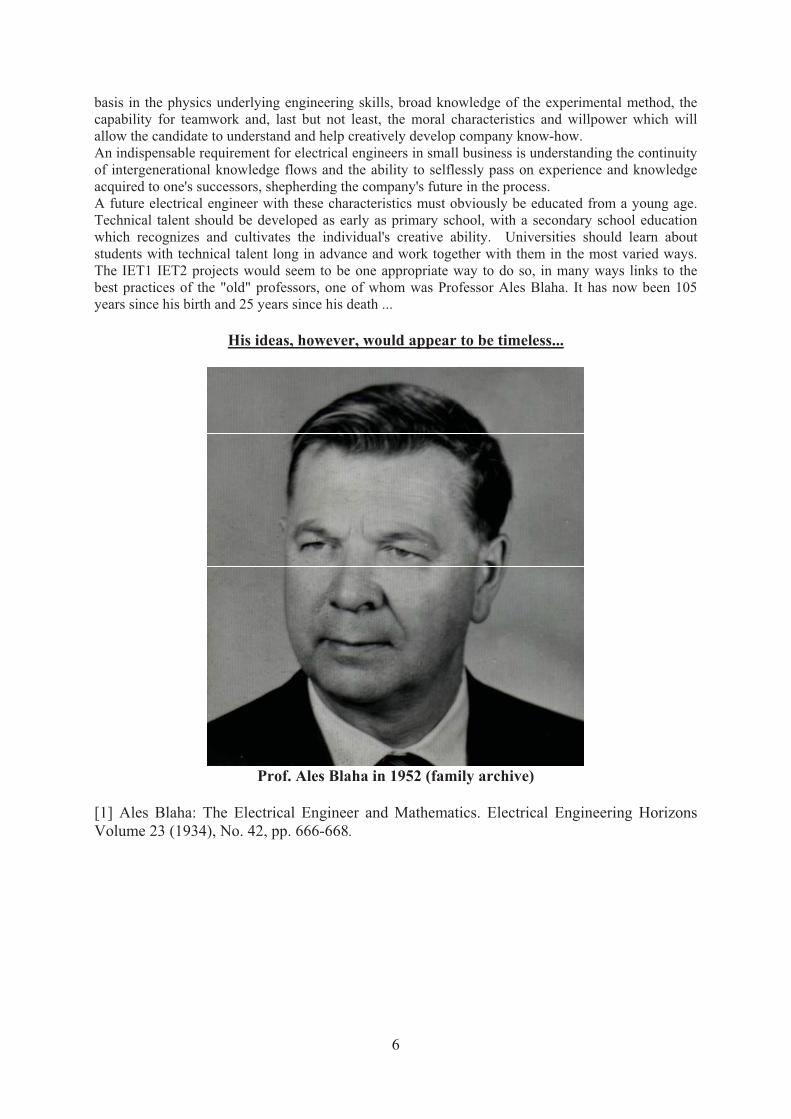
basis in the physics underlying engineering skills, broad knowledge of the experimental method, the capability for teamwork and, last but not least, the moral characteristics and willpower which will allow the candidate to understand and help creatively develop company know-how. An indispensable requirement for electrical engineers in small business is understanding the continuity of intergenerational knowledge flows and the ability to selflessly pass on experience and knowledge acquired to one's successors, shepherding the company's future in the process. A future electrical engineer with these characteristics must obviously be educated from a young age. Technical talent should be developed as early as primary school, with a secondary school education which recognizes and cultivates the individual's creative ability. Universities should learn about students with technical talent long in advance and work together with them in the most varied ways. The IET1 IET2 projects would seem to be one appropriate way to do so, in many ways links to the best practices of the "old" professors, one of whom was Professor Ales Blaha. It has now been 105 years since his birth and 25 years since his death ...
His ideas, however, would appear to be timeless...
Prof. Ales Blaha in 1952 (family archive)
[1] Ales Blaha: The Electrical Engineer and Mathematics. Electrical Engineering Horizons Volume 23 (1934), No. 42, pp. 666-668.
7
Institute of Experimental Technology Pavel Fiala, PhD The Institute of Experimental Technology (IET, a registered trademark, www.ietbrno.eu) was set up on January 1, 2008 at the Institute of Theoretical and Experimental Electrical Engineering of the Faculty of Electrical Engineering and Communication at BUT, with the chief goal of preparing talented students for excellence in the labor market. A secondary, but still significant goal, is to promote the discipline and convince young people to study electrical engineering. The Institute is a modern educational facility whose key educational methodology involves working with student teams under the directorship of PhD students and young academics on top-level projects submitted by industrial firms, rather than confining the students to working only on education-based themes. We have been able to place students from both the polytechnical university and secondary schools on the teams. We have been able to heighten the competency of graduates of technically-oriented secondary schools and grammar schools, as well as universities, to orient them to keep pace with trends in innovation and keep in line with the direction of development in the electrical technology industry in the CR of the 21st century. The development of this seemingly simple idea has been tied to the tradition of the Institute of Theoretical and Experimental Electrical Engineering led by Prof. Ales Blaha during the postwar era. Meetings with the Department of Education of the Southern Moravian Region, Brno City Hall and the Brno Regional Chamber of Commerce provided the inspiration and support for reinvigorating this method of instruction. All of these institutions fear a permanent, deepening shortage of qualified employees in the technical disciplines at all levels. We all see it as a dangerous signal for the future of the region. Thus the project of the Institute of Experimental Technology was begun, with support from the Ministry of Education, Youth and Sports of the CR (MEYS), with which we have joined forces in deciding to contribute to finding a remedy for this unfortunate state of affairs. Our experience confirms that the search for talented young people must begin in the elementary schools. We have therefore sought cooperation in finding talented students and preparing them for study in the technical disciplines at all competent educational institutions aware of the importance of quality technical preparation and of the need to develop the talent of gifted students – not only for their personal career purposes, but for the competitiveness of Czech industry, as well. Implementation of the Institute of Experimental Technology 2 project, supported by MEYS under the European Structural Funds of Priority Axis 2.2 OP Education for Competitiveness, has allowed secondary schools in the region to enjoy the benefits of a number of activities targeting expansion of the professional competency of teaching staff. These activities have also served to promote the technical sciences and support technical education. Contacts were established with electrical engineering enterprises in the CR. The Institute is ready to further expand, deepen and develop cooperation with research teams at electrical engineering firms and, secondarily, to provide for the exchange of experience between schools at all levels and establish dynamic contacts with emerging companies in the exciting, rapidly-developing field of electrical engineering whose management is enlightened and far-sighted. To provide for the Institute's activities, we apply for various forms of targeted support. A few words and facts about the IET2 CZ.1.07/2.2.00/07.0390 project. The planned timeframe for the project is 1/3/2009-29/2/2013. But right at its inception, the funding provider forced a delay and after some considerable effort, the project got underway on June 1, 2009. This slight postponement of the start date require that the entire project be redone, since the timetable for the work and coordination of activities was synchronized in the original project with the academic year at Brno University of Technology. The entire project structure had to be adapted and reworked, from the budget to key closing activities. Project Objectives The educational and research activities of the Institute of Experimental Technology 2 (IET2) are focused on preparing highly qualified specialists for the needs of industry. This is a

8
novel, unique instructional system based upon a combination of classical methodology, maximum use of ICT technology for instruction, self-study on the part of talented students and work on real-life projects submitted by industrial firms. This creative collaboration will lead to tighter connections between tertiary education and industry. The IET2 project further targets involving other students of FEEC VUT Brno in industrial projects (especially their calculation/numerical sections), since these skills will be required of graduates in practice. For this reason, an innovation will be introduced into the educational program which will see a new subject of study entitled Modeling Electromagnetic Fields, in both the bachelors (BMEF) and masters (MMEF) programs. This innovation is necessary, both because of rapid changes in the way modeling and numerical calculations take place and in reaction to requirements by companies concerning the quality of entry-level knowledge of polytechnical graduates entering the job market. All projects submitted to IET for work by student teams will contain a theoretical/research section, calculation-based/numerical section and concluding-practical section which will contain output or implement prototypes which fulfill company requirements. The project will conclude with a defense before an IET committee composed of specialists in the field and academics. Internships will be secured for students in companies submitting projects. Academics themselves will also increase their knowledge of complex numerical calculations and be able to use that knowledge both in construction and in guiding student project teams. IET will be involved in international cooperation, with the goal of exchanging experience in innovating instructional modules. The demand for qualified graduates of universities in electrical engineering areas is growing, as is clear from a survey of its members conducted in 2006-2008 by the Association of Industry and Transport of the CR (AITCR). This offers universities the opportunity to support talented students in carrying out industrial projects and increasing the competitiveness of universities by introducing innovations in their programs of study and elevating the competency of academic specialists, with an eye to adapting the profile of technical university graduates most closely to the needs of industry. The IET2 project has demonstrated an innovative approach to the education and preparation of human resources at universities, thanks to tying theoretical knowledge to the practical environment provided by carrying out real-life projects submitted by industrial firms. Currently, university graduates are inadequately prepared to enter the job market – something which is once again evident from the AITCR survey. The profile does not correspond to the current needs of companies active in the CR or, indeed, in the EU at large. Working on real-life projects in teams, taking internships in industrial firms and receiving current information in one's education shorten the time needed to master one's professional tasks in employment. Graduates are equipped with practical skills and acquainted with the procedures used in the company at hand, increasing company productivity. The project aims to increase the competency of academic specialists so that they may thoroughly prepare students for the needs of the labor market. This emphasis on the practical skills of graduates of technical schools was discussed with Brno City Hall, the Education Department of the Southern Moravian Region, the Regional Chamber of Commerce and industrial firms, all of whom gave their support. At the end of the project, we can claim attainment of tighter ties between the academic and industrial spheres, increased specialist knowledge among students and academics in the electrical technology field and, in the final analysis, increased competitiveness for Czech industry. Project Benefits The IET2 project has provided academics with the opportunity to consult innovative programs of study with experts in the field, to enrich their instruction with practical examples and tasks, and to keep pace with the latest knowledge from the field, particularly as concerns interdisciplinary trends in current industrial development. Talented university students involved in industrial projects will make an easier transition to work or in assuming an academic career at the university level. Students receive the advantage of having direct contact with industrial firms submitting projects and with their experts. During project work, they acquire communication and team skills, the ability to make presentations and acquaint themselves with principles of project work, which vary widely by type of business and include meeting the needs of the project submitter – their potential employer. In their role as team leaders, doctoral students and their supervisors (academics fully responsible for the successful

9
management of projects) acquire managerial skills. IET's emphasis on uniting academic education and the needs of industry will lead to ever increasing specialist knowledge on the part of academics, resistance to stress and their direct connection to practice, including guiding students toward the practical use of theoretical knowledge acquired, from the very beginning of their studies. IET makes maximum use of the facilities offered by the university. A model laboratory was built to accommodate project work, providing a good laboratory environment for the practical portion of IET instruction. Innovation for the academic and student target group lies in a very close interconnection between instruction in the schools and reality in the industrial workplace. The material taught is not contained in a rigid package of information; rather, the entire teaching concept has been adapted to allow collaboration with leading experts from industry. The subject content of accredited courses has been flexibly updated to include the latest knowledge. Students are thus able to put the knowledge they have acquired to work on real-life issues. Activities after the Termination of ESF Funding After ESF funding for the IET2 project is complete, the BMEM study program will have been created and the MMEM program innovated. Curriculum and study support will be created and academics will have been trained to carry out instruction. Both subjects will continue to be offered under the bachelors and masters degree programs for a minimum of a further five years. At the same time, the programs will be further developed and feedback from students, instructors and experts in the field will be applied. New partnerships will be concluded with industrial firms who will take part in instruction and provide project submissions for work by student teams. Given that demand for taking part in three-week internships in firms is expected to be excessive, an attempt will be made to exponentially increase the number of partner firms providing internships, who will also have the chance to select and motivate potential employees to work at their companies. During the two-year course of work on a particular project, they will have an extraordinary opportunity to help train graduates in keeping with current trends. The submission of projects, consultation during the project itself, internships and defense under the guide of specialists at the company will all be treated in an economic agreement in which the firm provides these activities and which designates conditions under which IET student projects will take place. In implementing the IET2 project, project acquisition organizational mechanisms were created and introduced. Administrative processes supporting recordkeeping of projects, IET students and their project activities were prepared and implemented. The process for further education of academic staff which has been launched will continue with the assistance of company experts. The school/industry communications platform created will be used to further professional development. Other plans include expanding international collaboration with other partner organizations abroad, allowing for introduction of foreign student exchange programs. Collaboration with the French ISEP will continue and be expanded to include collaboration with TU Vienna at the pedagogical and didactic levels and in R&D projects. Methodological Innovation The innovative character and originality of the IET2 project lies in the actual introduction of an element which ties tertiary education to the needs of industrial firms as a part of the curriculum, as well as a focus on the profile of university graduates entering the job market. This is done uniquely by responsibly involving students in industrial projects during their studies and using a sophisticated system for the preparation of human resources. In addition to its benefits for students, IET also offers academic staff the opportunity to develop its competence. In combination with the IET1 project, both the tertiary area and the area of initial training receive consideration. Great emphasis is laid on successful project work by student project teams, maintaining deadlines and the quality requirements of firms. This requires the acquisition of project management principles, along with communication skills, including a particular business viewpoint. Place for the development of competency has been made in the course plans and training, with involvement in an international network (in the form of workshops and conferences). Via IET, students are guided to work with the system they will use upon entering the job market, i.e.: 1. studying the problem from available sources,
10
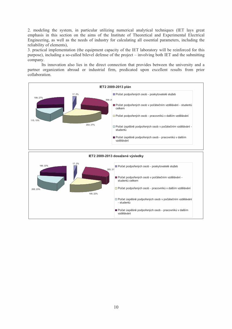
2. modeling the system, in particular utilizing numerical analytical techniques (IET lays great emphasis in this section on the aims of the Institute of Theoretical and Experimental Electrical Engineering, as well as the needs of industry for calculating all essential parameters, including the reliability of elements), 3. practical implementation (the equipment capacity of the IET laboratory will be reinforced for this purpose), including a so-called bilevel defense of the project – involving both IET and the submitting company. Its innovation also lies in the direct connection that provides between the university and a partner organization abroad or industrial firm, predicated upon excellent results from prior collaboration.
IET2 2009-2013 plán
17; 2%
209; 29%
203; 27%
115; 15%
199; 27%Po�et podpo�ených osob - poskytovatelé služeb
Po�et podpo�ených osob v po�áte�ním vzd�lávání - student�celkem
Po�et podpo�ených osob - pracovník� v dalším vzd�lávání
Po�et úsp�šn� podpo�ených osob v po�áte�ním vzd�lávání -student�
Po�et úsp�šn� podpo�ených osob - pracovník� v dalšímvzd�lávání
IET2 2009-2013 dosažené výsledky
17; 2%
265; 31%
195; 22%
205; 23%
195; 22% Po�et podpo�ených osob - poskytovatelé služeb
Po�et podpo�ených osob v po�áte�ním vzd�lávání -student� celkem
Po�et podpo�ených osob - pracovník� v dalším vzd�lávání
Po�et úsp�šn� podpo�ených osob v po�áte�ním vzd�lávání- student�
Po�et úsp�šn� podpo�ených osob - pracovník� v dalšímvzd�lávání
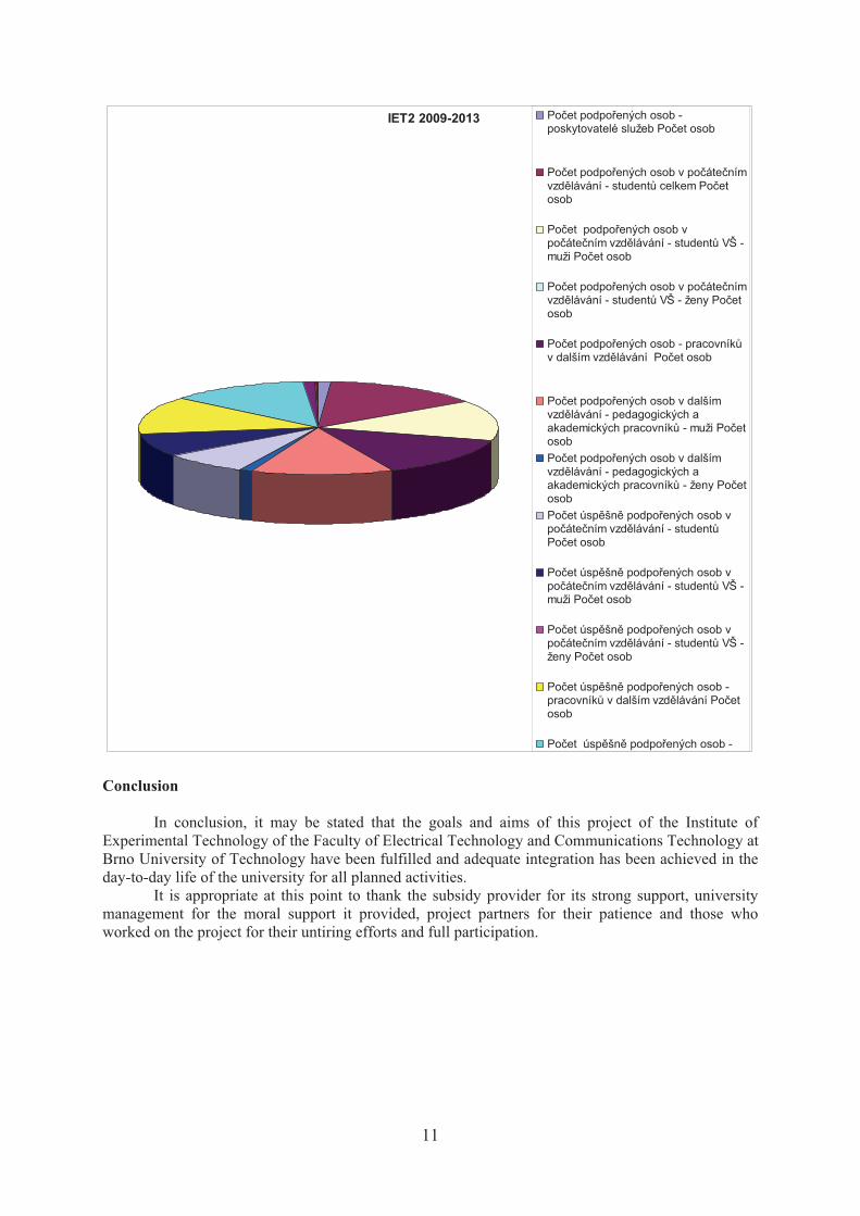
11
IET2 2009-2013 Po�et podpo�ených osob -poskytovatelé služeb Po�et osob
Po�et podpo�ených osob v po�áte�nímvzd�lávání - student� celkem Po�etosob
Po�et podpo�ených osob vpo�áte�ním vzd�lávání - student� VŠ -muži Po�et osob
Po�et podpo�ených osob v po�áte�nímvzd�lávání - student� VŠ - ženy Po�etosob
Po�et podpo�ených osob - pracovník�v dalším vzd�lávání Po�et osob
Po�et podpo�ených osob v dalšímvzd�lávání - pedagogických aakademických pracovník� - muži Po�etosobPo�et podpo�ených osob v dalšímvzd�lávání - pedagogických aakademických pracovník� - ženy Po�etosobPo�et úsp�šn� podpo�ených osob vpo�áte�ním vzd�lávání - student�Po�et osob
Po�et úsp�šn� podpo�ených osob vpo�áte�ním vzd�lávání - student� VŠ -muži Po�et osob
Po�et úsp�šn� podpo�ených osob vpo�áte�ním vzd�lávání - student� VŠ -ženy Po�et osob
Po�et úsp�šn� podpo�ených osob -pracovník� v dalším vzd�lávání Po�etosob
Po�et úsp�šn� podpo�ených osob - Conclusion In conclusion, it may be stated that the goals and aims of this project of the Institute of Experimental Technology of the Faculty of Electrical Technology and Communications Technology at Brno University of Technology have been fulfilled and adequate integration has been achieved in the day-to-day life of the university for all planned activities. It is appropriate at this point to thank the subsidy provider for its strong support, university management for the moral support it provided, project partners for their patience and those who worked on the project for their untiring efforts and full participation.
12
Faculty of Electrical Engineering and Communication Prof. Jarmila D�dková The Faculty of Electrical Engineering and Communications Technology is the third-largest faculty at Brno University of Technology and one of the leading electrical engineering faculties in the CR. The faculty boasts a rich history as the first electrical engineering disciplines were already being taught at BUT Brno in 1905. Since 1959, when an independent Energy Faculty was founded and later transformed into the Faculty of Electrical Engineering, almost 25,000 students have successfully graduated from the faculty's engineering program. The faculty acquired its current name in 2001: the Faculty of Electrical Engineering and Communications Technology (FEEC). During the more than 50 years of its existence, the individual faculty sites were distributed throughout Brno, in locations ranging from the Bozetechova Cloister to the current building of the VUT rectorate on Antoninska Street, Purkyn Street and, not long ago, the Dean's headquarters on Udolni Street. A large portion of the faculty may also be found in the Kolejni student complex.
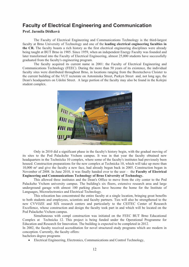
Only in 2010 did a significant phase in the faculty's history begin, with the gradual moving of its sites to the Pod Palackeho Vrchem campus. It was in that year the faculty obtained new headquarters in the Techniicka 10 complex, where some of the faculty's institutes had previously been housed. Construction preparations for the new complex at Technicka 10, which will take up more than 10,000 m² and give the faculty a new face, had already begun back in 2005. Construction began in November of 2008. In June 2010, it was finally handed over to the user – the Faculty of Electrical Engineering and Communications Technology of Brno University of Technology. This allowed three institutes and the Dean's Office to move from the city center to the Pod Palackeho Vrchem university campus. The building's six floors, extensive research area and large underground garage with almost 100 parking places have become the home for the Institute of Languages, Microelectronics and Electrical Technology. This relocation has concentrated the entire faculty at a single location, bringing great benefits to both students and employees, scientists and faculty partners. Ties will also be strengthened to the new CVVOZE and SIX research centers and particularly to the CEITEC Center of Research Excellence, whose construction and design the faculty took part in and which will be located on the Pod Palackeho Vrchem campus. Simultaneous with compl construction was initiated on the FEEC BUT Brno Educational Complex at Technicka 12. This project is being funded under the Operational Programme for Education and Research for Innovation. The building is expected to be completed in 2012. In 2002, the faculty received accreditation for novel structured study programs which are modern in conception. Currently, the faculty offers: bachelors degree programs
� Electrical Engineering, Electronics, Communications and Control Technology,

13
� Biomedical Engineering and Bioinformatics, two-year masters programs (postgraduate)
� Electrical Engineering, Electronics, Communications and Control Technology, � Biomedical Engineering and Bioinformatics,
doctoral programs � Electrical Engineering and Communications Technology.
Currently more than 4200 students study at the faculty in all forms of state-supported study. The style of study is completely compatible with instructional systems in use in the European Union, thus enabling full mobility for FEEC BUT students in the European study and research area. Approximately 230 academics are engaged in educational and research activity (professors, associate professors, lecturers, assistants, instructors, pedagogical staff and research personnel), along with approximately 200 other support staff. The faculty's programs of study are oriented toward a broad spectrum of research areas: control technology and robotics, biomedical engineering, bioinformatics, our electrical and electronic engineering, electronics and electrical technology, microelectronics, radio electronics and teleinformatics. It would be difficult to find an industry or important firm, research institution or state institution that did not have our graduates on staff. A number of our graduates may be found abroad and in high governmental and political functions in our country. Graduates of the faculty nevertheless continue to be in short supply, particularly recently with the growing interest of electrical engineering firms in collaboration and in sharp, skillful holders of bachelors and engineering degrees in electrical engineering. All of the faculty's educational and research activity must be funded. Funding sources include contributions and targeted subsidies from the Ministry of Education. These sources, unfortunately, have been reduced by 25% over the past two years. To a significant extent, instructors and researchers in the faculty's research and development program have made up for these sources by their own activities above and beyond the call of duty. A large share of the credit for maintaining material and financial resources must also go to researchers working on projects funded by grants from the Czech Science Foundation, the Grant Agency of the Academy of Sciences of the Czech Republic, the Ministry of Industry and Trade of the Czech Republic, the European Commission in FP6 and FP7 and the University Development Fund, along with all employees who worked with lead researchers in the faculty's four projects and its three research centers.

14
Eaton Elektrotechnika Ltd. Ing. Petr Slavata Eaton Elektrotechnika Ltd. Eaton Elektrotechnika Ltd. Komárovská 2406, 193 00 Praha 9 T�ebovská 480, 562 03 Ústí nad Orlicí tel.: +420 267 990 440 tel.: +420 465 519 611
Technical support: tel.: +420 267 990 440, e-mail: [email protected]
Eaton is above all associated with Moeller brand circuit breakers and residual current devices in the awareness of the professional public. However, Eaton is nowadays active as a producer and distributor of a wide range of electrical products and supplier of comprehensive solutions in the field of power supply quality. Eaton is an important employer in the Czech Republic with more than 1,500 employees here in various professions. Development is a never-ending process Eaton Elektrotechnika (formerly Moeller Elektrotechnika) entered onto the Czech market in 1993 as part of the Felten & Guilleaume Group. In 1998, the company commenced integration into the Moeller Group, dealing in production of devices for household and industrial installation and devices for distribution of electricity. Ten years later, the Moeller Group was bought by the Eaton Corporation, an international group. The company’s eighteen years of activity on the Czech market can be summed up in this manner.
For a company to be successful, it must open itself to changes and react flexibly to the requirements of its customers. Eaton’s product portfolio includes devices for household and industrial electrical installation and devices for distribution of electricity. Eaton is also active as a supplier of comprehensive solutions in the field of power supply quality. The company nowadays provides comprehensive solutions for projects consisting in deliveries of components and sets of components, above all HV and UPS.
Prague Office Ústí nad Orlicí Office

15
Eaton in the Czech Republic Eaton Elektrotechnika has two offices in the Czech Republic (in Prague and in Ústí nad Orlicí), which provide commercial and technical support to customers, not only in the Czech Republic, but also in selected countries of the former Soviet Union (Kazakhstan, Azerbaijan, Georgia, Belarus,…) and the former Yugoslavia (Slovenia, Croatia, Montenegro,…). The production plant in Suchdol nad Lužnicí is an important part of Eaton Elektrotechnika. It is especially switchgear cabinets and switchboards, residual current devices, circuit breakers and other components that are produced here. With almost a thousand workers, the plant is one of the most important employers in the South Bohemian Region. The BDC distribution and warehouse centre in Poho�elice near Brno also plays an important role in terms of the group, ensuring deliveries of the whole range of Eaton and Moeller products to customers, not only in the Czech Republic, but also in countries of Central and Eastern Europe. Other than Eaton Elektrotechnika, Eaton Industries is also active in the Czech Republic, dealing in production and sale of automotive components. Hydraulic systems for the automobile industry are produced in Chomutov, above all liquid distribution lines for air-conditioning, power steering systems and brakes. Eaton Corporation celebrating 100 years of business The international group, the Eaton Corporation, is this year celebrating 100 years since its foundation. Eaton’s roots reach right back to 1911, when J. O. Eaton started to do business with his partners in the American town of Bloomfield. The company bears his name to this very day. Their small company initially produced only gearboxes and axles for lorries. Over the 100 years of its existence, Eaton has managed to establish several divisions that operate all over the world. The Eaton Corporation is nowadays active in the field of electrical systems, equipment for distribution and management of electricity; hydraulic components, systems and services for industrial and mobile equipment; fuel, hydraulic and pneumatic systems in the aviation industry for civil and military use; drive train systems and units for freight and passenger vehicles ensuring optimisation of performance, fuel consumption and safety. The Eaton Corporation currently employs approximately 70,000 people the world over and supplies its products to customers in more than 150 countries. The turnover of the Eaton Corporation Group as a whole reached the level of USD 11.9 billion in 2009.
16
SVS FEM sro Tibor Bachorec, PhD The objective of the Institute of Experimental Technology 2 project is to prepare highly qualified specialists for the needs of industry. The real world expects that they will have the ability to formulate and solve technical problems for which computer simulation is essential. Teaching computer simulation in keeping with real-world demands develops students' ability to:
� Define a technical problem � Create a numerical model � Undertake calculations � Evaluate and verify results � Propose and verify solutions � Carry out optimization and sensitivity
analysis
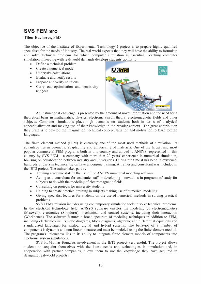
An instructional challenge is presented by the amount of novel information and the need for a theoretical basis in mathematics, physics, electronic circuit theory, electromagnetic fields and other subjects. Computer simulations place high demands on students both in terms of analytical conceptualization and making use of their knowledge in the broader context. The great contribution they bring is to develop the imagination, technical conceptualization and motivation to learn foreign languages. The finite element method (FEM) is currently one of the most used methods of simulation. Its advantage lies in geometric adaptability and universality of materials. One of the largest and most popular commercial FEM programs both in this country and abroad is ANSYS, represented in this country by SVS FEM – a company with more than 20 years' experience in numerical simulation, focusing on collaboration between industry and universities. During the time it has been in existence, hundreds of users in technical fields have undergone training. A trainer and consultant was included in the IET2 project. The trainer takes part by:
� Training academic staff in the use of the ANSYS numerical modeling software � Acting as a consultant for academic staff in developing innovations in programs of study for
subjects to do with the modeling of electromagnetic fields � Consulting on projects for university students � Helping to create practical training in subjects making use of numerical modeling � Giving specialist lectures for students on the use of numerical methods in solving practical
problems SVS FEM's mission includes using contemporary simulation tools to solve technical problems. In the electrical technology field, ANSYS software enables the modeling of electromagnetics (Maxwell), electronics (Simplorer), mechanical and control systems, including their interaction (Workbench). The software features a broad spectrum of modeling techniques in addition to FEM, including electronic circuits, state diagrams, block diagrams, algebraic and differential equations and standardized languages for analog, digital and hybrid systems. The behavior of a number of components is dynamic and non-linear in nature and must be modeled using the finite element method. The program's uniqueness lies in its ability to integrate finite element models of components into electronic system simulations. SVS FEM's has found its involvement in the IET2 project very useful. The project allows students to acquaint themselves with the latest trends and technologies in simulation and, in cooperation with partner companies, allows them to use the knowledge they have acquired in designing real-world projects.

17
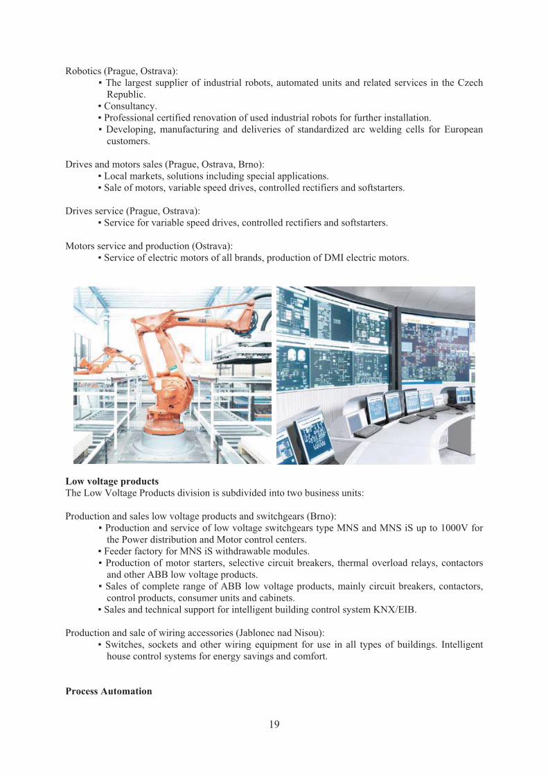
ABB in the Czech Republic Leader in power and automation
ABB is a global leader in power and automation, providing complex services to industrial companies and to power producers and distributors. ABB’s state-of-the-art technologies enable its customers to improve performance while lowering the environmental impact of their activities. ABB’s products and services have been present in the Czech Republic since 1970 and the first ABB company in the Czech Republic was formally set up in 1991. During the 1990s, the ABB group grew by taking up new companies to form the current ABB Ltd. (a limited-liability company).
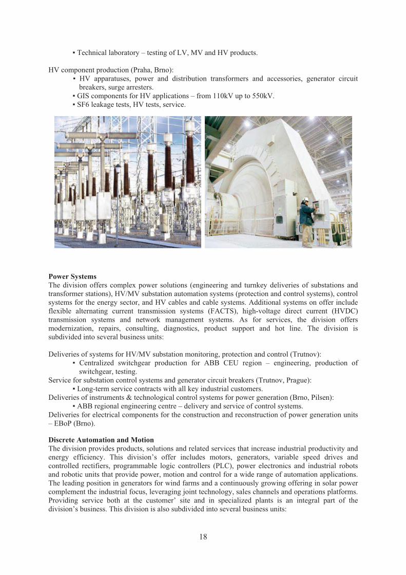
The ABB group was established in 1988 by a merger of Swedish company Asea with Swiss company BBC Brown Boveri. Asea’s history dates back to 1883, while BBC Brown Boveri was founded in 1891. The company is based in Zurich, Switzerland. ABB has operations in more than 100 countries of the world and has about 120,000 employees. ABB currently consists of five divisions: Power Products, Power Systems, Discrete Automation and Motion, Low Voltage Products and Process Automation. Power Products Power Products are the key products to transmit and distribute electricity. The division mainly produces and delivers HV substations and apparatuses, MV substations, switchgears and apparatuses, protection for power generation and industry, instrument transformers and sensors, power and distribution transformers. As for services, the division offers modernization, repairs, consulting, diagnostics, product support and hot line. The PP division is subdivided into several business units: MV production and sales (Brno):
� Production of MV switchgears, instrument transformers and sensors. � RFFF for air-insulated switchgears. � GFFF for instrument transformers and sensors. � Technology Centre–research & development in the field of instrument transformers, sensors
and air-insulated switchgears. � Service for MV products.
18
� Technical laboratory – testing of LV, MV and HV products. HV component production (Praha, Brno):
� HV apparatuses, power and distribution transformers and accessories, generator circuit breakers, surge arresters.
� GIS components for HV applications – from 110kV up to 550kV. � SF6 leakage tests, HV tests, service.
Power Systems The division offers complex power solutions (engineering and turnkey deliveries of substations and transformer stations), HV/MV substation automation systems (protection and control systems), control systems for the energy sector, and HV cables and cable systems. Additional systems on offer include flexible alternating current transmission systems (FACTS), high-voltage direct current (HVDC) transmission systems and network management systems. As for services, the division offers modernization, repairs, consulting, diagnostics, product support and hot line. The division is subdivided into several business units: Deliveries of systems for HV/MV substation monitoring, protection and control (Trutnov):
� Centralized switchgear production for ABB CEU region – engineering, production of switchgear, testing.
Service for substation control systems and generator circuit breakers (Trutnov, Prague): � Long-term service contracts with all key industrial customers.
Deliveries of instruments & technological control systems for power generation (Brno, Pilsen): � ABB regional engineering centre – delivery and service of control systems.
Deliveries for electrical components for the construction and reconstruction of power generation units – EBoP (Brno). Discrete Automation and Motion The division provides products, solutions and related services that increase industrial productivity and energy efficiency. This division’s offer includes motors, generators, variable speed drives and controlled rectifiers, programmable logic controllers (PLC), power electronics and industrial robots and robotic units that provide power, motion and control for a wide range of automation applications. The leading position in generators for wind farms and a continuously growing offering in solar power complement the industrial focus, leveraging joint technology, sales channels and operations platforms. Providing service both at the customer’ site and in specialized plants is an integral part of the division’s business. This division is also subdivided into several business units:
19
Robotics (Prague, Ostrava): � The largest supplier of industrial robots, automated units and related services in the Czech
Republic. � Consultancy. � Professional certified renovation of used industrial robots for further installation. � Developing, manufacturing and deliveries of standardized arc welding cells for European
customers. Drives and motors sales (Prague, Ostrava, Brno):
� Local markets, solutions including special applications. � Sale of motors, variable speed drives, controlled rectifiers and softstarters.
Drives service (Prague, Ostrava):
� Service for variable speed drives, controlled rectifiers and softstarters.
Motors service and production (Ostrava): � Service of electric motors of all brands, production of DMI electric motors.
Low voltage products The Low Voltage Products division is subdivided into two business units: Production and sales low voltage products and switchgears (Brno):
� Production and service of low voltage switchgears type MNS and MNS iS up to 1000V for the Power distribution and Motor control centers.
� Feeder factory for MNS iS withdrawable modules. � Production of motor starters, selective circuit breakers, thermal overload relays, contactors
and other ABB low voltage products. � Sales of complete range of ABB low voltage products, mainly circuit breakers, contactors,
control products, consumer units and cabinets. � Sales and technical support for intelligent building control system KNX/EIB.
Production and sale of wiring accessories (Jablonec nad Nisou):
� Switches, sockets and other wiring equipment for use in all types of buildings. Intelligent house control systems for energy savings and comfort.
Process Automation

20
The Process Automation division provides customers with best solutions for plant control and optimization, as well as industry-specific application knowledge. The industries served include particularly metals and minerals, pulp and paper, power, chemicals and pharmaceuticals, oil and gas, marine and the production of turbochargers. Key customer benefits include improved asset productivity and energy savings. This division is subdivided into several business units: Process automation for the local market (Prague, Ostrava, Most, Brno):
� Deliveries of control systems and drive applications, deliveries of complex automation solutions for technological processes and control systems service.
� Control systems engineering, instrumentation & analytics, drives engineering and service for instrumentation & analytics.
� Sales of control systems and industrial instrumentation & analytics. Operation Center Czech Republic (Ostrava):
� Global engineering center for process automation in industries such as metals and minerals, marine, oil, gas and petrochemical, pulp and paper and other industries.
� Project design, engineering and commissioning of control systems and drives. Our achievements ABB Czech Republic among suppliers to the world’s tallest building One of the most closely watched constructions today is undoubtedly the Khalifa Tower (Burj Khalifa). The skyscraper in the most populous city of the United Arab Emirates has 162 floors and towers more 828 meters above ground. One of the suppliers to this unique construction is ABB Czech Republic – PPMV Brno, which has delivered a total of 48 pieces of airinsulated medium voltage switchgears over the past 2 years of construction works. The deliveries ensure the supply of vital electric power to the building (for air-conditioning, lighting, communication equipment, etc.) and to the adjacent complex of lakes with fountains, which girdle the tower and add to its luxurious environment. ABB helps create a giant lake in the old Most area Several decades ago, the area under the now non-existent old city of Most was extracted as a brown coal mine. Only the well-know Gothic church was transported and survived. A huge pit occurred, as many as 70 meters deep. After years of thought on how to secure the pressures of the surrounding rock, a decision was taken to flood the whole area. Water would stabilize slopes and create conditions for building a recreational area larger than Mácha’s lake. Since there is not enough water for flooding on the site, the existing industrial water piping is used to pump water from the Oh�e river 24km away. Near the Stranná community, Povodí Oh�e (Oh�e Basin Management) operates a pump station equipped with 3 ABB’s ACS 1000 MV variable speed drives. The new lake started to fill with water in October 2008 and should be full until the end of 2011. The water flows through 1,200mm-diameter piping into distributive shaft in Komo�any and then through 800mm piping to Most. The average rate of flow is 600–800 l/s, with maximum reaching 1,200 l/s. After filling up, the lake will contain 69 million cubic meters of water, with an area of 311 hectares. The information stated above suggests that this is a grandiose project involving immense volume of transported water. One of its highlights is the reliability of the equipment and the considerable energy savings thanks to the efficient regulation of the pump performance using ABB’s variable speed drives. ABB robots help to automate Hamé’s logistic centre Robotics division completed the project of automated depalletizing, packaging and palletizing of glasses in Hamé’s new Central Distribution Stock in Staré M�sto. The goal was to fully automate the process, improving its productivity. Our solution is based on three ABB IRB660 industrial robots with grippers and the necessary peripherals, enabling manipulation with dozens of various types of packaging. The palletizing process is controlled by PickMasterTM5 software, allowing customers easy and independent programming of new products in the future. From the beginning to the end, when the products are wrapped and stacked on the pallet, no glass is touched by the human hand and the line handles more than 4 glasses per second. The resulting efficiency of the system is very high and brings Hamé the required growth in productivity of its operations.

21
ABB s.r.o. successfully implements large amount of projects and deliveries in the Czech Republic ABB has become the supplier of medium voltage switchgear retrofits for all units of Dukovany nuclear power station and for the first unit of Temelín nuclear power station. Retrofitting, i.e. the replacement of an original switch with a new one, increases the reliability of switchgear, at the same time reducing maintenance requirements. Medium voltage equipment and switchgear have been used in a number of major projects, such as TPSA Kolín automobile factory, O2 Arena in Prague or in Zli�ín shopping centre. We are no. 1 supplier of wiring accessories in the Czech market. ABB switches and sockets are present in an endless number of housing units, in office and industrial buildings, as well as at such exclusive places as the representation halls of the Prague Castle or the Centre of Air Navigation Services at Jene� near Prague. Motors regulated by ABB’s variable speed drives have been supplied to a number of branches of Czech industry, particularly to heat generation and power. The results of energy savings calculations and the return on investment have been proved in practice. In the field of robotics, we have successfully delivered complete automated palletizing lines for rubber briquettes to Synthos Kralupy a. s. and several robotized units for CNS machining centers to Kovokon Kunovice s. r. o. ABB implemented an extension of the ethylene unit control system for the new extractive benzene distillation operation for Unipetrol RPA, s. r. o. The project was implemented during full operation, without any need for technology shutdown. Among other things, ABB supplied and installed a new modern controller and special I/O units for use in explosive environment. The new unit is controlled from the central control room of the ethylene unit and can be controlled from the existing operator station as well as from a new operator station with ABB’s System 800xA system for MOD in place. ABB Ltd. Sokolovská 84-86 186 00 Praha 8 �eská republika Tel.: +420 234 322 111 Fax: +420 234 322 113 www.abb.cz
22
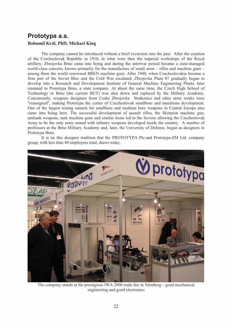
Prototypa a.s. Bohumil Král, PhD, Michael King The company cannot be introduced without a brief excursion into the past. After the creation of the Czechoslovak Republic in 1918, in what were then the imperial workshops of the Royal artillery, Zbrojovka Brno came into being and during the interwar period became a state-managed world-class concern, known primarily for the manufacture of small arms – rifles and machine guns – among them the world renowned BREN machine gun). After 1948, when Czechoslovakia became a firm part of the Soviet Bloc and the Cold War escalated, Zbrojovka Plant 07 gradually began to develop into a Research and Development Institute of General Machine Engineering Plants, later renamed to Prototypa Brno, a state company. At about the same time, the Czech High School of Technology in Brno (the current BUT) was shut down and replaced by the Military Academy. Concurrently, weapons designers from Ceska Zbrojovka Strakonice and other arms works were "reassigned", making Prototypa the center of Czechoslovak smallbore and munitions development. One of the largest testing tunnels for smallbore and medium bore weapons in Central Europe also came into being here. The successful development of assault rifles, the Skorpion machine gun, antitank weapons, tank machine guns and similar items led to the Soviets allowing the Czechoslovak Army to be the only army armed with infantry weapons developed inside the country. A number of professors at the Brno Military Academy and, later, the University of Defense, began as designers in Prototypa Brno. It is on this designer tradition that the PROTOTYPA Plc.and Prototypa-ZM Ltd. company group, with less than 40 employees total, draws today.
The company stands at the prestigious IWA 2006 trade fair in Nürnberg – good mechanical
engineering and good electronics

23
After the "Velvet Revolution" of 1989 and the subsequent conversion of industrial and the military, particularly as involves privatization, both companies focused primarily on munitions and weapons testing for the government, as well as forensic and military purposes. The companies have been able to ride the wave of electronic technology moving into the field and thus have augmented the tradition of Brno designers by gradually becoming suppliers of quality electronic testing systems around the globe. There is a long designer tradition today at both companies bearing the PROTOTYPA name, but the Institute of Theoretical and Experimental Electrical Engineering, in charge of the IET2 project, suffered a discontinuity of several years' duration when the shutdown of BUT and its replacement by the Military Academy in 1951-1959 violently interrupted the Institute's natural development. Ales Blaha, then head of the Institute, left for Bratislava in 1952 and his time-tested project management techniques and selection of capable talent basically came to an end. His students in the newly created institutes like the Institute of Scientific Instruments of the Academy of Sciences and the Institute of Energy Brno, however, have carried Blaha's style with them into the successor companies. The current Institute of Theoretical and Experimental Electrical Engineering, in its IET2 project, is attempting to reinvigorate Blaha's ideas about educating electrical engineers. PROTOTYPA management has welcomed the IET project for three logical reasons. The first reason has to do with personnel. PROTOTYPA's representative has 20 years' experience (1963-1983) at the reopened Department of Theoretical and Experimental Electrical Engineering in the development and instructional areas and cares deeply about development. The second reason has to do with moving. PROTOTYPA's headquarters are in close proximity to UTEE, a significant advantage for collaboration purposes. The third, decisive reason is mutual understanding that without ties between instruction, development and industrial implementation of new designs, both universities and the industry are doomed to stagnation, with unending consequences for individual actors, groups and, significantly, the country as a whole. As has been emphasized in the introduction, we are a small company, one which places somewhat different requirements on electrical engineering graduates than is normal within today's educational framework. A small company does not seek specialists. Instead it requires well-educated "universalists", with abilities anchored in fundamental physics, mathematics and "general" electrical engineering. The "superstructure" – knowledge of programming, computer technology, graphics, measurement technology, etc. – are now taken for granted in all disciplines and do not constitute a competitive advantage. There is a noticeable absence today in electrical engineering of knowledge of the "fundamentals", especially in smaller companies which develop and produce on a "one-off" basis, continually modifying their designs based upon customer demand and functioning at the borders of several disciplines. Let me generalize the point, without worrying too much about precision. Why were Professor Blaha and his students so successful? Is there anything we can learn from the past? I'm not sure – maybe... The young Blaha went to grammar school in France. It was logical, then, that as an engineer and professor, he would make use of his experience in the French schools and his knowledge of French science and industry. Indeed, the entire First Republic was tied to France to a significant extent. Prime evidence of this is the French capital invested in prewar Skoda Pilsen. We were surprised to read his article in Electrical Engineering Horizons entitled Electrical Engineering and Mathematics from 1934 (Blaha was 28 years old and shortly thereafter became a "fresh" associate professor). [1] We concur with his opinion that the educational system, particularly in a small country, should foresee the "demands of the time" and produce a certain number of engineers educated in general electrical engineering, capable of carrying out tasks which are new to them and for which they have not been explicitly "trained". Army generals are sometimes put down by noting they always prepare for the war which has already passed, rather than imagining how the next will be. Hopefully Czech electrical engineers can avoid this fate in the future. Projects like IET2, CEITEC and others may help them to do so. It's also necessary, of course, to present models of successful electrical engineers in recent history to young people, to make them aware that, aside from the football players, tennis players,

24
singers and TV stars, there also exist unknown heroes of science who are worthy of admiration. People who often make the decisions about the country's technological and economic base and the level of education in the electrical engineering field. People on whose shoulders we continue to stand, even if we often do so unawares and unsystematically. What kind of work might students, graduates, doctoral graduates and lecturers encounter at PROTOTYPA? For the most part, events of a one-off nature. Every shot and every explosion (turning off power to an amplifier, electrical shorts, industrial accidents, etc.) is a one-off affair which must be captured, measured, analyzed and documented. Measurements of speeds up to several thousand meters per second are taken, pressures of several hundred MPa are measured with increases on the order of tens of microseconds, dynamic measurement is done on the axis of entry, recoil is measured, impact energy, cadence, etc. Then there are small-scale automation measurement tasks emphasizing safety, heat chamber experiments with temperatures ranging from –60 to +60º C, measurements in dust and a rain chambers, the testing of ballistic materials (vests, helmets, vehicle armor, etc.) Something new is that students may now come into contact with the NQR radio-frequency method (nuclear quadrupole resonance), used around the world to identify explosives, medications and drugs. [4] Testing in this area, which is a focus of PROTOTYPA, a.s., and Prototypa-ZM, s.r.o, concerns more than just weapons and ammunition. The state emergency system, national defense and security all have their specific characteristics and find testing facilities such as those of PROTOTYPA essential. In such a company, the electrical engineer must have knowledge at his or her disposal line at the boundary of several disciplines and must be capable of flexibly reacting to demands which may come in from essentially the entire world. Virtually every piece of experimental equipment ordered differs from the last such piece to fulfill customer demands. The electrical engineer in a small company thus requires broad theoretical and practical background and must always seek to improve! The electrical engineer in a small company will certainly never be bored! A line from Blaha: "Are you doing something useful here or just playing around?" That observation holds absolutely in our environment! [2] [1] Blaha, A.: Elektrotechnik a Matematika [The Electrical Engineer and Mathematics] [2] Dadok, J: Moje Vzpominky na Profesora Alese Blahu [My Memories of Professor Ales Blaha]. Article manuscript, May 2011 [3] www.prototypa.cz [4] Anderle, M.: Jak Vy�enichat Výbušninu? [How are Explosives Sniffed Out?] 21st Century Monthly. Revue Objev�, V�dy, Techniky a Lidí [Review of Inventions, Science, Technology and People], No.9 (2011), pp.10-12.
25
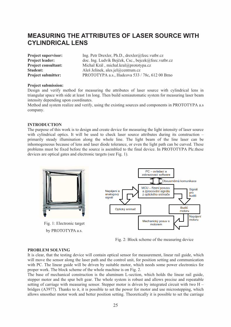
MEASURING THE ATTRIBUTES OF LASER SOURCE WITH CYLINDRICAL LENS Project supervisor: Ing. Petr Drexler, Ph.D., [email protected] Project leader: doc. Ing. Ludvík Bej�ek, Csc., [email protected] Project consultant: Michal Král , [email protected] Student: Aleš Jelínek, [email protected] Project submitter: PROTOTYPA a.s., Hudcova 533 / 78c, 612 00 Brno Project submission: Design and verify method for measuring the attributes of laser source with cylindrical lens in triangular space with side at least 1m long. Then build semiautomatic system for measuring laser beam intensity depending upon coordinates. Method and system realize and verify, using the existing sources and components in PROTOTYPA a.s company. INTRODUCTION The purpose of this work is to design and create device for measuring the light intensity of laser source with cylindrical optics. It will be used to check laser source attributes during its construction – primarily steady illumination along the whole line. The light beam of the line laser can be inhomogeneous because of lens and laser diode tolerance, or even the light path can be curved. These problems must be fixed before the source is asembled to the final device. In PROTOTYPA Plc.these devices are optical gates and electronic targets (see Fig. 1).
Fig. 1: Electronic target
by PROTOTYPA a.s.
Fig. 2: Block scheme of the measuring device
PROBLEM SOLVING It is clear, that the testing device will contain optical sensor for measurement, linear rail guide, which will move the sensor along the laser path and the control unit, for position setting and communication with PC. The linear guide will be driven by suitable motor, which needs some power electronics for proper work. The block scheme of the whole machine is on Fig. 2. The base of mechanical construction is the aluminum L-section, which holds the linear rail guide, stepper motor and the spur belt gear. The whole system is robust and allows precise and repeatable setting of carriage with measuring sensor. Stepper motor is driven by integrated circuit with two H – bridges (A3977). Thanks to it, it is possible to set the power for motor and use microstepping, which allows smoother motor work and better position setting. Theoretically it is possible to set the carriage
26
position with resolution 0,0625 mm, but the true accuracy is little bit worse, mainly due to spur belt elasticity. As the optical sensor a photodiode was selected. The main attributes are active angle and the wave length sensitivity. Photodiode signal is amplified in differential amplifier and it is measured by AD converter of the microcontroller. Photodiode is connected to the main board by the shielded cable, to minimize the electromagnetic noise. Control of the device and communication with PC is solved by microcontroller by Atmel company (Atmega 168). For communication, there is serial link RS-232. PC software is able to send commands to set device attributes, or to start some action. It is possible to change scan speed and quantity of samples. The other commands are used to initialize the machine and start the scanning sequence. Data, sent from device to the computer, are only the measured values, nothing else is implemented in this direction. Communication protocol corresponds to this fact – from PC to device flow data in pairs command + parameter, to the contrary it is always block of data of the known size.
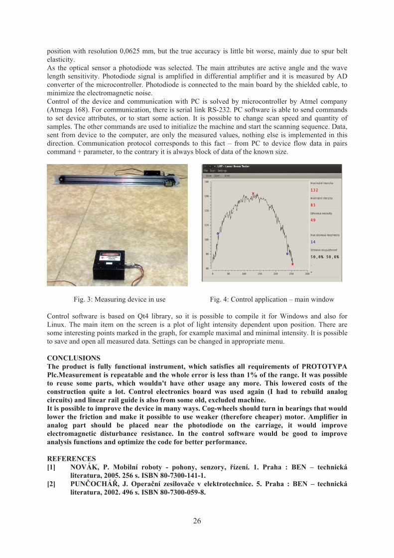
Fig. 3: Measuring device in use
Fig. 4: Control application – main window Control software is based on Qt4 library, so it is possible to compile it for Windows and also for Linux. The main item on the screen is a plot of light intensity dependent upon position. There are some interesting points marked in the graph, for example maximal and minimal intensity. It is possible to save and open all measured data. Settings can be changed in appropriate menu. CONCLUSIONS The product is fully functional instrument, which satisfies all requirements of PROTOTYPA Plc.Measurement is repeatable and the whole error is less than 1% of the range. It was possible to reuse some parts, which wouldn't have other usage any more. This lowered costs of the construction quite a lot. Control electronics board was used again (I had to rebuild analog circuits) and linear rail guide is also from some old, excluded machine. It is possible to improve the device in many ways. Cog-wheels should turn in bearings that would lower the friction and make it possible to use weaker (therefore cheaper) motor. Amplifier in analog part should be placed near the photodiode on the carriage, it would improve electromagnetic disturbance resistance. In the control software would be good to improve analysis functions and optimize the code for better performance. REFERENCES [1] NOVÁK, P. Mobilní roboty - pohony, senzory, �ízení. 1. Praha : BEN – technická
literatura, 2005. 256 s. ISBN 80-7300-141-1. [2] PUN�OCHÁ�, J. Opera�ní zesilova�e v elektrotechnice. 5. Praha : BEN – technická
literatura, 2002. 496 s. ISBN 80-7300-059-8.

27
[3] KOENIG, A; MOO, B. E. Rozumíme C++. 1. Praha : Computer Press, 2003. 388 s. ISBN 80-7226-656-X.
[4] FUKÁTKO, T. Detekce a m��ení r�zných druh� zá�ení . 1. Praha : BEN – technická literatura, 2007. 192 s. ISBN 80-7300-193-3.
[5] QUIS, P. CNC shop [online]. 2010 [cit. 2010-11-29]. Produkty. Dostupné z WWW: <http://www.cncshop.cz/>.
[6] Nokia. Qt4 dokumentace [online]. 2011 [cit. 2011-05-24]. Dostupné z WWW: <http://qt.nokia.com/>.
28
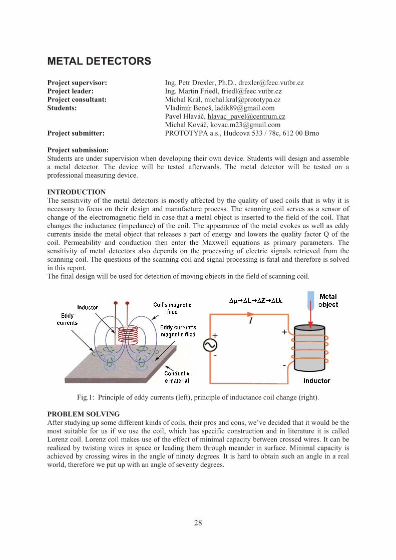
METAL DETECTORS Project supervisor: Ing. Petr Drexler, Ph.D., [email protected] Project leader: Ing. Martin Friedl, [email protected] Project consultant: Michal Král, [email protected] Students: Vladimír Beneš, [email protected] Pavel Hlavá�, [email protected] Michal Ková�, [email protected] Project submitter: PROTOTYPA a.s., Hudcova 533 / 78c, 612 00 Brno Project submission: Students are under supervision when developing their own device. Students will design and assemble a metal detector. The device will be tested afterwards. The metal detector will be tested on a professional measuring device. INTRODUCTION The sensitivity of the metal detectors is mostly affected by the quality of used coils that is why it is necessary to focus on their design and manufacture process. The scanning coil serves as a sensor of change of the electromagnetic field in case that a metal object is inserted to the field of the coil. That changes the inductance (impedance) of the coil. The appearance of the metal evokes as well as eddy currents inside the metal object that releases a part of energy and lowers the quality factor Q of the coil. Permeability and conduction then enter the Maxwell equations as primary parameters. The sensitivity of metal detectors also depends on the processing of electric signals retrieved from the scanning coil. The questions of the scanning coil and signal processing is fatal and therefore is solved in this report. The final design will be used for detection of moving objects in the field of scanning coil.
Fig.1: Principle of eddy currents (left), principle of inductance coil change (right). PROBLEM SOLVING After studying up some different kinds of coils, their pros and cons, we’ve decided that it would be the most suitable for us if we use the coil, which has specific construction and in literature it is called Lorenz coil. Lorenz coil makes use of the effect of minimal capacity between crossed wires. It can be realized by twisting wires in space or leading them through meander in surface. Minimal capacity is achieved by crossing wires in the angle of ninety degrees. It is hard to obtain such an angle in a real world, therefore we put up with an angle of seventy degrees.
29
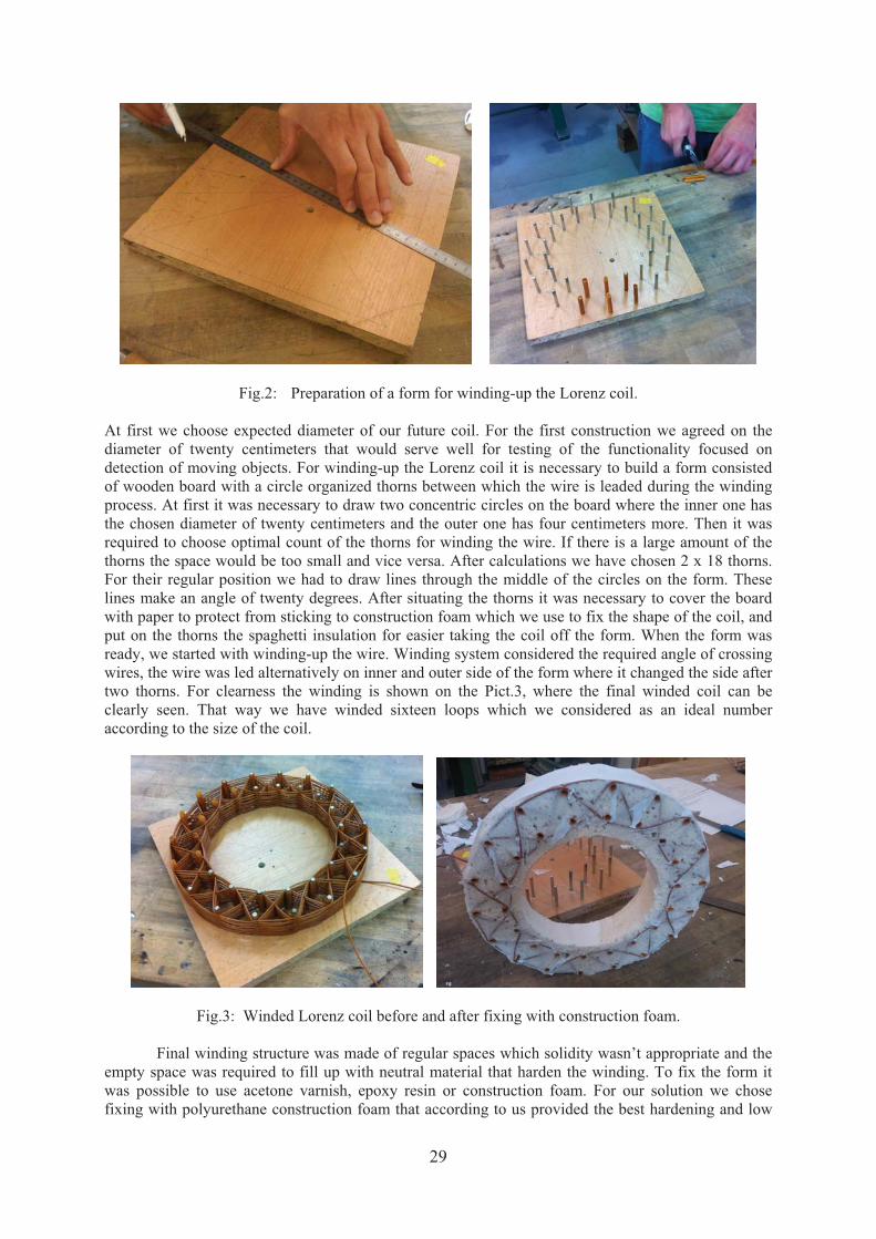
Fig.2: Preparation of a form for winding-up the Lorenz coil. At first we choose expected diameter of our future coil. For the first construction we agreed on the diameter of twenty centimeters that would serve well for testing of the functionality focused on detection of moving objects. For winding-up the Lorenz coil it is necessary to build a form consisted of wooden board with a circle organized thorns between which the wire is leaded during the winding process. At first it was necessary to draw two concentric circles on the board where the inner one has the chosen diameter of twenty centimeters and the outer one has four centimeters more. Then it was required to choose optimal count of the thorns for winding the wire. If there is a large amount of the thorns the space would be too small and vice versa. After calculations we have chosen 2 x 18 thorns. For their regular position we had to draw lines through the middle of the circles on the form. These lines make an angle of twenty degrees. After situating the thorns it was necessary to cover the board with paper to protect from sticking to construction foam which we use to fix the shape of the coil, and put on the thorns the spaghetti insulation for easier taking the coil off the form. When the form was ready, we started with winding-up the wire. Winding system considered the required angle of crossing wires, the wire was led alternatively on inner and outer side of the form where it changed the side after two thorns. For clearness the winding is shown on the Pict.3, where the final winded coil can be clearly seen. That way we have winded sixteen loops which we considered as an ideal number according to the size of the coil.
Fig.3: Winded Lorenz coil before and after fixing with construction foam. Final winding structure was made of regular spaces which solidity wasn’t appropriate and the empty space was required to fill up with neutral material that harden the winding. To fix the form it was possible to use acetone varnish, epoxy resin or construction foam. For our solution we chose fixing with polyurethane construction foam that according to us provided the best hardening and low

30
weight of the coil. After curing it was necessary to cut the extra foam to desired shape. During the cutting process we had to make sure that we wouldn’t damage the wires of the coil. When the coil had the final shape we needed to get it out of the form. It was necessary to carefully separate the bottom of the coil from the form. With slow cutting we managed to do that without damaging any wires. Now the only thing that left us was final cutting of last imperfections and wrapping to transparent sticking tape and the coil was ready for testing of flying objects detection. CONCLUSIONS Until now we practically tested moving metal object detection with a classic winded coil. It was a winding with a small size therefore the peak that was measured by oscilloscope on this simple detector reached the value of 2V. After these tests we studied the questions of coils used in various metal detectors. We’ve chosen the Lorenz coil because of its small capacity between single wires and every loop. Nowadays we are in stage of testing measurements of this coil with aforementioned peak detector. In the near future we are about to take a closer look on developing of appropriate electrical evaluation networks. The testing coil is much bigger than the classic winded one used for first verifying of theory. That’s why it will be necessary to adapt electronics to the fact that the peaks measured on Lorenz coil with usage of the small metal objects will be several times smaller. REFERENCES [1] JARCHOVSKÝ, Zden�k; SOCHÁ�, Petr. Renesance Lorenzovy cívky pro detektory kov�.
Praktická elektronika. 2001, 9, s. 12-13. ISSN 1211-328X. [2] HÁJEK, Jan; JARCHOVSKÝ, Zden�k. Detektory kovu - návod na stavbu. 1. vyd. Praha :
BEN – technická literatura, 2010. 256 s. ISBN 978-80-7300-220-6.

31
ROBOTIC CHASSIS Project supervisor: Ing. Petr Drexler, Ph.D., [email protected] Project leader: Ing. Martin Friedl , [email protected] Project consultant: Michal Král , [email protected] Students: Jakub H�lka, [email protected] Jozef Humaj, [email protected] Project submitter: PROTOTYPA a.s., Hudcova 533 / 78c, 612 00 Brno Project submission: Acquaint with problems service ballistics gun barrel. Peruse current method solving automated loading system and possibly hazards for work with unexploded munitions. On base gained piece of knowledge suggest own circuit and technical solution manipulator for attendance munitions. Suggest system for safe remove fail munitions, which will cooperates system of manipulator. Specify requirements on safe stowage space for unexploded munitions on base data intended submitter. On base suggestion realize functional samples systems manipulators and verify them practically. INTRODUCTION Ours target was suggest system safe remove unexploded munitions. Practically it looks like, that the after unsuccessful firing waits definite time, accordance with type of munitions, and after that the pyrotechnist removes unexploded munitions, witch can be enough dangerous. Therefore get past fit, to this a life threatening work exercised some manipulator, in our case mobile robot with robotic arm. In our thesis we deal with only part with robotic chassis, problems robotic arm is subject of next work, since they are setting high requirements on accuracy and sensitivity movement robotic arms, it is not possible in terms one's project all these requirements from time reasons realize.
Obr.1: Sample of ballistic barrel. To ours arrangement was used commercial robotic chassis, because it very speeds up work and we can more target on electrical engineering. To this chassis was necessary suggest concrete control system, to run function basic hardware and optimise control software. Resulting product would had enable wireless drive control by operator, safely distinguish hurdles and enough quickly take away unexploded munitions to the safe distance. To basic detection hurdles they are used four reflex infra sensor GP2YA0A21, every is placed over one wheel, so to was easy decide, that the direction is able to robot ride. Output from sensor is analogue and size tension is proportional to distance hurdles. More detailed picture about placing hurdles in front robot can extract from ultrasonic sonar SRF05 that can be turn by the help of servo. PROBLEM SOLVING Base of control system is processor PIC16F877 that does service all peripheries. Further they are on control board placed buttons and LCD display for easier debug application. Communication with
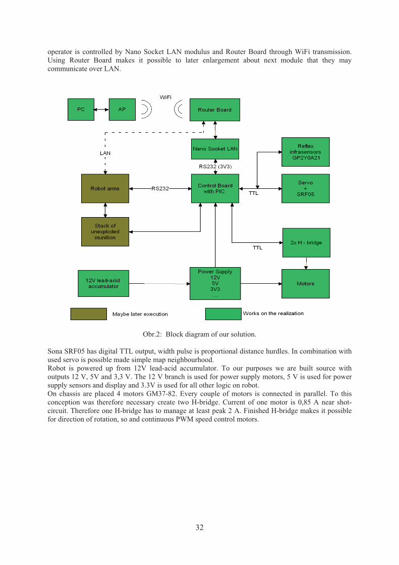
32
operator is controlled by Nano Socket LAN modulus and Router Board through WiFi transmission. Using Router Board makes it possible to later enlargement about next module that they may communicate over LAN.
Obr.2: Block diagram of our solution.
Sona SRF05 has digital TTL output, width pulse is proportional distance hurdles. In combination with used servo is possible made simple map neighbourhood. Robot is powered up from 12V lead-acid accumulator. To our purposes we are built source with outputs 12 V, 5V and 3,3 V. The 12 V branch is used for power supply motors, 5 V is used for power supply sensors and display and 3.3V is used for all other logic on robot. On chassis are placed 4 motors GM37-82. Every couple of motors is connected in parallel. To this conception was therefore necessary create two H-bridge. Current of one motor is 0,85 A near shot-circuit. Therefore one H-bridge has to manage at least peak 2 A. Finished H-bridge makes it possible for direction of rotation, so and continuous PWM speed control motors.

33
Obr.3: Sample robot and control board with sensors
CONCLUSIONS On base of submission we succeed suggest concrete solution of robot on safe transport unexploded munitions. We bought needed materials and step by step tested individual parts of the robot. At present finalize simple software for PC that makes it possible link up communication with Router Board on robot. The board power supply and H-bridge are also ready. To control board we begin create software for attendance of all periphery and communication with operator. We suppose that in September 2011 should be ready functional robot. REFERENCES [1] Novák, P. Mobilní roboty - pohony, senzory, �ízení. Praha : BEN – technická literatura,
2005. ISBN 80-7300-141-1 [2] Microchip PIC16F877 : Data Sheet [online]. Dostupné z: <http://ww1.microchip.com/downloads/en/DeviceDoc/30292c.pdf> [3] ConnectOne Nano SocketLAN : Data Sheet [online]. Dostupné z: <http://www.spezial.cz/pdf/Nano_Socket_LAN_DS.pdf> [4] SRF05 - Ultra-Sonic Ranger : Technical Specification [online]. Dostupné z: <http://www.robot-electronics.co.uk/htm/srf05tech.htm> [5] SHARP GP2Y0A21 : Data Sheet [online].
Dostupné z: <http://sharp-world.com/products/device/lineup/data/pdf/datasheet/gp2y0a_d_e.pdf>

34
PROGRAMMABLE INDUSTRIAL CONTROLLER Project supervisor: Ing. Petr Drexler, Ph.D., [email protected] Project leader: Ing. Martin Friedl, [email protected] Project consultant: Michal Král, [email protected] Students: Pavel Severa, [email protected] Viktor Jamrich, [email protected] Project sponsor: PROTOTYPA a.s., Hudcova 533 / 78c, 612 00 Brno Project specifiation: Students in check of an expert develop their electronic device. The goal of the project is to create a programmable relay capable of mounting to a DIN rail. The device will be controlled by an ATmega series microcontroller from Atmel. INTRODUCTION Programmable logic controllers are advanced electronic devices which combine electromagnetic relays, time relays, timers, counters, dataloggers and many other components. They are widely used everywhere from small households to giant companies and can be controlled by only few buttons. More expensive versions also include an LCD to display some information. The controller is equipped with both analog and digital inputs and thus can be connected to a broad range of external units (buttons, thermo and pressure sensors, switches, etc.). The output is digital in form of switching the relays and/or transistors. You can even control the output power by enabling pulse width modulation. The controlling program (algorithm) is graphically designed on a PC using user-friendly development environment (IDE) and then transferred to the unit. Most of the functions are done by the firmware (ie. time relays, counters, comparators, etc.). They can be enabled directly during the algorithm development in the IDE. The algorithm development is simple and it is very similar to an electronic schematic with some buttons and switches. The IDE also includes a debugger/simulator to simulate and debug the controlling program before it is loaded into the unit.
Fig. 1: Commercial products: Moeller EASY, Mitsubishi ALPHA and Siemens LOGO. PROBLEM SOLVING It is the Atmel ATmega 16L-8AU microcontroller that controls the whole unit. It can be replaced by ATmega 128L with more memory and peripherals if required. Inputs are both analog and digital, the analog to digital input ratio can be changed. However, the input pin count is limited to eight. There are six outputs: four relays and two PWMs. The relay outputs are rated up to 15A and have NO and NC pins available for connection. The PWMs are rated to 24V/2A and their status is signaled by a LED. There’s even a small piezoelectric speaker that may signal any severe system failure.
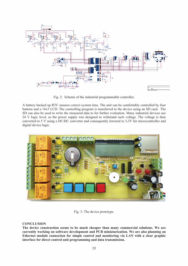
35
Fig. 2: Scheme of the industrial programmable controller. A battery backed up RTC ensures correct system time. The unit can be comfortably controlled by four buttons and a 16x3 LCD. The controlling program is transferred to the device using an SD card. The SD can also be used to write the measured data to for further evaluation. Many industrial devices use 24 V logic level, so the power supply was designed to withstand such voltage. The voltage is then converted to 5 V using a DC/DC converter and consequently lowered to 3,3V for microcontroller and digital device logic.
Fig. 3: The device prototype. CONCLUSION The device construction seems to be much cheaper than many commercial solutions. We are currently working on software development and PCB miniaturization. We are also planning an Ethernet module connection for simple control and monitoring via LAN with a clear graphic interface for direct control unit programming and data transmission.

36
SPECIAL SENSORS FOR SENSING FAST ONE-TIME EVENTS Project supervisor: Ing. Petr Drexler, Ph.D., [email protected] Project leader: Ing. Martin Friedl , [email protected] Project consultant: Ing. Michal Král , [email protected] Students: Radek Ko�í, [email protected] Project submitter: PROTOTYPA a.s., Hudcova 533 / 78c, 612 00 Brno Project submission: Familiarize with the problems of measuring the speed of moving objects with values up to 2000 m·s-1. Study the principles of existing methods and propose a new arrangement of the sensor on an inductive principle to identify fast-moving projectiles and to measure their speed. Design solutions for circumferential adjustment of the sensor signals. If necessary, use peripheral simulator for analysis of the proposed engagement. Based on the experimental design Realize sensor design and measurement verify the options and parameters. INTRODUCTION The issue of measuring the speed of moving projectiles is quite challenging because it is a one-time events, they can not be precisely repeated. Nowadays there is used of optical and electromagnetic principles and measurements using Doppler radar system. To measure the optical and electromagnetic principles are used by two gates, apart in well-defined distance, which is called the base. A single detection gates passing projectile creates a pulse that controls the fast counter. The first impulse is to run counter, we're talking about is the START pulse, and second, stop pulse, is stopped. From the obtained time interval and the known base we can calculate the average speed of a projectile on the measured section. One of the electromagnetic principles used as a gate two coils, which have primary and secondary windings. The primary winding is powered by direct current, which in the vicinity of the coil creates an electromagnetic field. When moving projectile in this field will generate eddy currents in the projectile, which creates an electromagnetic field that acts against a field in which eddy currents are excited. Field lines of force of a projectile affect the secondary coil windings, which will induce voltages and thus generate a pulse. The optical methods are mainly optical gates, which record the passage of the projectile optical beam. The light source can be a series of light emitting diodes or laser diode, whose beam is a set of mirrors to sweep the area. The PIN photodiodes are used as the photosensitive elements. During passage of the projectile will be gateway optical beam shading and the output pulse is generated. The advantage of light gates is independent of projectile material, but can not be used near the mouth, because the flash from the barrel and the departure of residual dust. Radar measurements use frequency changes reflected beam from the projectile, depending on the speed of the projectile. This measurement allows the measurement of airspeed projectile throughout its flight time. PROBLEM SOLVING For solving design sensing gates, we are decided to use the method of eddy currents induced in the projectile passing through a magnetic field coil. If we power the measure coil AC, it will generate in the surrounding magnetic field. When measured projectile (electrically conductive) motion is due to the changing magnetic field to induce eddy currents in the body of the projectile, while the size of these currents depends on the position of the projectile towards the coil, with increasing distance from the coil of a projectile the size of the eddy currents decreases. These currents create a projectile around its own magnetic field that interacts with the field coil, and thus affect the properties of the coil.
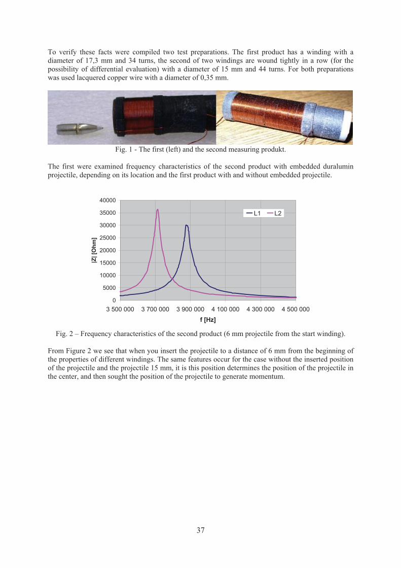
37
To verify these facts were compiled two test preparations. The first product has a winding with a diameter of 17,3 mm and 34 turns, the second of two windings are wound tightly in a row (for the possibility of differential evaluation) with a diameter of 15 mm and 44 turns. For both preparations was used lacquered copper wire with a diameter of 0,35 mm.
Fig. 1 - The first (left) and the second measuring produkt.
The first were examined frequency characteristics of the second product with embedded duralumin projectile, depending on its location and the first product with and without embedded projectile.
0
5000
10000
15000
20000
25000
30000
35000
40000
3 500 000 3 700 000 3 900 000 4 100 000 4 300 000 4 500 000
f [Hz]
|Z| [
Ohm
]
L1 L2
Fig. 2 – Frequency characteristics of the second product (6 mm projectile from the start winding).
From Figure 2 we see that when you insert the projectile to a distance of 6 mm from the beginning of the properties of different windings. The same features occur for the case without the inserted position of the projectile and the projectile 15 mm, it is this position determines the position of the projectile in the center, and then sought the position of the projectile to generate momentum.
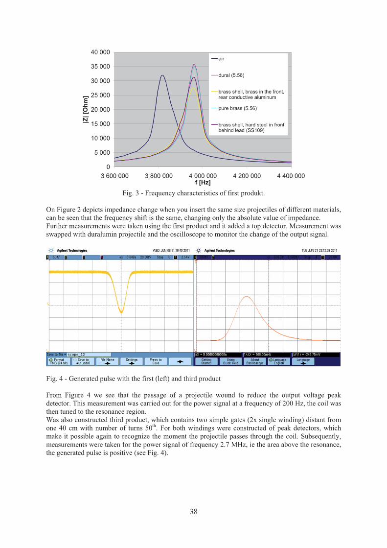
38
0
5 000
10 000
15 000
20 000
25 000
30 000
35 000
40 000
3 600 000 3 800 000 4 000 000 4 200 000 4 400 000f [Hz]
|Z| [
Ohm
]
air
dural (5.56)
brass shell, brass in the front,rear conductive aluminum
pure brass (5.56)
brass shell, hard steel in front,behind lead (SS109)
Fig. 3 - Frequency characteristics of first produkt.
On Figure 2 depicts impedance change when you insert the same size projectiles of different materials, can be seen that the frequency shift is the same, changing only the absolute value of impedance. Further measurements were taken using the first product and it added a top detector. Measurement was swapped with duralumin projectile and the oscilloscope to monitor the change of the output signal.
Fig. 4 - Generated pulse with the first (left) and third product From Figure 4 we see that the passage of a projectile wound to reduce the output voltage peak detector. This measurement was carried out for the power signal at a frequency of 200 Hz, the coil was then tuned to the resonance region. Was also constructed third product, which contains two simple gates (2x single winding) distant from one 40 cm with number of turns 50th. For both windings were constructed of peak detectors, which make it possible again to recognize the moment the projectile passes through the coil. Subsequently, measurements were taken for the power signal of frequency 2.7 MHz, ie the area above the resonance, the generated pulse is positive (see Fig. 4).
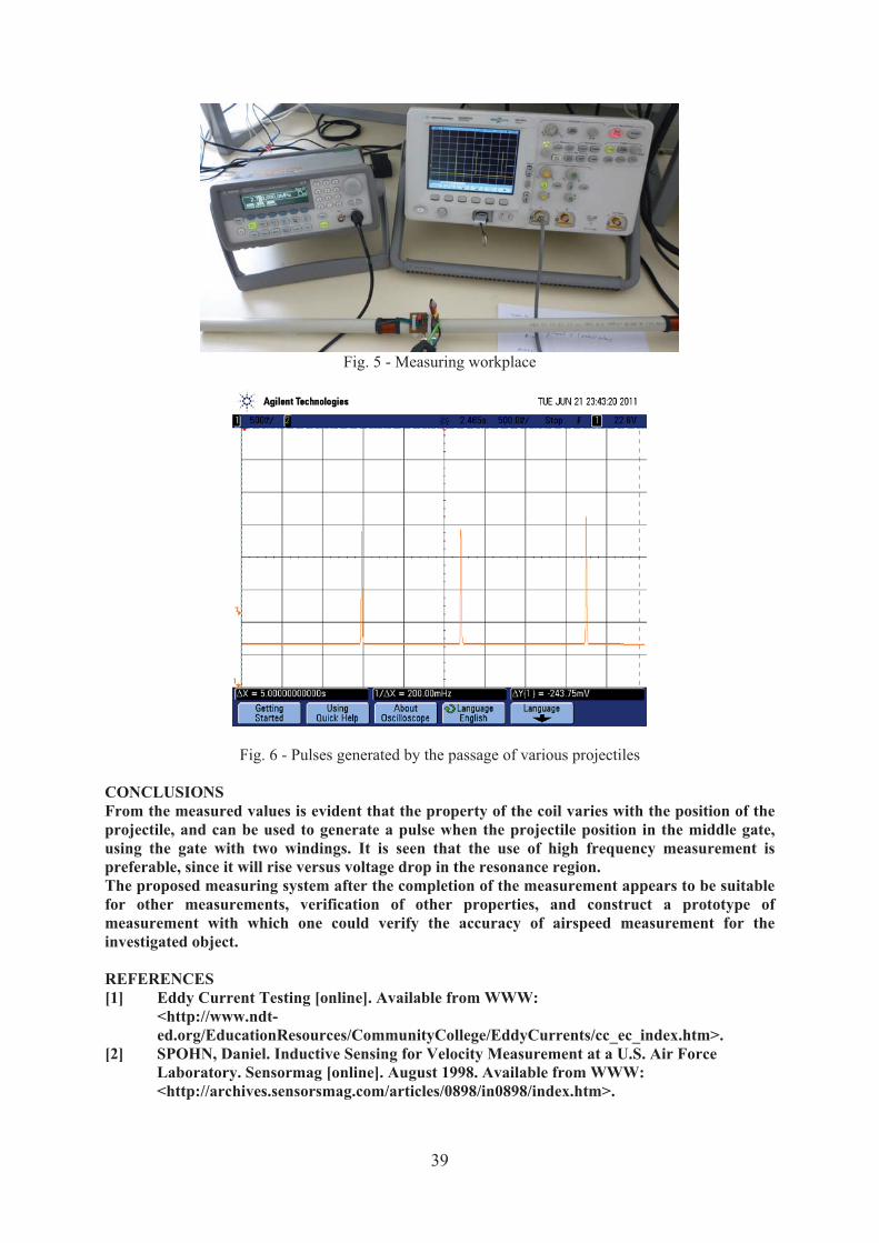
39
Fig. 5 - Measuring workplace
Fig. 6 - Pulses generated by the passage of various projectiles CONCLUSIONS From the measured values is evident that the property of the coil varies with the position of the projectile, and can be used to generate a pulse when the projectile position in the middle gate, using the gate with two windings. It is seen that the use of high frequency measurement is preferable, since it will rise versus voltage drop in the resonance region. The proposed measuring system after the completion of the measurement appears to be suitable for other measurements, verification of other properties, and construct a prototype of measurement with which one could verify the accuracy of airspeed measurement for the investigated object. REFERENCES [1] Eddy Current Testing [online]. Available from WWW:
<http://www.ndt-ed.org/EducationResources/CommunityCollege/EddyCurrents/cc_ec_index.htm>.
[2] SPOHN, Daniel. Inductive Sensing for Velocity Measurement at a U.S. Air Force Laboratory. Sensormag [online]. August 1998. Available from WWW: <http://archives.sensorsmag.com/articles/0898/in0898/index.htm>.

40
MAGNETIC FIELDS MAPPING OF SPECIFIC CONFIGURATIONS Supervizor of project: Ing. Petr Drexler, Ph.D., [email protected] Chief of project: Ing. Michal Hadinec , [email protected] Consultant of project: Michal Král , [email protected] Student: Radka Jakubíková , [email protected] Client of project: PROTOTYPA a.s., Hudcova 533 / 78c, 612 00 Brno Assignment of project: Your task is to do mapping of magnetic fields created by specific configurations of sources of magnetic fields. INTRODUCTION It is necessary to conduct an experimental specific configuration magnetic field mapping for experiments at UTEE. We take this measurements to be able to compare them with simulation in the ANSYS system. This project is concerned with the possibility of mapping the magnetic field using equipment that is available on UTEE and with realization of the mapping process on chosen magnetic fields. Normaly a magnetic transducer or probe is used for measuring a magnetic field. Such a probe transfers a measured quantity to an electric signal. It is possible to use them to measure different quantities, for example magnetic field strength, permeability, magnetic flux etc. We usually use these transducers:
� Proof coil, � Hall sensor, � Ferromagnetic probe, � Rogowski potentiometer, � Nuclear magnetic resonance.
I have used the Hall sensor for my experiment, so I will provide details only about this transducer. The Hall sensor principle is based on the Hall effect. It is the small slat (about 5 � 3 � 0,1 mm). The direct current is going through it in one way. If we put that slat into the magnetic field, the Lorentz force will affect the charged particles. This force cause that charges will deflect perpendicular to magnetic flux density. Charges are accumulate only on one side of slat, causing the Hall voltage0:
HH
R Iud�
� �B (V) (1)
where RH …Hall´s constant, (C-1.m3) I …current, (A) d …depth of the plate, (m) B …magnetic flux density, (T) The Hall voltage is proportional to magnetic flux density, while the current is constant. Then we can easily measure it by voltmeter. Hall probes can be so small that we can use them for measuring the magnetic flux density in a small air hole of ferromagnetic fields. We also can use the probe for measuring alternative magnetic field with low frequency or strong magnetic field generated by supraconductive coil. Probe always measures field that is perpendicular to slat and doesn´t have any ferromagnetic pieces, so it can´t affect the magnetic field. There are two main kinds of Hall probes - tangential and axial. The tangential probe is sensitive, on the one hand, to perpendicular magnetic field to its longitudinal axis and, on the other hand, the axial probe is sensitive to magnetic field with the same orientation as the probe´s longitudinal axis. 0
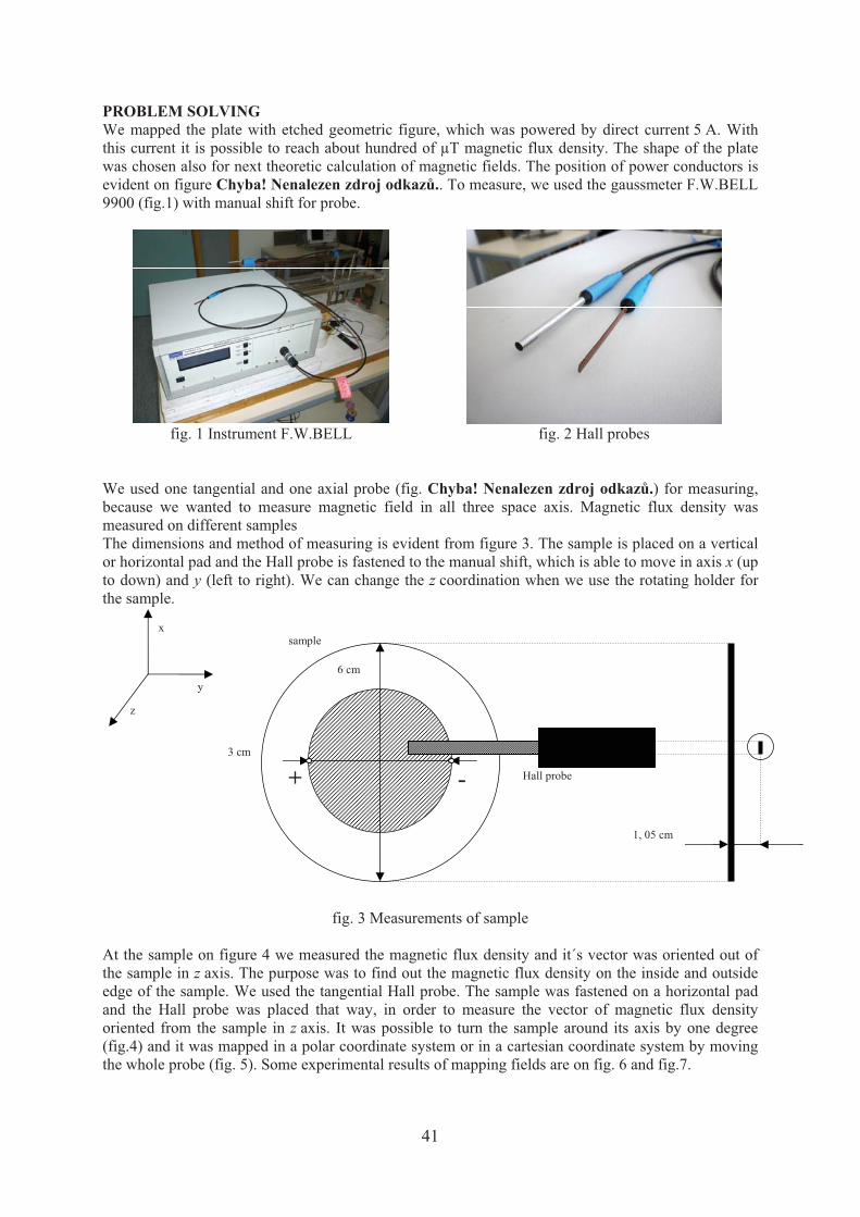
41
PROBLEM SOLVING We mapped the plate with etched geometric figure, which was powered by direct current 5 A. With this current it is possible to reach about hundred of μT magnetic flux density. The shape of the plate was chosen also for next theoretic calculation of magnetic fields. The position of power conductors is evident on figure Chyba! Nenalezen zdroj odkaz�.. To measure, we used the gaussmeter F.W.BELL 9900 (fig.1) with manual shift for probe.
fig. 1 Instrument F.W.BELL
fig. 2 Hall probes
We used one tangential and one axial probe (fig. Chyba! Nenalezen zdroj odkaz�.) for measuring, because we wanted to measure magnetic field in all three space axis. Magnetic flux density was measured on different samples The dimensions and method of measuring is evident from figure 3. The sample is placed on a vertical or horizontal pad and the Hall probe is fastened to the manual shift, which is able to move in axis x (up to down) and y (left to right). We can change the z coordination when we use the rotating holder for the sample.
fig. 3 Measurements of sample
At the sample on figure 4 we measured the magnetic flux density and it´s vector was oriented out of the sample in z axis. The purpose was to find out the magnetic flux density on the inside and outside edge of the sample. We used the tangential Hall probe. The sample was fastened on a horizontal pad and the Hall probe was placed that way, in order to measure the vector of magnetic flux density oriented from the sample in z axis. It was possible to turn the sample around its axis by one degree (fig.4) and it was mapped in a polar coordinate system or in a cartesian coordinate system by moving the whole probe (fig. 5). Some experimental results of mapping fields are on fig. 6 and fig.7.
3 cm
6 cm
Hall probe
1, 05 cm
y
x
z
+ -
sample
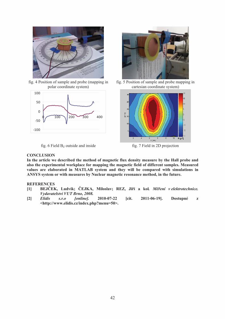
42
fig. 4 Position of sample and probe (mapping in
polar coordinate system) fig. 5 Position of sample and probe mapping in
cartesian coordinate system)
�100
�50
0
50
100
0 100 200 300 400
fig. 6 Field BZ outside and inside fig. 7 Field in 2D projection CONCLUSION In the article we described the method of magnetic flux density measure by the Hall probe and also the experimental workplace for mapping the magnetic field of different samples. Measured values are elaborated in MATLAB system and they will be compared with simulations in ANSYS system or with measures by Nuclear magnetic resonance method, in the future. REFERENCES [1] BEJ�EK, Ludvík; �EJKA, Miloslav; REZ, Ji�í a kol. M��ení v elektrotechnice.
Vydavatelství VUT Brno, 2008. [2] Elidis s.r.o [online]. 2010-07-22 [cit. 2011-06-19]. Dostupné z
<http://www.elidis.cz/index.php?menu=50>.
43
VERIFICATION OF DURABILITY AND RELIABILITY OF ELECTRONIC MODULES AND ACCELERATED TESTS Supervizor of project: doc.Ing. Petr Drexler, Ph.D., [email protected] Head of project: Ing. Michal Hadinec, Ph.D., [email protected] Ing. Zoltán Szabó., [email protected] Consultant of project: Student: Karel Nuhlí�ek, [email protected] Sponsor of project: FEI Czech republic Ltd., Podnikatelská 6, 612 00 Brno Task of the project: Reliability and mean time to failure (MTTF) of electronic modules, MTBF calculation, using practical examples from literature to create a set of basic tests (vibration, temperature cycling, high humidity) and in a short time and reveal the critical points of the proposal developed module. The specific proposal developed accelerated testing of electronic boards, verify its reliability, finding critical points / components and calculations of MTTF. INTRODUCTION This project deals with verifying the reliability and lifetime of the device or its components, using test methods and statistical calculations. Reliability of products is important so that the company can guarantee the quality of its products and thus avoid unnecessary losses, complaints and thereby reduce its prestige. Therefore it is necessary to properly test products and the resulting tests will evaluate their reliability. Among the frequently used statistical calculations include mean time to failure (MTTF), the time between failures (MTBF), tests of statistical hypotheses, and other methods of calculation. In this part of the project I will deal with the theory of reliability, accelerated testing, as well as methods of calculating the MTBF and the methods related to the reliability and statistics. The practical part of the project focuses on testing the device using specialized software, here I would like to use program called "burn-in test". In testing I will use the connection via GPIB interface with a computer on which I will use the software interface to process the results and create graphs, and report on the measurements. It is the involvement of the voltmeter and voltage source or generator with a computer. As software is used most often Agilent Vee Pro, Visual Basic, Visual C + + and various other software tools for data collection. In the last section of the project would have an overview of the functions of electronic devices and components.
Obr.1: Measuring instruments connected via GPIB.

44
PROBLEM SOLVING Basic concepts of reliability theory Reliability is focused on a specific product (object). The product is meant an element, system or its part. Each product has a moment of production from its history, it means its transport, storage, preparation for use, proper use, maintenance, repair and disposal. Of course, requires that at each stage the product was reliable. Reliability means the product's ability to perform a specified period required function under given technical conditions. We can characterize the six basic characteristics: reliability, durability, storage and security. To determine the reliability of these various types of calculations. I mention here only the main ones relating to the project.[1] MTBF (Mean Time Between Failures) It is the time between failures during operation, is designed for repairable product. It is calculated as total time on the device number of failures. Expressed by:
(1) Where is the resultant MTBF, T is the total time of operation, R is the number of failures MTTF(Mean Time To Failure) It is expressed as the total number of hours of work of all devices until the fault. Also known as the middle period of the fault. The formula to calculate the MTTF is:
(2) Where is the resulting MTTF (hours on the error), T is the total time, N is the number of units under test. For example, 10 devices are tested for 500 hours. During the test will occur two errors. The estimate for the MTBF is:
(3)
(4) Tests of statistical hypotheses This method involves testing a number of products for example total number of cars. In this test the number of cars, if these cars pass the test, we conclude that the remaining cars are functional. Tests are adjusted so that the product has met the required reliability, without irreparable damage to or defect with the product should continue to be useful when testing passes. This method is effective if the company wants to ensure a certain level of quality products, but if the product will be used different ways, it can cause a failure after a certain time. Practicle part In tests of the product is used software that is called "burn-in test". This software is commonly used for testing motherboard and its components. The program provides detailed results about the status of each of the computer. Parts of the project will be referred to the connection of voltage source and voltmeter to a computer via GPIB.
Obr.2: Block diagram of setup
Power supply
Voltmeter
PC

45
Important points of the project: Set on the source or generator voltage -1V. After DLY ms read voltmeter output voltage (DLY – time intervals) and note it to file. If the voltage is higher than +1 V to increase the voltage about 50mV Repeat from point 1. The mentioned cycle to measure the 300x. For DLY ms is necessary to set the shortest possible time as used for SW and 10 times DLY. Evaluate basic statistical indicators on the acquired sample data. To read data from the bus it is possible to use these programs: Visual Basic, Visual Studio, Agilent Vee Pro, LabVIEW, and others. CONCLUSION The article mentions basic concepts related to reliability and methods for determining the reliability of the device. I also mentioned a practical section that contains the power supply the connection of the voltmeter via GPIB to a computer with software which it is possible to read data obtained from the measuring devices and create the graph. REFERNECES [1] MARTÍNEK, Zbyn�k; HÁJEK, Josef. Teorie spolehlivosti v energetice. Univerzitní 8, 306 14 Plze : Západo�eská univerzita v Plzni, 2002. 150 s. ISBN 80-7082-894-3.

46
DESIGN OF MEASUREMENT NET Supervisor: doc. Ing. Petr Drexler, Ph.D., [email protected] Project manager: Ing. Radim Kadlec, [email protected] Consultant: Michal Král, [email protected] Student: Róbert Kraj�ír, [email protected] Submitter: PROTOTYPA a.s., Hudcova 533 / 78c, 612 00 Brno Project task: The aim of this project is to explore conception of analog measurement net for using in experiments with pulse power generator PVG-I and PVG-II. Student’s task is designed possibilities of modification recent conception measurement net with improvement of transmitting reliability on bigger distance of measurement values. Student explores possibilities of using conversion analog signal to digital signal in near area of source and at the same time save standby signal data to memory with possibilities of data transfer to computer. Student thinks about time relation of measurement signal and this knowledge use in selection of capable circumferential solution with accessible circuits. Further student peruses possibilities of transfer analog signal by optical way and find accessible device capable for realization. Possibly, student designs own realization of opto-electronic converter. INTRODUCTION The issue of measurement of electromagnetic fields in the world today is very widespread and very important. The current aspect of this issue is quite difficult to summarize these lines, because for each application is usually required a different approach. There are many measurement methods, each with their specific advantages and disadvantages, which have implications for use in some specific applications. It is therefore very difficult to choose the right method that will provide the desired benefits, and also will be sufficient to suppress its disadvantages. In solving specific problems, here at PVG waveform measurements, it is also important to know the properties and principles of the device on which we intend to carry out measurements, especially in terms of appropriate choice and implementation of measurement methods. Aim of this work is a specific measured values of the already proposed a sensor device designed to reliably transport the longer distance, while through the environment with significant interference, which occurs by radiation of electromagnetic power generated in the PVG to the surroundings. Information have to overcome a considerable distance to protect measuring device against mechanical damage and interference, since the power output of the PVG can be achieved only by using explosives and the entire measuring device when an attempt to destroy it. Important is the galvanic separation of oscilloscopes and other equipment from PVG to protect against surges in the form of voltage spikes on the line. The known solution has been used in previous experiments coaxial cable (terminated with 50 � impedance), but proved unsatisfactory in terms of interference, galvanic separation of circuits and bandwidth. It is therefore necessary to upgrade networks for measuring the above-mentioned shortcomings and find a suitable solution (and inexpensive).
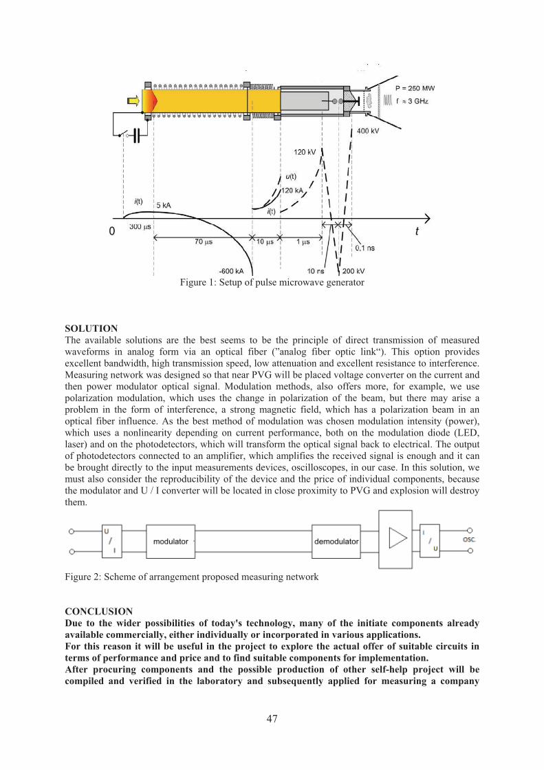
47
Figure 1: Setup of pulse microwave generator
SOLUTION The available solutions are the best seems to be the principle of direct transmission of measured waveforms in analog form via an optical fiber (”analog fiber optic link“). This option provides excellent bandwidth, high transmission speed, low attenuation and excellent resistance to interference. Measuring network was designed so that near PVG will be placed voltage converter on the current and then power modulator optical signal. Modulation methods, also offers more, for example, we use polarization modulation, which uses the change in polarization of the beam, but there may arise a problem in the form of interference, a strong magnetic field, which has a polarization beam in an optical fiber influence. As the best method of modulation was chosen modulation intensity (power), which uses a nonlinearity depending on current performance, both on the modulation diode (LED, laser) and on the photodetectors, which will transform the optical signal back to electrical. The output of photodetectors connected to an amplifier, which amplifies the received signal is enough and it can be brought directly to the input measurements devices, oscilloscopes, in our case. In this solution, we must also consider the reproducibility of the device and the price of individual components, because the modulator and U / I converter will be located in close proximity to PVG and explosion will destroy them.
Figure 2: Scheme of arrangement proposed measuring network CONCLUSION Due to the wider possibilities of today's technology, many of the initiate components already available commercially, either individually or incorporated in various applications. For this reason it will be useful in the project to explore the actual offer of suitable circuits in terms of performance and price and to find suitable components for implementation. After procuring components and the possible production of other self-help project will be compiled and verified in the laboratory and subsequently applied for measuring a company

48
Prototypa Plc.and at the Institute of Theoretical and Experimental Electrical Engineering FEEC BUT. REFERENCES [1] DREXLER P. Metody m��ení ultrakrátkých neperiodických elektromagnetických impuls�.
Ph.D. thesis. Brno: Vysoké u�ení technické v Brn�, Fakulta elektrotechniky a komunika�ních technologií, 2007. 92 s. Leader of Ph.D. thesis: doc. Ing. Pavel Fiala, Ph.D.
[2] DREXLER P. Techniky potla�ování dvojlomných jev�. Habilita�ní práce. Brno: Vysoké u�ení technické v Brn�, Fakulta elektrotechniky a komunika�ních technologií, 2009. 69 s.
[3] MYŠKA, R. M��icí systém impulzního proudového zdroje. Thesis. Brno: Vysoké u�ení technické v Brn�, Fakulta elektrotechniky a komunika�ních technologií, 2011. 79 s. Leader of thesis doc. Ing. Petr Drexler, Ph.D.

49
Preparation of Engineering Drawings for Devices Database Project supervisor: Ing. Petr Drexler, Ph.D., [email protected] Project leader: Ing. Radim Kadlec, [email protected] Consultants: Ing. Petr Slavata, [email protected] Doc. Ing. Ji�í Maxa, Ph.D., [email protected] Student: Tomáš Mejzlík, [email protected] Submitter: EATON Elektrotechnika Ltd., T�ebovská 480, 562 00 Ústí nad Orlicí, http://www.eaton.cz Submission: Solver elaborates dimensional drawings of devices in the CAD system AutoCAD according to specified rules (redrawn graphics from the product catalog into the CAD system) and prepares technical documentation. In additional solver will prepare a 3D model of selected products. Introduction The preparation was proceed in a computer application Autodesk AutoCAD 2010. Work has been separated in to four phases. In the first one it was necessary to acquaint with the principles of working in AutoCAD and the principles of technical drawing at all. An important part of this phase is understood of differences in American and European screening, as documents bases from the U.S. catalog. In the second phase, the solver met with the basic and advanced commands for two-dimensional design and then uses it to create eight variants of a 2D drawing circuit-breakers, one of them as shown in Figure 1.
Figure1: Photography of a circuit-breaker IZM To create three-dimensional model of the circuit breaker, it was essential to examine the issue of designing in three dimensions and necessary principles associated with it. It was necessary to learn work with three-dimensional formations and commands, and created 3D models. The last, most time consuming part of this project was the application of circuit breakers in a switchboard and modeled cables, busbars, brackets, mountings, and similar devices strictly necessary for real operation of power circuit breakers in switchboards. Realization Part of the work has been made in 2D and it was therefore necessary to adapt principles of two-dimensional drawings. Planar design is similar to technical drawing on paper. To draw all the 2D drawings in this project, it would be suffice to use just two basic formations - line and circle. But for higher efficiency student also used rectangles, polygons, and polyline.
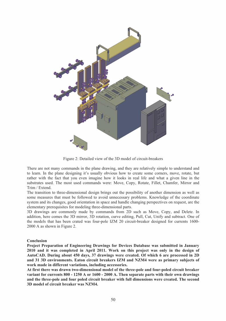
50
Figure 2: Detailed view of the 3D model of circuit-breakers There are not many commands in the plane drawing, and they are relatively simple to understand and to learn. In the plane designing it’s usually obvious how to create some corners, move, rotate, but rather with the fact that you even imagine how it looks in real life and what a given line in the substrates used. The most used commands were: Move, Copy, Rotate, Fillet, Chamfer, Mirror and Trim / Extend. The transition to three-dimensional design brings out the possibility of another dimension as well as some measures that must be followed to avoid unnecessary problems. Knowledge of the coordinate system and its changes, good orientation in space and handle changing perspectives on request, are the elementary prerequisites for modeling three-dimensional parts. 3D drawings are commonly made by commands from 2D such as Move, Copy, and Delete. In addition, here comes the 3D mirror, 3D rotation, curve editing, Pull, Cut, Unify and subtract. One of the models that has been crated was four-pole IZM 20 circuit-breaker designed for currents 1600-2000 A as shown in Figure 2. Conclusion Project Preparation of Engineering Drawings for Devices Database was submitted in January 2010 and it was completed in April 2011. Work on this project was only in the design of AutoCAD. During about 450 days, 37 drawings were created. Of which 6 are processed in 2D and 31 3D environments. Eaton circuit breakers IZM and NZM4 were as primary subjects of work made in different variations, including accessories. At first there was drawn two-dimensional model of the three-pole and four-poled circuit breaker variant for currents 800 - 1250 A or 1600 - 2000 A. Then separate parts with their own drawings and the three-pole and four poled circuit breaker with full dimensions were created. The second 3D model of circuit breaker was NZM4.

51
Circuit breakers were stored in a switchboard and a real connection to busbars, power cables were modeled for them. Connecting the circuit breakers was processed in a more variants for top and back of the busbars. Model of three-pole circuit breakers has been incorporated into the cabinet in the options: circuit breaker through the door - the upper bus, circuit breaker through the door - the back bus, the circuit breaker at the door - the upper bus, circuit breaker at the door - the back bus. Each of the variant is available with views of open and closed doors. NZM4 model is available also with open doors and closures in the back and upper versions busbars. REFERENCES �SN ISO 129-1. Technické výkresy : Kótování a tolerování. [s.l.] : Czech Standards Institute, August 2005. 32 s. Catalogue No. 73718. Catalogue. TOP Servis - Kabelové p�íchytky SONAP. Brno : TOP Servis, January 2010. 3 s. Available on www: <http://www.topservisbrno.cz/files/dokumenty/TOPservis_katalog_SONAP.pdf>. �SN EN 60898-1. Elektrická p�íslušenství : Jisti�e pro nadproudové jišt�ní domovních a podobných instalací - �ást 1: Jisti�e pro st�ídavý provoz (AC). Prague : Czech Standards Institute, November 2003. 112 s. Catalogue No.: 68639. FO�T, Petr; KLETE�KA, Jaroslav. AutoCAD 2010 : U�ebnice. Brno : Computer Press, November 2009. 384 s. ISBN 978-80-251-2181-8.

52
DESIGN OF LOW VOLTAGE SWITCHGEAR Supervisor: prof. Ing. Jarmila D�dková, CSc., [email protected] Project manager: Ing. Radim Kadlec, [email protected] Consultant: Ing. Petr Slavata, [email protected] Student: Štefan Róža, [email protected] Submitter: EATON Elektrotechnika Ltd., T�ebovská 480, 562 00 Ústí nad Orlicí, http://www.eaton.cz Project task: Design of low voltage switchgear for industrial building (design of protective devices, switchgear design). Based on the given diagram solver performs short-circuit calculations in the PAVOUK (a program for designing networks with low-voltage protection devices Eaton / Moeller) and propose appropriate protective devices. Then will design cabinets in the M-profile (a program for designing cabinets Eaton / Moeller). For the supply management field suggests main circuit and creates a 3D model. In conclusion, prepare technical documentation. INTRODUCTION My task in the project is the reconstruction of an existing substation project NN. The work includes modification of the project substation according to the applicable standards in AutoCAD, then put the project into PAVOUK and calculates short-circuit currents and thus determines all the bus wires and other elements. Finally it is design switchgear in the M-profile. Received (incorrect) scheme of low voltage switchgear in dwg format includes two switchgears for 3 fields. The scheme was chaotic, not divided into levels, which determines the clarity and expertise of project distribution, brands, and were connected by joints, and most elements have been offset. Brands have different sizes and were not the same. It was made the division of fields and bonding of individual fields. Furthermore, the scheme lacked the power of the UPS (back-up power during power failure). To the first solution, thus modifying the diagram I made in AutoCAD.
Figr. 1: Part of the wrong scheme, AUTOCAD SOLUTION Modification of scheme I started aligning brands and linking unfinished joints. This helped me function AutoCAD - extend. I added a border fields and modified their definition. I aligned the different elements and I could continue the treatment and distribution levels. Layers are important, the project is so clear and levels are helpful when editing and printing project. At the beginning I had to realize the structure diagram, divide the power circuits and controls, to determine the bus. I created levels, I have collectively called elements belonging to one level and assigned them. Each of the levels I have assigned sublevels to be defined names, descriptions and links. I continued to link the fields.
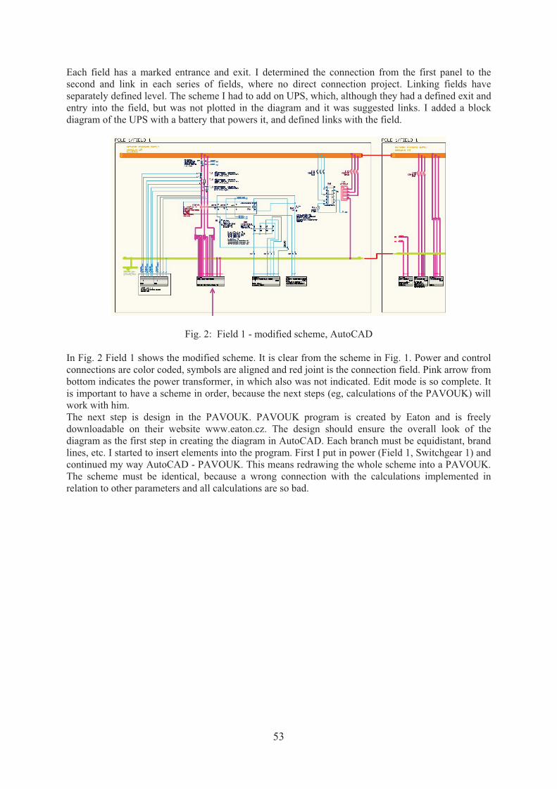
53
Each field has a marked entrance and exit. I determined the connection from the first panel to the second and link in each series of fields, where no direct connection project. Linking fields have separately defined level. The scheme I had to add on UPS, which, although they had a defined exit and entry into the field, but was not plotted in the diagram and it was suggested links. I added a block diagram of the UPS with a battery that powers it, and defined links with the field.
Fig. 2: Field 1 - modified scheme, AutoCAD In Fig. 2 Field 1 shows the modified scheme. It is clear from the scheme in Fig. 1. Power and control connections are color coded, symbols are aligned and red joint is the connection field. Pink arrow from bottom indicates the power transformer, in which also was not indicated. Edit mode is so complete. It is important to have a scheme in order, because the next steps (eg, calculations of the PAVOUK) will work with him. The next step is design in the PAVOUK. PAVOUK program is created by Eaton and is freely downloadable on their website www.eaton.cz. The design should ensure the overall look of the diagram as the first step in creating the diagram in AutoCAD. Each branch must be equidistant, brand lines, etc. I started to insert elements into the program. First I put in power (Field 1, Switchgear 1) and continued my way AutoCAD - PAVOUK. This means redrawing the whole scheme into a PAVOUK. The scheme must be identical, because a wrong connection with the calculations implemented in relation to other parameters and all calculations are so bad.
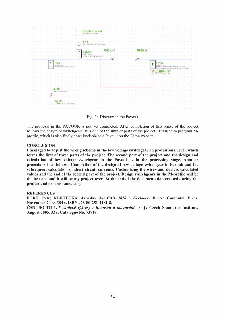
54
Fig. 3: Diagram in the Pavouk The proposal in the PAVOUK is not yet completed. After completion of this phase of the project follows the design of switchgears. It is one of the simpler parts of the project. It is used to program M-profile, which is also freely downloadable as a Pavouk on the Eaton website. CONCLUSION I managed to adjust the wrong scheme in the low voltage switchgear on professional level, which forms the first of three parts of the project. The second part of the project and the design and calculation of low voltage switchgear in the Pavouk is in the processing stage. Another procedure is as follows. Completion of the design of low voltage switchgear in Pavouk and the subsequent calculation of short circuit currents. Customizing the wires and devices calculated values and the end of the second part of the project. Design switchgears in the M-profile will be the last one and it will be my project over. At the end of the documentation created during the project and process knowledge. REFERENCES FO�T, Petr; KLETE�KA, Jaroslav. AutoCAD 2010 : U�ebnice. Brno : Computer Press, November 2009. 384 s. ISBN 978-80-251-2181-8. �SN ISO 129-1. Technické výkresy : Kótování a tolerování. [s.l.] : Czech Standards Institute, August 2005. 32 s. Catalogue No. 73718.
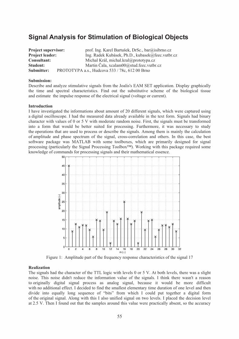
55
Signal Analysis for Stimulation of Biological Objects Project supervisor: prof. Ing. Karel Bartušek, DrSc., [email protected] Project leader: Ing. Radek Kubásek, Ph.D., [email protected] Consultant: Michal Král, [email protected] Student: Martin �ala, [email protected] Submitter: PROTOTYPA a.s., Hudcova 533 / 78c, 612 00 Brno Submission: Describe and analyze stimulative signals from the Joalis's EAM SET application. Display graphically the time and spectral characteristics. Find out the substitutive scheme of the biological tissue and estimate the impulse response of the electrical signal (voltage or current). Introduction I have investigated the informations about amount of 20 different signals, which were captured using a digital oscilloscope. I had the measured data already available in the text form. Signals had binary character with values of 0 or 5 V with moderate random noise. First, the signals must be transformed into a form that would be better suited for processing. Furthermore, it was necessary to study the operations that are used to process or describe the signals. Among them is mainly the calculation of amplitude and phase spectrum of the signal, cross-correlation and others. In this case, the best software package was MATLAB with some toolboxes, which are primarily designed for signal processing (particularly the Signal Processing Toolbox™). Working with this package required some knowledge of commands for processing signals and their mathematical essence.
Figure 1: Amplitude part of the frequency response characteristics of the signal 17
Realization The signals had the character of the TTL logic with levels 0 or 5 V. At both levels, there was a slight noise. This noise didn't reduce the information value of the signals. I think there wasn't a reason to originally digital signal process as analog signal, because it would be more difficult with no additional effect. I decided to find the smallest elementary time duration of one level and then divide into equally long sequence of “bits” from which I could put together a digital form of the original signal. Along with this I also unified signal on two levels. I placed the decision level at 2.5 V. Then I found out that the samples around this value were practically absent, so the accuracy
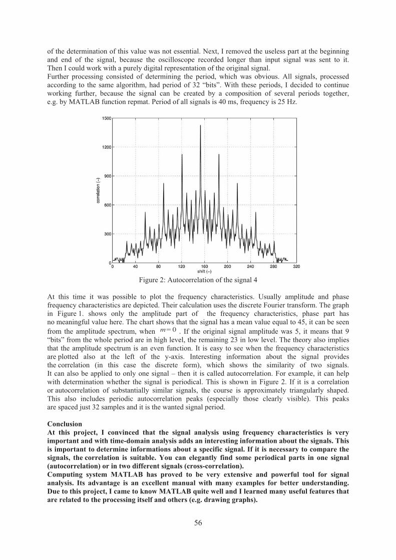
56
of the determination of this value was not essential. Next, I removed the useless part at the beginning and end of the signal, because the oscilloscope recorded longer than input signal was sent to it. Then I could work with a purely digital representation of the original signal. Further processing consisted of determining the period, which was obvious. All signals, processed according to the same algorithm, had period of 32 “bits”. With these periods, I decided to continue working further, because the signal can be created by a composition of several periods together, e.g. by MATLAB function repmat. Period of all signals is 40 ms, frequency is 25 Hz.
Figure 2: Autocorrelation of the signal 4
At this time it was possible to plot the frequency characteristics. Usually amplitude and phase frequency characteristics are depicted. Their calculation uses the discrete Fourier transform. The graph in Figure 1. shows only the amplitude part of the frequency characteristics, phase part has no meaningful value here. The chart shows that the signal has a mean value equal to 45, it can be seen from the amplitude spectrum, when m= 0 . If the original signal amplitude was 5, it means that 9 “bits” from the whole period are in high level, the remaining 23 in low level. The theory also implies that the amplitude spectrum is an even function. It is easy to see when the frequency characteristics are plotted also at the left of the y-axis. Interesting information about the signal provides the correlation (in this case the discrete form), which shows the similarity of two signals. It can also be applied to only one signal – then it is called autocorrelation. For example, it can help with determination whether the signal is periodical. This is shown in Figure 2. If it is a correlation or autocorrelation of substantially similar signals, the course is approximately triangularly shaped. This also includes periodic autocorrelation peaks (especially those clearly visible). This peaks are spaced just 32 samples and it is the wanted signal period. Conclusion At this project, I convinced that the signal analysis using frequency characteristics is very important and with time-domain analysis adds an interesting information about the signals. This is important to determine informations about a specific signal. If it is necessary to compare the signals, the correlation is suitable. You can elegantly find some periodical parts in one signal (autocorrelation) or in two different signals (cross-correlation). Computing system MATLAB has proved to be very extensive and powerful tool for signal analysis. Its advantage is an excellent manual with many examples for better understanding. Due to this project, I came to know MATLAB quite well and I learned many useful features that are related to the processing itself and others (e.g. drawing graphs).

57
REFERENCES MathWorks, Inc. MATLAB - Documentation [online]. 2011 [cited 2011 Aug 21]. Available from: <http://www.mathworks.com/help/techdoc/>. JURA, Pavel. Signály a systémy : Diskrétní signály a diskrétní systémy . Second updated edition. Brno : [s.n.], 2010. 87 p.

58
PRACTICAL IMPLEMENTATIO OF NOISE GENERATOR Project supervisor: prof. Ing. Karel Bartušek, DrSc., [email protected] Project leader: Ing. Radek Kubásek, Ph.D., [email protected] Project consultant: Michal Král, [email protected] Student: Petr Frenštátský ([email protected] Project submitter: PROTOTYPA a.s., Hudcova 533 / 78c, 612 00 Brno Project submission: The aim of the project is to implement noise generator in one or more copies and different properties. Students will become familiar with different sources of noise based on different physical principles. On the basis of theoretical knowledge will be made predictable noise generator design features. Properties will be verified experimentally generated noise. The basic parameters of the desired properties are mainly the frequency range and noise performance, its randomness and color. INTRODUCTION The term noise can introduce a parasitic phenomenon that appears in the spectrum of the signal and affects the result. Noise can also be seen as a useful phenomenon. Noise characteristics occur practically in all the electronic components, depending on the rate of radiation. It is influenced by the way how the noise is created, based on the physical properties of components. The most typical kind of noise is thermal, which is appears in all components based on resistive character. Another way is shot radiation noise, which is characteristic of semiconductor devices. It is caused leakage DC current through a semiconductor, which occur randomly and recombining electron-hole pairs. Noise can also be characterized by its color, which came approximately from analogies between the frequency spectrum and the spectrum of colored light. This includes for example, white noise, pink noise, black noise, etc. The project aims to create a noise signal whose spectrum will correspond to white noise. White noise is characterized by its power spectral density. Sections with the same wide frequency band have the same energy throughout the whole spectrum.
Fig. 1: Noise signal
PROBLEM SOLVING The first task of the project is to summarize the theoretical knowledge of noises. It is a mathematical description of the noise, way of creation or characterization of coloring. The basic electronic components that produce white noise are Zener diode connected in reverse. The diode noise arises due shot or snowball effect. This is due to the characteristics of large discontinuities in the transition from blocking to conducting state diode, thereby causing the occurrence micro-breakdowns. At higher current values the breakdown becomes a stable and noise disappear. The amplitude noise can reach levels of up to several mV. One objective of the project is to find the best diode, which shows the best properties. It is mainly about his color. Since it is best to find a white noise generator, it must satisfy the constant power spectral density is constant.
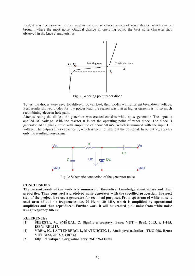
59
First, it was necessary to find an area in the reverse characteristics of zener diodes, which can be brought where the most noise. Gradual change in operating point, the best noise characteristics observed in the knee characteristics.
Fig. 2: Working point zener diode
To test the diodes were used for different power load, then diodes with different breakdown voltage. Best results showed diodes for low power load, the reason was that at higher currents is no so much recombining electron-hole pairs. After selecting the diodes, the generator was created consists white noise generator. The input is applied DC voltage. With the resistor R is set the operating point of zener diode. The diode is generated AC signal - noise with amplitude of about 50 mV, which is summed with the input DC voltage. The outputs filter capacitor C, which is there to filter out the dc signal. In output Vn, appears only the resulting noise signal.
Fig. 3: Schematic connection of the generator noise
CONCLUSIONS The current result of the work is a summary of theoretical knowledge about noises and their properties. Then construct a prototype noise generator with the specified properties. The next step of the project is to use a generator for technical purposes. From spectrum of white noise is used area of audible frequencies, i.e. 20 Hz to 20 kHz, which is amplified by operational amplifiers and then reproduced. Further work it will be created pink noise from white noise using frequency filters. REFERENCES [1] ŠEBESTA, V., SMÉKAL, Z. Signály a soustavy. Brno: VUT v Brn�, 2003. s. 1-165.
ISBN: REL117. [2] VRBA, K., LATTENBERG, I., MATJÍ�EK, L. Analogová technika - TKO 008. Brno:
VUT Brno, 2002. s. (107 s.) [3] http://cs.wikipedia.org/wiki/Barvy_%C5%A1umu
Blocking state Conducting state

60
SENSORS FOR SHORT HIGH LEVEL CURRENT IMPULSE Project supervisor: doc. Ing. Petr Drexler, Ph.D., [email protected] Project leader: Ing. Radek Kubásek, Ph.D., [email protected] Project consultant: Michal Král , [email protected] Student: Bc. Radek Myška, [email protected] Project authority: PROTOTYPA a.s., Hudcova 533 / 78c, 612 00 Brno Task of project: The request is placed on a high cutoff frequency transducer, galvanic isolation sensor from the test equipment and resistance against external electromagnetic interference. The selected solution will by realized and verified on the test pulse source with these parameters Pmax = 80 MW, Imax = 4 kA, tp = 100 ns. INTRODUCTION The issues measurement of short current pulses of several units as far as thousands of kiloamps with duration of several units as far as hundreds nanoseconds is at the present actual due the raising usage of high-level pulse current sources occurs. Examples are application in physical research, technological applications, building and food processing industry or in the medicine [1]. The most powerful source are able to generate impulses with peak value current 100 MA with overall power 100 TW [1]. Designed sensor must have sufficiently large frequency band width and suitable sensitivity. Further sensor must by resistant toward electromagnetic interference. ROGOWSKI SENSOR (COIL) This sensor is based on Ampére’s law of the total current a Faraday’s law of induction. Sensor is constructed like coil with air core with a defined numbers of turns wound around carrier construction.
ui
d ( )di tI
t�
figure 1. a) Rogowski coil like sensor current b) circuit model of Rogowski sensor with load resistance
RL The output voltage is proportional of the time derivate of the measured current. To obtain current waveform is necessary integrate. For integration can by used self-integration when the sensor is loaded resistance with low value, the instantaneous value of the output voltage uo(t) is then equal to the instantaneous value of the measured current i(t). In experimental measurement on the PFL has been indentified three major phenomena that limit the use of the Rogowski sensor for measuring very short non-harmonic current waveforms. The first is the fact that it is necessary to consider as a sensor circuit with distributed parameters. For correct measurement of non-harmonic waveform is necessary to ensure the Heaviside condition for distortionless line. The second factor is the Gibbs phenomenon causing overshoots on the rising edges. The third factor is the influence of the position wire in the coil to the output waveform. MAGNETO-OPTICAL SENSOR Magneto-optical sensor based on magneto-optical Faraday effect. The phenomenon occurs in optically active substances in the longitudinal magnetic field is to decant the plane of polarization of light waves figure 2a). For the dependence twisted plane angle polarization � depending on the size of the magnetic induction field B and interaction length l can be derived equation [2] ,VBl VHl� �� � (1) where V is the Verdet constant that characterizes the magneto-optical properties of the environment.
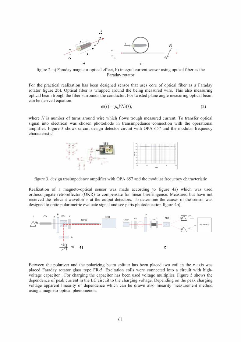
61
I
E1 E2
�
figure 2. a) Faraday magneto-optical effect, b) integral current sensor using optical fiber as the
Faraday rotator For the practical realization has been designed sensor that uses core of optical fiber as a Faraday rotator figure 2b). Optical fiber is wrapped around the being measured wire. This also measuring optical beam trough the fiber surrounds the conductor. For twisted plane angle measuring optical beam can be derived equation. 0( ) ( ),t VNi t� �� (2) where N is number of turns around wire which flows trough measured current. To transfer optical signal into electrical was chosen photodiode in transimpedance connection with the operational amplifier. Figure 3 shows circuit design detector circuit with OPA 657 and the modular frequency characteristic.
0
10
20
30
40
50
60
70
0,01 0,1 1 10 100
f[MHz]
U2[
dB]
figure 3. design trasimpedance amplifier with OPA 657 and the modular frequency characteristic
Realization of a magneto-optical sensor was made according to figure 4a) which was used orthoconjugate retroreflector (OKR) to compensate for linear birefringence. Measured but have not received the relevant waveforms at the output detectors. To determine the causes of the sensor was designed to optic polarimetric evaluate signal and see parts photodetection figure 4b).
L OV KP
DS KOV-S
OKR
A
FD
Laser �/4
PFD
FD
osciloskop
PBSL FRL
Between the polarizer and the polarizing beam splitter has been placed two coil in the x axis was placed Faraday rotator glass type FR-5. Excitation coils were connected into a circuit with high-voltage capacitor . For charging the capacitor has been used voltage multiplier. Figure 5 shows the dependence of peak current in the LC circuit to the charging voltage. Depending on the peak charging voltage apparent linearity of dependence which can be drawn also linearity measurement method using a magneto-optical phenomenon.
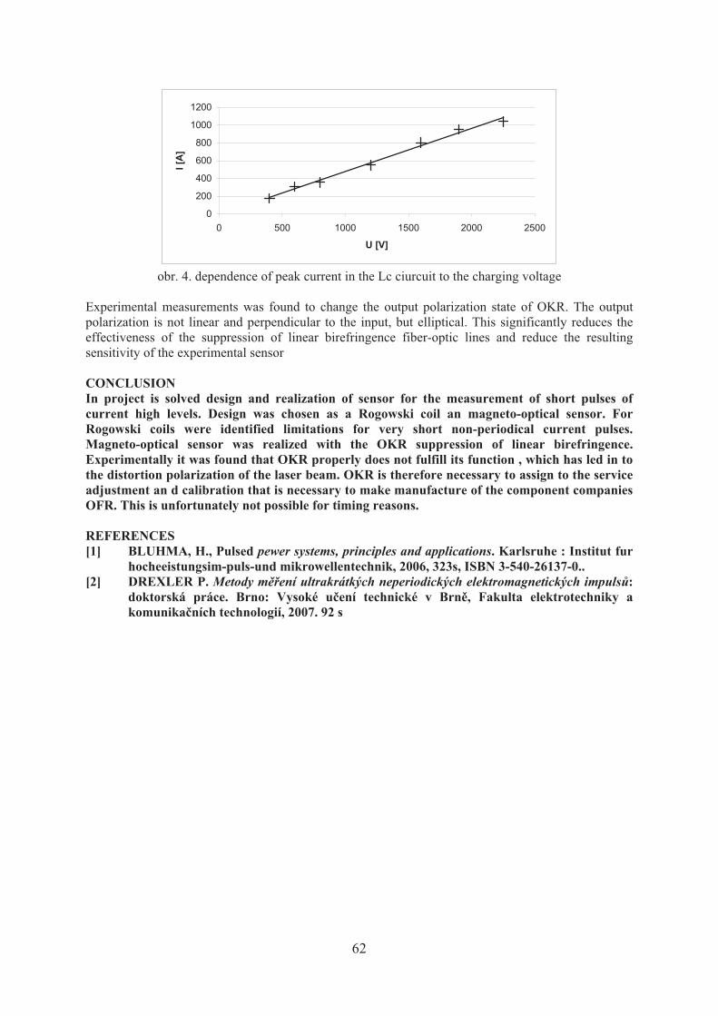
62
0
200
400
600
800
1000
1200
0 500 1000 1500 2000 2500
U [V]
I [A
]
obr. 4. dependence of peak current in the Lc ciurcuit to the charging voltage
Experimental measurements was found to change the output polarization state of OKR. The output polarization is not linear and perpendicular to the input, but elliptical. This significantly reduces the effectiveness of the suppression of linear birefringence fiber-optic lines and reduce the resulting sensitivity of the experimental sensor CONCLUSION In project is solved design and realization of sensor for the measurement of short pulses of current high levels. Design was chosen as a Rogowski coil an magneto-optical sensor. For Rogowski coils were identified limitations for very short non-periodical current pulses. Magneto-optical sensor was realized with the OKR suppression of linear birefringence. Experimentally it was found that OKR properly does not fulfill its function , which has led in to the distortion polarization of the laser beam. OKR is therefore necessary to assign to the service adjustment an d calibration that is necessary to make manufacture of the component companies OFR. This is unfortunately not possible for timing reasons. REFERENCES [1] BLUHMA, H., Pulsed pewer systems, principles and applications. Karlsruhe : Institut fur
hocheeistungsim-puls-und mikrowellentechnik, 2006, 323s, ISBN 3-540-26137-0.. [2] DREXLER P. Metody m��ení ultrakrátkých neperiodických elektromagnetických impuls�:
doktorská práce. Brno: Vysoké u�ení technické v Brn�, Fakulta elektrotechniky a komunika�ních technologií, 2007. 92 s

63
AUTOMATIC TEST LINE SUGGESTION Project supervizor: Ing. Petr Drexler, Ph.D., [email protected] Project leader: Ing. Jan Mikulka, [email protected] Project consultant: Ing. Radek Javora, [email protected] Students: Ond�ej Brýdl, [email protected] Ales Czudek, [email protected] Stanislav Goryl, [email protected] Filip Haring, [email protected] Jakub Hezcko, [email protected] Project orderer: ABB Ltd., Víde�ská 117, 619 00 Brno Project task: Meet the procedures for testing precision electronic senzors current and voltage and procedures of the piece trials. Study the qualitative and quantitative parameters of testing current and voltage, according to standard (IEC 60044-7, IEC 60044-8 a IEC 61869-1). Discuss various possibilities of realization needed trials on one testing, in ordered to reduce time of measuring. Suggest appropriate ordering place for current measuring all parameters. At the suggestion consider possible mutual influence for realization of particular trials and approximate price. Suggestion needs to accomplish safety rules, keep the precision and quality of current trials. In case of needs work out more possible solutions and compare their qualities. INTRODUCTION Project task is to make up and suggest automatic line for measuring on sensors. Output trials is used for exposure defect created during the production. Suggestion automatic line is created with ABB company. The purpose is mainly about making the measuring faster. Automatic line is designed with consideration room size and using maximum present equipment. In this way initial expense are reduced to the minimum. Automatic line must be designed for all types electronic transformers which ABB produces. For future development must be easy to add another type, automatic line must be adaptable. Testing workplace will be independent system, where men don´t have to be involved. One person is enough to control all measuring, instead of three as it used to be. SUGGESTION OF THE SOLUTION Production tests of transformers consist of: Insulation test of the secondary conduit, test to measure the C1 capacity (capacity between the primary winding and the resistance on the
output sensors), test to measure the C2 capacity (capacity of measurement sensor to ground),
measurement of partial discharges, insulation test of the primary conduit, measurement of voltage accuracy, measurement of current accuracy.
Picture 1 Unit for all the types of senzors

64
Size of unit is 60x30x20 cm. From inside is located connector RJ-45 and three others cable for connecting to sensor. From outside is placed ten measuring spots. Measuring needles will arrived to them for testing. In the unit are created recess for sensor KEVCD or extension for another type(pic. 2).
Picture 2 Illustration of extension for type KERC
In picture 3 are three measuring stations, first measure three tests -– - insulation test of the secondary conduit, test to measure the C1 capacity and the C2 capacity. Second station measured two tests - - insulation test of the primary conduit and measurement of partial discharges. Third station making rest of tests - measurement of voltage and current accuracy. Measuring is perform in this way: Operator insert sensor to unit, connect to unit and move it to drive part on track. Unit is stopped in first station, with device on the side is making stabilization position. Senzor RIFD code is read by station and according to RFID are perform tests. Secundary circuit is contacted by measuring needle, primary circuit by robotic arm. After that is executed measuring, save the results and sensor move to another station.
Picture 3 Illustration of automatic line for measuring

65
Table 1 Compare number of measured senzors
�� Speed� of� completed�measured�senzors�
Number� of� completely�measured�senzors�in�1�hour�
Number� of� completely�measured�senzors�in�8�hour�
��Whit capacity detector
Whit-out capacity detector
Whit capacity detector
Whit-out capacity detector
Whit capacity detector
Whit-out capacity detector
Present�state� 7�minut� 6�minut���30�vte�in 5� 6� 39� 42�
Automatic�line�
3�minuty��30�vte�in�
2�minuty��30�vte�in 17� 25� 136� 200�
CONSLUSION Suggestion of automatic line is realized by IET2 project and company ABB. In created this suggestion must be know standard �SN about measuring on transformers and also business convention in ABB. Within project was simulated measured with unit, to compare degradation with or with-out unit. The result of the project is specific suggest on automatic measuring line, with all requirements and advantage against actual state. REFERENCES [1] ZEZULKA, F. PROST�EDKY PR�MYSLOVÉ AUTOMATIZACE. VUTIUM. VUTIUM. BRNO: VUTIUM, 2004. 176 S. ISBN 8021426101. [2] GESCHEIDTOVÁ, E., REZ, J., STEINBAUER, M. M�ENÍ V ELEKTROTECHNICE. M�ENÍ V ELEKTROTECHNICE. BRNO: VUTIM, 2002. S. (184 S.)ISBN: 8021419903. [3] �SN EN 61869-1. P�ÍSTROJOVÉ TRANSFORMÁTORY: �ÁST 1: VŠEOBECNÉ POŽADAVKY. [S.L.]: Ú�AD PRO TECHNICKOU NORMALIZACI, METROLOGII A ZKUŠEBNICTVÍ, DUBEN 2010. 62 S.

66
Optimization of methods for image noise suppression Project supervisor: prof. Ing. Karel Bartušek, DrSc. Project manager: Ing. Jan Mikulka Student: Kryštof Chotaš The sponsor of the project: PROTOTYPA a.s., Hudcova 533 / 78c, 612 00 Brno Main task of project: Aim of this project is to construct suitable method for image noise suppression in images of 3D MRI. Introduction: Magnetic resonance imaging (MRI) From a historical perspective is quite new technology, known from 1940's, which has been using in medicine since 1970's, to diagnose medical problems. This method is based on placing nucleus into constant magnetic field B1 and it perpendicular (transversal) high-frequency field B2(MHz), which is causing permanent core rotation in the XY plane. It is quite easy to know, which nucleus will be in resonance, by choosing the force of magnetic fields (B1 ,B2). After turning of field B2, nucleus still rotate in XY plane and induce voltage in measuring coil. This voltage is used to determine required values. It is necessary to say, that MRI is only connected with odd mass number elements. The best for measurement is hydrogen atom with only one proton, so it has large magnetic moment and there is also about 60% of body-mass consisting of hydrogen. MRI is widely used in practice mainly due to the following advantages. Ex.: There are no demonstrable negative effect of MRI, by standard hygienic conditions and it is also more precise and superior then other methods. Their advantage is also that, we can create an entire model of the object with a sufficient number of images. Three-dimensional diagnosis by MRI It is obvious, that we need three coordinates, to determine the position in space. The MRI is calculated by using the gradients. The width of the cut determines the slice selecting gradient, which consists of a magnetic field with increasing intensity according to the axis of the object, where the individual images are chosen by the appropriate frequency. Then we have a field perpendicular to this axis, which determines the readout gradient. And finally, we determine the final coordinates from phase encoding gradient. Note: This is a very brief outline about MRI and it is important to study more literature for complete understanding,. Noise in 3D MRI pictures: As I already mention, the 3D MRI (next only MRI) is frequently used in medicine to determine diagnoses. It is necessary to get the best detailed description of the investigated object (brain, aorta cross-section, etc.) for precise diagnosis. Unfortunately, MRI images are often affected by large noise, which is also proportional to signal level, local proton density, bandwidth, system design, quality of RF coil and in particular on scanning parameters. In general noise suppression in MRI images occurs fundamental problem, that the noise is in the same frequency band as the details of the image. For this reason, it is necessary to find a suitable compromise between the smoothing and suppressing the signal noise, and loss of detail on the other side (the SNR ratio). To achieve great detail for creating a 3D model, we can increase the number of images by thickness of slice. Unfortunately, narrowing of the thickness of slice makes more noise and that cause the loss of information (worsening SNR ratio). So we decided to find a suitable compromise between slice thickness and the amount of noise and we came to solution, that might be appropriate to calculate some of the images.
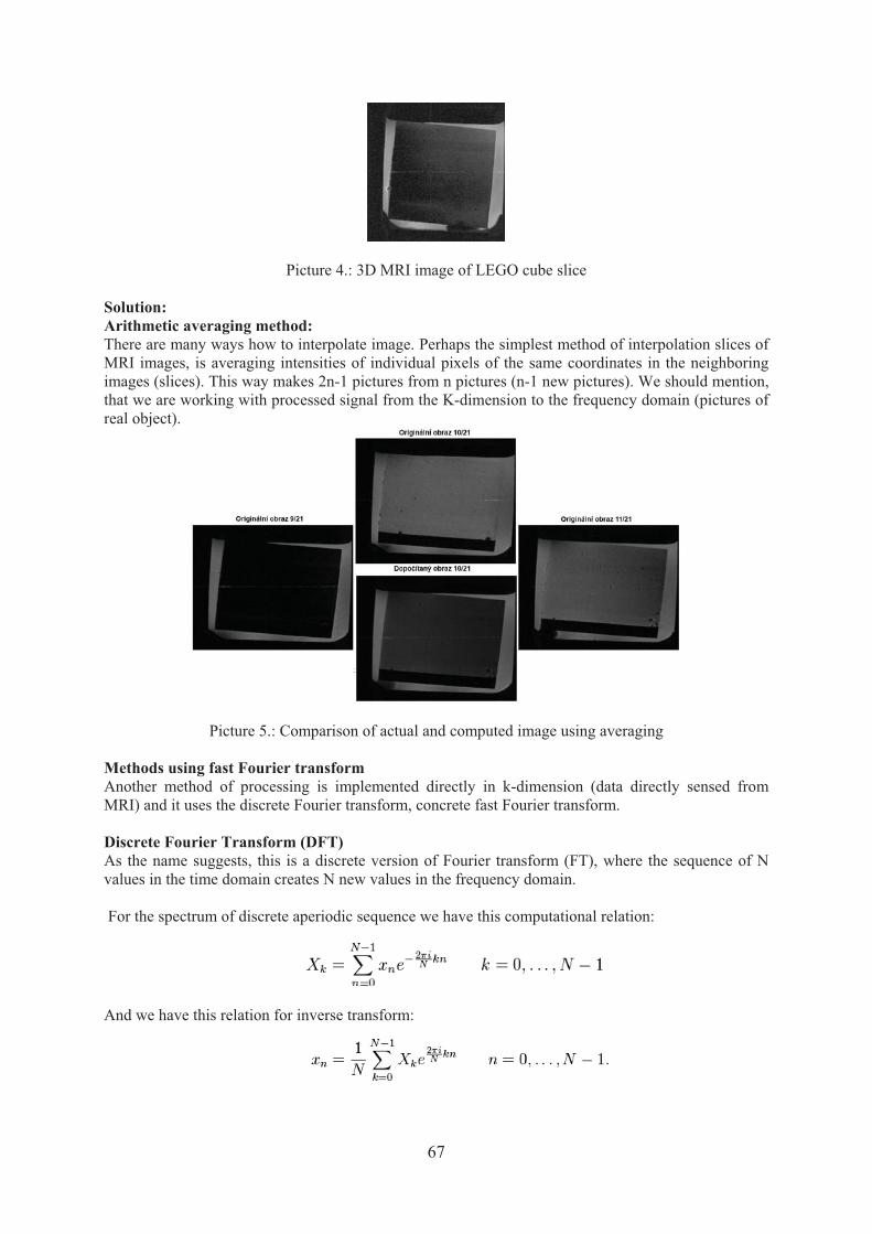
67
Picture 4.: 3D MRI image of LEGO cube slice Solution: Arithmetic averaging method: There are many ways how to interpolate image. Perhaps the simplest method of interpolation slices of MRI images, is averaging intensities of individual pixels of the same coordinates in the neighboring images (slices). This way makes 2n-1 pictures from n pictures (n-1 new pictures). We should mention, that we are working with processed signal from the K-dimension to the frequency domain (pictures of real object).
Picture 5.: Comparison of actual and computed image using averaging Methods using fast Fourier transform Another method of processing is implemented directly in k-dimension (data directly sensed from MRI) and it uses the discrete Fourier transform, concrete fast Fourier transform. Discrete Fourier Transform (DFT) As the name suggests, this is a discrete version of Fourier transform (FT), where the sequence of N values in the time domain creates N new values in the frequency domain. For the spectrum of discrete aperiodic sequence we have this computational relation:
And we have this relation for inverse transform:
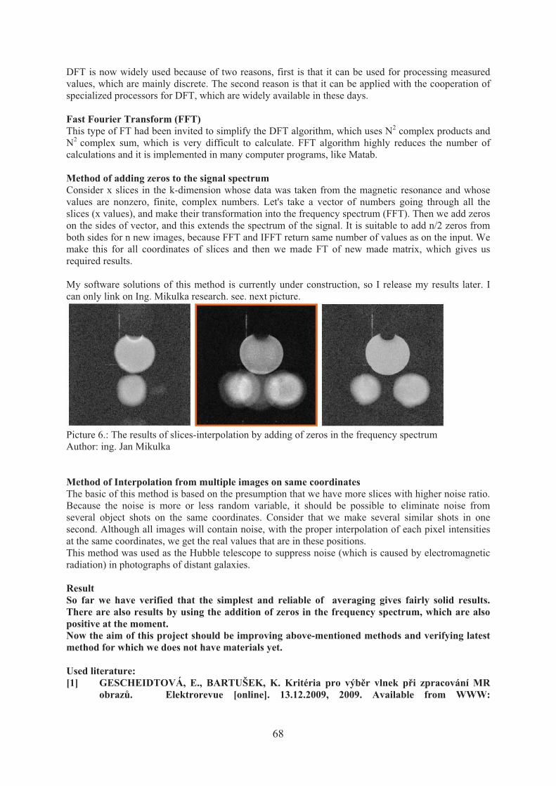
68
DFT is now widely used because of two reasons, first is that it can be used for processing measured values, which are mainly discrete. The second reason is that it can be applied with the cooperation of specialized processors for DFT, which are widely available in these days. Fast Fourier Transform (FFT) This type of FT had been invited to simplify the DFT algorithm, which uses N2 complex products and N2 complex sum, which is very difficult to calculate. FFT algorithm highly reduces the number of calculations and it is implemented in many computer programs, like Matab. Method of adding zeros to the signal spectrum Consider x slices in the k-dimension whose data was taken from the magnetic resonance and whose values are nonzero, finite, complex numbers. Let's take a vector of numbers going through all the slices (x values), and make their transformation into the frequency spectrum (FFT). Then we add zeros on the sides of vector, and this extends the spectrum of the signal. It is suitable to add n/2 zeros from both sides for n new images, because FFT and IFFT return same number of values as on the input. We make this for all coordinates of slices and then we made FT of new made matrix, which gives us required results. My software solutions of this method is currently under construction, so I release my results later. I can only link on Ing. Mikulka research. see. next picture.
Picture 6.: The results of slices-interpolation by adding of zeros in the frequency spectrum Author: ing. Jan Mikulka Method of Interpolation from multiple images on same coordinates The basic of this method is based on the presumption that we have more slices with higher noise ratio. Because the noise is more or less random variable, it should be possible to eliminate noise from several object shots on the same coordinates. Consider that we make several similar shots in one second. Although all images will contain noise, with the proper interpolation of each pixel intensities at the same coordinates, we get the real values that are in these positions. This method was used as the Hubble telescope to suppress noise (which is caused by electromagnetic radiation) in photographs of distant galaxies. Result So far we have verified that the simplest and reliable of averaging gives fairly solid results. There are also results by using the addition of zeros in the frequency spectrum, which are also positive at the moment. Now the aim of this project should be improving above-mentioned methods and verifying latest method for which we does not have materials yet. Used literature: [1] GESCHEIDTOVÁ, E., BARTUŠEK, K. Kritéria pro výb�r vlnek p�i zpracování MR
obraz�. Elektrorevue [online]. 13.12.2009, 2009. Available from WWW:

69
<http://elektrorevue.cz/cz/clanky/zpracovanisignalu/0/kriteria-pro-vyber-vlnek-pri- zpracovanimr-obrazu/>. ISSN 1213-1539.
[2] Fourierova transformace [online]. Available from WWW: <http://cs.wikipedia.org/wiki/Fourierova_transformace>. [3] MIKULKA, J. INTERPOLACE TROJROZMRNÝCH DAT MAGNETICKÉ REZONANCE. Elektrorevue [online]. 20.06.2011, 2011. Available from: < http://www.elektrorevue.cz/cz/clanky/ostatni-1/10/interpolace-trojrozmernych-dat- magneticke-rezonance-1/>
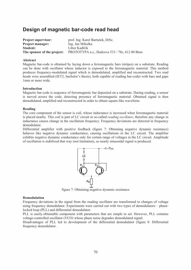
70
Design of magnetic bar-code read head Project supervisor: prof. Ing. Karel Bartušek, DrSc. Project manager: Ing. Jan Mikulka Student: Libor Kadl�ík The sponsor of the project: PROTOTYPA a.s., Hudcova 533 / 78c, 612 00 Brno Abstract Magnetic bar-code is obtained by laying down a ferromagnetic bars (stripes) on a substrate. Reading can be done with oscillator whose inductor is exposed to the ferromagnetic material. This method produces frequency-modulated signal which is demodulated, amplified and reconstructed. Two read heads were assembled (IET2, bachelor’s thesis), both capable of reading bar-codes with bars and gaps 1mm or more wide. Introduction Magnetic bar-code is sequence of ferromagnetic bar deposited on a substrate. During reading, a sensor is moved across the code, detecting presence of ferromagnetic material. Obtained signal is then demodulated, amplified and reconstructed in order to obtain square-like waveform. Reading The core component of the sensor is coil, whose inductance is increased when ferromagnetic material is placed nearby. This coil is part of LC circuit in so-called reading oscillator, therefore any change in inductance causes change in the oscillation frequency. Frequency deviations are detected in frequency demodulator. Differential amplifier with positive feedback (figure 7: Obtaining negative dynamic resistance) behaves like negative dynamic conductance, causing oscillations in the LC circuit. The amplifier exhibits negative dynamic conductance only for certain range of voltages in the LC circuit. Amplitude of oscillation is stabilized that way (not limitation), so nearly sinusoidal signal is produced.
figure 7: Obtaining negative dynamic resistance
Demodulation Frequency deviations in the signal from the reading oscillator are transformed to changes of voltage using frequency demodulator. Experiments were carried out with two types of demodulators – phase-locked loop (PLL) and differential demodulator. PLL is easily-obtainable component with parameters that are simple to set. However, PLL contains voltage-controlled oscillator (VCO) whose phase noise degrades demodulated signal. Disadvantages of PLL led to development of the differential demodulator (figure 8: Differential frequency demodulator.

71
figure 8: Differential frequency demodulator
Input signal Uin is split into branch containing bad-pass filter and branch containing inverting unity-gain amplifier. Upon summing signals from those branches, destructive interference occurs with intensity given by difference between input frequency fin and center frequency of the band-pass filter. Demodulation can be finished by simple rectifier. The differential demodulator exhibits low noise. On the other hand, input signal must be sinusoidal (or transfer characteristic is deformed), reading oscillator satisfies that. Amplification Usable component (read bar-code) in the demodulated signal is amplified. DC (less than 1Hz) and RF (more than 200Hz) components are suppressed. Reconstruction Read head produces PSF (point-spread function) if infinitively narrow ferromagnetic bar is read. Our read head has Gaussian PSF, because sensitivity of the sensor is not concentrated into single point in space. The read head produces signal given by convolution of bar-code (square waveform) with PSF. This convolution distortion makes edges of the signal round and attenuates its dense features.
figure 9: Detection of inflection point
Convolution distortion is removed by reconstruction – detection of inflection point in our case (figure 9: Detection of inflection point). Derivative of the distorted signal consists of many replicas of PSF. Sign of each replica determines polarity of bar-code edge (rising vs. falling), its location is denoted by peak of the replica (where second derivative of the distorted signal crosses zero). In order to mitigate false edge detection due to noise, edge should be ignored if absolute value of the first derivative is below given threshold. Results A prototype was build as part of the project [1] of IET2. Sensor featured Colpitts oscillator with coil wound on ferromagnetic core with diameter of 2mm. Frequency of oscillaton is 320kHz, lowered by 100 Hz in presence of ferromagnetic bar. Demodulation (PLL) and amplification produces signal on figure 10: Output signal of the prototype (IET2) (local minima corresponds to bars, maxima to gaps).
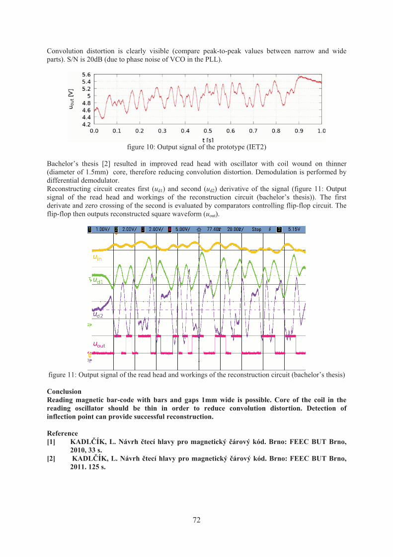
72
Convolution distortion is clearly visible (compare peak-to-peak values between narrow and wide parts). S/N is 20dB (due to phase noise of VCO in the PLL).
figure 10: Output signal of the prototype (IET2)
Bachelor’s thesis [2] resulted in improved read head with oscillator with coil wound on thinner (diameter of 1.5mm) core, therefore reducing convolution distortion. Demodulation is performed by differential demodulator. Reconstructing circuit creates first (ud1) and second (ud2) derivative of the signal (figure 11: Output signal of the read head and workings of the reconstruction circuit (bachelor’s thesis)). The first derivate and zero crossing of the second is evaluated by comparators controlling flip-flop circuit. The flip-flop then outputs reconstructed square waveform (uout).
figure 11: Output signal of the read head and workings of the reconstruction circuit (bachelor’s thesis) Conclusion Reading magnetic bar-code with bars and gaps 1mm wide is possible. Core of the coil in the reading oscillator should be thin in order to reduce convolution distortion. Detection of inflection point can provide successful reconstruction. Reference [1] KADL�ÍK, L. Návrh �tecí hlavy pro magnetický �árový kód. Brno: FEEC BUT Brno,
2010, 33 s. [2] KADL�ÍK, L. Návrh �tecí hlavy pro magnetický �árový kód. Brno: FEEC BUT Brno,
2011. 125 s.

73
NUMERICAL MODELING OF MAGNETIC SUSCEPTIBILITY ON MR IMAGES Project supervizor: prof. Ing. Karel Bartušek, DrSc, [email protected] Project leader: Ing. Jan Mikulka, [email protected] Project consultant: Michal Král , [email protected] Student: Zden�k Mžourek, [email protected] Project submitter: PROTOTYPA a.s., Hudcova 533 / 78c, 612 00 Brno Project specification: Design a method for correcting artifacts in MR images of magnetic susceptibility due to eddy currents of measured sample. Design and build a complex sample with a combination of positive and negative permeability for measurement in magnetic resonance tomograph and compare the measured magnetic field distribution images with the simulation resuts for the selected configuration. Process measured MR images of the proposed method and compare the corrected image with the original. Determine the magnetic susceptibility of measured sample. INTRODUCTION Nuclear magnetic resonance (NMR) is a well known non-invasive and non-destructive method that is used for determining material properties. The measured sample is in a strong magnetic field and depending on its homogeneity is based the quality of the resulting MR images. There are two basic methods of measuring MR. Spin-echo method is based on the excitation of nuclei by using two RF pulses and the subsequent detection of signal intensity at time TE (in this time of the magnetization vectors are in phase and the signal has a maximum size). This method compensates the magnetic field inhomogeneity. Gradient echo method works on a different principle. Nuclei are excited, while applying a magnetic field gradient, which causes a faster dephasing of magnetization vectors. When reading the signal, the phase matching is realized by magnetic field gradient of opposite polarity. Using this method does not compensate magnetic field inhomogeneity and therefore potential formation of artifacts that degrade the resulting MR image is possible. The magnetic field inhomogeneity can arise for example due to local changes in susceptibility (measured sample is made of ferromagnetic or paramagnetic material) or in the sample are induced eddy currents (the sample is conductive material), which counteract the magnetic field that is generated, and so this distort the magnetic field. Next, we will discuss the draft correction method for images measured using thegradient echo. SOLUTION The design will be based on the formula
(1) where TE is the time when there is a phasing of magnetization vectors, and T2
* is the effective relaxation time. The aim of the correction methods is to balance the phase image and remove artifactsin the image. This is achieved by multiplying the formula with the same exponencial member but with opposite sign.
(2) To this formula we substitute the following
(3)
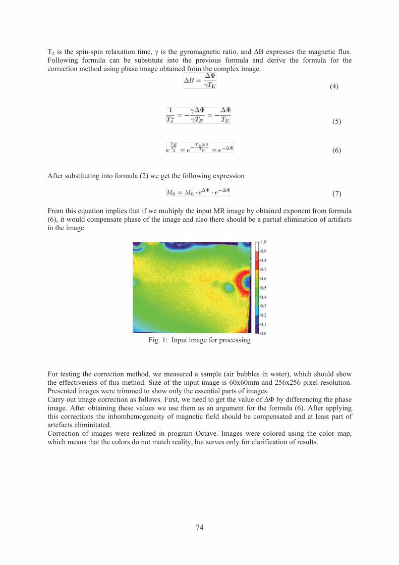
74
T2 is the spin-spin relaxation time, is the gyromagnetic ratio, and B expresses the magnetic flux. Following formula can be substitute into the previous formula and derive the formula for the correction method using phase image obtained from the complex image.
(4)
(5)
(6) After substituting into formula (2) we get the following expression
(7) From this equation implies that if we multiply the input MR image by obtained exponent from formula (6), it would compensate phase of the image and also there should be a partial elimination of artifacts in the image.
Fig. 1: Input image for processing
For testing the correction method, we measured a sample (air bubbles in water), which should show the effectiveness of this method. Size of the input image is 60x60mm and 256x256 pixel resolution. Presented images were trimmed to show only the essential parts of images. Carry out image correction as follows. First, we need to get the value of � by differencing the phase image. After obtaining these values we use them as an argument for the formula (6). After applying this corrections the inhomhemogeneity of magnetic field should be compensated and at least part of artefacts eliminitated. Correction of images were realized in program Octave. Images were colored using the color map, which means that the colors do not match reality, but serves only for clarification of results.

75
Fig. 2: Output image after processing.
CONCLUSION Based on the above formulas (1), (3), (4) we were able to derive the correction method for MR images. After applying the correction in program Octave, we have managed to at least compensate the phase of image, and therefore compensate magnetic field inhomogeneity. The elimination of artifacts that occur in an image wasn't succesful (blue areas in figure 2 should partialy diminish) . Since the artifacts are still present, so we will try to propose additional correction method, probably using convolution methods for filtering images. PREFERENCES [1] KUBÁSEK, R.; STEINBAUER, M.; BARTUŠEK, K. Material influences in MR
tomography, measurement and simulation. Journal of ELECTRICAL ENGENEERING. 2006, 57, s. 58-61. ISSN 1335-3632.
[2] JAN, J. Medical Image Processing, Reconstruction and Restoration - Concepts and Methods. Boca Raton, FL, USA : CRC Press, Taylor and Francis Group, 2006. 760 s. ISBN 0-8247-5849-8.
[3] BARTUŠEK, K.; FIALA, P.; MIKULKA, J. Numerical Modeling of Magnetic Field Deformation as Related to Susceptibility Measured with an MR System. Radioengineering. 2008. 17(4). p. 113 - 118. ISSN 1210-2512. �

76
DESIGN OF WIRELESS SIGNAL TRANSMISION FROM THERMAL SENSORS Project supervisor: doc. Ing. Petr Drexler, Ph.D. [email protected] Project leader: Ing. Zden�k Roubal [email protected] doc. Ing. Petr Ko�as, Ph.D. [email protected] Project consultant: Ing. Radek Javora, Ph.D. [email protected] Ing. Pavel Vá�o [email protected] Students: Martin Loviška [email protected] Tomáš Minár [email protected] Project submitter: ABB Ltd., Víde�ská 117, 619 00 Brno Project submission: Specify points in switchgear power compartments where it is needed to monitor temperature to avoid fault conditions due to overheating. Design reliable wireless data transmission from suitable temperature sensors and evaluation of received data. Realization of prototype sample and its subsequent testing in the temperature rise test. INTRODUCTION Voltage switchgear is one of the most important segments, which belongs to power distribution grid. The example of all-round switchgear with modular structure is shown in picture 1. It is a worldwide spread switchgear used for example in industry, power plants, marine and transport. This switchgear consists of compartments which are segregated by metal partitions and the live parts are air-insulated.
Img.1: switchgears
From a safety point of view switchgear´s internal functional units are designed and tested to be arc proof caused by short-circuit current. Short-circuit may be caused by various factors and our aim is to focus on the overheating of contact surfaces. The most common reasons of overheating is untightened screws in bus bar connections. With continuous monitoring of surface temperature changes we can prevent increased losses and possible damage to the switchgear. Such monitoring is needed in high-risk operations (mines, etc.) or with increased demands for reliability and operational safety (e.g. increased vibration rate at ferries etc.). Current solution for the issue utilizes IR sensors or infrared thermometers measuring through IR windows located on the walls of switchgear. The disadvantages of IR sensors are: impossibility of temperature monitoring on inaccessible places, sensors’ measuring might be affected by dust or surface contamination, metal compartments and wall structure changes needed, higher financial costs. In the case of infrared thermometers the measurement is not continuous and the line of sight and the access of personell is needed. The goal of the project is to find financially acceptable solution for long term temperature monitoring that could also be used in commercial solutions.
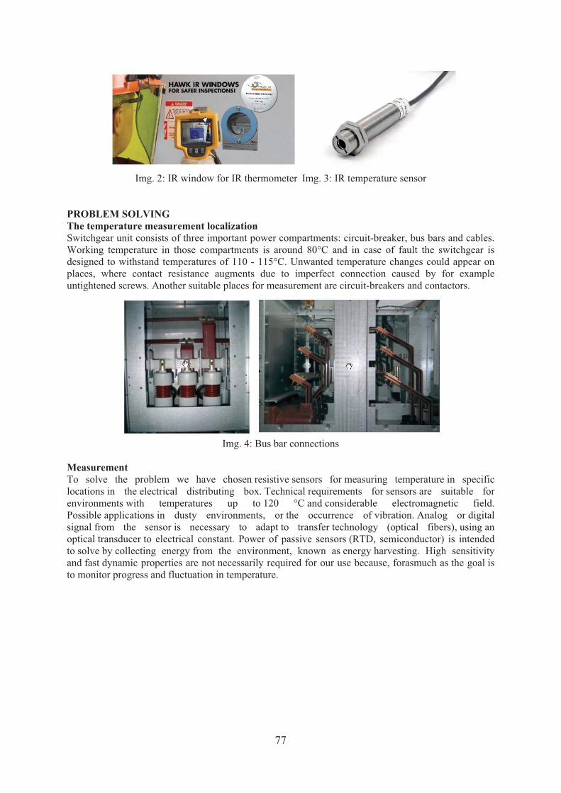
77
Img. 2: IR window for IR thermometer Img. 3: IR temperature sensor
PROBLEM SOLVING The temperature measurement localization Switchgear unit consists of three important power compartments: circuit-breaker, bus bars and cables. Working temperature in those compartments is around 80°C and in case of fault the switchgear is designed to withstand temperatures of 110 - 115°C. Unwanted temperature changes could appear on places, where contact resistance augments due to imperfect connection caused by for example untightened screws. Another suitable places for measurement are circuit-breakers and contactors.
Img. 4: Bus bar connections
Measurement To solve the problem we have chosen resistive sensors for measuring temperature in specific locations in the electrical distributing box. Technical requirements for sensors are suitable for environments with temperatures up to 120 °C and considerable electromagnetic field. Possible applications in dusty environments, or the occurrence of vibration. Analog or digital signal from the sensor is necessary to adapt to transfer technology (optical fibers), using an optical transducer to electrical constant. Power of passive sensors (RTD, semiconductor) is intended to solve by collecting energy from the environment, known as energy harvesting. High sensitivity and fast dynamic properties are not necessarily required for our use because, forasmuch as the goal is to monitor progress and fluctuation in temperature.
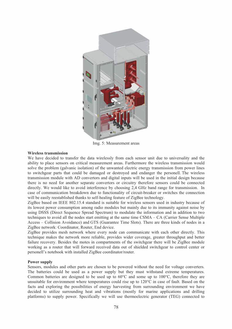
78
Img. 5: Measurement areas
Wireless transmission We have decided to transfer the data wirelessly from each sensor unit due to universality and the ability to place sensors on critical measurement areas. Furthermore the wireless transmission would solve the problem (galvanic isolation) of the unwanted electric energy transmission from power lines to switchgear parts that could be damaged or destroyed and endanger the personell. The wireless transmission module with AD convertors and digital inputs will be used in the initial design because there is no need for another separate convertors or circuitry therefore sensors could be connected directly. We would like to avoid interference by choosing 2,4 GHz band range for transmission. In case of communication breakdown due to functionality of circuit-breaker or switches the connection will be easily reestablished thanks to self-healing feature of ZigBee technology. ZigBee based on IEEE 802.15.4 standard is suitable for wireless sensors used in industry because of its lowest power consumption among radio modules but mainly due to its immunity against noise by using DSSS (Direct Sequence Spread Spectrum) to modulate the information and in addition to two techniques to avoid all the nodes start emitting at the same time CSMA – CA (Carrier Sense Multiple Access – Collision Avoidance) and GTS (Guarantee Time Slots). There are three kinds of nodes in a ZigBee network: Coordinator, Router, End device. ZigBee provides mesh network where every node can communicate with each other directly. This technique makes the network more reliable, provides wider coverage, greater throughput and better failure recovery. Besides the motes in compartments of the switchgear there will be ZigBee module working as a router that will forward received data out of shielded switchgear to control center or personell’s notebook with installed ZigBee coordinator/router. Power supply Sensors, modules and other parts are chosen to be powered without the need for voltage converters. The batteries could be used as a power supply but they must withstand extreme temperatures. Common batteries are designed to be used up to 60°C and some up to 100°C, therefore they are unsuitable for environment where temperatures could rise up to 120°C in case of fault. Based on the facts and exploring the possibilities of energy harvesting from surrounding environment we have decided to utilize surrounding heat and vibrations (mostly for marine applications and drilling platforms) to supply power. Specifically we will use thermoelectric generator (TEG) connected to

79
power management integrated circuit, which could be supplemented by piezoelectric element to harvest energy from vibrations. The device will work without exchanging battery. CONCLUSIONS Wireless sensors powered by energy harvesting module could improve productivity and device protection in industry. Fault due to an internal arc could be avoided by continuous monitoring of several switchgear parts. What’s more we would like to extend our device by optical fiber sensors to measure current and temperature too. Owing to insufficient resistance of commercial modules to extreme conditions we would like to construct our own wireless module that could be simply extensible by another sensors thus the device could become essential structure part of universal wireless sensor networks. REFERENCES [1] RIPKA, Pavel, et al. Senzory a p�evodníky. Praha : Vydavatelství �VUT, 2005. 129 s. ISBN
80-01-03123-3 [2] WANZHI, Qiu; PENG, Hao; EVANS, R.J. An efficient self-healing process for ZigBee
sensor networks. In International Symposium on Communications and Information Technologies (ISCIT 2007) [online]. Sydney,. NSW : [s.n.], 19 Oct. 2007, 04 December 2007 [cit. 2011-06-23]. Dostupné z WWW: <http://ieeexplore.ieee.org/stamp/stamp.jsp?tp=&arnumber=4392233>. ISBN 978-1-4244-0976-1, doi:10.1109/ISCIT.2007.4392233.
[3] GUNGOR, V.C.; HANCKE, G.P. Industrial Wireless Sensor Networks: Challenges, Design Principles, and Technical Approaches. IEEE Transactions on Industrial Electronics [online]. Oct. 2009, vol. 56, no. 10, [cit. 2011-06-23]. Dostupné z WWW: <http://ieeexplore.ieee.org/stamp/stamp.jsp?tp=&arnumber=4796311>. ISSN 0278-0046.
[4] GASCÓN, David. Wireless sensor networks [online]. November 17, 2008 [cit. 2011-06-23]. 802.15.4 vs ZigBee. Dostupné z WWW: <http://www.sensor-networks.org/index.php?page=0823123150>.
[5] Electronics Bus [online]. c2011 [cit. 2011-06-23]. Thermoelectric Energy Harvesting – Thermoelectric Sensors & Transducers. Dostupné z WWW: <http://electronicsbus.com/thermoelectricity-energy-harvesting-thermoelectric-sensors-transducers/>.
[6] DALOLA, S., et al. Autonomous Sensor System with RF Link and Thermoelectric Generator for Power Harvesting. In I2MTC 2008 - IEEE International Instrumentation and Measurement Technology Conference [online]. Victoria, BC, Canada : [s.n.], May 2008 [cit. 2011-06-23]. Dostupné z WWW: <http://ieeexplore.ieee.org/stamp/stamp.jsp?tp=&arnumber=4547257>. ISBN 978-1-4244-1540-3, ISSN 1091-5281, doi:10.1109/IMTC.2008.4546980 .

80
THE CONSTRUCTION AND DESIGN A TRANSFORMER Project supervisor: doc. Ing. Petr Drexler, Ph.D., [email protected] Project leader: Ing. Zden�k Roubal, [email protected] Project consultants: Ing. Radek Javora, Ph.D., [email protected]
Ing. Pavel Vá�o, [email protected] Students: Vít Smejkal, [email protected] Project submitter: ABB Ltd., Víde�ská 117, 619 00 Brno Project submission: Acquaint with the calculation algorithm of power supply transformers. Implement this algorithm to the Matlab environment. Further acquaint with parameters needed for measuring current transformers design. INTRODUCTION The ideal power supply transformer has no losses and the secondary voltage is independent on the connected burden. The transformer is warmed up and the design is limited by the maximal permissible temperature, because of losses in magnetic circuit and windings. It is economy to find the minimal dimension of core and wires to minimize the production price, but in some cases it is required to design the transformer with maximal efficiency (not the smallest core).
corebobbinwire
Fig. 7: Transformer with EI core - horizontal section
Current transformer is used to reduce a measured current to the value that can be indicated by the measuring devices and also isolates this device from the primary circuit. Requirement is to transform the current with minimal error in a working range of currents and to limit the maximal secondary current to protect connected instruments. PROBLEM SOLVING The design of power supply transformers with EI core is usually based on choosing parameters (flux density, current density, etc.) according to transformed power. One of the requirements was not to use this values from tables given in literature ([1]), but to calculate the maximal values for optimal working. For example the flux density in a magnetic circuit is limited by the maximal losses in a core, the magnetizing current and the saturation of a magnetic circuit. The current density J is calculated by the formula (1), derived from the formula for losses in a one coil:
Cu12
Cu_maxCu
��10�
mP
J
� [A/mm2; kg/m3, W, ��m, kg], (1)
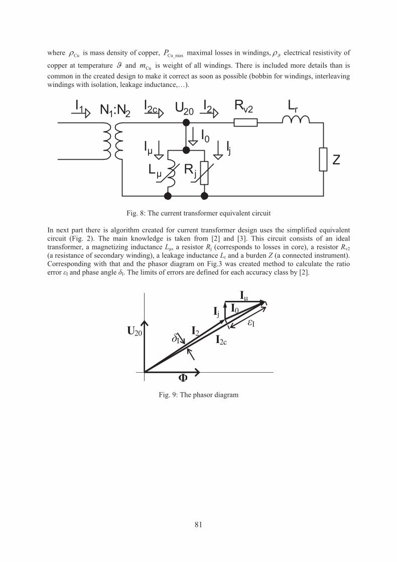
81
where Cu is mass density of copper, Cu_maxP maximal losses in windings, electrical resistivity of
copper at temperature and Cum is weight of all windings. There is included more details than is common in the created design to make it correct as soon as possible (bobbin for windings, interleaving windings with isolation, leakage inductance,…).
R
ZR L
L I
I I
N :N 1 I 2c I 2 v2 r
μ j
j μ
U 20
I 0
1 2
Fig. 8: The current transformer equivalent circuit In next part there is algorithm created for current transformer design uses the simplified equivalent circuit (Fig. 2). The main knowledge is taken from [2] and [3]. This circuit consists of an ideal transformer, a magnetizing inductance L�, a resistor Rj (corresponds to losses in core), a resistor Rv2 (a resistance of secondary winding), a leakage inductance Lr and a burden Z (a connected instrument). Corresponding with that and the phasor diagram on Fig.3 was created method to calculate the ratio error �I and phase angle �I. The limits of errors are defined for each accuracy class by [2].
U20 I2c I2
I�
Ij
�I
�I
I0
�
Fig. 9: The phasor diagram

82
Fig. 10: Program for design power supply transformer (left) and current transformer (right) The algorithms were implemented to the Matlab environment. There were created also graphics user interfaces for comfortable entering the input data. The previews are on the Fig. 4. Material characteristics and databases of wires and cores‘ dimensions are loaded from Excel sheets. The design is automatized and user can choose optimalization for the required solution. CONCLUSIONS In this project were described designs of power supply transformer with EI core and current transformer and two programs in Matlab were created for their designing. Both programs were verified by measuring transformers that were designed. The difference between the design and measurement of transformer is caused for power supply transformers by choosing grain oriented steel for magnetic circuit. Accuracy of design current transformers corresponds to dissipation of core producing. REFERENCES [1] FAKTOR, Zden�k. Transformátory a cívky. 1. vydání. Praha : BEN - technická
literatura, 1999. 393 s. ISBN 80-86056-49-X, EAN: 9788086056494. [2] �SN EN 60044-1. P�ístrojové transformátory - �ást 1: Transformátory proudu. Praha :
�eský normaliza�ní institut, 2001. 44 s. [3] KOPE�EK, Jan; DVO�ÁK, Miloš. P�ístrojové transformátory : m��icí a jisticí. 1.
vydání. Praha : Academica, 1966. 492 s.

83
Measuring box with Peltier cells Project supervisor: Ing. Petr Drexler, Ph.D., [email protected] Project leader: Ing. Tomáš K�íž, [email protected] Ing. Zden�k Roubal, [email protected] Project consultant: Ing. Tibor Bachorec, Ph.D. [email protected] Students: Pavel Vejnar [email protected] Project submitter: SVS FEM Ltd., Škrochova 3886/42, 61500 Brno-Židenice Project submitter: Learn the basic properties of Peltier cells. Find different ways of cooling the hot side. Apply this knowledge to reduce noise and input quiescent current of operational amplifier. Solve the problem of condensation of moisture in a special Electrometric amplifier, which will use the Peltier cells. Consult the results. Make modeling thermal conditions Peltier cells in ANSYS. INTRODUCTION Quest has been modify and fix for particular product. Creating container, cooled by Peltier cells. In the container there are continuous temperature control. The size of the chamber is at least 200x200x200 mm, due to measure toroidal transformer. Peltier cell is based on the Peltier effect. Discovered by C. J. Peltier in 1834. This component consists of two metals, usually bismuth and tellurium. When a voltage is applied to it, it creates a temperature difference. At the atomic scale, an applied temperature gradient causes charged carriers in the material to diffuse from the hot side to the cold side. Their disadvantage is the high power consumption and large production of heat that must be removed.
Pic.1: Peltier cells. A Peltier cells creates a voltage when there is a different temperature on each side. PROBLEM SOLVING Design of facility is divided into two parts. The first is the container in which to place the component and Peltier cells with cooler for water cooling. The second part is cooler for water from Peltier cells.
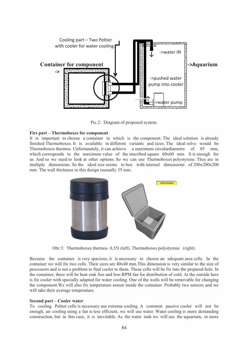
84
Pic.2: Diagram of proposed system.
. Firs part – Thermoboxes for component It is important to choose a container in which is the component. The ideal solution is already finished Thermoboxes. It is available in different variants and sizes. The ideal solve would be Thermoboxes thermos. Unfortunately, it can achieve a maximum circulardiameter of 85 mm, which corresponds to the maximum value of the inscribed square 60x60 mm. It is enough for us. And so we need to look at other options. So we can use Thermoboxes polystyrene. They are in multiple dimensions. So the ideal size seems to box with internal dimensions of 200x200x200 mm. The wall thickness in this design isusually 35 mm.
Obr.3: Thermoboxes thermos. 0,35l (left), Thermoboxes polystyrene. (right). Because the container is very spacious, it is necessary to choose an adequate area cells. In the container we will fix two cells. Their sizes are 40x40 mm.This dimension is very similar to the size of processors and is not a problem to find cooler to them. These cells will be fix into the prepared hole. In the container, there will be heat sink fins and low-RPM fan for distribution of cold. At the outside here is fix cooler with specially adapted for water cooling. One of the walls will be removable for changing the component.We will also fix temperature sensor inside the container. Probably two sensors and we will take their average temperature. Second part – Cooler water To cooling Peltier cells is necessary use extreme cooling. A common passive cooler will not be enough, air cooling using a fan is less efficient, we will use water. Water cooling is more demanding construction, but in this case, it is inevitable. As the water tank we will use the aquarium, or more
����Cooling�part�–�Two�Peltier� � � � � � � �� � with�cooler�for�water�cooling. �>water�IN Container for component� � � � � � �>Aquarium���� �>� � � � � � � � � � �� � � � � �>pushed�water�� � �� � � � � � � � pump�into�cooler � � � � � � � � � � � � � � � � � � � �� � � � � � � � ����������>water�pump� � �� � � � � � � � � ���� � � �� � � � � � � �

85
ideal would be a radiator for better cooling water during operation. The liquid will circulate through the cooling blocks placed on the Peltier cells using the water pump. The liquid still be able to cool just to room temperature. We can use ice which lowers its temperature and reduce the temperature in the container. CONCLUSIONS We moved only in theory for now and hard work on the design and subsequent implementation of that solution. Practical results may differ from expected. Our goal is to reach a temperature of -30 ° C to +40 ° C. The temperature container will be simulated in ANSYS. REFERENCES [1] AKSENOV, A. I. – GLUŠKOVA, D. N. – IVANOV, V. I.: Chlazení polovodi�ových
sou�ástek. Praha, SNTL 1975. s. 61-66. [2] KUBINA, Pavel. Regulace teploty pomocí Peltierových termoelektrických modul� [online].
2011 [cit. 2011-06-27]. Dostupný z WWW: <http://www.odbornecasopisy.cz/index.php?id_document=30765>.

86
CONTROL SPECIAL AUTOMATS Project supervisor: Ing. Petr Drexler, Ph.D. ([email protected]) Project leader: Ing. Zden�k Roubal ([email protected]) Ing. Michal Hadinec ([email protected]) Project consultant: Michal Král ([email protected]) Students: Vilém Závodný ([email protected]) Project submitter: PROTOTYPA a.s., Hudcova 533 / 78c, 612 00 Brno Project submission: Programming microprocessors used in robotics. This project is aimed at designing a special electromechanical systems and their control. Programs are required in the shape and form of remote control. They will be applied for special applications or loaded in extremely risky environment. INTRODUCTION Based on a closer assignment, which consisted of a mechanical device using the motor control and position indication by means of sensors, I had to choose from several options. The first variant was to use a stepper motor. It is very accurate and powerful, but has a high consumption and especially the hard to measure its moment. Another option was to use a regular electromotor. Here it would be fairly easy to measure the torque, but its precise control would be a problem. The third idea was to use the servo motor, which is accurate, powerful and torque measurement would be possible. Finally, this idea has been tested and virtually created the module, which is described below. Even the fourth option and that use brushless motor, because it has excellent power and torque measurement could be simpler than the stepper motor.
Fig.1: Stepper motor, servo motor, brushless motor.
PROBLEM SOLVING In this section I will deal with it just servo motors and brushless motors, because the other two possible solutions not have been practically implemented. Servomotors In principle, the common servo motors that can be controlled by pulse frequency of 30 to 90 Hz and width of 0.5 to 2.5 ms (Fig. 3) due to the electronics inside the servo motor (Fig. 2). Another advantage of the gears that make the resulting force is much higher than for ordinary electromotor.
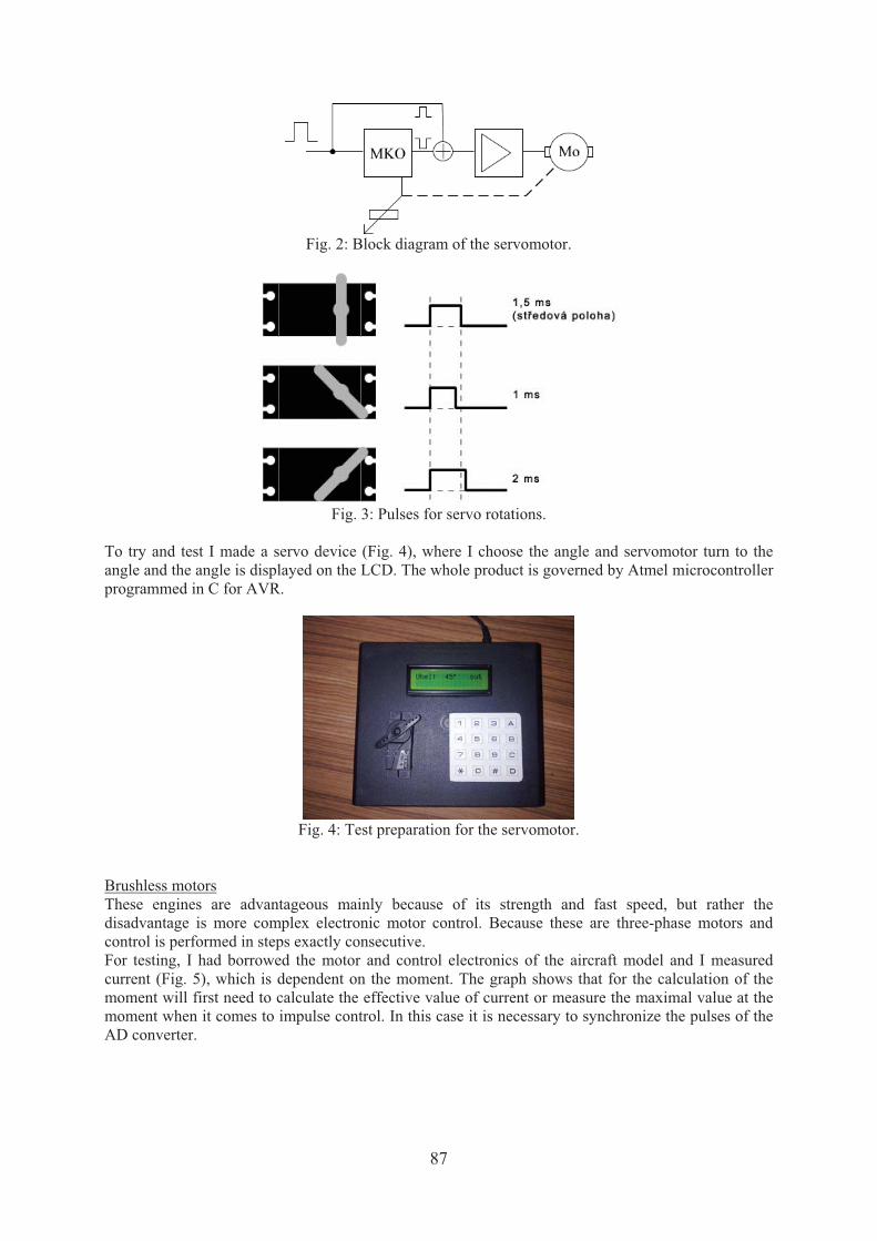
87
Fig. 2: Block diagram of the servomotor.
Fig. 3: Pulses for servo rotations.
To try and test I made a servo device (Fig. 4), where I choose the angle and servomotor turn to the angle and the angle is displayed on the LCD. The whole product is governed by Atmel microcontroller programmed in C for AVR.
Fig. 4: Test preparation for the servomotor.
Brushless motors These engines are advantageous mainly because of its strength and fast speed, but rather the disadvantage is more complex electronic motor control. Because these are three-phase motors and control is performed in steps exactly consecutive. For testing, I had borrowed the motor and control electronics of the aircraft model and I measured current (Fig. 5), which is dependent on the moment. The graph shows that for the calculation of the moment will first need to calculate the effective value of current or measure the maximal value at the moment when it comes to impulse control. In this case it is necessary to synchronize the pulses of the AD converter.
88
Fig. 5: Measured motor current when unloaded.
CONCLUSIONS So far I managed to test the actuator and determine that it is not entirely appropriate for our solution because it fails to respond sufficiently precise and demanding conditions. As has been previously inspected and is suitable stepper motor, but it is not possible to measure torque, hence it is impossible to know the load. I think that might be suitable brushless motor torque even if the count is probably pretty difficult thing. But I am convinced that computing power will be sufficient Atmel microcontroller. REFERENCES [1] VÁ�A, V. Atmel AVR programování v jazyce C. 1. vydání. Praha : BEN - technická
literatura, 2003. 216 s. ISBN 80-7300-102-0. [2] ROUBAL, Z; FRIEDL, M. Mikrokontroléry ATMEL AVR. Brno, 2009. 54 s.
89
Wireless remote control with a coded transmission Project supervisor: Ing. Petr Drexler, Ph.D. ([email protected]) Project leader: Ing. Zoltán Szabó ([email protected]) Ing. Michal Hadinec ([email protected]) Project consultant: Michal Král ([email protected]) Students: Libor Blažek, Roman Bracinik, Mat�j Polách Project submitter: PROTOTYPA a.s., Hudcova 533 / 78c, 612 00 Brno INTRODUCTION The project is focused to the controlling of two or more data receivers with pyrotechnical accessories. It will be used mainly for security purposes like fire fighting. The main requirement for functioning of the equipment is ability to send two or more signals subsequently by the main transmitter, the way the receivers can be started at the same time with the minimum time difference. Security is very important aspect; therefore, the transmitter has to be treated in order to prevent receiving different signal than was send by transmitter. This can be done by adding modules for coding and decoding. Constant communication between transmitter and receiver will be set for checking the starting signal sent to the all receivers. Proposal for organization. Control module: The transmitter will be convertible because the communication can flow both ways. The cut over between the modes will be done by the switch or by the configuration of jumpers. The price should be as low as possible, because while using the destruction of receiver is probable. The equipment should be whether resistible. The scheme shows the principle of circuit for controlling module. Every single part includes important function in connection. Therefore, it can include two or more circuits. The main role of controlling module is to check whether both distinct modules are in touch by the repeated checking of connection, and secure the subsequent activation of both distinct modules. In case one of the distinct modules is not in touch, the circuit must ensure the distant modules are not activated or they have to indicate this mistake by check light.
Fig. 1: Control module, repote module

90
RJ - Processor which drives the whole process. It generates the time evidence by which it is consequently coded in order to prevent unintentional activation of distant modules. Moreover, a special cycle for coding will be present. It will find out whether both distant modules are in touch and based on it make a decision whether it allow the starting of distant modules. HO – provides stable frequence which is necessary for generating of the time evidence. This frequence should be stable enough. The quality oscillator like connection with a crystal can be used. RF - This module should provide the connection between processor and distant modules. The aim is to reach the distance, without giving up an expenditure (the distant modules will be provided by batteries). NZ – power supply for better mobility. The equipment will be used mainly in interiers; therefore, battery supplying is more appropriate. Moreover, indicator of battery state will be very practical. Repote module RF Module There is a wide scale how the wireless transmission can be realized. It is not necessary to work on something which has already been invented and functioned. In every market with electronic items the modules can be bought. It is necessary to choose the appropriate module, examine and connect it. On the market there are modules with frequency 868 MHz a 2,4 GHz, radio, Bluetooth, WiFi, ZigBee... The information about coverage differ based on different sources and depends on several factors. They are in range from 10 to 100 meters. The best way is to test more modules and choose the most appropriate for the area. From the offer of Farnell (one of the biggest on the internet) I have chosen module from Microchip which has an interesting parameters and solid price.
MICROCHIP
MRF24J40MB-I/RM, RF, TRX, 2.4GHZ, +20DBM
• IEEE Std. 802.15.4™ Compliant RF Transceiver • Supports ZigBee®, MiWi™, MiWi P2P and Proprietary Wireless Networking Protocols • Small Size: 0.9" x 1.3" (22.9 mm x 33.0 mm), Surface Mountable Compatible with Microchip Microcontroller Families (PIC16F, PIC18F, PIC24F/H, dsPIC33 and PIC32) • Up to 4000 ft. Range • Operating Voltage: 2.4-3.6V (3.3V typical) • Temperature Range: -40°C to +85°C Industrial • Low-Current Consumption: - RX mode: 25 mA (typical) - TX mode: 130 mA (typical) - Sleep: 5 uA (typical)
• ISM Band 2.405-2.475 GHz Operation • Data Rate: 250 kbps • -102 dBm Typical Sensitivity with -23 dBm Maximum Input Level • +20 dBm Typical Output Power with 56 dB TX Power Control Range • Hardware CSMA-CA Mechanism, Automatic ACK Response and FCS Check • Independent Beacon, Transmit and GTS FIFO • Supports all CCA modes and RSS/LQI • Automatic Packet Retransmit Capable • Hardware Security Engine (AES-128) with CTR, CCM and CBC-MAC modes • PCB antena • cena: 330.71 CZK

91
Next step After solving the complete concept we draw a system and create the protocol which will be programmed to microcontrollers, including transmitted news, states, and activities. Consequently, the components will be bought and the prototypes will be made. The measurement and examining will be provided, and necessary changes will be made.
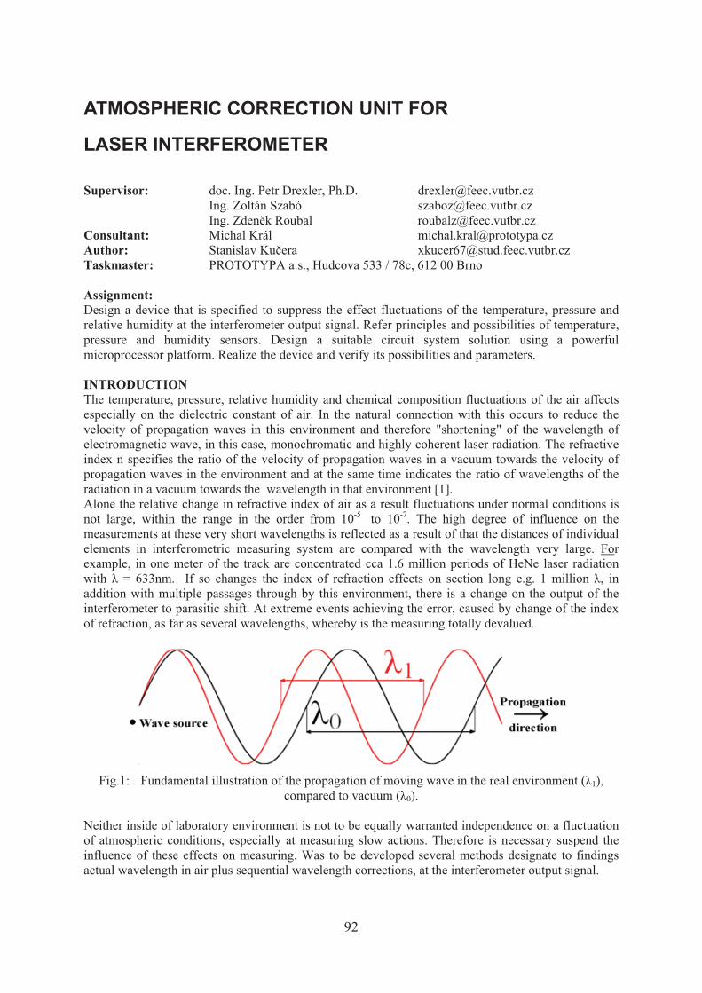
92
ATMOSPHERIC CORRECTION UNIT FOR
LASER INTERFEROMETER
Supervisor: doc. Ing. Petr Drexler, Ph.D. [email protected] Ing. Zoltán Szabó [email protected] Ing. Zden�k Roubal [email protected] Consultant: Michal Král [email protected] Author: Stanislav Ku�era [email protected] Taskmaster: PROTOTYPA a.s., Hudcova 533 / 78c, 612 00 Brno Assignment: Design a device that is specified to suppress the effect fluctuations of the temperature, pressure and relative humidity at the interferometer output signal. Refer principles and possibilities of temperature, pressure and humidity sensors. Design a suitable circuit system solution using a powerful microprocessor platform. Realize the device and verify its possibilities and parameters. INTRODUCTION The temperature, pressure, relative humidity and chemical composition fluctuations of the air affects especially on the dielectric constant of air. In the natural connection with this occurs to reduce the velocity of propagation waves in this environment and therefore "shortening" of the wavelength of electromagnetic wave, in this case, monochromatic and highly coherent laser radiation. The refractive index n specifies the ratio of the velocity of propagation waves in a vacuum towards the velocity of propagation waves in the environment and at the same time indicates the ratio of wavelengths of the radiation in a vacuum towards the wavelength in that environment [1]. Alone the relative change in refractive index of air as a result fluctuations under normal conditions is not large, within the range in the order from 10-5 to 10-7. The high degree of influence on the measurements at these very short wavelengths is reflected as a result of that the distances of individual elements in interferometric measuring system are compared with the wavelength very large. For example, in one meter of the track are concentrated cca 1.6 million periods of HeNe laser radiation with � = 633nm. If so changes the index of refraction effects on section long e.g. 1 million �, in addition with multiple passages through by this environment, there is a change on the output of the interferometer to parasitic shift. At extreme events achieving the error, caused by change of the index of refraction, as far as several wavelengths, whereby is the measuring totally devalued.
Fig.1: Fundamental illustration of the propagation of moving wave in the real environment (�1),
compared to vacuum (�0). Neither inside of laboratory environment is not to be equally warranted independence on a fluctuation of atmospheric conditions, especially at measuring slow actions. Therefore is necessary suspend the influence of these effects on measuring. Was to be developed several methods designate to findings actual wavelength in air plus sequential wavelength corrections, at the interferometer output signal.
93
Approximation of the influence of the main environmental parameters on the refractive index [2]:
Temperature:
Pressure:
Relative humidity:
CO2 content:
Fig. 2: Graphic illustration of changes the refractive index of air depending on variables temperature
and pressure, constant relative humidity 0 and 100%, for � = 633 nm (n = 1 + n). One of option is determination of the refractive index from calculation by Edlén’s equation. Edlén equation are empirical interactions for calculation the wavelength of light in air, were to be progressively several times updated. For revision from 1994 [3][4] is the uncertainty associated with these equations , for wavelengths � = 350 – 650nm, c. , the value comparable with wavelength
stability of HeNe laser LIMTEK LS10.1. At using these metod be for calculation measured these parameters: temperature, pressure, relative humidity and in some cases also content of CO2 in atmosphere. Formula includes the dispersive component and be true for air with normal chemical composition. The Edlén equation – revision 1994 [3][4]:
, (2)
, (3)

94
where (n-1)tp is refractive index at temperature t (°C), pressure p (Pa), (n-1)s is dispersive component for the wavenumber (�m-1). For air with nonzero humidity:
, (4) where f (Pa) is partial pressure of water vapour. Calculation of pressure water vapor from relative humidity RH (%) is complicated, e.g. [5]. Standard content of CO2 in air is 450 ppm, correction equation:
, (5) where x determine CO2 part by volume (-). SPECIFICATIONS Air parameters sensors: Demands on range and accuracy of sensors particular parameters were to be defined with reference to results of Edlén equation, complication of use and availability. Absolute accuracy of measurement temperature within the range 0 - 40 °C: ± 0,1 °C Absolute accuracy of measurement pressure within the range 75 - 110 kPa: ± 0.1 kPa Absolute accuracy of measurement relative humidity within the range 0 - 95 %: ± 2 % Calculation for at least positive dependence of limiting errors of sensors was given relative wavelength
error correction, in this range, as : (-), which is for use at interferometric measuring enough suitable value. Fundamental block diagram function of device:
CONCLUSION The specifications of designed instrument were to be given in so far, with a view to could compete commercially manufactured instruments also though, that the these system is in large measure matched to concrete laboratory application. Grand influence on required performance of the computing system has required maximum treatable skip speed of measured object and from that resulting the maximum frequency of both interferential signals (sin and cos).

95
Modification plus preprocessing of these signals is implemented in programmable gate array and be in progress in real time. E.g. for skip speed 1 m.s-1 must be system able to process digital signal about frequency minimally c. 13 MHz. The part of device, that including air parameters sensors and actual wavelength calculation is already successfully designed. At the present time is in progress development parts of the HW and algorithms of processing interferential signals. REFERENCES WEBB, Collin E; JONES, Julian D C . Handbook of Laser Technology and Applications : Volume I: Principles. London: Institute of Physics Publishing, 2004. 301 p. ISBN 0-7503-0960-1. WEBB, Collin E; JONES, Julian D C . Handbook of Laser Technology and Applications : Volume III: Application. London : Institute of Physics Publishing, 2004. 1166 p. ISBN 0-7503-0963-6. BIRCH, K.P.; DOWNS, M.J. An updated Edlen equation for the refractive index of air. Metrologia. 1993, 30, p. 155-162. BIRCH, K.P.; DOWNS, M.J. Correction to the updated Edlen equation for the refractive index of air. Metrologia. 1994, 31, p. 315-316. STONE, Jack A.; ZIMMERMAN, Jay H. National Institute of Standards and Technology : Engineering Metrology Toolbox [online]. 2001, last updated 23th september 2010 [cit. 2011-06-16]. Index of Refraction of Air. Online from WWW: <http://emtoolbox.nist.gov/Wavelength/Documentation.asp>.
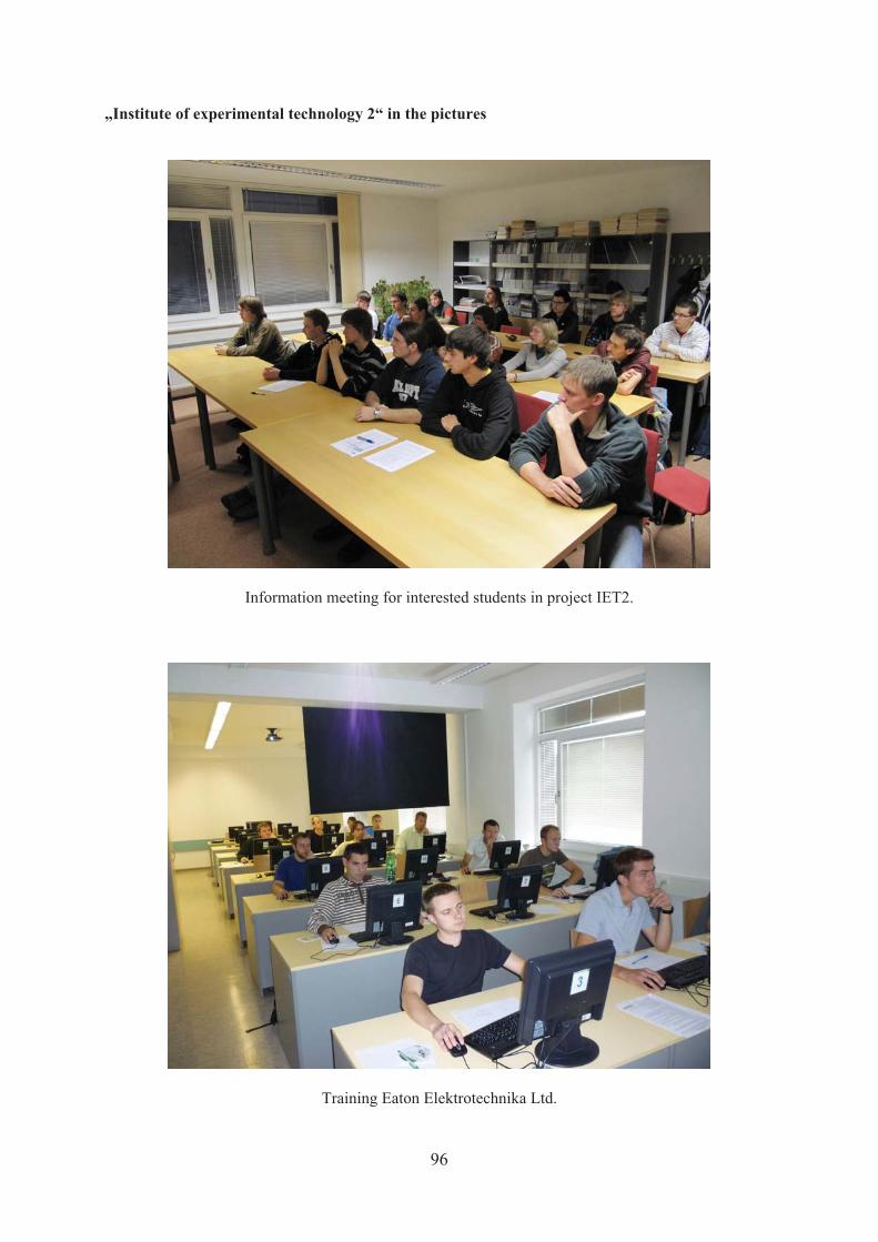
96
„Institute of experimental technology 2“ in the pictures
Information meeting for interested students in project IET2.
Training Eaton Elektrotechnika Ltd.
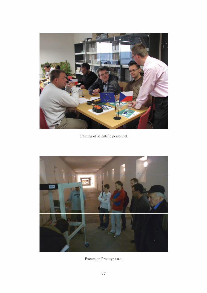
97
Training of scientific personnel.
Excursion Prototypa a.s.
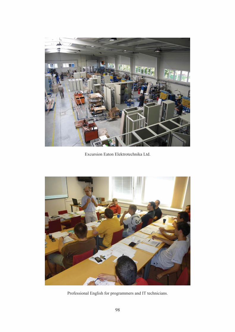
98
Excursion Eaton Elektrotechnika Ltd.
Professional English for programmers and IT technicians.
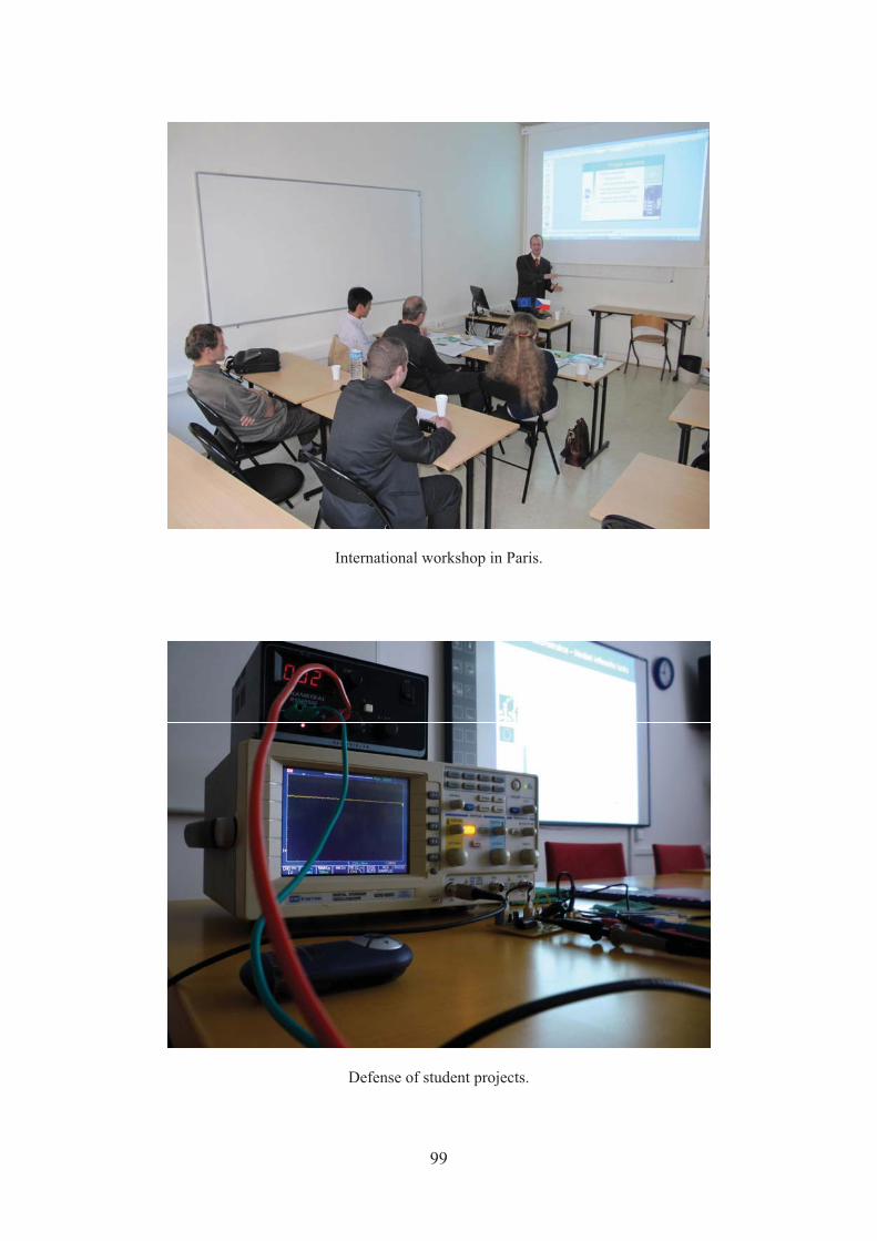
99
International workshop in Paris.
Defense of student projects.

100