Embed Size (px)
Citation preview
Confined Carriers
DRAGICA VASILESKAPROFESSOR
ARIZONA STATE UNIVERSITY
Outline
Nanoelectronics
Quantum Confined Structures: General Considerations
Quantum Wells Triangular: Si/SiO2 Interface Rectangular: Heterostructures
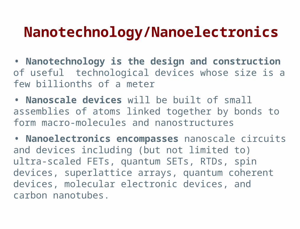
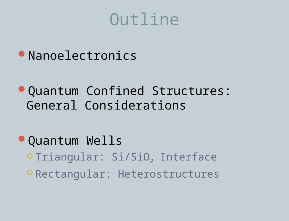
Nanotechnology/Nanoelectronics
• Nanotechnology is the design and construction of useful technological devices whose size is a few billionths of a meter
• Nanoscale devices will be built of small assemblies of atoms linked together by bonds to form macro-molecules and nanostructures
• Nanoelectronics encompasses nanoscale circuits and devices including (but not limited to) ultra-scaled FETs, quantum SETs, RTDs, spin devices, superlattice arrays, quantum coherent devices, molecular electronic devices, and carbon nanotubes.
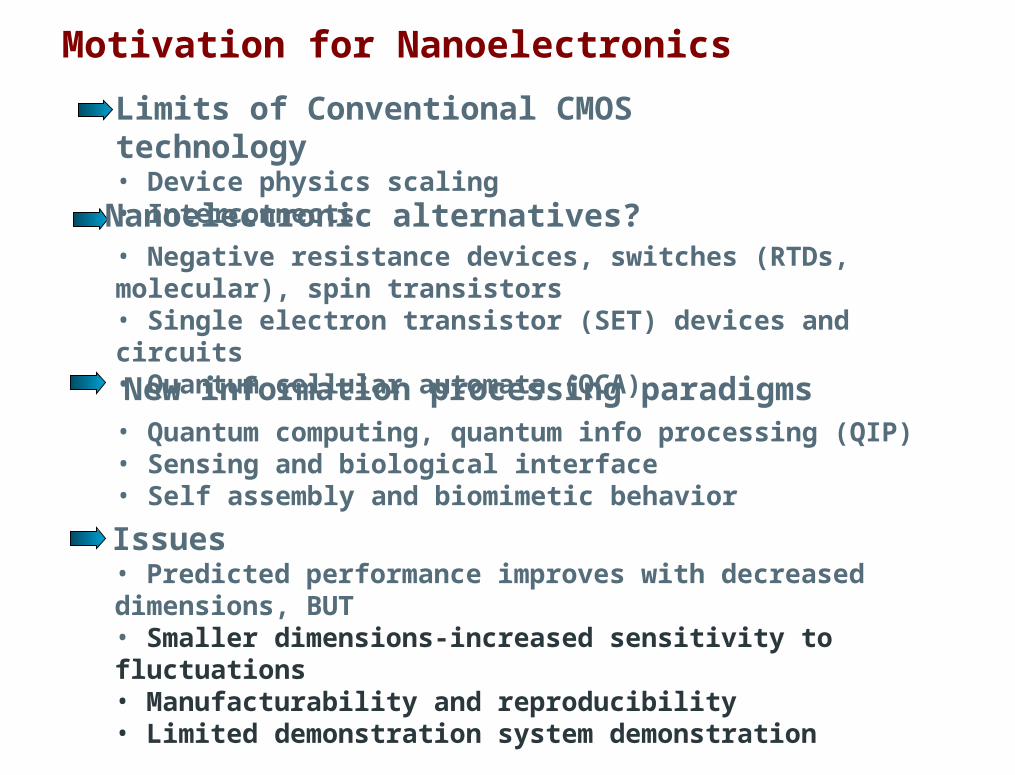
Motivation for Nanoelectronics
• Negative resistance devices, switches (RTDs, molecular), spin transistors• Single electron transistor (SET) devices and circuits• Quantum cellular automata (QCA)
Limits of Conventional CMOS technology• Device physics scaling • Interconnects Nanoelectronic alternatives?
Issues • Predicted performance improves with decreased dimensions, BUT• Smaller dimensions-increased sensitivity to fluctuations• Manufacturability and reproducibility• Limited demonstration system demonstration
New information processing paradigms• Quantum computing, quantum info processing (QIP)• Sensing and biological interface• Self assembly and biomimetic behavior
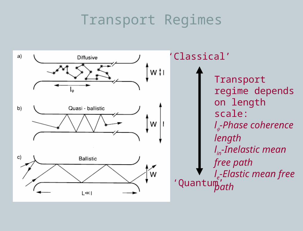
Transport Regimes
‘Classical’
‘Quantum’
Transport regime depends on length scale: l-Phase coherence lengthlin-Inelastic mean free pathle-Elastic mean free path
P
P
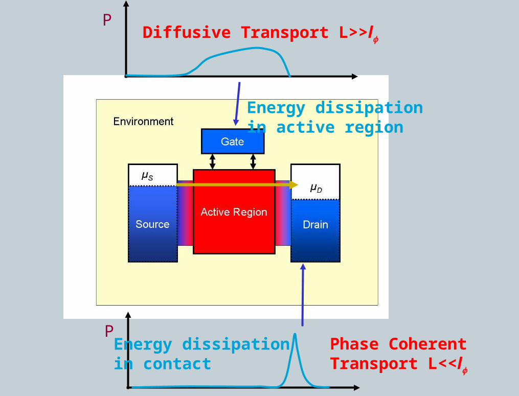
Diffusive Transport L>>l
Phase CoherentTransport L<<l
Energy dissipation in active region
Energy dissipation in contact
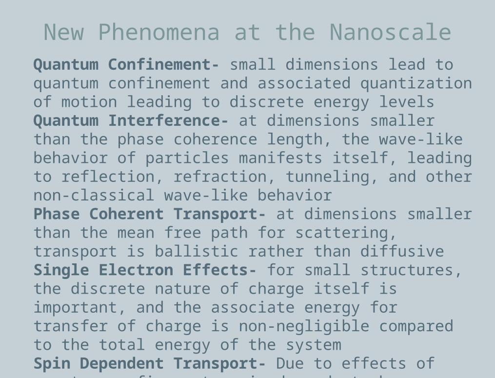
New Phenomena at the NanoscaleQuantum Confinement- small dimensions lead to quantum confinement and associated quantization of motion leading to discrete energy levelsQuantum Interference- at dimensions smaller than the phase coherence length, the wave-like behavior of particles manifests itself, leading to reflection, refraction, tunneling, and other non-classical wave-like behaviorPhase Coherent Transport- at dimensions smaller than the mean free path for scattering, transport is ballistic rather than diffusiveSingle Electron Effects- for small structures, the discrete nature of charge itself is important, and the associate energy for transfer of charge is non-negligible compared to the total energy of the systemSpin Dependent Transport- Due to effects of quantum confinement, spin dependent phenomena may be enhanced.
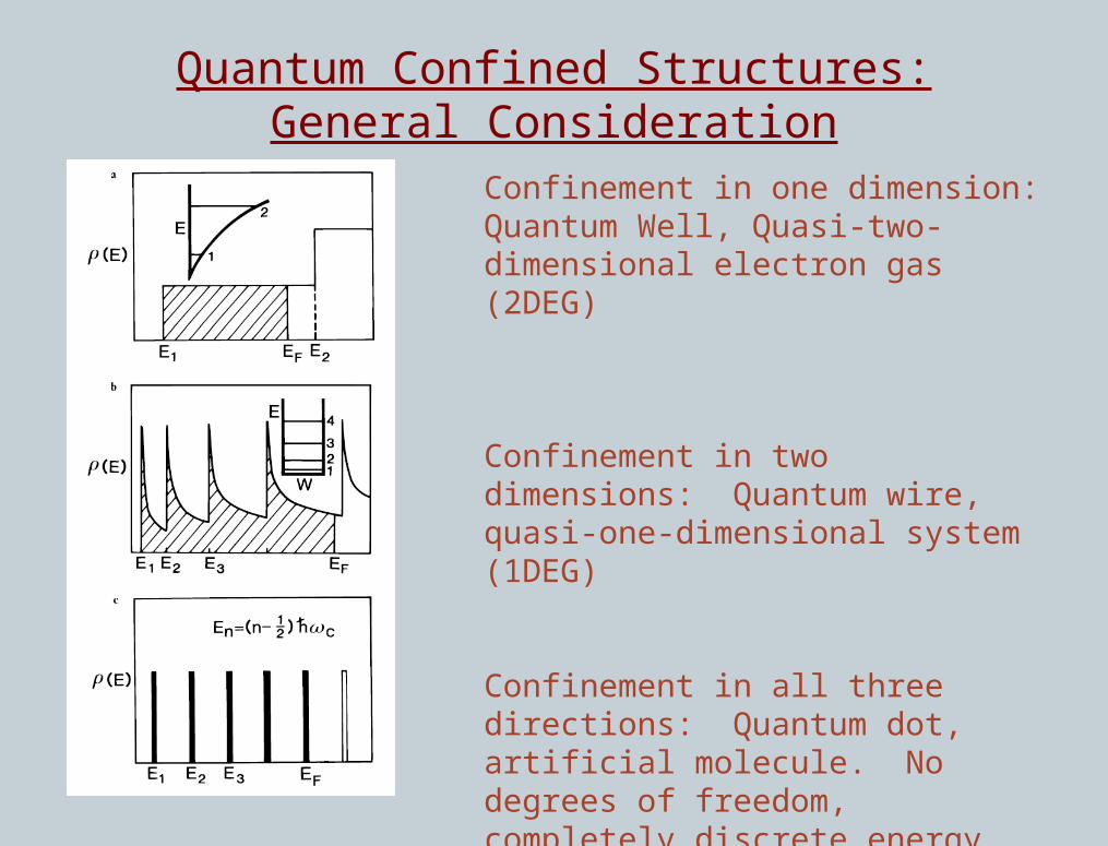
Quantum Confined Structures:General Consideration
Confinement in one dimension: Quantum Well, Quasi-two-dimensional electron gas (2DEG)
Confinement in two dimensions: Quantum wire, quasi-one-dimensional system (1DEG)
Confinement in all three directions: Quantum dot, artificial molecule. No degrees of freedom, completely discrete energy spectrum, singular density of states
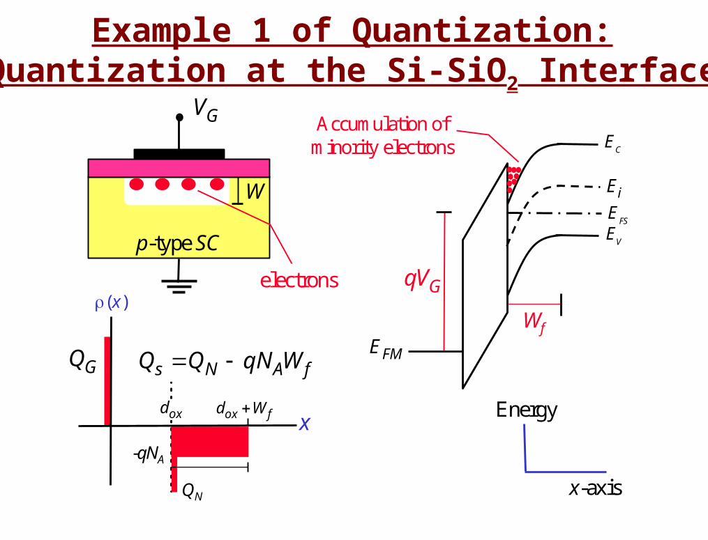
Example 1 of Quantization:Quantization at the Si-SiO2 Interface
GV
oxd
GQ
GqV)(x
x
x-axis
fox Wd
Wf
p-type SC
W
FME
FSE
CE
VE
iE
-qNA
Energy
fANs WqNQQ
QN
electrons
Accumulation ofminority electrons
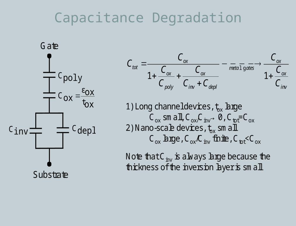
Capacitance Degradation
Substrate
Gate
oxox
ox t
εC
polyC
invC deplC
l g
1 1
ox oxtot meta ates
ox ox ox
poly inv depl inv
C CC
C C C
C C C C
1) Long channel devices, tox largeCox small, Cox/Cinv→0, Ctot=Cox
2) Nano-scale devices, tox smallCox large, Cox/Cinv finite, Ctot<Cox
Note that Cinv is always large because thethickness of the inversion layer is small
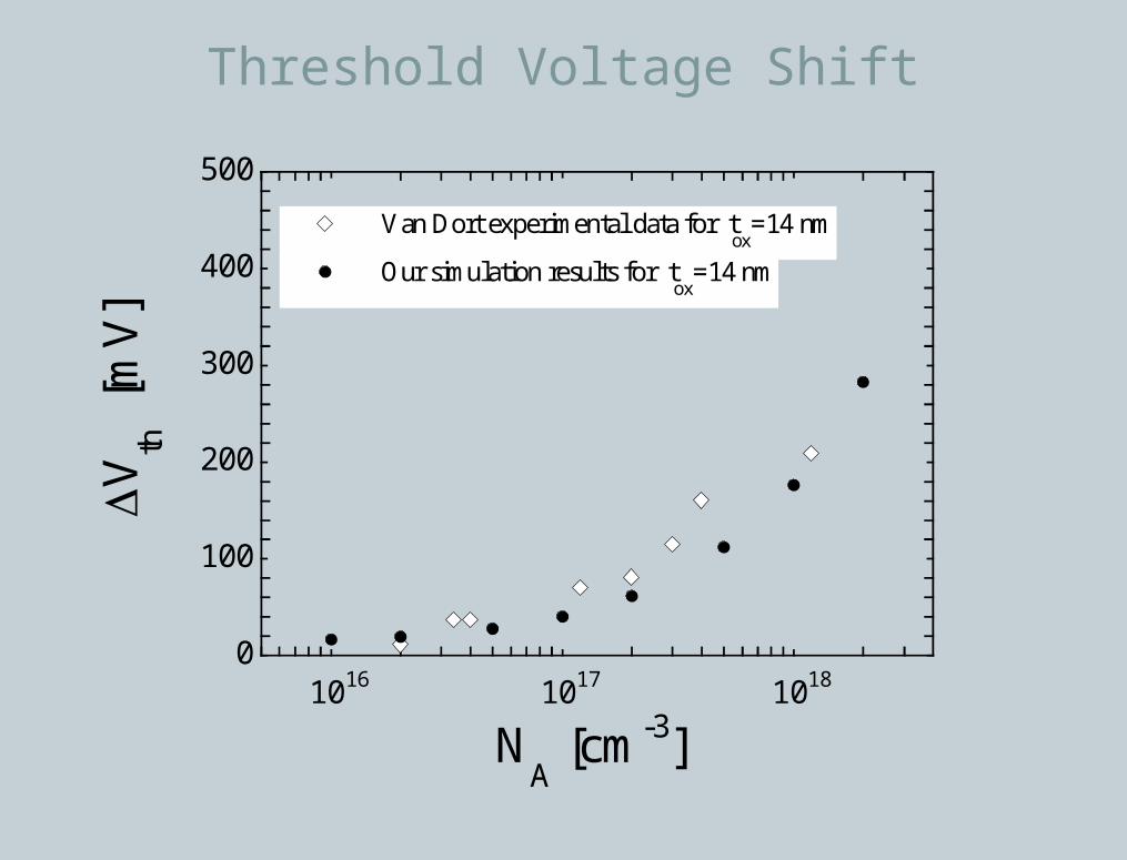
Threshold Voltage Shift
0
100
200
300
400
500
1016 1017 1018
Van Dort experimental data for tox
=14 nm
Our simulation results for tox
=14 nm
Vth
[m
V]
NA [cm-3]
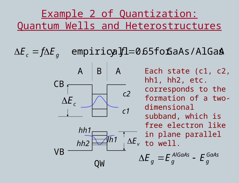
Example 2 of Quantization:Quantum Wells and Heterostructures
sGaAs/AlGaAfor 65.0y empiricall fEfE gc
A AB
CB
VBQW
c1
c2cE
vEhh1
hh2 lh1
Each state (c1, c2, hh1, hh2, etc. corresponds to the formation of a two-dimensional subband, which is free electron like in plane parallel to well.
GaAsg
AlGaAsgg EEE
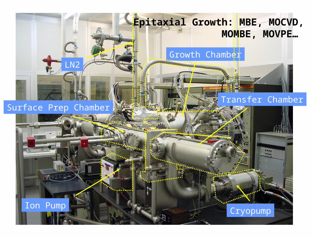
Transfer Chamber
Cryopump
Surface Prep Chamber
Ion Pump
Growth ChamberLN2
Epitaxial Growth: MBE, MOCVD, MOMBE, MOVPE…
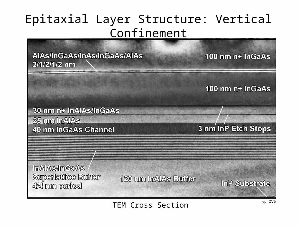
Epitaxial Layer Structure: Vertical Confinement
TEM Cross Section
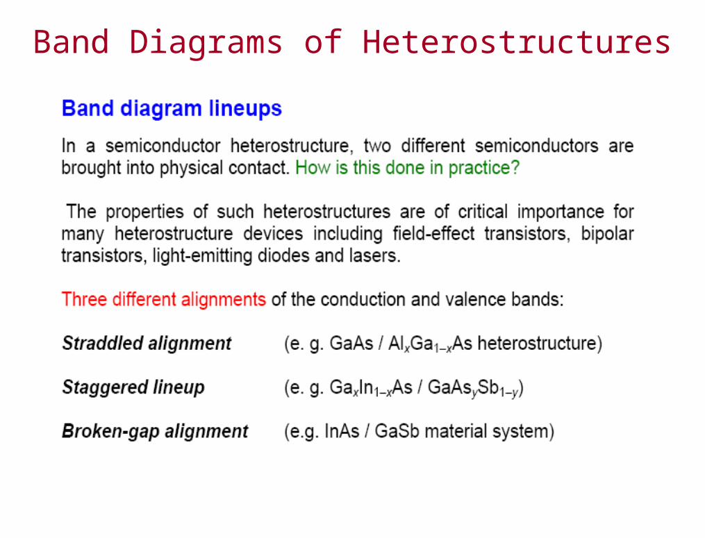
Band Diagrams of Heterostructures
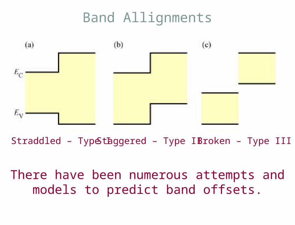
Straddled – Type I Staggered – Type II Broken – Type III
There have been numerous attempts and models to predict band offsets.
Band Allignments
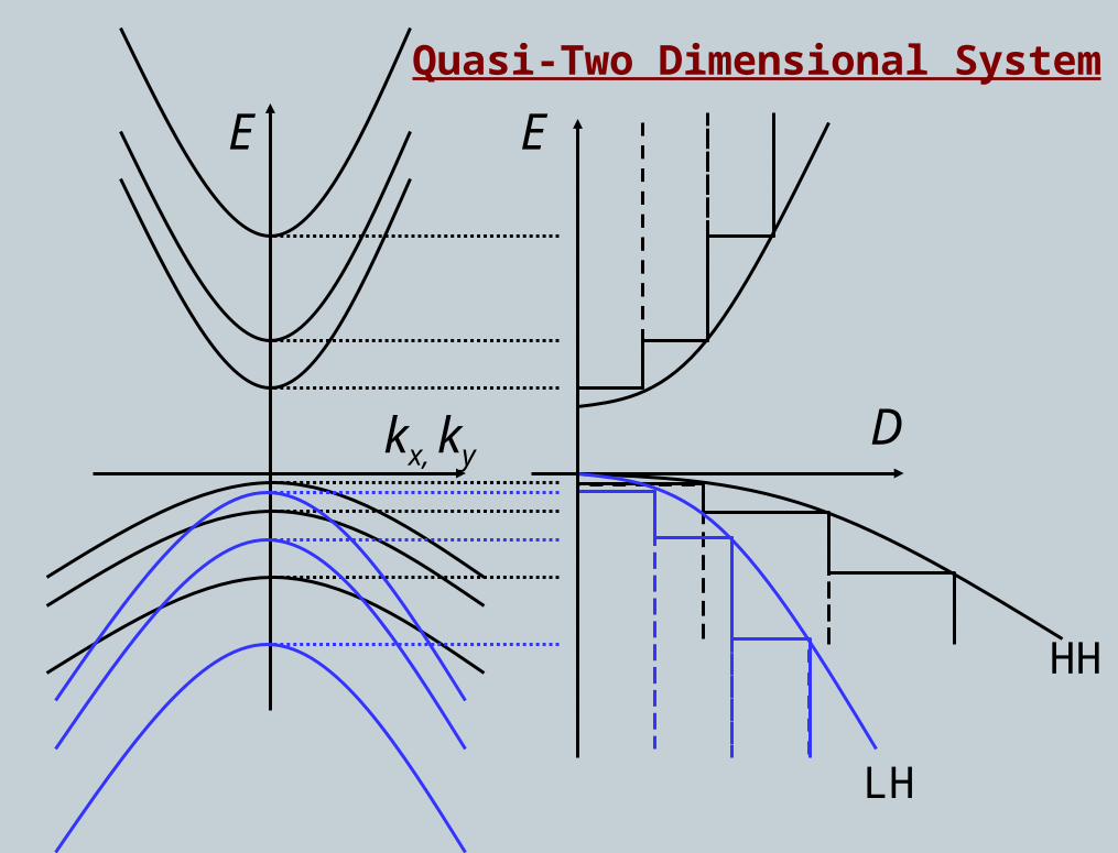
kx, kyD
E
HH
LH
E
Quasi-Two Dimensional System