Embed Size (px)
Citation preview
Contact Evolution in Micromechanical Switches: an experimental investigation using a contact test station
A Thesis Presented
by
Lei Chen
to
The Department of Electrical and Computer Engineering
in partial fulfillment of the requirements for the degree of
Doctor of Philosophy
in
Electrical Engineering
in the field of
Electronic Circuits and Semiconductor Devices
Northeastern University Boston, Massachusetts
August 2007
Contact Evolution in Micromechanical Switches Abstract
I
Abstract
Even though MEMS switches have superior performance relative to other RF
switches, applications of MEMS switches are still limited by reliability problems during
operation. The switches are typically “fail to open” or “fail to close” as the number of
switching cycles increases. In order to understand failure mechanisms in ohmic-type
MEMS switches, a Scanning Probe Microscope (SPM) based test station is designed and
used to study contact evolution. In particular, two failure mechanisms, adhesive failure
and contamination failure were investigated.
The mechanism of adhesive failure is studied in gold contacts. The magnitude of
the pull-off force, the force vs. displacement curves, and the rate-dependent pull-off force
are sampled during cycling. It is found that ductile separation causes significant and
random modification of the contact surfaces. The magnitude of the pull-off force also
changes due to the variation of surface morphology. Significant plastic deformation
during ductile separation can form a plateau region in the force-displacement curve which
is characteristic of ductile separation. This deformation can also contribute to a higher
pull-off force when the contacts are cycled at 300Hz compared with cycling at 0.5Hz.
Adding 5% Ru to the gold can significantly reduce ductile separation and can lower the
pull-off force.
Contamination failure is studied by comparing contact resistance evolution among
gold (Au), platinum (Pt), rhodium (Rh), ruthenium (Ru), and their alloy with gold (Au).
Buildup of contaminants is indicated by increasing contact resistance during the cycling
tests which are performed in room air. These observations suggest that Rh, Ru, and Pt are
Contact Evolution in Micromechanical Switches Abstract
II
prone to contamination failure as contact materials in MEMS switches. The nobleness of
the gold alloys is related to the concentration of alloy element. Higher concentrations of
alloy elements show higher contamination rates.
Contact Evolution in Micromechanical Switches Acknowledgements
III
Acknowledgements
I would like to express my greatest gratitude to my thesis advisor, Professor Nicol
McGruer for his supervision, advice and guidance during the last 6 years. Thank him for
giving me extraordinary experiences through out the work. He has provided me not only
research assistantship over almost six years, but also academically and emotionally
support through the rough road to finish this thesis. I want to extend my appreciation for
his patience, for his great understanding, and for the lessons he gave me.
I would also like to express my deepest appreciation to my thesis co-advisor
Professor George Adams. He has always being available and this thesis would not have
been possible without his help, suggestion and enlightening discussion.
I would like to thank Professor Nicol McGruer and Professor George Adams for
the critical review of the publications that this work has generated, as well as the
manuscripts leading to the final version of this dissertation.
I am grateful to Professor Nicol McGruer, Professor George Adams and Dean
Paul Zavracky for forming part of my Ph.D. committee. I feel honored by having three of
the best professors in the Northeastern University in my committee.
I also thank Dr. Kevin Leedy from Air Force Research Laboratory for thin film
preparation and material testing. I wish to thank Dr. Kevin Gilbert from AFIT for his
kind discussion and structure calibration.
I would like to express my gratitude to the rest of faculty, staff, and colleagues at
the Microfabrication Laboratory (MFL) Group and the Center for High-Rate
Contact Evolution in Micromechanical Switches Acknowledgements
IV
Nanomanufacturing (CHN) at Northeastern University for their support and help. In
particular, I wish to thank Professor Jeffery Hopwood. It has been a pleasure taking class
with him. I wish to thank cleaning room director Richard DeVito and cleaning room
manager Scott McNamara for helping me with my experiments. I wish to thank Juan
Carlors Aceros, ChiaLing Chen, Yan Du, Jim Guo, Felipe Iza, Jeffrey Johnson, Kurt
Joudrey, Xue Jun, Fengchun Li, Neil Mao, Peter Ryan, Sivasubramanian Somu,
Selvapraba Selvarasah, Xiaomin Yan, Xiaoji Yang for their friendship. They have helped
me and taught me immensely at Northeastern University.
My special thanks go to Peter Ryan, thank him for editing this thesis and always
ready to lend me a hand.
Special words of appreciation go to people who have kept encouraging me to
finish this degree in the past three years. Many thanks go in particular to Chris Cruz for
believing in me; Thanks to my dear cousin Yuexin Chen for calling me and encouraging
me. Thanks to Ziyi Zhou and YangPing Zhang for inviting me to their many great dinner
parties. Thanks to Jun Yue for sharing with me her music. All these love and friendship
enable me to complete this work.
I am particularly indebted to my younger brother Xi Chen. He has taken care of
our parents at home while I am studying in the United States. Thank him for being
supportive.
Lastly, and most importantly, I wish to express my most sincere gratitude to my
parents, Houlun Chen and Yanrong Zhou. They bore me, raised me, taught me, and loved
me. The support and love they have demonstrated over and over again cannot be
overemphasized. It is to them I dedicate this thesis.
Contact Evolution in Micromechanical Switches Acknowledgements
V
During my studies at Northeastern University, I have had the privilege of
receiving financial support from DARPA under its HERMIT program through research
contract F33615-03-1-7002.
Boston, Massachusetts
August 2007
Contact Evolution in Micromechanical Switches Table of Contents
VI
Table of Contents
1 Introduction................................................................................................................. 1 2 Reliability Problems.................................................................................................... 2 3 Contact Reliability Test Methods ............................................................................... 9
3.1 On-Chip Device Testing ..................................................................................... 9 3.2 Piezo-Controlled Contact Test.......................................................................... 13 3.3 Challenges of Contact Study............................................................................. 19 3.4 SPM for Contact Study ..................................................................................... 21
4 SPM Based Contact Test System.............................................................................. 25 4.1 Setup of the Contact Station ............................................................................. 25 4.2 Operation Principle ........................................................................................... 27 4.3 Contact Cantilever and Fabrication .................................................................. 29 4.4 Contact Bump Fabrication ................................................................................ 34 4.5 Contact Angle and Sliding ................................................................................ 36 4.6 Environmental Control for Contact Test........................................................... 38
5 Adhesive Failure in Contact Evolution..................................................................... 41 5.1 Contact Adhesion.............................................................................................. 41 5.2 Separation of Adhesive Contacts ...................................................................... 44
5.2.1 Two Separation Modes ............................................................................. 44 5.2.2 Crack Propagation and Griffith Concept .................................................. 47 5.2.3 Cleavage and Dislocation Nucleation....................................................... 49 5.2.4 Pull Off Force ........................................................................................... 53 5.2.5 Force Measurement................................................................................... 54
5.3 Rate Dependent Pull-Off Force and Separation Modes.................................... 57 5.3.1 Introduction............................................................................................... 57 5.3.2 Rate Dependant Pull Off Force................................................................. 59 5.3.3 Rate Effects in Brittle Mode ..................................................................... 68 5.3.4 Rate Effects in Ductile Mode.................................................................... 72
5.4 Contact Evolution and Separation Modes......................................................... 83 5.4.1 Force Evolution in Au/Au Contacts.......................................................... 83 5.4.2 Ductile Separation in Contact Evolution .................................................. 86 5.4.3 Modes Transition in Contact Evolution.................................................... 91
5.5 Size Effects on Adhesive Failure...................................................................... 97 5.6 Material Effects on Adhesive Failure ............................................................... 99 5.7 Conclusions..................................................................................................... 102
6 Contamination Failure in Contact Evolution .......................................................... 105 6.1 Introduction..................................................................................................... 105 6.2 Nobleness of Gold and Gold-Alloys............................................................... 107
6.2.1 Film Preparation [77] ................................................................................ 107 6.2.2 Contact Resistance .................................................................................. 109 6.2.3 Evolution of Contact Resistance............................................................. 116
6.3 Absorption of Molecule .................................................................................. 119 6.3.1 Adsorption Processes [81]......................................................................... 119 6.3.2 Newns-Anderson Model [81].................................................................... 120 6.3.3 D-band Theory [82]................................................................................... 121
Contact Evolution in Micromechanical Switches Table of Contents
VII
6.4 Competition of Failure Mechanism ................................................................ 124 6.5 Conclusions..................................................................................................... 126
7 Conclusion and Future Work .................................................................................. 128 7.1 Conclusions..................................................................................................... 128 7.2 Future work..................................................................................................... 131
Appendix I: Sandwich Structure for Sliding Cancellation ............................................. 133 Appendix II: Preparation for Cycling Test ..................................................................... 137 Appendix III: Fabrication of Round Bump with Different Radii ................................... 139 Appendix IV (a): Fabrication Process for Backside Etching.......................................... 142 Appendix IV (b): Fabrication Process for Round Bump ................................................ 145 Appendix IV (c): Fabrication Process for Cantilever ..................................................... 147 References....................................................................................................................... 150
Index of Figures Figure 2-1: Metal contact failure modes: (a) material transfer due to the ductile
separation; (b) contamination building up around the contact bump ......................... 5 Figure 3-1: The contact test results from Majumder’s work [17]: (a) shows the resistance-
vs-force characteristic curve at the early stage of the contact test. The contact resistance is 0.7Ω, and the adherence force is 20μN corresponding to the loading force 70 μN; (b) shows the resistance-vs-force characteristic curve after 1000 cycles test. After the cyclic test, the contact resistance dropped to 0.1Ω, and the adherence force increased to 50 μN. .......................................................................................... 10
Figure 3-2 [14]: Schematic of Schimkat’s experimental setup. The force is measured by the
force sensor cell and the displacement is generated by the piezotranslator.............. 14 Figure 3-3 [6]: IFM profiles with force and contact resistance plotted as a function of
relative displacement between the tip and substrate. Repulsive forces are shown as positive and attractive forces are negative. Contact resistances are measured at constant current source 10 μA: (a) is a representative profile of IFM test in a N2 at the room temperature. The sample is tested before the ozonation. Adhesion is barely detected. The minimum contact resistance is about 9Ω. (b) is a representative profile of IFM test in the UHV. The maximum detected attractive force is about 45 μN, with a contact resistance is about 0.8Ω. Notice that, at the displacement location of 20nm, the attractive force suddenly decreases to 20~30 μN, and the contact resistance jump to 100 Ω. This indicates there is connective necks due to plastic deform of the gold contact. ....................................................................................... 17
Figure 3-4: Schematic representation for the approaches of the contact study ................ 20
Contact Evolution in Micromechanical Switches Table of Contents
VIII
Figure 3-5: Schematic description of the force measurement mechanisms, (a) SPM, and (b) Force Sensor Cell ................................................................................................ 23
Figure 4-1: Schematic of the AFM based contact ............................................................ 26 Figure 4-2: Illustration of the force measurement principle of SPM. (a) An optical lever
system is used to detect the deflection of the cantilever; (b) the deflection causes a movement of laser spot on the photo detector. ......................................................... 28
Figure 4-3: Illustration of the cross section structure of cantilever, (a) rectangle, (b)
trapezoid.................................................................................................................... 30 Figure 4-4: Microfabrication flow chart for silicon cantilever ......................................... 32 Figure 4-5: Micrograph of fabricated contact cantilever ( a ) with trapezoidal cross
section; ( b ) with rectangular cross section.............................................................. 33 Figure 4-6: SEM micrographs of fabricated contact bumps: (a) contact bump with flat
top; (b) hemispherical contact bump made using a gas ratio of O2:SF6=20:10; (c) hemispherical contact bump made using a gas ratio of O2:SF6=15:10.................... 34
Figure 4-7: SEM micrograph of a patterned photoresist Shipley 1818: (a) before reflow;
(b) after the reflow. ................................................................................................... 35 Figure 4-8: Contact angle set-up for cyclic test. Wedge is used to keep the planar
substrate parallel to the cantilever............................................................................. 37 Figure 4-9: Nitrogen flow set-up for the environmental control. ..................................... 39 Figure 4-10: Ruthenium contact tests with and without nitrogen flow. Nitrogen flow rate
was 500sccm. ............................................................................................................ 40 Figure 5-1: Schematic description of the adhesion between two surfaces. ...................... 42 Figure 5-2: Molecular dynamic simulation of Au/Au contact.......................................... 46 Figure 5-3: Crystal plan sliding, atomic-scale plasticity [46] ............................................. 50 Figure 5-4: Competition between cleave and dislocation [47] ........................................... 51 Figure 5-5: The curve measured during a contact opening using the Scanning Probe
Microscope. The schematics describe the contact states corresponding to the force measurement. ............................................................................................................ 55
Figure 5-6: Force displacement curve for two separation modes. Both force-displacement
curves were measured at the unloading rate of 35µm/s............................................ 56
Contact Evolution in Micromechanical Switches Table of Contents
IX
Figure 5-7: SEM micrograph of the gold samples interfaces with maximum loading force
at 200 μN. (a) the bump with the radius of curvature of 4µm, the pull off force at 0.5Hz is 172±11μN and pull off force at 300Hz is 94 ±9.5μN; (b) the bump with the radius of curvature of 50 µm, the pull off force at 0.5Hz is 130±9.7μN, and the force at 300Hz is 165±7.2μN. ............................................................................................ 61
Figure 5-8: The rate dependent response of the pull off force by sweeping the cycling
rate. The maximum loading force is maintain at 200µN. (a) is the pull off force response for cycling number less than 105; (b) is the response after 106 number cycles test .................................................................................................................. 62
Figure 5-9: Rate dependent pull off force for separation with (a) larger force at low rate,
and (b) larger force at high rate................................................................................. 63 Figure 5-10: Schematic representation of meniscus formation at the interface for: (a) a
sphere in contact with a plane surface, ( b ) a sphere flattened with an effective radius in contact with a plane surface. ...................................................................... 70
Figure 5-11: SEM micrograph of the surface after ductile failure. This separation
occurred after a single load-unload cycle with a maximum loading force of 250µN.................................................................................................................................... 72
Figure 5-12: Pull off force test with different unloading velocity. (a) The driving
waveform for the test. Each pulse with the same loading slope and the same time in contact, however, the unloading slop is different; (b) measured unloading rate dependent pull off force in the ductile mode. ........................................................... 82
Figure 5-13 Change in pull off force in a hemispherical/flat contact with cycling for Au
contacts at 250µN ..................................................................................................... 84 Figure 5-14: SEM micrograph of gold contact bump after ( a ) 100 cycles, (b) 1000
cycles......................................................................................................................... 85 Figure 5-15: SEM micrograph of gold contact bump after 1000000 cycles: (a) sample 1;
(b) sample 2; and (c) sample 3.................................................................................. 86 Figure 5-16: Force displacement curves show the increasing of the pull off force after the
onset of ductile separation ........................................................................................ 87 Figure 5-17: Force displacement curves show the decreasing of the pull off force after the
onset of ductile separation ........................................................................................ 89 Figure 5-18: Modes transition during the evolution of samples with bump radius of
curvature of: (a) , (b) 4µm; (c), (d) 15 µm; (e),(f) 22 µm; and (g), (h) 50 µm. ....... 93
Contact Evolution in Micromechanical Switches Table of Contents
X
Figure 5-19: Force evolution curve of a gold contact show the separation mode transit from ductile to brittle. ............................................................................................... 95
Figure 5-20: SEM Micrograph of the gold bump after 3x10⁵ cycling test. ...................... 96 Figure 5-21: Force displacement curve recorded during the cycling test. ........................ 97 Figure 5-22: Pull off force and its relation to the bumps size and the separation modes. 98 Figure 5-23: The pull off force for Au_5%Ru alloy with three different contact radius of
curvature (15µm, 22µm and 50µm). Maximum loading force is 200µN. .............. 100 Figure 6-1: Cantilevers for contact tests: SEM micrographs of (a) contact bump and (b)
silicon cantilever; Test layout for contact resistance measurement. (c) Substrate and (d) cantilever. .......................................................................................................... 111
Figure 6-2: Electrical resistivity (a) and measured total resistance (b) for various thin
films with hardness measured at a 24 nm indentation depth. ................................. 112 Figure 6-3: Measured total resistance, ANSYS simulated total resistance value, and
calculated single asperity constriction resistance. .................................................. 114 Figure 6-4: The ratio of the ANSYS simulated resistance to the measured total resistance
for various thin films............................................................................................... 115 Figure 6-5: Measured total resistance (including contact resistance and sheet resistance
components) evolution curves of, (a) Ru, Pt, Rh and Au; (b) Au and Au-Ru alloys; (c) Au and Au alloys ............................................................................................... 118
Figure 6-6: SEM and EDX analysis of Au-30%Rh alloy contact surface after cycling test.
(a) SEM micrograph; (b) EDX spectrum at three different locations on the bump: i) top of bump; ii) dark contaminant; iii) clean surface.............................................. 119
Figure 6-7: The local density of stats at an adsorbate in the Newns-Anderson model in
two limiting cases: (a) the ∆(ε) independent of ε; and (b) for a narrow metal band................................................................................................................................ .121
Figure 6-8: Graphic description of the d-band theory .................................................... 122 Figure 6-9: SEM micrograph of Au-Ru alloy contact surface after 106 cycles test. (a)
Au_10%Ru bump surface, (b) Au_5%Ru bump surface........................................ 125 Figure 7-1: Contact angle set-up for cyclic test. Two wedges are used to cancel the
sliding movement during the actuation. Wedge 2 is used to provide an actuation angle and wedge 1 is used to keep the substrate parallel to the cantilever. ........... 133
Contact Evolution in Micromechanical Switches Table of Contents
XI
Figure 7-2: SEM micrograph and AFM 3D image of fabricated silicon bumps with radius of curvature of (a) 4µm; (b)15 µm; (c)22 µm and (d) 50 µm................................. 141
Index of Tables Table 4-1: Measured dimension of two cantilevers (C_A and C_B) and their estimated
stiffness ..................................................................................................................... 33 Table 5-1: Viscous force estimation according to the dimension of the structure............ 81 Table 6-1: (a) Hardness, modulus and resistiviy; (b) deposition power and rate; for single
metal and co-sputtered metal films. ........................................................................ 108
Contact Evolution in Micromechanical Switches Introduction
1
1 Introduction
Switches are fundamental elements in the electrical circuits. The switching function
is usually implemented with solid state devices, such as PIN diodes and field effect
transistors (FETs). MEMS switches, devices based on micromachining processes, were
originally introduced by IBM in 1979[1]. For MEMS switches, the function of “open” or
“closed” circuits is realized by mechanical movements of a cantilever beam, a fixed-fixed
beam, or a membrane [2].
Like reed relays, the contacts of MEMS switches are physically separated by an air
gap. In order to close the circuit, a driving force, such as an electrostatic force,
electromagnetic force, or thermal force can be used to pull the contacts together. These
contacts are either resistive type, metal-to-metal contacts or capacitive type, dielectric-
metal contacts. Capacitive switches are particularly designed for the RF current bridging.
Due to the air gap between the contacts, the MEMS switches usually have high isolation
at the “open” state. The physical contact between the cantilever and the substrate can also
provide a low insertion loss in the “closed” state. Compared to PIN diode and FET
switches, the MEMS switches have a wider frequency response range (DC-100GHz),
higher signal linearity and lower power consumption. These advantages make MEMS
switches good candidates for RF applications. Potential applications of MEMS switches
include radar systems, satellite communication system and wireless communication
systems [3]. Generally, all these applications require that the switches work (open and
closed) for one billion to one trillion cycles [4]. Therefore, knowing how to improve the
durability of the MEMS switches becomes important.
Contact Evolution in Micromechanical Switches Reliability Problems
2
2 Reliability Problems
The most intractable reliability problems in MEMS switches come from the two
contacting surfaces. Reliable operation generally requires the surfaces have both
mechanical and electrical stability. The dominant failure mechanism is different for
capacitive-type switches and resistive-type switches. In the case of capacitive switches,
the reliability problems are mainly caused by charges at the dielectric surface. The
trapped charges on the dielectric surfaces can hold the membrane and substrate together,
which leads to “stiction” failure. However, the charge is not usually an issue for the
resistive-type switches. In the case of metal-to-metal contacts, factors such as mechanical
impacts, surface morphology and thermal dissipation are important for the long-term
performance of the contacts. The metal-to-metal contact can either “fail to open” or “fail
to close”, depending on the dominant failure mechanism. This thesis will focus on
studying failure mechanisms of metal-to-metal contacts.
The “fail to open” mode is usually caused by the two contacts surfaces sticking to
each other, often called the “stiction” problem. The “stiction”, or excessive adherence
force between the two sides of the contact, can be enhanced by factors such as surface
films (or the lack of surface films), thermal dissipation, contact creep and ductile
separation.
Surface films: In MEMS switches, the contact surface is usually covered by a
thin layer of surface film (2 ~5nm) due to absorbed molecules on the surface.
The surface energy is strongly affected by the surface conditions. The surface
Contact Evolution in Micromechanical Switches Reliability Problems
3
energy for clean metal is about 1 ~3J/m2, and the surface energy for molecular
crystals is less than 0.1J/m2 [5]. If the metal surface is covered by a thin layer
of absorbed atoms, the surface energy is greatly reduced due to the molecular
screening effect. The surface film is believed to serve as a passivation layer
for preventing strong adhesion between clean metal-to-metal contacts [6].
During the switching operation, the surface film can be progressively removed
or interrupted because of mechanical or the electrical effects. Damage to the
surface film can increase the area of the metal-to-metal contact. The strong
adhesion of direct metal-to-metal contact will increase the adherence force,
which is the force needed to open the contact. When the adherence force is
larger than the maximum available restoring force of actuator, the contact will
fail to open.
Thermal dissipation: The thermal dissipation directly determines the power
handling ability of the MEMS switches. Due to the resistance between the
contacts, when the current is passing through the contacts, there is the thermal
dissipation. The thermal dissipation can locally increase the temperature
around the contact area. Based on Holm’s theory, the contact temperature
corresponds to the voltage crossing the contacts. For the gold-on-gold contact,
soften, melting and boiling temperature are 100 ºC, 1063 ºC and 2817 ºC ,
respectively, and corresponding contact voltages are 70mV, 430mV and
900mV [7]. Thermal dissipation can soften the contacts, reduce the contact
hardness and increase the contact area. It will increase the adherence force
Contact Evolution in Micromechanical Switches Reliability Problems
4
simultaneously. If the contact temperature reaches the melting point of the
metals, the two contacts can be thermally welded to each other.
Contact creep: When a load is applied to a material, its strain response
consists of a rapid elastic deformation related to the Youngs’ modulus and a
time dependant term. The latter is due to creep. The classical definition of
creep is “a time-dependent deformation of a sample caused by external
mechanical loads”. Most metals exhibit creep at temperatures higher than 1/3
of their melting points. However, at room temperature, high stresses and stress
gradients introduce the possibility of time-dependent mass transfer through
glide and diffusion mechanisms [8]. Surface tension has been believed to cause
the material diffusion around nanoscale contact spots [9]. The creep can
increase the contact area, and in turn, increase the adherence between the
contacts.
Ductile separation: Ductile separation occurs during the unloading of the
contacts. If there is strong adhesion between the contact surfaces, the
unloading procedure stretches the contact materials to form a conductive
“neck”. The rupture of this conductive neck may happen at the original
interface, or may happen inside of the contact materials, which depends on the
magnitude of the contact adhesion and the tensile strength of the materials.
Once the rupture of the contacts occurs inside of the bulk materials, instead of
the interface, the material can transfer from one side of the contact to the
other. The physical mechanism will be discussed in detail in this thesis. After
many cycles of material transfer occurs, the contact surface may be seriously
Contact Evolution in Micromechanical Switches Reliability Problems
5
damaged. The progressive ductile stretching and necking can generate the
“microbridges” or “nanowires” between the two contact surfaces. With these
“microbridges” or “nanowires”, the switch may keep connected, even after the
cantilever beam is mechanically moved away. It contributes to another
mechanism of the “fail to open”. Material transfer can be enhanced by either
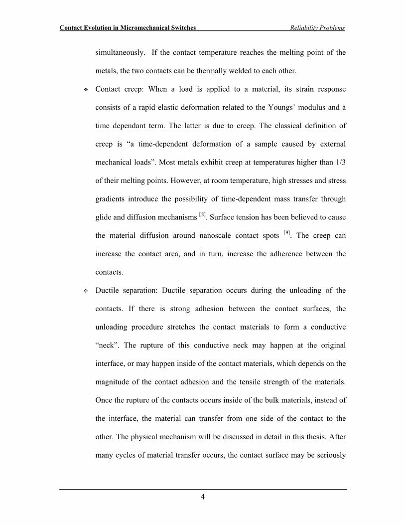
mechanical impacts or the current effect [10].
( a ) ( b )
Figure 2-1: Metal contact failure modes: (a) material transfer due to the ductile separation; (b) contamination building up around the contact bump
These four factors can interact with each other to accelerate the failure process.
For instance, the current or thermal effect can break the surface film and lead to more
metal-to-metal contact. Increasing the temperature around the contact area can also
activate the contact creep. The interposing of the surface film will increase the contact
resistance, in turn, cause more energy dissipation around contact area. The material
transfer can be accelerated by current softening effects or be decelerated by interposing
surface film.
The “fail to closed” mode is caused by the increasing of the contact resistance
during the switching operation (from 1~2Ω to 10~100 Ω or more). The typical
Contact Evolution in Micromechanical Switches Reliability Problems
6
mechanism related to this failure mode is the building up of an insulating layer on the
contact surfaces. These insulating layers can be surface films or frictional polymer. The
building-up rate of these contaminants is related to the contact material properties and the
environmental effects.
Surface Film: The surface film is mainly due to absorption of molecules on
contact surfaces. Generally, Au is noble and has a clean surface. However, a
2~4 nm thick hydrocarbon insulating thin film is observed on the gold surface
[11]. This film may come from the fabrication residues or absorption from the air
during switching operation. Because of the surface film, the contact resistances
are high and unstable in the low force region (<100μN [6,12]). A higher contact
force is necessary to get desirable and stable contact resistance. During cyclic
contacts, the film may be removed or may accumulate around the contact spots.
These effects can result in unstable contact resistances. The deleterious effect of
surface films can be limited by higher force and larger current [13,14].
Frictional Polymer [15]: Frictional polymer come from chemical reactions on the
contact surfaces. Based on the research from reed relays, refractory metals, such
as Rh, Ru, Pt and Pb, can easily be contaminated in the room air. There is a
nonconductive polymer thin film developed on the contact surfaces during
cyclic testing. The mechanism of polymer formation is not clear. It is believed
that this phenomenon is related to the reactivity of the contact surface. The
refractory metal can absorb the organic vapor from the environment. At the
same time, the metal surface can also serve as a catalyst for chemical reactions.
Contact Evolution in Micromechanical Switches Reliability Problems
7
Due to the catalysis effects, the absorbed organic molecules will interact with
each other and form a cross-linked polymer on the metal surfaces. The polymer,
also called “frictional polymer”, will increase the contact resistance. In order to
prevent the contamination, the MEMS switches are usually hermitically
packaged an inert gas (N2 or Ar). The hermetic packaging increases the overall
cost of the fabrication. At the same time, the out-gassing from the package
material can still cause contamination in the metal contacts.
Some resistance increase could also be due to the hardening effects of the
contacts. The contact area is inversely proportional to the hardness of the contact
surfaces. Increasing of the hardness can reduce the contact area for the current
conduction. Strain hardening may be one possible mechanism. One other possible
mechanism can be related to the “microbrides” or “nanowires” formed due to the ductile
separation. The micro/nano necks may roughen or harden the contact surface. However,
the “microbriges” and “nanowires” effects are still under investigation.
When the switches are operated while a voltage is placed across the contact
during loading and unloading, or say hot-switching, there may be discharges (or arcs)
between the contact surfaces. These discharges can cause erosion of the contact surface
and deposition of organic and inorganic debris on the contact surfaces [16]. In order to
avoid these violent damages, the MEMS switches are usually operated in the cold-
switching mode, such that the current is applied after physical contact is made.
Due to reliability problems, switches usually fail when the number of cycles
increases beyond 109 cycles. Only the switches from Radant MEMS, Inc. have been
Contact Evolution in Micromechanical Switches Reliability Problems
8
reported to have stable operations up to 2 ~3×10¹¹ cycles [4]. However, the physical
mechanism of failure mode is still not well understood. In order to solve the reliability
problem, it is important to understand the contact physics at the micro and nano scale.
This thesis will focus on studying the failure mechanisms of metal-to-metal contacts
when cycled, and the primary focus will be on the mechanical effects on contact
evolution.
Contact Evolution in Micromechanical Switches Contact Reliability Test Methods
9
3 Contact Reliability Test Methods
Several approaches have been carried out to study the contact failure mechanisms.
Depending on the testing setup methods, these approaches can be sorted as: on-chip
device testing [17,18, 19] and piezo-control contact testing [6, 10, 12, 14, 20]. In this section, I will
review the works of these researchers and the state-of-art of the understanding of contact
failure mechanisms.
3.1 On-Chip Device Testing
On-chip testing is studying contact properties by using on-chip MEMS switches.
It is generally performed by measuring the contact resistance of the MEMS switch during
the cyclic test. Contact resistance depends on the contact area and the interface
properties. Electrical contact resistance (ECR) has been generalized as a diagnostic tool
for MEMS contact interfaces [21]. By monitoring the variation of the contact resistance,
some contact properties can be derived from the resistance evolution curve. Contact force
and adherence force are usually extrapolated from the driving voltage, the structure of the
switch or the opening time. Several important contributions are summarized here.
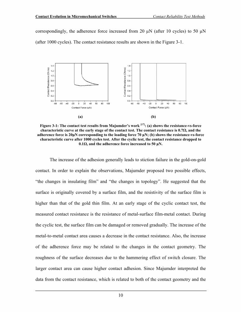
Majumder [17] has tested MEMS switches with gold-on-gold contacts under
different contact loads. During the cyclic test, the contact resistance and contact
adherence are measured. When the contact force was held constant at 70µN, the contact
resistance decreased from 0.6 Ohm (after 10 cycles) to 0.1 Ohm (after 1000 cycles), and
Contact Evolution in Micromechanical Switches Contact Reliability Test Methods
10
correspondingly, the adherence force increased from 20 µN (after 10 cycles) to 50 µN
(after 1000 cycles). The contact resistance results are shown in the Figure 3-1.
(a) (b)
Figure 3-1: The contact test results from Majumder’s work [17]: (a) shows the resistance-vs-force characteristic curve at the early stage of the contact test. The contact resistance is 0.7Ω, and the
adherence force is 20μN corresponding to the loading force 70 μN; (b) shows the resistance-vs-force characteristic curve after 1000 cycles test. After the cyclic test, the contact resistance dropped to
0.1Ω, and the adherence force increased to 50 μN.
The increase of the adhesion generally leads to stiction failure in the gold-on-gold
contact. In order to explain the observations, Majumder proposed two possible effects,
“the changes in insulating film” and “the changes in topology”. He suggested that the
surface is originally covered by a surface film, and the resistivity of the surface film is
higher than that of the gold thin film. At an early stage of the cyclic contact test, the
measured contact resistance is the resistance of metal-surface film-metal contact. During
the cyclic test, the surface film can be damaged or removed gradually. The increase of the
metal-to-metal contact area causes a decrease in the contact resistance. Also, the increase
of the adherence force may be related to the changes in the contact geometry. The
roughness of the surface decreases due to the hammering effect of switch closure. The
larger contact area can cause higher contact adhesion. Since Majumder interpreted the
data from the contact resistance, which is related to both of the contact geometry and the
Contact Evolution in Micromechanical Switches Contact Reliability Test Methods
11
surface films, it is hard for Majumder to figure out the dominant factor for changes in
resistance during contact evolution. The correlation between the contact resistance
evolution and roughness evolution is not clear from the experimental data because few
contacts were imaged.
Jensen [18] studied contact adherence by monitoring the switch opening time. He
tested the switches with apparent contact areas varying from 26.7 to 314µm2 and pull-
apart forces of either 54.4 or 76.6µN. Jensen found the adhesion has a strong effect on the
contact opening time. Generally, the contacts with larger contact size have the higher
adhesion and the longer opening time. The contacts with lower contact resistance have a
larger metal-to-metal area, and in turn, have larger contact adhesion. Based on the
experimental results, Jensen concluded that the contact adhesion corresponds to the
density of clean metal-to-metal bonds. In order to reduce the contact adhesion, a small
contact size is preferred. One interesting observation of Jensen’s experiment is that, when
the contact force is high enough (>160 µN), the switch opening time can be reduced.
Jensen attributed this phenomenon to mechanical vibrations, which are caused by the
large impact force. The mechanical vibration can generate a large transient pull-apart
force, which causes a fast contact opening. Jensen clearly demonstrated the adhesive
effects of the contact size and the surface film. There is no contact evolution data from
the paper, and the author simplified the roughness effects to a single asperity contact. The
failure mechanism of “stiction” is not studied in this work.
Jensen and Chow [13] also studied the Au/Au electrical contact performance at low
contact force (47μN). They found that contact resistances are easily affected by surface
films in the low force region. The contact resistance is observed to slowly increase during
Contact Evolution in Micromechanical Switches Contact Reliability Test Methods
12
mechanical cycling. They think this is because the electrostatic force pulled the
impurities into the contact area. The increase in contact resistance can be prevented by
applying a large current. The current heating can break down the surface film and
guarantee a good metal-to-metal contact. Since the force is low, the contact radius in this
force region is smaller than the electron mean free path in the material (<50nm). Under
these conditions, the current transport should be in the diffusive and ballistic transition
region. Since the boundary-scattered electrons do not heat the contact region, the current
heating effect can be reduced due to the nanoscale contact spots. They observed that the
contact with larger resistance (smaller contact spots) required a higher contact voltage for
heating.
In order to avoid the uncertainty of the force measurement during the contact, a
nano-indenter [22,23,24] can be used for switch testing. The indenter is directly placed on
the top of the switch cantilever for applying the force and monitoring the displacement.
The force manipulation mechanism of the nano-indenter is used to calibrate the stiffness
of the cantilever and measure the force during the contact events. Using this technique,
the contact force and loading displacement can be accurately controlled. Gregori and
Clarke [23] used a nano-indenter to measure the contact adherence after a certain number
of cycles. They observed contact adhesion increasing with the number of actuation
cycles. Coutu [24] also use this technique to characterize their MEMS switches and
evaluate the contact materials. The nano-indenter provides a good tool to characterize the
stationary contact of the MEMS switch. However, the nano-indenter has not been used to
monitor the force condition during the cyclic test. The failure mechanism of the contact is
still not clear from their research.
Contact Evolution in Micromechanical Switches Contact Reliability Test Methods
13
One limitation of the on-chip test is that it’s hard to get in-situ surface analysis.
The switch has to be destroyed to study the surface morphology. The data from the tests
usually failed to demonstrate the relation between surface energy and surface
morphology. The other limitation is that the contact force and adherence force can not be
directly measured during the cyclic test. Due to the limitations of the fabrication, the
method is hard to be used to evaluate the different contact materials and contact
geometry.
3.2 Piezo-Controlled Contact Test
Instead of using MEMS switches, some researchers have used piezoelectric
actuators and force sensors for setting up contact tests. The piezoelectric actuator is used
to control the displacement during loading and unloading the contact. The force sensor
cell is used to monitor and measure the force. The force sensor can either simply be a
spring, such as a spring cell [14] or leaf spring [12], or be a sensor cell with the spring and a
position sensor, such as linear variable differential transformer (LVDT) [10], nano-
indenter [20] and Interface Force Microscope [6] . The stiffness of the spring is calibrated,
and the force is given by the displacement of the spring times the stiffness. In order to
study the contact physics, a probe and a planar surface are used for the contact test. Both
the probe and the planar surface are coated with contact materials, and either the probe or
the planar surface is attached to the piezoelectric actuator for contact test and force
measurement. The peizo-controlled setup can provide a precise adjustment and a
continuous variation of the contact force. The contacts can be brought in contact without
any disturbing impact. This feature is especially preferred when we are interested in the
Contact Evolution in Micromechanical Switches Contact Reliability Test Methods
14
low force contact properties [14]. Additionally, this technique can be easily used for
evaluating contact materials. The surface is available for analysis without damaging the
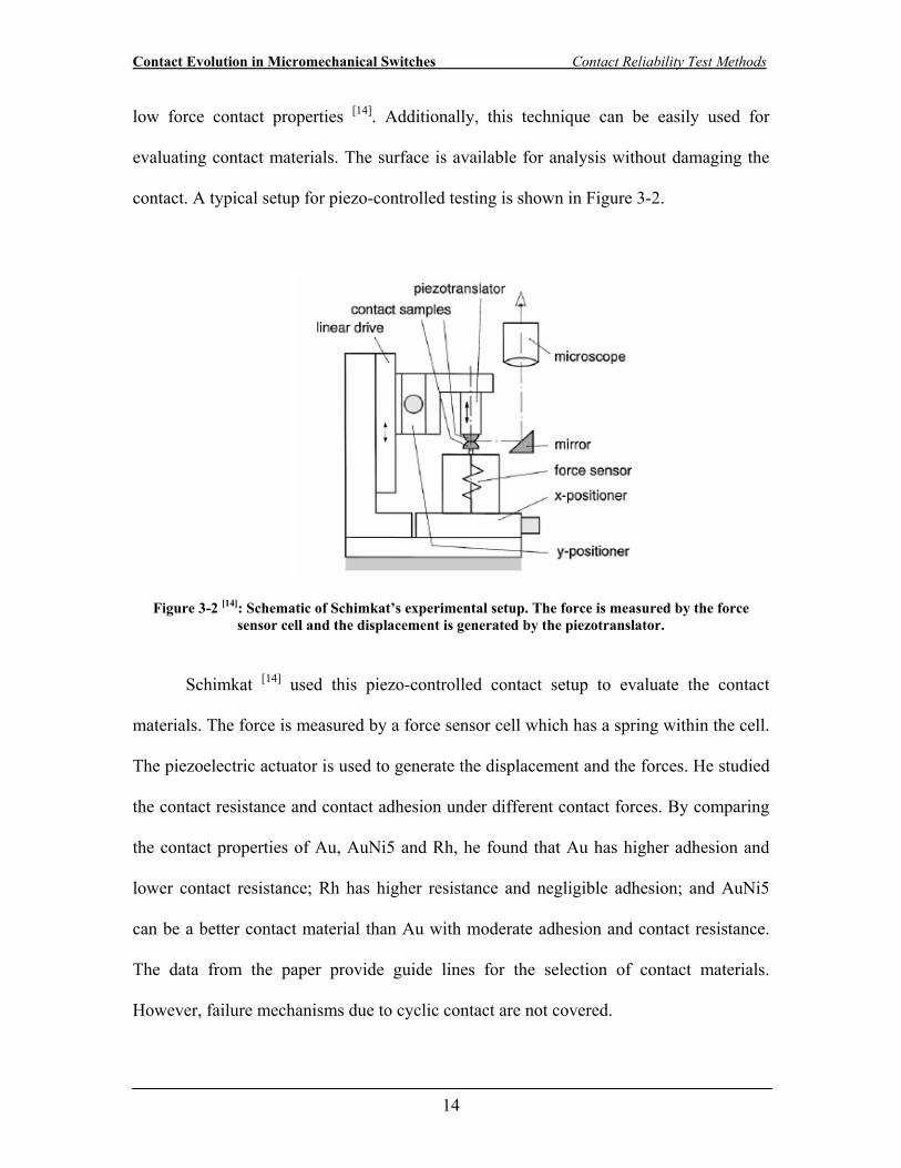
contact. A typical setup for piezo-controlled testing is shown in Figure 3-2.
Figure 3-2 [14]: Schematic of Schimkat’s experimental setup. The force is measured by the force sensor cell and the displacement is generated by the piezotranslator.
Schimkat [14] used this piezo-controlled contact setup to evaluate the contact
materials. The force is measured by a force sensor cell which has a spring within the cell.
The piezoelectric actuator is used to generate the displacement and the forces. He studied
the contact resistance and contact adhesion under different contact forces. By comparing
the contact properties of Au, AuNi5 and Rh, he found that Au has higher adhesion and
lower contact resistance; Rh has higher resistance and negligible adhesion; and AuNi5
can be a better contact material than Au with moderate adhesion and contact resistance.
The data from the paper provide guide lines for the selection of contact materials.
However, failure mechanisms due to cyclic contact are not covered.
Contact Evolution in Micromechanical Switches Contact Reliability Test Methods
15
Hyman [12] used a piezo-controlled apparatus to study gold-on-gold contacts. A
leaf spring was used to detect the force. He studied gold contact properties by using a
planar plated gold contacting gold coated tungsten probes. The radius of the tungsten
probes were several micrometers. By varying probe electrode morphology, contact force
(100-500µN) and DC current (0.1~200mA), he found that the thermal effect is the
dominant factor for the failure of the gold-on-gold contacts. The current heating and
current annealing can weld the contacts together, which causes material transfer during
the separation of the contact. The material transfer is observed when the contact force is
200µN and the current is 10mA. The material transfer is “unilaterally” increased with the
contact current. Hyman’s work demonstrates the deterioration caused by current heating
on Au/Au electrical contacts. The study suggests that a thermal sink should be designed
for the MEMS switch. However, the relation between contact force and the material
transfer is not clear.
Tringe and Uhlman [6] used an interfacial force microscope (IFM) to study single
asperity Au/Au electrical contacts at lower forces and currents. Similar to Hyman’s
method, a tungsten tip and planar plated gold contact are used for the contact test. The
radius of curvature of the tungsten tip is limited to ~800nm to satisfy the single asperity
condition. A contact event is performed by bringing the tip toward and away from the
substrate at a constant rate (4.2nm/s). The maximum loading forces are less than 35µN
and the current used for the resistance measurement is less than 1mA. During the entire
contact event the normal force and contact resistance are measured simultaneously.
Figure 3-3 shows representative IFM profiles with normal force and contact resistance
Contact Evolution in Micromechanical Switches Contact Reliability Test Methods
16
plotted as a function of relative displacement between the tip and substrate. The contact
tests are performed under different conditions: dry nitrogen, ozonation and UHV.
For the contact tests in the dry nitrogen, contact adhesion is barely detected, and
the measured resistances vary from 10 to 104Ω. The contact tests are also performed
right after exposure to ozone for 40min. After the ozonation, the contact adhesion is still
weak, but the contact resistances are reduced. The “minimum contact average
resistances” are less than 10Ω, which are still larger than the constriction resistances of
metallic contacts. Tringe and Uhlman attribute these contact characteristics to the
contamination layer on top of the metal surfaces. This contamination layer is conductive
and can not be removed by the ozonation. The ozone treatment can stabilize the electrical
performance of the contamination film and reduce the contact resistance “by more than 3
orders of magnitude”. By using X-ray photoelectron spectroscopy and time-of-flight
secondary ion mass spectrometry, they found that the contamination layer consists mostly
of hydrocarbons and the thickness of the film is about 4-6nm. The film remains relatively
stable in both composition and thickness following ozonation.
When the electrical contacts are tested under UHV conditions, the contact
properties are different than in dry nitrogen. Strong attractive forces are observed during
the contact events, and these are due to the large surface energy of the clean gold
surfaces. “Jump into contact” is observed when the tip moves toward the substrate.
During the withdrawal process, the attractive force flattens as the contacting materials
plastically flows and the contact resistance begins to slowly rise. As the tip continues to
move away the tip, the attractive force suddenly drops by about 70% percent,
accompanied by a jump of the contact resistance (as shown in Figure 3-3). The author
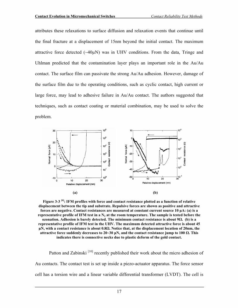
Contact Evolution in Micromechanical Switches Contact Reliability Test Methods
17
attributes these relaxations to surface diffusion and relaxation events that continue until
the final fracture at a displacement of 15nm beyond the initial contact. The maximum
attractive force detected (~40µN) was in UHV conditions. From the data, Tringe and
Uhlman predicted that the contamination layer plays an important role in the Au/Au
contact. The surface film can passivate the strong Au/Au adhesion. However, damage of
the surface film due to the operating conditions, such as cyclic contact, high current or
large force, may lead to adhesive failure in Au/Au contact. The authors suggested that
techniques, such as contact coating or material combination, may be used to solve the
problem.
(a) (b)
Figure 3-3 [6]: IFM profiles with force and contact resistance plotted as a function of relative displacement between the tip and substrate. Repulsive forces are shown as positive and attractive forces are negative. Contact resistances are measured at constant current source 10 μA: (a) is a
representative profile of IFM test in a N2 at the room temperature. The sample is tested before the ozonation. Adhesion is barely detected. The minimum contact resistance is about 9Ω. (b) is a
representative profile of IFM test in the UHV. The maximum detected attractive force is about 45 μN, with a contact resistance is about 0.8Ω. Notice that, at the displacement location of 20nm, the attractive force suddenly decreases to 20~30 μN, and the contact resistance jump to 100 Ω. This
indicates there is connective necks due to plastic deform of the gold contact.
Patton and Zabinski [10] recently published their work about the micro adhesion of
Au contacts. The contact test is set up inside a piezo-actuator apparatus. The force sensor
cell has a torsion wire and a linear variable differential transformer (LVDT). The cell is
Contact Evolution in Micromechanical Switches Contact Reliability Test Methods
18
the non-contact type with no contact between the moving magnetic core and the
windings. Gold thin films are coated on the indenter ball and a flat GaAs surface. The
cyclic test is performed by the piezoelectric actuator mounted on the ball holder, and the
cycling rate is 5Hz. All the tests are done in a well defined air environment. They studied
the effects of different currents on contact adhesion. They found that a large adhesion is
detected at low currents (1-10µA). However, when the contact current is high (1-10mA),
there is a formation of “nanowires”. The presence of the “nanowires” will roughen the
contact area and lower the contact adhesion. The observation verified the current effects
on the gold contact damage, but the author failed to give a good explanation of the
nanowire formation mechanism. Contact creep is also observed by monitoring the contact
resistance variation under the constant load. They observe contact creep at low currents.
With a loading force of about 200µN, the total force relaxation can be 60 µN due to the
creep. However, at high currents, the contact creep effect can be overridden by melting or
material transfer.
Generally, gold-on-gold contacts do not show much evidence of the degradation
of the contact resistance. Dickrell and Dugger [20] studied the contact resistance evolution
by using a Au-Pt material pair. A nano-indenter system was used to set-up the contact
test, contact materials were coated on the indenter ball and a flat surface. They monitored
the resistance degradation from cycle 1 to cycle 225, and the contact force was controlled
at 150µN. They found that the resistance degradation is strongly affected by the current
and the environment. Hot switching can accelerate the resistance degradation. Micro-arcs
at very small surface gaps may be the dominant effect for the resistance degradation.
Contact Evolution in Micromechanical Switches Contact Reliability Test Methods
19
The piezoelectric controlled contact testing method provides a straightforward
method for contact physics study. The relative limitations of these kinds of contact tests
are the limited contact geometry and the low cycling rate. The available contact shape is
usually limited by the probes and the indenter profile. The cycling rate is also limited by
the stiffness of the spring and the response time of the position sensor. Contact study is
generally limited to a stationary contact or at a low number of cycles (<1000 cycles). In
order to understand the evolution characteristics of the contact physics, the experimental
setup needs to be improved.
3.3 Challenges of Contact Study
Ever since the advent of MEMS switches, the study of contact physics at micro
and nano scales has attracted attention. Different failure modes, such as stiction and
contamination have been observed. The effects of the current, the contact force and
surface films on single contact performance have been studied. Knowledge of stationary
contact physics provides a guideline for MEMS switch design. However, the physical
failure mechanism in life time tests has not been studied in-depth. For instance, the gold-
on-gold contacts are observed to be susceptible to adhesive failure. During a cyclic test,
the contact adherence increases and contact resistance decreases. The increase of the
adhesion is believed to cause the “stiction” failure in the gold-contact switch. But, how
contacts evolve to the “stiction” failure is not known.
Contact Evolution in Micromechanical Switches Contact Reliability Test Methods
20
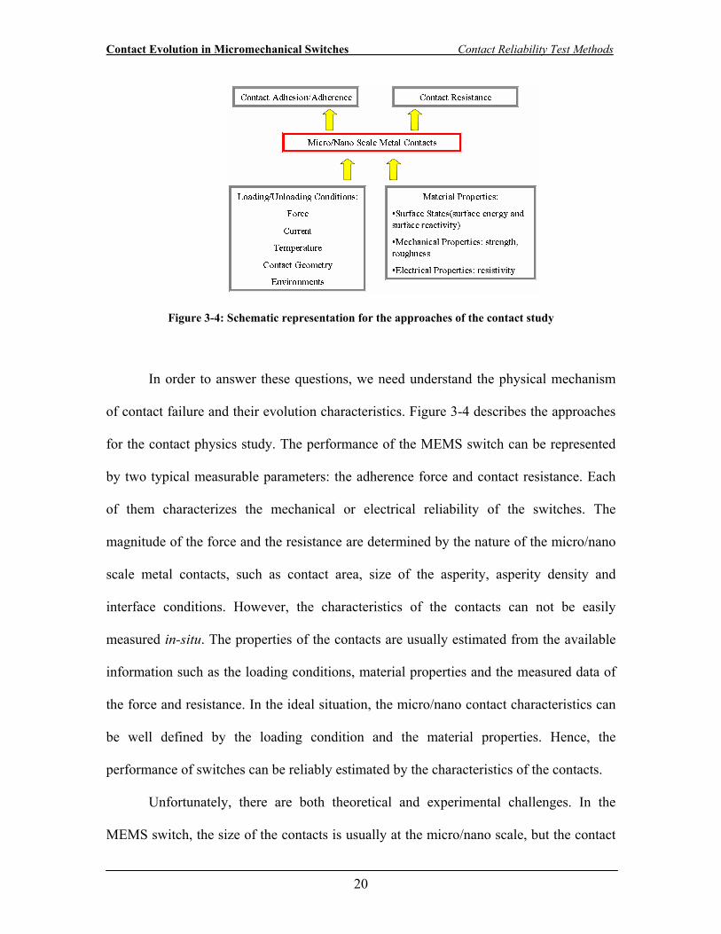
Figure 3-4: Schematic representation for the approaches of the contact study
In order to answer these questions, we need understand the physical mechanism
of contact failure and their evolution characteristics. Figure 3-4 describes the approaches
for the contact physics study. The performance of the MEMS switch can be represented
by two typical measurable parameters: the adherence force and contact resistance. Each
of them characterizes the mechanical or electrical reliability of the switches. The
magnitude of the force and the resistance are determined by the nature of the micro/nano
scale metal contacts, such as contact area, size of the asperity, asperity density and
interface conditions. However, the characteristics of the contacts can not be easily
measured in-situ. The properties of the contacts are usually estimated from the available
information such as the loading conditions, material properties and the measured data of
the force and resistance. In the ideal situation, the micro/nano contact characteristics can
be well defined by the loading condition and the material properties. Hence, the
performance of switches can be reliably estimated by the characteristics of the contacts.
Unfortunately, there are both theoretical and experimental challenges. In the
MEMS switch, the size of the contacts is usually at the micro/nano scale, but the contact
Contact Evolution in Micromechanical Switches Contact Reliability Test Methods
21
theory at this scale is not ready yet. For example, nano-scale plasticity and nano scale
current heating are still under intense investigation. How to build bridge between the
theories at the atomic-scale and the macro-scale is a hot topic in the mechanics of
materials. Due to the lack of effective contact models, the designer has to make some
assumptions which may or may not be valid. Additionally, experimental measurements of
the material properties are not straightforward. For example, the surface energy of the
contact material is strongly related to the environmental conditions. The measurement of
the surface properties usually results in data with a large scatter. It is hard to get direct in-
situ measurement of surface energy and surface hardness during the cyclic test.
Even with good theoretical models and reliable measurements, the investigation
of the failure mechanism is still challenging. Micro/nano contact characteristics are
affected by factors such as the surface energy, the hardness and the elastic modulus of the
contacts, the normal and tangential loads, the strain hardening, the time over which creep
is allowed to occur and the temperature of asperities which are in contact at the interface.
Many of these factors are interrelated and all these factors are important for contact
reliability. It is hard to design an experiment to isolate one or two factors for
investigation.
3.4 SPM for Contact Study
The object of this work is to understand the failure mechanisms of MEMS
switches and the physical basis of contact evolution. To reach this goal, I have studied the
failure mechanisms from the intrinsic properties of the contact materials and using SPM
(Scanning Probe Microscopy) for the experimental investigation.
Contact Evolution in Micromechanical Switches Contact Reliability Test Methods
22
In order to study contact evolution, the experimental setup should provide enough
flexibility for contact study. A good contact testing setup should provide accurate
measurements of the force and resistance, good control of the displacement and easy
access to the contact surfaces. The setup should be able to perform high speed cycling
tests and real time monitoring. Thus, device testing is excluded from this project. The
piezo-control testing methods can provide good force-displacement control and
measurement. However, previous piezo-controlled setups were based on a spring or a
commercial force sensor cell. The stiffness of the spring and the response speed of the
position sensor limit the cycling rate to no more than 100Hz. At the same time, the
surface morphology of the setup rely on either available probe tips or the indenter profile,
which is different from the real contact geometries in the MEMS switches.
Considering the limitations of previous experimental setups, we designed a
contact test station based on SPM. The advantage of using SPM for the contact study is
that it can provide us more flexibility to design the contact test. The SPM is originally
designed for study of surfaces. The SPM stage can provide displacement control with
subnanometer precision. The microscopy functions in the SPM, such as AFM (atomic
force microscopy), STM (scanning tunneling force microcopy) and FFM (frictional force
microscopy), can be used to study the surface roughness, surface energy and surface
films on the contact surface.
The most significant difference between the SPM setup and previous piezo-
control setups is the force measurement mechanism. The previous piezo-control setups
used a force sensor cell in which both the spring and position sensor are integrated inside
of the cell, and the contact tip is attached to the force sensor. The contact test then suffers
Contact Evolution in Micromechanical Switches Contact Reliability Test Methods
23
from the limited stiffness of the spring and the available profile of the contact bumps, and
neither of them is flexible to change. However, in the SPM system, the spring and the
position sensor are physically separated. The spring is implemented by a cantilever and a
laser lever system is used as a position sensor.
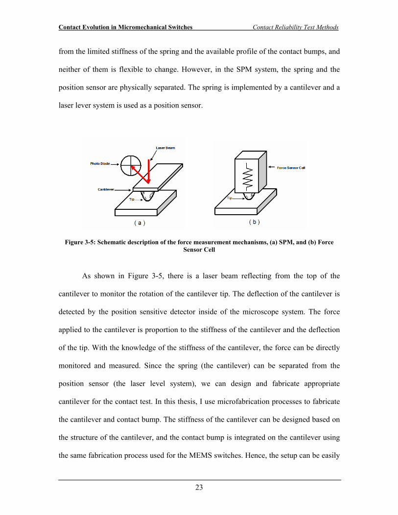
Figure 3-5: Schematic description of the force measurement mechanisms, (a) SPM, and (b) Force Sensor Cell
As shown in Figure 3-5, there is a laser beam reflecting from the top of the
cantilever to monitor the rotation of the cantilever tip. The deflection of the cantilever is
detected by the position sensitive detector inside of the microscope system. The force
applied to the cantilever is proportion to the stiffness of the cantilever and the deflection
of the tip. With the knowledge of the stiffness of the cantilever, the force can be directly
monitored and measured. Since the spring (the cantilever) can be separated from the
position sensor (the laser level system), we can design and fabricate appropriate
cantilever for the contact test. In this thesis, I use microfabrication processes to fabricate
the cantilever and contact bump. The stiffness of the cantilever can be designed based on
the structure of the cantilever, and the contact bump is integrated on the cantilever using
the same fabrication process used for the MEMS switches. Hence, the setup can be easily
Contact Evolution in Micromechanical Switches Contact Reliability Test Methods
24
used to evaluate the contact geometry and surface morphology effects on the real switch
contacts. Since the force can be measured without physically touching the cantilever, a
high speed piezoelectric actuator can be used for the contact test. We can perform real-
time measurements during the cycling test. The details of the experimental setup will be
described in the next section.
Contact Evolution in Micromechanical Switches SPM Based Contact Test System
25
4 SPM Based Contact Test System
In this chapter, the set up of the SPM based contact tester and its operational
principle is introduced. The fabrication process for a test cantilever and contact bump is
given, as well as the principles and procedures used for contact sliding and environment
control.
4.1 Setup of the Contact Station
A contact tester was set up inside a JSPM-5200 Scanning Probe Microscope (SPM)
system. The contact was made by pressing a cantilever with a contact bump onto a flat
substrate using a piezoelectric actuator (Physik Instrumente model PL022) which was
mounted on the SPM stage. The stage was used to move the substrate to the testing
position with subnanometer scale accuracy. The piezoelectric actuator was then used to
perform the contact test. The test cantilevers that were fabricated are relatively stiff when
compared to conventional AFM cantilevers. These were designed to obtain a large
contact force (0.1-1mN) during cyclic loading. Contact bumps having different shapes
were fabricated on the bottom of the cantilevers using silicon micromachining processes.
A metal deposition step following the fabrication of the bump and the substrate was used
to evaluate the performance of various contact materials.
A schematic of the experimental apparatus is shown in Figure 4-1. It is noted that
the piezoelectric actuator was mounted on a wedge with 12° slope. This was done to
ensure the test cantilever was parallel to the sample substrate because the cantilever
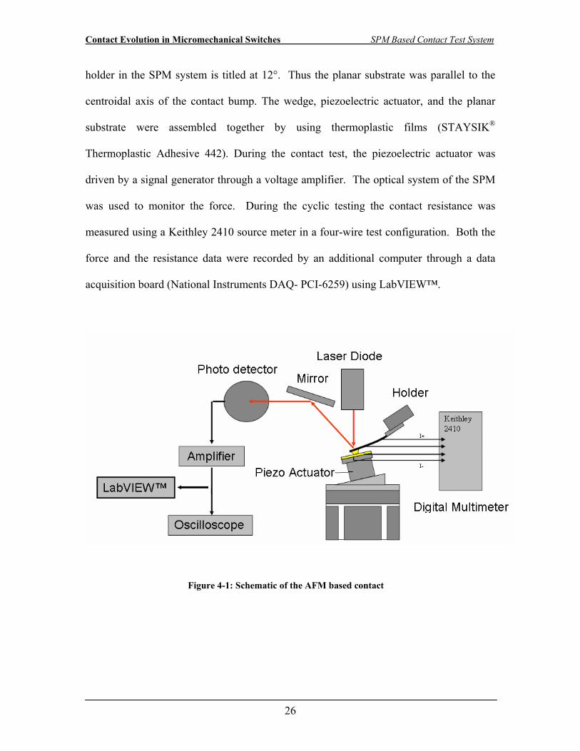
Contact Evolution in Micromechanical Switches SPM Based Contact Test System
26
holder in the SPM system is titled at 12°. Thus the planar substrate was parallel to the
centroidal axis of the contact bump. The wedge, piezoelectric actuator, and the planar
substrate were assembled together by using thermoplastic films (STAYSIK®
Thermoplastic Adhesive 442). During the contact test, the piezoelectric actuator was
driven by a signal generator through a voltage amplifier. The optical system of the SPM
was used to monitor the force. During the cyclic testing the contact resistance was
measured using a Keithley 2410 source meter in a four-wire test configuration. Both the
force and the resistance data were recorded by an additional computer through a data
acquisition board (National Instruments DAQ- PCI-6259) using LabVIEW™.
Figure 4-1: Schematic of the AFM based contact
Contact Evolution in Micromechanical Switches SPM Based Contact Test System
27
4.2 Operation Principle
The focus of this contact study is the interaction between a planar surface and a
microfabricated bump. The bump was located at the end of a microfabricated cantilever
beam. The actuation was done with the planar surface by its attached piezoelectric
actuator. Thus, when driving the piezoelectric actuator the planar surface moves up and
down and makes contact during some portion of an actuation cycle. The displacement of
the piezoelectric actuator Zp is controlled by a driving signal. The approaching of the
planar surface can cause a deflection Zc at the end of the cantilever. For the interaction
between two infinitely hard surfaces, the piezo displacement Zp is equal to the deflection
of the cantilever Zc. Since the force between two interacting surfaces Fc is proportional to
the deflection Zc, (i.e. hooke’s law ccc ZkF ⋅= for a cantilever with stiffness kc), by
monitoring the deflection during the approach, the contact force can be measured. In the
SPM system, the deflection of the cantilever is detected by an optical lever system.
Therefore within our SPM based contact tester, by adjusting the driving signal for
piezoelectric actuator Zp, the contact force can be controlled and measured by monitoring
the deflection of the cantilever Zc.
To monitor the deflection, a laser beam is focused on the end of the cantilever and
the reflected beam is detected by a position sensitive photo detector (PSPD). The
deflection of the cantilever causes a rotation at the location of the laser spot on the beam.
This in turn causes a movement of the laser spot on the PSPD. For a cantilever with
length L, the shift of the laser spot on the PSPD PDΔ is proportional to the deflection (Zc),
this relation is given by
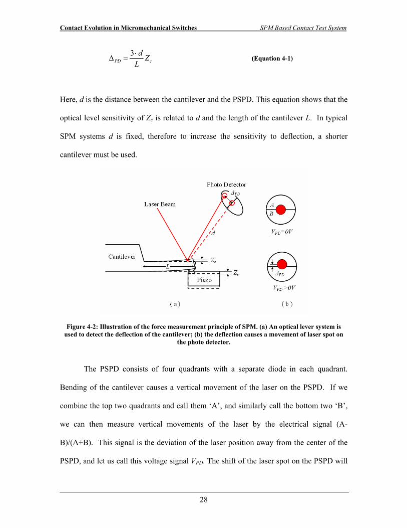
Contact Evolution in Micromechanical Switches SPM Based Contact Test System
28
cPD ZLd⋅
=Δ3
(Equation 4-1)
Here, d is the distance between the cantilever and the PSPD. This equation shows that the
optical level sensitivity of Zc is related to d and the length of the cantilever L. In typical
SPM systems d is fixed, therefore to increase the sensitivity to deflection, a shorter
cantilever must be used.
Figure 4-2: Illustration of the force measurement principle of SPM. (a) An optical lever system is used to detect the deflection of the cantilever; (b) the deflection causes a movement of laser spot on
the photo detector.
The PSPD consists of four quadrants with a separate diode in each quadrant.
Bending of the cantilever causes a vertical movement of the laser on the PSPD. If we
combine the top two quadrants and call them ‘A’, and similarly call the bottom two ‘B’,
we can then measure vertical movements of the laser by the electrical signal (A-
B)/(A+B). This signal is the deviation of the laser position away from the center of the
PSPD, and let us call this voltage signal VPD. The shift of the laser spot on the PSPD will
Contact Evolution in Micromechanical Switches SPM Based Contact Test System
29
cause the current density to change in each photo diode, therefore changing the output
voltage VPD. For a certain range of test cantilever displacements the change of output
voltage (ΔVPD) is linearly related to the change of the deflection (∆Zc), and their ratio is
represented as optical level sensitivity (S=∆VPD/∆Zc). This value can be calibrated by
using uncoated silicon cantilever and silicon substrate while performing a force-
displacement-curve (F/d) test in SPM. Assume ΔZp=ΔZc during the calibration F/d test.
After the calibration, we can use the sensitivity value S and evaluate the deflection of the
cantilever during our contact test (Zc= ΔVPD/S). For our tested cantilevers, S=50nm/V.
Per the experimental setup, the minimum detected deflection Zc was 1nm with a
0.02V minimum resolution of the voltage (ΔVPD). For the stiffness of cantilever
kc=104N/m, the minimum detectable force is 10µN. In our contact test, the output voltage
from the PSPD was recorded during the cycling test, and the value was then transferred to
the force value, according to the value of the optical lever sensitivity and the cantilever
stiffness.
4.3 Contact Cantilever and Fabrication
In our SPM based contact tester, the testing cantilever was used both as a spring
for the contact test as well as a sensor for the force measurement. Therefore, the stiffness
and the length of the cantilever determine the operation range as well as the detection
resolution of the force. In this work, the length of the cantilever was chosen as 180µm,
which will lead to an optical level sensitivity of 50nm/V. The designed stiffness was then
adjusted by choosing different thickness as well as varying the cross section of the test
cantilever.
Contact Evolution in Micromechanical Switches SPM Based Contact Test System
30
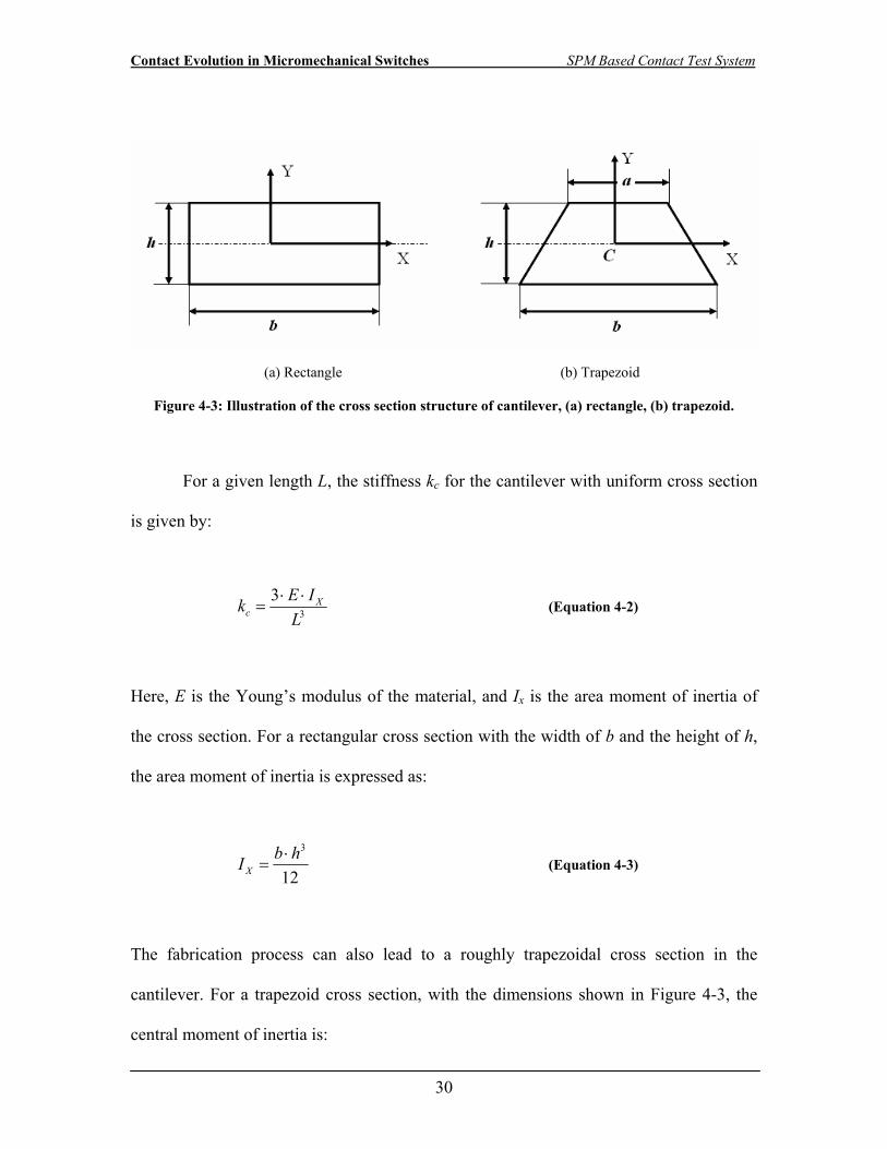
(a) Rectangle (b) Trapezoid
Figure 4-3: Illustration of the cross section structure of cantilever, (a) rectangle, (b) trapezoid.
For a given length L, the stiffness kc for the cantilever with uniform cross section
is given by:
3
3 Xc
E IkL
⋅ ⋅= (Equation 4-2)
Here, E is the Young’s modulus of the material, and Ix is the area moment of inertia of
the cross section. For a rectangular cross section with the width of b and the height of h,
the area moment of inertia is expressed as:
3
12Xb hI ⋅
= (Equation 4-3)
The fabrication process can also lead to a roughly trapezoidal cross section in the
cantilever. For a trapezoid cross section, with the dimensions shown in Figure 4-3, the
central moment of inertia is:
Contact Evolution in Micromechanical Switches SPM Based Contact Test System
31
3 2 2( 4 )36 ( )X
h a a b bIa b
+ ⋅ ⋅ +=
⋅ + (Equation 4-4)
In this work, the customized cantilever was designed for testing forces in the
range of 100μN ~5mN, which corresponds to a typical force operation range for MEMS
switches. The deflection detection range in the SPM is limited by the linear deflection
operation range of the PSPD to no more than 500nm. To get a contact force of 1mN with
a deflection of 100nm, the stiffness of the cantilever is required to be 104N/m. Using
these design criteria, the dimensions of the cantilever were chosen as 80×30×180μm.
Silicon was chosen as the material for the cantilever because it is commonly used in
microfabrication. Given a Young’s modulus of Silicon to be 150GPa, the resultant
stiffness of the test cantilever can be calculated to be 1.48x10⁴N/m for the case of a
rectangular cross section.
For the fabrication of the test cantilevers, a Silicon on Insulator (SOI) wafer
process was used. The SOI had the dimensions of a 30µm thick device layer, 2 µm thick
buried oxidized which was attached to a 350µm thick handle wafer. Figure 4-4 shows
the process flow chart. The base of the cantilever is first made from the handle part of the
SOI wafer; this was etched by Tetramethylammonium Hydroxide (TMAH) at 90 ºC for
15 hours. The 2 µm thick oxide layer served as an etch stop for this process step. The
oxide layer was then removed by using buffed oxide etch (BOE 10:1). The contact bump
was then fabricated on top of the device layer.
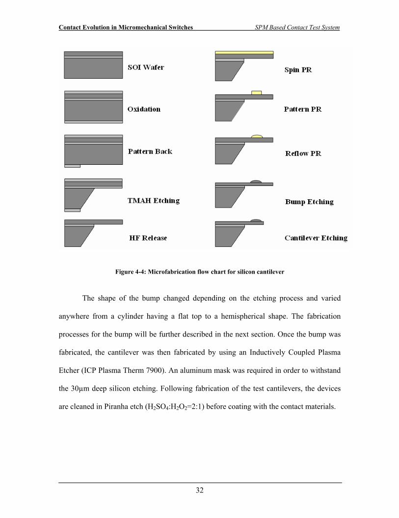
Contact Evolution in Micromechanical Switches SPM Based Contact Test System
32
Figure 4-4: Microfabrication flow chart for silicon cantilever
The shape of the bump changed depending on the etching process and varied
anywhere from a cylinder having a flat top to a hemispherical shape. The fabrication
processes for the bump will be further described in the next section. Once the bump was
fabricated, the cantilever was then fabricated by using an Inductively Coupled Plasma
Etcher (ICP Plasma Therm 7900). An aluminum mask was required in order to withstand
the 30µm deep silicon etching. Following fabrication of the test cantilevers, the devices
are cleaned in Piranha etch (H2SO4:H2O2=2:1) before coating with the contact materials.
Contact Evolution in Micromechanical Switches SPM Based Contact Test System
33
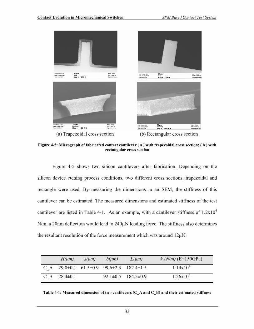
(a) Trapezoidal cross section (b) Rectangular cross section
Figure 4-5: Micrograph of fabricated contact cantilever ( a ) with trapezoidal cross section; ( b ) with
rectangular cross section
Figure 4-5 shows two silicon cantilevers after fabrication. Depending on the
silicon device etching process conditions, two different cross sections, trapezoidal and
rectangle were used. By measuring the dimensions in an SEM, the stiffness of this
cantilever can be estimated. The measured dimensions and estimated stiffness of the test
cantilever are listed in Table 4-1. As an example, with a cantilever stiffness of 1.2x10⁴
N/m, a 20nm deflection would lead to 240µN loading force. The stiffness also determines
the resultant resolution of the force measurement which was around 12µN.
H(μm) a(μm) b(μm) L(μm) kc(N/m) (E=150GPa)
C_A 29.0±0.1 61.5±0.9 99.6±2.3 182.4±1.5 1.19x10⁴
C_B 28.4±0.1 92.1±0.5 184.5±0.9 1.26x10⁴
Table 4-1: Measured dimension of two cantilevers (C_A and C_B) and their estimated stiffness
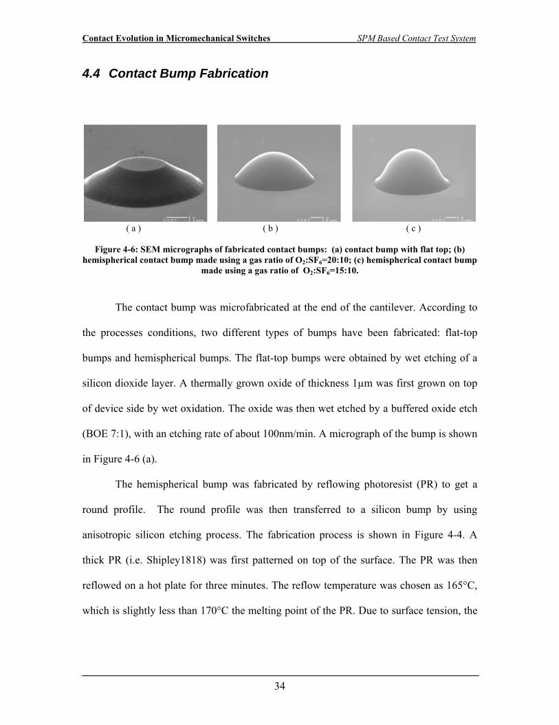
Contact Evolution in Micromechanical Switches SPM Based Contact Test System
34
4.4 Contact Bump Fabrication
( a ) ( b ) ( c )
Figure 4-6: SEM micrographs of fabricated contact bumps: (a) contact bump with flat top; (b) hemispherical contact bump made using a gas ratio of O2:SF6=20:10; (c) hemispherical contact bump
made using a gas ratio of O2:SF6=15:10.
The contact bump was microfabricated at the end of the cantilever. According to
the processes conditions, two different types of bumps have been fabricated: flat-top
bumps and hemispherical bumps. The flat-top bumps were obtained by wet etching of a
silicon dioxide layer. A thermally grown oxide of thickness 1µm was first grown on top
of device side by wet oxidation. The oxide was then wet etched by a buffered oxide etch
(BOE 7:1), with an etching rate of about 100nm/min. A micrograph of the bump is shown
in Figure 4-6 (a).
The hemispherical bump was fabricated by reflowing photoresist (PR) to get a
round profile. The round profile was then transferred to a silicon bump by using
anisotropic silicon etching process. The fabrication process is shown in Figure 4-4. A
thick PR (i.e. Shipley1818) was first patterned on top of the surface. The PR was then
reflowed on a hot plate for three minutes. The reflow temperature was chosen as 165°C,
which is slightly less than 170°C the melting point of the PR. Due to surface tension, the
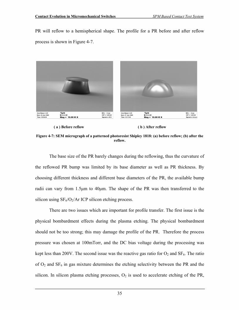
Contact Evolution in Micromechanical Switches SPM Based Contact Test System
35
PR will reflow to a hemispherical shape. The profile for a PR before and after reflow
process is shown in Figure 4-7.
( a ) Before reflow ( b ) After reflow
Figure 4-7: SEM micrograph of a patterned photoresist Shipley 1818: (a) before reflow; (b) after the reflow.
The base size of the PR barely changes during the reflowing, thus the curvature of
the reflowed PR bump was limited by its base diameter as well as PR thickness. By
choosing different thickness and different base diameters of the PR, the available bump
radii can vary from 1.5μm to 40μm. The shape of the PR was then transferred to the
silicon using SF6/O2/Ar ICP silicon etching process.
There are two issues which are important for profile transfer. The first issue is the
physical bombardment effects during the plasma etching. The physical bombardment
should not be too strong; this may damage the profile of the PR. Therefore the process
pressure was chosen at 100mTorr, and the DC bias voltage during the processing was
kept less than 200V. The second issue was the reactive gas ratio for O2 and SF6. The ratio
of O2 and SF6 in gas mixture determines the etching selectivity between the PR and the
silicon. In silicon plasma etching processes, O2 is used to accelerate etching of the PR,
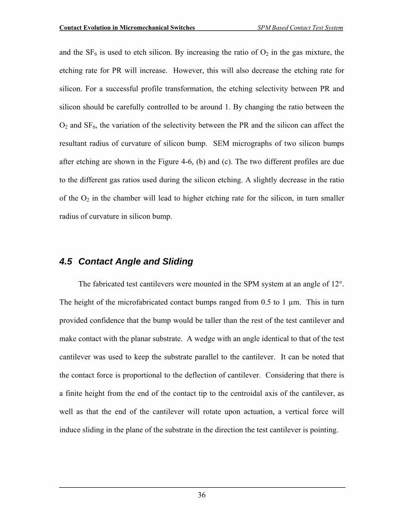
Contact Evolution in Micromechanical Switches SPM Based Contact Test System
36
and the SF6 is used to etch silicon. By increasing the ratio of O2 in the gas mixture, the
etching rate for PR will increase. However, this will also decrease the etching rate for
silicon. For a successful profile transformation, the etching selectivity between PR and
silicon should be carefully controlled to be around 1. By changing the ratio between the
O2 and SF6, the variation of the selectivity between the PR and the silicon can affect the
resultant radius of curvature of silicon bump. SEM micrographs of two silicon bumps
after etching are shown in the Figure 4-6, (b) and (c). The two different profiles are due
to the different gas ratios used during the silicon etching. A slightly decrease in the ratio
of the O2 in the chamber will lead to higher etching rate for the silicon, in turn smaller
radius of curvature in silicon bump.
4.5 Contact Angle and Sliding
The fabricated test cantilevers were mounted in the SPM system at an angle of 12°.
The height of the microfabricated contact bumps ranged from 0.5 to 1 µm. This in turn
provided confidence that the bump would be taller than the rest of the test cantilever and
make contact with the planar substrate. A wedge with an angle identical to that of the test
cantilever was used to keep the substrate parallel to the cantilever. It can be noted that
the contact force is proportional to the deflection of cantilever. Considering that there is
a finite height from the end of the contact tip to the centroidal axis of the cantilever, as
well as that the end of the cantilever will rotate upon actuation, a vertical force will
induce sliding in the plane of the substrate in the direction the test cantilever is pointing.
Contact Evolution in Micromechanical Switches SPM Based Contact Test System
37
Figure 4-8: Contact angle set-up for cyclic test. Wedge is used to keep the planar substrate parallel to the cantilever.
Assume a force P is applied in the Z direction to the end of the cantilever. The
angle θΔ and the displacement ZΔ at the end of the cantilever can be expressed as:
2
2P L
E Iθ ⋅
Δ =⋅ ⋅
(Equation 4-5)
3
3P LZ
E I⋅
Δ =⋅ ⋅
(Equation 4-6)
where L is the length of the cantilever, E is the material parameter Young’s Modulus and
I is the second moment of the area of the cross section. It can also be noted that the
corresponding horizontal displacement XΔ is proportional to the deflection angle θΔ :
32
hX h ZL
θ ⋅⎛ ⎞Δ = ⋅Δ = Δ⎜ ⎟⋅⎝ ⎠ (Equation 4-7)
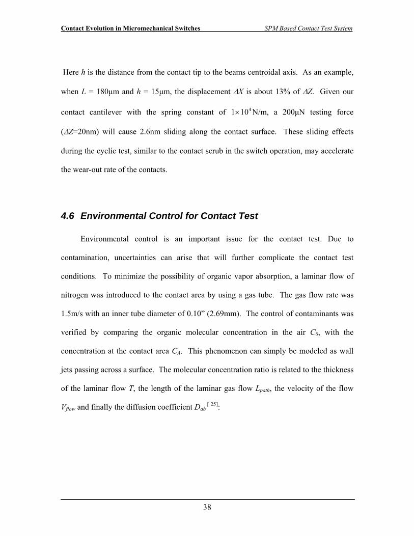
Contact Evolution in Micromechanical Switches SPM Based Contact Test System
38
Here h is the distance from the contact tip to the beams centroidal axis. As an example,
when L = 180μm and h = 15μm, the displacement ΔX is about 13% of ΔZ. Given our
contact cantilever with the spring constant of 4101× N/m, a 200μN testing force
(ΔZ=20nm) will cause 2.6nm sliding along the contact surface. These sliding effects
during the cyclic test, similar to the contact scrub in the switch operation, may accelerate
the wear-out rate of the contacts.
4.6 Environmental Control for Contact Test
Environmental control is an important issue for the contact test. Due to
contamination, uncertainties can arise that will further complicate the contact test
conditions. To minimize the possibility of organic vapor absorption, a laminar flow of
nitrogen was introduced to the contact area by using a gas tube. The gas flow rate was
1.5m/s with an inner tube diameter of 0.10” (2.69mm). The control of contaminants was
verified by comparing the organic molecular concentration in the air C0, with the
concentration at the contact area CA. This phenomenon can simply be modeled as wall
jets passing across a surface. The molecular concentration ratio is related to the thickness
of the laminar flow T, the length of the laminar gas flow Lpath, the velocity of the flow
Vflow and finally the diffusion coefficient Dab [ 25]:
Contact Evolution in Micromechanical Switches SPM Based Contact Test System
39
⎥⎥⎥⎥⎥
⎦
⎤
⎢⎢⎢⎢⎢
⎣
⎡
⋅⋅=
2/10 )4(flow
pathab
A
VL
D
TerfcCC
(Equation 4-8)
We choose the diffusion coefficient value of benzene in nitrogen for our estimation,
being Dab= 0.102 cm2sec-1 [26]. The nitrogen flow thickness was about half of the pipe
inner diameter (T=1.3mm). The distance between the tube and the test center Lpath was
about 1mm. Based on this calculation, the organic vapor concentration at the area of
contact was five orders of magnitude lower than the concentration in the air. Therefore,
by using this method the diffusion of organic molecules from the atmosphere to the
contact area was efficiently prevented.
Figure 4-9: Nitrogen flow set-up for the environmental control.
To evaluate the efficiency of the nitrogen set up, we studied the contamination
rate of ruthenium contacts with or without nitrogen flow. Ruthenium (Ru) contacts are
susceptible to the contamination problem. Detail discussion of Ru contacts will be shown
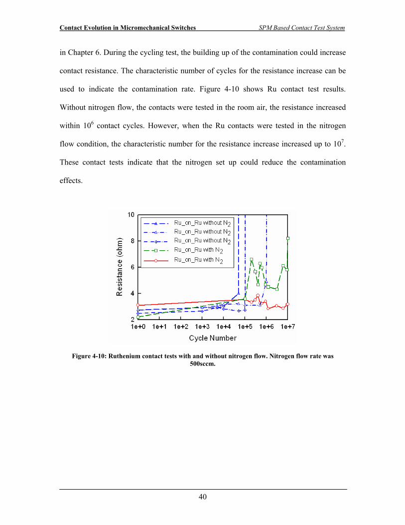
Contact Evolution in Micromechanical Switches SPM Based Contact Test System
40
in Chapter 6. During the cycling test, the building up of the contamination could increase
contact resistance. The characteristic number of cycles for the resistance increase can be
used to indicate the contamination rate. Figure 4-10 shows Ru contact test results.
Without nitrogen flow, the contacts were tested in the room air, the resistance increased
within 106 contact cycles. However, when the Ru contacts were tested in the nitrogen
flow condition, the characteristic number for the resistance increase increased up to 107.
These contact tests indicate that the nitrogen set up could reduce the contamination
effects.
Figure 4-10: Ruthenium contact tests with and without nitrogen flow. Nitrogen flow rate was 500sccm.
Contact Evolution in Micromechanical Switches Adhesive Failure in Contact Evolution
41
5 Adhesive Failure in Contact Evolution
An important reliability issue in MEMS switches is adhesive failure. This failure
is the result of a strong bond which develops between the contacts. When the contact
begins separation, this strong bonding may cause a large degree of material transfer or
even prevent the two surfaces from separating. Either of these effects can cause switch
failure. Adhesive failure has typically been observed after the switch has been operated a
certain number of cycles. Therefore, understanding the evolution of contact morphology
and its relation to adhesive failure are important.
In this work, our study is focused on the modes of separation with respect to their
role in the evolution of contact. Within this chapter, contact mechanics and separation
mechanisms are first introduced with a focus on two separation modes, brittle and ductile.
A study of the separation modes and their relation to the quasi-static and rate related pull
off force will follow and will be elaborated on by a demonstration of contact morphology
evolution. At the end of this chapter, the effects of size and material on adhesive failure
in contacts are discussed. Overall, a physical picture of the switch adhesive failure
mechanism during the evolution of gold contacts can be seen in these results.
5.1 Contact Adhesion
To begin, consider the interaction of the exposed atoms between two closed
surfaces. When two metal surfaces come into contact, attractive forces acting at edge of
the contact pull the surfaces together. These attractive forces may be caused by metallic
bonding between the two surfaces, or by van der Waals forces that act between absorbed
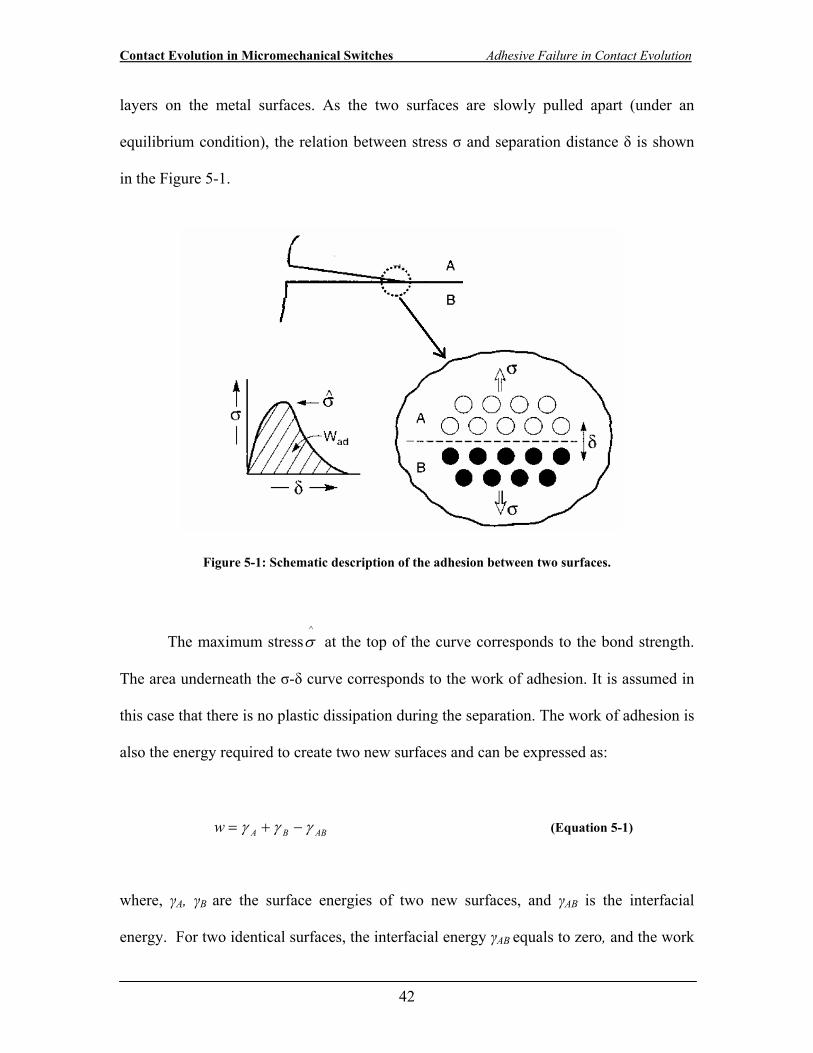
Contact Evolution in Micromechanical Switches Adhesive Failure in Contact Evolution
42
layers on the metal surfaces. As the two surfaces are slowly pulled apart (under an
equilibrium condition), the relation between stress σ and separation distance δ is shown
in the Figure 5-1.
Figure 5-1: Schematic description of the adhesion between two surfaces.
The maximum stress^σ at the top of the curve corresponds to the bond strength.
The area underneath the σ-δ curve corresponds to the work of adhesion. It is assumed in
this case that there is no plastic dissipation during the separation. The work of adhesion is
also the energy required to create two new surfaces and can be expressed as:
ABBAw γγγ −+= (Equation 5-1)
where, γA, γB are the surface energies of two new surfaces, and γAB is the interfacial
energy. For two identical surfaces, the interfacial energy γAB equals to zero, and the work
Contact Evolution in Micromechanical Switches Adhesive Failure in Contact Evolution
43
of adhesion w =2γ (γ = Aγ = Bγ ). The work of adhesion and/or surface energies can be
strongly related to the surface conditions. For example, the surface energy can change
from 1 ~ 3J/m2 for clean metal surfaces, to less than 0.1mJ/m2 for a given metal surface
with absorbed molecules [27].
Contact adhesion can be further described by the maximum attractive force acting
on the contacts. In continuum mechanics, contact adhesion can be estimated based on
contact geometry and the work of adhesion. Consider the case of an adhesive contact
between a elastic spherical bump and a planar surface. The contact adhesion Fad, can be
estimated as:
32adF wR JKRπ= (Equation 5-2)
or
2adF wR DMTπ= (Equation 5-3)
Here, R is the effective radius of the contact curvature, and w is the work of adhesion.
Notice that there are two adhesion models: Johnson-Kendall-Roberts (JKR) model [28]
and Derjaguin-Muller-Toporov (DMT) model [29]. Typically, the JKR model applies to
soft materials that have relatively large surface energies. On the other hand, the DMT
model better fits the case of hard materials that have less surface energies. The criterion
µ, introduced by Tabor [30], can be used to select which model is appropriate for a given
situation.
Contact Evolution in Micromechanical Switches Adhesive Failure in Contact Evolution
44
1/32
*2 30
R wE z
μ⎛ ⎞⋅
= ⎜ ⎟⋅⎝ ⎠ (Equation 5-4)
Here 0z is the equilibrium separation between two atomic planes and *E is the composite
Young’s modulus given by
]/)1(/)1[(1
2221
21
*
EEE
νν −+−= (Equation 5-5)
in which E1, E2 and v1, v2 are the Young’s modulus and the Poisson ratio of the sphere
and the planar surface. When µ>>1, the JKR model is valid, and when µ<<1 the DMT
better suits the contact under study. For the transition region, more comprehensive
solutions have been presented by Maugis [31] and Greenwood [32].
5.2 Separation of Adhesive Contacts
5.2.1 Two Separation Modes
In an adhesive contact, the process of loading can be related to the development
of new bonds between two surfaces. The bonding strength depends on loading force, time
in contact and surface conditions. Conversely, the process of unloading can be treated as
the fracture of these bonds. In fracture mechanics, the bond breaking procedure is
described as the propagation of a crack from the edge of the contact to the center. When
separation of the contact happens prior to any plastic deformation, the separation is called
brittle separation. For a brittle separation, the separation can happen at the original
Contact Evolution in Micromechanical Switches Adhesive Failure in Contact Evolution
45
interface, which is called “cleave”, or can happen along the grain boundaries, which is
called “intergranualr fracture”. However, with strong bonding at the interface, there may
be other separation mode can happen, that is the contact opening may happen at or near
the original interface, with absorption of energy by dislocation generation and plastic
deformation. The separation proceeds with varying degree of the plastic deformation.
Such separation mode is called ductile separation. As we will show in this work, ductile
separation could cause surface modification and material transfer, which may affect the
reliability of metal contact MEMS switch.
In general, the separation mode is strongly affected by material properties and
surface conditions. Each contact material should have an intrinsic separation mode. Yan
et al. [33] used a finite element model to study separation modes for two contact materials:
gold (Au) and ruthenium (Ru). Both contacts were assumed to have the same work of
adhesion of 1J/m2. Based upon the simulation, they found that there was a necking
phenomenon during the separation of the gold contacts, which indicates a ductile
separation. However, such necking was not observed in the separation of Ru contacts,
and the separation modes for Ru contacts are typically brittle. The different separation
modes for these two contact materials are attributed primarily to their different material
hardnesses. The Au contacts with low hardness are intrinsically ductile.
In addition, the work of adhesion can affect the separation modes. These features
were demonstrated by molecular dynamic simulations. Song and Srolorvitz [34,35]
performed 3-D molecular dynamics simulations of a Au/Au asperity contact of type Face
Centered Cubic (FCC) at 300K. The initial hemispherical asperity radius was ~3nm. The
velocity of the approach and separation was constant at 1m/s. It was found that the
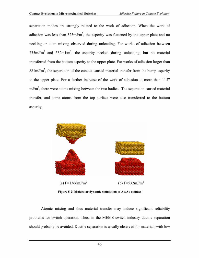
Contact Evolution in Micromechanical Switches Adhesive Failure in Contact Evolution
46
separation modes are strongly related to the work of adhesion. When the work of
adhesion was less than 523mJ/m2, the asperity was flattened by the upper plate and no
necking or atom mixing observed during unloading. For works of adhesion between
735mJ/m2 and 532mJ/m2, the asperity necked during unloading, but no material
transferred from the bottom asperity to the upper plate. For works of adhesion larger than
881mJ/m2, the separation of the contact caused material transfer from the bump asperity
to the upper plate. For a further increase of the work of adhesion to more than 1157
mJ/m2, there were atoms mixing between the two bodies. The separation caused material
transfer, and some atoms from the top surface were also transferred to the bottom
asperity.
(a) Г=1366mJ/m2 (b) Г=532mJ/m2
Figure 5-2: Molecular dynamic simulation of Au/Au contact
Atomic mixing and thus material transfer may induce significant reliability
problems for switch operation. Thus, in the MEMS switch industry ductile separation
should probably be avoided. Ductile separation is usually observed for materials with low
Contact Evolution in Micromechanical Switches Adhesive Failure in Contact Evolution
47
hardness, for example indium contacts [36] and nano scale gold-on-gold contacts [37]. It is
also seen for materials with high surface energy, for example platinum-tungsten contacts
in UHV [38]. Two factors seem to be important for ductile failure, the hardness and the
surface energy. To demonstrate these factors in their relation to the mode of separation,
we discuss physical mechanisms of both separation modes in the following two sections.
Maugis [39] (1978) has used linear elastic fracture mechanics to study elastic contact.
Similarly within this work, fracture mechanics will be used to describe contact
separation.
5.2.2 Crack Propagation and Griffith Concept
In fracture mechanics, the separation of two bodies can be characterized by the
propagation of the crack tip. At the location of a crack tip a stress singularity is generated
inside of the structure, and for the crack to propagate the energy conservation condition
must be satisfied. Griffith [40] (1920) developed an energy-balance concept to describe a
condition for the propagation of the crack tip. According to Griffith’s concept, the crack
growth is determined by the balance of the mechanical energy, UM, and the surface
energy , US. The mechanical energy includes two terms, the strain energy, which is stored
in the elastic medium, UE, as well as the potential energy due to the load, UA. The surface
energy term, US, is the free energy expended in creating new surfaces as the crack
propagates. The total energy of the system can be expressed as:
SMSAE UUUUUU +=++= (Equation 5-6)
Contact Evolution in Micromechanical Switches Adhesive Failure in Contact Evolution
48
Under the thermodynamic equilibrium condition,
0=∂∂
AU
(Equation 5-7)
Where, A is the crack interfacial area. Griffith defined a quantity called the elastic-
energy-release rate, G
dAdUG M−= (Equation 5-8)
For crack propagation in brittle mode, the elastic-energy-release rate should always
balance the energy generated from the creation of the new surfaces, or work of adhesion
w.
ABBAs
dAdUw γγγ −+== (Equation 5-9)
The energy condition for propagation of a crack tip can be defined as:
wG ≥ (Equation 5-10)
Thus the elastic-energy-release rate is always greater or equal to the work of adhesion. It
can also be seen from these expressions that plastic dissipation is not included in Griffith
concept. Therefore, the Griffith energy condition can only be used to describe brittle
Contact Evolution in Micromechanical Switches Adhesive Failure in Contact Evolution
49
separation. For ductile materials, propagation of a crack tip always comes with plastic
dissipation. Irwin [41] and Orowan [42] addressed this issue by the proposition of including
a plastic dissipation term Γp in the energy balance system. Therefore, the energy
condition for propagating a crack becomes:
PwG Γ+≥ (Equation 5-11)
Plastic dissipation usually arises from plastic deformation around the crack tip. The
magnitude of the plastic dissipation is a function of the work of adhesion w, Γp= Γp(w).
The calculation of plastic dissipation is not trivial. One reason for this is an accurate
description of plastic dissipation should include length scale effects. Models that further
describe these effects can be found in the literature of interface fracture mechanics [43,44].
5.2.3 Cleavage and Dislocation Nucleation
In this section, the origins of ductile separation are discussed. At the atomic scale,
the physical mechanism of ductile stretching can be described as dislocation nucleation
along the crystal slip plane [45]. It can be interpreted that the brittle separation is interface
cleaving, while the ductile separation is dislocation nucleation. Analogous to the surface
energy term in Griffith cleavage concept, Rice [46] introduced a new solid state property,
unstable stack energy to describe the energy dissipation associated with the ductile
separation. He then analyzed the separation mode based upon the energy cost for each
separation mode. A detailed discussion of Rice theory follows.
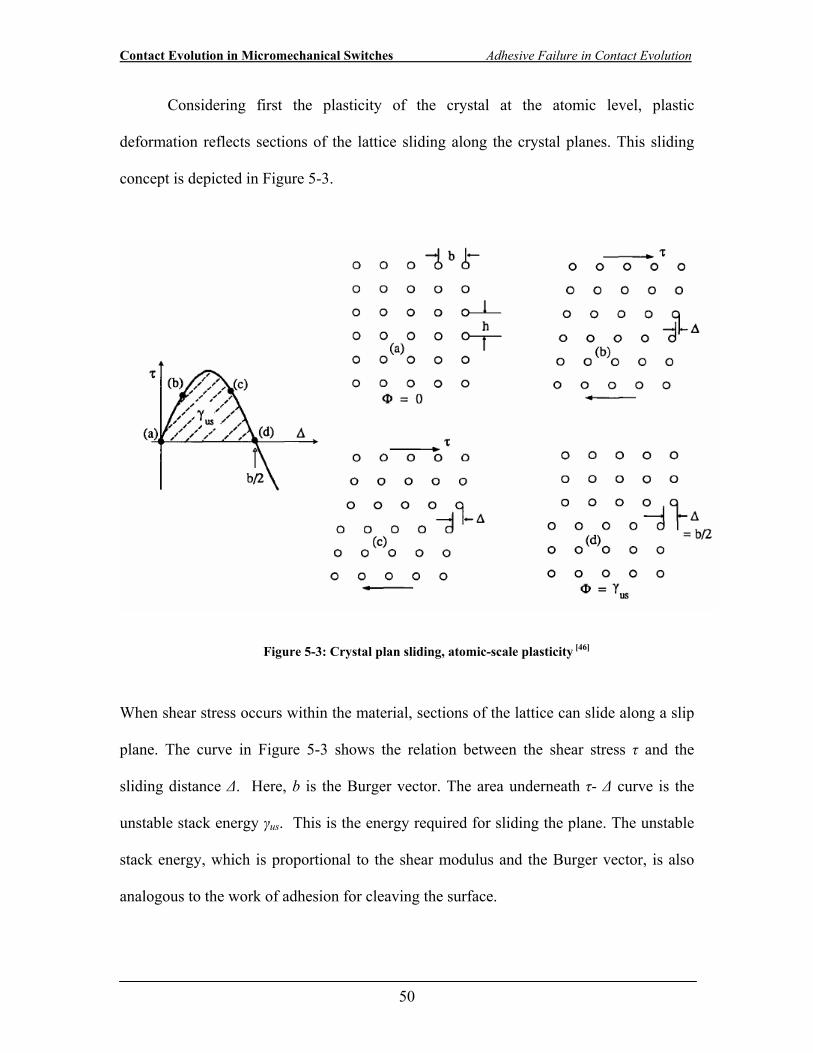
Contact Evolution in Micromechanical Switches Adhesive Failure in Contact Evolution
50
Considering first the plasticity of the crystal at the atomic level, plastic
deformation reflects sections of the lattice sliding along the crystal planes. This sliding
concept is depicted in Figure 5-3.
Figure 5-3: Crystal plan sliding, atomic-scale plasticity [46]
When shear stress occurs within the material, sections of the lattice can slide along a slip
plane. The curve in Figure 5-3 shows the relation between the shear stress τ and the
sliding distance Δ. Here, b is the Burger vector. The area underneath τ- Δ curve is the
unstable stack energy γus. This is the energy required for sliding the plane. The unstable
stack energy, which is proportional to the shear modulus and the Burger vector, is also
analogous to the work of adhesion for cleaving the surface.
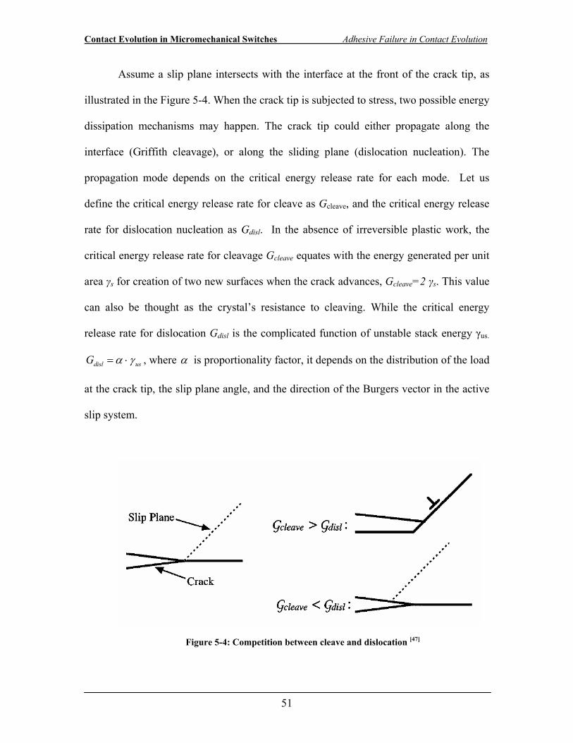
Contact Evolution in Micromechanical Switches Adhesive Failure in Contact Evolution
51
Assume a slip plane intersects with the interface at the front of the crack tip, as
illustrated in the Figure 5-4. When the crack tip is subjected to stress, two possible energy
dissipation mechanisms may happen. The crack tip could either propagate along the
interface (Griffith cleavage), or along the sliding plane (dislocation nucleation). The
propagation mode depends on the critical energy release rate for each mode. Let us
define the critical energy release rate for cleave as Gcleave, and the critical energy release
rate for dislocation nucleation as Gdisl. In the absence of irreversible plastic work, the
critical energy release rate for cleavage Gcleave equates with the energy generated per unit
area γs for creation of two new surfaces when the crack advances, Gcleave=2 γs. This value
can also be thought as the crystal’s resistance to cleaving. While the critical energy
release rate for dislocation Gdisl is the complicated function of unstable stack energy γus.
usdislG γα ⋅= , where α is proportionality factor, it depends on the distribution of the load
at the crack tip, the slip plane angle, and the direction of the Burgers vector in the active
slip system.
Figure 5-4: Competition between cleave and dislocation [47]
Contact Evolution in Micromechanical Switches Adhesive Failure in Contact Evolution
52
The separation modes are then determined by comparing two critical energy
release rate, or associated energy dissipation [47]. When Gcleave < Gdisl, the crack moves
along the cleave path and the fracture can be defined as brittle. When Gcleave >Gdisl, the
stress at the crack tip will be released by dislocation nucleation. The tip front will now
move along the slip plane, thus causing atomic level plasticity inside of the metal.
For a given material and crack plane, the value of the Gdisl can be calculated from
first principles. Rice calculated the energies for (100) cracks under mode I loading,
wherein a tensile load is normal to the crack plane. He found that the requirement for
dislocation nucleation to occur before Griffith cleavage is:
9.1( ) 6.3( )s
us
fcc or bccγγ
> (Equation 5-12)
In this calculation, the slip plane is (110) for an FCC and (111) for BCC structures. Both
required ratios are strongly reduced with a small deviation from pure mode I loading.
When the shear loading is only 10% of the tensile loading, the ratio is reduced to:
4.2( ) 3.5( )s
us
fcc or bccγγ
> (Equation 5-13)
Consider for example a Au/Au contact, based on Rice’s calculation, the unstable stack
energy is γus = 0.14 J/m2. Given the criteria in the Equation 5-13, it can be determined
that the surface energy needed for crack blunting is γs = 0.588 J/m2 with small sliding
effects. Assume the contact is between two perfect matching surfaces with zero
Contact Evolution in Micromechanical Switches Adhesive Failure in Contact Evolution
53
interfacial energy. Then the critical work of adhesion for the transition from brittle to
ductile separation for Au contacts is w = 1.17 J/m2 (w=2γs). This value is much larger
than the result of a molecular dynamics (MD) simulation from Song and Srolorvitz, who
found that the ductile to brittle transition is happening at the work of adhesion around
0.532 J/m2. The difference between the Rice model and the MD simulation could be due
to the induced shear stress for the simulation which may be greater than the 10% assumed
in Equation 5-13. The movement of the atoms could introduce the shear stress and
significantly reduce the energy needed for dislocation nucleation.
According to Rice’s theory, ductile separation is related to two intrinsic material
properties, surface energy and unstable stack energy. These two factors can be related to
two parameters in continuum mechanics, the work of adhesion and the yield strength.
Therefore, for contact materials with low hardness, it is easy to have ductile failure. For
an intrinsically ductile material, the surface cleanness can be critical factor for the
transition between the brittle and ductile cases. Take the example of gold contacts, the
surface energy of a clean gold surface is usually around 1~2J/m2. In relation to our
discussion, gold is an intrinsically ductile material. Therefore, ductile separation is
expected in Au/Au contacts as long as the surface is free of contaminants.
5.2.4 Pull Off Force
The pull off force can be defined as the maximum force required to open a
contact. Depending on the mode of separation, the magnitude of the pull off force arises
from different factors. For a purely brittle separation with no plastic dissipation during
the contact opening, the magnitude of the pull off force can be determined by knowing
Contact Evolution in Micromechanical Switches Adhesive Failure in Contact Evolution
54
the work of adhesion. For example, to separate a purely elastic sphere of radius R and a
planar surface, the pull off force is equal to the contact adhesion. This can be found from
the JKR or DMT model (Equation 5-1 and Equation 5-2). The contact area, surface
morphology, and most importantly the surface energy have strong effects on the
magnitude of this pull off force. With no plastic dissipation or viscosity effects, the
separation jump for a brittle separation can be very abrupt.
On the other hand, the magnitude of the pull off force in a ductile mode
corresponds to the ductile area and material properties. If we further assume the metal is
elastic-perfect plastic (no hardening effects), the pull off force adF is approximately equal
to the product of the material hardness, H and the ductile area A, and HAFad ⋅= . For a
gold thin film with a hardness of H =1GPa, the 70µN pull off force corresponds to a
ductile area of 0.06µm2.
5.2.5 Force Measurement
In this work, the pull off force of separation is measured by monitoring the
bending of the cantilever beam during the separation. As described in the previous
chapter, the rotation of the cantilever tip is detected by using the optical lever system in
the SPM. The maximum bending before the separation jump of the cantilever represents
the magnitude of the pull off force. The measured force-displacement curve is presented
in Figure 5-5.
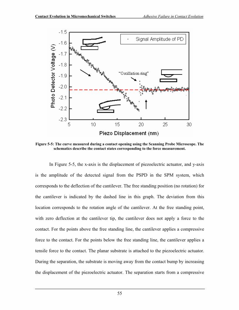
Contact Evolution in Micromechanical Switches Adhesive Failure in Contact Evolution
55
Figure 5-5: The curve measured during a contact opening using the Scanning Probe Microscope. The schematics describe the contact states corresponding to the force measurement.
In Figure 5-5, the x-axis is the displacement of piezoelectric actuator, and y-axis
is the amplitude of the detected signal from the PSPD in the SPM system, which
corresponds to the deflection of the cantilever. The free standing position (no rotation) for
the cantilever is indicated by the dashed line in this graph. The deviation from this
location corresponds to the rotation angle of the cantilever. At the free standing point,
with zero deflection at the cantilever tip, the cantilever does not apply a force to the
contact. For the points above the free standing line, the cantilever applies a compressive
force to the contact. For the points below the free standing line, the cantilever applies a
tensile force to the contact. The planar substrate is attached to the piezoelectric actuator.
During the separation, the substrate is moving away from the contact bump by increasing
the displacement of the piezoelectric actuator. The separation starts from a compressive
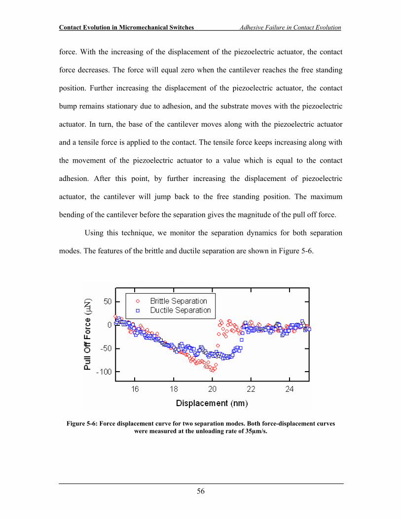
Contact Evolution in Micromechanical Switches Adhesive Failure in Contact Evolution
56
force. With the increasing of the displacement of the piezoelectric actuator, the contact
force decreases. The force will equal zero when the cantilever reaches the free standing
position. Further increasing the displacement of the piezoelectric actuator, the contact
bump remains stationary due to adhesion, and the substrate moves with the piezoelectric
actuator. In turn, the base of the cantilever moves along with the piezoelectric actuator
and a tensile force is applied to the contact. The tensile force keeps increasing along with
the movement of the piezoelectric actuator to a value which is equal to the contact
adhesion. After this point, by further increasing the displacement of piezoelectric
actuator, the cantilever will jump back to the free standing position. The maximum
bending of the cantilever before the separation gives the magnitude of the pull off force.
Using this technique, we monitor the separation dynamics for both separation
modes. The features of the brittle and ductile separation are shown in Figure 5-6.
Figure 5-6: Force displacement curve for two separation modes. Both force-displacement curves were measured at the unloading rate of 35µm/s.
Contact Evolution in Micromechanical Switches Adhesive Failure in Contact Evolution
57
In the brittle mode, the separation jump was abrupt. After the separation, an
oscillation ring is observed when the cantilever went back to free standing position. The
oscillation was naturally damped in the room air.
However, for ductile separation, due to the plastic dissipation during the contact
opening, a plateau region is observed in the force-displacement-separation curve. This
plateau region may indicate the ductile elongation during the separation. The material
could be pulled out of the surface as a ductile neck. The neck height corresponds to the
length of the plateau region. In this separation, the neck height could be 3~4nm. It is
noted that “ring” amplitude is smaller in the ductile mode than in the brittle mode. This
could be due to the smaller pull off force in this ductile separation, compared to the brittle
mode. It also could be due to the damping effect during the plastic dissipation.
It is noticed that the change of the slope in the force-displacement separation
curve could also be caused by the change of the contact area. The smaller contact area
would correspond to smaller contact stiffness, in turn resulting in a larger slope. Hence,
simply by monitoring the changing of the slope may not be enough to identify a ductile
separation. In this work, we found by monitoring rate dependent pull off force could be a
tool for detecting of the separation modes.
5.3 Rate Dependent Pull-Off Force and Separation Modes
5.3.1 Introduction
Since closing and opening a contact is a time related process, the cycling rate
could affect the magnitude of the pull off force. The rate dependent pull force should
depend on the physical mechanisms involved in the cycling process. With different
Contact Evolution in Micromechanical Switches Adhesive Failure in Contact Evolution
58
separation mechanisms, brittle mode and ductile mode could have different features for
the rate dependent pull off force. Based on this concern, we study the rate-related
properties of the pull off force and its relation to the separation mode.
For a brittle mode, the physical mechanism for contact opening is breaking bonds
along the interface. The surface events, such as interposing films, can affect the contact
opening. The rate dependent pull off force should be characterized by the surface events.
For a ductile separation, the mechanism for contact opening is associated with the lattice
planes sliding or atoms arrangement inside of the film materials. The rate dependent pull
off force should be determined by the bulk effects. The rate dependent pull off force has
not been widely studied for metal contacts. However, the rate related adhesion has been
observed in areas such as adhesion of polymer [48], and atomic scale friction forces [49].
Both studies have shown that there are distinctive rate related responses according to the
separation mode.
For instance, the polymer studies [48] have shown that, when the polymer is in the
“glassy” state, the separation is brittle. The rate related pull off force is either independent
of the rate, or decreases with increasing of the cycling rate. On the other hand, when the
polymer is in the “liquid” state, the separation is ductile. It is found that the pull off force
increases with the increasing of the unloading rate. The different rate dependent
properties are due to the different opening mechanisms. During the brittle separation, the
surface effects are dominant. With the longer resting time in contact, stronger bonding
will develop. In contrast, during the ductile separation, the bulk effects are dominant. The
bulk viscosity effects cause larger pull off force during the fast unloading.
Contact Evolution in Micromechanical Switches Adhesive Failure in Contact Evolution
59
Similar behavior is also observed in the nanoscopic frictional force study [49]. It is
shown that, for a partially hydrophilic surface with nanometer scale roughness, the
frictional force shows different rate related properties under different testing conditions.
When the experiments are performed in the ambient condition, frictional force decreases
with the increasing of the sliding velocity. However, when the same experiments are
performed under UHV condition, the opposite rate dependent properties are observed. It
is found that the decreasing slope of the frictional force in ambient condition is due to the
meniscus bridge condensation. The higher sliding speed can lead to a less time in contact,
which reduces the number of meniscus condensation. However, when the sample is tested
in the UHV condition, such meniscus effects are largely reduced, the frictional force is
found to increase with increasing of the sliding rate. The increasing slope of the frictional
force is attributed to stick-slip respond during the sliding. The high shear rate could cause
the liquidation at atom layers which attributes to the viscous drag in the force
measurement.
Following the similar idea of the polymer studies and frictional force studies, we
investigated the rate response of the metal contact at different separation mode.
5.3.2 Rate Dependant Pull Off Force
To study rate dependent pull off force, we used sputtered gold as contact material.
The gold thin film with the thickness of 250nm was sputtered on testing cantilever and
planar substrate for contact study. All contact tests are performed between pairs of the
same contact material. Since gold is an intrinsically ductile material, it is possible to have
both separation modes during the cycling test. When the gold surfaces are coated with a
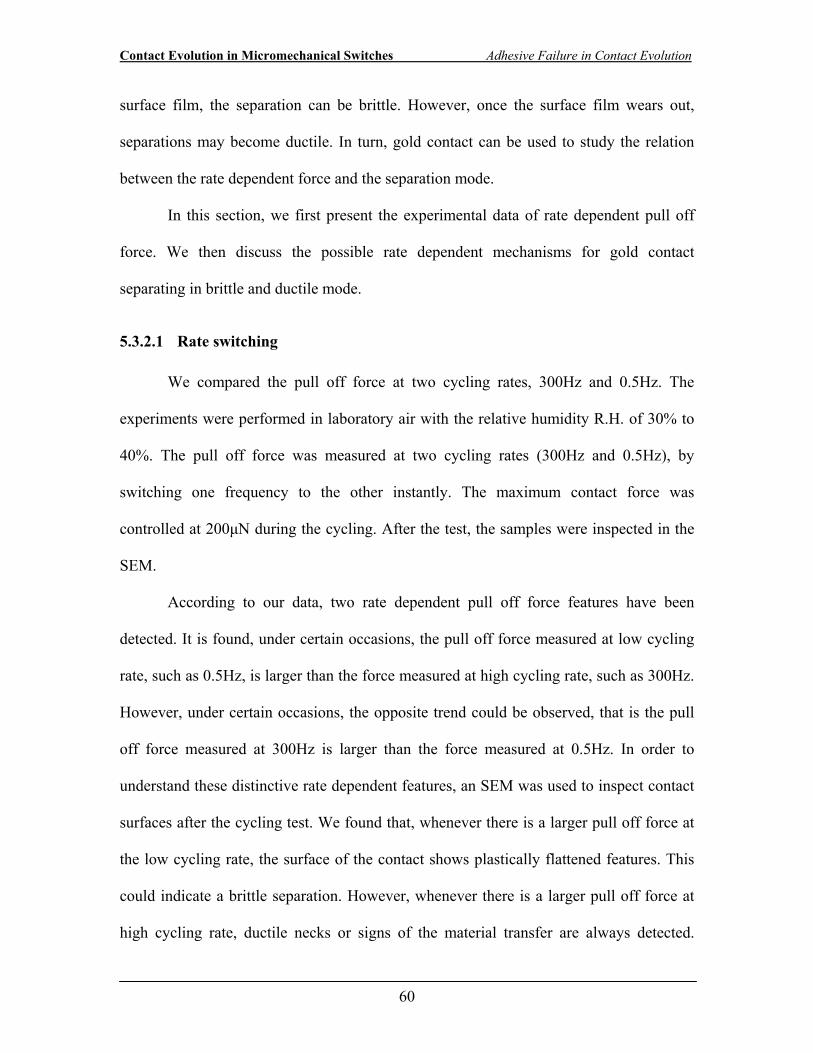
Contact Evolution in Micromechanical Switches Adhesive Failure in Contact Evolution
60
surface film, the separation can be brittle. However, once the surface film wears out,
separations may become ductile. In turn, gold contact can be used to study the relation
between the rate dependent force and the separation mode.
In this section, we first present the experimental data of rate dependent pull off
force. We then discuss the possible rate dependent mechanisms for gold contact
separating in brittle and ductile mode.
5.3.2.1 Rate switching
We compared the pull off force at two cycling rates, 300Hz and 0.5Hz. The
experiments were performed in laboratory air with the relative humidity R.H. of 30% to
40%. The pull off force was measured at two cycling rates (300Hz and 0.5Hz), by
switching one frequency to the other instantly. The maximum contact force was
controlled at 200μN during the cycling. After the test, the samples were inspected in the
SEM.
According to our data, two rate dependent pull off force features have been
detected. It is found, under certain occasions, the pull off force measured at low cycling
rate, such as 0.5Hz, is larger than the force measured at high cycling rate, such as 300Hz.
However, under certain occasions, the opposite trend could be observed, that is the pull
off force measured at 300Hz is larger than the force measured at 0.5Hz. In order to
understand these distinctive rate dependent features, an SEM was used to inspect contact
surfaces after the cycling test. We found that, whenever there is a larger pull off force at
the low cycling rate, the surface of the contact shows plastically flattened features. This
could indicate a brittle separation. However, whenever there is a larger pull off force at
high cycling rate, ductile necks or signs of the material transfer are always detected.
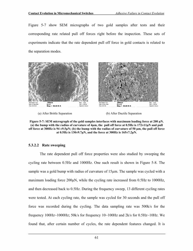
Contact Evolution in Micromechanical Switches Adhesive Failure in Contact Evolution
61
Figure 5-7 show SEM micrographs of two gold samples after tests and their
corresponding rate related pull off forces right before the inspection. These sets of
experiments indicate that the rate dependent pull off force in gold contacts is related to
the separation modes.
(a) After Brittle Separation (b) After Ductile Separation
Figure 5-7: SEM micrograph of the gold samples interfaces with maximum loading force at 200 μN. (a) the bump with the radius of curvature of 4µm, the pull off force at 0.5Hz is 172±11μN and pull
off force at 300Hz is 94 ±9.5μN; (b) the bump with the radius of curvature of 50 µm, the pull off force at 0.5Hz is 130±9.7μN, and the force at 300Hz is 165±7.2μN.
5.3.2.2 Rate sweeping
The rate dependent pull off force properties were also studied by sweeping the
cycling rate between 0.5Hz and 1000Hz. One such result is shown in Figure 5-8. The
sample was a gold bump with radius of curvature of 15µm. The sample was cycled with a
maximum loading force 200μN, while the cycling rate increased from 0.5Hz to 1000Hz,
and then decreased back to 0.5Hz. During the frequency sweep, 13 different cycling rates
were tested. At each cycling rate, the sample was cycled for 30 seconds and the pull off
force was recorded during the cycling. The data sampling rate was 500k/s for the
frequency 100Hz~1000Hz; 50k/s for frequency 10~100Hz and 2k/s for 0.5Hz~10Hz. We
found that, after certain number of cycles, the rate dependent features changed. It is
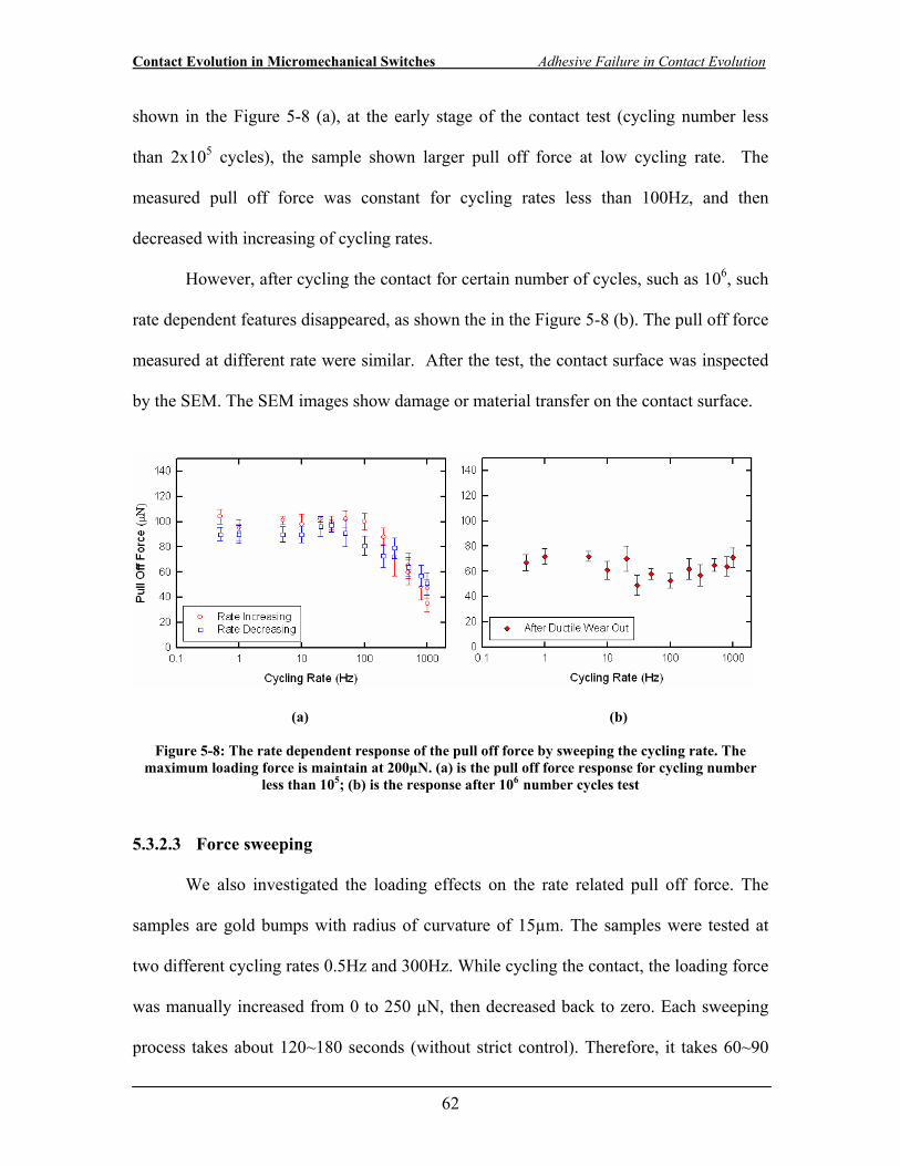
Contact Evolution in Micromechanical Switches Adhesive Failure in Contact Evolution
62
shown in the Figure 5-8 (a), at the early stage of the contact test (cycling number less
than 2x10⁵ cycles), the sample shown larger pull off force at low cycling rate. The
measured pull off force was constant for cycling rates less than 100Hz, and then
decreased with increasing of cycling rates.
However, after cycling the contact for certain number of cycles, such as 106, such
rate dependent features disappeared, as shown the in the Figure 5-8 (b). The pull off force
measured at different rate were similar. After the test, the contact surface was inspected
by the SEM. The SEM images show damage or material transfer on the contact surface.
(a) (b)
Figure 5-8: The rate dependent response of the pull off force by sweeping the cycling rate. The maximum loading force is maintain at 200µN. (a) is the pull off force response for cycling number
less than 105; (b) is the response after 106 number cycles test 5.3.2.3 Force sweeping
We also investigated the loading effects on the rate related pull off force. The
samples are gold bumps with radius of curvature of 15µm. The samples were tested at
two different cycling rates 0.5Hz and 300Hz. While cycling the contact, the loading force
was manually increased from 0 to 250 µN, then decreased back to zero. Each sweeping
process takes about 120~180 seconds (without strict control). Therefore, it takes 60~90
Contact Evolution in Micromechanical Switches Adhesive Failure in Contact Evolution
63
contact cycles to finish the force sweeping at 0.5Hz and 3x10⁴ ~ 5x10⁴ contact cycles for
the force sweeping at 300Hz. The force sweeping was first performed at 0.5Hz, and then
followed by the 300Hz test. The pull off force was recorded correspondingly. According
to the surface condition, the separation for the gold contacts can either be brittle or
ductile. Figure 5-9 shows the two typical characteristics for rate related pull off force.
(a) (b)
Figure 5-9: Rate dependent pull off force for separation with (a) larger force at low rate, and (b) larger force at high rate.
Figure 5-9 (a) shows pull off force data sampled at an early stage of the contact
evolution. The total cycle number after the sweeping test was less than 5x10⁴ cycles. It is
shown that the pull off force measured at 0.5Hz is larger than the pull off force measured
at 300Hz. The difference increases with the increasing of the loading. It is also noted that
the pull off force as the loading is decreased is slightly higher than the force as the
loading is increased. This is probably due to the wear out of the surface film during the
test.
Contact Evolution in Micromechanical Switches Adhesive Failure in Contact Evolution
64
The other feature is usually observed after cycling the contact for more than 105
cycles. As shown in Figure 5-9(b), for loading forces less than 200μN, the pull off force
at low cycling rates is almost the same as the force measured at high cycling rate.
Furthermore, for loading forces larger than 200μN, the pull off force measured at 300Hz
is larger than the force measured at 0.5Hz. For a loading force of 250µN, there is 40µN
difference in the pull off force between two cycling rate. For contact surfaces with larger
force at high rate, the damage or material transfer have been observed in the SEM.
5.3.2.4 Data interpretation
According to our rate-dependent pull off contact tests, there are two different rate-
dependent features have been identified. One feature shows a larger pull off force at low
cycling rates. The other feature shows a larger pull off force at high cycling rates.
Correspondingly, the SEM images show that the contacts with larger pull off force at low
cycling rate have plastically flattened surfaces. However, surface damage has been
observed on contacts with larger pull off forces at high cycling rates. These observations
suggest that the rate dependent pull off force features depend on the separation modes.
The larger pull off force at low cycling rates indicates a brittle separation. On the other
hand, the larger pull off force at high cycling rates may indicate a ductile separation.
These results are similar to the rate dependent pull off force studies in polymer and
frictional force. However, to our best knowledge, it is the first time that the rate
dependent pull off force have been used to study the separation modes in metal contacts.
In following discussion, I will identify the separation modes by the measured rate
Contact Evolution in Micromechanical Switches Adhesive Failure in Contact Evolution
65
dependent pull off force, and discuss two separation modes in our rate sweeping and load
sweeping tests.
In brittle mode, the bonding strength at the interfaces determines the magnitude of
the pull off force. The longer time in contact, the stronger bonding could develop, which
in turn need larger pull off force to separate the contacts. There is longer time in contact
at low cycling rate than it is at higher cycling rate. Thus, we would expect larger pull off
force at low cycling rate. For gold contacts, such brittle features are usually detected in
the early phase of the cycling test, i.e. with the cycling number less than 105. One
possible explanation is that at the early stage of the cycling test, the contact surface is
usually coated with a layer of the surface film. This layer of the surface film could lower
the surface energy and keep the separation in brittle mode.
Figure 5-8 (a) shows a rate sweeping test in brittle mode. It is noted there is a
transition frequency (100Hz) in the rate sweeping test. For cycling rate less than 100Hz,
the magnitude of the pull off forces measured at different rate are almost the same.
However, for cycling rate larger than 100Hz, the increasing of the rate will lead to the
decrease of the pull off force. Considering the magnitude of the pull off force in the
brittle mode is related to the bonding strength between the interfaces, it seems that there
is a time constant for developing the interfacial bonding. For the contact time shorter than
this time constant, there are fewer bonds would develop; in turn less pull off force is
needed. However, for the contact time longer than this time constant, the bonding
development reaches an equilibrium status. Further increasing of the contact time will not
significantly increase the pull off force. In this test, with a transition frequency of 100Hz,
Contact Evolution in Micromechanical Switches Adhesive Failure in Contact Evolution
66
the time constant is about 5ms. This rate dependent feature will be further discussed in
next section.
Figure 5-9 (a) shows the loading sweeping test in brittle mode. With the increase
of loading, the differences between the pull off force at two cycling rate increases. The
increase of the pull off force could be due to that the larger loading can lead to stronger
bonding. To evaluate the bonding strength, we estimate the work of adhesion. Assume
that during the brittle separation, the magnitude of the pull off force equal to the contact
adhesion, which can be estimated by JKR model, and RwFpulloff ⋅⋅⋅= π5.1 . Here, R is the
radius of the curvature of contact bump, and w is the work of the adhesion. Based upon
JKR, for contact bump with radius of curvature of 15µm, 40µN measured pull off force
corresponds to the work of adhesion of 0.56J/m2; 80 µN measured pull off force
corresponds to the work of adhesion 1.13J/m2.
However, after contact test, we observed plastic deformation region on top of the
contact bump. Assuming all the plastic deformation occurs during the first cycle of
loading, the unloading and the next cycle of loading are elastic. Due to plastic
deformation the effective asperity radius of curvature Reff after elasto-plastic or fully
plastic deformation is different than its initial value R. Correspondingly, the pull off force
should be expressed in term of Reff, effpulloff RwF ⋅⋅⋅= π5.1 . In order to estimate the
effective radius of curvature, we first estimate the hardness of gold thin film. The film
hardness determined the area of plastic deformation. For nominal flattened area with
radius of Ra, the hardness H can be roughly estimated by )/( 2aRFH ⋅= π , F is the
loading force. In our test, the radius of the flattened area is in the range of 350nm to
500nm, which gives estimated hardness values ranging from 250MPa to 500MPa.
Contact Evolution in Micromechanical Switches Adhesive Failure in Contact Evolution
67
Consider that the size of the nominal flattened area could also be affected by sliding or
contact creep effects. We choose 350nm contact radius as a reference for hardness
estimation, which gives a hardness value of 500MPa. Notice that this value is much less
than the hardness value measured by nanoindenter (Table 6-1). The different hardness
value could be due to different material responses at two length scale. In this contact test,
the plastic response is at micro-scale. However, the hardness measurement using the
nanoindenter is at nano-scale. The lower hardness at micro-scale could be due to defects
and/or grain boundaries serving as dislocation sources which may not be available at the
nano-scale test.
The effective radius of curvature after a single loading event can be estimated by
Kogut-Etsion (KE)’s curve fitting solutions from finite element analysis [50,51]. Using KE
model, for the bump, with original radius of curvature R=15µm, hardness H=500MPa,
and loading force F=200µN, the effective radius of the curvature Reff is calculated as
45µm. Based on JKR mode, with the effective radius of curvature mReff μ45= , the work
of adhesion can be calculated as 0.37J/m2 for 80 µN pull off force; the work of adhesion
is 0.18J/m2 for 40µN pull off force. These values of work of adhesion are much smaller
than the work of adhesion between clean metal contacts (1~3J/m2), which indicates that
there are surface films between the gold contacts. These interposed films can keep the
separation in brittle mode.
In ductile mode, the bulk properties, such as viscosity and plasticity, determine
the magnitude of the pull off force. The larger pull off force at high cycling rates suggests
there are viscous effects during the separation. We will discuss the viscous effects in
section 5.3.4. Generally, for gold contacts, ductile separation is usually observed after
Contact Evolution in Micromechanical Switches Adhesive Failure in Contact Evolution
68
certain number of cycling (such as cycle number larger than 105). This observation may
indicate that wear-out of the surface film causes the separation rate mode to change from
brittle to ductile. It is shown that, in the ductile mode, the magnitude of the pull off force
could be 30 ~40µN different at two cycling rates. And the difference increases with
increased loading. Considering that the magnitude of the pull off force in the ductile
mode is related to the ductile area, the increase in the pull off force may indicate the
increase of the ductile area.
Note that the magnitude of the pull off force in the ductile mode is not necessary
larger than the force in the brittle mode. This feature may be due to that ductile separation
happens over small areas, such as the nano scale, and the small areas of ductile fracture
do not necessary increase the overall pull off force. Furthermore, pulling out of nanoscale
ductile necks could cause the mixture of gold atoms and contaminants in the air, which
could change the gold thin film properties. In turn, there may not be pure metal-to-metal
contact after several ductile separations. Let us simply estimate the work of adhesion
from the measured pull off force using JKR model. In Figure 5-9 (b), at the loading of
200µN, the pull off force measured at 0.5Hz is 60 µN. With the original radius of
curvature of 15µm, the work of adhesion is 0.85J/m2. However, with effective radius of
curvature 45 µm, the work of adhesion is 0.28J/m2.
5.3.3 Rate Effects in Brittle Mode
In this section, a possible mechanism for the rate effects in the brittle mode is
proposed. Since the magnitude of the pull off force in brittle mode is related to the
surface conditions. Therefore, it is expected that the rate dependent pull off force in the
Contact Evolution in Micromechanical Switches Adhesive Failure in Contact Evolution
69
brittle mode can be related to the dynamic response at the surfaces. Considering gold
contacts in particular, the gold surface is usually coated with a thin layer of the water
when it is exposed to the ambient air [52]. It is less than one molecular layer thick.
However, due to the presence of this water film, menisci can form between the small
gaps when two surfaces come together. These menisci can increase the pull off force by
introducing the meniscus force into the contact adhesion. The condensation of water
menisci has been known to cause stiction problems in magnetic disks [53]. Since the
generation and growth of capillary condensation is time dependent process, the kinetic of
the capillary condensation could be one factor in the rate related pull off force in the
brittle mode.
In general, the resting time in contact determines the number of the forming
meniscus bridges. The experiments by Szoszkiewicz [54] have shown that at 37% relative
humidity, the mean meniscus nucleation time is around 0.7~4.2ms at room temperature.
For contact times less than the mean nucleation time, the number of menisci forming will
be reduced. The longer the time in contact, the more menisci can be developed, hence the
larger meniscus force. Our rate sweeping experiment shows that the pull off force drops
when the cycling rate is larger than 100Hz. This may indicate the equilibrium time for
meniscus condensation is about 5ms, which is in the range of the meniscus nucleation
time scales observed by Szoszkiewicz. Further increasing the cycling rate could cause
some meniscus bridges to fail to nucleate.
Based on these analyses, the larger pull off force measured at low cycling rate
could be due to the meniscus force effect. According our data, the force differences
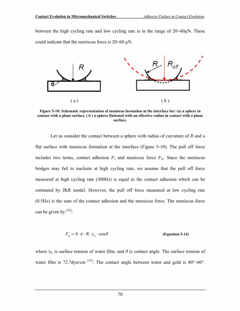
Contact Evolution in Micromechanical Switches Adhesive Failure in Contact Evolution
70
between the high cycling rate and low cycling rate is in the range of 20~60µN. These
could indicate that the meniscus force is 20~60 µN.
( a ) ( b )
Figure 5-10: Schematic representation of meniscus formation at the interface for: (a) a sphere in contact with a plane surface, ( b ) a sphere flattened with an effective radius in contact with a plane
surface.
Let us consider the contact between a sphere with radius of curvature of R and a
flat surface with meniscus formation at the interface (Figure 5-10). The pull off force
includes two terms, contact adhesion Fs and meniscus force Fm. Since the meniscus
bridges may fail to nucleate at high cycling rate, we assume that the pull off force
measured at high cycling rate (300Hz) is equal to the contact adhesion which can be
estimated by JKR model. However, the pull off force measured at low cycling rate
(0.5Hz) is the sum of the contact adhesion and the meniscus force. The meniscus force
can be given by [53]:
θγπ cos4 ⋅⋅⋅⋅= lvm RF (Equation 5-14)
where γlv is surface tension of water film, and θ is contact angle. The surface tension of
water film is 72.7dyn/cm [55]. The contact angle between water and gold is 40°~60°.
Contact Evolution in Micromechanical Switches Adhesive Failure in Contact Evolution
71
However, since there is a layer of water thin film on gold surface, the contact angle can
be chosen as zero. Here, we use θ =0° to estimate the magnitude of the meniscus force.
According to Equation 5-14, for a meniscus force in the range of 20~60µN, the
contact radius of curvature need to be 25~70µm. Notice that the original radius of
curvature of our contact bumps are 4~50 µm. After contact test, the top of the bump
surface have been plastically flattened, which could increase the effective radius of
curvature, also increase the meniscus effects. Take an example from section 5.3.2.3. At
the loading force of 200µN, the pull off force measured at 0.5Hz is 80µN and the force
measured at 300Hz is 40µN. This may indicate the meniscus force is 40µN. Using
Equation 5-14, the equivalent radius of curvature is calculated as 45µm. Notice that is the
effective contact radius value estimated by KE model. This analysis shows that the
flattened contact surface lead to large meniscus force.
However, after ductile separation, the contact surface have been damaged, the
surface roughness can be significantly increase. Under these conditions, the menisci can
only condense around the several tall asperities. Assume the contact has N=10 tall
asperities with radius of the curvature Rp is 500nm. The meniscus force can be estimated
as:
NRF lvpm ⋅⋅⋅⋅⋅= θγπ cos4 (Equation 5-15)
The calculation gives meniscus force of about 4.3 µN (γlv=72.7dyn/cm, θ=0°). This may
explain that the measured force value in Figure 5-8 (b). After the ductile damage, the
measured forces were similar at different cycling rates.
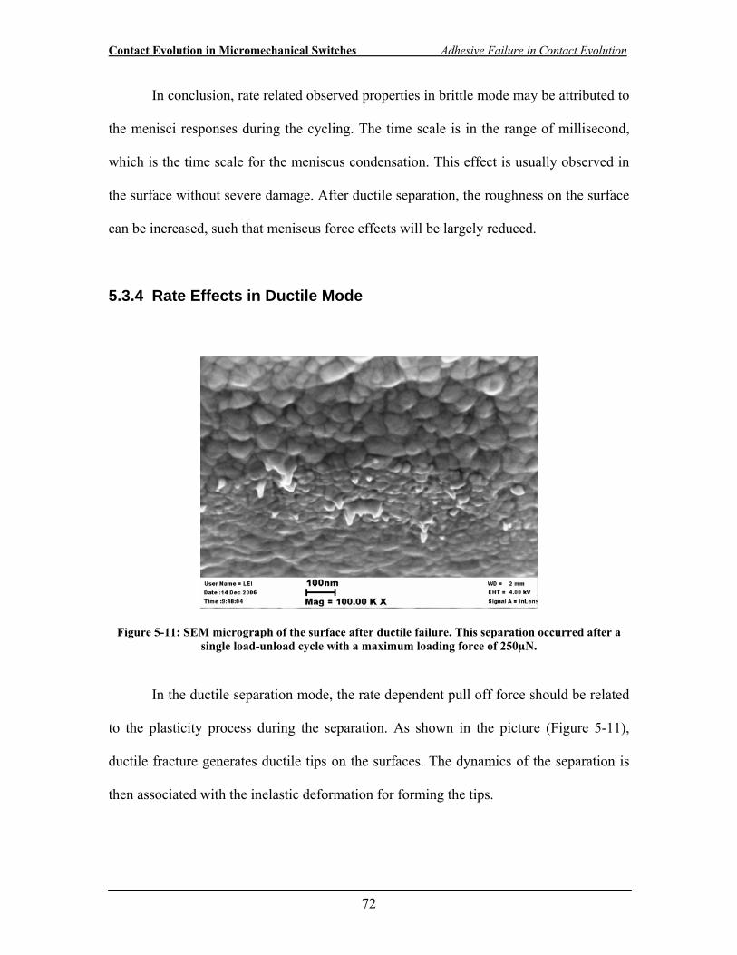
Contact Evolution in Micromechanical Switches Adhesive Failure in Contact Evolution
72
In conclusion, rate related observed properties in brittle mode may be attributed to
the menisci responses during the cycling. The time scale is in the range of millisecond,
which is the time scale for the meniscus condensation. This effect is usually observed in
the surface without severe damage. After ductile separation, the roughness on the surface
can be increased, such that meniscus force effects will be largely reduced.
5.3.4 Rate Effects in Ductile Mode
Figure 5-11: SEM micrograph of the surface after ductile failure. This separation occurred after a single load-unload cycle with a maximum loading force of 250µN.
In the ductile separation mode, the rate dependent pull off force should be related
to the plasticity process during the separation. As shown in the picture (Figure 5-11),
ductile fracture generates ductile tips on the surfaces. The dynamics of the separation is
then associated with the inelastic deformation for forming the tips.
Contact Evolution in Micromechanical Switches Adhesive Failure in Contact Evolution
73
For metals, inelastic deformation can be either time-independent “yield” flow, or
the time-dependent “creep” flow [56]. The “yield” flow defines the perfectly plastic
behavior observed in metals. At room temperature, the yield flow is the dominant
deformation mechanism in a macroscopic crystalline metal. The physical mechanism for
yield flow can be described as the nucleation and propagation of crystallographic defects,
or dislocations. The dislocations can move fast once they are activated. Thus, the time
scale for yield flow is usually neglected in the normal experimental conditions.
The time dependent “creep” flow determines the viscous effects during the
inelastic deformation. In a metal, the time dependent deformation mechanisms can be
dislocation glide, dislocation climb, and/or diffusion flow. These mechanisms contribute
to the “creep” behavior in metals. The time dependent mechanisms are usually associated
with the existence of a thermal activation barrier for diffusion or the short barrier for
dislocation nucleation. Since creep flow generally occurs in response to a stress-aided
thermal activation, the time dependent responses are usually observed in higher
temperature.
In this study, we observed the time related response during ductile separation.
This indicates the time-dependent deformation mechanisms are activated or may be
dominant during contact opening. This behavior is rarely observed in metals at macro
scale and room temperature. As shown in the SEM micrograph (Figure 5-11), the ductile
separation has caused nano scale tips to be pulled out on the surface. The length scale of
these structures could be the reason for the viscous effects. I will first review the study of
plastic deformation at the nano scale and its underlying mechanisms. Following that, a
viscous liquid model is used to explain the viscous response during ductile separation.
Contact Evolution in Micromechanical Switches Adhesive Failure in Contact Evolution
74
5.3.4.1 Plasticity at the nano scale
Physical properties of the structure at nanometer scales can be significantly
different from those at the macro scale. One significant feature is that the hardness at the
nanometer scale structures increases due to a lack of dislocation sources. At the same
time, by increasing the surface-to-volume ratio, the internal cohesive bonding strength
can be affected by the surface tension of the nanostructures. For instance [57], it is found
that nanometer scale clusters and ultrathin metallic nanowires have much lower melting
temperatures than their bulk counterparts. The melting point for a 4.6nm Pd nanowire
was observed as 300°C, while the bulk melting point of Pd is 1445°C [58] . Surface
tension driven diffusion has also been observed to cause mass transport in small
asperities [59]. All these features could cause “creep” flow to be the dominant mechanism
in nanometer scale plasticity.
Ductile separation at a nano junction has been studied by Molecular Dynamic
(MD) simulations [60,61] and/or experimentally using STM [62] or HRSTM [63]. Those
studies show that, lacking the dislocation mechanism, the nano junction is elongating by
the slips of atom planes and the rearrangement of the atoms forming new atom layers.
There are two possible slip mechanisms. For relative large tips (>20nm), the slip occurs
by gliding of the dislocation which is nucleated at the surface. For the smaller nano
junction (<10nm), the slip is largely observed as the homogeneous shearing of the atom
plane. When different slip planes are activated, the intersection of the slips will generate
disorders. The disorder will pin down the movement of the dislocation. However, it is
observed that the atoms around the disorder can rearrange themselves. The atom
rearrangement can anneal out the disorder and form a new atomic layer. A new slip plane
Contact Evolution in Micromechanical Switches Adhesive Failure in Contact Evolution
75
will then be activated afterward. This slip-disorder-slip mechanism is time related
response, and it has shown strong strain rate dependence. MD simulations have
demonstrated that at higher temperatures and lower strain rate, a higher degree of
crystalline structure is favored due to the atom arrangement. As the tips (or necks)
elongate, the structure will turn to a few totally disordered atom chains before rupturing.
One thing that should be mentioned here is that due to the computer time, the MD
simulation is generally performed at a higher strain rate than normal experimental
conditions. The strain rate for MD simulations is typically larger than 108s-1. Under this
condition, the diffusion effect is ignored.
On the experimental side, surface tension driven diffusion has been observed in
the separation of Au/Au [63] and Pb/Au [62] nano junctions. Surface diffusion allows mass
transport during elongation of the junction. The mobile atoms can either enhance the
growth of the neck or the thinning of the neck depending on the curvature. The diffusion
driven material flow has also observed in Au/Au thin film [64] separation. Fast moving
atoms on the surface are due to lower barrier height for atom diffusion around the
nanostructure. Even though it is unrealistic to assume the nano junction is a liquid, it is
believed that at the last stage of the separation, (when the neck is narrowing down to
several nanometer), the junction behaves like a “liquid” [60].
According to the studies of ductile separation at the nano junction, two time-
related inelastic mechanisms have been activated during the ductile elongation. One is the
atom rearrangement, i.e. the disorder atoms prefer to be reordered following the
crystalline structure. The other one is the diffusion flow. Both mechanisms will cause
time-dependent relaxation during the separation. Note that both relaxation mechanisms
Contact Evolution in Micromechanical Switches Adhesive Failure in Contact Evolution
76
are related to the self-diffusivity. We can evaluate viscous effects in the ductile tips by
assuming them as viscous liquid bridges. The viscosity of these liquid bridges is
determined by the diffusivity of the nanostructures. According to the Boltzmann-
Arrhenius dependency law, the diffusion coefficient can be expressed as:
)exp(0 kTEDD a−⋅= (Equation 5-16)
where 0D is the pre-exponential diffusion coefficient, Ea is the activation energy for the
diffusion, k is Boltzmann constant, and T is the temperature (K). For bulk gold, the
120 sec3.0 −⋅= cmD [65], and
)()1089.4( 4 eVTE ma ⋅×= − (Equation 5-17)
mT is the melting temperature of materials. The melting temperature for nano scale
structure has been observed much less then the bulk crystal. Using liquid-drop model [66],
the melting temperature Tm for a nano cylindrical geometry can be expressed as:
⎟⎠⎞
⎜⎝⎛ +−=
ldTT
mb
m 246
1 β (Equation 5-18)
where d (nm) is the diameter and l (nm) is the length for the nanostructure. Tmb is the
melting temperature for bulk material and β is a material constant (β=1.1281nm for gold).
For a gold cylindrical nanostructure, with assumed dimension of d=30nm, l=40nm, the
Contact Evolution in Micromechanical Switches Adhesive Failure in Contact Evolution
77
melting temperature for nanostructure is 1291K, with bulk melting temperature
Tmb=1337K. Smaller values of d and/or l lead to a greater difference in melting
temperature from the bulk value. Therefore, at room temperature, for Tm=1291K, the
activation energy for atom diffusion is Ea=0.63eV (using Equation 5-17). The diffusion
coefficient is then given as D=0.32x10⁻¹⁵m2.sec-1. This value is in the range with the
experimental value (10-15 m2.sec-1) from Alcantar et al. [64]. They estimated the diffusion
coefficient of gold contact by observing the ductile separation between gold thin films.
Further it is assumed that the gold atoms are following the law of Brownian
motion. The viscosity of this liquid medium η can be expressed by Stokes-Einstein
formula [67]
DkT
⋅Ω⋅⋅= 3/16 π
η (Equation 5-19)
where, Ω is atomic volume and 3291066.1 m⋅⋅=Ω − for Au. The viscosity coefficient of
the gold nanotips, with diameter of 30nm and length of 40nm, can be calculated
as 1sec2596 −⋅= Paη . With this viscosity coefficient, we proposed to model the ductile
elongating tip as a capillary liquid bridge building between two surfaces. The detail
analysis is shown as following.
5.3.4.2 Viscous force
Assume the liquid is a cylinder structure, with the radius of a0 and the height of
D0. In order to simplify the problem, we also assume that this nano structure behaves like
a Newtonian fluid. When two surfaces are moving apart with a confined liquid bridge in
Contact Evolution in Micromechanical Switches Adhesive Failure in Contact Evolution
78
between, the pull off force has to overcome the attractive force Fad from the liquid bridge.
There are two terms in the attractive force[68], one is the meniscus force Fm due to the
surface tension, and the other is the viscous force Fv due to the viscosity of the liquid.
vmad FFF += (Equation 5-20)
The meniscus force Fm is related to the liquid volume and the contact angle, and it is
independent of the velocity. The meniscus force for confined liquid between two flat
surfaces can be expressed as [69]:
hAFm
)cos(cos 21 θθγ +⋅⋅= (Equation 5-21)
where A is the total area for the confined liquid, h is the height of the liquid and the θ1
and θ2 are the contact angle between the liquid and upper and lower two surfaces. Since
in our case, all the materials are gold, we choose zero for both angles. Thus the capillary
force for the nano tip with the surface tension of γ can be expresses as [70]:
0
202
DaFm
γπ ⋅⋅⋅= (Equation 5-22)
The viscous force due to viscous liquid is related to the separation interval time ∆t and
the liquid viscosity η [71]:
Contact Evolution in Micromechanical Switches Adhesive Failure in Contact Evolution
79
tFv Δ⋅= /ηβ (Equation 5-23)
where, β is a proportionality constant, which is related to the dimension of the structure.
In order to estimate the magnitude of viscous force for nanotips, we follow Matthewson’s
impulse approach. A viscous impulse Iv is introduced, which is defined as the time
integral of viscous force [72], i.e.:
∫Δ
⋅=t
vv dtFI0
(Equation 5-24)
In our test, during the separation interval, the increment of the attractive force from liquid
bridge is balanced by the spring force Fs exerted by the cantilever with a stiffness of k. If
we assume the meniscus force is constant during this short period, then the change of the
viscous force can be given as:
kVdt
dFdt
dFdt
dF svad === (Equation 5-25)
where V is the separation velocity, which is controlled by the displacement of
piezoelectric actuator. Driven by the movement of the piezoelectric actuator, the viscous
force increases linearly like a ramp force, and the maximum viscous force right before
the breaking point Fvm is:
tVktFFvm Δ⋅⋅=Δ⋅=•
(Equation 5-26)
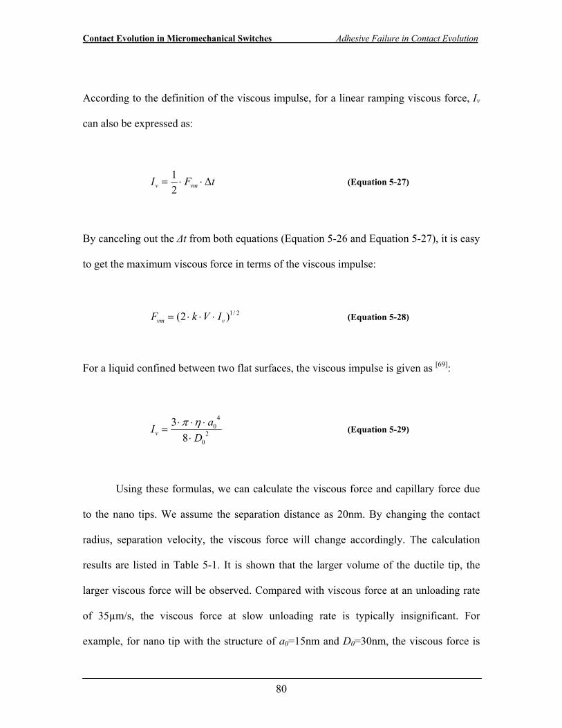
Contact Evolution in Micromechanical Switches Adhesive Failure in Contact Evolution
80
According to the definition of the viscous impulse, for a linear ramping viscous force, Iv
can also be expressed as:
tFI vmv Δ⋅⋅=21
(Equation 5-27)
By canceling out the Δt from both equations (Equation 5-26 and Equation 5-27), it is easy
to get the maximum viscous force in terms of the viscous impulse:
2/1)2( vvm IVkF ⋅⋅⋅= (Equation 5-28)
For a liquid confined between two flat surfaces, the viscous impulse is given as [69]:
20
40
83
DaIv ⋅⋅⋅⋅
=ηπ
(Equation 5-29)
Using these formulas, we can calculate the viscous force and capillary force due
to the nano tips. We assume the separation distance as 20nm. By changing the contact
radius, separation velocity, the viscous force will change accordingly. The calculation
results are listed in Table 5-1. It is shown that the larger volume of the ductile tip, the
larger viscous force will be observed. Compared with viscous force at an unloading rate
of 35µm/s, the viscous force at slow unloading rate is typically insignificant. For
example, for nano tip with the structure of a0=15nm and D0=30nm, the viscous force is
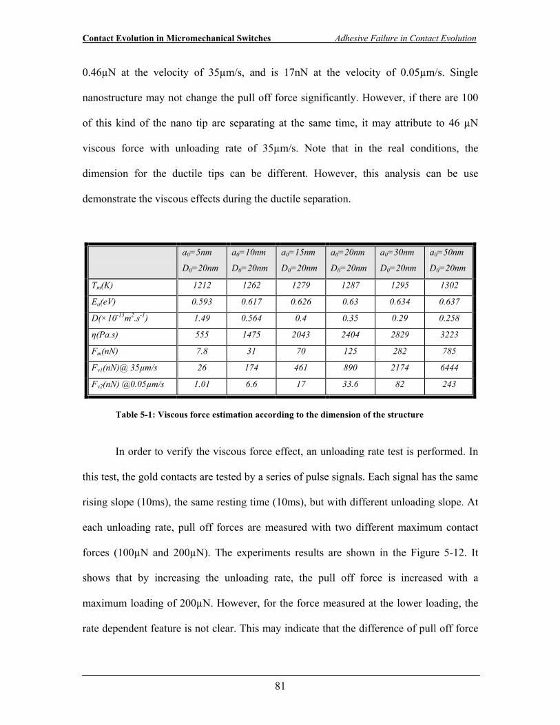
Contact Evolution in Micromechanical Switches Adhesive Failure in Contact Evolution
81
0.46µN at the velocity of 35µm/s, and is 17nN at the velocity of 0.05µm/s. Single
nanostructure may not change the pull off force significantly. However, if there are 100
of this kind of the nano tip are separating at the same time, it may attribute to 46 µN
viscous force with unloading rate of 35µm/s. Note that in the real conditions, the
dimension for the ductile tips can be different. However, this analysis can be use
demonstrate the viscous effects during the ductile separation.
a0=5nm
D0=20nm
a0=10nm
D0=20nm
a0=15nm
D0=20nm
a0=20nm
D0=20nm
a0=30nm
D0=20nm
a0=50nm
D0=20nm
Tm(K) 1212 1262 1279 1287 1295 1302
Ea(eV) 0.593 0.617 0.626 0.63 0.634 0.637
D(×10-15m2.s-1) 1.49 0.564 0.4 0.35 0.29 0.258
η(Pa.s) 555 1475 2043 2404 2829 3223
Fm(nN) 7.8 31 70 125 282 785
Fv1(nN)@ 35µm/s 26 174 461 890 2174 6444
Fv2(nN) @0.05µm/s 1.01 6.6 17 33.6 82 243
Table 5-1: Viscous force estimation according to the dimension of the structure
In order to verify the viscous force effect, an unloading rate test is performed. In
this test, the gold contacts are tested by a series of pulse signals. Each signal has the same
rising slope (10ms), the same resting time (10ms), but with different unloading slope. At
each unloading rate, pull off forces are measured with two different maximum contact
forces (100µN and 200µN). The experiments results are shown in the Figure 5-12. It
shows that by increasing the unloading rate, the pull off force is increased with a
maximum loading of 200µN. However, for the force measured at the lower loading, the
rate dependent feature is not clear. This may indicate that the difference of pull off force
Contact Evolution in Micromechanical Switches Adhesive Failure in Contact Evolution
82
in the ductile may related to the ductile volume. By increasing the loading force, the
ductile volume is also increasing.
(a) (b)
Figure 5-12: Pull off force test with different unloading velocity. (a) The driving waveform for the test. Each pulse with the same loading slope and the same time in contact, however, the unloading
slop is different; (b) measured unloading rate dependent pull off force in the ductile mode.
Both the model and unloading rate tests indicate the viscous effects during the
ductile separation. It is observed in our cycling testing, when there is significant ductile
separation, the force measured at 300Hz cycling rate is usually 30 ~50µN higher than the
force measured at 0.05Hz. 300Hz cycling is corresponding to the unloading rate of
35µm/s. And 0.05Hz cycling is corresponding to the unloading rate of 0.05µm/s. These
rate dependant features may due to the generation of the ductile tips and their
corresponding viscous effects.
In conclusion, ductile separation will generate the nano tips on the surface. During
the elongation of those nano structures, time-dependent deformation mechanisms are
activated. In nano scale junctions, surface tension driven diffusion, and atom
reorganization during ductile separation contribute to this time related plasticity. A
viscous liquid model is used to conceptually explain the observed responses. Due to this
Contact Evolution in Micromechanical Switches Adhesive Failure in Contact Evolution
83
viscous effect, the pull off force increase with increase of the cycling rate when the
separation is under the ductile mode.
5.4 Contact Evolution and Separation Modes
The evolution of contact is studied by cycling the contacts and monitoring the
characteristics of the pull off force. The force characteristics, such as the magnitude of
the pull-off force, the force vs. displacement curves, and the rate-dependent pull-off force
are sampled during cycling. The force vs. displacement curves and rate-dependent pull
off force are used to identify the separation modes. By monitoring the change of the pull
off force and its corresponding separation mode, we found that the evolution patterns of
the force (or contact) are strongly affected by the separation modes.
5.4.1 Force Evolution in Au/Au Contacts
In this section, Au/Au contacts are used to demonstrate the relationship between the
separation modes and contact evolution. Preliminary Au/Au contact tests have been
performed by using a hemispherical bump and planar substrate. The hemispherical
contact bump was micro-fabricated on top of the cantilever, with a base diameter of 4μm
and a height from the base of 0.5μm. The radius of curvature of the contact bump is
15μm. Both the cantilever and the planar substrate were coated with 200nm of sputtered
gold. The tests were performed in room air at room temperature. The contact force was
controlled at 250μN during the cyclic test and the pull off force was recorded
correspondingly. Since the planar substrate and the cantilever were set parallel to each
other, there may be 1~2nm sliding along the surface during the cyclic test (Section 4.5).
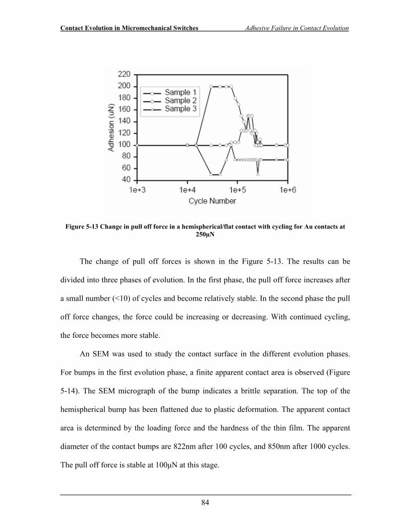
Contact Evolution in Micromechanical Switches Adhesive Failure in Contact Evolution
84
Figure 5-13 Change in pull off force in a hemispherical/flat contact with cycling for Au contacts at 250µN
The change of pull off forces is shown in the Figure 5-13. The results can be
divided into three phases of evolution. In the first phase, the pull off force increases after
a small number (<10) of cycles and become relatively stable. In the second phase the pull
off force changes, the force could be increasing or decreasing. With continued cycling,
the force becomes more stable.
An SEM was used to study the contact surface in the different evolution phases.
For bumps in the first evolution phase, a finite apparent contact area is observed (Figure
5-14). The SEM micrograph of the bump indicates a brittle separation. The top of the
hemispherical bump has been flattened due to plastic deformation. The apparent contact
area is determined by the loading force and the hardness of the thin film. The apparent
diameter of the contact bumps are 822nm after 100 cycles, and 850nm after 1000 cycles.
The pull off force is stable at 100μN at this stage.
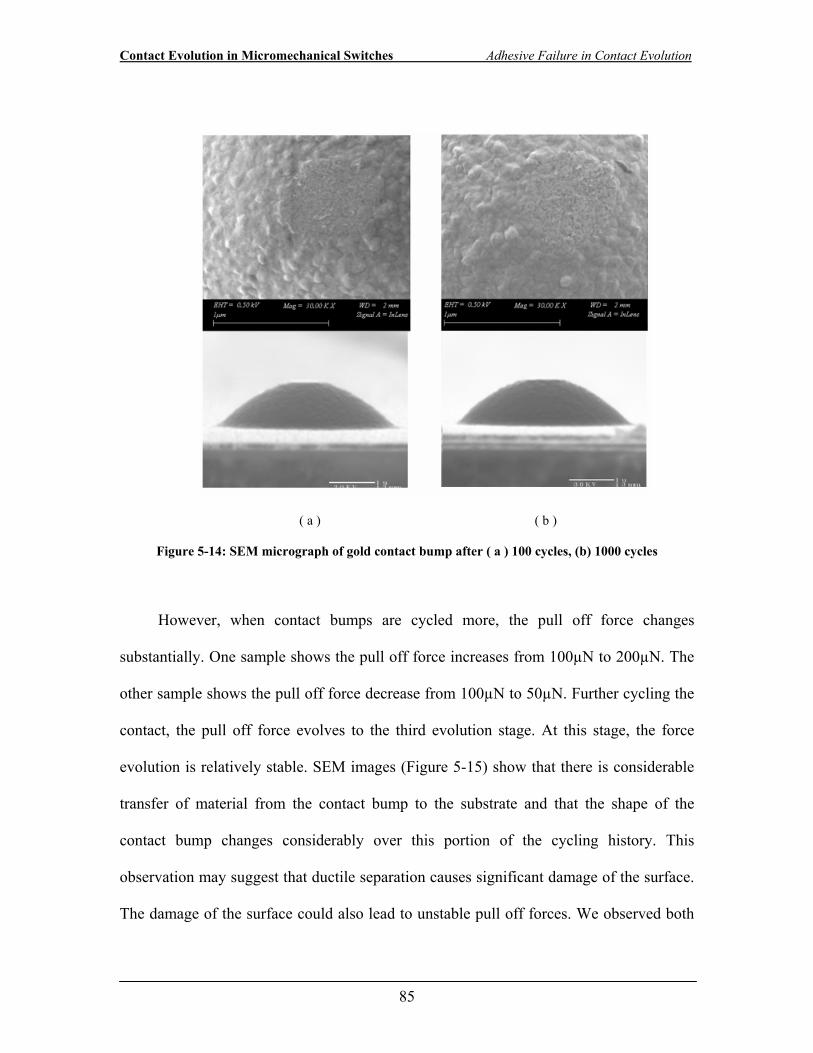
Contact Evolution in Micromechanical Switches Adhesive Failure in Contact Evolution
85
( a ) ( b )
Figure 5-14: SEM micrograph of gold contact bump after ( a ) 100 cycles, (b) 1000 cycles
However, when contact bumps are cycled more, the pull off force changes
substantially. One sample shows the pull off force increases from 100µN to 200µN. The
other sample shows the pull off force decrease from 100µN to 50µN. Further cycling the
contact, the pull off force evolves to the third evolution stage. At this stage, the force
evolution is relatively stable. SEM images (Figure 5-15) show that there is considerable
transfer of material from the contact bump to the substrate and that the shape of the
contact bump changes considerably over this portion of the cycling history. This
observation may suggest that ductile separation causes significant damage of the surface.
The damage of the surface could also lead to unstable pull off forces. We observed both
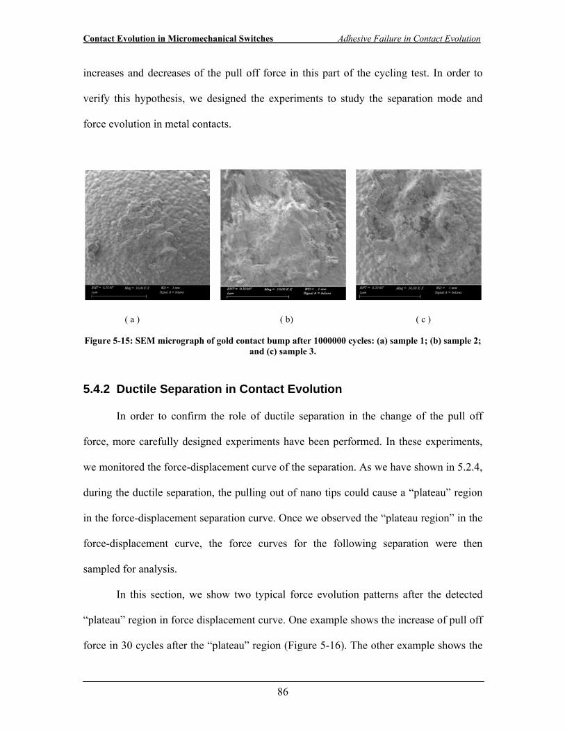
Contact Evolution in Micromechanical Switches Adhesive Failure in Contact Evolution
86
increases and decreases of the pull off force in this part of the cycling test. In order to
verify this hypothesis, we designed the experiments to study the separation mode and
force evolution in metal contacts.
( a ) ( b) ( c )
Figure 5-15: SEM micrograph of gold contact bump after 1000000 cycles: (a) sample 1; (b) sample 2; and (c) sample 3.
5.4.2 Ductile Separation in Contact Evolution
In order to confirm the role of ductile separation in the change of the pull off
force, more carefully designed experiments have been performed. In these experiments,
we monitored the force-displacement curve of the separation. As we have shown in 5.2.4,
during the ductile separation, the pulling out of nano tips could cause a “plateau” region
in the force-displacement separation curve. Once we observed the “plateau region” in the
force-displacement curve, the force curves for the following separation were then
sampled for analysis.
In this section, we show two typical force evolution patterns after the detected
“plateau” region in force displacement curve. One example shows the increase of pull off
force in 30 cycles after the “plateau” region (Figure 5-16). The other example shows the
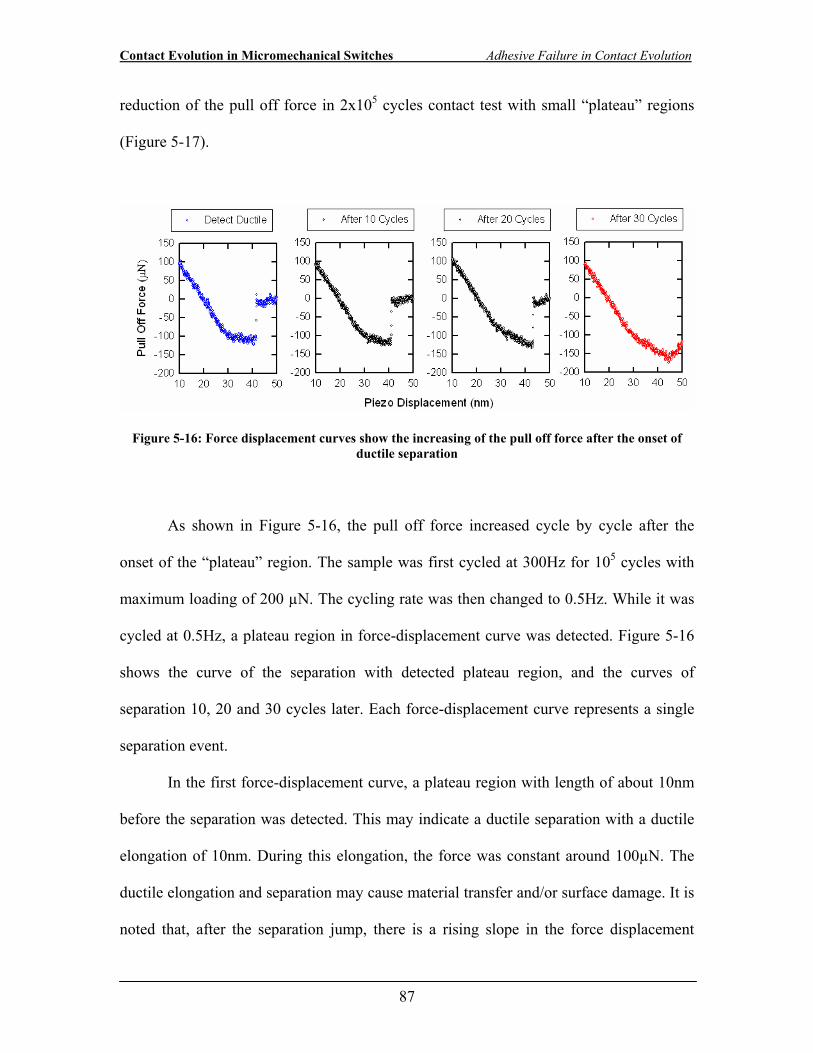
Contact Evolution in Micromechanical Switches Adhesive Failure in Contact Evolution
87
reduction of the pull off force in 2x10⁵ cycles contact test with small “plateau” regions
(Figure 5-17).
Figure 5-16: Force displacement curves show the increasing of the pull off force after the onset of ductile separation
As shown in Figure 5-16, the pull off force increased cycle by cycle after the
onset of the “plateau” region. The sample was first cycled at 300Hz for 105 cycles with
maximum loading of 200 µN. The cycling rate was then changed to 0.5Hz. While it was
cycled at 0.5Hz, a plateau region in force-displacement curve was detected. Figure 5-16
shows the curve of the separation with detected plateau region, and the curves of
separation 10, 20 and 30 cycles later. Each force-displacement curve represents a single
separation event.
In the first force-displacement curve, a plateau region with length of about 10nm
before the separation was detected. This may indicate a ductile separation with a ductile
elongation of 10nm. During this elongation, the force was constant around 100µN. The
ductile elongation and separation may cause material transfer and/or surface damage. It is
noted that, after the separation jump, there is a rising slope in the force displacement
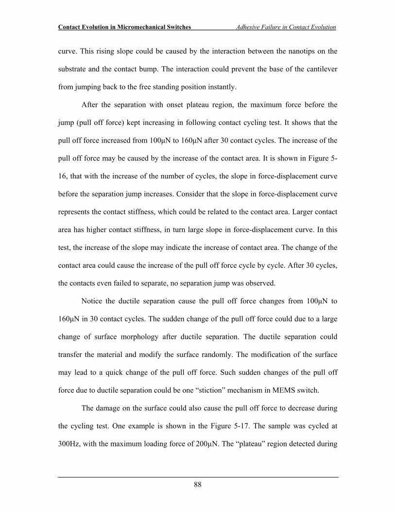
Contact Evolution in Micromechanical Switches Adhesive Failure in Contact Evolution
88
curve. This rising slope could be caused by the interaction between the nanotips on the
substrate and the contact bump. The interaction could prevent the base of the cantilever
from jumping back to the free standing position instantly.
After the separation with onset plateau region, the maximum force before the
jump (pull off force) kept increasing in following contact cycling test. It shows that the
pull off force increased from 100μN to 160μN after 30 contact cycles. The increase of the
pull off force may be caused by the increase of the contact area. It is shown in Figure 5-
16, that with the increase of the number of cycles, the slope in force-displacement curve
before the separation jump increases. Consider that the slope in force-displacement curve
represents the contact stiffness, which could be related to the contact area. Larger contact
area has higher contact stiffness, in turn large slope in force-displacement curve. In this
test, the increase of the slope may indicate the increase of contact area. The change of the
contact area could cause the increase of the pull off force cycle by cycle. After 30 cycles,
the contacts even failed to separate, no separation jump was observed.
Notice the ductile separation cause the pull off force changes from 100μN to
160μN in 30 contact cycles. The sudden change of the pull off force could due to a large
change of surface morphology after ductile separation. The ductile separation could
transfer the material and modify the surface randomly. The modification of the surface
may lead to a quick change of the pull off force. Such sudden changes of the pull off
force due to ductile separation could be one “stiction” mechanism in MEMS switch.
The damage on the surface could also cause the pull off force to decrease during
the cycling test. One example is shown in the Figure 5-17. The sample was cycled at
300Hz, with the maximum loading force of 200µN. The “plateau” region detected during
Contact Evolution in Micromechanical Switches Adhesive Failure in Contact Evolution
89
the cycling test is usually 2~3nm. For this sample, the pull off force reduced from 180μN
after first detecting of the “plateau” region in the force displacement curve, to 70μN after
5x10⁴ cycles contact. Between 5x10⁴ cycles contact and 2x10⁵ cycles contact, the
“plateau” area can still be detected; however, the magnitude of the pull off force changed
little.
Figure 5-17: Force displacement curves show the decreasing of the pull off force after the onset of ductile separation
The reduction of the pull off force could be due to the modification of the surface
after ductile fracture. During ductile separation, the material is pulled away from the
surfaces and smashed down by the following contact. The surfaces of the contact become
extremely rough after ductile separation; the real contact area will be reduced. At the
same time, the materials structure and properties may be different from the original
crystalline metals. During the pulling away as nanostructure, the gold surface could be
contaminated by the ambient. Both factors may contribute to the reduction of the pull off
force. After 5x10⁴ cycles contact, the force is stable, however, the ductile separation may
Contact Evolution in Micromechanical Switches Adhesive Failure in Contact Evolution
90
be still happening (with detectable “plateau” region). This observation may suggest the
ductile fracture could happen in small area without significantly change the force.
Both cases show the force change with detected “plateau” region in force
displacement curve, which is suspected to indicate the ductile separation. However,
cautions should be made here. The change of the contact area during the separation could
also change the slope in the force displacement curve. Since the slope of the force
displacement curve is corresponding to the contact stiffness, which is related to the
contact area. Large contact area has higher contact stiffness. Slowly decreasing of the
contact area could also lead to slowly change of contact stiffness, in turn, the change of
the slope. Thus, detected “plateau” region could also caused by a “slow” brittle
separation. However, in these two cases, the ductile separations were also confirmed by
the rising slope detected in force displacement curve after the jump. If the separation is
brittle, the force curve should be flat after the separation jump. However, due to the
ductile separation, material could be pulled away from the surface by 10~20nm. In turn,
there are may be still some interactions between the bump and the substrate, which could
prevent the base of cantilever from going back to the free standing position right after the
separation jump.
Based upon these observations, the magnitude of the pull off force could increase
or decrease after the ductile separation. The ductile separation could change contact area
or modify contact surface and cause the change of the pull off force instantly (less than
30 cycles contact). Or, small area of ductile separation may lead to the wear out of the
contact surfaces or contaminate the surface slowly and decrease the pull off force. Both
trends are commonly observed in our Au contact tests (more than 50 samples have been
Contact Evolution in Micromechanical Switches Adhesive Failure in Contact Evolution
91
tested). The same experiments have also been performed in both laboratory air and
nitrogen environments. No differences have been detected in force evolution features.
5.4.3 Modes Transition in Contact Evolution
An alternative method to determine the separation mode and contact evolution is
monitoring the rate dependent pull off force. Force-displacement separation curve could
provide a direct observation of the dynamics of the separation. However, the slope
change in the force-displacement of separation curve does not necessary indicate the
ductile separation. In addition, the ductile separation may not be able to generate a
detectable “plateau” region in the force-displacement curve. When the relaxation rate for
the ductile fracture is faster than the unloading speed, the plateau region may no be
detected. In this work, we found that the rate dependent pull off force could provide a
better sensitivity for identification of the separation modes.
5.4.3.1 Dominant separation modes
We identify the dominant separation mode by using rate dependent pull off force.
The pull off force is measured and compared at two cycling rate, 300Hz (F300) and 0.5Hz
(F05). Figure 5-18 shows the contact test results for contact evolution. The pull off force
data was sampled in a way that the sample was tested at 0.5Hz for 20~30 cycles and then
tested at 300Hz for 105 cycles. During the cycling test, the maximum pull off force is
controlled at 200µN. At each cycling rate, the pull off force was measured and the value
was averaged with 20 measurements. Figure 5-18 shows the measurement result of the
forces at different contact cycling stage.
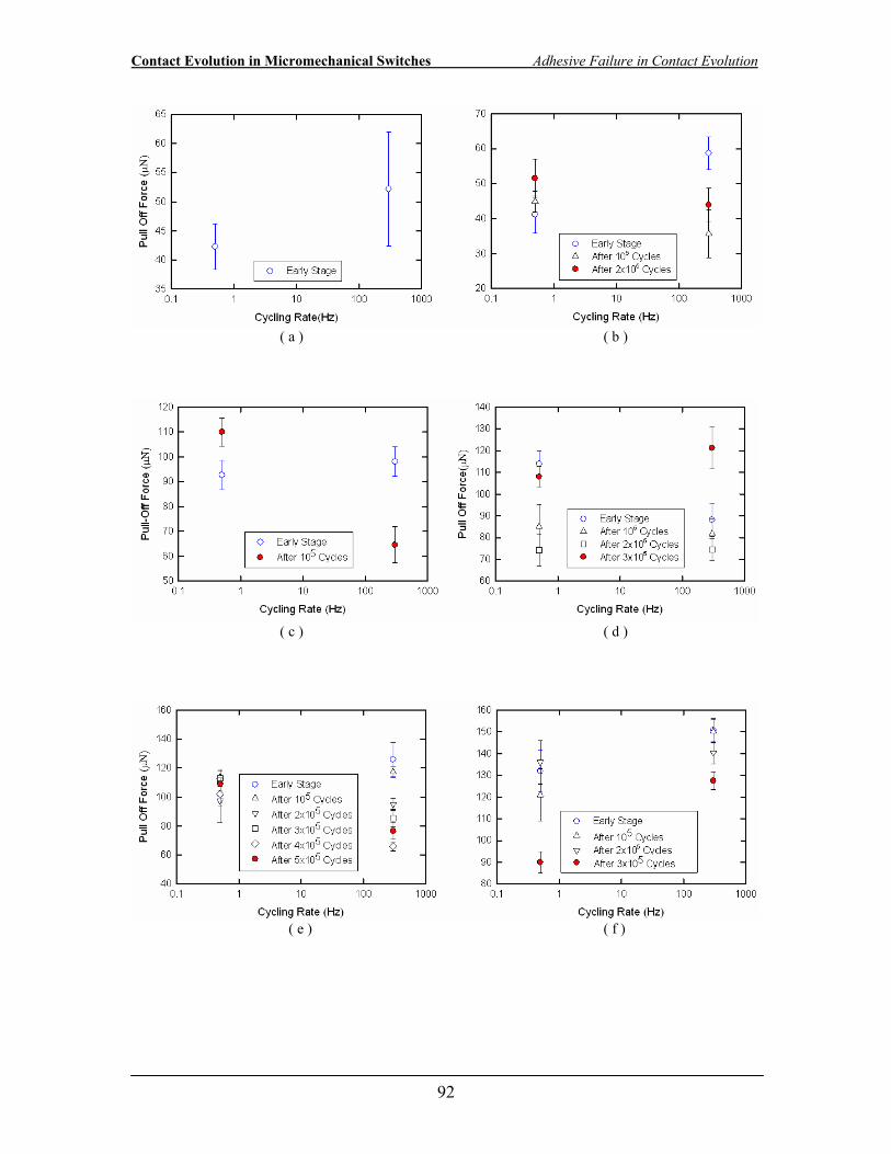
Contact Evolution in Micromechanical Switches Adhesive Failure in Contact Evolution
92
( a ) ( b )
( c ) ( d )
( e ) ( f )
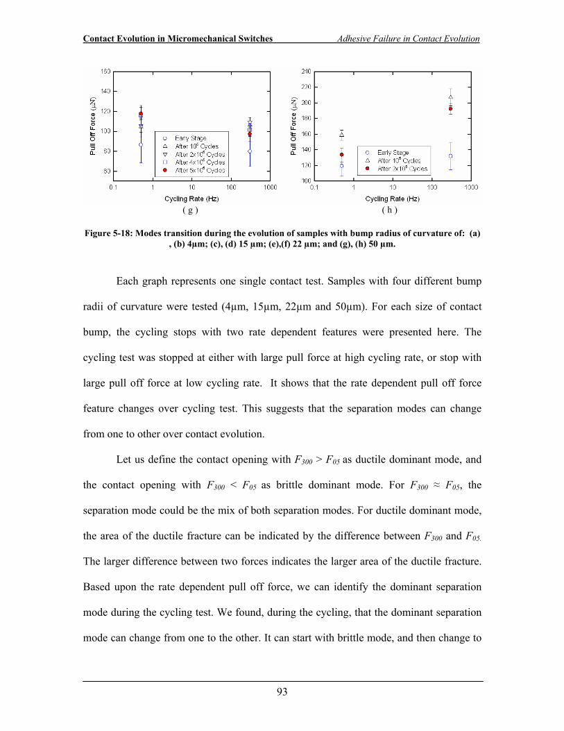
Contact Evolution in Micromechanical Switches Adhesive Failure in Contact Evolution
93
( g ) ( h ) Figure 5-18: Modes transition during the evolution of samples with bump radius of curvature of: (a)
, (b) 4µm; (c), (d) 15 µm; (e),(f) 22 µm; and (g), (h) 50 µm.
Each graph represents one single contact test. Samples with four different bump
radii of curvature were tested (4µm, 15µm, 22µm and 50µm). For each size of contact
bump, the cycling stops with two rate dependent features were presented here. The
cycling test was stopped at either with large pull force at high cycling rate, or stop with
large pull off force at low cycling rate. It shows that the rate dependent pull off force
feature changes over cycling test. This suggests that the separation modes can change
from one to other over contact evolution.
Let us define the contact opening with F300 > F05 as ductile dominant mode, and
the contact opening with F300 < F05 as brittle dominant mode. For F300 ≈ F05, the
separation mode could be the mix of both separation modes. For ductile dominant mode,
the area of the ductile fracture can be indicated by the difference between F300 and F05.
The larger difference between two forces indicates the larger area of the ductile fracture.
Based upon the rate dependent pull off force, we can identify the dominant separation
mode during the cycling test. We found, during the cycling, that the dominant separation
mode can change from one to the other. It can start with brittle mode, and then change to
Contact Evolution in Micromechanical Switches Adhesive Failure in Contact Evolution
94
a ductile dominant mode after cycling test (Figure 5-18 d). Or it starts with a small area
of ductile fracture, and then evolves to a large area of the ductile fracture (Figure 5-18 f,
h). After the ductile fracture, the separation mode can evolve back to brittle mode (Figure
5-18 c, e). Based upon the information of the separation mode, we then investigate how
the separation mode affects the force evolution in the micro contacts. One force evolution
curve with mode transitions are introduced in the following.
5.4.3.2 Force evolution in ductile to brittle mode
This section we show one example of force evolution and modes transition during
the cycling test. Figure 5-19 shows the pull off force evolution curve of the sample which
is tested up to 3x10⁵ cycles. It is observed, at the very beginning of the cycling test, the
force measured at 300Hz is significant larger than the value measured at the 0.5Hz. This
may due to large amount of plastic dissipation during a ductile separation. The plastic
dissipation can increase the pull off force during a fast unloading. Keep cycling the
contact, the pull off force measured at 0.5Hz starts to be in the same magnitude of the
force measured at 300Hz after 105 cycles. This may indicate the degree of plastic
dissipation is decreasing. The other evidence of changing dissipation can be found in the
force displacement curve. The separation mode may be the mixture of brittle and ductile.
Increasing the cycling number, the pull off force measured at 0.5Hz becomes larger than
the force measured at 300Hz. This observation may suggest the degree of the plastic
dissipation is further reduced. The separation mode becomes dominated by brittle mode.
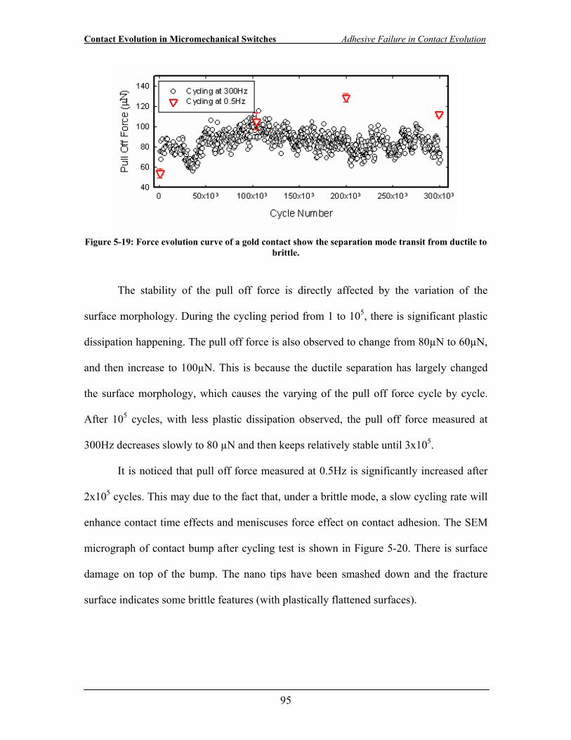
Contact Evolution in Micromechanical Switches Adhesive Failure in Contact Evolution
95
Figure 5-19: Force evolution curve of a gold contact show the separation mode transit from ductile to brittle.
The stability of the pull off force is directly affected by the variation of the
surface morphology. During the cycling period from 1 to 105, there is significant plastic
dissipation happening. The pull off force is also observed to change from 80µN to 60µN,
and then increase to 100µN. This is because the ductile separation has largely changed
the surface morphology, which causes the varying of the pull off force cycle by cycle.
After 105 cycles, with less plastic dissipation observed, the pull off force measured at
300Hz decreases slowly to 80 µN and then keeps relatively stable until 3x10⁵.
It is noticed that pull off force measured at 0.5Hz is significantly increased after
2x10⁵ cycles. This may due to the fact that, under a brittle mode, a slow cycling rate will
enhance contact time effects and meniscuses force effect on contact adhesion. The SEM
micrograph of contact bump after cycling test is shown in Figure 5-20. There is surface
damage on top of the bump. The nano tips have been smashed down and the fracture
surface indicates some brittle features (with plastically flattened surfaces).
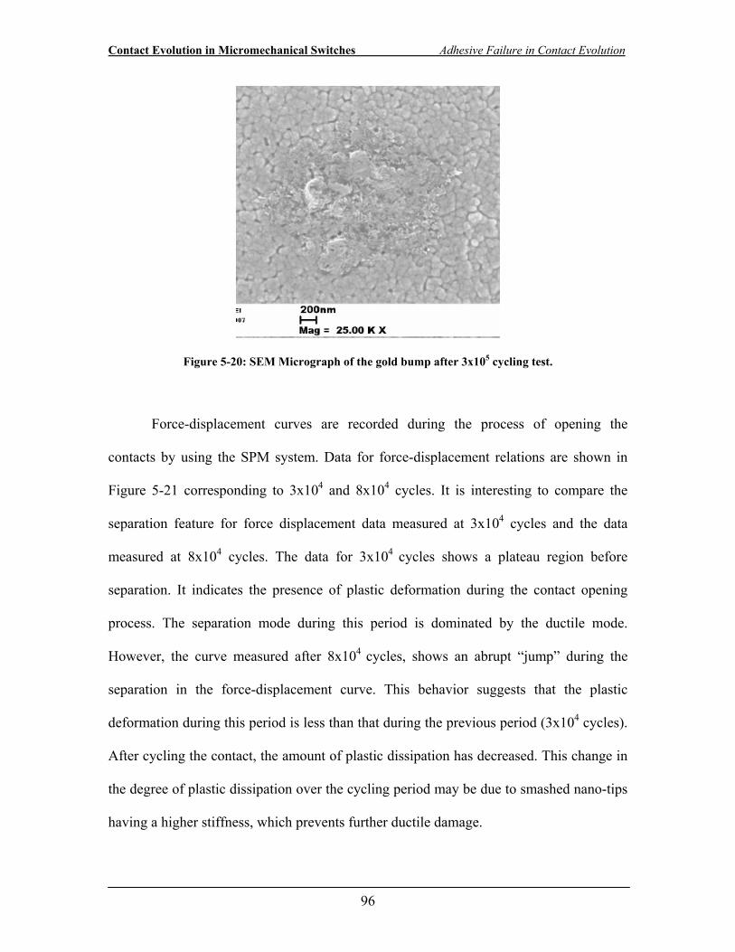
Contact Evolution in Micromechanical Switches Adhesive Failure in Contact Evolution
96
Figure 5-20: SEM Micrograph of the gold bump after 3x10⁵ cycling test.
Force-displacement curves are recorded during the process of opening the
contacts by using the SPM system. Data for force-displacement relations are shown in
Figure 5-21 corresponding to 3x10⁴ and 8x10⁴ cycles. It is interesting to compare the
separation feature for force displacement data measured at 3x10⁴ cycles and the data
measured at 8x10⁴ cycles. The data for 3x10⁴ cycles shows a plateau region before
separation. It indicates the presence of plastic deformation during the contact opening
process. The separation mode during this period is dominated by the ductile mode.
However, the curve measured after 8x10⁴ cycles, shows an abrupt “jump” during the
separation in the force-displacement curve. This behavior suggests that the plastic
deformation during this period is less than that during the previous period (3x10⁴ cycles).
After cycling the contact, the amount of plastic dissipation has decreased. This change in
the degree of plastic dissipation over the cycling period may be due to smashed nano-tips
having a higher stiffness, which prevents further ductile damage.
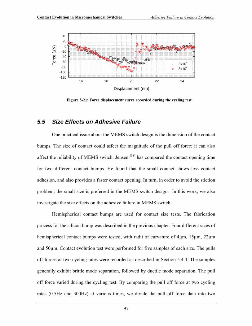
Contact Evolution in Micromechanical Switches Adhesive Failure in Contact Evolution
97
Displacement (nm)
16 18 20 22 24
Forc
e (μΝ)
-120-100-80-60-40-20
02040
3x10⁴
8x10⁴
Figure 5-21: Force displacement curve recorded during the cycling test.
5.5 Size Effects on Adhesive Failure
One practical issue about the MEMS switch design is the dimension of the contact
bumps. The size of contact could affect the magnitude of the pull off force; it can also
affect the reliability of MEMS switch. Jensen [18] has compared the contact opening time
for two different contact bumps. He found that the small contact shows less contact
adhesion, and also provides a faster contact opening. In turn, in order to avoid the stiction
problem, the small size is preferred in the MEMS switch design. In this work, we also
investigate the size effects on the adhesive failure in MEMS switch.
Hemispherical contact bumps are used for contact size tests. The fabrication
process for the silicon bump was described in the previous chapter. Four different sizes of
hemispherical contact bumps were tested, with radii of curvature of 4µm, 15µm, 22µm
and 50µm. Contact evolution test were performed for five samples of each size. The pulls
off forces at two cycling rates were recorded as described in Section 5.4.3. The samples
generally exhibit brittle mode separation, followed by ductile mode separation. The pull
off force varied during the cycling test. By comparing the pull off force at two cycling
rates (0.5Hz and 300Hz) at various times, we divide the pull off force data into two
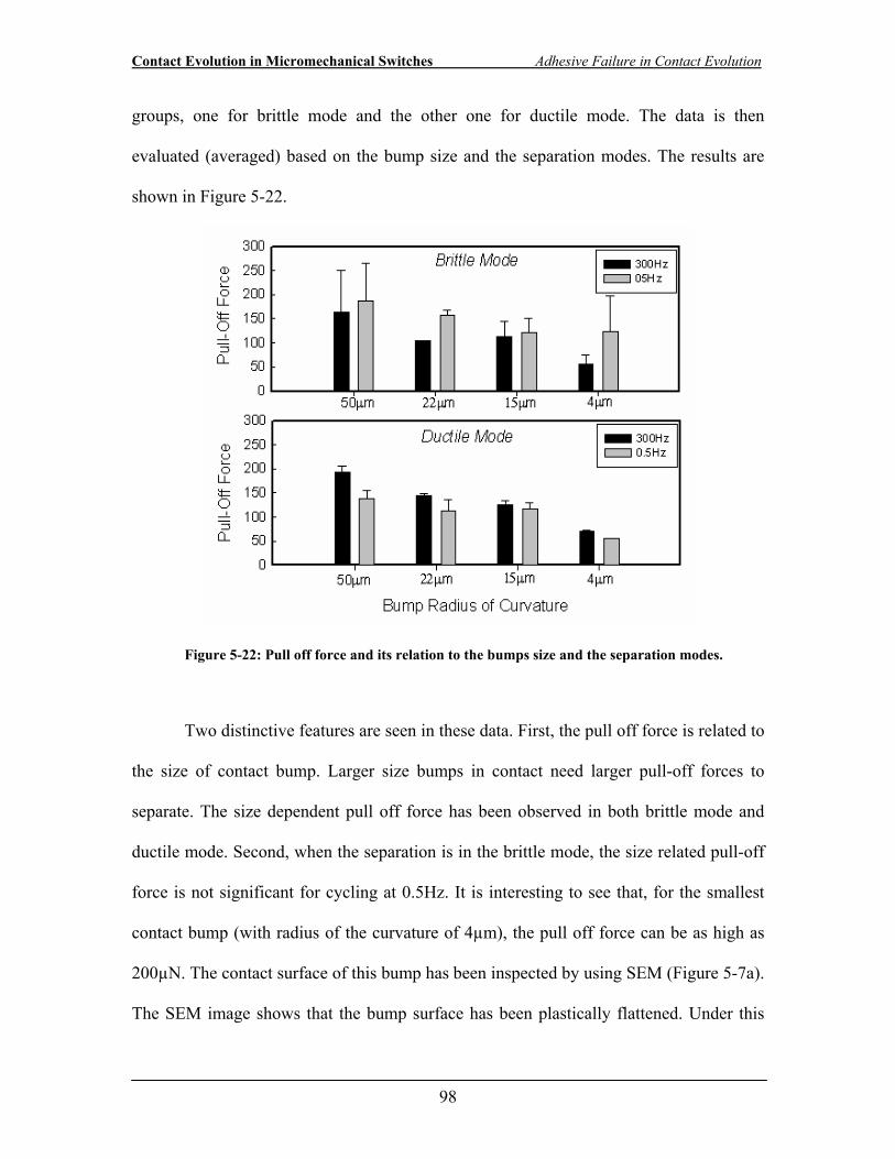
Contact Evolution in Micromechanical Switches Adhesive Failure in Contact Evolution
98
groups, one for brittle mode and the other one for ductile mode. The data is then
evaluated (averaged) based on the bump size and the separation modes. The results are
shown in Figure 5-22.
Figure 5-22: Pull off force and its relation to the bumps size and the separation modes.
Two distinctive features are seen in these data. First, the pull off force is related to
the size of contact bump. Larger size bumps in contact need larger pull-off forces to
separate. The size dependent pull off force has been observed in both brittle mode and
ductile mode. Second, when the separation is in the brittle mode, the size related pull-off
force is not significant for cycling at 0.5Hz. It is interesting to see that, for the smallest
contact bump (with radius of the curvature of 4µm), the pull off force can be as high as
200µN. The contact surface of this bump has been inspected by using SEM (Figure 5-7a).
The SEM image shows that the bump surface has been plastically flattened. Under this
Contact Evolution in Micromechanical Switches Adhesive Failure in Contact Evolution
99
condition, the two contact surfaces are conformal to each other, which make the contact
susceptible to surface force, such as meniscus force effect. As shown before, time in
contact could affect the magnitude of the surface. Hence, a large pull off force could be
needed at a slow cycling rate.
In conclusion, the size does affect the magnitude of the pull off force. For large
bumps, the pull off force is usually larger. For gold contact, both separation modes have
been observed in four bump size. The maximum detected pull off force seems to happen
at a slow brittle separation.
5.6 Material Effects on Adhesive Failure
Material properties have a strong effect on adhesive failure in MEMS switch. For
instance, “stiction” problem is often observed in gold contact MEMS switch [17]. Large
adhesion in gold contacts is due to their low hardness and inert surface. Soft gold contact
is easy to deform to a large conformal surface which results in a large contact adhesion.
Also, the low hardness and inert surface could make gold contact susceptible to the
ductile separation. As we have shown, the ductile separation can cause large scatter of
pull off force, which leads to unstable performance in gold contact MEMS switch. In our
test, the pull-off force for gold contacts has been observed to vary from 50µN to 200 µN
during cycling tests.
In order to avoid large adhesion, as well as ductile separation, choosing
alternative contact materials could be the solution. In this work, we study the contact
evolution features of Au-5%Ru. The Au-5%Ru was prepared by using DC magnetron
sputtering with a nominal thickness of 300nm. The material was deposited on three
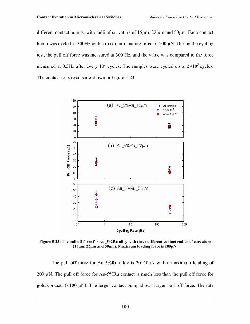
Contact Evolution in Micromechanical Switches Adhesive Failure in Contact Evolution
100
different contact bumps, with radii of curvature of 15µm, 22 µm and 50µm. Each contact
bump was cycled at 300Hz with a maximum loading force of 200 µN. During the cycling
test, the pull off force was measured at 300 Hz, and the value was compared to the force
measured at 0.5Hz after every 105 cycles. The samples were cycled up to 2×10⁵ cycles.
The contact tests results are shown in Figure 5-23.
Figure 5-23: The pull off force for Au_5%Ru alloy with three different contact radius of curvature (15µm, 22µm and 50µm). Maximum loading force is 200µN.
The pull off force for Au-5%Ru alloy is 20~50µN with a maximum loading of
200 µN. The pull off force for Au-5%Ru contact is much less than the pull off force for
gold contacts (~100 µN). The larger contact bump shows larger pull off force. The rate
Contact Evolution in Micromechanical Switches Adhesive Failure in Contact Evolution
101
dependent pull off force measurement shows that the force measured at 0.5Hz was
always larger than the force measured at 300Hz. This rate related feature indicates brittle
separation during the cycling test. SEM inspection also shows that there is no material
transfer observable after the 2x10⁵ cycle test. This set of experiments show that 5
atomic% Ru in a gold thin film can significantly lower the pull off force, reducing the
chances of ductile separation.
The different magnitude of the pull off force between Au-5%Ru and Au contacts
could be due to the alloy effects from Ru. It is found that the measured hardness for
Au_5%Ru thin film (2.42GPa) is about two times higher than the hardness of gold thin
film (1.04GPa) (Table 6-1). The 5% Ru in the gold film may provide dislocation
obstacles, which can help to increase the hardness. At the same time, the Ru could disturb
the electron structures on the gold surface, which may weaken the interfacial energy and
lead to brittle separation. The effect of adding Ru to Au thin film could be similar to the
embrittlement effect in Bi-Cu [73], and Mg-Al [74] system. It is found that the segregation
of Bi or Mg at the grain boundary can significant lower boundary bonding strength,
which cause the fracture mode of Cu and Al changes from ductile to brittle. The
embrittlement mechanisms could be either due to that the segregation Bi atoms push
apart the Cu atoms at the interface and weaken the inter-atomic bonding [73]; or due to Mg
atoms form weaker cohesive bonding with Al than the bonding Al-Al [74]. These
impurities effects can decrease the cohesive strength at the interface and facilitate brittle
fracture.
Other hard metals, such as ruthenium (Ru), rhodium (Rh) and platinum (Pt), and
some of their alloys with gold (Au) were also tested. The preparation of these materials
Contact Evolution in Micromechanical Switches Adhesive Failure in Contact Evolution
102
and their contact resistance performance will be discussed in next Chapter. In general, for
materials with a higher hardness, the extent of ductile separation and pull off force is
greatly reduced. The pull off force is barely detected in our force measurement system
with resolution of 10~15 µN. The reduction of the pull off force could due to their higher
hardness and contaminated surfaces. Failure mechanisms of hard materials will be
discussed in details in Chapter 6.
5.7 Conclusions
We have studied the separation modes in Au/Au contacts and their roles in
adhesive failure during contact evolution. When the gold surfaces are covered with a
layer of surface film, the separation of the contact is in a brittle mode. There is no or little
material transfer during the separation. However, when the gold surfaces are clean,
ductile separation can occur after a single load-unload cycle. In such cases, the separation
can generate elongated nano-tips on the surface. Two separation modes have different
opening dynamics; in turn they have different stiction mechanisms in the real MEMS
switches operations.
In the brittle separation mode, the pull off force measured at low cycling rates is
larger than the force measured at high cycling rate. The rate dependent pull off force in
the brittle mode may be related to kinetics of the surface events. For hydrophilic surfaces,
such as gold, the surface events could be meniscus condensation and/or surface wetting in
the ambient. For conforming gold contacts, the meniscus force induced adhesion can be
one stiction mechanism in the MEMS switches.
Contact Evolution in Micromechanical Switches Adhesive Failure in Contact Evolution
103
During ductile separation, the generation of the ductile tips can cause viscous
effect during the separation. The viscous effects cause a larger pull off force at high
cycling rates than at low cycling rates. The magnitude of the pull off force is related to
the ductile area. The larger the area of ductile fracture that is activated, the larger the pull
off force that is needed to separate the contacts. Continued loading after ductile
separation will flatten out the sharp tips while creating new stretched tips during
unloading. Many thousands of loading and unloading cycles can change the roughness
and stiffness of the contact surfaces. Since the surface morphology is randomly modified
due to many ductile separations, the pull-off force changes showing significant scatter.
Since gold is intrinsically ductile, adhesive failure due to the ductile separation could be
the major reliability issue. In the real gold contact operation, the ductile separation can
cause the problems such as: sluggish contact opening, stiction and contact wear.
In general, the separation of the contact is in a mixed mode, including both brittle
and ductile separation. Based on the rate related pull off force properties, the dominant
separation modes can be identified during the cycling test. For contacts with a layer of
surface film, the separation could start with a brittle dominant mode, which then turns to
the ductile dominant after cycling. Ductile separation will initiate a large degree of plastic
dissipation which decreases during the cycling test. The separation mode can turn back to
brittle dominant after thousands of cycles. This evolution characteristic may be due to the
variation of material properties which can inhibit further ductile separation.
Since ductile separation can cause an unstable pull off force, and material transfer,
in order to design reliable MEMS switches, the ductile separation should be avoided. For
gold contacts, ductile separation has been observed in four different sizes of the contact
Contact Evolution in Micromechanical Switches Adhesive Failure in Contact Evolution
104
bumps. This is probably due to the fact that material properties are dominant in causing
the separation to be ductile. The large contact bump will need a large pull off force to
separate. When contact surfaces are plastically deformed, slow separation in brittle mode
could cause large pull off force. By introducing 5 atomic % of Ru into the gold thin film,
the pull off force is reduced by about 60%, and the separation characteristics and SEM
micrographs show only brittle features. Selection of alternative contact materials could be
a good solution for reliable operation of MEMS switches.
Contact Evolution in Micromechanical Switches Contamination Failure in Contact Evolution
105
6 Contamination Failure in Contact Evolution
6.1 Introduction
Contact resistance is a critical parameter in MEMS switch design. In order to
handle more power and reduce losses, low contact resistance is preferred. The value of
contact resistance depends on contact force, contact geometry, surface condition and
contact material. For a perfectly clean contact, material properties, i.e. hardness and
electrical resistivity, determine resistance for a given contact force. Generally, the
constriction resistance for a single-asperity contact between two half-spaces, with contact
radius significantly larger than the mean free path for electrons, is given by [75]
a
Rc 2ρ
= (Equation 6-1)
where ρ is the electrical resistivity of metal and a is the radius of the contact spot
(assumed to be circular). However, with a surface film interposed between the contacts,
the contact resistance should include a contribution from the surface film. The film
resistance Rf can be expressed as [76]:
2ad
R ff ⋅
⋅=πρ
(Equation 6-2)
Contact Evolution in Micromechanical Switches Contamination Failure in Contact Evolution
106
where fρ is the film electrical resistivity and d is the thickness of the film. The contact
resistance is approximately the sum of the constriction resistance and the film resistance.
As we can see from above, the resistance value is related to the contact size, metal
electrical resistivity, surface film electrical resistivity and surface film thickness. In order
to reach a desired contact resistance, contact force need be large enough to reduce the
film resistance. One of reliability problems in real life operation of MEMS switches is
increases in the resistance. Buildup of contamination will increase the resistance during
cycling, and cause high resistance failure (“fail to close”). Development of contamination
layers on the surfaces is related to the contaminants present on or around the contacts and
to the material properties. Different contact materials have different contamination
features.
Gold surfaces are known to be relatively inert to contamination. Gold contacts
have been widely used in metal contact MEMS switch design. In addition to their
inertness, low hardness and high conductivity make Au very suitable for low force
applications. However, as we have shown in Chapter 5, soft gold contacts are susceptible
to contact wear and adhesive failure. In order to overcome this problem, researchers are
working on finding harder materials for better reliability performance. Schimkat [14] used
a piezo-controlled contact testing system to evaluate contact materials (Au, Au-5%Ni and
Rh). He suggested that Au-5%Ni and Rh, with a lower adherence force than Au, may be
better candidates for MEMS switch design. Majumder et al. [4] reported that a “platinum
group” metal contact can be reliably cycled up to 1011 times under cold switching
conditions. Coutu et al. [24] tested Au-6.3%Pt contacts up to 2.7×10⁸ cycles under “hot-
switch” conditions. All of these works indicate that noble metals or some Au alloy may
Contact Evolution in Micromechanical Switches Contamination Failure in Contact Evolution
107
provide better candidate materials for contact MEMS switches.
In the pursuit of determining desirable contact materials for RF MEMS switches,
we investigated the contact resistance of three noble metals (Pt, Rh, Ru) and their alloys
with Au. The thin films for contact tests were deposited using DC magnetron sputtering
and the hardness of the films was measured by instrumented nanoindentation. The
contact resistances are measured by specially designed SPM-based setup. The contact
resistance results are correlated with resistivity, hardness, and elastic modulus obtained
from nanoindentation testing. The reliability performance of different contact materials is
also evaluated by cycling contacts and monitoring the evolution of contact resistance.
The buildup rate of contamination is indicated by the increase of contact resistance.
Contact materials with different surface reactivity show distinctive contact resistance
evolution characteristics. It is expected that these results may provide guidelines and
improved understanding of the electrical contact materials for RF MEMS switches.
6.2 Nobleness of Gold and Gold-Alloys
6.2.1 Film Preparation [77]
Thin films having a nominal thickness of 300 nm were deposited on silicon
substrates from 99.95% pure Au, Pt, Rh, and Ru in a Denton Vacuum Discovery 18 dc
magnetron sputtering system with a base vacuum of 1.4 x 10⁻⁶ Pa. A mass-flow regulated
Ar sputtering pressure of 0.32 Pa was used for all depositions except for Pt depositions at
1.06 Pa. Substrate materials were 75 mm diameter and 380 μm thick (100) silicon disk
wafers. Substrates were cleaned in a buffered oxide etch solution, nitrogen dried and Ar
Contact Evolution in Micromechanical Switches Contamination Failure in Contact Evolution
108
plasma cleaned for 5 minutes at 60 W prior to deposition. Table 6-1 (b) shows the alloys
studied, deposition rates, and cathode powers to achieve the alloy films.
Table 6-1: (a) Hardness, modulus and resistiviy; (b) deposition power and rate; for single metal and co-sputtered metal films.
( a ) ( b ) Hardness
(GPa) Modulus
(GPa) Resistivity
(µΩ.m) Power (W)
Deposition Rate (nm/min)
Au 1.04 86 3.6 250 87
Pt 5.39 183 16.6 250 48
Rh 9.75 256 9.3 250 40
Ru 15.28 295 13.8 250 27
Au-30%Rh 4.87 153 58.8 250/254 126
Au-70%Rh 9.57 217 44 47/250 57
Au-5%Ru 2.42 122 38.5 250/56 95
Au-10%Ru 3.99 137 56.5 250/103 101
Au-20%Ru 4.28 148 69.9 250/197 104
Au-30%Ru 6.18 154 87 168/250 87
Au-70%Ru 11.46 231 86 33/250 39
Au-10%Pt 2.79 124 15.2 250/54 95
Au-50%Pt 5.1 155 47.2 127/250 87
Note: The values were measured at 24nm indentation for 300nm thickness film using a Nanoindenter XP from MTS (Oak Ridge, TN). Deposition rate for alloys is cumulative for both targets. Sputter power for alloys is noted as Au power/metal power.
Nanoindentation tests were conducted using a Nanoindenter XP (MTS system,
Oak Ridge, TN) with a Berkovich tip using a Dynamic Contact Module (DCM) which
has displacement and load resolutions of 0.5nm and 2nN in air, respectively. A total of
the fifteen indentations were conducted on each specimen using the continuous stiffness
Contact Evolution in Micromechanical Switches Contamination Failure in Contact Evolution
109
measurement (CSM) technique [78]; the average values of these fifteen indentations are
presented in the present study. Film resistivity was calculated from the sheet resistance
measured by a standard four-point probe and the film thickness was measured using a
profilemeter. At least ten resistivity measurements were obtained across each of the thin
film wafers to ensure uniform material deposition.
Table 6-1 (a) shows the hardness and elastic modulus of thin films of three metals
(Pt, Rh, Ru) and gold along with their alloys. The hardness values were taken at a 24 nm
indentation depth (i.e. a depth 8% of the film thickness). Compared to pure Au, the other
noble metals have higher hardnesses and elastic moduli. By alloying Au with noble
metals, both the hardness and elastic modulus are increased. The hardening effects of
alloying elements may be due to the presence of these foreign phases or atoms which
serve as dislocation obstacles, thus increasing the mechanical strength of the Au thin
film. However, the resistivity of the alloys is significantly higher than of the pure metals.
6.2.2 Contact Resistance
6.2.2.1 Resistance measurement
Contact resistance and its characteristics are studied by SPM based contact tester.
As shown in Figure 6-1 (a), the contact bumps are approximately 2.5 μm in diameter and
1 μm tall and were fabricated on top of a cantilever (Figure 6-1 (b)) using a silicon
micromachining process. The bumps are made by wet etching a 1μm thick thermally
grown silicon oxide layer using a buffered oxide etch solution. Contact was made using a
piezoelectric actuator mounted on the SPM stage to press a flat substrate against the
Contact Evolution in Micromechanical Switches Contamination Failure in Contact Evolution
110
contact bump of the cantilever. The size of the silicon cantilevers is 80 x 30 x 180μm
with a spring constant of about 1.5 x 10⁴ N/m, which was estimated from the measured
dimensions of the cantilever. A schematic of the experimental apparatus is shown in
Chapter 4. The contact force is proportional to the magnitude of the deflection, which is
obtained from the optical system of the SPM and the spring constant of the test
cantilevers. The contact force was controlled by the displacement of the piezoelectric
actuator and monitored by the deflection of the cantilever. Using this setup, it was
possible to maintain a contact force in the range of 200–250µN with a resolution of 25µN
in each test. Contact tests were performed between contact pairs of the same deposited
material. Contact resistance evolution characteristics were studied by cycling the contact
in a cold switching mode (voltage is only placed across the contacts when the surfaces
are in contact).
A source meter (2410, Keithley Instruments, Cleveland, OH) was used for four-
wire contact resistance measurements with a 1mA current source and a 2.1V compliance
voltage. Figure 6-1 (c, d) shows the structure layout for the four-wire resistance
measurement. There are four probes – two probes are attached to the cantilever and the
other two probes are attached to the substrate. On the cantilever side, two testing probes
are placed at the end of the cantilever. The sheet resistance from the metal thin film on
the cantilever will be inevitably included in the measurement. On the substrate side, a
voltage probe and a current probe are located separately on two opposite sides of the
substrate as shown in the Figure 6-1(c). The contact area is located near the edge of the
third side. This arrangement of contact probe greatly reduces the sheet resistance
component from the substrate. Contact resistance measurements were done on as-
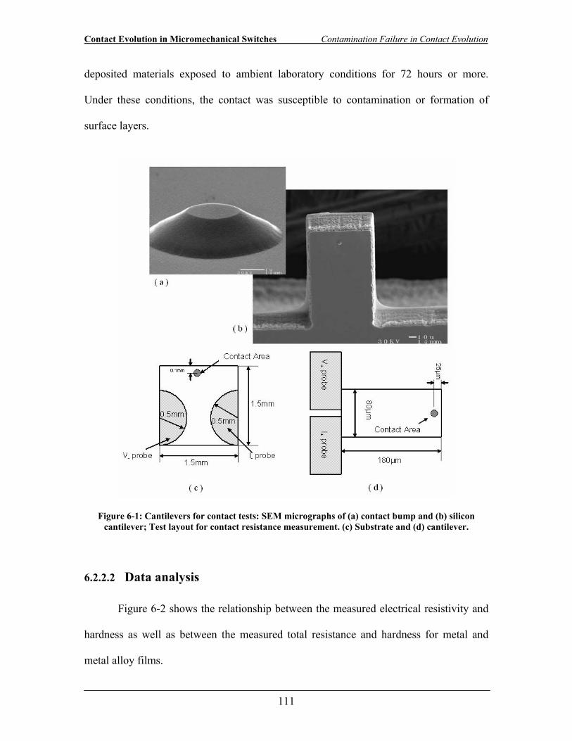
Contact Evolution in Micromechanical Switches Contamination Failure in Contact Evolution
111
deposited materials exposed to ambient laboratory conditions for 72 hours or more.
Under these conditions, the contact was susceptible to contamination or formation of
surface layers.
Figure 6-1: Cantilevers for contact tests: SEM micrographs of (a) contact bump and (b) silicon cantilever; Test layout for contact resistance measurement. (c) Substrate and (d) cantilever.
6.2.2.2 Data analysis
Figure 6-2 shows the relationship between the measured electrical resistivity and
hardness as well as between the measured total resistance and hardness for metal and
metal alloy films.
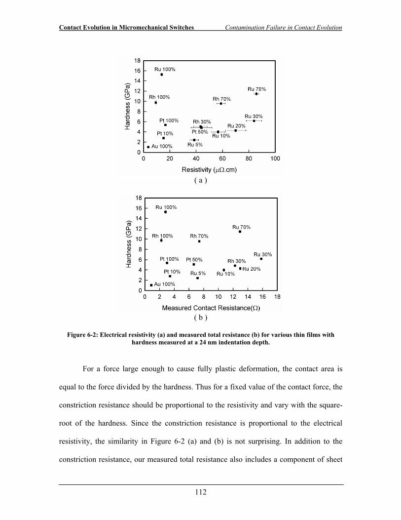
Contact Evolution in Micromechanical Switches Contamination Failure in Contact Evolution
112
( a )
( b )
Figure 6-2: Electrical resistivity (a) and measured total resistance (b) for various thin films with hardness measured at a 24 nm indentation depth.
For a force large enough to cause fully plastic deformation, the contact area is
equal to the force divided by the hardness. Thus for a fixed value of the contact force, the
constriction resistance should be proportional to the resistivity and vary with the square-
root of the hardness. Since the constriction resistance is proportional to the electrical
resistivity, the similarity in Figure 6-2 (a) and (b) is not surprising. In addition to the
constriction resistance, our measured total resistance also includes a component of sheet
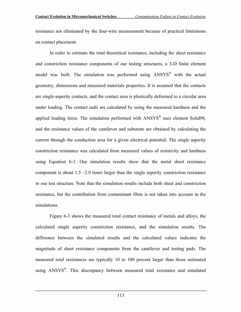
Contact Evolution in Micromechanical Switches Contamination Failure in Contact Evolution
113
resistance not eliminated by the four-wire measurement because of practical limitations
on contact placement.
In order to estimate the total theoretical resistance, including the sheet resistance
and constriction resistance components of our testing structures, a 3-D finite element
model was built. The simulation was performed using ANSYS® with the actual
geometry, dimensions and measured materials properties. It is assumed that the contacts
are single-asperity contacts, and the contact area is plastically deformed to a circular area
under loading. The contact radii are calculated by using the measured hardness and the
applied loading force. The simulation performed with ANSYS® uses element Solid98,
and the resistance values of the cantilever and substrate are obtained by calculating the
current through the conduction area for a given electrical potential. The single asperity
constriction resistance was calculated from measured values of resistivity and hardness
using Equation 6-1. Our simulation results show that the metal sheet resistance
component is about 1.5 –2.0 times larger than the single asperity constriction resistance
in our test structure. Note that the simulation results include both sheet and constriction
resistance, but the contribution from contaminant films is not taken into account in the
simulations.
Figure 6-3 shows the measured total contact resistance of metals and alloys, the
calculated single asperity constriction resistance, and the simulation results. The
difference between the simulated results and the calculated values indicates the
magnitude of sheet resistance components from the cantilever and testing pads. The
measured total resistances are typically 10 to 100 percent larger than those estimated
using ANSYS®. This discrepancy between measured total resistance and simulated
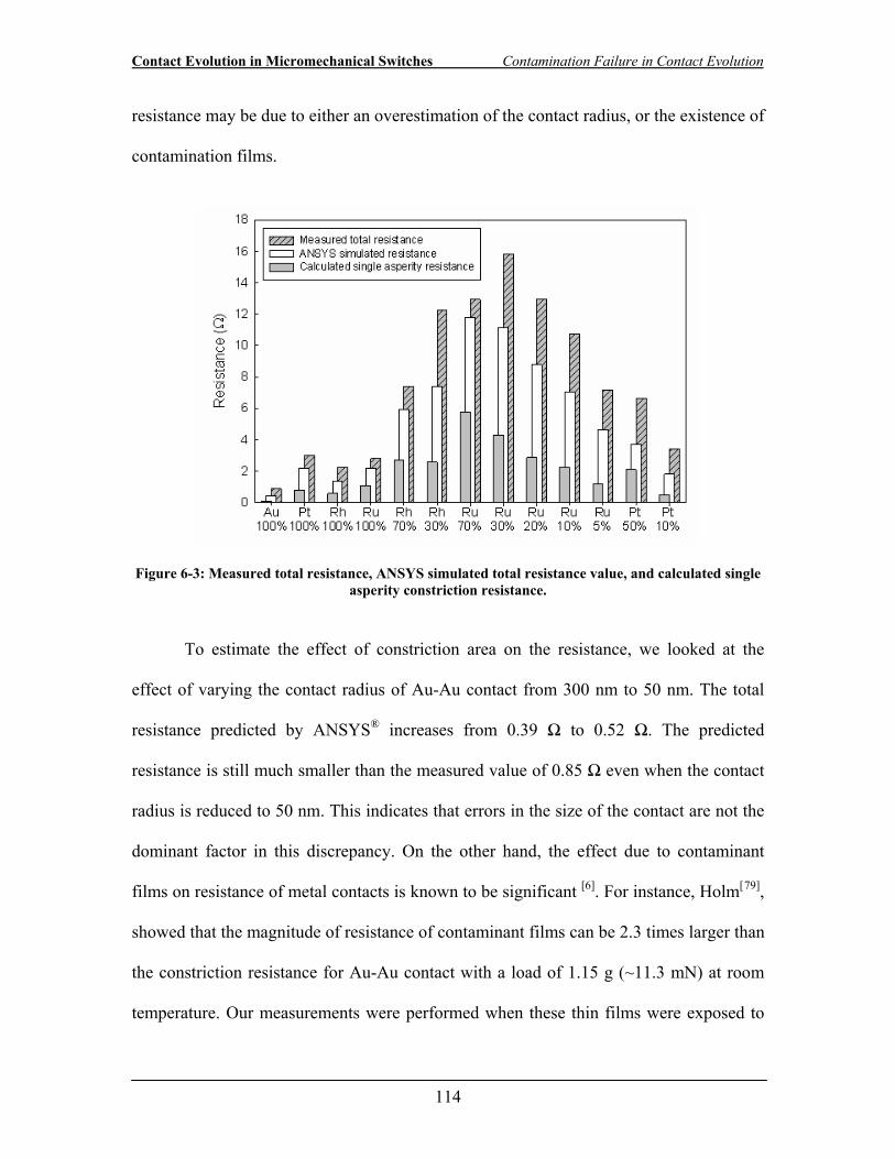
Contact Evolution in Micromechanical Switches Contamination Failure in Contact Evolution
114
resistance may be due to either an overestimation of the contact radius, or the existence of
contamination films.
Figure 6-3: Measured total resistance, ANSYS simulated total resistance value, and calculated single asperity constriction resistance.
To estimate the effect of constriction area on the resistance, we looked at the
effect of varying the contact radius of Au-Au contact from 300 nm to 50 nm. The total
resistance predicted by ANSYS® increases from 0.39 Ω to 0.52 Ω. The predicted
resistance is still much smaller than the measured value of 0.85 Ω even when the contact
radius is reduced to 50 nm. This indicates that errors in the size of the contact are not the
dominant factor in this discrepancy. On the other hand, the effect due to contaminant
films on resistance of metal contacts is known to be significant [6]. For instance, Holm[79],
showed that the magnitude of resistance of contaminant films can be 2.3 times larger than
the constriction resistance for Au-Au contact with a load of 1.15 g (~11.3 mN) at room
temperature. Our measurements were performed when these thin films were exposed to
Contact Evolution in Micromechanical Switches Contamination Failure in Contact Evolution
115
ambient laboratory conditions for 72 hours or more. Therefore, the resistance due to
contamination films may have a significant contribution to the measured resistance.
Figure 6-4: The ratio of the ANSYS simulated resistance to the measured total resistance for various thin films.
In addition, in Figure 6-4, we plot the ratio of the ANSYS® simulated resistance
(constriction resistance and sheet resistance) to the measured total contact resistance vs.
the hardness. The harder materials typically show a higher ratio of predicted to measured
resistance values. This observation may indicate that the surface films or contamination
layers are less important in the harder materials. This may due to the fact that harder
material may more easily break or squeeze out the surface contaminant films than the
softer materials. However, there will often be more than one asperity contact in metal
contacts. Harder materials are less likely to form single asperity contacts than the more
easily deformable softer materials. Thus the single asperity assumption may be less valid
for the harder materials. For N asperities in contact, all plastically deforming, the average
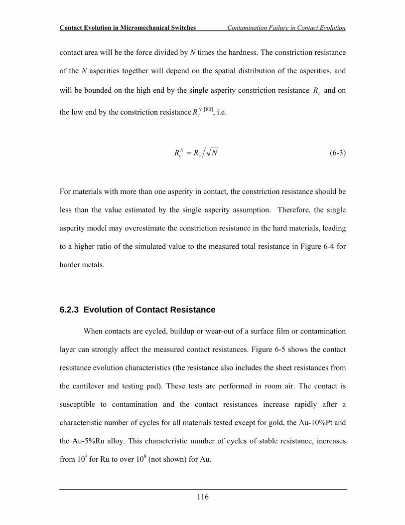
Contact Evolution in Micromechanical Switches Contamination Failure in Contact Evolution
116
contact area will be the force divided by N times the hardness. The constriction resistance
of the N asperities together will depend on the spatial distribution of the asperities, and
will be bounded on the high end by the single asperity constriction resistance cR and on
the low end by the constriction resistance NcR [80], i.e.
NRR cNc = (6-3)
For materials with more than one asperity in contact, the constriction resistance should be
less than the value estimated by the single asperity assumption. Therefore, the single
asperity model may overestimate the constriction resistance in the hard materials, leading
to a higher ratio of the simulated value to the measured total resistance in Figure 6-4 for
harder metals.
6.2.3 Evolution of Contact Resistance
When contacts are cycled, buildup or wear-out of a surface film or contamination
layer can strongly affect the measured contact resistances. Figure 6-5 shows the contact
resistance evolution characteristics (the resistance also includes the sheet resistances from
the cantilever and testing pad). These tests are performed in room air. The contact is
susceptible to contamination and the contact resistances increase rapidly after a
characteristic number of cycles for all materials tested except for gold, the Au-10%Pt and
the Au-5%Ru alloy. This characteristic number of cycles of stable resistance, increases
from 104 for Ru to over 108 (not shown) for Au.
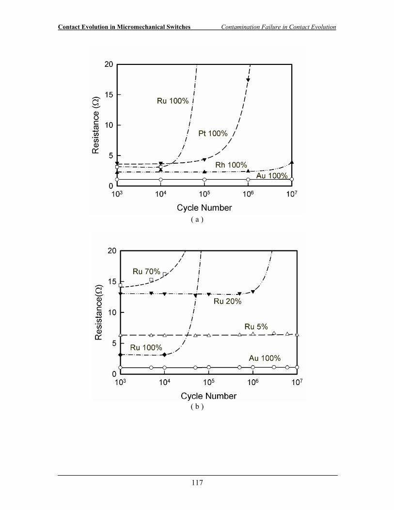
Contact Evolution in Micromechanical Switches Contamination Failure in Contact Evolution
117
( a )
( b )
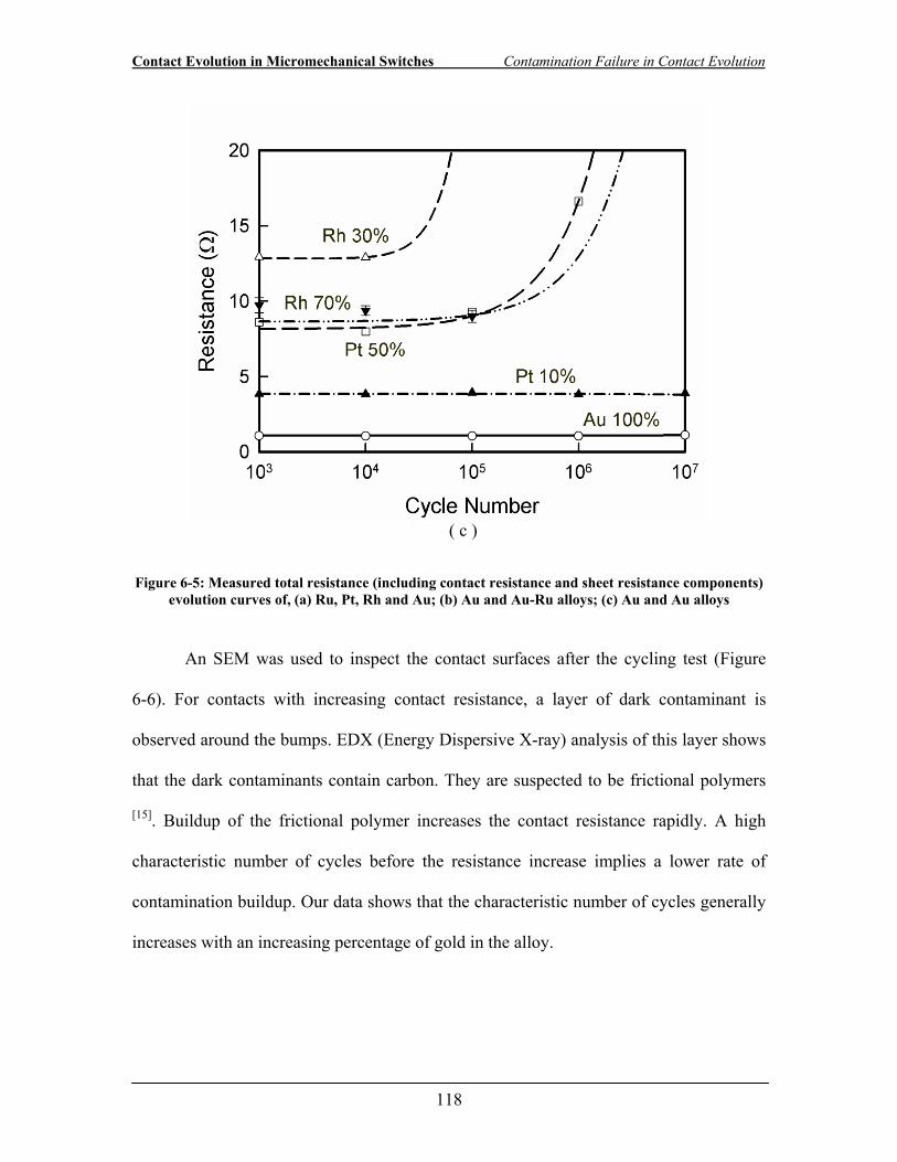
Contact Evolution in Micromechanical Switches Contamination Failure in Contact Evolution
118
( c )
Figure 6-5: Measured total resistance (including contact resistance and sheet resistance components) evolution curves of, (a) Ru, Pt, Rh and Au; (b) Au and Au-Ru alloys; (c) Au and Au alloys
An SEM was used to inspect the contact surfaces after the cycling test (Figure
6-6). For contacts with increasing contact resistance, a layer of dark contaminant is
observed around the bumps. EDX (Energy Dispersive X-ray) analysis of this layer shows
that the dark contaminants contain carbon. They are suspected to be frictional polymers
[15]. Buildup of the frictional polymer increases the contact resistance rapidly. A high
characteristic number of cycles before the resistance increase implies a lower rate of
contamination buildup. Our data shows that the characteristic number of cycles generally
increases with an increasing percentage of gold in the alloy.
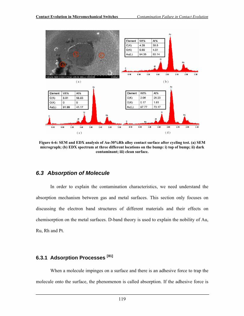
Contact Evolution in Micromechanical Switches Contamination Failure in Contact Evolution
119
Figure 6-6: SEM and EDX analysis of Au-30%Rh alloy contact surface after cycling test. (a) SEM micrograph; (b) EDX spectrum at three different locations on the bump: i) top of bump; ii) dark
contaminant; iii) clean surface.
6.3 Absorption of Molecule
In order to explain the contamination characteristics, we need understand the
absorption mechanism between gas and metal surfaces. This section only focuses on
discussing the electron band structures of different materials and their effects on
chemisorption on the metal surfaces. D-band theory is used to explain the nobility of Au,
Ru, Rh and Pt.
6.3.1 Adsorption Processes [81]
When a molecule impinges on a surface and there is an adhesive force to trap the
molecule onto the surface, the phenomenon is called absorption. If the adhesive force is
Contact Evolution in Micromechanical Switches Contamination Failure in Contact Evolution
120
weak and bonds between the molecule and surface are of the van der Waals type, the
adsorption is called physisorption. There is no electron exchange between the surface and
the molecule. The strength of bond is usually 0.25eV or less. However, if the adhesive
force between the molecule and surface is strong and bonds are covalent or ionic bonds,
the adsorption is called chemisorption. For chemisorption, electron orbital of molecule
and surface are overlapping. Valence electrons from the molecule and the valence
electrons from the metal mix with each other, which forms covalent bonding. In some
extreme cases, the electrons from the molecule move to the metal and form ionic
bonding. The binding energy of chemisorption is high, from 0.43eV for nitrogen on
nickel to about 8.4eV for oxygen on tungsten.
6.3.2 Newns-Anderson Model [81]
A strong bond can form between the metal surface and molecule due to
chemisorption. The strength of the bond is related to the electron band structure on the
surface. The physical concept of chemisorption can be described by using Newns-
Anderson model. As shown in Figure 6-7, there are two extreme cases in interactions
between a metal surface and a molecule. In case a, the band structure of metal surface is
flat, that is the energy density distribution of electrons is uniform over the all energy
levels. In case b, the band structure of the metal surface is narrow, that is the energy
density distribution of electrons is narrowly confined to one energy region. When
molecules come close to these two different band structures, the response of the energy
state in the molecule is different. Here we consider a simple example, that the molecule
has a single electron state aε . When the molecule is absorbed on a surface with a uniform
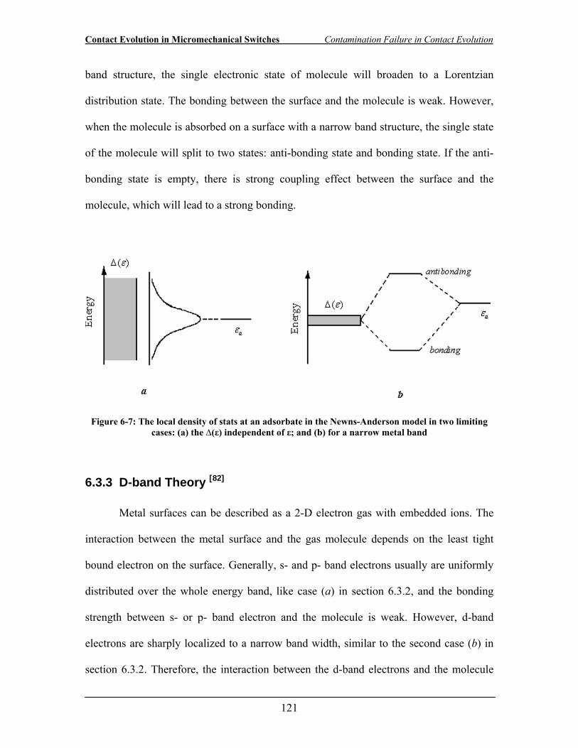
Contact Evolution in Micromechanical Switches Contamination Failure in Contact Evolution
121
band structure, the single electronic state of molecule will broaden to a Lorentzian
distribution state. The bonding between the surface and the molecule is weak. However,
when the molecule is absorbed on a surface with a narrow band structure, the single state
of the molecule will split to two states: anti-bonding state and bonding state. If the anti-
bonding state is empty, there is strong coupling effect between the surface and the
molecule, which will lead to a strong bonding.
Figure 6-7: The local density of stats at an adsorbate in the Newns-Anderson model in two limiting cases: (a) the ∆(ε) independent of ε; and (b) for a narrow metal band
6.3.3 D-band Theory [82]
Metal surfaces can be described as a 2-D electron gas with embedded ions. The
interaction between the metal surface and the gas molecule depends on the least tight
bound electron on the surface. Generally, s- and p- band electrons usually are uniformly
distributed over the whole energy band, like case (a) in section 6.3.2, and the bonding
strength between s- or p- band electron and the molecule is weak. However, d-band
electrons are sharply localized to a narrow band width, similar to the second case (b) in
section 6.3.2. Therefore, the interaction between the d-band electrons and the molecule
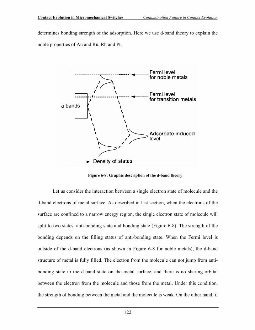
Contact Evolution in Micromechanical Switches Contamination Failure in Contact Evolution
122
determines bonding strength of the adsorption. Here we use d-band theory to explain the
noble properties of Au and Ru, Rh and Pt.
Figure 6-8: Graphic description of the d-band theory
Let us consider the interaction between a single electron state of molecule and the
d-band electrons of metal surface. As described in last section, when the electrons of the
surface are confined to a narrow energy region, the single electron state of molecule will
split to two states: anti-bonding state and bonding state (Figure 6-8). The strength of the
bonding depends on the filling status of anti-bonding state. When the Fermi level is
outside of the d-band electrons (as shown in Figure 6-8 for noble metals), the d-band
structure of metal is fully filled. The electron from the molecule can not jump from anti-
bonding state to the d-band state on the metal surface, and there is no sharing orbital
between the electron from the molecule and those from the metal. Under this condition,
the strength of bonding between the metal and the molecule is weak. On the other hand, if
Contact Evolution in Micromechanical Switches Contamination Failure in Contact Evolution
123
the metal has a partially filled d-band structure (as shown in Figure 6-8 for transition
metals), the anti-bonding state is empty. A covalent bond can be formed between the
metal and the molecule with the electrons from both sides sharing the same orbital. The
bonding strength is strong due to the covalent bonding.
Based on this analysis, it is clear that the strength of bonding is sensitive to the
position of the Fermi level relative to the d-band structure. For noble metals, such as
gold, the Fermi level is higher than the upper edge of the d-band electrons. The gold
surfaces have a fully filled d-band structure. With no empty anti-bonding states on the
surfaces, the bonding strength between adsorbed molecule and noble metals is weak.
However, for transition metals, such as Ru, Rh and Pt, the Fermi level is located inside of
the d-band structure. The transition metal surfaces have partially filled d-band structure.
With empty anti-bonding states, strong covalent bonds can form between the absorbed
molecule and the metals. It is very easy for these transition metals to adsorb molecules
from the air.
Hammer and Norskov [83] (1995) proposed a reactivity concept based on the
relative position of the d-band structure and Fermi level. They evaluate the surface
reactivity by comparing the relative distance between the center of d-band and the Fermi
level. The Fermi energy level is usually beyond the center energy of d-band electrons.
The farther the distance between the d-band center and the Fermi lever is, the nobler the
metal. The shift of the d-band center can change the reactivity of the surface. According
to d-band center theory, Greeley and Norsov [84] (2005) calculate the d-band center shift
due to the alloying effect. From their calculation, one atomic layer of the Ru, Rh and Pt
Contact Evolution in Micromechanical Switches Contamination Failure in Contact Evolution
124
on gold surface can shift up the d-band center of gold by 1.76eV, 1.91eV and 2.37eV
respectively. The higher d-band center will lead to higher reactivity.
The different contamination rates for different metals and metal alloys could be
related to their electron structure on the surfaces. Ru, Rh and Pt have partially filled d-
band electron structure on the surface, which makes them likely to absorb molecules from
the air and build up contaminant films. On the other hand, a filled d-band electron
structure on the surface makes gold more inert to contamination. For metal alloys, the
electron structure depends on the content of alloy elements. Alloy elements can shift the
d-band electron structure at the metal surfaces. It is not clear exactly how alloy elements
change the electron structure of our test materials. However, we found that alloys with
high Au content usually show lower contamination rates than those alloys with low Au
content. This trend is clearly demonstrated in the Ru-Au alloy test (Figure 6-5 (b)). By
increasing the Au content in the alloy, the characteristic number of cycles with stable
resistance increases from 104 for Au-70%Ru, to 106 for Au-20%Ru, and finally to more
than 107 for the Au-5%Ru alloy. The contamination rate for Au-70%Ru is similar to that
of Ru, while the contamination rate for Au-5%Ru is much lower.
6.4 Competition of Failure Mechanism
In general, contact materials with low hardness are more susceptible to contact
wear. Mechanical changes to the contact surface may disrupt the contaminate film,
reducing the increase of contact resistance. In order to investigate the effect of the alloy
elements and their relation to wear rate and contamination rate, we also compare the
contact evolution properties of Au-5%Ru and Au-10%Ru. Both alloys are cycled for 106
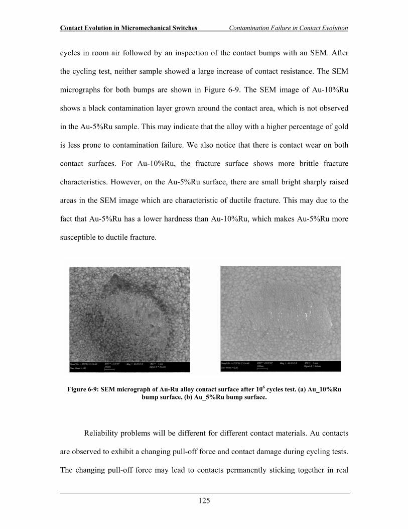
Contact Evolution in Micromechanical Switches Contamination Failure in Contact Evolution
125
cycles in room air followed by an inspection of the contact bumps with an SEM. After
the cycling test, neither sample showed a large increase of contact resistance. The SEM
micrographs for both bumps are shown in Figure 6-9. The SEM image of Au-10%Ru
shows a black contamination layer grown around the contact area, which is not observed
in the Au-5%Ru sample. This may indicate that the alloy with a higher percentage of gold
is less prone to contamination failure. We also notice that there is contact wear on both
contact surfaces. For Au-10%Ru, the fracture surface shows more brittle fracture
characteristics. However, on the Au-5%Ru surface, there are small bright sharply raised
areas in the SEM image which are characteristic of ductile fracture. This may due to the
fact that Au-5%Ru has a lower hardness than Au-10%Ru, which makes Au-5%Ru more
susceptible to ductile fracture.
Figure 6-9: SEM micrograph of Au-Ru alloy contact surface after 106 cycles test. (a) Au_10%Ru bump surface, (b) Au_5%Ru bump surface.
Reliability problems will be different for different contact materials. Au contacts
are observed to exhibit a changing pull-off force and contact damage during cycling tests.
The changing pull-off force may lead to contacts permanently sticking together in real
Contact Evolution in Micromechanical Switches Contamination Failure in Contact Evolution
126
switch operation. In our test, the pull-off force for gold contacts has been observed to
vary from 100µN to 200 µN during cycling tests. However, for materials with higher
hardness, the extent of contact wear and contact adhesion are greatly reduced. After
cycling tests, only minor contact wear has been observed in Au-5%Ru, Au-10%Ru, Au-
10%Pt and Rh, as compared with Au, with detected maximum pull-off force of 50µN,
50µN and 75µN and 50µN respectively. The reduction of the pull-off force in noble
metals and their alloys, compared to a gold contact, may due to the greater hardness
and/or greater surface reactivity. When materials are subjected to the same contact force,
the harder materials have smaller contact radii and smaller contact adhesion, which in
turn leads to a lesser pull-off force to separate. In addition, the growth of the frictional
polymer can further reduce the contact adhesion. After 105 contact cycles, the pull-off
force typically decreases to less than our detection threshold of 25 μN for all contact
materials tested with the exception of gold. Precautions such as surface deactivation
treatment [85], and hermetic packaging [4] for MEMS switches are known to be at least
partially effective in mitigating the effects of contamination. For many materials, contact
failure may depend on the competition between two failure mechanisms − contact wear
and contact contamination.
6.5 Conclusions
Thin films of Pt, Rh, Ru and their alloys with Au were deposited on silicon
substrates and investigated as electrical contact materials for RF MEMS switches. The
contact resistance was measured by a Scanning Probe Microscope test station and related
to measured values of material hardness and resistivity. The results show an increase in
Contact Evolution in Micromechanical Switches Contamination Failure in Contact Evolution
127
contact resistance and a decrease in hardness of Pt, Rh and Ru by alloying with Au, and
this increase/decrease was directly dependent upon the amount of Au. The overall trends
in electrical resistivity and contact resistance with alloying were similar.
The contact resistance includes constriction, sheet, and film resistances. The
initial contact resistance is greater than that predicted from the properties of the materials,
probably because of contaminant films. The contact resistance prediction is closer to the
experimental result for harder materials. This may indicate that contaminant films have
relatively less influence on contact resistance for hard materials, or that there are more
asperities in contact for those materials. However, surface films grow and greatly
increase the contact resistance during cyclic operation. Compared with Au, the noble
metals Ru, Rh and Pt are more susceptible to the growth of a contamination film. When
these metals are alloyed with Au, the alloying changes the contamination rate. High Au
content in an alloy can make the metal less susceptible to contamination failure. These
interrelationships among the contact resistance, hardness, and resistivity, along with the
methodology used in the present study, help to provide a basis for selection of optimum
electrical contact materials for RF MEMS switches.
Contact Evolution in Micromechanical Switches Conclusion and Future Work
128
7 Conclusion and Future Work
7.1 Conclusions
Contact evolution plays an important role in reliability issues of metal-contact
MEMS switches. During cyclic operation, changes of surface conditions and surface
morphology sometimes lead to large variations of contact resistance and pull off force.
These variations may cause the MEMS switches “fail to close” or “fail to open”. In order
to improve the reliability of MEMS switches, it is crucial to understand how contacts
evolve during the cycling test, and how this evolution might lead to switch failures. In
this work, a Scanning Probe Microscope (SPM) based contact tester was built to study
contact evolution. In particular, we investigated how contact evolution leads to changes
in adhesion and resistance in contacts for MEMS switches.
The change in adhesion was studied by using gold contacts. The magnitude of the
pull off force is related to the separation modes and separation dynamics. Two separation
modes, brittle and ductile, have been observed. By monitoring the force-displacement
separation curve and rate-dependent pull off force, we are able to identify the separation
mode during the contact test. These techniques are extremely useful for contact evolution
studies.
For brittle separation, the opening dynamics are controlled by events on the
surface. The magnitude of the pull off force in brittle mode depends on the bonding
strength between the interfaces. Longer time in contact results in larger pull off force.
The pull off force is larger at low cycling rates. Since all these tests were performed in
Contact Evolution in Micromechanical Switches Conclusion and Future Work
129
room air with humidity 30%~40%, the rate dependent pull off force may be related to the
kinetics of meniscus condensation.
For ductile separation, the opening dynamics are associated with the bulk
plasticity of the materials. During the separation, there are nano tips pulling out of the
surfaces. The elongation of these ductile tips leads to a plateau region in the force
displacement separation curve. Since the structures are pulled out at the nanometer scale,
surface tension driven diffusion causes viscous effects during separation. The time related
plastic elongation can cause larger pull off forces at a higher unloading rate. It was
observed that the pull off force at 300Hz can be 30~50µN larger than the pull off force at
0.5Hz during the ductile separation. In general, once the ductile separation has been
identified during the cycling test, the surface is found to be damaged, and the magnitude
of the pull off force shows very large scatter.
In this work, we compared the rate dependent pull off force at cycling rates of
300Hz and 0.5Hz. By measuring the difference between the two rate-dependent pull off
forces, for the first time, we demonstrate when and how the contact separates at every
stage of test.
We also evaluate effect of the size of the contact bump on contact adhesion. We
found that larger contact bumps will need larger pull off forces to separate. The
maximum detected pull off force seems to happen at a slow brittle separation. This could
be due to the meniscus force effects in brittle mode. When gold is used as the contact
material, ductile separation has been observed on all contact bump sizes.
We found that the best way to reduce ductile separation is to choose hard contact
materials. For example, by adding 5%Ru into Au, the hardness of the material is doubled.
Contact Evolution in Micromechanical Switches Conclusion and Future Work
130
The ductile fracture can be greatly reduced. Moreover, the pull off forces of Au-5%Ru
contacts are significant lower than those of the gold contacts. Note that by increasing the
Ru alloy content to 10%, contamination failure starts to occur.
We also surveyed different contact materials and their evolution performance.
According to our contact tests, we found two intrinsic material properties are critical to
the switch failures: one is the hardness, and the other is the electron structure on the metal
surfaces. It was found that a large amount of surface damage was only observed in gold
and gold alloys of low hardness. For instance, for gold contacts, ductile separation,
associated with a large amount of surface damage, is almost always seen. Minor surface
damage is also detected in contact materials with moderate hardness, such as Au-5%Ru,
Au-10%Ru and Au-10%Pt. However, for hard materials, such as Ru, Rh and Pt, large
amounts of surface damage are not observed in our experimental setup. On the other
hand, contamination failure is always seen in Ru, Rh and Pt contacts cycled in room air.
This may due to their partially filled d-band electron structure on their surface. During
cycling tests, a layer of frictional polymer could grow on these metal surfaces. This layer
of polymer can increase the contact resistance, and reduce the magnitude of the pull off
force.
For the metal alloys, the dominant failure mechanism is related to the content of
the alloy elements. It is found that, by increasing the content of the alloy elements (Ru,
Rh and Pt) in the gold thin film, both the hardness and the resistivity of the alloys
increases, as does the contamination rate. High gold content metal alloys are less prone
to the contamination failure, but are more prone to the ductile fracture. Such features
have been clearly demonstrated in the Ru-Au alloy contact tests.
Contact Evolution in Micromechanical Switches Conclusion and Future Work
131
7.2 Future work
According to our work, the SPM based contact tester has demonstrated strong
flexibility for contact studies. However, there are some limitations for using this contact
tester, such as sliding problems, and contamination problems. Future works could
improve the testing techniques, and investigate more details of contact physics.
To improve the testing techniques, different testing structures could be designed.
In this work, the testing structure used for contact tests is a free-end cantilever beam. This
testing structure has sliding problems during cycling tests. However, if we design some
new testing structures, such as beam bridges, the sliding problem could be removed. This
would help us design better experiments for contact study.
Another improvement of the testing technique could be introducing in-situ
cleaning processes for contact testing. Contact evolution is strongly affected by the
surface cleanness. Surface cleanness directly affects the separation mode, pull off force
and contact resistance. By keeping contact surfaces clean, we would expect different
evolution features from the tests in air. One possible way to obtain a clean testing
environment could be introducing a plasma source into the testing chamber. By cleaning
the contact surface with plasma treatment, we can study contact response without
contamination film.
For future contact study, time-related contact evolution could an interesting topic.
We have seen that the time-relate issues during the contact could change the magnitude
of the pull off force, or may affect contact evolution. It would be interesting to study the
effects of the time in contact, the loading rate, the unloading rate, as well as how these
rate effects correlated to the environments.
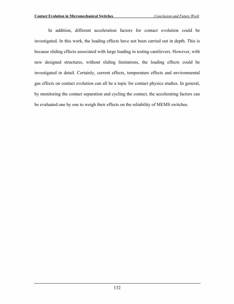
Contact Evolution in Micromechanical Switches Conclusion and Future Work
132
In addition, different acceleration factors for contact evolution could be
investigated. In this work, the loading effects have not been carried out in depth. This is
because sliding effects associated with large loading in testing cantilevers. However, with
new designed structures, without sliding limitations, the loading effects could be
investigated in detail. Certainly, current effects, temperature effects and environmental
gas effects on contact evolution can all be a topic for contact physics studies. In general,
by monitoring the contact separation and cycling the contact, the accelerating factors can
be evaluated one by one to weigh their effects on the reliability of MEMS switches.
Contact Evolution in Micromechanical Switches Appendix I
133
APPENDIX I: SANDWICH STRUCTURE FOR SLIDING
CANCELLATION
In order to cancel out the sliding in the X direction, a two wedge sandwich (Figure
7-1) structure was used for the contact test in combination with a small angle
approximation. In this design, wedge 2 is used to provide an actuation direction, while
the actuation direction was tilted at an angle ϕ relative to the direction Z. Then, Wedge
1 was used to keep the substrate parallel to the cantilever. Using this design, the lateral
movement of the bump was cancelled by the simultaneous movement of the substrate. If
we assume the contact stiffness is infinite, based on the dimension of our test cantilever,
the angle ϕ should be chosen as 7.5˚.
Figure 7-1: Contact angle set-up for cyclic test. Two wedges are used to cancel the sliding movement during the actuation. Wedge 2 is used to provide an actuation angle and wedge 1 is used to keep the
substrate parallel to the cantilever.
Contact Evolution in Micromechanical Switches Appendix I
134
The assumption of infinite contact stiffness can be made when a very compliant
cantilever is used. However, in the case of our stiff test cantilevers, the spring constant of
the cantilever was within an order of magnitude of the contact stiffness. Therefore, the
contact stiffness needed to be included in the compensation angle calculation. Herzian
elastic contact theory was used to estimate the contact stiffness. The contact was
modeled as an elastic contact between a half sphere and a flat plane. The curvature of the
contact sphere is R, and the loading force is P, with a contact radius a, the indentation
depth δ can be expressed as:
3/1
⎟⎠⎞
⎜⎝⎛ ⋅
=K
RPa (Equation 7-1)
3/1
2
22
⎟⎟⎠
⎞⎜⎜⎝
⎛⋅
==KR
PRaδ (Equation 7-2)
In these equations, K is the effective Young’s modulus and it is a combination of the
Young’s modulus of the two contact materials (E1 and E2) as well as Poisson ratios (ν1,
ν2):
)11(431
2
22
1
21
EEKνν −
+−
⋅= (Equation 7-3)
The contact stiffness ck can be calculated by dividing the force by the depth δ:
Contact Evolution in Micromechanical Switches Appendix I
135
3/13/12 )( PKRPkc ⋅⋅==δ
(Equation 7-4)
This equation shows that the contact stiffness is related to the force as well as the
hemisphere’s radius. As an example, let us assume the contact is between gold thin films.
In this case the Young’s modulus is E1=E2=91GPa, and the Poisson ratio is ν1=ν2=0.32.
Given a contact bump with the radius of curvature of 20μm at an applied contact force of
200μN, the contact stiffness is 4105.1 × N/m. This value of the contact stiffness is of the
same magnitude as the stiffness of our test cantilevers ( 44 100.2~108.0 ×× N/m). Thus, if
we want to calculate the compensation angle, the contact stiffness should be considered.
In the condition of having a finite contact stiffness, there is an indentation depth δ
between the contacts. Consider subZΔ as the substrate movement in the Z direction. For
contact with finite stiffness, subZΔ should be in terms of the cantilever movement ∆Z and
the contact indentation depth δ:
δ+Δ=Δ ZZ sub (Equation 7-5)
The horizontal movement in the X direction due to the deflection of the cantilever can be
re-written as:
)(23)
23( δ−Δ⋅
⋅⋅
=Δ⋅⋅⋅
=Δ subZLhZ
LhX (Equation 7-6)
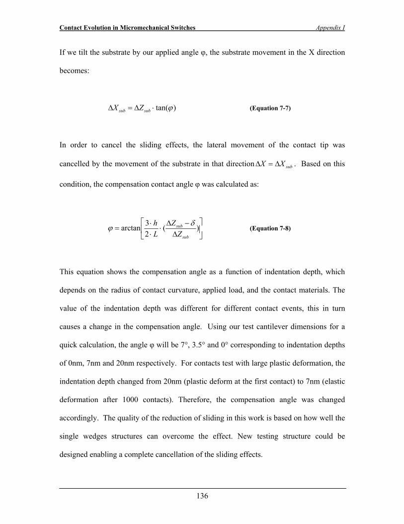
Contact Evolution in Micromechanical Switches Appendix I
136
If we tilt the substrate by our applied angle φ, the substrate movement in the X direction
becomes:
)tan(ϕ⋅Δ=Δ subsub ZX (Equation 7-7)
In order to cancel the sliding effects, the lateral movement of the contact tip was
cancelled by the movement of the substrate in that direction subXX Δ=Δ . Based on this
condition, the compensation contact angle φ was calculated as:
⎥⎦
⎤⎢⎣
⎡Δ
−Δ⋅
⋅⋅
= )(23arctan
sub
sub
ZZ
Lh δϕ (Equation 7-8)
This equation shows the compensation angle as a function of indentation depth, which
depends on the radius of contact curvature, applied load, and the contact materials. The
value of the indentation depth was different for different contact events, this in turn
causes a change in the compensation angle. Using our test cantilever dimensions for a
quick calculation, the angle φ will be 7°, 3.5° and 0° corresponding to indentation depths
of 0nm, 7nm and 20nm respectively. For contacts test with large plastic deformation, the
indentation depth changed from 20nm (plastic deform at the first contact) to 7nm (elastic
deformation after 1000 contacts). Therefore, the compensation angle was changed
accordingly. The quality of the reduction of sliding in this work is based on how well the
single wedges structures can overcome the effect. New testing structure could be
designed enabling a complete cancellation of the sliding effects.
Contact Evolution in Micromechanical Switches Appendix II
137
APPENDIX II: PREPARATION FOR CYCLING TEST
The procedure for the contact test is as following:
1. Contact material is firstly deposited on both testing cantilever and planar
substrate. If the contact surfaces are coated with a protection layer of TiW, the
TiW layer should be stripped using hydrogen peroxide right before the test.
2. The cantilever is directly attached to cantilever holder in the SPM system. The
planar substrate needs to be assembled with a piezoelectric actuator (PL022) and a
12° wedge. The three parts are glued together using Thermoplastic (STAYSIK®
Thermoplastic Adhesive 442). The assembling is performed on a hotplate which
is heated up to 115°C. Once the planar substrate, piezoelectric actuator and the
contact wedge are stably attached to each other, the structure is cooled down and
put into the SPM stage.
3. When nitrogen is used for the test, a micrometer stage is used to move gas tube
close to the substrate. The gas flow rate is controlled at 500 sccm.
4. Apply a DC bias voltage to the piezoelectric actuator (30V). Using the SPM
control program (“Contact Mode”) to move the substrate to the test position.
(Note that deflection of the cantilever can be readout by the output voltage from
photo detector. If we set -2.0V as free standing position of the cantilever tip, -
1.9V is usually used as set point value for stage approach). Follow the procedure
in the JSPM-5200 manual to perform the laser alignment and approaching
procedure. If the planar substrate is not parallel to the subside face of the
Contact Evolution in Micromechanical Switches Appendix II
138
cantilever, the laser spot movement may not be vertical. It is important to adjust
the angle of the wedge to cancel the twist. The angle adjustment and reloading
check may need to be done several times to get the right contact angle.
5. Once the twist is cancelled, the sample is ready for contact test. Turn off the
feedback control for SPM stage, when the planar substrate is in the set position (-
1.9V). (In JSPM, this function can be realized by disabling the feedback). Then
manually decrease the biased the voltage for piezoelectric actuator to 15V, which
will move the planar substrate away from the cantilever bump.
6. Apply an AC voltage/or programmed signal to the piezoelectric actuator, and turn
on the data acquisition program in LabVIEW as well. Choose the AC output
amplitude as 1Vp-p, and then adjust DC biased, make sure the maximum contact
force reaches to a desired value. For cycling test, keep the contact cycling rate and
the maximum contact force constant and record the force data.
7. If contact resistance is included in the measurement, a four-wire probe is needed
to be assembled on the surfaces as well. For gold contact, the solder can be used
to connect the two probes to the planar substrate. However, for the transition
metals, such as Ru and Rh, the silver paint is used. The probing leads are first
glued to the substrate by using conductive film (STAYSTIK 541) on the hotplate
with temperature of 115°C. The silver paint is then applied afterwards to improve
the conductivity. On the cantilever holder side, the silver paint is also used to for
metal contacts.
Contact Evolution in Micromechanical Switches Appendix III
139
APPENDIX III: FABRICATION OF ROUND BUMP WITH DIFFERENT
RADII
The radii of fabricated contact bumps are related to the reflowed curvature of
photoresist(PR). Since the base diameter of PR is barely moved during the reflow, the
curvature of the reflowed PR is limited by the surface tension, the thickness of PR and
based diameter of PR. In this work, I choose four different size PR pattern for round
bump fabrication. The diameter for the PR patterns is chosen as 3μm, 5μm, 8μm and
13μm. Shieply 1813 is used to prepare the PR bump. The shape of the silicon after
etching is shown in the following. The radius of the curvature of silicon bumps after
fabrication is 4 μm, 15 μm, 22 μm and 40μm respectively.
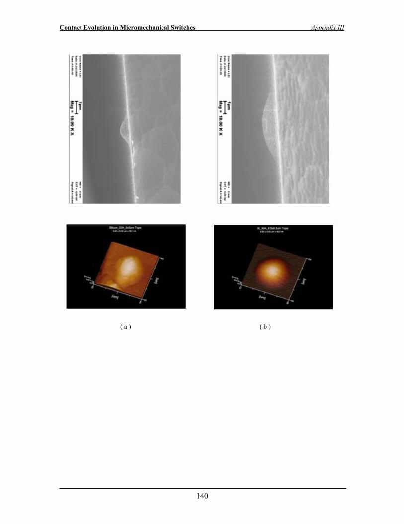
Contact Evolution in Micromechanical Switches Appendix III
140
( a ) ( b )
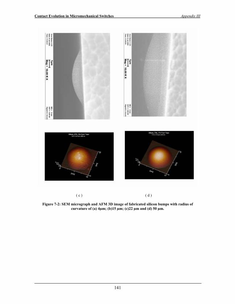
Contact Evolution in Micromechanical Switches Appendix III
141
( c ) ( d )
Figure 7-2: SEM micrograph and AFM 3D image of fabricated silicon bumps with radius of curvature of (a) 4µm; (b)15 µm; (c)22 µm and (d) 50 µm.
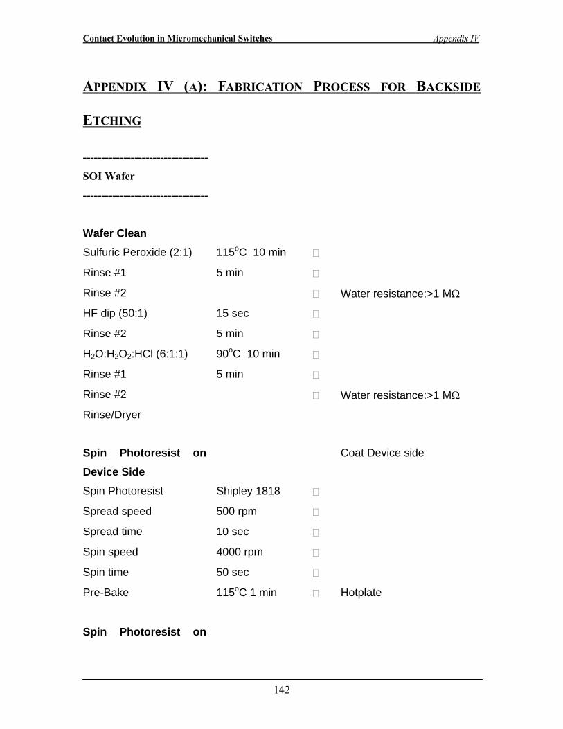
Contact Evolution in Micromechanical Switches Appendix IV
142
APPENDIX IV (A): FABRICATION PROCESS FOR BACKSIDE
ETCHING
----------------------------------
SOI Wafer
----------------------------------
Wafer Clean
Sulfuric Peroxide (2:1) 115oC 10 min
Rinse #1 5 min
Rinse #2 Water resistance:>1 MΩ
HF dip (50:1) 15 sec
Rinse #2 5 min
H2O:H2O2:HCl (6:1:1) 90oC 10 min
Rinse #1 5 min
Rinse #2 Water resistance:>1 MΩ
Rinse/Dryer
Spin Photoresist on Device Side
Coat Device side
Spin Photoresist Shipley 1818
Spread speed 500 rpm
Spread time 10 sec
Spin speed 4000 rpm
Spin time 50 sec
Pre-Bake 115oC 1 min Hotplate
Spin Photoresist on
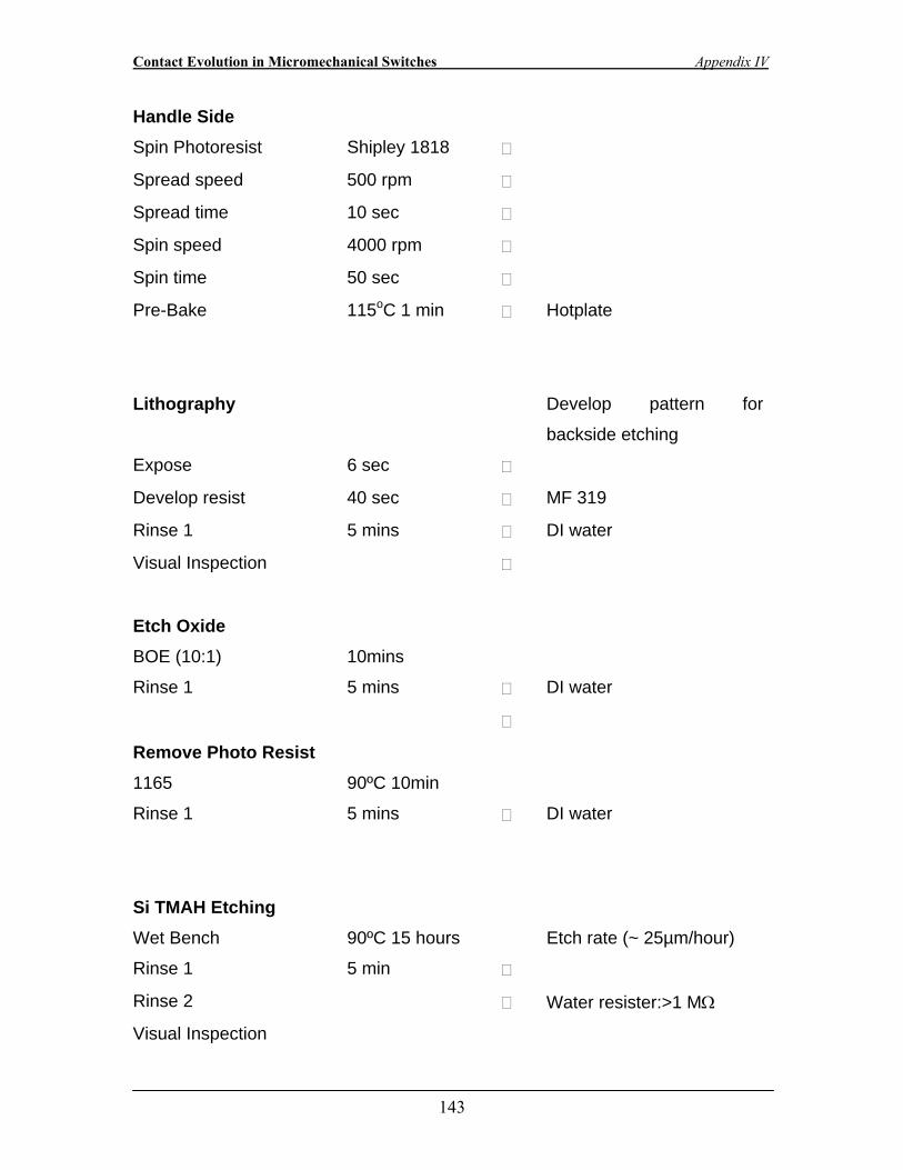
Contact Evolution in Micromechanical Switches Appendix IV
143
Handle Side Spin Photoresist Shipley 1818
Spread speed 500 rpm
Spread time 10 sec
Spin speed 4000 rpm
Spin time 50 sec
Pre-Bake 115oC 1 min Hotplate
Lithography Develop pattern for
backside etching
Expose 6 sec
Develop resist 40 sec MF 319
Rinse 1 5 mins DI water
Visual Inspection
Etch Oxide
BOE (10:1) 10mins
Rinse 1 5 mins DI water
Remove Photo Resist
1165 90ºC 10min
Rinse 1 5 mins DI water
Si TMAH Etching
Wet Bench 90ºC 15 hours Etch rate (~ 25µm/hour)
Rinse 1 5 min
Rinse 2 Water resister:>1 MΩ
Visual Inspection

Contact Evolution in Micromechanical Switches Appendix IV
144
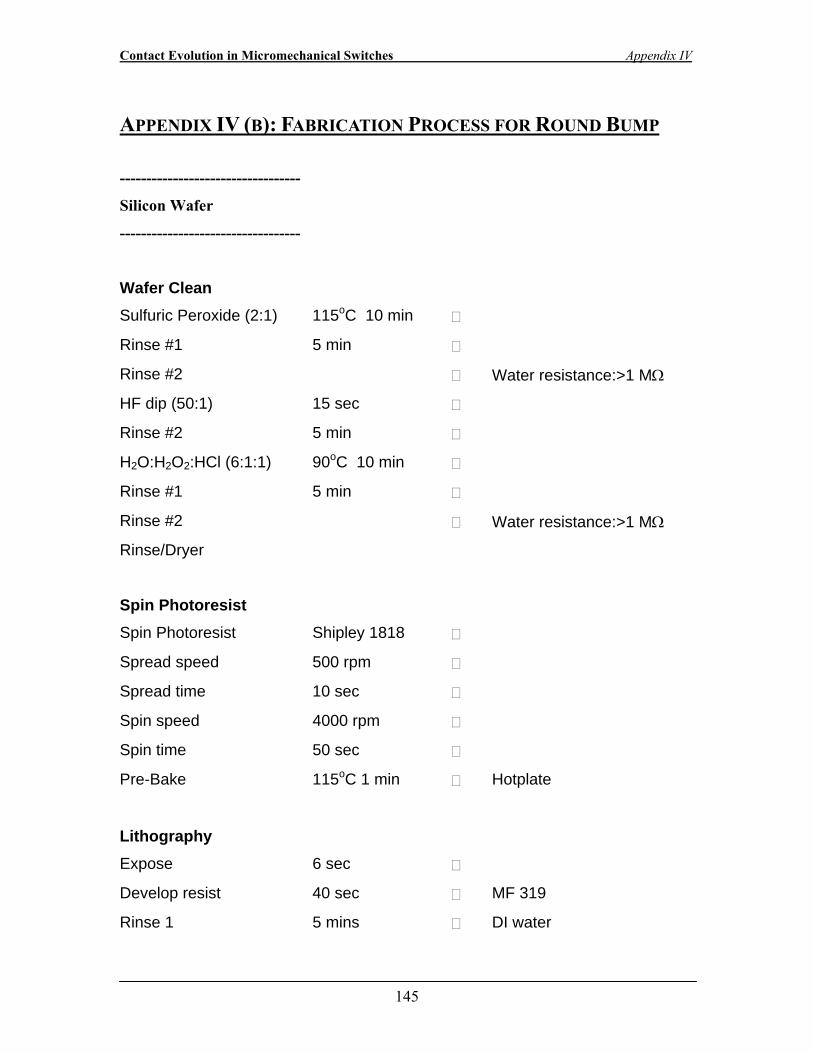
Contact Evolution in Micromechanical Switches Appendix IV
145
APPENDIX IV (B): FABRICATION PROCESS FOR ROUND BUMP
----------------------------------
Silicon Wafer
----------------------------------
Wafer Clean
Sulfuric Peroxide (2:1) 115oC 10 min
Rinse #1 5 min
Rinse #2 Water resistance:>1 MΩ
HF dip (50:1) 15 sec
Rinse #2 5 min
H2O:H2O2:HCl (6:1:1) 90oC 10 min
Rinse #1 5 min
Rinse #2 Water resistance:>1 MΩ
Rinse/Dryer
Spin Photoresist
Spin Photoresist Shipley 1818
Spread speed 500 rpm
Spread time 10 sec
Spin speed 4000 rpm
Spin time 50 sec
Pre-Bake 115oC 1 min Hotplate
Lithography
Expose 6 sec
Develop resist 40 sec MF 319
Rinse 1 5 mins DI water
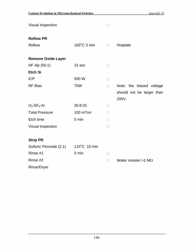
Contact Evolution in Micromechanical Switches Appendix IV
146
Visual Inspection
Reflow PR
Reflow 165oC 3 min Hotplate
Remove Oxide Layer
HF dip (50:1) 15 sec
Etch Si
ICP 500 W
RF Bias 70W Note: the biased voltage
should not be larger than
200V.
O2:SF6:Ar 35:8:25
Total Pressure 100 mTorr
Etch time 5 min
Visual Inspection
Strip PR
Sulfuric Peroxide (2:1) 115oC 10 min
Rinse #1 5 min
Rinse #2 Water resister:>1 MΩ
Rinse/Dryer
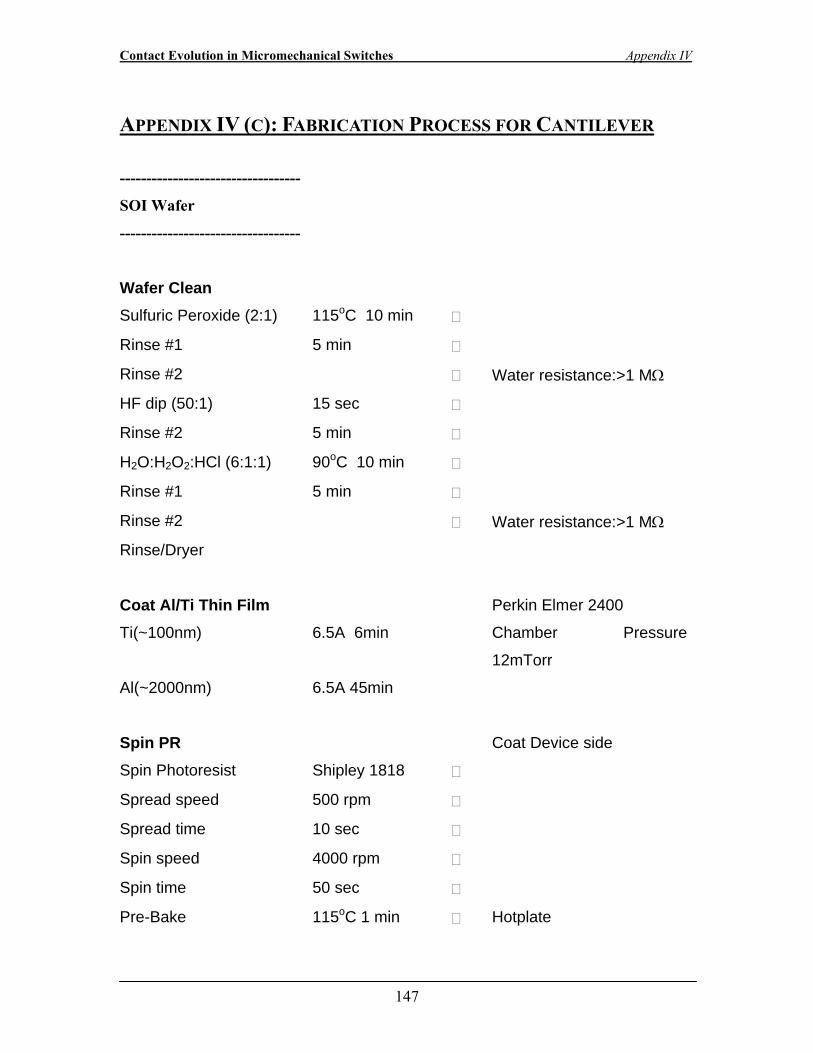
Contact Evolution in Micromechanical Switches Appendix IV
147
APPENDIX IV (C): FABRICATION PROCESS FOR CANTILEVER
----------------------------------
SOI Wafer
----------------------------------
Wafer Clean
Sulfuric Peroxide (2:1) 115oC 10 min
Rinse #1 5 min
Rinse #2 Water resistance:>1 MΩ
HF dip (50:1) 15 sec
Rinse #2 5 min
H2O:H2O2:HCl (6:1:1) 90oC 10 min
Rinse #1 5 min
Rinse #2 Water resistance:>1 MΩ
Rinse/Dryer
Coat Al/Ti Thin Film Perkin Elmer 2400
Ti(~100nm) 6.5A 6min Chamber Pressure
12mTorr
Al(~2000nm) 6.5A 45min
Spin PR Coat Device side
Spin Photoresist Shipley 1818
Spread speed 500 rpm
Spread time 10 sec
Spin speed 4000 rpm
Spin time 50 sec
Pre-Bake 115oC 1 min Hotplate
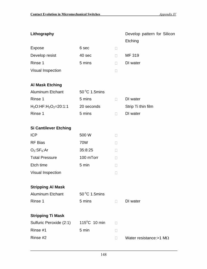
Contact Evolution in Micromechanical Switches Appendix IV
148
Lithography Develop pattern for Silicon
Etching
Expose 6 sec
Develop resist 40 sec MF 319
Rinse 1 5 mins DI water
Visual Inspection
Al Mask Etching
Aluminum Etchant 50 oC 1.5mins
Rinse 1 5 mins DI water
H2O:HF:H2O2=20:1:1 20 seconds Strip Ti thin film
Rinse 1 5 mins DI water
Si Cantilever Etching
ICP 500 W
RF Bias 70W
O2:SF6:Ar 35:8:25
Total Pressure 100 mTorr
Etch time 5 min
Visual Inspection
Stripping Al Mask
Aluminum Etchant 50 oC 1.5mins
Rinse 1 5 mins DI water
Stripping Ti Mask
Sulfuric Peroxide (2:1) 115oC 10 min
Rinse #1 5 min
Rinse #2 Water resistance:>1 MΩ
Contact Evolution in Micromechanical Switches Appendix IV
149
Remove Oxide Layer
BOE (10:1) 10mins
Rinse 1 5 mins DI water
Contact Evolution in Micromechanical Switches References
150
References
1. K. Petersen, “Micromechanical Membrane Switches on Silicon”, IBM Journal of Research and
Development, 23, 376-385, 1979
2 . C.L. Goldsmith, J. Randall, S. Eshelman, T.H. Lin, D. Denniston, S. Chen, and B. Norvell,
“Characteritics of Micromachined Switches at Microwave Frequencies”, IEEE International Microwave
Symposium Digest, 1141-1144, 1996
3. G.M. Rebeiz, J.B. Muldavin, “RF MEMS Switches and Switch Circuits”, IEEE Microwave Magazine,
12, 59-71, 2001
4. S. Majumder, J. Lampen, R. Morrison, “MEMS Switches”, IEEE Instrumentation & Measurement
Magazine, 6, 12-15, 2003
5. D. Maugis, Contact, Adhesion and Rupture of Elastic Solids, Springer, 2000
6. J.W. Tringe and T.A.Uhlman, “A Single Asperity Study of Au/Au Electrical Contacts”, Journal of
Applied Physics, 93,8, 46614669, 2003
7. R. Holm, Electric Contacts, 4th ed., Berlin, Germany:Springer-Verlag, 1967
8 . T. H. Courtney, Mechanical Behavior of Materials, McGraw-Hill Publishing Company, 1990
9. K.B. Lee, S.M. Lee and J. Cheon, “Size-Controlled Synthesis of Pd Nanowires Using a Mesoporous
Silica Template via Chemical Vapor Infiltration”, Advanced Materials, 13, 517-520, 2001
Contact Evolution in Micromechanical Switches References
151
10. S.T. Patton and J.S. Zabinski, “Fundamental Studies of Au Contacts in MEMS RF Switches”,
Tribology Letters, 18, No. 2, 215-230, 2005
11. A. Gill, J. Colchero “Different Stage of Water Adsorption on Au Studies by Dynamic of SFM and
Jumping Mode”, Applied Physics A, 72, S137-S140, 2001
12. D. Hyman and M. Mehregany, “Contact Physics of Gold Microcontacts for MEMS Switches”, IEEE
Transactions on Components and Packaging Technology, 22, No.3, 357-364, 1999
13. B.D. Jensen, L.L.W. Chow, K.W. Huang, K. Saitou, J.L. Volakis, K. Kurabayashi “Effect of
Nanoscale Heating on electrical Transport in RF MEMS Switch Contacts”. Journal of
Microelectromechanical System, 14, 935~946, 2005
14. J. Schimkat, “Contact Measurements Providing Basic Design Data for Microrelay”, Sensors and
Actuators, 73, 138-143, 1999
15. M. Antler, “Survey of Contact Fretting in Electrical Connectors” IEEE Transactions on Components ,
Hybrids, and Manufacturing Technology, CHMT-8, 87-104, 1985
16. L.H. Germer, “Physical Processes in Contact Erosion”, Journal of Applied Physics, 29, 1067-1083,
1958.
17. S. Majumder, “Contact Properties of A Microelectromechanical Switch with Gold-on-Gold Contacts ”,
Ph.D. Thesis, ECE Department, Northeastern University, 2003
18. B.D. Jensen, K.W. Huang, L.L.-W. Chow and K. Kurabayashi, “Adhesion Effects on Contact Opening
Dynamics in Micromechined Switches”, Journal of Applied Physics, 97, 103535, 2005
Contact Evolution in Micromechanical Switches References
152
19. R. Chan, R. Lesnick, D. Becher, and M. Feng, “Low-Actuation Voltage RF MEMS Shunt Switch With
Cold Switching Lifetime of Seven Billion Cycles”, Journal of Microelectromechanical System, 12, 713-719,
2003
20. D.J. Dickrell and M.T. Dugger, “The Degradation of Electrical Contact Resistance of Metal Films at
Low Contact Force”, Proceedings of 2004 ASME/STLE International Joint Tribology Conference, Long
Beach, California USA, TRIB2004-64332, 2004
21. A. Lumbantobing, L. Kogut, and K. Komvopoulos, “Electrical Contact Resistance as a Diagnostic
Tool for MEMS Contact Interfaces”, Journal of Microelectromechanical Systems, 13, 977-987,2004
22. G. Gregori, R.E. Mihailiovich, J.F. DeNatale and D.R. Clarke, “Development of Adhesive Contact of
MEMS-Swtiches Upon Actuation Cycling”, 18th IEEE International Conference on Micro Electro
Mechanical Systems, 439-442, 2005
23. G. Gregori and D.R. Clarke, “Mechanical Creep as a Life-limiting Factor of Radio Frequency
Microswitches”, Applied Physics Letters, 87, 154101-3, 2005
24. R.A. Coutu, Jr.P.E. Kladitis, K.D. Leedy and R.L. Crane, “Selecting Metal Alloy Electrical Contact
Materials for MEMS Switches”, Journal of Micromechancis and Microengineering, 14, 1157-1164, 2004
25. E.L. Cussler, Diffusion: Mass Transfer in Fluid System, Second Edition, Cambridge University Press,
pp. 53, 1997.
26 . E.L. Cussler, Diffusion: Mass Transfer in Fluid System, Second Edition, Cambridge University Press,
pp. 103, 1997.
Contact Evolution in Micromechanical Switches References
153
27. D. Maugis, Contact, Adhesion and Rupture of Elastic Solids, Springer, 2000
28. K.L. Johnson, K. Kendall, and A.D.Roberts, “Surface Energy and The contact of Electric Solids”,
Proceedings of the Royal Society A, 324, 301-313, 1971
29. B.V. Deriaguin, V.M. Muller, and Y.P. Toporov, “Effect of Contact Deformations on the Adhesion of
Particles”, Journal of Colloidal Interface Science, 53, 314-326, 1975
30. D. Tabor, “ Surface Forces and Surface Interactions”, Journal of Colloid and Interface Science, 58, 2-
13, 1977
31. D. Maugis, “The JKR-DMT Transition Using a Dugdale Model”, Journal of Colloid and Interface
Science, 150, 243-269, 1992
32. J.A. Greenwood, “Adhesion of Elastic Sphere”, Proceedings of the Royal Society A, 453, 1277-1297,
1997
33. Y. Du, L. Chen, N.E. McGruer, G.G. Adams, I. Etsion, “ A Finite Element Model of Loading and
Unloading of an Asperity Contact with Adhesion and Plasticity”, Journal of Colloid and Interface Science,
312, 522-528, 2007.
34. P.R. Cha, D.J. Srolovitz, “Molecular Dynamics Simulation of Single Asperity Contact”, Acta
Materialia, 52, 3983-3996, 2004
35. J. Song, D.J. Srolovitz, “Adhesion Effects in Material Transfer in Mechanical Contacts”, Acta
Materialia, 54, 5305-5312, 2006
36. F.P. Bowden and D. Tabor, Friction and Lubrication of Solids, Vol.1, 1951
Contact Evolution in Micromechanical Switches References
154
37. P.E. Marszalek, W.J. Greenleaf, H.Li, A.F. Oberhauser, J.M.Fernandez, “Atomic Force Microcopy
Captures Quantized Plastic Deformation in Gold Nanowires.” Proceedings of the National Academy of
Sciences, 97, 6282-6286, 2000
38. H.M. Pollock, P. Shufflebottom and J. Skinner, “ Contact Adhesion between Solids in Vacuum: I.
Single-asperity Experiments”, Journal of Physics, D: Applied Physics, 10, 127-138, 1977
39. D. Maugis and M. Barquins, “Fracture Mechanics and the Adherence of Viscoelastic Bodies”, Journal
of Physics D: Applied Physics, 11, 1989-2023, 1978
40. A.A. Griffith, “The Phenomena of Rupture and Flow in Solids”, Philosophical Transactions of The
Royal Society, London, A221, 163, 1920
41. G. R. Irwin , “Analysis of Stress and Strains Near the End of A Crack Traversing a Plate”, Journal of
Applied Mechanics, 24, 361-364, 1957
42. E. Orowan, “Fundamental of Brittle Behavior in Metals”, Fatigue and Fracture of Metals, 139-167,
1952
43. Y.G. Wei, J.W. Hutchinson, “ Models of Interface Separation Accompanied by Plastic Dissipation at
Multiple Scales”, International Journal of Fracture, 95, 1-17, 1999
44. J.W. Kysar, “Energy Dissipation Mechanisms in Ductile Fracture”, Journal of the Mechanics and
Physics of Solids, 51, 795-824, 2003
45 . J.R. Rice and R. Thomson, “Ductile Versus Brittle Behavior of Crystals”, Philosophical Magzine, 29,
73-97, 1974
Contact Evolution in Micromechanical Switches References
155
46. J.R. Rice, “Dislocation Nucleation From a Crack Tip: An Analysis Based on the Peierls Concept”,
Journal of the Mechanics and Physics of Solids, 40, 239-271, 1992
47. G.E. Beltz, D.M. Lipkin, and L.L. Fischer, “Role of Crack Blunting in Ductile Versus Brittle Response
of Crystalline Materials”, Physical Review Letter, 82 (22), 4468-4471, 1999
48. H.B. Zeng, N. Maeda, N.H. Chen, M. Tirrell and J. Israelachvili, “ Adhesion and Friction of
Polystyrene Surfaces around Tg”, Macromolecules, 39(6), 2350-2363, 2006.
49. E. Riedo, F. Levy, H. Brune, “Kinetics of Capillary Condensation in Nanoscopic Sliding Friction”,
Physical Review Letter, 88, 185505, 2002
50. I. Etsion, Y. Kligerman, Y. Kadin, “Unloading of an Elastic-Plastic Loaded Spherical Contact”,
International Journal of Solids and Structures, 42, 3716-3729, 2005
51. L. Kogut and I. Etsion, “Adhesion in Elastic-Plastic Spherical Microcontact”, Journal of Colloid and
Interface Science, 261, 372-378, 2003.
52. A. Gil, J. Colchero, J. Gómez-Herrero, A.M. Baró, “Different Stages of Water Adsorption on Au
Studied by Dynamic SFM and Jumping Mode”, Applied Physics A, 72, S137-S140, 2001
53. B. Bhushan, Tribology and Mechanics of Magnetic Storage Devices, 2nd ed., Springer, New York, 1996
54. R. Szoszkiewicz and E. Riedo, “ Nucleation Time of Nanoscale Water Bridges”, Physical Review
Letter, 95, 135502, 2005
Contact Evolution in Micromechanical Switches References
156
55. M.M. Wu, T. Cubaud, and C.M. Ho, “Scaling Law in Liquid Drop Coalescence Driven by Surface
Tension”, Physics of Fluids, 16, L51-L54, 2004
56. T. H. Courtney, Mechanical Behavior of Materials, McGraw-Hill Publishing Company, 1990
57. J.L. Wang, X.S. Chen, G.H. Wang, B.L. Wang, W. Lu and J.J. Zhao, “ Melting Behavior in Ultrathin
Metallic Nanowires”, Physical Review B, 66, 085408, 2002
58. K.B. Lee, S.M. Lee and J. Cheon, “Size-Controlled Synthesis of Pd Nanowires Using a Mesoporous
Silica Template via Chemical Vapor Infiltration”, Advanced Materials, 13, 517-520, 2001
59. J.H. Kim, D.J. Srolovitz, P.R. Cha, J.K. Yoon, “Capillarity and electromigration Effects on Asperity
Contact Evolution in Microelectromechanical System Switches” Journal of Applied Physics, 100, 054502-
8, 2006
60. N. Agraїt, A.L. Yeyati, and J. M. van Ruitenbeek, “Quantum Properties of Atomic-Sizes Conductors”
Physics Reports, 377, 81-279, 2003
61. M.R. Sørensen, M. Brandbyge and K.W. Jacobsen, “Mechanical deformation of atomic-scale metallic
contacts: structure and mechanisms”. Physics Review B, 57, 3283–3294, 1998
62. L. Kuipers and J.W.M. Frenken, “ Jump to Contact, Neck formation , and Surface melting in the
Scanning Tunneling Microscope”, Physics Review letters, 70, 3907-3910, 1993
63. T. Kizuka, “ Atomic Process of Point Contat in Gold Studied by Time-Resolved High-Resolution
Transmission Electron Mciroscopy”, Physical Review Letters, 81, 4448-4451, 1998
Contact Evolution in Micromechanical Switches References
157
64. N.A. Alcantar, C. Park, J. M. Pan, J. N. Israelachvili, “ Adhesion and Coalescence of Ductile Metal
Surfaces and Nanoparticles”, Acta Materialia, 51, 31-47, 2003
65. S. Arcidiacono, N.R. Bieri, D. Poulikakos, C.P. Grigoropoulos, “ On the Coalescence of Gold
Nanoparticles”, International Journal of Multiphase Flow, 30, 979-994, 2004
66. K.K. Nanda, S.N. Sahu, S.N. Behra, “ Liquid-drop Model for the Size-Dependent Melting of Low-
Dimensional Systems”, Physical Review A 66, 013208, 2002
67. A. H. Cottrell, The Mechanical Properties of Matter, Chapter 7, pp. 227, 1964
68. B. Bhushan, Introduction to Tribology, 2002
69. B. Bhushan, “ Adhesion and Stiction: Mechanisms, Measurement Techniques and Methods for
Reduction”, Journal of Vacuum Science and Technology B, 21, 2262-2296, 2003
70. D. Maugis, Contact, Adhesion and Rupture of Elastic Solids, Chapter 4, pp 314, 2000
71. J.S. McFarlane and D. Tabor, “Adhesion of Solids and the Effects of Surface Films”, Proceedings of the
Royal Society of London. Series A, 202, 224-243, 1950
72. M.J. Matthewson, “Adhesion of Spheres by Thin Liquid Films”, Philosophical Magazine A, 57, 207-
216, 1988.
73. R. Schweinfest, A.T. Oaxton and M.W. Finnis, “Bismuth Embrittlement of Copper is an Atomic Size
Effect”, Nature, 432, 1008-1011, 2004
Contact Evolution in Micromechanical Switches References
158
74. X.G. Liu, X.W. Wang, J.Y. Wang and H.Y. Zhang, “First Principles Investigation of Mg Segregation
at Σ=11(113) Grain Boundaries in Al”, Journal of Physics: Condensed Matter, 17, 4301-4308, 2005
75. R. Holm, Electric Contact, 4th ed., Berlin, Germany:Springer-Verlag, pp 4, 1967
76. R. Holm, Electric Contact, 4th ed., Berlin, Germany:Springer-Verlag, pp 124, 1967
77. H. Lee, R. A. Coutu, Jr, S. Mall, and K. D. Leedy, “Characterization of Metal and Metal Alloy Films
as Contact Materials In MEMS Switches”, Journal of Micromechanics and Microengineering, 16, 557-563,
2006
78. W. C. Oliver and G. M. Pharr, “ Review: Measurement of Hardness and Elastic Modulus by
Instrumented Indentation: Advances in Understanding and Refinements to Methodology”, Journal of
Materials Research, 19, 3-20, 2004
79. R. Holm, Electric Contact, 4th ed., Berlin, Germany: Springer-Verlag, pp125, 1967
80. S. Majumder, N.E. McGruer, G.G. Adams, P.M. Zavracky, R.H. Morrison and J. Krim, “ Study of
Contacts in an Electrostatically Actuated Microswitch”, Sensors and Actuators, A93, 19, 2001
81. M. Prutton, Introduction to Surface Physics, Chapter 6,1994
82. B. Hammer and J.K. Norskov, “Why Gold is the Noblest of All the Metals”, Nature, 376, 238-240, 1995
83. B. Hammer, and J.K.Norskov, “ Electronic Factors Determining the Reactivity of Metal Surfaces”,
Surface Science, 343, 211-220, 1995
Contact Evolution in Micromechanical Switches References
159
84. J. Greeley, J.K. Norskov, “A General Scheme for the Estimation of Oxygen Binding Energies on Binary
Transition Metal Surfaces Alloys”, Surface Science, 592, 104-111, 2005
85. T. Yokokawa, T. Yano, C. Kawakita, K. Hinohara, A. Nagai, and T. Kobayashi, “ A Study on the
Thickness of Rhodium Oxide Film Produced by the Surface Deactivation Treatment of Rhodium-Plated
Contact Reed Switches”, IEEE Transations on Components, Hybrids, and Manufacturing Technology,
CHMT-10, 42-46, 1987