Embed Size (px)
Citation preview

1

2
CONTENTS
Chapter 1 Introduction of the DE0-Nano Board .......................................... 5
1.1 Features....................................................................................................................................................... 5
1.2 About the KIT ............................................................................................................................................. 7
1.3 Getting Help ............................................................................................................................................... 7
Chapter 2 DE0-Nano Board Architecture ..................................................... 8
2.1 Layout and Components ............................................................................................................................. 8
2.2 Block Diagram of the DE0-Nano Board .................................................................................................... 9
2.3 Power-up the DE0-Nano Board ................................................................................................................ 10
Chapter 3 Using the DE0-Nano Board ....................................................... 11
3.1 Configuring the Cyclone IV FPGA .......................................................................................................... 11
3.2 General User Input/Output ....................................................................................................................... 13
3.3 SDRAM Memory ..................................................................................................................................... 14
3.4 I2C Serial EEPROM ................................................................................................................................. 15
3.5 Expansion Headers ................................................................................................................................... 16
3.6 A/D Converter using 2x13 Header ........................................................................................................... 16
3.7 Digital Accelerometer ............................................................................................................................... 18
3.8 Clock Circuitry ......................................................................................................................................... 18
3.9 Power Supply ............................................................................................................................................ 19
Chapter 4 DE0-Nano Control Panel ........................................................... 21
4.1 Control Panel Setup .................................................................................................................................. 21
4.2 Controlling the LEDs ............................................................................................................................... 23
4.3 Switches and Push-buttons ....................................................................................................................... 24
4.4 Memory Controller ................................................................................................................................... 24
4.5 Digital Accelerometer ............................................................................................................................... 26
4.6 ADC .......................................................................................................................................................... 27
3
4.7 Overall Structure of the DE0-Nano Control Panel ................................................................................... 27
Chapter 5 DE0-Nano System Builder ......................................................... 29
5.1 Introduction .............................................................................................................................................. 29
5.2 General Design Flow ................................................................................................................................ 29
5.3 Using DE0-Nano System Builder ............................................................................................................. 31
Chapter 6 My First FPGA Project Tutorial ................................................ 35
6.1 Design Flow.............................................................................................................................................. 35
6.2 Before You Begin ..................................................................................................................................... 36
6.3 What You Will Learn ................................................................................................................................ 40
6.4 Assign The Device .................................................................................................................................... 41
6.5 Add a PLL Megafunction ......................................................................................................................... 44
6.6 Add a Multiplexer ..................................................................................................................................... 62
6.7 Assign the Pins ......................................................................................................................................... 68
6.8 Create a Default TimeQuest SDC File ..................................................................................................... 70
6.9 Compile Your Design ............................................................................................................................... 71
6.10 Program the FPGA Device ..................................................................................................................... 73
6.11 Verify The Hardware .............................................................................................................................. 76
Chapter 7 My First Nios II Project Tutorial ............................................... 79
7.1 Required Features ..................................................................................................................................... 79
7.2 Creation of Hardware Design ................................................................................................................... 79
7.3 Download Hardware Design to Target FPGA ........................................................................................ 113
7.4 Create a hello_world Example Project ................................................................................................... 116
7.5 Build and Run the Program .................................................................................................................... 120
7.6 Edit and Re-Run the Program ................................................................................................................. 121
7.7 Why the LED Blinks .............................................................................................................................. 123
7.8 Debugging the Application ..................................................................................................................... 124
7.9 Configure System Library ...................................................................................................................... 125
Chapter 8 DE0-Nano Demonstrations ................................................... 127
8.1 System Requirements ............................................................................................................................. 127

4
8.2 Breathing LEDs ...................................................................................................................................... 127
8.3 ADC Reading .......................................................................................................................................... 129
8.4 SOPC Demo ........................................................................................................................................... 133
8.5 G-Sensor ................................................................................................................................................. 139
Chapter 9 Appendix .............................................................................. 142
9.1 Appendix A ............................................................................................................................................. 142
Chapter 10 Appendix .............................................................................. 150
10.1 Revision History ................................................................................................................................... 150
10.2 Copyright Statement ............................................................................................................................. 150

5
Chapter 1
Introduction of the DE0-Nano Board
The DE0-Nano board introduces a compact-sized FPGA development platform suited for
prototyping circuit designs such as robots and mobile projects. The board is designed to be used in
the simplest possible implementation targeting the Cyclone IV device up to 22,320 LEs.
The DE0-Nano has a collection of interfaces including two external GPIO headers to extend designs
beyond the DE0-Nano board, on-board memory devices including SDRAM and EEPROM for
larger data storage and frame buffering, as well as general user peripheral with LEDs and
push-buttons.
The advantages of the DE0-Nano board include its size and weight, as well as its ability to be
reconfigured without carrying superfluous hardware, setting itself apart from other general purpose
development boards. In addition, for mobile designs where portable power is crucial, the DE0-Nano
provides designers with three power scheme options including a USB mini-AB port, 2-pin external
power header and two DC 5V pins on the GPIO headers.
11..11 FFeeaattuurreess
Figure 1-1 shows a photograph of the DE0-Nano Board.
Figure 1-1 Layout of the DE0-Nano Board

6
The key features of the board are listed below:
Featured device
o Altera Cyclone® IV EP4CE22F17C6N FPGA
o 153 maximum FPGA I/O pins
Configuration status and set-up elements
o On-board USB-Blaster circuit for programming
o Altera serial configuration device – EPCS16
Expansion header
o Two 40-pin Headers (GPIOs) provides 72 I/O pins
o Two 5V power pins, two 3.3V power pins and four ground pins
Memory devices
o 32MB SDRAM
o 2Kb I2C EEPROM
General user input/output
o 8 green LEDs
o 2 debounced push-buttons
o 4-position DIP switch
G-Sensor
o ADI ADXL345, 3-axis accelerometer with high resolution (13-bit)
A/D Converter
o NS ADC128S022, 8-Channel, 12-bit A/D Converter
o 50 Ksps to 200 Ksps
Clock system
o On-board 50MHz clock oscillator
Power Supply
o USB Type mini-AB port (5V)
o DC 5V pin for each GPIO header (2 DC 5V pins)
o 2-pin external power header (3.6-5.7V)
7
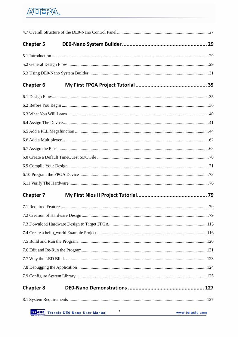
11..22 AAbboouutt tthhee KKIITT
The kit will come with the following contents:
DE0-Nano board
System CD-ROM.
The system CD contains technical documents of the DE0-Nano board, which includes component
datasheets, demonstrations, schematic, and user manual.
Figure 1-2 shows the photograph of the DE0-Nano kit contents.
Figure 1-2 DE0-Nano kit package contents
11..33 GGeettttiinngg HHeellpp
Here is information of how to get help if you encounter any problem:
Terasic Technologies
Tel: +886-3-550-8800
Email: [email protected]

8
Chapter 2
DE0-Nano Board Architecture
This chapter describes the architecture of the DE0-Nano board including block diagram and
components.
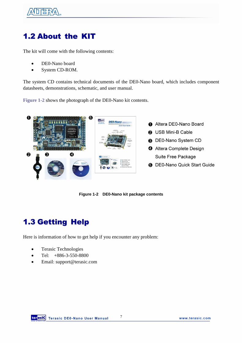
22..11 LLaayyoouutt aanndd CCoommppoonneennttss
The picture of the DE0-Nano board is shown in Figure 2-1 and Figure 2-2. It depicts the layout of
the board and indicates the locations of the connectors and key components.
Figure 2-1 The DE0-Nano Board PCB and component diagram (top view)
9
Figure 2-2 The DE0-Nano Board PCB and component diagram (bottom view)
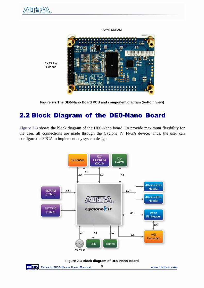
22..22 BBlloocckk DDiiaaggrraamm ooff tthhee DDEE00--NNaannoo BBooaarrdd
Figure 2-3 shows the block diagram of the DE0-Nano board. To provide maximum flexibility for
the user, all connections are made through the Cyclone IV FPGA device. Thus, the user can
configure the FPGA to implement any system design.
Figure 2-3 Block diagram of DE0-Nano Board

10
22..33 PPoowweerr--uupp tthhee DDEE00--NNaannoo BBooaarrdd
The DE0-Nano board comes with a preloaded configuration bit stream to demonstrate the features
of the board. This bit stream also allows users to see quickly if the board is working properly. To
power-up the board two options are available which are described below:
1. Connect a USB Mini-B cable to a USB (Type A) host port and to the board.
2. Alternatively, users can power-up the DE0-Nano board by supplying 5V to the two DC +5
(VCC5) pins of the GPIO headers or supplying (3.6-5.7V) to the 2-pin header. For
communication between the host and the DE0-Nano board, it is necessary to install the Altera
USB Blaster driver software.
At this point you should observe the user LEDs flashing.
11
Chapter 3
Using the DE0-Nano Board
This section describes the detailed information of the components, connectors, and pin assignments
of the DE0-Nano board.
33..11 CCoonnffiigguurriinngg tthhee CCyycclloonnee IIVV FFPPGGAA
The DE0-Nano board contains a serial configuration device that stores configuration data for the
Cyclone IV FPGA. This configuration data is automatically loaded from the configuration device
into the FPGA every time while power is applied to the board. Using the Quartus II software, it is
possible to reconfigure the FPGA at any time, and it is also possible to change the non-volatile data
that is stored in the serial configuration device. Both types of programming methods are described
below.
1. JTAG programming: In this method of programming, named after the IEEE standards Joint
Test Action Group, the configuration bit stream is downloaded directly into the Cyclone IV
FPGA. The FPGA will retain this configuration as long as power is applied to the board; the
configuration information will be lost when the power is turned off.
2. Programming the serial configuration device: In this method, the configuration bit stream is
downloaded into the Altera EPCS16 serial configuration device. It provides non-volatile
storage of the bit stream, so that the information is retained even when the power supply to the
DE0-Nano board is turned off. When the board‘s power is turned on, the configuration data in
the EPCS16 device is automatically loaded into the Cyclone IV FPGA.
JTAG Chain on DE0-Nano Board
The USB-blaster is implemented on the DE0-Nano board to provide JTAG configuration through
onboard USB-to-JTAG configuration logic using a USB Mini-B cable, a FTDI USB 2.0 Controller,
and an Altera MAX II CPLD. Current configuration will be lost when power is turned off.
Figure 3-1 illustrates the JTAG configuration setup.

12
Figure 3-1 JTAG Chain
To download a configuration bit stream file into the Cyclone IV FPGA, perform the following
steps:
Connect a USB Mini-B cable to the Mini-USB Type-AB connector on the DE0-Nano.
The FPGA can now be programmed through the Quartus II Programmer by selecting a
configuration bit stream file with the .sof filename extension.
Configuring the EPCS16
The DE0-Nano board contains an EPCS16 serial configuration device that stores configuration data
for the Cyclone IV device. The Cyclone IV device support in-system programming of a serial
configuration device using the JTAG interface via the serial flash loader design. The serial flash
loader is a bridge design for the Cyclone IV device that uses its JTAG interface to access the
EPCS .jic file and then uses the AS interface to program the EPCS device. Figure 3-2 illustrates the
programming method when adopting a serial flash loader solution.
Figure 3-2 Programming a serial configuration device with serial flash loader solution

13
33..22 GGeenneerraall UUsseerr IInnppuutt//OOuuttppuutt
Push-buttons
The DE0-Nano board contains two push-buttons shown in Figure 3-3 that allow you to interact
with the Cyclone IV device. Each of these switches is debounced using a Schmitt Trigger circuit, as
indicated in Figure 3-4. Each push-button provides a high logic level or a low logic level when it is
not pressed or pressed, respectively.
A CPU reset push-button (KEY0) is an input to the Cyclone IV device. It is intended to be the
master reset signal for FPGA designs loaded into the Cyclone IV device.
Figure 3-3 Connections between the push-buttons and Cyclone IV FPGA
Pushbutton releasedPushbutton depressed
Before
Debouncing
Schmitt Trigger
Debounced
Figure 3-4 Push-buttons debouncing

14
LEDs
The DE0-Nano board consists of 8 green user-controllable LEDs presented in Figure 3-5 to allow
status and debugging signals to be driven to the LEDs from the designs loaded into the Cyclone IV
device. Each LED is driven directly by the Cyclone IV FPGA. The LED is turn on and off when the
associated pins are driven to a high and low logic level, respectively.
Figure 3-5 Connections between the LEDs and Cyclone IV FPGA
DIP Switch
The DE0-Nano board contains a 4 dip switches. When the switch is in the DOWN position or the
UPPER position, it provides a high logic level or a low logic level to the FPGA.
33..33 SSDDRRAAMM MMeemmoorryy
The board features a Synchronous Dynamic Random Access Memory (SDRAM) device providing
32MB with a 16-bit data lines connected to the FPGA. The chip uses 3.3V LVCMOS signaling
standard. All signals are registered on the positive edge of the clock signal, CLK. Figure 3-6
depicts its connection with the Cyclone IV FPGA.

15
Figure 3-6 Connections between FPGA and SDRAM
33..44 II22CC SSeerriiaall EEEEPPRROOMM
A 2Kbit Electrically Erasable PROM (EEPROM) is equipped on the DE0-Nano which is configured
through a 2-wire serial interface. The device is organized as one block of 256 x 8-bit memory. The
I2C write and read address are 0xA0 and 0xA1, respectively. Figure 3-7 illustrates its connection
with the Cyclone IV FPGA.
Figure 3-7 Connections between FPGA and EEPROM

16
33..55 EExxppaannssiioonn HHeeaaddeerrss
The DE0-Nano board consists of two 40-pin expansion headers in Figure 3-8 that offers additional
connectivity and I/Os for general purpose applications. The headers connect directly to 72 pins of
the Cyclone IV FPGA, and also provides two DC +5 (VCC_SYS), two DC +3.3V (VCC3P3), and
four GND pins.
Figure 3-8 Pin distribution of the GPIO expansion headers
33..66 AA//DD CCoonnvveerrtteerr uussiinngg 22xx1133 HHeeaaddeerr
The DE0-Nano contains an ADC128S022 lower power, eight-channel CMOS 12-bit
analog-to-digital converter specified for conversion throughput rates of 50 ksps to 200 ksps. It can
be configured to accept up to eight input signals at inputs IN0 through IN7 located at the 2x13
header shown in Figure 3-9. The I/Os of the 2x13 header are split into 2 banks, one being the
analog input signals (IN0-IN7) and remaining I/Os are connected directly to the Cyclone IV device.
For more detailed information on the A/D converter chip, please refer to its datasheet which is
available on manufacturer‘s website or under the /datasheet folder of the system CD.

17
Figure 3-9 Pin distribution of the 2x13 Header
Figure 3-10 shows the connections on the 2x13 header, A/D converter and Cyclone IV device.
Figure 3-10 Wiring for 2x13 header and A/D converter

18
33..77 DDiiggiittaall AAcccceelleerroommeetteerr
The ADXL345 is a small, thin, ultralow power consumption 3-axis accelerometer with high
resolution measurement. The digital accelerometer is accessed through a SPI 3-wire digital interface.
Digitalized output is formatted as 16-bit twos complement and can be accessed either using SPI
interfac. This chip uses the 3.3V CMOS signaling standard. Main applications include medical
instrumentation, industrial instrumentation, personal electronic aid and hard disk drive protection
etc. Some of the key features of this device are listed below. For more detailed information of better
using this chip, please refer to its datasheet which is available on manufacturer‘s website or under
the /datasheet folder of the system CD.
Up to 13-bit resolution at +/- 16g
SPI (3- wire) digital interface
Flexible interrupts modes
Figure 3-11 shows the connections between ADXL345 and Cyclone IV device.
Figure 3-11 Wiring between the ADXL345 and Cyclone IV device
33..88 CClloocckk CCiirrccuuiittrryy
The DE0-Nano board consists of a 50 MHz oscillator clock connected directly to the dedicated
clock input pin of the Cyclone IV FPGA. The 50MHz clock input can be use as a source clock to
drive the PLL circuit. The clock distribution on the DE0-Nano board is shown in Figure 3-12.

19
Figure 3-12 Block diagram of the clock distribution
33..99 PPoowweerr SSuuppppllyy
The DE0-Nano board‘s power is provided through the USB 5V power or the 5V VCC pins on the
two 40-pin headers or the 2-pin power header. The DC voltage is then stepped down to various
regulators. For portable project applications, connect a battery power supply (3.6~5.7V) to the 2-pin
external power header shown in Figure 3-13.
Figure 3-13 Portable Battery Connection
20
Power Distribution System
Figure 3-14 shows the power distribution system on the DE0-Nano board.
Figure 3-14 DE0-Nano Power Distribution System

21
Chapter 4
DE0-Nano Control Panel
The DE0-Nano board comes with a Control Panel facility that allows users to access various
components on the board from a host computer. The host computer communicates with the board
through a USB connection. The facility can be used to verify the functionality of components on the
board or be used as a debug tool while developing RTL code.
This chapter first presents some basic functions of the Control Panel, then describes its structure in
block diagram form, and finally describes its capabilities.
44..11 CCoonnttrrooll PPaanneell SSeettuupp
The Control Panel Software Utility is located in the directory “tools/DE0_NANO_ControlPanel‖ in
the DE0-Nano System CD. It's free of installation, just copy the whole folder to your host computer
and launch the control panel by executing the ―DE0_NANO_ControlPanel.exe‖.
Specific control circuit should be downloaded to your FPGA board before the control panel can
request it to perform required tasks. The program will call Quartus II tools to download the control
circuit to the FPGA board through USB-Blaster[USB-0] connection.
To activate the Control Panel, perform the following steps:
1. Make sure Quartus II 10.0 or later version is installed successfully on your PC.
2. Connect a USB A to Mini-B cable to a USB (Type A) host port and to the board.
3. Start the executable DE0_NANO_ControlPanel.exe on the host computer. The Control Panel
user interface shown in Figure 4-1 will appear.
5. The DE0_NANO_ControlPanel.sof bit stream is loaded automatically as soon as the
DE0_NANO_ControlPanel.exe is launched.
6. In case the connection is disconnected, click on CONNECT where the .sof will be re-loaded
onto the board.
7. Note, the Control Panel will occupy the USB port until you close that port; you cannot use
Quartus II to download a configuration file into the FPGA until the USB port is closed.

22
8. The Control Panel is now ready for use; experience it by setting the ON/OFF status for some
LEDs and observing the result on the DE0-Nano board.
Figure 4-1 The DE0-Nano Control Panel
The concept of the DE0-Nano Control Panel is illustrated in Figure 4-2. The ―Control Circuit‖ that
performs the control functions is implemented in the FPGA board. It communicates with the
Control Panel window, which is active on the host computer, via the USB Blaster link. The
graphical interface is used to issue commands to the control circuit. It handles all requests and
performs data transfers between the computer and the DE0-Nano board.
23
Figure 4-2 The DE0-Nano Control Panel concept
The DE0-Nano Control Panel can be used to light up LEDs, change the buttons/switches status,
read/write to SDRAM Memory, read ADC channels, and display the Accelerometer information.
44..22 CCoonnttrroolllliinngg tthhee LLEEDDss
A simple function of the Control Panel is to allow setting the values displayed on LEDs. Choosing
the LED tab leads to the window in Figure 4-3. Here, you can directly turn the LEDs on or off
individually or by clicking ―Light All‖ or ―Unlight All‖.
Figure 4-3 Controlling LEDs

24
44..33 SSwwiittcchheess aanndd PPuusshh--bbuuttttoonnss
Choosing the Switches tab leads to the window in Figure 4-4. The function is designed to monitor
the status of slide switches and push-buttons in real time and show the status in a graphical user
interface. It can be used to verify the functionality of the slide switches and push-buttons.
Figure 4-4 Monitoring switches and buttons
The ability to check the status of push-button and slide switch is not needed in typical design
activities. However, it provides users a simple mechanism for verifying if the buttons and switches
are functioning correctly. Thus, it can be used for troubleshooting purposes.
44..44 MMeemmoorryy CCoonnttrroolllleerr
The Control Panel can be used to write/read data to/from the SDRAM/EEPROM/EPCS on the
DE0-Nano board. As an example, we will describe how the SDRAM may be accessed; the same
approach is used to access the EEPROM and EPCS. Click on the Memory tab and select ―SDRAM‖
to reach the window in Figure 4-6.

25
Figure 4-5 Accessing the SDRAM
A 16-bit word can be written into the SDRAM by entering the address of the desired location,
specifying the data to be written, and pressing the Write button. Contents of the location can be read
by pressing the Read button. Figure 4-5 depicts the result of writing the hexadecimal value 06CA
into offset address 200, followed by reading the same location.
The Sequential Write function of the Control Panel is used to write the contents of a file into the
SDRAM as follows:
1. Specify the starting address in the Address box.
2. Specify the number of bytes to be written in the Length box. If the entire file is to be loaded,
then a checkmark may be placed in the File Length box instead of giving the number of bytes.
3. To initiate the writing process, click on the Write a File to Memory button.
4. When the Control Panel responds with the standard Windows dialog box asking for the source
file, specify the desired file in the usual manner.
The Control Panel also supports loading files with a .hex extension. Files with a .hex extension are
ASCII text files that specify memory values using ASCII characters to represent hexadecimal
values. For example, a file containing the line
0123456789ABCDEF
Defines eight 8-bit values: 01, 23, 45, 67, 89, AB, CD, EF. These values will be loaded
consecutively into the memory.

26
The Sequential Read function is used to read the contents of the SDRAM and fill them into a file as
follows:
1. Specify the starting address in the Address box.
2. Specify the number of bytes to be copied into the file in the Length box. If the entire contents
of the SDRAM are to be copied (which involves all 32 Mbytes), then place a checkmark in the
Entire Memory box.
3. Press Load Memory Content to a File button.
4. When the Control Panel responds with the standard Windows dialog box asking for the
destination file, specify the desired file in the usual manner.
Users can use the similar way to access the SDRAM, EEPROM and EPCS. Please note that users
need to erase the EPCS before writing data to it.
44..55 DDiiggiittaall AAcccceelleerroommeetteerr
The Control Panel can be used to display the status of the Digital Accelerometer where it measures
the output of its 3-axis (X, Y, Z). The measurement range is set to ±2g. Figure 4-6 shows the
current digital accelerometer status of the DE0-Nano when Accelerometer tab is clicked.
Figure 4-6 Digital Accelerometer status

27
44..66 AADDCC
From the Control Panel, users are able to read the eight-channel 12-bit analog-to-digital converter.
Figure 4-7 shows the ADC readings when the ADC tab is chosen.
Figure 4-7 ADC Readings
44..77 OOvveerraallll SSttrruuccttuurree ooff tthhee DDEE00--NNaannoo CCoonnttrrooll
PPaanneell
The DE0-Nano Control Panel is based on a Nios II SOPC system instantiated in the Cyclone IV E
FPGA with software running on the on-chip memory. The software part is implemented in C code;
the hardware part is implemented in Verilog HDL code with SOPC builder. The source code is not
available on the DE0-Nano System CD.
To run the Control Panel, users should make the configuration according to Section 3.1. Figure 4-8
depicts the structure of the Control Panel. Each input/output device is controlled by the Nios II
Processor instantiated in the FPGA chip. The communication with the PC is done via the USB
Blaster link. The Nios II interprets the commands sent from the PC and performs the corresponding
actions.

28
Figure 4-8 The block diagram of the DE0-Nano Control Panel

29
Chapter 5
DE0-Nano System Builder
This chapter describes how users can create a custom design project on the DE0-Nano board by
using DE0-Nano Tool – DE0-Nano System Builder.
55..11 IInnttrroodduuccttiioonn
The DE0-Nano System Builder is a Windows based software utility, designed to assist users to
create a Quartus II project for the DE0-Nano board within minutes. The generated Quartus II
project files include:
Quartus II Project File (.qpf)
Quartus II Setting File (.qsf)
Top-Level Design File (.v)
Synopsys Design Constraints file (.sdc)
Pin Assignment Document (.htm)
By providing the above files, DE0-Nano System Builder prevents occurrence of situations that are
prone to errors when users manually edit the top-level design file or place pin assignments. The
common mistakes that users encounter are the following:
1. Board damaged for wrong pin/bank voltage assignments.
2. Board malfunction caused by wrong device connections or missing pin counts for connected
ends.
3. Performance degeneration because of improper pin assignments.
55..22 GGeenneerraall DDeessiiggnn FFllooww
This section will introduce the general design flow to build a project for the DE0-Nano board via
the DE0-Nano System Builder. The general design flow is illustrated in Figure 5-1.
Users should launch DE0-Nano System Builder and create a new project according to their design
requirements. When users complete the settings, the DE0-Nano System Builder will generate two

30
major files which include top-level design file (.v) and Quartus II setting file (.qsf).
The top-level design file contains top-level verilog HDL wrapper for users to add their own
design/logic. The Quartus II setting file contains information such as FPGA device type, top-level
pin assignment, and I/O standard for each user-defined I/O pin.
Finally, Quartus II programmer must be used to download SOF file to DE0-Nano board using JTAG
interface.
Figure 5-1 The general design flow of building a design

31
55..33 UUssiinngg DDEE00--NNaannoo SSyysstteemm BBuuiillddeerr
This section provides the detailed procedures on how the DE0-Nano System Builder is used.
Install and launch the DE0-Nano System Builder
The DE0-Nano System Builder is located in the directory: "Tools\DE0_NANO_SystemBuilder" on
the DE0-Nano System CD. Users can copy the whole folder to a host computer without installing
the utility. Launch the DE0-Nano System Builder by executing the DE0_NANO_SystemBuilder.exe
on the host computer and the GUI window will appear as shown in Figure 5-2.
Figure 5-2 The DE0-Nano System Builder window
Input Project Name
Input project name as show in Figure 5-3.
Project Name: Type in an appropriate name here, it will automatically be assigned as the name of
your top-level design entity.

32
Figure 5-3 The DE0-Nano Board Type and Project Name
System Configuration
Under System Configuration users are given the flexibility of enabling their choice of included
components on the DE0-Nano as shown in Figure 5-4. Each component of the DE0-Nano is listed
where users can enable or disable a component according to their design by simply marking a check
or removing the check in the field provided. If the component is enabled, the DE0-Nano System
Builder will automatically generate the associated pin assignments including the pin name, pin
location, pin direction, and I/O standard.
Figure 5-4 System Configuration Group

33
GPIO Expansion
Users can connect GPIO expansion card onto GPIO header located on the DE0-Nano board as
shown in Figure 5-5. Select the appropriate daughter card you wish to include in your design from
the drop-down menu. The system builder will automatically generate the associated pin assignments
including the pin name, pin location, pin direction, and IO standard.
If a customized daughter board is used, users can select ―GPIO Default‖ followed by changing the
pin name and pin direction according to the specification of the customized daughter board.
Figure 5-5 GPIO Expansion Group
The ―Prefix Name‖ is an optional feature which denotes the prefix pin name of the daughter card
assigned in your design. Users may leave this field empty.
Project Setting Management
The DE0-Nano System Builder also provides functions to restore default setting, loading a setting,
and saving users‘ board configuration file shown in Figure 5-6. Users can save the current board
configuration information into a .cfg file and load it to the DE0-Nano System Builder.

34
Figure 5-6 Project Settings
Project Generation
When users press the Generate button, the DE0-Nano System Builder will generate the
corresponding Quartus II files and documents as listed in the Table 5-1:
Table 5-1 The files generated by DE0-Nano System Builder
No. Filename Description
1 <Project name>.v Top level verilog HDL file for Quartus II
2 <Project name>.qpf Quartus II Project File
3 <Project name>.qsf Quartus II Setting File
4 <Project name>.sdc Synopsys Design Constraints file for Quartus II
5 <Project name>.htm Pin Assignment Document
Users can use Quartus II software to add custom logic into the project and compile the project to
generate the SRAM Object File (.sof).

35
Chapter 6
My First FPGA Project Tutorial
This tutorial provides comprehensive information that will help you understand how to create a
FPGA design and run it on you DE0-Nano development board. The following sections provide a
quick overview of the design flow, explain what you need to get started, and describe what you will
learn.
66..11 DDeessiiggnn FFllooww
Figure 6-1shows the FPGA design flow block diagram.
The standard FPGA design flow starts with design entry using schematics or a hardware description
language (HDL), such as Verilog HDL or VHDL. In this step, you can create a digital circuit that is
implemented inside the FPGA. The flow then proceeds through compilation, simulation,
programming, and verification in the FPGA hardware.
Figure 6-1 Design Flow
This tutorial guides you through all of the steps except for simulation. Although it is not covered in
this document, simulation is very important to learn, and there are entire applications devoted to
simulating hardware designs. There are two types of simulation, Functional and Timing Functional
simulation allows you to verify that your code is manipulating the inputs and outputs appropriately.
Timing (or post place-and-route) simulation verifies that the design meets timing and functions
appropriately in the device.

36
66..22 BBeeffoorree YYoouu BBeeggiinn
This tutorial assumes the following prerequisites
■ You generally know what a FPGA is. This tutorial does not explain the basic concepts of
programmable logic.
■ You are somewhat familiar with digital circuit design and electronic design automation (EDA)
tools.
■ You have installed the Altera Quartus II 10.1 software on your computer. If you do not have the
Quartus II software, you can download it from the Altera web site at www.altera.com/download.
■ You have a DE0-Nano Development Board on which you will test your project. Using a
development board helps you to verify whether your design is really working.
■ You have gone through the quick start guide and/or the getting started user guide for your
development kit. These documents ensure that you have:
Installed the required software.
Determined that the development board functions properly and is connected to your
computer.
Next step you should installed the USB-Blaster driver. Use the USB cable to connect the leftmost
USB connector on the DE0-Nano board to a USB port on a computer that runs the Quartus II
software.
The computer will recognize the new hardware connected to its USB port, but it will be unable to
proceed if it does not have the required driver already installed. The DE0-Nano board is
programmed by using Altera USB-Blaster mechanism. If the USB-Blaster driver is not already
installed, the New Hardware Wizard in Figure 6-2 will appear.

37
Figure 6-2 Found New Hardware Wizard
Since the desired driver is not available on the Windows Update Web site, select ―No, not this time‖
in response to the question asked and click Next. This leads to the window in Figure 6-3.
Figure 6-3 The driver is found in a specific location
38
The driver is available within the Quartus II software. Hence, select Install from a specific location
and click Next to get to Figure 6-4.
Figure 6-4 Specify the location of the driver
Now, choose Search for the best driver in these locations and click Browse to get to the pop-up box
in Figure 6-5 Find the desired driver, which is at location C:\altera\10.1\quartus\drivers\usb-blaster.
Click OK and then upon returning to Figure 6-4 click Next. At this point the installation will
commence, but a dialog box in Figure 6-6 will appear indicating that the driver has not passed the
Windows Logo testing. Click Continue Anyway.

39
Figure 6-5 Browse to find the location
Figure 6-6 There is no need to test the driver

40
The driver will now be installed as indicated in Figure 6-7 Click Finish and you can start using the
DE0-Nano board.
Figure 6-7 The driver is installed
66..33 WWhhaatt YYoouu WWiillll LLeeaarrnn
In this tutorial you will perform the following tasks:
Create a design that causes LEDs on the development board to blink at a speed that is controlled by
an input key—This design is easy to create and gives you visual feedback that the design works. Of
course, you can use your DE0-Nano board to run other designs as well. For the LED design, you
will write Verilog HDL code for a simple 32-bit counter, add a phase-locked loop (PLL)
megafunction as the clock source, and add a 2-input multiplexer megafunction. When the design is
running on the board, you can press an input switch to multiplex the counter bits that drive the
output LEDs.
Develop a foundation to learn more about FPGAs—For example, you can create and download
digital signal processing (DSP) functions onto a single chip, or build a multi-processor system, or
create anything else you can imagine all on the same chip. You don‘t have to scour data books to
find the perfect logic device or create your own ASIC. All you need is your computer, your
imagination, and an Altera DE0-Nano FPGA development board.

41
66..44 AAssssiiggnn TThhee DDeevviiccee
You begin this tutorial by creating a new Quartus II project. A project is a set of files that maintain
information about your FPGA design. The Quartus II Settings File (.qsf) and Quartus II Project File
(.qpf) files are the primary files in a Quartus II project. To compile a design or make pin
assignments, you must first create a project.
In the Quartus II software, select File > New Project Wizard. The Introduction page opens. See
Figure 6-8
Figure 6-8 New Project Wizard introduction
2. Click Next.
3. Enter the following information about your project:
a. What is the working directory for this project? Enter a directory in which you will store your
Quartus II project files for this design.
b. For example, E:\My_design\my_first_fpga.
c. File names, project names, and directories in the Quartus II software cannot contain spaces.

42
d. What is the name of this project? Type my_first_fpga.
e. What is the name of the top-level design entity for this project? Type my_first_fpga. See
Figure 6-9.
Figure 6-9 Project information
f. Click Next.
g. You will assign a specific FPGA device to the design and make pin assignments. See Figure
6-10.

43
Figure 6-10 Specify the Device Example
h. Click Finish.
4. When prompted, choose Yes to create the my_first_fpga project directory. You just created
your first Quartus II FPGA project. See Figure 6-11.

44
Figure 6-11 my_first_fpga project
66..55 AAdddd aa PPLLLL MMeeggaaffuunnccttiioonn
This section describes How to Add a PLL Megafunction
In the design entry step you create a schematic or Block Design File (.bdf) that is the top-level
design. You will add library of parameterized modules (LPM) functions and use Verilog HDL code
to add a logic block. When creating your own designs, you can choose any of these methods or a
combination of them.
1. Choose File > New > Block Diagram/Schematic File (see Figure 6-12 to create a new file,
Block1.bdf, which you will save as the top-level design.

45
Figure 6-12 New BDF
2. Click OK.
3. Choose File > Save As and enter the following information.
File name: my_first_fpga
Save as type: Block Diagram/Schematic File (*.bdf)
4. Click Save. The new design file appears in the Block Editor (see Figure 6-13).

46
Figure 6-13 Bank BDF
5. Add HDL code to the blank block diagram by choosing File > New > Verilog HDL File.
6. Click OK to create a new file Verilog1.v, which you will save as simple_counter.v.
7. Select File > Save As and enter the following information (see Figure 6-14).
File name: simple_counter.v
Save as type: Verilog HDL File (*.v, *.vlg, *.verilog)

47
Figure 6-14 Saving the Verilog HDL file
The resulting empty file is ready for you to enter the Verilog HDL code.
8. Type the following Verilog HDL code into the blank simple_counter.v file (see Figure 6-15
The Verilog File of simple_counter.v).
//It has a single clock input and a 32-bit output port
module simple_counter (
CLOCK_50,
counter_out
);
input CLOCK_50 ;
output [31:0] counter_out;
reg [31:0] counter_out;

48
always @ (posedge CLOCK_50) // on positive clock edge
begin
counter_out <= #1 counter_out + 1;// increment counter
end
endmodule // end of module counter
Figure 6-15 The Verilog File of simple_counter.v
9. Save the file by choosing File > Save, pressing Ctrl + S, or by clicking the floppy disk icon.
10. Choose File > Create/Update > Create Symbol Files for Current File to convert the
simple_counter.v file to a Symbol File (.sym).You use this Symbol File to add the HDL code to
your BDF schematic.
The Quartus II software creates a Symbol File and displays a message (see Figure 6-16).

49
Figure 6-16 Create Symbol File was Successful
11. Click OK.
12. To add the simple_counter.v symbol to the top-level design, click the my_first_fpga.bdf tab.
13. Choose Edit > Insert Symbol.
14. Double-click the Project directory to expand it.
15. Select the newly created simple_counter symbol by clicking it‘s icon.
You can also double-click in a blank area of the BDF to open the Symbol dialog box (If your
Quartus II version is lower than 10.0).
Figure 6-17 Adding the Symbol to the BDF
16. Click OK.
17. Move the cursor to the BDF grid; the symbol image moves with the cursor. Click to place the
simple_counter symbol onto the BDF. You can move the block after placing it by simply
clicking and dragging it to where you want it and releasing the mouse button to place it. See
Figure 6-18.

50
Figure 6-18 Placing the simple_counter symbol
18. Press the Esc key or click an empty place on the schematic grid to cancel placing further
instances of this symbol.
19. Save your project regularly.
Using Quartus Add a PLL Megafunction
Megafunctions, such as the ones available in the LPM, are pre-designed modules that you can use in
FPGA designs. These Altera-provided megafunctions are optimized for speed, area, and device
family. You can increase
Efficiency by using a megafunction instead of writing the function yourself. Altera also provides
more complex functions, called MegaCore functions, which you can evaluate for free but require a
license file for use in production designs. This tutorial design uses a PLL clock source to drive a
simple counter. A PLL uses the on-board oscillator (DE0-Nano Board is 50 MHz) to create a
constant clock frequency as the input to the counter. To create the clock source, you will add a
pre-built LPM megafunction named ALTPLL.
1. Choose Edit > Insert Symbol or click Add Symbol on the toolbar
2. Click Megawizard Plug-in Manager. The MegaWizard® Plug-In Manager appears (see Figure
6-19).

51
Figure 6-19 Mega Wizard Plug-In Manager
3. Click Next.
4. In MegaWizard Plug-In Manager [page 2a], specify the following selections (see Figure 6-20):
a. Choose I/O > ALTPLL.
b. Under Which device family will you be using? Choose the Cyclone IV E for DE0-Nano
development board.
c. Under Which type of output file do you want to create? Choose Verilog HDL.
d. Under What name do you want for the output file? Type pll at the end of the already created
directory name.
e. Click Next.

52
Figure 6-20 MegaWizard Plug-In Manager [page 2a] Selections
5. In the MegaWizard Plug-In Manager [page 3 of 14] window, make the following selections
(see Figure 6-21).
a. Confirm that the Currently selected device family option shows the device family that
corresponds to the development board you are using.
b. The device speed grade choose 6 for DE0-Nano.
c. Set the frequency of the inclock0 input 50 MHz.
d. Click Next.
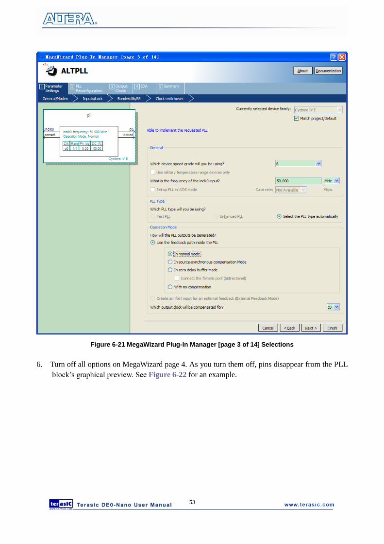
53
Figure 6-21 MegaWizard Plug-In Manager [page 3 of 14] Selections
6. Turn off all options on MegaWizard page 4. As you turn them off, pins disappear from the PLL
block‘s graphical preview. See Figure 6-22 for an example.

54
Figure 6-22 MegaWizard Plug-In Manager [page 4 of 14] Selections
7. Click Next four times.
8. At the top of the wizard, click the tab 3. Output Clocks to jump to the Output Clocks > clk c0
page
Clock Division Settings Figure 6-23).

55
Figure 6-23 MegaWizard Plug-In Manager [page 8 of 14] Selections
9. Click Finish.
10. The wizard displays a summary of the files it creates (see Figure 6-24). Select the pll.bsf
option and click Finish again.

56
Figure 6-24 Wizard-Created Files
The Symbol window opens, showing the newly created PLL megafunction. See Figure 6-25.

57
Figure 6-25 PLL Symbol
11. Click OK and place the pll symbol onto the BDF to the left of the simple_counter symbol. You
can move the symbols around by holding down the left mouse button, helping you ensure that
they line up properly. See Figure 6-26.

58
Figure 6-26 Place the PLL Symbol
12. Move the mouse so that the cursor (also called the selection tool) is over the pll symbol‘s c0
output pin. The orthogonal node tool (cross-hair) icon appears.
13. Click and drag a bus line from the c0 output to the simple_counter clock input. This action ties
the pll output to the simple_counter input (see Figure 6-27).

59
Figure 6-27 Draw a Bus Line connect pll c0 port to simple_counter CLOCK_50 port
14. Add an input pin and an output bus with the following steps:
a. Choose Edit > Insert Symbol.
b. Under Libraries, select quartus/libraries > primitives > pin >input. See Figure 6-28
c. Click OK
If you need more room to place symbols, you can use the vertical and horizontal scroll bars at the
edges of the BDF window to view more drawing space.

60
Figure 6-28 Input pin symbol
d. Place the new pin onto the BDF so that it is touching the input to the pll symbol.
e. Use the mouse to click and drag the new input pin to the left; notice that the ports remain
connected as shown in Figure 6-29.
Figure 6-29 Connecting the PLL symbol and Input port
f. Change the pin name by double-clicking pin_name and typing CLOCK_50 (see Figure 6-30).
This name correlates to the oscillator clock that is connected to the FPGA.
g. Using the Orthogonal Bus tool, draw a bus line connected on one side to the simple_counter
output port, and leave the other end unconnected at about 4 to 8 grid spaces to the right of the
simple_counter.

61
Figure 6-30 Change the input port name
h. Right-click the new output bus line and choose Properties.
i. Using the Orthogonal Bus tool, draw a bus line connected on one side to the simple_counter
output port, and leave the other end unconnected at about 6 to 8 grid spaces to the right of the
simple_counter.
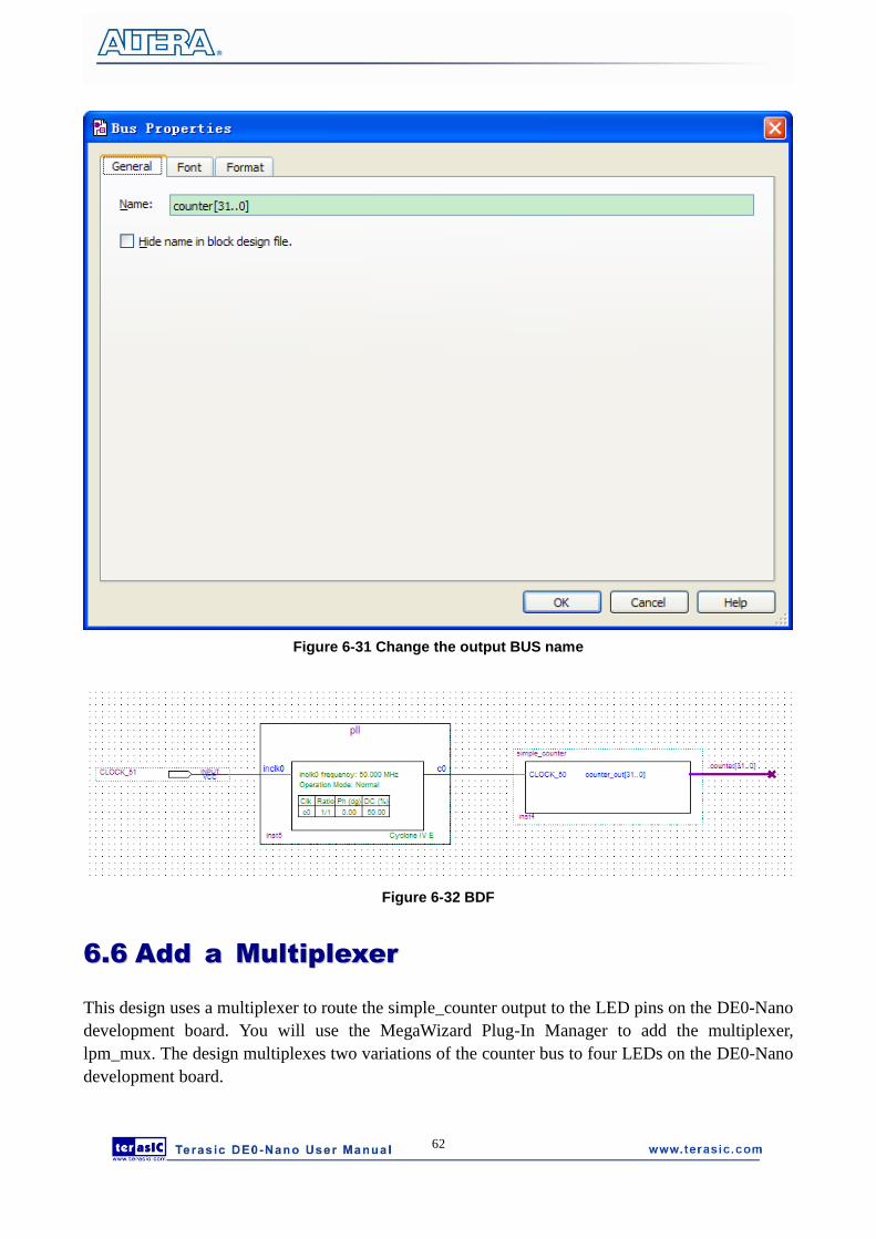
j. Type counter [31..0] as the bus name (see Figure 6-31). The notation [X ..Y] is the Quartus II
method for specifying the bus width in BDF schematics, where X is the most significant bit
(MSB) and Y is the least significant bit (LSB).
k. Click OK. Figure 6-32 shows the BDF.
62
Figure 6-31 Change the output BUS name
Figure 6-32 BDF
66..66 AAdddd aa MMuullttiipplleexxeerr
This design uses a multiplexer to route the simple_counter output to the LED pins on the DE0-Nano
development board. You will use the MegaWizard Plug-In Manager to add the multiplexer,
lpm_mux. The design multiplexes two variations of the counter bus to four LEDs on the DE0-Nano
development board.

63
1. Choose Edit > Insert Symbol.
2. Click Megawizard Plug-in Manager.
3. Click Next.
4. Choose Installed Plug-Ins > Gates > LPM_MUX.
5. Choose the device family that corresponds to the device on the development board you are
using, choose Verilog HDL as the output file type, and name the output file
counter_bus_mux.v (see Figure 6-33).
6. Click Next.
Figure 6-33 Selecting lpm_mux
7. Under How many ‗data‘ inputs do you want? Select 2 inputs (default).
8. Under How ‗wide‘ should the data input and result output be? Select 4 (see Figure 6-34).

64
Figure 6-34 lpm_mux settings
9. Click Next.
10. Click Next, select the counter_bus_mux.bsf options.
11. Click Finish. The Symbol window appears (see Figure 6-35 for an example).
65
Figure 6-35 lpm_mux Symbol
12. Click OK
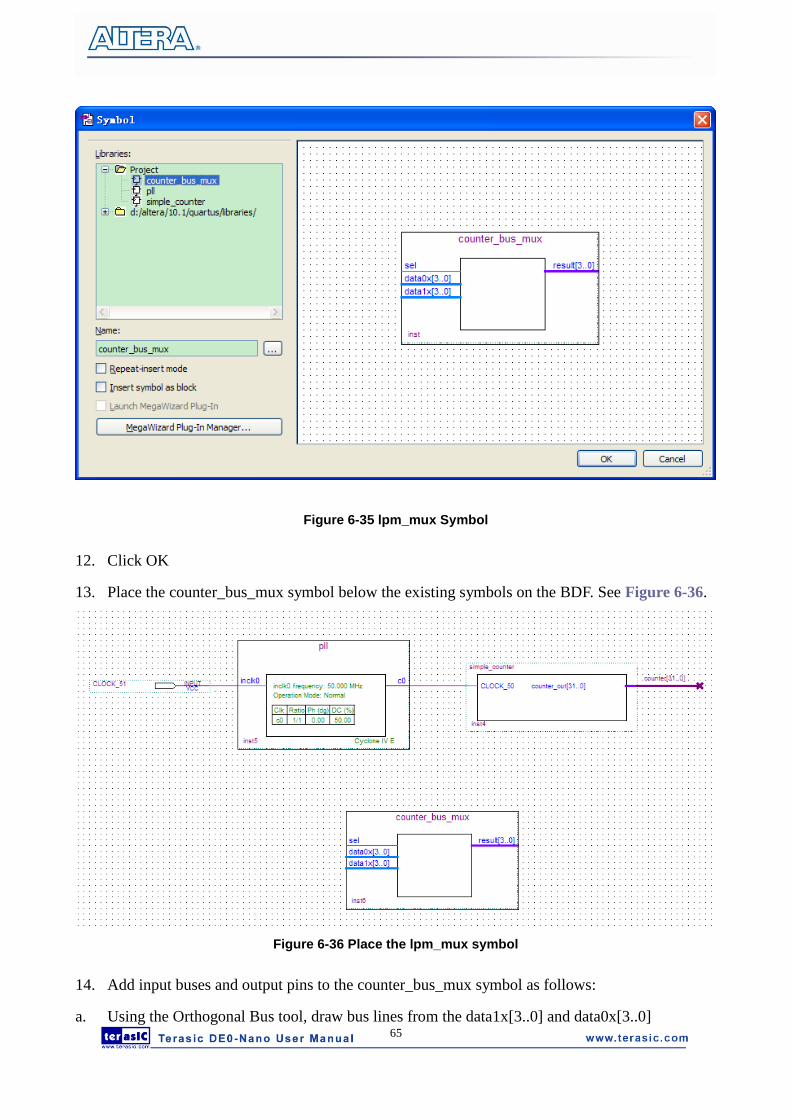
13. Place the counter_bus_mux symbol below the existing symbols on the BDF. See Figure 6-36.
Figure 6-36 Place the lpm_mux symbol
14. Add input buses and output pins to the counter_bus_mux symbol as follows:
a. Using the Orthogonal Bus tool, draw bus lines from the data1x[3..0] and data0x[3..0]

66
Input ports to about 8 to 12 grid spaces to the left of counter_bus_mux.
b. Draw a bus line from the result [3..0] output port to about 4 to 8 grid spaces to the right of
counter_bus_mux.
c. Right-click the bus line connected to data1x[3..0] and choose Properties.
d. Name the bus counter[26..23], which selects only those counter output bits to connect to
the four bits of the data1x input.
Because the input busses to counter_bus_mux have the same names as the output bus from
simple_counter, (counter[x .. y]) the Quartus II software knows to connect these busses.
e. Click OK.
f. Right-click the bus line connected to data0x[3..0] and choose Properties.
g. Name the bus counter [24..21], which selects only those counter output bits to connect to the
four bits of the data1x input.
h. Click OK. Figure 6-37 shows the renamed buses.
Figure 6-37 Renamed counter_bus_mux Bus Lines
If you have not done so already, save your project file before continuing.
15. Choose Edit > Insert Symbol.
16. Under Libraries, double-click quartus/libraries/ > primitives > pin > output (see Figure 6-38).

67
Figure 6-38 choose an output pin
17. Click OK.
18. Place this output pin so that it connects to the counter_bus_mux result [3..0] bus output line.
19. Rename the output pin as LED [3..0] as described in steps 13 c and d. (see Figure 6-39).
Figure 6-39 Rename the output pin
20. Attach an input pin to the multiplexer select line using an input pin:
a. Choose Edit > Insert Symbol.
b. Under Libraries, double-click quartus/libraries/ > primitives > pin > input.
c. Click OK.
21. Place this input pin below counter_bus_mux.
22. Connect the input pin to the counter_bus_mux sel pin.
23. Rename the input pin as KEY [0] (see Figure 6-40).

68
Figure 6-40 Adding the KEY [0] Input Pin
You have finished adding symbols to your design. You can add notes or information to the project
as text using the Text tool on the toolbar (indicated with the A symbol). For example, you can add
the label ―OFF = SLOW, ON = FAST‖ to the KEY [0] input pin and add a project description, such
as ―My First FPGA Project.‖
66..77 AAssssiiggnn tthhee PPiinnss
In this section, you will make pin assignments. Before making pin assignments, perform the
following steps:
1. Choose Processing > Start > Start Analysis & Elaboration in preparation for assigning pin
locations.
2. Click OK in the message window that appears after analysis and elaboration completes.
To make pin assignments that correlate to the KEY [0] and CLOCK_50 input pins and LED[3..0]
output pin, perform the following steps:
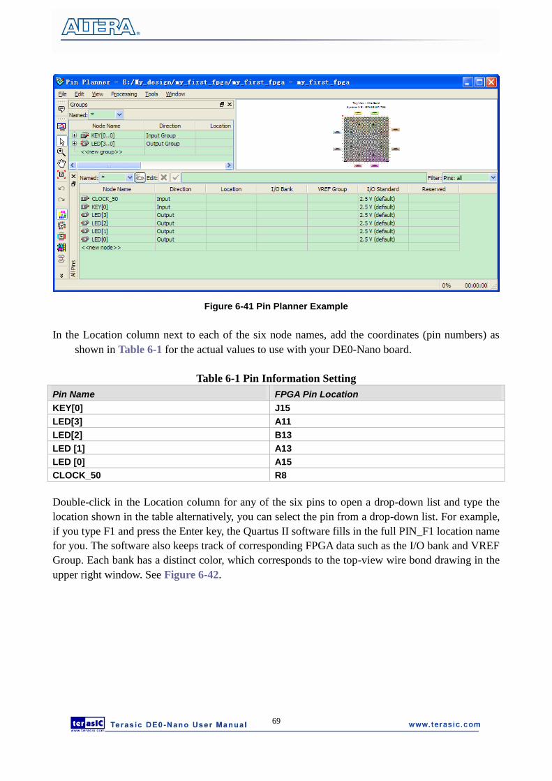
Choose Assignments > Pins, which opens the Pin Planner, a spreadsheet-like table of specific pin
assignments. The Pin Planner shows the design‘s six pins. See Figure 6-41
69
Figure 6-41 Pin Planner Example
In the Location column next to each of the six node names, add the coordinates (pin numbers) as
shown in Table 6-1 for the actual values to use with your DE0-Nano board.
Table 6-1 Pin Information Setting
Pin Name FPGA Pin Location
KEY[0] J15
LED[3] A11
LED[2] B13
LED [1] A13
LED [0] A15
CLOCK_50 R8
Double-click in the Location column for any of the six pins to open a drop-down list and type the
location shown in the table alternatively, you can select the pin from a drop-down list. For example,
if you type F1 and press the Enter key, the Quartus II software fills in the full PIN_F1 location name
for you. The software also keeps track of corresponding FPGA data such as the I/O bank and VREF
Group. Each bank has a distinct color, which corresponds to the top-view wire bond drawing in the
upper right window. See Figure 6-42.

70
Figure 6-42 Completed Pin Planning Example
Now, you are finished creating your Quartus II design!
66..88 CCrreeaattee aa DDeeffaauulltt TTiimmeeQQuueesstt SSDDCC FFiillee
Timing settings are critically important for a successful design. For this tutorial you will create a
basic Synopsys Design Constraints File (.sdc) that the Quartus II TimeQuest Timing Analyzer uses
during design compilation. For more complex designs, you will need to consider the timing
requirements more carefully.
To create an SDC, perform the following steps:
1. Open the TimeQuest Timing Analyzer by choosing Tools > TimeQuest Timing Analyzer.
2. Choose File > New SDC file. The SDC editor opens.
3. Type the following code into the editor:
create_clock -period 20.000 -name CLOCK_50
derive_pll_clocks
derive_clock_uncertainty
4. Save this file as my_first_fpga.sdc (see Figure 6-43)

71
Figure 6-43 Default SDC
Naming the SDC with the same name as the top-level file except for the .sdc extension causes the
Quartus II software to using this timing analysis file automatically by default. If you used another
name, you would need to add the SDC to the assignments file list.
66..99 CCoommppiillee YYoouurr DDeessiiggnn
After creating your design you must compile it. Compilation converts the design into a bitstream
that can be downloaded into the FPGA. The most important output of compilation is an SRAM
Object File (.sof), which you use to program the device. The software also generates other report
files that provide information about your code as it compiles.
If you want to store .SOF in memory device (such as flash or EEPROMs), you must first convert
the SOF to a file type specifically for the targeted memory device.
Now that you have created a complete Quartus II project and entered all assignments, you can
compile the design.
In the Processing menu, choose Start Compilation or click the Play button on the toolbar.

72
If you are asked to save changes to your BDF, click Yes.
While compiling your design, the Quartus II software provides useful information about the
compilation (see Figure 6-44).
Figure 6-44 Compilation Message for project
When compilation is complete, the Quartus II software displays a message. Click OK to close the
message box.
The Quartus II Messages window displays many messages during compilation. It should not display
any critical warnings; it may display a few warnings that indicate that the device timing information
is preliminary or that some parameters on the I/O pins used for the LEDs were not set. The software
provides the compilation results in the Compilation Report tab as shown in Figure 6-45.

73
Figure 6-45 Compilation Report Example
66..1100 PPrrooggrraamm tthhee FFPPGGAA DDeevviiccee
After compiling and verifying your design you are ready to program the FPGA on the development
board. You download the SOF you just created into the FPGA using the USB-Blaster circuitry on
the board. Set up your hardware for programming using the following steps:
For the DE0-Nano board, connect the USB-Blaster (included in your development kit) to J3 and the
USB cable to the USB-Blaster. Connect the other end of the USB cable to the host computer.
Refer to the getting started user guide for detailed instructions on how to connect the cables.
Program the FPGA using the following steps.
1. Choose Tools > Programmer. The Programmer window opens. See Figure 6-46.

74
Figure 6-46 Programmer Window
2. Click Hardware Setup.
3. If it is not already turned on, turn on the USB-Blaster [USB-0] option under currently selected
hardware. See Figure 6-47.

75
Figure 6-47 Hardware Setting
4. Click Close.
5. If the file name in the Programmer does not show my_first_fpga.sof, click Add File.
6. Select the my_first_fpga.sof file from the project directory (see Figure 6-48).

76
Figure 6-48 Downloading Complete
Congratulations, you have created, compiled, and programmed your first FPGA design! The
compiled SRAM Object File (.sof) is loaded onto the FPGA on the development board and the
design should be running.
66..1111 VVeerriiffyy TThhee HHaarrddwwaarree
When you verify the design in hardware, you observe the runtime behavior of the FPGA hardware
design and ensure that it is functioning appropriately.
Verify the design by performing the following steps:
1. Observe that the four development board LEDs appear to be advancing slowly in a binary
count pattern, which is driven by the simple_counter bits [26..23].
The LEDs are active low, therefore, when counting begins all LEDs are turned on (the 0000 state).
2. Press and hold KEY [0] on the development board and observe that the LEDs advance more
quickly. Pressing this KEY causes the design to multiplex using the faster advancing part of
the counter (bits [24..21]).
3. If other LEDs emit faintness light, Choose Assignments > Device. Click Device and Options.
See Figure 6-49.

77
Figure 6-49 Device and Options
Choose unused pins. Reserve all unused pins: Choose the As input tri-stated option. See Figure
6-50.

78
Figure 6-50 Setting unused pins
Click twice OK.
4. In the Processing menu, choose Start Compilation. After the compile, Choose Tools >
Programmer. Select the my_first_fpga.sof file from the project directory. Click Start. At this
time you could find the other LEDs are unlighted.

79
Chapter 7
My First Nios II Project Tutorial
This tutorial provides comprehensive information that will help you understand how to create a
FPGA based SOPC system implementing on your FPGA development board and run software upon
it.
77..11 RReeqquuiirreedd FFeeaattuurreess
The Nios II processor core is a soft-core central processing unit that you could program onto an
Altera field programmable gate array(FPGA). This tutorial illustrates you to the basic flow covering
hardware creation and software building. You are assumed to have the latest Quartus II and NIOS II
EDS software installed and quite familiar with the operation of Windows OS. If you use a different
Quartus II and NIOS II EDS version, there will have some small difference during the operation.
You are also be assumed to possess a DE0-Nano development board (other kinds of dev. Board
based on Altera FPGA chip also supported).
The example NIOS II standard hardware system provides the following necessary components:
Nios II processor core, that‘s where the software will be executed.
On-chip memory to store and run the software
JTAG link for communication between the host computer and target
hardware (typically using a USB-Blaster cable)
LED peripheral I/O (PIO), be used as indicators
77..22 CCrreeaattiioonn ooff HHaarrddwwaarree DDeessiiggnn
This section describes the flow of how to create a hardware system including SOPC feature.
1. Launch Quartus II then select File->New Project Wizard, start to create a new project. See
Figure 7-1 and Figure 7-2.

80
Figure 7-1 Start to Create a New Project
Figure 7-2 New Project Wizard
2. Choose a working directory for this project, type project name and top-level entity name as
shown in Figure 7-3. Then click Next, you will see a window as shown in Figure 7-4.

81
Figure 7-3 Input the working directory, the name of project, top-level design entity
Figure 7-4 New Project Wizard: Add Files [page 2 of 5]
3. Click Next to next window. We choose device family and device settings. You should choose
settings the same as the Figure 7-5. Then click Next to next window as shown in Figure 7-6.

82
Figure 7-5 New Project Wizard: Family & Device Settings [page 3 of 5]
4. Click Next and will see a window as shown in Figure 7-7. Figure 7-7 is a summary about
our new project. Click Finsh to complete project. Figure 7-8 show a new complete project.

83
Figure 7-6 New Project Wizard: EDA Tool Settings [page 4 of 5]
Figure 7-7 New Project Wizard: Summary [page 5 of 5]

84
Figure 7-8 A New Complete Project
5. Choose Tools > SOPC Builder to open new SOPC system wizard .See Figure 7-9 and Figure
7-10.
Figure 7-9 SOPC Builder Menu

85
Figure 7-10 Create New SOPC System [0]
6. Rename System Name as shown in Figure 7-11. Click OK and your will see a window as shown
in Figure 7-12.
Figure 7-11 Create New System [1]

86
Figure 7-12 Create New System[2]
7. Click the Name of the Clock Settings table, rename clk_0 to clk_50. Press Enter to complete the
update. See Figure 7-13.
Figure 7-13 Rename Clock Name
8. Choose Library > Processors > Nios II Processor to open wizard of adding cpu component.
See Figure 7-14 and Figure 7-15.

87
Figure 7-14 Add NIOS II Processor

88
Figure 7-15 Nios II Processor
9. Click Finish to return to main window as shown in Figure 7-16.

89
Figure 7-16 Add Nios II CPU completely
10. Choose cpu_0 and right-click then choose rename, after this, you can update cpu_0 to cpu.
See Figure 7-17 and Figure 7-18.

90
Figure 7-17 Rename CPU name (1)
Figure 7-18 Rename CPU Name (2)

91
11. Choose Library > Interface Protocols > Serial > JTAG UART to open wizard of adding
JTAG UART. See Figure 7-19 and Figure 7-20.
Figure 7-19 Add JTAG UART (1)

92
Figure 7-20 JTAG UART
12. Click Finish to close the wizard and return to the window as shown in Figure 7-21.

93
Figure 7-21 JTAG UART
13. Choose jtag_uart_0 and rename it to jtag_uart as shown in Figure 7-22.

94
Figure 7-22 Rename JTAG UART
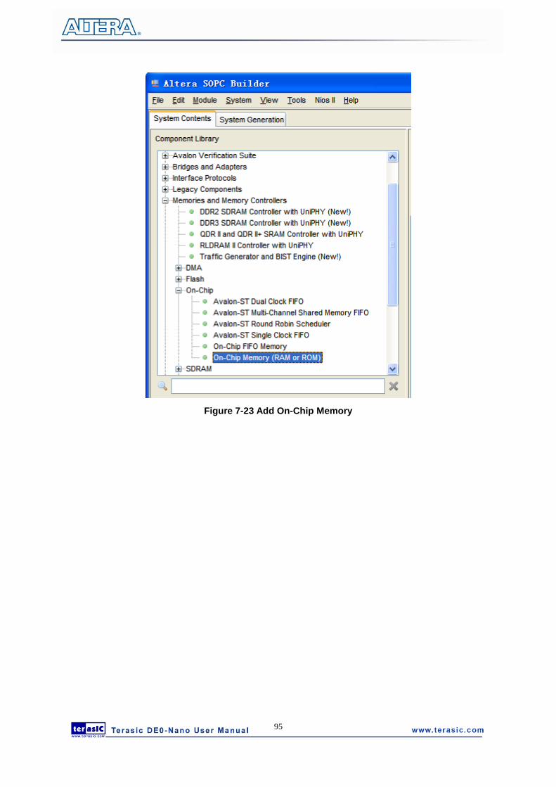
15. Choose Library > Memories and Memory Controllers > On-Chip > On-Chip Memory
(RAM or ROM) to open wizard of adding On-Chip memory. See Figure 7-23 and Figure 7-24.
95
Figure 7-23 Add On-Chip Memory

96
Figure 7-24 On-Chip Memory Box
16. Modify Total memory size to 26000 as shown in Figure 7-25. Click Finish to return to the
window as in Figure 7-26.

97
Figure 7-25 Update Total memory size

98
Figure 7-26 Add On-Chip memory
17. Rename onchip_memory2_0 to onchip_memory2 as shown in Figure 7-27.
Figure 7-27 Rename On-Chip memory
18. Click cpu in the component list on the right part to edit the component. Update Reset vector
and Exception Vector as shown in Figure 7-28. Then click Finish to return to the window as
shown Figure 7-29.

99
Figure 7-28 Update CPU settings

100
Figure 7-29 Update CPU settings Completely
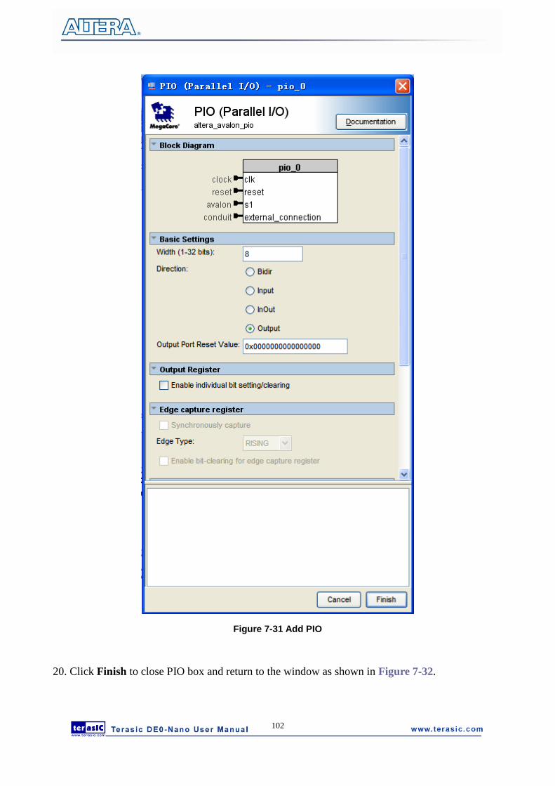
19. Choose Library > Peripherals > Microcontroller Peripherals >PIO (Paralle I/O) to open
wizard of adding PIO. See Figure 7-30 and Figure 7-31.

101
Figure 7-30 Add PIO
102
Figure 7-31 Add PIO
20. Click Finish to close PIO box and return to the window as shown in Figure 7-32.

103
Figure 7-32 PIO
21. Rename pio_0 to pio_led as shown in Figure 7-33.
Figure 7-33 Rename PIO
104
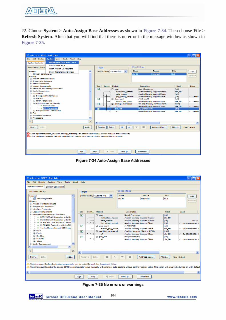
22. Choose System > Auto-Assign Base Addresses as shown in Figure 7-34. Then choose File >
Refresh System. After that you will find that there is no error in the message window as shown in
Figure 7-35.
Figure 7-34 Auto-Assign Base Addresses
Figure 7-35 No errors or warnings

105
23. Click Generate and then pop a window as shown in Figure 7-36. Click Save and at the time a
windows as Figure 7-37 will appear, please input the name and save, then the compilation start. If
there are no errors in the generation, the window will show successful as shown in Figure 7-38.
Figure 7-36 Generate SOPC
Figure 7-37 Generate SOPC
106
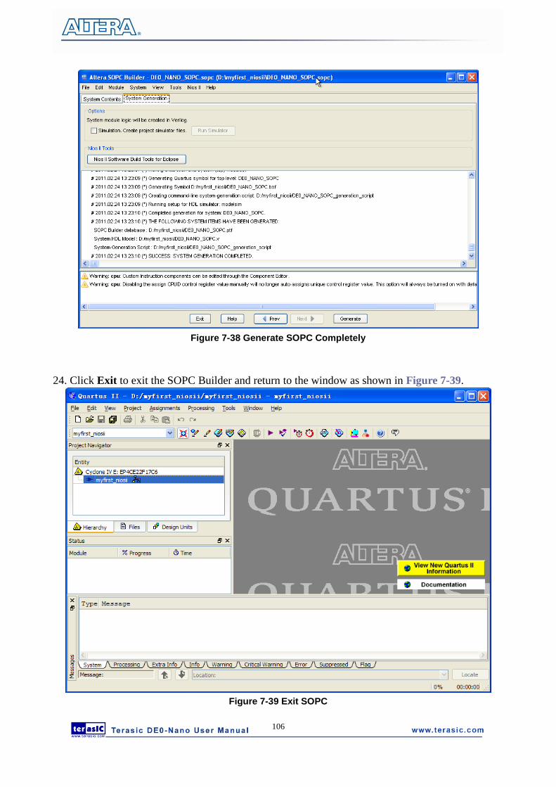
Figure 7-38 Generate SOPC Completely
24. Click Exit to exit the SOPC Builder and return to the window as shown in Figure 7-39.
Figure 7-39 Exit SOPC

107
25. Choose File > New to open new files wizard. See Figure 7-40 and Figure 7-41.
Figure 7-40 New Verilog file
Figure 7-41 New Verilog File

108
33. Choose Verilog HDL File and click OK to return to the window as shown in Figure 7-42.
Figure 7-42 show a blank verilog file.
Figure 7-42 A blank verilog file
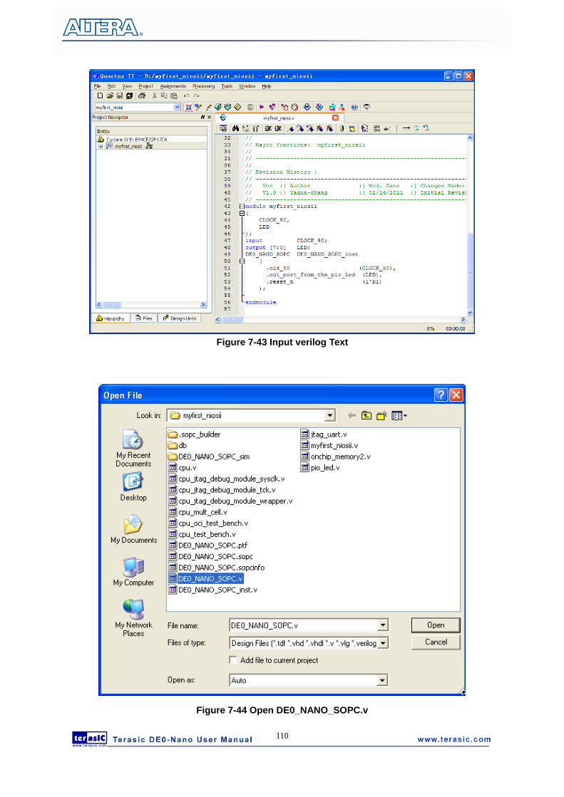
34. Type verilog the following script as shown in Figure 7-43. The module DE0_NANO_SOPC of
the code is from DE0_NANO_SOPC.v of the project. See

109
Figure 7-44 and Figure 7-45.
module myfirst_niosii
(
CLOCK_50,
LED
);
input CLOCK_50;
output [7:0] LED;
DE0_NANO_SOPC DE0_NANO_SOPC_inst
(
.clk_50 (CLOCK_50),
.out_port_from_the_pio_led (LED),
.reset_n (1'b1)
);
endmodule
110
Figure 7-43 Input verilog Text
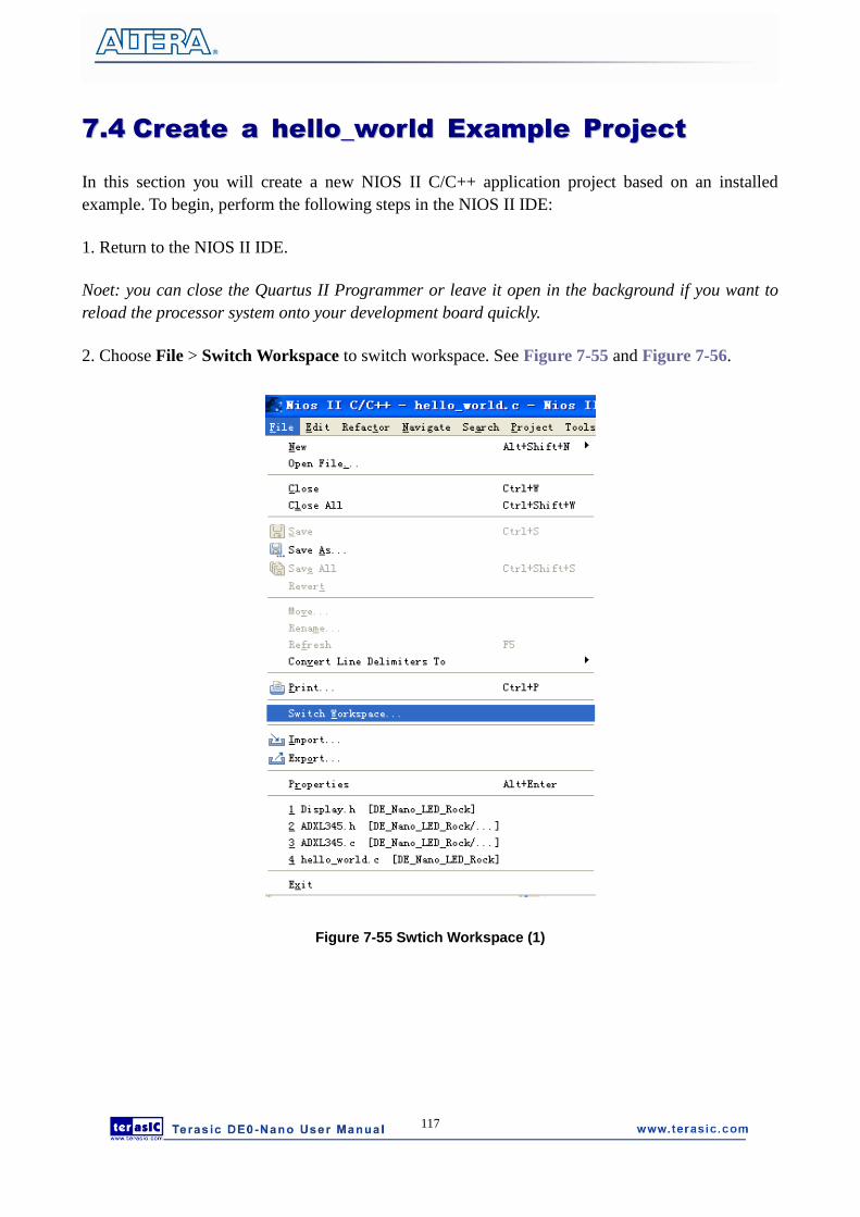
Figure 7-44 Open DE0_NANO_SOPC.v

111
Figure 7-45 DE0_NANO_SOPC module
35. Choose Save Icon in the tool bar. There will appear a window as shown in Figure 7-46. Click
Save.
Figure 7-46 Save Verilog file

112
36. Choose Processing > Start Compilation as shown in Figure 7-47. Figure 7-48 shows the
compilation process.
Figure 7-47 Start Compilation
Figure 7-48 Execute Compile

113
37. A window that shows successfully will appear as shown in Figure 7-49.
Figure 7-49 Compile project completely
45. Choose Assignments > Pins to open pin planner as shown in Figure 7-50. Figure 7-51 show
blank pins.
Figure 7-50 Pins menu

114
Figure 7-51 Blank Pins
46. Input Location value as shown in Figure 7-52.
Figure 7-52 Set Pins
47. Close the pin planner. Restart compilation the project.
77..33 DDoowwnnllooaadd HHaarrddwwaarree DDeessiiggnn ttoo TTaarrggeett FFPPGGAA
This section describes how to download the configuration file to the board.
Download the FPGA configuration file (i.e. the SRAM Object File (.sof) that contains the NIOS II
standard system) to the board by performing the following steps:
1. Connect the board to the host computer via the USB download cable.
2. Apply power to the board.
3. Start the NIOS II IDE.
4. After the welcome page appears, click Workbench.
5. Choose Tools->Quartus II Programmer.
6. Click Auto Detect. The device on your development board should be detected automatically.

115
7. Click the top row to highlight it.
8. Click Change File.
9. Browse to the myfirst_niosii project directory.
10. Select the programming file (myfirst_niosii.sof) for your board.
11. Click OK.
12. Click Hardware Setup in the top, left comer of the Quartus II programmer window. The
Hardware Setup dialog box appears.
13. Select USB-Blaster from the currently selected hardware drop-down list box.
Note: If the appropriate download cable does not appear in the list, you must first install drivers
for the cable. Refer to Quartus II Help for information on how to install the driver. See Figure
7-53.
Figure 7-53 HardWare Setup Window
14. Click Close.
15. Turn on the Program/Configure option for the programming file (see Figure 7-54 for an
example).
16. Click Start.

116
Figure 7-54 Quartus II Programmer
The Progress meter sweeps to 100% after the configuration finished. When configuration is
complete, the FPGA is configured with the Nios II system, but it does not yet have a C program in
memory to execute.
The Nios II IDE build flow is an easy-to-use graphical user interface (GUI) that automates build
and makefile management. The Nios II IDE integrates a text editor, debugger, the Nios II flash
programmer, the Quartus II Programmer, and the Nios II C-to-Hardware (C2H) compiler GUI. The
included example software application templates make it easy for new software programmers to get
started quickly. In this section you will use the Nios II IDE to compile a simple C language example
software program to run on the Nios II standard system configured onto the FPGA on your
development board. You will create a new software project, build it, and run it on the target
hardware. You will also edit the project, re-build it, and set up a debug session.
117
77..44 CCrreeaattee aa hheelllloo__wwoorrlldd EExxaammppllee PPrroojjeecctt
In this section you will create a new NIOS II C/C++ application project based on an installed
example. To begin, perform the following steps in the NIOS II IDE:
1. Return to the NIOS II IDE.
Noet: you can close the Quartus II Programmer or leave it open in the background if you want to
reload the processor system onto your development board quickly.
2. Choose File > Switch Workspace to switch workspace. See Figure 7-55 and Figure 7-56.
Figure 7-55 Swtich Workspace (1)

118
Figure 7-56 Switch Workspace (2)
3. Choose File->New->NIOS II C/C++ Application to open the New Project Wizard.
4. In the New Project wizard, make sure the following things:
a.Select the Hello World project template.
b.Give the project a name. (hello_world_0 is default name)
c.Select the target hardware system PTF file that locates in where the previously created hardware
project resides as shown in Figure 7-57.

119
Figure 7-57 Nios II IDE New Project Wizard
5. Click Finish. The NIOS II IDE creates the hello_world_0 project and returns to the NIOS II
C/C++ project perspective. See Figure 7-58.

120
Figure 7-58 Nios II IDE C++ Project Perspective for hello_world_0
When you create a new project, the NIOS II IDE creates two new projects in the NIOS II C/C++
Projects tab:
■ hello_world_0 is your C/C++ application project. This project contains the source and header
files for your application.
■ hello_world_0_syslib is a system library that encapsulates the details of the Nios II system
hardware.
Note: When you build the system library for the first time the NIOS II IDE automatically generates
files useful for software development, including:
● Installed IP device drivers, including SOPC component device drivers for the NIOS II hardware
system
● Newlib C library, which is a richly featured C library for the NIOS II processor.
● NIOS software packages which includes NIOS II hardware abstraction layer, Nichestack TCP/IP
Network stack, NIOS II host file system, NIOS II read-only zip file system and Micrium‘s μC/OS-II
realtime operating system (RTOS).

121
● system.h, which is a header file that encapsulates your hardware system.
● alt_sys_init.c, which is an initialization file that initializes the devices in the system.
● Hello_world_0.elf, which is an executable and linked format file for the application located in
hello_world_0 folder under Debug.
77..55 BBuuiilldd aanndd RRuunn tthhee PPrrooggrraamm
In this section you will build and run the program to execute the compiled code.
To build the program, right-click the hello_world_0 project in the Nios II C/C++ Projects tab and
choose Build Project. The Build Project dialog box appears and the IDE begins compiling the
project. When compilation completes, a message ‗Build complete‘ will appear in the Console tab.
The compilation time varies depending on your system. See Figure 7-59 for an example.
Figure 7-59 Nios II IDE hello_world_0 Build Completed
Note: If there appears the error which is “region onchip_memory2 is full(hello_world_0.elf
section .text). Region needs to be XXX bytes larger.” , please right-click hello_world_0 ,choose
System Library Properties menu, then pop a window. In the System Library Properties window,
choose Small C Library, then click OK to close the window. Rebuild the project.

122
After compilation complete, right-click the hello_world_0 project, choose Run As , and choose
NIOS II Hardware. The IDE begins to download the program to the target FPGA development
board and begins execution. When the target hardware begins executing the program, the
message ‘Hello from Nios II!‘ appears in the NIOS II IDE Console tab. See Figure 7-60 for an
example.
Figure 7-60 Hello_World_0 Program Output
Now you have created, compiled, and run your first software program based on NIOS II. And you
can perform additional operations such as configuring the system properties, editing and re-building
the application, and debugging the source code.
77..66 EEddiitt aanndd RRee--RRuunn tthhee PPrrooggrraamm
You can modify the hello_world.c program file in the IDE, build it, and re-run the program to
observe your changes executing on the target board. In this section you will add code that will make
LED blink.
Perform the following steps to modify and re-run the program:
1. In the hello_world.c file, add the text shown in blue in the example below:

123
#include <stdio.h>
#include "system.h"
#include "altera_avalon_pio_regs.h"
int main()
{
printf("Hello from Nios II!\n");
int count = 0;
int delay;
while(1)
{
IOWR_ALTERA_AVALON_PIO_DATA(PIO_LED_BASE, count & 0x01);
delay = 0;
while(delay < 2000000)
{
delay++;
}
count++;
}
return 0;
}
2. Save the project.
3. Recompile the file by right-clicking hello_world_0 in the NIOS II C/C++ Projects tab and
choosing Run > Run As > Nios II Hardware.
Note: You do not need to build the project manually; the Nios II IDE automatically re-builds the
program before downloading it to the FPGA.

124
4. Orient your development board so that you can observe LEDG blinking.
77..77 WWhhyy tthhee LLEEDD BBlliinnkkss
The Nios II system description header file, system.h, contains the software definitions, name,
locations, base addresses, and settings for all of the components in the Nios II hardware system. The
system.h file is located in the in the hello_world_0_syslib\Debug\system_description directory as
shown in Figure 7-61.
Figure 7-61 system.h Location
If you look at the system.h file for the Nios II project example used in this tutorial, you will notice
the pio_led function. This function controls the LED. The Nios II processor controls the PIO ports
(and thereby the LED) by reading and writing to the register map. For the PIO, there are four
registers: data, direction, interruptmask, and edgecapture. To turn the LED on and off, the
application writes to the PIO data register.
The PIO core has an associated software file altera_avalon_pio_regs.h. This file defines the core‘s
register map, providing symbolic constants to access the low-level hardware. The
altera_avalon_pio_regs.h file is located in altera\<version
number>\ip\sopc_builder_ip\altera_avalon_pio.
When you include the altera_avalon_pio_regs.h file, several useful functions that manipulate the
PIO core registers are available to your program. In particular, the function
IOWR_ALTERA_AVALON_PIO_DATA(base, data)

125
can write to the PIO data register, turning the LED on and off. The PIO is just one of many SOPC
peripherals that you can use in a system. To learn about the PIO core and other embedded peripheral
cores, refer to Quartus II Version <version> Handbook Volume 5: Embedded Peripherals.
When developing your own designs, you can use the software functions and resources that are
provided with the Nios II HAL. Refer to the Nios II Software Developer‘s Handbook for extensive
documentation on developing your own Nios II processor-based software applications.
77..88 DDeebbuuggggiinngg tthhee AApppplliiccaattiioonn
Before you can debug a project in the NIOS II IDE, you need to create a debug configuration that
specifies how to run the software. To set up a debug configuration, perform the following steps:
1. In the hello_world.c , double-click the front of the line which is needed to set breakpoint. See
Figure 7-62.
Figure 7-62 Set Breakpoint
2. To debug your application, right-click the application (hello_world_0 by default) and choose
Debug as > Nios II Hardware.
3. If the Confirm Perspective Switch message box appears, click Yes.

126
After a moment, the main() function appears in the editor. A blue arrow next to the first line of code
indicates that execution stopped at that line.
5. Choose Run-> Resume to resume execution.
When debugging a project in the Nios II IDE, you can pause, stop or single step the program, set
breakpoints, examine variables, and perform many other common debugging tasks.
Note: To return to the Nios II C/C++ project perspective from the debug perspective, click the two
arrows >> in the top right corner of the GUI.
77..99 CCoonnffiigguurree SSyysstteemm LLiibbrraarryy
In this section you will learn how to configure some advanced options about the target memory or
other things. By performing the following steps, you can charge all the available settings:
1. In the Nios II IDE, right-click hello_world_0 and choose System Library Properties. The
Properties for hello_world_0_syslib dialog box opens.
2. Click System Library. The System Library page contains settings related to how the program
interacts with the underlying hardware. The settings have names that correspond to the targeted
NIOS II hardware.
3. In the Linker Script box, observe which memory has been assigned for Program
memory(.text), Read-only data memory(.rodata), Read/write data memory(.rwdata), Heap
memory, and Stack memory, see Figure 7-63. These settings determine which memory is used to
store the compiled executable program when the example hello_world_0 programs runs. You can
also specify which interface you want to use for stdio , stdin, and stderr. You can also add and
configure an RTOS for your application and configure build options to support C++, reduced device
drivers, etc.
4. Choose onchip_memory2 for all the memory options in the Linker Script box. See Figure 7-63
for an example.

127
Figure 7-63 Configuring System Library Properties
5. Click OK to close the Properties for hello_world_0_syslib dialog box and return to the IDE
workbench.
Note: If you make changes to the system properties you must rebuild your project. To rebuild,
right-click the hello_world_0 project in the Nios II C/C++ Projects tab and choose Build Project.

128
Chapter 8
DE0-Nano Demonstrations
88..11 SSyysstteemm RReeqquuiirreemmeennttss
Make sure Quartus II and NIOS II are installed on your PC.
88..22 BBrreeaatthhiinngg LLEEDDss
In this demonstration, it will show how to use the FPGA to control the luminance of the LEDs by
means of PWM scheme .There are two groups of LEDs, while one group dims, the other group
lights up and vice versa. This behavior acts like a 'human breath'. Users can change the PWM
wave's duty ratio and frequency to control the LED luminance and repetition rate.
Figure 8-1 Shows a diagram of PWM signals to drive LED.

129
Figure 8-2 Pulse Width Modulation
Figure 8-2 shows the relationship between duty cycle and LED luminance.
DDeemmoonnssttrraattiioonn SSoouurrccee CCooddee
Project directory: DE0_NANO_Default
Bit stream used: DE0_NANO.sof
DDeemmoonnssttrraattiioonn BBaattcchh FFiillee
Demo Batch File Folder: DE0_NANO_Default\demo_batch
The demo batch file includes the following files:
FPGA Configure File: DE0_NANO.sof
DDeemmoonnssttrraattiioonn SSeettuupp
Make sure Quartus II and Nios II are installed on your PC.
Connect USB cable to the DE0-Nano board and install USB Blaster driver if necessary.
Execute the demo batch file ―DE0_NANO.bat‖ under the batch file folder,
DE0_NANO_ Default \demo_batch.

130
88..33 AADDCC RReeaaddiinngg
This section illustrates the steps to evaluate the performance of the 8-channel 12-bit A/D Converter.
A DC 3.3V on the 2x13 header is used to drive the analog signal and by using a trimmer
potentiometer, we are able to adjust voltage range from 0~3.3V. The 12-bit voltage measurements
are indicated on the 8 LEDs. Since there are only 8 LEDs, only bit-4 through bit-11 are represented
on the LEDs.
Design Concept
This section describes the design concepts for this demo. Figure 8-3 shows the block diagram.
Figure 8-3 ADC Reading Block Diagram
The ADC Controller reads the voltage from the A/D converter through the serial interface and
displays its measurement on the LEDs. The on-board dip-switch determines which channel to read
from. Table 8–1 lists the DIP Switch settings and its corresponding ADC channel.

131
Table 8–1 DIP Switch Settings
DIP Switch (SW1) Setting ADC Channel
0000 Analog_In0
0001 Analog_In1
0010 Analog_In2
0011 Analog_In3
0100 Analog_In4
0101 Analog_In5
0110 Analog_In6
0111 Analog_In7
Figure 8-4 depicts the pin distribution of the 2X13 header. Connect the trimmer to the ADC
channel to read from (Analog_In0 ~ Analog_In7).

132
Figure 8-4 2X13 Header
System Requirements
The following items are required for the ADC Reading demonstration
DE0-Nano board x1
Trimmer Potentiometer x1
Wire Strip x3
Hardware Setup
Figure 8-5 shows the hardware setup for the ADC Reading demonstration.

133
Figure 8-5 ADC Reading hardware setup
Note: the setup shown above is connected ADC channel 1.
DDeemmoonnssttrraattiioonn SSoouurrccee CCooddee
Project directory: DE0_NANO_ADC
Bit stream used: DE0_NANO.sof
DDeemmoonnssttrraattiioonn BBaattcchh FFiillee
Demo Batch File Folder: DE0_NANO_ADC\demo_batch
The demo batch file includes the following files:
FPGA Configure File: DE0_NANO.sof
DDeemmoonnssttrraattiioonn SSeettuupp
Make sure Quartus II is installed on your PC.
Connect the trimmer to corresponding ADC channel to read from, as well as the +3.3V
and GND signals.
Adjust the DIP switch according to the ADC channel connected
Connect USB cable to the DE0-Nano board and install USB Blaster driver if necessary.
Execute the demo batch file ―DE0_NANO_ADC.bat‖ under the batch file folder,
DE0_NANO_ADC\demo_batch.
Adjust the voltage using the trimmer and observe the measurements on the LEDs. Note a
fully lit LED bar indicates the voltage is 3.3V and similarly no LED lit indicates 0V.

134
88..44 SSOOPPCC DDeemmoo
This section illustrates how to use the SOPC Builder to establish a SOPC System to provide the
following functions:
Control accelerometer through 3-wire SPI interface
Control analog to digital conversion through 4-wire SPI interface
Access EEPROM memory through I2C interface
Access EPCS memory
System Block Diagram
This section describes the SOPC System Block Diagram of this demo. Figure 8-6 shows the block
diagram.
Figure 8-6 SOPC Block Diagram
A 50 MHz Clock is required for the SOPC System. A NIOS II processor is included in the system
for flow control. The PLL is used to generate clocks, including 100 MHz, 10 MHz and 2MHz. The
NIOS II Processor and SDRAM are running at 100 MHZ. The SDRAM is used to store the NIOS II
Program. The ADC SPI Controller is running at 2 MHz. Other peripheral controller is running at 10

135
MHz. The ADC SPI Controller and the Accelerometer SPI Controller are custom SOPC component.
The source code is located in the ―ip‖ folder under this Quartus project. The other SOPC
components are SOPC Builder build-in components.
KEY
The KEY button is driven by PIO Controller with interrupt enabled. It is design to generate an
interrupt event when users click KEY0 or KEY1. The interrupt event is used to terminate
accelerometer and analog to digital conversion process in this demo.
For default, the interrupt is disabled in PIO Controller. Users can enable it with the parameter
setting as shown in below Figure 8-7.
Figure 8-7 PIO Controller
Accelerometer Control
The accelerometer controller is a custom SOPC component developed by Terasic. The source code
is available under the folder \DE0_NANO_SOPC_DEMO\ip\TARASIC_SPI_3WIRE.
In this demo, the accelerometer is controlled through a 3-wire SPI. Note by default the SPI is a
4-wire interface. Before reading any data from the accelerometer, master should set 1 on the SPI bit

136
in the Register 0x31 – DATA_FORMAT register, as shown in below Figure 8-8, to set the device to
3-wire SPI mode.
Figure 8-8 DATA_FORMAT Register
The data format is configured as 10 bits, right-justify, +/- 2g mode. The output data rate is
configured as 400 HZ. The X/Y/Z value is read using polling mode. Before reading X/Y/Z, the
master needs to make sure data is ready by reading the register 0x30-INT_SOURCE, as shown
below Figure 8-9, and checking the DATA_READY bit. In the demo, multiple-byte read of six
bytes X/Y/Z, register from 0x32 to 0x37, is performed to prevent a change in data between reads of
sequential register. Note, the output data is twos complement with DATAx0 as the least significant
byte and DATAx1 as the most significant byte, where x represent X, Y, or Z.
Figure 8-9 Register 0x30
The SPI timing scheme follows clock polarity (CPOL)=1 and clock phase (CPHA)=1. (CPOL)=1
means the clock is high in idle. (CPHA)=1 means data is captured on clock‘s rising edge and data is
propagated on a falling edge. The timing diagram of 3-wire SPI is shown below Figure 8-10:
Figure 8-10 3-wire SPI Timing Diagram
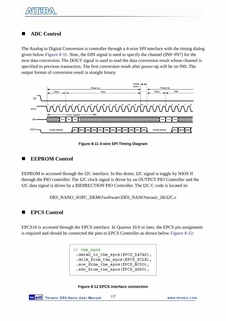
137
ADC Control
The Analog to Digital Conversion is controller through a 4-wire SPI interface with the timing dialog
given below Figure 8-11. Note, the DIN signal is used to specify the channel (IN0~IN7) for the
next data conversion. The DOUT signal is used to read the data conversion result whose channel is
specified in previous transaction. The first conversion result after power-up will be on IN0. The
output format of conversion result is straight binary.
Figure 8-11 4-wire SPI Timing Diagram
EEPROM Control
EEPROM is accessed through the I2C interface. In this demo, I2C signal is toggle by NIOS II
through the PIO controller. The I2C clock signal is driver by an OUTPUT PIO Controller and the
I2C data signal is driver by a BIDIRECTION PIO Controller. The I2C C code is located in:
DE0_NANO_SOPC_DEMO\software\DE0_NANO\terasic_lib\I2C.c
EPCS Control
EPCS16 is accessed through the EPCS interface. In Quartus 10.0 or later, the EPCS pin assignment
is required and should be connected the pins to EPCS Controller as shown below Figure 8-12:
Figure 8-12 EPCS interface connection

138
For the EPCS access functions, users can refer to:
DE0_NANO_SOPC_DEMO\software\DE0_NANO\terasic_lib\Flash.c
DDeemmoonnssttrraattiioonn SSoouurrccee CCooddee
Project directory: DE0_NANO_SOPC_DEMO
Bit stream used: DE0_NANO.sof
NIOS II elf file: DE0_NANO.elf
DDeemmoonnssttrraattiioonn BBaattcchh FFiillee
Demo Batch File Folder: DE0_NANO_SOPC_DEMO\demo_batch
The demo batch file includes the file:
Batch File: test.bat and test_bashrc
FPGA Configure File: DE0_NANO.sof
Nios II Program: DE0_NANO.elf
DDeemmoonnssttrraattiioonn SSeettuupp
Make sure Quartus II and Nios II are installed on your PC.
Connect a USB cable to the DE0-Nano board and install USB Blaster driver if necessary.
Execute the demo batch file ―test.bat‖ under the batch file folder,
DE0_NANO_SOPC_DEMO\demo_batch.
A menu dialog appears as follows:

139
Input ―0‖ to start Accelerometer demo. In the demo, the accelerometer chip ID is shown,
and then X/Y/Z value is displayed every 1.0 second. To terminate the process, just click
KEY0 or KEY1 in the DE0-Nano board.
Menu dialog appears again. Input ―1‖ to start Analog to Digital Conversion Process. In the
demo, the voltage of eight channels is shown repeatedly. To terminate the process, just
click KEY0 or KEY1 in the DE0-Nano board.

140
Menu dialog appears again. Input ―2‖ to start EEPROM Content Dump process. In the
demo, the value of first 16 bytes is dumped. Then, return to the menu dialog.
In the Menu dialog, input ―3‖ to start EPCS demo process. In the demo, the memory size
of EPCS is shown as follows.
88..55 GG--SSeennssoorr
In this demonstration, we illustrate the steps to evaluate the digital accelerometer on the DE0-Nano
board to measure the static acceleration of gravity in tilt-sensing applications. The board can be
tilted from left to right as the digital accelerometer detects any tilting movement and displays it on
the LEDs.
Figure 8-13 DE0-Nano on level surface

141
Design Concept
This section describes the design concepts for this demo. Figure 8-14 shows the block diagram.
Figure 8-14 G-Sensor block diagram
In this demo, the accelerometer is controlled through a 3-wire SPI. Note by default the SPI is a
4-wire interface. Before reading any data from the accelerometer, master should set 1 on the SPI bit
in the Register 0x31 – DATA_FORMAT register. The 3-wire SPI Controller block reads the digital
accelerometer X-axis value and displays the degree scale on the LEDs.
DDeemmoonnssttrraattiioonn SSoouurrccee CCooddee
Project directory: DE0_NANO_GSensor
Bit stream used: DE0_NANO_G_Sensor.sof
DDeemmoonnssttrraattiioonn BBaattcchh FFiillee
Demo Batch File Folder: DE0_NANO_GSensor\demo_batch
The demo batch file includes the following files:
FPGA Configure File: DE0_NANO_G_Sensor.sof

142
DDeemmoonnssttrraattiioonn SSeettuupp
Make sure Quartus II is installed on your PC.
Connect USB cable to the DE0-Nano board and install USB Blaster driver if necessary.
Execute the demo batch file ―test.bat‖ under the batch file folder,
DE0_NANO_GSensor\demo_batch.
Tilt the DE0-Nano board (side to side) and observe the result on the LEDs.
143
Chapter 9
Appendix
99..11 AAppppeennddiixx AA
PPrrooggrraammmmiinngg tthhee SSeerriiaall CCoonnffiigguurraattiioonn DDeevviiccee
This appendix describes how to program the serial configuration device with Serial Flash Loader
(SFL) function via the JTAG interface. User can program serial configuration devices with a JTAG
indirect configuration (.jic) file. To generate JIC programming files with the Quartus II software,
users need to generate a user-specified SRAM object file (.sof), which is the input file first. Next,
users need to convert the SOF to a JIC file. To convert a SOF to a JIC file in Quartus II software,
follow these steps:
Convert SOF to JIC
1. Choose Convert Programming Files (File menu).
2. In the Convert Programming Files dialog box, scroll to the JTAG Indirect Configuration
File (.jic) from the Programming file type field.
3. In the Configuration device field, specify the targeted serial configuration device (please
select EPCS16).
4. In the File name field, browse to the target directory and specify an output file name.
5. Highlight the SOF data in the Input files to convert section. See Figure A1.
6. Click Add File.
7. Select the SOF that you want to convert to a JIC file.
8. Click Open.
144
9. Highlight the Flash Loader and click Add Device. See Figure A2.
10. Click OK. The Select Devices page displays.
Figure A1 Convert Programming Files Dialog Box

145
Figure A2 Highlight Flash Loader
11. Select the targeted FPGA that you are using to program the serial configuration device. See
Figure A3.
12. Click OK. The Convert Programming Files page displays. See Figure A4.
13. Select the .sof file, and Click the Properties. Select Compression, click OK See Figure A5.
14. Click Generate.

146
Figure A3 Select Devices Page
147
Figure A4. Convert Programming Files Page

148
Figure A5 Compression the sof file
Write JIC File into Serial Configuration Device
To program the serial configuration device with the JIC file that you just created, add the file to the
Quartus II Programmer window and follow the steps:
1. When the SOF-to-JIC file conversion is complete, add the JIC file to the Quartus II
Programmer window:
i. Choose Programmer (Tools menu). The Chain1.cdf window displays.
ii. Click Add File. From the Select Programming File page, browse to the JIC file.
iii. Click Open.
2. Program the serial configuration device by checking the corresponding Program/Configure
box, a Factory default SFL image will be load (See Figure A6).

149
Figure A6. Quartus II programmer window with one JIC file
3. Click Start to program serial configuration device.
Erase the Serial Configuration Device
To erase the existed file in the serial configuration device, follow the steps listed below:
1. Choose Programmer (Tools menu). The Chain1.cdf window displays.
2. Click Add File. From the Select Programming File page, browse to a JIC file.
3. Click Open.
4. Erase the serial configuration device by checking the corresponding Erase box, a Factory
default SFL image will be load (See Figure A7).

150
Figure A7 Erasing setting in Quartus II programmer window
5. Click Start to erase the serial configuration device.
151
Chapter 10
Appendix
1100..11 RReevviissiioonn HHiissttoorryy
Version Change Log
V1.0 Initial Version (Preliminary)
1100..22 CCooppyyrriigghhtt SSttaatteemmeenntt
Copyright © 2011 Terasic Technologies. All rights reserved.
Always visit DE0-Nano webpage for new applications.
We will be continuing providing interesting examples and labs on our DE0-Nano webpage. Please
visit www.altera.com or DE0-Nano.terasic.com for more information.