Embed Size (px)
Citation preview
1
DEMO MANUAL DC2554A-A-KIT/DC2554A-B-KIT
Rev. 0
DESCRIPTION
LTC4125 and LT3652HV 650mA Wireless Battery Charger
Demonstration KitDC2554A-KIT is a kit of the DC2556A transmitter, featuring LTC®4125, the DC2555A-A/DC2555A-B receiver, featuring LT3652HV. The DC2555A-A/DC2555A-B receiver can charge a single Li-Ion battery at up to 650mA with an air gap of 3.0mm to 12.0mm between the transmit
All registered trademarks and trademarks are the property of their respective owners.
PERFORMANCE SUMMARY
CONTENTS
BOARD PHOTO
and receive coils. The DC2556A transmitter supports Optimum Power Search and Foreign Object Detection features via LTC4125.
Design files for this circuit board are available.
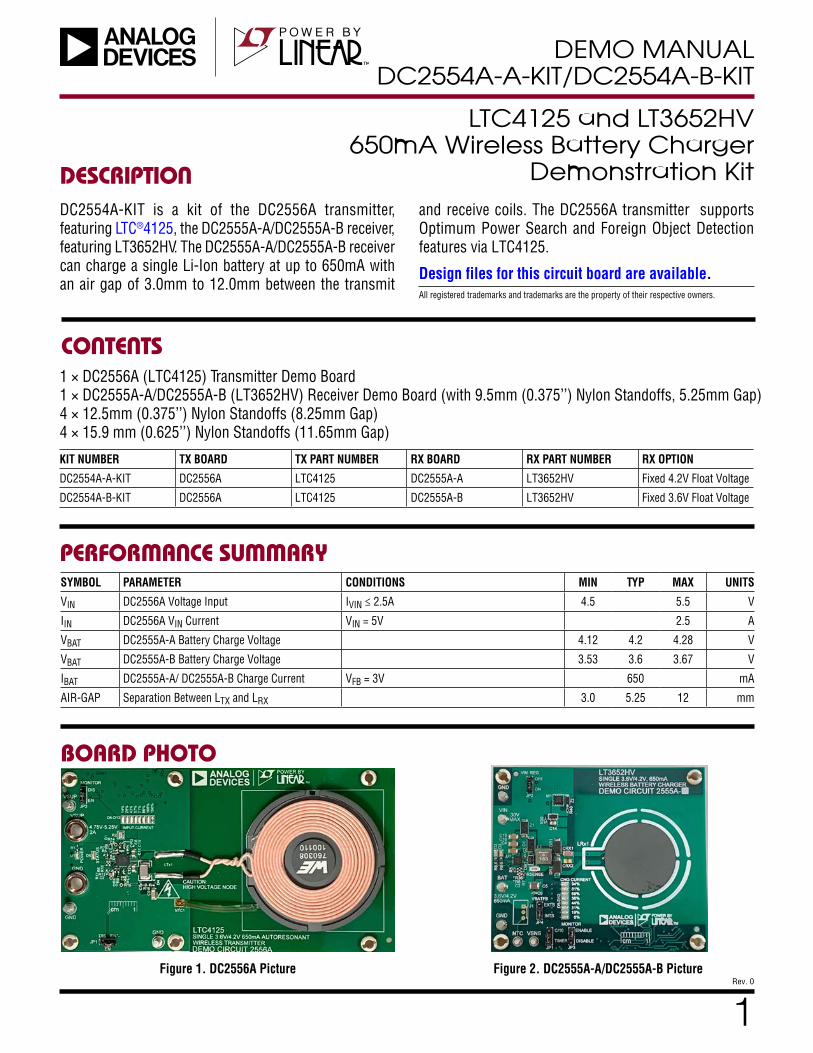
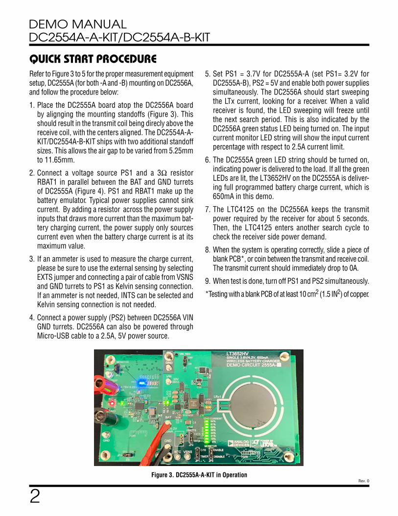
Figure 1. DC2556A Picture Figure 2. DC2555A-A/DC2555A-B Picture
SYMBOL PARAMETER CONDITIONS MIN TYP MAX UNITS
VIN DC2556A Voltage Input IVIN ≤ 2.5A 4.5 5.5 V
IIN DC2556A VIN Current VIN = 5V 2.5 A
VBAT DC2555A-A Battery Charge Voltage 4.12 4.2 4.28 V
VBAT DC2555A-B Battery Charge Voltage 3.53 3.6 3.67 V
IBAT DC2555A-A/ DC2555A-B Charge Current VFB = 3V 650 mA
AIR-GAP Separation Between LTX and LRX 3.0 5.25 12 mm
KIT NUMBER TX BOARD TX PART NUMBER RX BOARD RX PART NUMBER RX OPTION
DC2554A-A-KIT DC2556A LTC4125 DC2555A-A LT3652HV Fixed 4.2V Float Voltage
DC2554A-B-KIT DC2556A LTC4125 DC2555A-B LT3652HV Fixed 3.6V Float Voltage
1 × DC2556A (LTC4125) Transmitter Demo Board 1 × DC2555A-A/DC2555A-B (LT3652HV) Receiver Demo Board (with 9.5mm (0.375’’) Nylon Standoffs, 5.25mm Gap) 4 × 12.5mm (0.375’’) Nylon Standoffs (8.25mm Gap) 4 × 15.9 mm (0.625’’) Nylon Standoffs (11.65mm Gap)
2
DEMO MANUAL DC2554A-A-KIT/DC2554A-B-KIT
Rev. 0
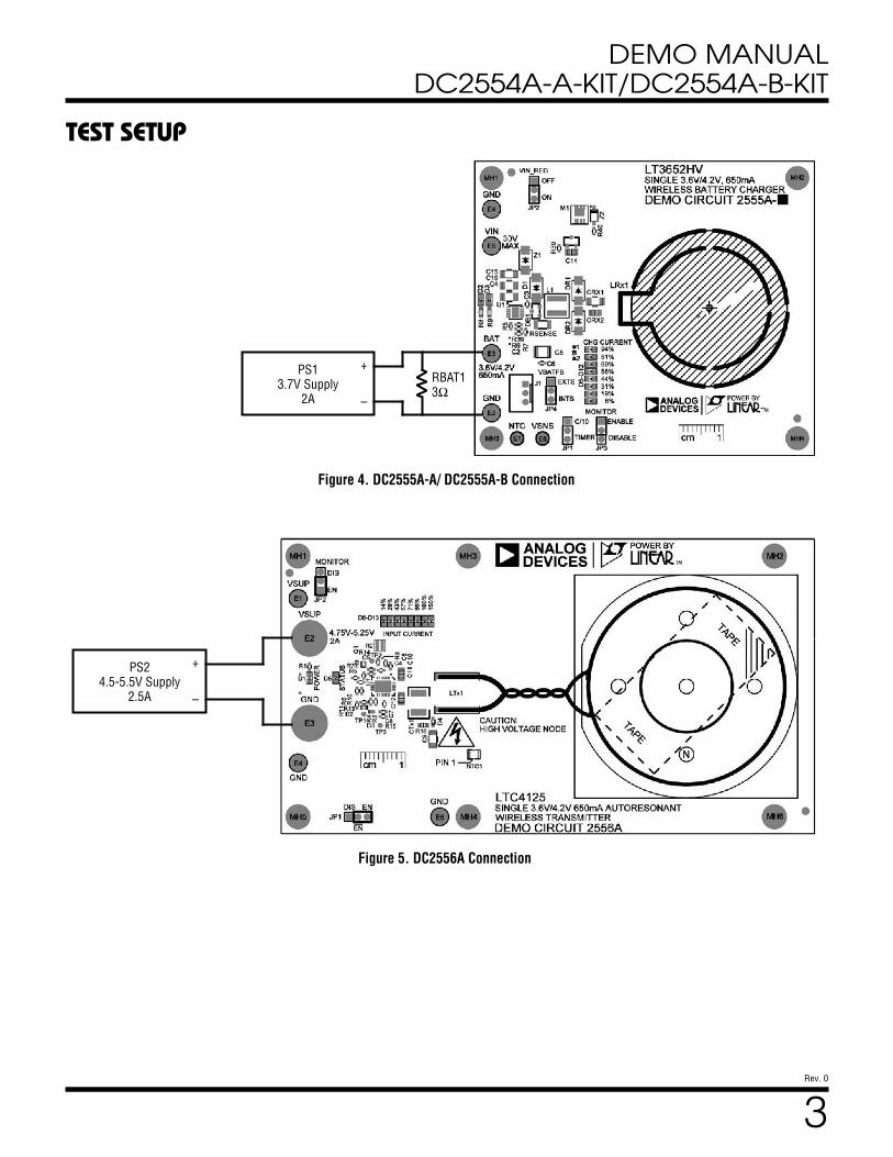
QUICK START PROCEDURERefer to Figure 3 to 5 for the proper measurement equipment setup, DC2555A (for both -A and -B) mounting on DC2556A, and follow the procedure below:
1. Place the DC2555A board atop the DC2556A board by alignging the mounting standoffs (Figure 3). This should result in the transmit coil being direcly above the receive coil, with the centers aligned. The DC2554A-A-KIT/DC2554A-B-KIT ships with two additional standoff sizes. This allows the air gap to be varied from 5.25mm to 11.65mm.
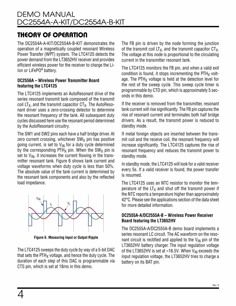
2. Connect a voltage source PS1 and a 3Ω resistor RBAT1 in parallel between the BAT and GND turrets of DC2555A (Figure 4). PS1 and RBAT1 make up the battery emulator. Typical power supplies cannot sink current. By adding a resistor across the power supply inputs that draws more current than the maximum bat-tery charging current, the power supply only sources current even when the battery charge current is at its maximum value.
3. If an ammeter is used to measure the charge current, please be sure to use the external sensing by selecting EXTS jumper and connecting a pair of cable from VSNS and GND turrets to PS1 as Kelvin sensing connection. If an ammeter is not needed, INTS can be selected and Kelvin sensing connection is not needed.
4. Connect a power supply (PS2) between DC2556A VIN GND turrets. DC2556A can also be powered through Micro-USB cable to a 2.5A, 5V power source.
5. Set PS1 = 3.7V for DC2555A-A (set PS1= 3.2V for DC2555A-B), PS2 = 5V and enable both power supplies simultaneously. The DC2556A should start sweeping the LTx current, looking for a receiver. When a valid receiver is found, the LED sweeping will freeze until the next search period. This is also indicated by the DC2556A green status LED being turned on. The input current monitor LED string will show the input current percentage with respect to 2.5A current limit.
6. The DC2555A green LED string should be turned on, indicating power is delivered to the load. If all the green LEDs are lit, the LT3652HV on the DC2555A is deliver-ing full programmed battery charge current, which is 650mA in this demo.
7. The LTC4125 on the DC2556A keeps the transmit power required by the receiver for about 5 seconds. Then, the LTC4125 enters another search cycle to check the receiver side power demand.
8. When the system is operating correctly, slide a piece of blank PCB*, or coin between the transmit and receive coil. The transmit current should immediately drop to 0A.
9. When test is done, turn off PS1 and PS2 simultaneously.
*Testing with a blank PCB of at least 10 cm2 (1.5 IN2) of copper.
Figure 3. DC2555A-A-KIT in Operation
3
DEMO MANUAL DC2554A-A-KIT/DC2554A-B-KIT
Rev. 0
TEST SETUP
Figure 4. DC2555A-A/ DC2555A-B Connection
Figure 5. DC2556A Connection
PS24.5-5.5V Supply
2.5A
+
–
PS13.7V Supply
2A
+
–
RBAT13Ω
4
DEMO MANUAL DC2554A-A-KIT/DC2554A-B-KIT
Rev. 0
THEORY OF OPERATIONThe DC2554A-A-KIT/DC2554A-B-KIT demonstrates the operation of a magnetically coupled resonant Wireless Power Transfer (WPT) system. The LTC4125 detects the power demand from the LT3652HV receiver and provides efficient wireless power for the receiver to charge the Li-Ion or LiFePO4 battery.
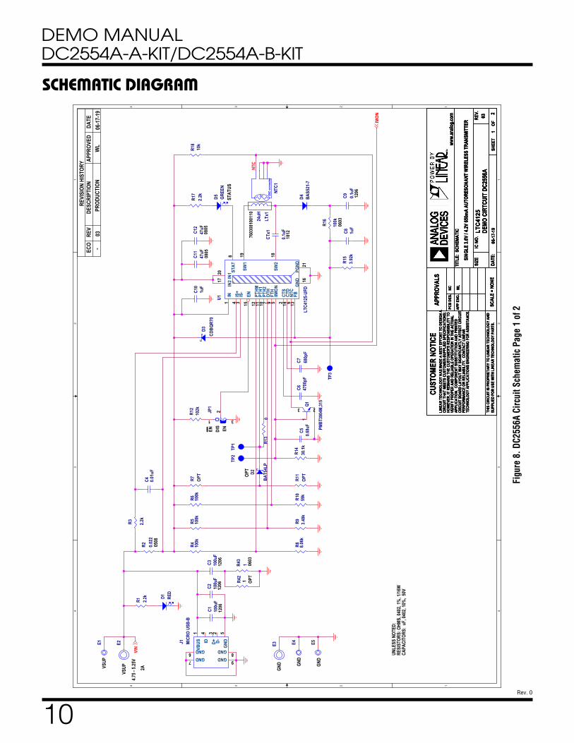
DC2556A – Wireless Power Transmitter Board featuring the LTC4125
The LTC4125 implements an AutoResonant drive of the series resonant transmit tank composed of the transmit coil LTX, and the transmit capacitor CTX. The AutoReso-nant driver uses a zero-crossing detector to determine the resonant frequency of the tank. All subsequent duty cycles discussed here use the resonant period determined by the AutoResonant circuitry.
The SW1 and SW2 pins each have a half bridge driver. At zero current crossing, whichever SWX pin has positive going current, is set to VIN for a duty cycle determined by the corresponding PTHX pin. When the SWX pin is set to VIN, it increases the current flowing in the trans-mitter resonant tank. Figure 6 shows tank current and voltage waveforms when duty cycle is less than 50%. The absolute value of the tank current is determined by the resonant tank components and also by the reflected load impedance.
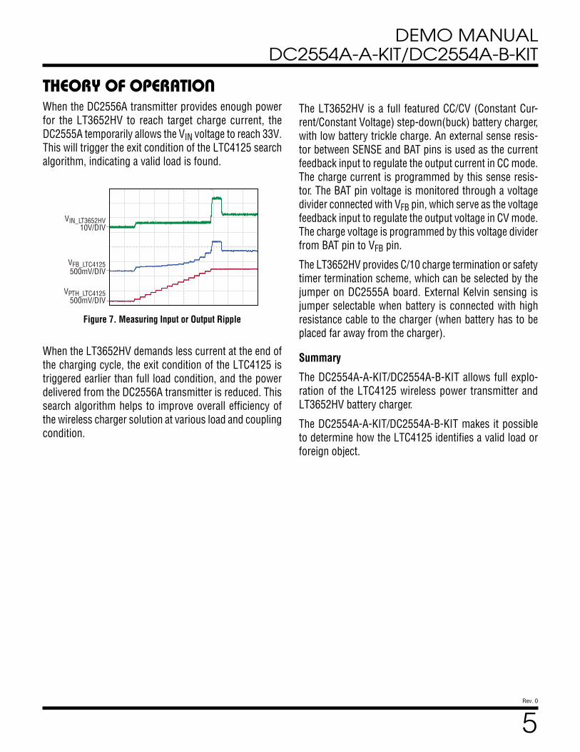
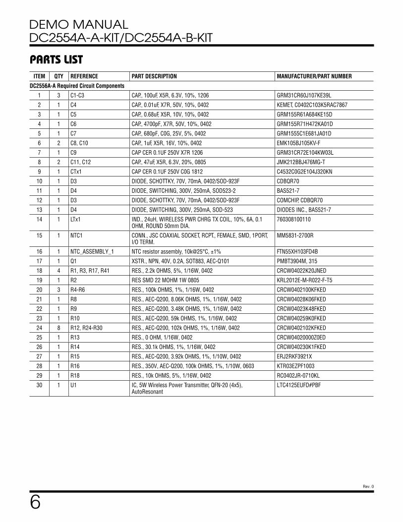
Figure 6. Measuring Input or Output Ripple
VIN
IL VL
The LTC4125 sweeps the duty cycle by way of a 5-bit DAC that sets the PTHX voltage, and hence the duty cycle. The duration of each step of this DAC is programmable via CTS pin, which is set at 18ms in this demo.
The FB pin is driven by the node forming the junction of the transmit coil LTX, and the transmit capacitor CTX. The voltage at this node is proportional to the circulating current in the transmitter resonant tank.
The LTC4125 monitors the FB pin, and when a valid exit condition is found, it stops incrementing the PTHX volt-age. The PTHX voltage is held at the detection level for the rest of the sweep cycle. This sweep cycle timer is programmable by CTD pin, which is approximately 5 sec-onds in this demo.
If the receiver is removed from the transmitter, resonant tank current will rise significantly. The FB pin captures the rise of resonant current and terminates both half bridge drivers. As a result, the transmit power is reduced to standby mode.
If metal foreign objects are inserted between the trans-mit coil and the receive coil, the resonant frequency will increase significantly. The LTC4125 captures the rise of resonant frequency and reduces the transmit power to standby mode.
In standby mode, the LTC4125 will look for a valid receiver every 5s. If a valid receiver is found, the power transfer is resumed.
The LTC4125 uses an NTC resistor to monitor the tem-perature of the LTX and shut off the transmit power if the NTC reports a temperature higher than approximately 42°C. Please see the applications section of the data sheet for more detailed information.
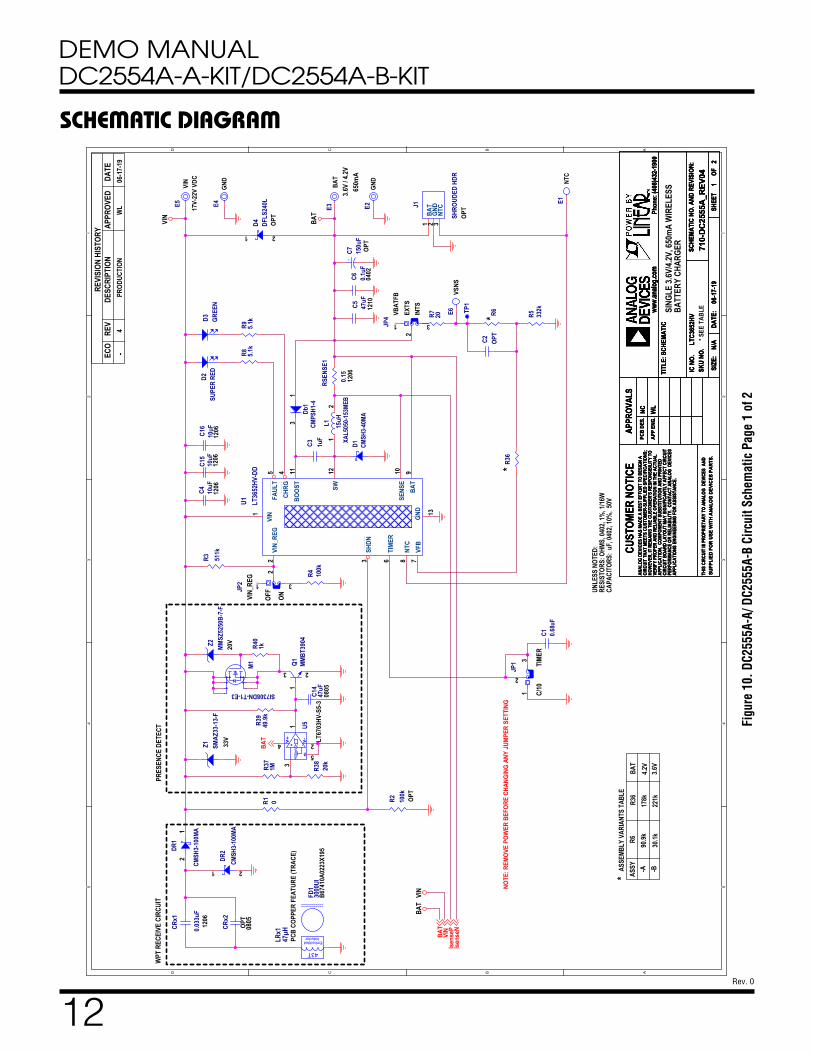
DC2555A-A/DC2555A-B – Wireless Power Receiver Board featuring the LT3652HV
The DC2555A-A/DC2555A-B demo board implements a series resonant LC circuit. The AC waveform on the reso-nant circuit is rectified and applied to the VIN pin of the LT3652HV battery charger. The input regulation voltage of the LT3652HV is set at ≈16.5V. When VIN exceeds the input regulation voltage, the LT3652HV tries to charge a battery on its BAT pin.
5
DEMO MANUAL DC2554A-A-KIT/DC2554A-B-KIT
Rev. 0
THEORY OF OPERATION
Figure 7. Measuring Input or Output Ripple
When the DC2556A transmitter provides enough power for the LT3652HV to reach target charge current, the DC2555A temporarily allows the VIN voltage to reach 33V. This will trigger the exit condition of the LTC4125 search algorithm, indicating a valid load is found.
When the LT3652HV demands less current at the end of the charging cycle, the exit condition of the LTC4125 is triggered earlier than full load condition, and the power delivered from the DC2556A transmitter is reduced. This search algorithm helps to improve overall efficiency of the wireless charger solution at various load and coupling condition.
The LT3652HV is a full featured CC/CV (Constant Cur-rent/Constant Voltage) step-down(buck) battery charger, with low battery trickle charge. An external sense resis-tor between SENSE and BAT pins is used as the current feedback input to regulate the output current in CC mode. The charge current is programmed by this sense resis-tor. The BAT pin voltage is monitored through a voltage divider connected with VFB pin, which serve as the voltage feedback input to regulate the output voltage in CV mode. The charge voltage is programmed by this voltage divider from BAT pin to VFB pin.
The LT3652HV provides C/10 charge termination or safety timer termination scheme, which can be selected by the jumper on DC2555A board. External Kelvin sensing is jumper selectable when battery is connected with high resistance cable to the charger (when battery has to be placed far away from the charger).
Summary
The DC2554A-A-KIT/DC2554A-B-KIT allows full explo-ration of the LTC4125 wireless power transmitter and LT3652HV battery charger.
The DC2554A-A-KIT/DC2554A-B-KIT makes it possible to determine how the LTC4125 identifies a valid load or foreign object.
VPTH_LTC4125500mV/DIV
VFB_LTC4125500mV/DIV
VIN_LT3652HV10V/DIV
6
DEMO MANUAL DC2554A-A-KIT/DC2554A-B-KIT
Rev. 0
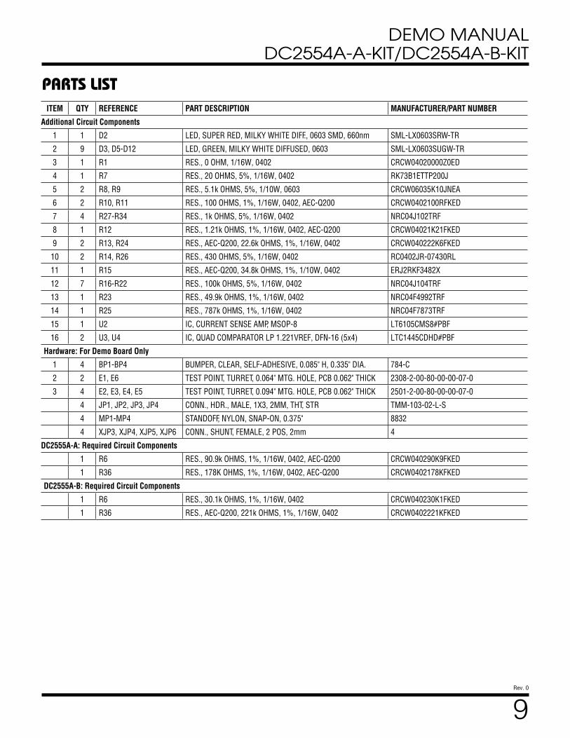
PARTS LISTITEM QTY REFERENCE PART DESCRIPTION MANUFACTURER/PART NUMBER
DC2556A-A Required Circuit Components
1 3 C1-C3 CAP., 100uF, X5R, 6.3V, 10%, 1206 GRM31CR60J107KE39L
2 1 C4 CAP., 0.01uF, X7R, 50V, 10%, 0402 KEMET, C0402C103K5RAC7867
3 1 C5 CAP., 0.68uF, X5R, 10V, 10%, 0402 GRM155R61A684KE15D
4 1 C6 CAP., 4700pF, X7R, 50V, 10%, 0402 GRM155R71H472KA01D
5 1 C7 CAP., 680pF, C0G, 25V, 5%, 0402 GRM1555C1E681JA01D
6 2 C8, C10 CAP., 1uF, X5R, 16V, 10%, 0402 EMK105BJ105KV-F
7 1 C9 CAP CER 0.1UF 250V X7R 1206 GRM31CR72E104KW03L
8 2 C11, C12 CAP., 47uF, X5R, 6.3V, 20%, 0805 JMK212BBJ476MG-T
9 1 CTx1 CAP CER 0.1UF 250V C0G 1812 C4532C0G2E104J320KN
10 1 D3 DIODE, SCHOTTKY, 70V, 70mA, 0402/SOD-923F CDBQR70
11 1 D4 DIODE, SWITCHING, 300V, 250mA, SOD523-2 BAS521-7
12 1 D3 DIODE, SCHOTTKY, 70V, 70mA, 0402/SOD-923F COMCHIP, CDBQR70
13 1 D4 DIODE, SWITCHING, 300V, 250mA, SOD-523 DIODES INC., BAS521-7
14 1 LTx1 IND., 24uH, WIRELESS PWR CHRG TX COIL, 10%, 6A, 0.1 OHM, ROUND 50mm DIA.
760308100110
15 1 NTC1 CONN., JSC COAXIAL SOCKET, RCPT., FEMALE, SMD, 1PORT, I/O TERM.
MM5831-2700R
16 1 NTC_ASSEMBLY_1 NTC resistor assembly, 10k@25°C, ±1% FTN55XH103FD4B
17 1 Q1 XSTR., NPN, 40V, 0.2A, SOT883, AEC-Q101 PMBT3904M, 315
18 4 R1, R3, R17, R41 RES., 2.2k OHMS, 5%, 1/16W, 0402 CRCW04022K20JNED
19 1 R2 RES SMD 22 MOHM 1W 0805 KRL2012E-M-R022-F-T5
20 3 R4-R6 RES., 100k OHMS, 1%, 1/16W, 0402 CRCW0402100KFKED
21 1 R8 RES., AEC-Q200, 8.06K OHMS, 1%, 1/16W, 0402 CRCW04028K06FKED
22 1 R9 RES., AEC-Q200, 3.48K OHMS, 1%, 1/16W, 0402 CRCW04023K48FKED
23 1 R10 RES., AEC-Q200, 59k OHMS, 1%, 1/16W, 0402 CRCW040259K0FKED
24 8 R12, R24-R30 RES., AEC-Q200, 102k OHMS, 1%, 1/16W, 0402 CRCW0402102KFKED
25 1 R13 RES., 0 OHM, 1/16W, 0402 CRCW04020000Z0ED
26 1 R14 RES., 30.1k OHMS, 1%, 1/16W, 0402 CRCW040230K1FKED
27 1 R15 RES., AEC-Q200, 3.92k OHMS, 1%, 1/10W, 0402 ERJ2RKF3921X
28 1 R16 RES., 350V, AEC-Q200, 100k OHMS, 1%, 1/10W, 0603 KTR03EZPF1003
29 1 R18 RES., 10k OHMS, 5%, 1/16W, 0402 RC0402JR-0710KL
30 1 U1 IC, 5W Wireless Power Transmitter, QFN-20 (4x5), AutoResonant
LTC4125EUFD#PBF
7
DEMO MANUAL DC2554A-A-KIT/DC2554A-B-KIT
Rev. 0
PARTS LISTITEM QTY REFERENCE PART DESCRIPTION MANUFACTURER/PART NUMBER
Additional Demo Board Circuit Components
1 3 C13, C15, C16 CAP., 0.01uF, X7R, 50V, 10%, 0402 C0402C103K5RAC7867
2 2 C14, C17 CAP., 1uF, X5R, 16V, 10%, 0402 EMK105BJ105KV-F
3 1 D1 LED, RED, WATER-CLEAR, 0603 LITE-ON, LTST-C193KRKT-5A
4 1 D5 LED, GREEN, WATER CLEAR, 0603 LITE-ON, LTST-C190KGKT
5 7 D6-D12 LED, BLUE, WATER CLEAR, 0603 SML-LXFP0603USBCTR
6 1 R19 RES., 10k OHMS, 5%, 1/16W, 0402 RC0402JR-0710KL
7 2 R20, R33 RES., 430 OHMS, 5%, 1/16W, 0402 RC0402JR-07430RL
8 1 R21 RES., AEC-Q200, 15.4K OHMS, 1%, 1/16W, 0402 CRCW040215K4FKED
9 1 R22 RES., AEC-Q200, 27.4k OHMS, 1%, 1/16W, 0402 CRCW040227K4FKED
10 1 R23 RES., 340k OHMS, 1%, 1/16W, 0402 RC0402FR-07340KL
11 1 R31 RES., AEC-Q200, 11.3k OHMS, 1%, 1/16W, 0402 CRCW040211K3FKED
12 1 R32 RES., 787k OHMS, 1%, 1/16W, 0402 NRC04F7873TRF
13 7 R34-R40 RES., 6.2k OHMS, 1%, 1/16W, 0402 RC0402FR-076K2L
14 1 R43 RES., AEC-Q200, 1 OHM, 5%, 1/10W, 0603 ERJ3GEYJ1R0V
15 2 R20, R33 RES., 430 OHMS, 5%, 1/16W, 0402 RC0402JR-07430RL
16 1 R21 RES., AEC-Q200, 15.4K OHMS, 1%, 1/16W, 0402 CRCW040215K4FKED
Hardware: For Demo Board Only
1 3 E1, E4, E5 TEST POINT, TURRET, 0.094" MTG. HOLE, PCB 0.062" THICK MILL-MAX, 2501-2-00-80-00-00-07-0
2 2 E2, E3 CONN., BANANA JACK, FEMALE, THT, NON-INSULATED, SWAGE, 0.218"
KEYSTONE, 575-4
3 1 J1 CONN., MICRO USB-B, RCPT., FEMALE, 5-PIN, HORZ. R/A SMT WURTH ELEKTRONIK, 629105136821
4 2 JP1, JP2 CONN., HDR., MALE, 1x3, 2mm, THT, STR, NO SUBS. ALLOWED
SAMTEC, TMM-103-02-L-S
5 4 MP1-MP4 STANDOFF, NYLON, SNAP-ON, 0.250" 8831
6 1 NTC ASSEMBLY_1 CONN., JSC COAXIAL SOCKET, RCPT., FEMALE, SMD, 1PORT, I/O TERM.
MURATA, MM5831-2700RB
7 2 XJP1, XJP3 CONN., SHUNT, FEMALE, 2 POS, 2mm WURTH ELEKTRONIK, 60800213421
8
DEMO MANUAL DC2554A-A-KIT/DC2554A-B-KIT
Rev. 0
PARTS LISTITEM QTY REFERENCE PART DESCRIPTION MANUFACTURER/PART NUMBER
DC2555A-A/DC2555A-B: Required Circuit Components
1 1 C1 CAP., 0.68uF, X5R, 10V, 10%, 0402 GRM155R61A684KE15D
2 3 C3, C10, C13 CAP., 1uF, X5R, 16V, 10%, 0402 EMK105BJ105KV-F
4 3 C4, C15, C16 CAP., 10uF, X7R, 50V, 20%, 1206 C3216X5R1H106K160AB
5 1 C5 CAP., 47uF, X5R, 16V, 20%, 1210 1210YD476MAT2A
6 1 C6 CAP., 0.1uF, X5R, 50V, 10%, 0402 GRM155R61H104KE14D
7 4 C8, C9, C11, C12 CAP., 0.01uF, X7R, 50V, 10%, 0402 C0402C103K5RAC7867
8 1 C14 CAP., 47uF, X5R, 6.3V, 20%, 0805 GRM21BR60J476ME15L
9 1 CRX1 CAP., 0.033uF, NP0, 100V, 5%, 1206 C3216NP02A333J160AA
10 1 D1 DIODE, SCHOTTKY RECT., 40V, 3A, SMA CMSH3-40MA TR13 LEAD FREE
11 2 DR1, DR2 DIODE, SCHOTTKY, 100V, 3A, SMA CMSH3-100MA TR13
12 1 DB1 DIODE, SCHOTTKY RECT., 40V, 1.75A, SOT-23F CMPSH1-4 TR LEAD FREE
13 1 FD1 FERRITE, DISC, 26mm DIA X 0.6mm THICK B67410A0223X195
14 1 L1 IND., 15uH, FIXED, 20%, 3.9A XAL5050-153MEC
15 1 M1 XSTR., MOSFET, N-CH, 60V, 6A, PowerPAK 1212-8 Si7308DN-T1-GE3
16 1 Q1 XSTR., NPN, 40V, 200mA, SOT23-3 MMBT3904
17 1 R3 RES., 511k OHMS, 1%, 1/16W, 0402, AEC-Q200 CRCW0402511KFKED
18 1 R4 RES., 100k OHMS, 1%, 1/10W, 0402 ERJ2RKF1003X
19 1 R5 RES., 332k OHMS, 1%, 1/16W, 0402 NRC04F3323TRF
20 1 R37 RES., 20k OHMS, 1%, 1/16W, 0402, AEC-Q200 CRCW040220K0FKED
21 1 R38 RES., 1M OHMS, 1%, 1/16W, 0402, AEC-Q200 CRCW04021M00FKED
22 1 R39 RES., 49.9k OHMS, 1%, 1/16W, 0402 NRC04F4992TRF
23 1 R40 RES., 1k OHMS, 5%, 1/16W, 0402 MCR01MZPF1001
24 1 RSENSE1 RES., 0.15 OHM, 1%, 3/4W, 1206, SHORT-SIDE TERM., AEC-Q200, METAL, SENSE
KRL1632E-M-R150-F-T5
25 1 U1 IC, PWR Tracking 2A Batt.Charger, 3x3 DFN-12 LT3652HVEDD#PBF
26 1 Z1 DIODE, ZENER, 33V, 1W, SMA SMAZ33-13-F
27 1 Z2 DIODE, ZENER, 20V, 500mW, SOD-123 MMSZ5250B-7-F
9
DEMO MANUAL DC2554A-A-KIT/DC2554A-B-KIT
Rev. 0
ITEM QTY REFERENCE PART DESCRIPTION MANUFACTURER/PART NUMBER
Additional Circuit Components
1 1 D2 LED, SUPER RED, MILKY WHITE DIFF., 0603 SMD, 660nm SML-LX0603SRW-TR
2 9 D3, D5-D12 LED, GREEN, MILKY WHITE DIFFUSED, 0603 SML-LX0603SUGW-TR
3 1 R1 RES., 0 OHM, 1/16W, 0402 CRCW04020000Z0ED
4 1 R7 RES., 20 OHMS, 5%, 1/16W, 0402 RK73B1ETTP200J
5 2 R8, R9 RES., 5.1k OHMS, 5%, 1/10W, 0603 CRCW06035K10JNEA
6 2 R10, R11 RES., 100 OHMS, 1%, 1/16W, 0402, AEC-Q200 CRCW0402100RFKED
7 4 R27-R34 RES., 1k OHMS, 5%, 1/16W, 0402 NRC04J102TRF
8 1 R12 RES., 1.21k OHMS, 1%, 1/16W, 0402, AEC-Q200 CRCW04021K21FKED
9 2 R13, R24 RES., AEC-Q200, 22.6k OHMS, 1%, 1/16W, 0402 CRCW040222K6FKED
10 2 R14, R26 RES., 430 OHMS, 5%, 1/16W, 0402 RC0402JR-07430RL
11 1 R15 RES., AEC-Q200, 34.8k OHMS, 1%, 1/10W, 0402 ERJ2RKF3482X
12 7 R16-R22 RES., 100k OHMS, 5%, 1/16W, 0402 NRC04J104TRF
13 1 R23 RES., 49.9k OHMS, 1%, 1/16W, 0402 NRC04F4992TRF
14 1 R25 RES., 787k OHMS, 1%, 1/16W, 0402 NRC04F7873TRF
15 1 U2 IC, CURRENT SENSE AMP, MSOP-8 LT6105CMS8#PBF
16 2 U3, U4 IC, QUAD COMPARATOR LP 1.221VREF, DFN-16 (5x4) LTC1445CDHD#PBF
Hardware: For Demo Board Only
1 4 BP1-BP4 BUMPER, CLEAR, SELF-ADHESIVE, 0.085" H, 0.335" DIA. 784-C
2 2 E1, E6 TEST POINT, TURRET, 0.064" MTG. HOLE, PCB 0.062" THICK 2308-2-00-80-00-00-07-0
3 4 E2, E3, E4, E5 TEST POINT, TURRET, 0.094" MTG. HOLE, PCB 0.062" THICK 2501-2-00-80-00-00-07-0
4 JP1, JP2, JP3, JP4 CONN., HDR., MALE, 1X3, 2MM, THT, STR TMM-103-02-L-S
4 MP1-MP4 STANDOFF, NYLON, SNAP-ON, 0.375" 8832
4 XJP3, XJP4, XJP5, XJP6 CONN., SHUNT, FEMALE, 2 POS, 2mm 4
DC2555A-A: Required Circuit Components
1 R6 RES., 90.9k OHMS, 1%, 1/16W, 0402, AEC-Q200 CRCW040290K9FKED
1 R36 RES., 178K OHMS, 1%, 1/16W, 0402, AEC-Q200 CRCW0402178KFKED
DC2555A-B: Required Circuit Components
1 R6 RES., 30.1k OHMS, 1%, 1/16W, 0402 CRCW040230K1FKED
1 R36 RES., AEC-Q200, 221k OHMS, 1%, 1/16W, 0402 CRCW0402221KFKED
PARTS LIST
10
DEMO MANUAL DC2554A-A-KIT/DC2554A-B-KIT
Rev. 0
SCHEMATIC DIAGRAM4 4
3 3
2 2
1 1
44
33
22
11
UNLE
SS N
OTED
:RE
SIST
ORS:
OHM
S, 04
02, 1
%, 1/
16W
CAPA
CITO
RS: u
F, 04
02, 1
0%, 5
0V
4.75 -
5.25
V
STAT
US
DIS ENEN
OPT
2A
OPT
REVI
SION
HIS
TORY
ECO
DESC
RIPT
ION
REV
DATE
APPR
OVED
-PR
ODUC
TION
06-1
7-19
VSUPVS
UP GND
GND
GND
0508
03W
L
VIN
IMON
SIZE
DATE
:
IC N
O.RE
V.
SHEE
TOF
TITL
E:
APPR
OVAL
S
PCB
DES.
APP
ENG.
CUST
OMER
NOT
ICE
SCHE
MAT
IC
SCAL
E =
NONE
www.
analo
g.com
LINE
AR T
ECHN
OLOG
Y HA
S MA
DE A
BES
T EF
FORT
TO
DESI
GN A
CIRC
UIT
THAT
MEE
TS C
USTO
MER-
SUPP
LIED
SPE
CIFI
CATI
ONS;
HOW
EVER
, IT R
EMAI
NS T
HE C
USTO
MER'
S RE
SPON
SIBI
LITY
TO
VERI
FY P
ROPE
R AN
D RE
LIAB
LE O
PERA
TION
IN T
HE A
CTUA
LAP
PLIC
ATIO
N. C
OMPO
NENT
SUB
STIT
UTIO
N AN
D PR
INTE
DCI
RCUI
T BO
ARD
LAYO
UT M
AY S
IGNI
FICA
NTLY
AFF
ECT
CIRC
UIT
PERF
ORMA
NCE
OR R
ELIA
BILI
TY. C
ONTA
CT L
INEA
RTE
CHNO
LOGY
APP
LICA
TION
S EN
GINE
ERIN
G FO
R AS
SIST
ANCE
.
THIS
CIR
CUIT
IS P
ROPR
IETA
RY T
O LI
NEAR
TEC
HNOL
OGY
AND
SUPP
LIED
FOR
USE
WIT
H LI
NEAR
TEC
HNOL
OGY
PART
S.1
2
NC WL
LTC4125
SING
LE 3.
6V / 4
.2V 65
0mA
AUTO
RESO
NANT
WIR
ELES
S TR
ANSM
ITTE
R
DEMO
CIR
TCUI
T DC
2556
A03
06-1
7-19
T JSC
conn
ecto
r
NTC1
R6 100k
Q1
PMBT
3904
M,31
5
1
3 2
R18
10k
R42
1
C9 0.1u
F12
06
R43
1 0603
J1 MIC
RO U
SB-B
VBUS
1
D-2
D+3
ID4
GND
5
GND 8GND 9GND7
GND6
C4 0.01
uF
R10
59k
TP1
LTx1
24uH
7603
0810
0110
C7 680p
F
C1 100u
F12
06
R2 0.02
2
C12
47uF
0805
C2 100u
F12
06
R12
102k
R8 8.06
kE4
C11
47uF
0805
TP2
C3 100u
F12
06
CTx1
0.1u
F18
12
R7 OPT
C5 0.68u
F
R9 3.48
k
D5 GREE
N
R14
30.1
k
E5
C10
1uF
D2
BAT5
4LP
U1
LTC4
125-
UFD
IN1
16GN
D21
PGND
IN120
IN217
SW1
19
SW2
18
IS-
3IS
+4
FB13
NTC
6
IIMON
5
CTS
2
EN15
CTD
14
STAT
8
PTHM
12PT
H111
PTH2
10DT
H7
FTH
9
TP3
R16
100k
0603
JP1
1 3
2
D4 BAS5
21-7
R17
2.2k
E2
D1 RED
R11
OPT
R13
0
D3CD
BQR7
0
C6 4700
pF
E3
R3 2.2k
R4 100k
R15
3.92
k
E1
C8 1uF
R5 100k
R1 2.2k
NTC
Figu
re 8
. DC2
556A
Circ
uit S
chem
atic
Pag
e 1
of 2
11
DEMO MANUAL DC2554A-A-KIT/DC2554A-B-KIT
Rev. 0
SCHEMATIC DIAGRAM4 4
3 3
2 2
1 1
44
33
22
11
INPU
T CU
RREN
T
1.221
V
DIS
MON
ITOR
U3.3
U2.3
1.186
V
1.186
V
ENA
PCA
ADDI
TION
AL P
ARTS
IMON
VIN
SIZE
DATE
:
IC N
O.RE
V.
SHEE
TOF
TITL
E:
APPR
OVAL
S
PCB
DES.
APP
ENG.
CUST
OMER
NOT
ICE
SCHE
MAT
IC
SCAL
E =
NONE
www.
analo
g.com
LINE
AR T
ECHN
OLOG
Y HA
S MA
DE A
BES
T EF
FORT
TO
DESI
GN A
CIRC
UIT
THAT
MEE
TS C
USTO
MER-
SUPP
LIED
SPE
CIFI
CATI
ONS;
HOW
EVER
, IT R
EMAI
NS T
HE C
USTO
MER'
S RE
SPON
SIBI
LITY
TO
VERI
FY P
ROPE
R AN
D RE
LIAB
LE O
PERA
TION
IN T
HE A
CTUA
LAP
PLIC
ATIO
N. C
OMPO
NENT
SUB
STIT
UTIO
N AN
D PR
INTE
DCI
RCUI
T BO
ARD
LAYO
UT M
AY S
IGNI
FICA
NTLY
AFF
ECT
CIRC
UIT
PERF
ORMA
NCE
OR R
ELIA
BILI
TY. C
ONTA
CT L
INEA
RTE
CHNO
LOGY
APP
LICA
TION
S EN
GINE
ERIN
G FO
R AS
SIST
ANCE
.
THIS
CIR
CUIT
IS P
ROPR
IETA
RY T
O LI
NEAR
TEC
HNOL
OGY
AND
SUPP
LIED
FOR
USE
WIT
H LI
NEAR
TEC
HNOL
OGY
PART
S.2
2
NC WL
LTC4125
BAR
GRAP
H FO
R AU
TORE
SONA
NT W
IREL
ESS
TRAN
SMIT
TER
DEMO
CIR
TCUI
T DC
2556
A03
06-0
5-19
U3E
LTC1
445-
DHD
8REF
9V-
D9 BLUE
R39
6.2k
R25
102k
STNC
L1TO
OL, S
TENC
IL, 7
00-D
C255
6ARE
V03
U2E
LTC1
445-
DHD
8REF
9V-
C17
1uF
C13
0.01
uF
D10
BLUE
R38
6.2k
R26
102k
D11
BLUE
R37
6.2k
R27
102k
C14
1uF
U3A
LTC1
445-
DHD
5 4
149
2
3
17
R36
6.2k
D12
BLUE
R28
102k
R21
15.4
k
U2A
LTC1
445-
DHD
5 4
149
2
3
17
R35
6.2k
C15
0.01
uF
R29
102k
MP1
-MP4
STAN
DOFF
,NYL
ON,S
NAP-
ON,0
.25"
(6.4
mm
)
D13
OPT
R34
6.2k
C16
0.01
uF
R30
102k
U3B
LTC1
445-
DHD
7 6
149
1
3
17
U2B
LTC1
445-
DHD
7 6
149
1
3
17
R32
787k
R23
340k
EPOX
Y AD
HESI
VE,H
EAT
CURE
THE
RMAL
,GRE
Y,30
cc S
YRIN
GE
U3C
LTC1
445-
DHD
11 10
149
16
3
17
JP2
13
2
TAPE
,3/4
" x 3
6yds
,DOU
BLE
SIDE
D PO
LYIM
IDE
KAPT
ON
R20
430
R19
10k
U2C
LTC1
445-
DHD
11 10
149
16
3
17
LB1
LABE
L
D6 BLUE
NTC_
ASSE
MBL
Y_1
RES.
,10k
OHM
S,1%
,NTC
THE
RMIS
TOR
R41
2.2k
R22
27.4
k
R33
430
U3D
LTC1
445-
DHD
13 12
149
15
3
17
D7 BLUE
PCB1
PCB,
DC2
556A
REV0
3
U2D
LTC1
445-
DHD
13 12
149
15
3
17
D8 BLUE
R40
6.2k
R31
11.3
k
R24
102k
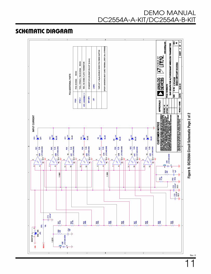
Figu
re 9
. DC2
556A
Circ
uit S
chem
atic
Pag
e 2
of 2
12
DEMO MANUAL DC2554A-A-KIT/DC2554A-B-KIT
Rev. 0
SCHEMATIC DIAGRAM
5 5
4 4
3 3
2 2
1 1
DD
CC
BB
AA
TIME
RC/
10
3.6V
/ 4.2V
WPT
REC
EIVE
CIR
CUIT
UNLE
SS N
OTED
:RE
SIST
ORS:
OHM
S, 04
02, 1
%, 1/
16W
CAPA
CITO
RS: u
F, 04
02, 1
0%, 5
0V
0805
OFF
ONVIN_
REG
VIN
17V-
22V
VDC
GND
BAT
GND NT
C
REVI
SION
HIS
TORY
ECO
REV
DESC
RIPT
ION
APPR
OVED
DATE
WL
06-1
7-19
PROD
UCTI
ON4
-
NOTE
: REM
OVE
POW
ER B
EFOR
E CH
ANGI
NG A
NY J
UMPE
R SE
TTIN
G
OPT
PRES
ENCE
DET
ECT
30.1k
90.9kR6
221kR36
178k
-AASSY
*
-B
**
VSNS
EXTS
INTS SING
LE 3.
6V/4.
2V, 6
50m
A W
IREL
ESS
BATT
ERY
CHAR
GER
VBAT
FB
* SEE
TAB
LE
ASSE
MBLY
VAR
IANT
S TA
BLE
BAT
4.2V
3.6V
650m
A
VIN
VIN
BAT
BAT
Isen
seP
Isen
seN
VIN
BAT
BAT
DATE
:SH
EET
OF
TITL
E: S
CHEM
ATIC
APPR
OVAL
SPC
B DE
S.
APP
ENG.
Phon
e: (4
08)4
32-1
900
SIZE
:
SCHE
MAT
IC N
O. A
ND R
EVIS
ION:
CUST
OMER
NOT
ICE
THIS
CIR
CUIT
IS P
ROPR
IETA
RY T
O AN
ALOG
DEV
ICES
AND
SUPP
LIED
FO
R US
E W
ITH
ANAL
OG
DEV
ICES
PAR
TS.
www.
analo
g.com
SKU
NO.
IC N
O.
ANAL
OG D
EVIC
ES H
AS M
ADE
A BE
ST E
FFOR
T TO
DES
IGN
ACI
RCUI
T TH
AT M
EETS
CUS
TOME
R-SU
PPLI
ED S
PECI
FICA
TION
S;HO
WEV
ER, IT
REM
AINS
THE
CUS
TOME
R'S
RESP
ONSI
BILI
TY T
OVE
RIFY
PRO
PER
AND
RELI
ABLE
OPE
RATI
ON IN
THE
ACT
UAL
APPL
ICAT
ION.
COM
PONE
NT S
UBST
ITUT
ION
AND
PRIN
TED
CIRC
UIT
BOAR
D LA
YOUT
MAY
SIG
NIFI
CANT
LY A
FFEC
T CI
RCUI
TPE
RFOR
MANC
E OR
REL
IABI
LITY
. CON
TACT
ANA
LOG
DEV
ICES
APPL
ICAT
IONS
ENG
INEE
RING
FOR
ASS
ISTA
NCE.
12
NC WL
LTC3
652H
V710-DC2555A_REV04
N/A
06-1
7-19
Z2 MM
SZ52
50B-
7-F
20V
R37
1M
NC
V+
V-
400mV+ -
U5
LT67
03HV
-S5-
3
2
3
45
1
R2 100k
C5 47uF
1210
C2 OPT
C14
47uF
0805
R6E6
Embedded Inductor
43T
LRx1
47µH
PCB
COPP
ER F
EATU
RE (T
RACE
)
R1 0
C16
10uF
1206
R7 20
E5
M1
SI7308DN-T1-E3
C15
10uF
1206
CRx1
0.03
3uF
1206
RSEN
SE1
0.15
1206
R4 100k
R39
49.9
k
JP1
13
2
J1
SHRO
UDED
HDR
OPT
BAT
1GN
D2
NTC
3
D1 CMSH
3-40
MA
R3 511k
DR1
CMSH
3-10
0MA
21
+C7 15
0uF
OPT
R40
1k
E1
D3 GREE
N
C1 0.68u
F
Db1
CMPS
H1-4
13
D4 DFLS
240L
OPT
21
R9 5.1k
D2SU
PER
RED
E2
R38
20k
TP1
R36
CRx2
OPT
C3 1uF
C6 0.1u
F04
02
JP2 1 3
2
E3
Q1 MM
BT39
04
3 2
1
U1 LT36
52HV
-DD
VIN_
REG
2
SHDN
3
BOOS
T11
FAUL
T5
VFB
7
CHRG
4
BAT
9NT
C8
VIN1
TIM
ER6
SW12
SENS
E10
GND 13
R5 332k
L1 15uH
XAL5
050-
153M
EB
12
C4 10uF
1206
DR2
CMSH
3-10
0MA
21
FD1
3000
UIB6
7410
A022
3X19
5
R8 5.1k
Z1 SMAZ
33-1
3-F
33V
JP4
1 3
2
E4
Figu
re 1
0. D
C255
5A-A
/ DC2
555A
-B C
ircui
t Sch
emat
ic P
age
1 of
2
13
DEMO MANUAL DC2554A-A-KIT/DC2554A-B-KIT
Rev. 0
Information furnished by Analog Devices is believed to be accurate and reliable. However, no responsibility is assumed by Analog Devices for its use, nor for any infringements of patents or other rights of third parties that may result from its use. Specifications subject to change without notice. No license is granted by implication or otherwise under any patent or patent rights of Analog Devices.
SCHEMATIC DIAGRAM
5 5
4 4
3 3
2 2
1 1
44
33
22
11
UNLE
SS N
OTED
:RE
SIST
ORS:
OHM
S, 04
02, 1
%, 1/
16W
CAPA
CITO
RS: u
F, 04
02, 1
0%, 5
0V
1.221
V
U4.3
U3.3
1.186
V
1.186
V
CHAR
GE C
URRE
NT
DISA
BLE
MON
ITOR
ENAB
LE
94%
81%
69%
56%
44%
31%
19% 6%
PCA
ADDI
TION
AL P
ARTS
BAR
GRAP
H FO
R SI
NGLE
3.6V
/ 4.2V
, 650
mA
WIR
ELES
S BA
TTER
Y CH
ARGE
R
* SEE
TAB
LE
VIN BA
T
Isen
seP
Isen
seN
DATE
:SH
EET
OF
TITL
E: S
CHEM
ATIC
APPR
OVAL
SPC
B DE
S.
APP
ENG.
Phon
e: (4
08)4
32-1
900
SIZE
:
SCHE
MAT
IC N
O. A
ND R
EVIS
ION:
CUST
OMER
NOT
ICE
THIS
CIR
CUIT
IS P
ROPR
IETA
RY T
O AN
ALOG
DEV
ICES
AND
SUPP
LIED
FO
R US
E W
ITH
ANAL
OG
DEV
ICES
PAR
TS.
www.
analo
g.com
SKU
NO.
IC N
O.
ANAL
OG D
EVIC
ES H
AS M
ADE
A BE
ST E
FFOR
T TO
DES
IGN
ACI
RCUI
T TH
AT M
EETS
CUS
TOME
R-SU
PPLI
ED S
PECI
FICA
TION
S;HO
WEV
ER, IT
REM
AINS
THE
CUS
TOME
R'S
RESP
ONSI
BILI
TY T
OVE
RIFY
PRO
PER
AND
RELI
ABLE
OPE
RATI
ON IN
THE
ACT
UAL
APPL
ICAT
ION.
COM
PONE
NT S
UBST
ITUT
ION
AND
PRIN
TED
CIRC
UIT
BOAR
D LA
YOUT
MAY
SIG
NIFI
CANT
LY A
FFEC
T CI
RCUI
TPE
RFOR
MANC
E OR
REL
IABI
LITY
. CON
TACT
ANA
LOG
DEV
ICES
APPL
ICAT
IONS
ENG
INEE
RING
FOR
ASS
ISTA
NCE.
22
NC WL
LTC3
652H
V710-DC2555A_REV04
N/A
06-0
6-19
R18
100k
D5
GREE
N
C8 0.01
uF
R32
1k
D11
GREE
N
R19
100k
PCB1
PCB,
DC2
555A
REV0
4
C10
1uF
R20
100k
R31 1k
U3E
LTC1
445-
DHD
8REF
9V-
D12
GREE
N
R21
100k
D9
GREE
N
R24
22.6
kR2
210
0k
R30 1k
U4E
LTC1
445-
DHD
8REF
9V-
JP3
13
2
U3D
LTC1
445-
DHD
13 12
149
15
3
17
U3C
LTC1
445-
DHD
11 10
149
16
3
17
D8
GREE
N
U3B
LTC1
445-
DHD
7 6
149
1
3
17
D10
GREE
N
R23
49.9
k
R29 1k
U4D
LTC1
445-
DHD
13 12
149
15
3
17
U3A
LTC1
445-
DHD
5 4
149
2
3
17
U4C
LTC1
445-
DHD
11 10
149
16
3
17
U4B
LTC1
445-
DHD
7 6
149
1
3
17
U4A
LTC1
445-
DHD
5 4
149
2
3
17
MP1
STAN
DOFF
, NYL
ON, S
NAP-
ON,0
.375
"
R15
34.8
k
MP2
R28 1k
R10
100
-+V
+V
-
U2LT
6105
-MS8
8 1
2 4
5
MP3
R11
100
R25
787k
R12
1.21
k
LB1
LABE
L SP
EC, D
EMO
BOAR
D SE
RIAL
NUM
BER
MP4
R27
1k
C13
1uF
BP1
BUM
PER,
CLEA
R,SE
LF-A
DHES
IVE,
0.08
5" H
,0.3
35" D
IA.
R34
1k
D7
GREE
N
R14
430
R16
100k
C11
0.01
uF
BP2
STNC
L1TO
OL, S
TENC
IL, 7
00-D
C255
5ARE
V04
BP3
D6
GREE
N
R26
430
R17
100k
R13
22.6
k
C12
0.01
uF
R33
1k
BP4
C9 0.01
uF
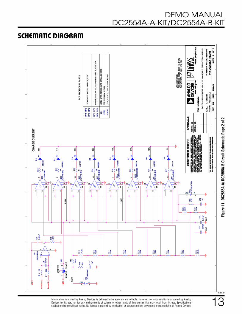
Figu
re 1
1. D
C255
5A-A
/ DC2
555A
-B C
ircui
t Sch
emat
ic P
age
2 of
2
14
DEMO MANUAL DC2554A-A-KIT/DC2554A-B-KIT
Rev. 0
ANALOG DEVICES, INC. 2019
12/19www.analog.com
ESD Caution ESD (electrostatic discharge) sensitive device. Charged devices and circuit boards can discharge without detection. Although this product features patented or proprietary protection circuitry, damage may occur on devices subjected to high energy ESD. Therefore, proper ESD precautions should be taken to avoid performance degradation or loss of functionality.
Legal Terms and Conditions By using the evaluation board discussed herein (together with any tools, components documentation or support materials, the “Evaluation Board”), you are agreeing to be bound by the terms and conditions set forth below (“Agreement”) unless you have purchased the Evaluation Board, in which case the Analog Devices Standard Terms and Conditions of Sale shall govern. Do not use the Evaluation Board until you have read and agreed to the Agreement. Your use of the Evaluation Board shall signify your acceptance of the Agreement. This Agreement is made by and between you (“Customer”) and Analog Devices, Inc. (“ADI”), with its principal place of business at One Technology Way, Norwood, MA 02062, USA. Subject to the terms and conditions of the Agreement, ADI hereby grants to Customer a free, limited, personal, temporary, non-exclusive, non-sublicensable, non-transferable license to use the Evaluation Board FOR EVALUATION PURPOSES ONLY. Customer understands and agrees that the Evaluation Board is provided for the sole and exclusive purpose referenced above, and agrees not to use the Evaluation Board for any other purpose. Furthermore, the license granted is expressly made subject to the following additional limitations: Customer shall not (i) rent, lease, display, sell, transfer, assign, sublicense, or distribute the Evaluation Board; and (ii) permit any Third Party to access the Evaluation Board. As used herein, the term “Third Party” includes any entity other than ADI, Customer, their employees, affiliates and in-house consultants. The Evaluation Board is NOT sold to Customer; all rights not expressly granted herein, including ownership of the Evaluation Board, are reserved by ADI. CONFIDENTIALITY. This Agreement and the Evaluation Board shall all be considered the confidential and proprietary information of ADI. Customer may not disclose or transfer any portion of the Evaluation Board to any other party for any reason. Upon discontinuation of use of the Evaluation Board or termination of this Agreement, Customer agrees to promptly return the Evaluation Board to ADI. ADDITIONAL RESTRICTIONS. Customer may not disassemble, decompile or reverse engineer chips on the Evaluation Board. Customer shall inform ADI of any occurred damages or any modifications or alterations it makes to the Evaluation Board, including but not limited to soldering or any other activity that affects the material content of the Evaluation Board. Modifications to the Evaluation Board must comply with applicable law, including but not limited to the RoHS Directive. TERMINATION. ADI may terminate this Agreement at any time upon giving written notice to Customer. Customer agrees to return to ADI the Evaluation Board at that time. LIMITATION OF LIABILITY. THE EVALUATION BOARD PROVIDED HEREUNDER IS PROVIDED “AS IS” AND ADI MAKES NO WARRANTIES OR REPRESENTATIONS OF ANY KIND WITH RESPECT TO IT. ADI SPECIFICALLY DISCLAIMS ANY REPRESENTATIONS, ENDORSEMENTS, GUARANTEES, OR WARRANTIES, EXPRESS OR IMPLIED, RELATED TO THE EVALUATION BOARD INCLUDING, BUT NOT LIMITED TO, THE IMPLIED WARRANTY OF MERCHANTABILITY, TITLE, FITNESS FOR A PARTICULAR PURPOSE OR NONINFRINGEMENT OF INTELLECTUAL PROPERTY RIGHTS. IN NO EVENT WILL ADI AND ITS LICENSORS BE LIABLE FOR ANY INCIDENTAL, SPECIAL, INDIRECT, OR CONSEQUENTIAL DAMAGES RESULTING FROM CUSTOMER’S POSSESSION OR USE OF THE EVALUATION BOARD, INCLUDING BUT NOT LIMITED TO LOST PROFITS, DELAY COSTS, LABOR COSTS OR LOSS OF GOODWILL. ADI’S TOTAL LIABILITY FROM ANY AND ALL CAUSES SHALL BE LIMITED TO THE AMOUNT OF ONE HUNDRED US DOLLARS ($100.00). EXPORT. Customer agrees that it will not directly or indirectly export the Evaluation Board to another country, and that it will comply with all applicable United States federal laws and regulations relating to exports. GOVERNING LAW. This Agreement shall be governed by and construed in accordance with the substantive laws of the Commonwealth of Massachusetts (excluding conflict of law rules). Any legal action regarding this Agreement will be heard in the state or federal courts having jurisdiction in Suffolk County, Massachusetts, and Customer hereby submits to the personal jurisdiction and venue of such courts. The United Nations Convention on Contracts for the International Sale of Goods shall not apply to this Agreement and is expressly disclaimed.