Embed Size (px)
DESCRIPTION
Continuous-Time Laser Programmable Analog Array for Radiation Environments. MAPLD September 8 – 10 2004. Anthony L. Wilson ATK Mission Research 5001 Indian School Road NE Albuquerque, NM [email protected]. Ji Luo, Joseph B. Bernstein, J. Ari Tuchman, Hu Huang, Kuan-Jung Chung - PowerPoint PPT Presentation
Citation preview
Continuous-Time Laser Programmable Continuous-Time Laser Programmable Analog Array for Radiation EnvironmentsAnalog Array for Radiation Environments
Anthony L. Wilson
ATK Mission Research5001 Indian School Road NEAlbuquerque, [email protected]
MAPLDSeptember 8 – 10 2004
Ji Luo, Joseph B. Bernstein, J. Ari Tuchman, Hu Huang, Kuan-Jung Chung
University of Maryland2100 Marie Mount HallCollege Park, MD
Wilson B117/MAPLD 20042
OutlineOutline
• Introduction – Goals and Objectives
• Overview of Technical Approach
• Process Description
• “Switch” Description
• Amplifier Design
• Configurable Analog Block (CAB) Architecture
• Laser Programmable Analog Array (LPAA) Architecture Description
• How to get from Point A to Point B - Router Development
• User Interface
• Lessons Learned
Wilson B117/MAPLD 20043
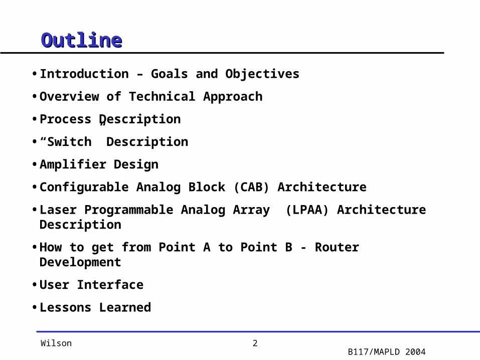
IntroductionIntroduction
• Definitions• LPAA: Laser-Programmable Analog Array• CAB: Configurable Analog Array• FBFTFN: Fully Balanced Four-Terminal Floating Nullor• PRA: Programmable Resistor Array• PCA: Programmable Capacitor Array• SOS: Silicon-on-Sapphire
“… a monolithic collection of analog building blocks, a user-controllable routing network used for passing signals between building blocks…”
E. Pierzchala, et al., “Field-Programmable Analog Arrays”, Kluwer Academic Pub., 1998
Wilson B117/MAPLD 20044
Goals/ObjectivesGoals/Objectives
• Design of a radiation tolerant programmable analog array
• Design of an high performance analog array
• Demonstration of the laser via technology
• Demonstration of Peregrine UTSi™ CMOS SOS technology for analog applications
• Development of an analog router for analog arrays
Wilson B117/MAPLD 20045
Overview of LPAA DesignOverview of LPAA Design
• Array style architecture
• Fully Differential Circuit Topology
• Voltage and Current Mode Capability
• CMOS Silicon-on-Sapphire Technology
• Continuous-Time Operation
• Parasitic Aware Analog Router
• Low Resistant Laser Via Technology
Wilson B117/MAPLD 20046
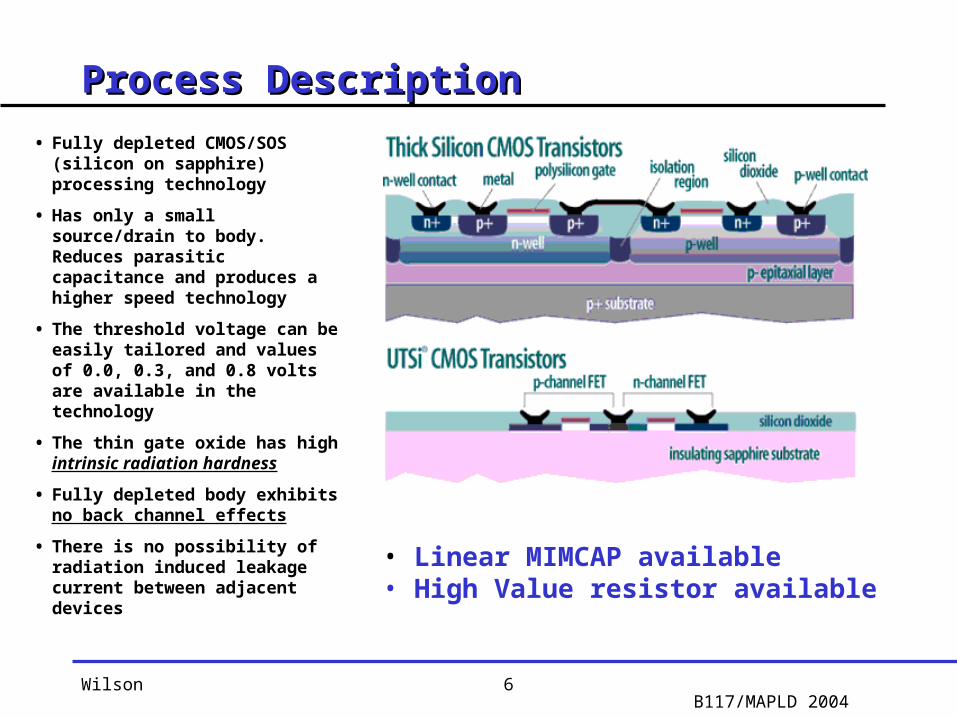
Process DescriptionProcess Description• Fully depleted CMOS/SOS
(silicon on sapphire) processing technology
• Has only a small source/drain to body. Reduces parasitic capacitance and produces a higher speed technology
• The threshold voltage can be easily tailored and values of 0.0, 0.3, and 0.8 volts are available in the technology
• The thin gate oxide has high intrinsic radiation hardness
• Fully depleted body exhibits no back channel effects
• There is no possibility of radiation induced leakage current between adjacent devices
• Linear MIMCAP available• High Value resistor available
Wilson B117/MAPLD 20047
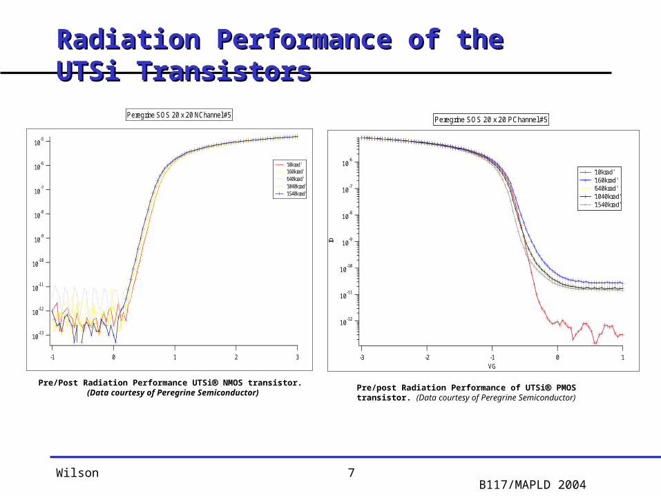
Radiation Performance of the UTSi TransistorsRadiation Performance of the UTSi Transistors
Pre/Post Radiation Performance UTSi NMOS transistor. (Data courtesy of Peregrine Semiconductor) Pre/post Radiation Performance of UTSi PMOS transistor. (Data
courtesy of Peregrine Semiconductor)
10-13
10-12
10-11
10-10
10-9
10-8
10-7
10-6
10-5
3210-1
'10krad' '160krad' '640krad' '1040krad' '1540krad'
Peregrine SOS 20 x 20 NChannel #5
10-12
10-11
10-10
10-9
10-8
10-7
10-6
ID
-3 -2 -1 0 1VG
'10krad' '160krad' '640krad' '1040krad' '1540krad'
Peregrine SOS 20 x 20 PChannel #5
Wilson B117/MAPLD 20048
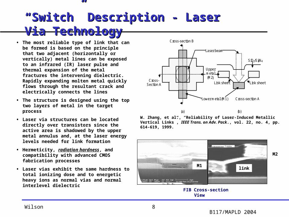
““Switch” Description - Laser Via TechnologySwitch” Description - Laser Via Technology• The most reliable type of link that can be
formed is based on the principle that two adjacent (horizontally or vertically) metal lines can be exposed to an infrared (IR) laser pulse and thermal expansion of the metal fractures the intervening dielectric. Rapidly expanding molten metal quickly flows through the resultant crack and electrically connects the lines
• The structure is designed using the top two layers of metal in the target process
• Laser via structures can be located directly over transistors since the active area is shadowed by the upper metal annulus and, at the laser energy levels needed for link formation
• Hermeticity, radiation hardness, and compatibility with advanced CMOS fabrication processes
• Laser vias exhibit the same hardness to total ionizing dose and to energetic heavy ions as normal vias and normal interlevel dielectric
Lower metal (M1)
Uppermetal(M2)
Laser beam
SiO2/Si3N4
Link sheetLink sheet
Cross-section B
Cross-Section A
Cross-section A
(a) (b)
linkM1
M2
FIB Cross-section View
W. Zhang, et al., “Reliability of Laser-Induced Metallic Vertical Links”, IEEE Trans. on Adv. Pack., vol. 22, no. 4, pp. 614-619, 1999.
Wilson B117/MAPLD 20049
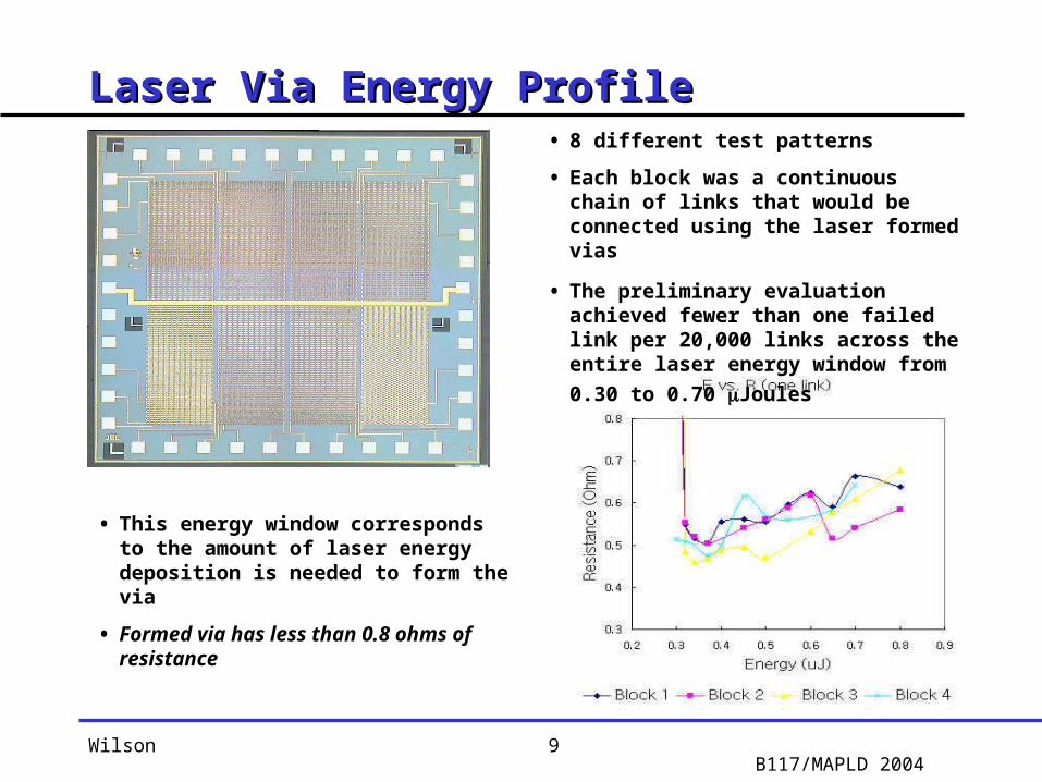
Laser Via Energy ProfileLaser Via Energy Profile
• This energy window corresponds to the amount of laser energy deposition is needed to form the via
• Formed via has less than 0.8 ohms of resistance
• 8 different test patterns
• Each block was a continuous chain of links that would be connected using the laser formed vias
• The preliminary evaluation achieved fewer than one failed link per 20,000 links across the entire laser energy window from 0.30 to 0.70 Joules

Wilson B117/MAPLD 200410
Amplifier DescriptionAmplifier Description• Fully balanced fully differential
architecture
• Fully Balanced Four-Terminal Floating Nullor (FBFTFN) Amplifier Structure
• Class AB output stage
•Differential difference input stage
•Inner and outer CMFB circuits (not shown)
•Bias circuit included (not shown)
•Provides voltage and current output nodes simultaneously
Wilson B117/MAPLD 200411
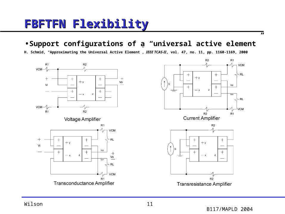
FBFTFN FlexibilityFBFTFN Flexibility
• Support configurations of a “universal active element”H. Schmid, “Approximating the Universal Active Element”, IEEE TCAS-II, vol. 47, no. 11, pp. 1160-1169, 2000
Wilson B117/MAPLD 200412
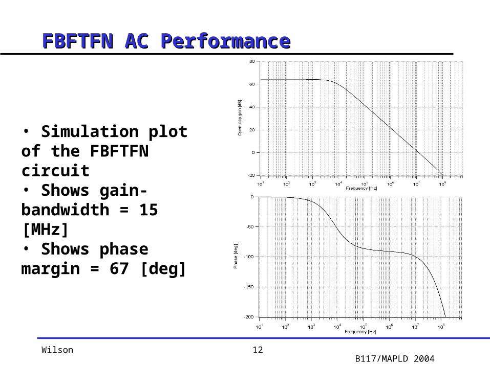
FBFTFN AC PerformanceFBFTFN AC Performance
• Simulation plot of the FBFTFN circuit• Shows gain-bandwidth = 15 [MHz]• Shows phase margin = 67 [deg]
Wilson B117/MAPLD 200413
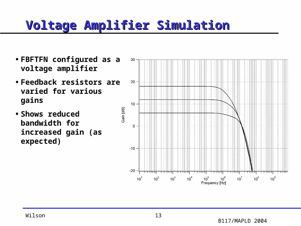
Voltage Amplifier SimulationVoltage Amplifier Simulation
• FBFTFN configured as a voltage amplifier
• Feedback resistors are varied for various gains
• Shows reduced bandwidth for increased gain (as expected)
Wilson B117/MAPLD 200414
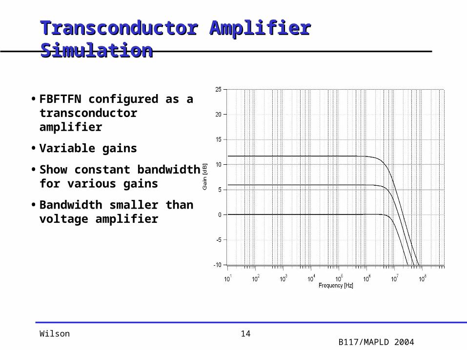
Transconductor Amplifier SimulationTransconductor Amplifier Simulation
• FBFTFN configured as a transconductor amplifier
• Variable gains
• Show constant bandwidth for various gains
• Bandwidth smaller than voltage amplifier
Wilson B117/MAPLD 200415
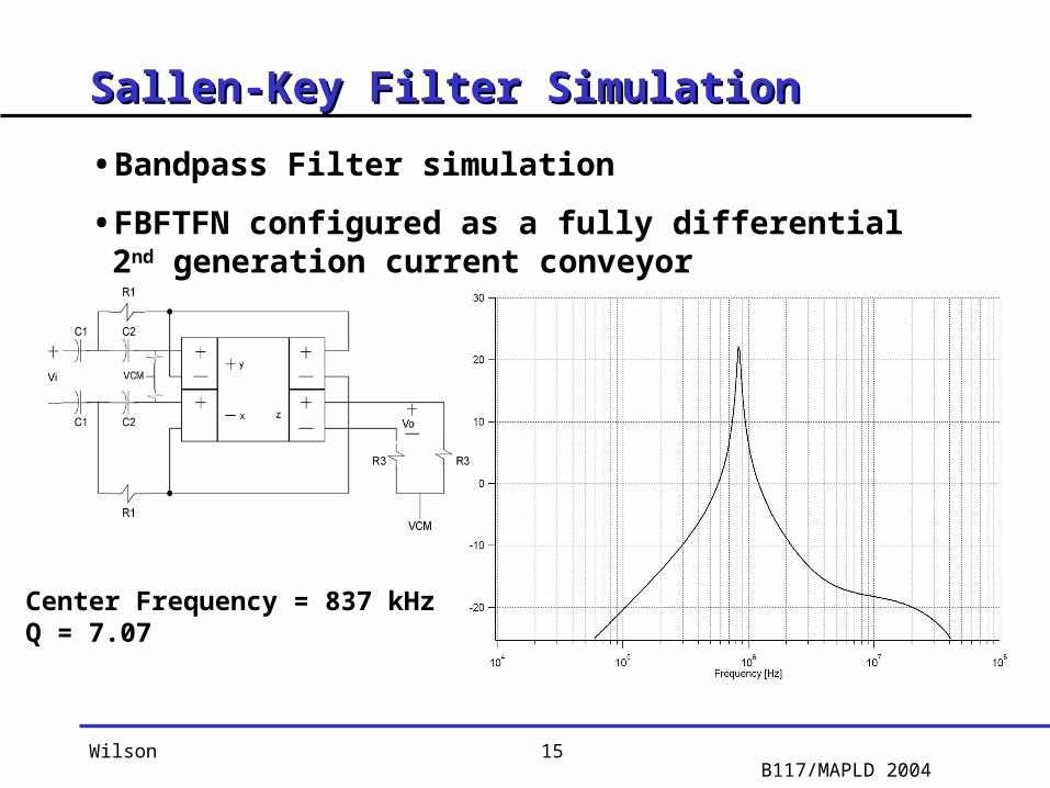
Sallen-Key Filter SimulationSallen-Key Filter Simulation
• Bandpass Filter simulation
• FBFTFN configured as a fully differential 2nd generation current conveyor
Center Frequency = 837 kHz Q = 7.07
Wilson B117/MAPLD 200416
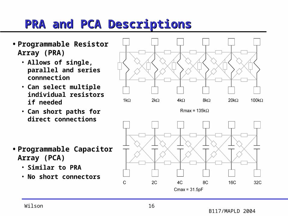
PRA and PCA DescriptionsPRA and PCA Descriptions• Programmable Resistor
Array (PRA)• Allows of single, parallel
and series connnection• Can select multiple
individual resistors if needed
• Can short paths for direct connections
• Programmable Capacitor Array (PCA)• Similar to PRA• No short connectors
Wilson B117/MAPLD 200417
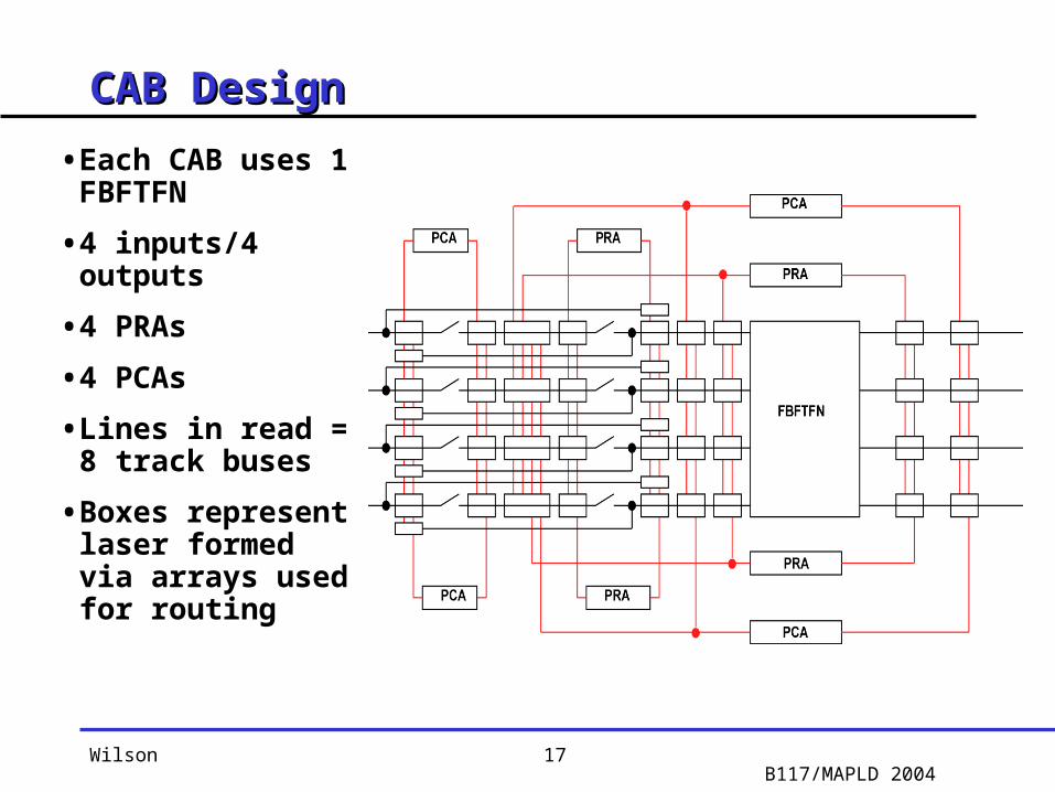
CAB DesignCAB Design
• Each CAB uses 1 FBFTFN
• 4 inputs/4 outputs
• 4 PRAs
• 4 PCAs
• Lines in read = 8 track buses
• Boxes represent laser formed via arrays used for routing
Wilson B117/MAPLD 200418
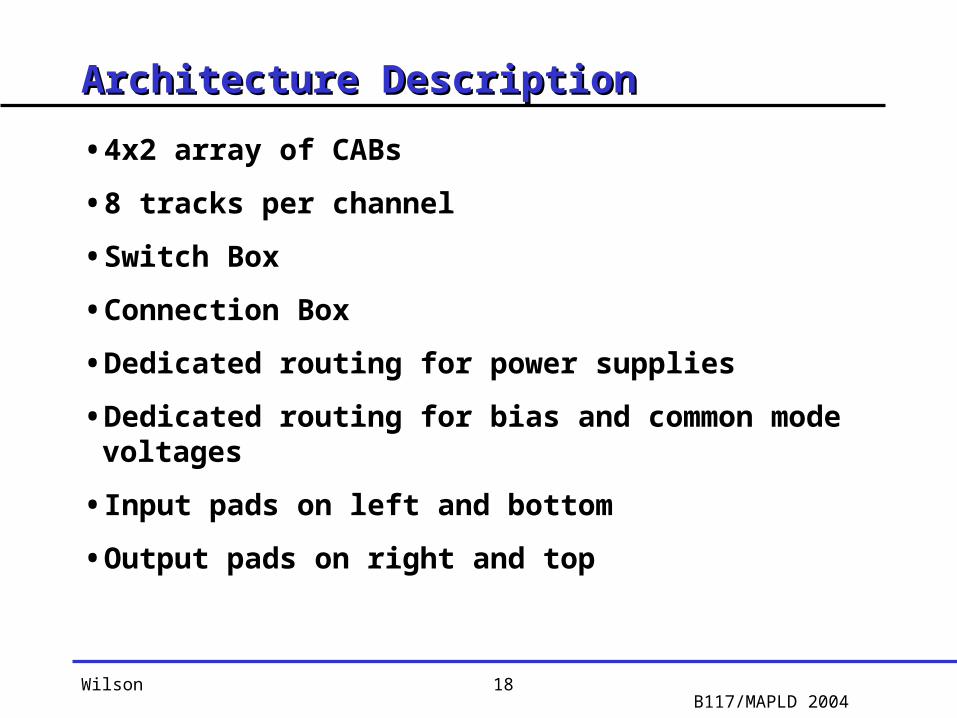
Architecture DescriptionArchitecture Description
• 4x2 array of CABs
• 8 tracks per channel
• Switch Box
• Connection Box
• Dedicated routing for power supplies
• Dedicated routing for bias and common mode voltages
• Input pads on left and bottom
• Output pads on right and top
Wilson B117/MAPLD 200419
Analog Array Architecture DescriptionAnalog Array Architecture Description
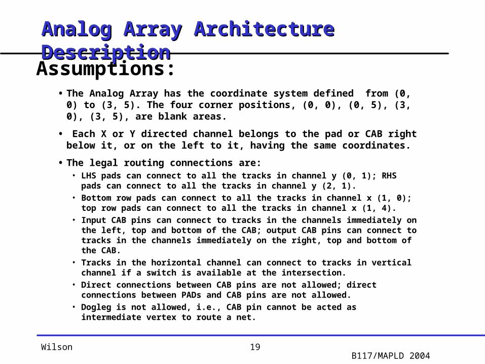
• The Analog Array has the coordinate system defined from (0, 0) to (3, 5). The four corner positions, (0, 0), (0, 5), (3, 0), (3, 5), are blank areas.
• Each X or Y directed channel belongs to the pad or CAB right below it, or on the left to it, having the same coordinates.
• The legal routing connections are: • LHS pads can connect to all the tracks in channel y (0, 1); RHS pads can connect
to all the tracks in channel y (2, 1).• Bottom row pads can connect to all the tracks in channel x (1, 0); top row pads can
connect to all the tracks in channel x (1, 4).• Input CAB pins can connect to tracks in the channels immediately on the left, top
and bottom of the CAB; output CAB pins can connect to tracks in the channels immediately on the right, top and bottom of the CAB.
• Tracks in the horizontal channel can connect to tracks in vertical channel if a switch is available at the intersection.
• Direct connections between CAB pins are not allowed; direct connections between PADs and CAB pins are not allowed.
• Dogleg is not allowed, i.e., CAB pin cannot be acted as intermediate vertex to route a net.
Assumptions:
Wilson B117/MAPLD 200420
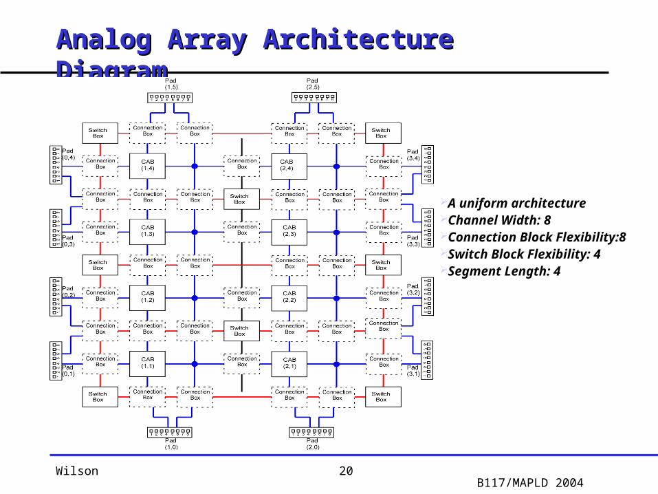
Analog Array Architecture DiagramAnalog Array Architecture Diagram
A uniform architectureChannel Width: 8Connection Block Flexibility:8Switch Block Flexibility: 4Segment Length: 4
Wilson B117/MAPLD 200421
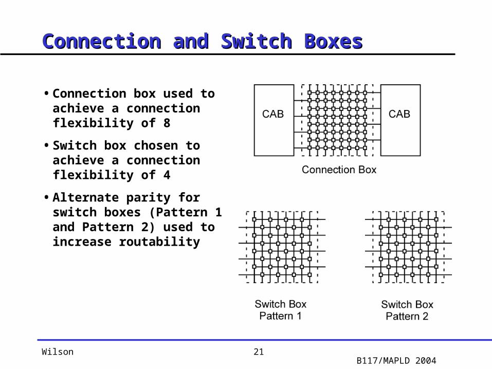
Connection and Switch BoxesConnection and Switch Boxes
• Connection box used to achieve a connection flexibility of 8
• Switch box chosen to achieve a connection flexibility of 4
• Alternate parity for switch boxes (Pattern 1 and Pattern 2) used to increase routability
Wilson B117/MAPLD 200422
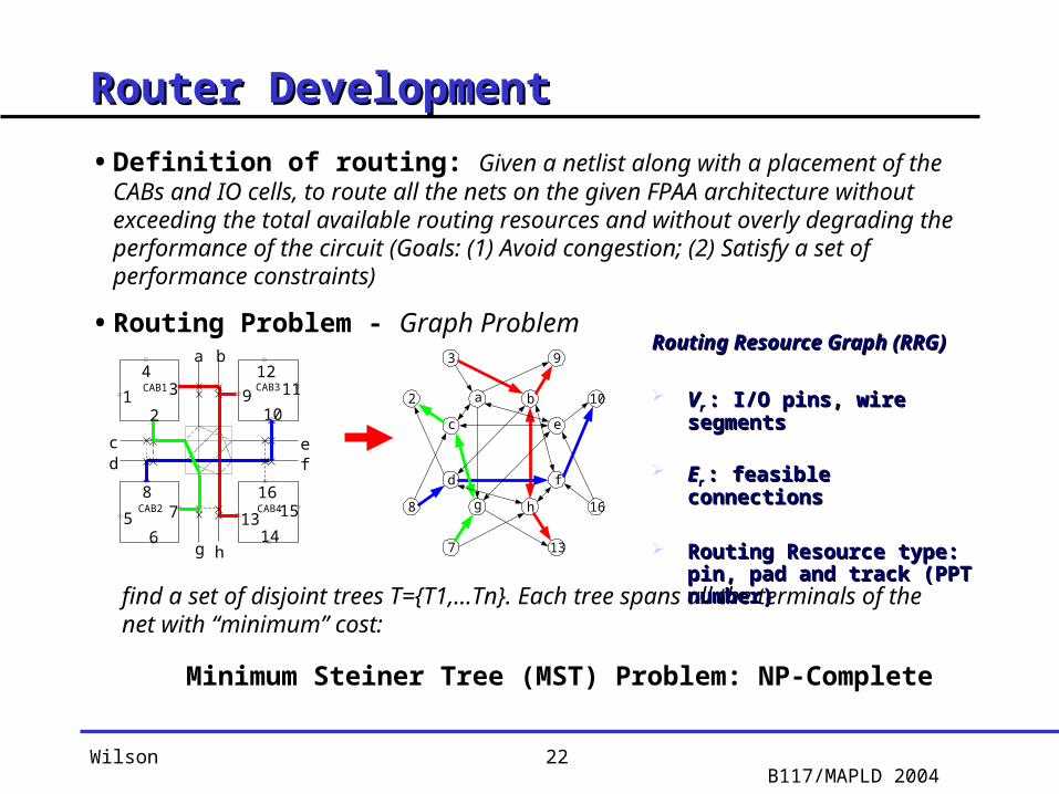
Router DevelopmentRouter Development• Definition of routing: Given a netlist along with a placement of the CABs and IO
cells, to route all the nets on the given FPAA architecture without exceeding the total available routing resources and without overly degrading the performance of the circuit (Goals: (1) Avoid congestion; (2) Satisfy a set of performance constraints)
• Routing Problem - Graph Problem
3
2
8
7 13
16
10
9
a b
c
d
g h
e
f
a b
cd
ef
g h
12
34
56
78
910
1314
1112
1516
CAB1
CAB2
CAB3
CAB4
find a set of disjoint trees T={T1,…Tn}. Each tree spans all the terminals of the net with “minimum” cost:
Minimum Steiner Tree (MST) Problem: NP-Complete
Routing Resource Graph (RRG)Routing Resource Graph (RRG)
VVr r : I/O pins, wire segments: I/O pins, wire segments
EEr r : feasible connections : feasible connections
Routing Resource type: pin, Routing Resource type: pin, pad and track (PPT number)pad and track (PPT number)
Wilson B117/MAPLD 200423
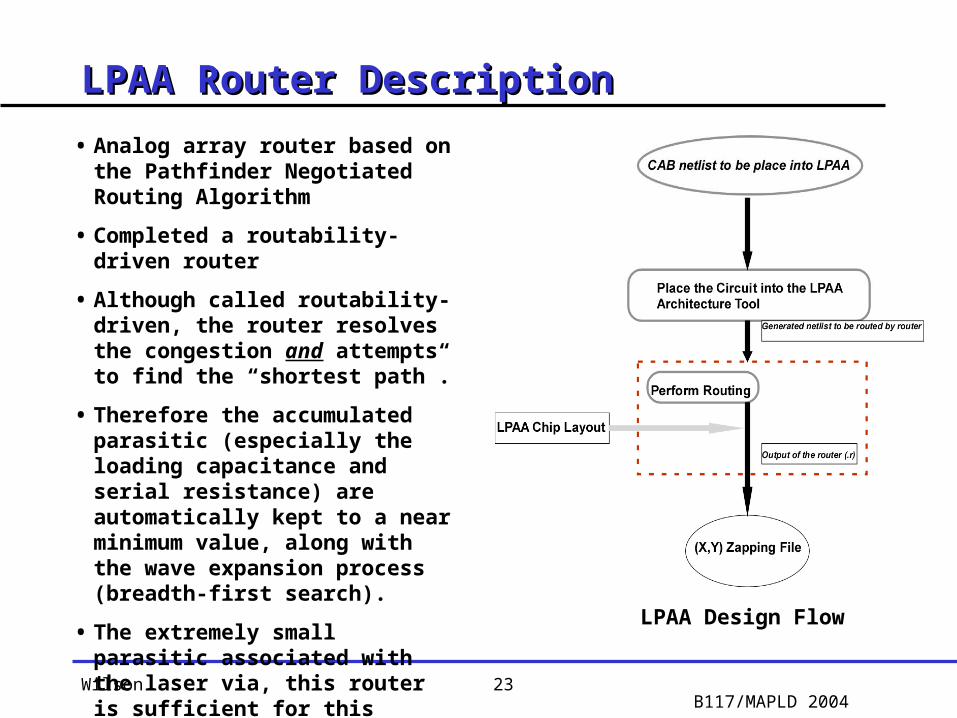
LPAA Router DescriptionLPAA Router Description• Analog array router based on the
Pathfinder Negotiated Routing Algorithm
• Completed a routability-driven router
• Although called routability-driven, the router resolves the congestion and attempts to find the “shortest path”.
• Therefore the accumulated parasitic (especially the loading capacitance and serial resistance) are automatically kept to a near minimum value, along with the wave expansion process (breadth-first search).
• The extremely small parasitic associated with the laser via, this router is sufficient for this relatively small-scaled analog array LPAA Design Flow
Wilson B117/MAPLD 200424
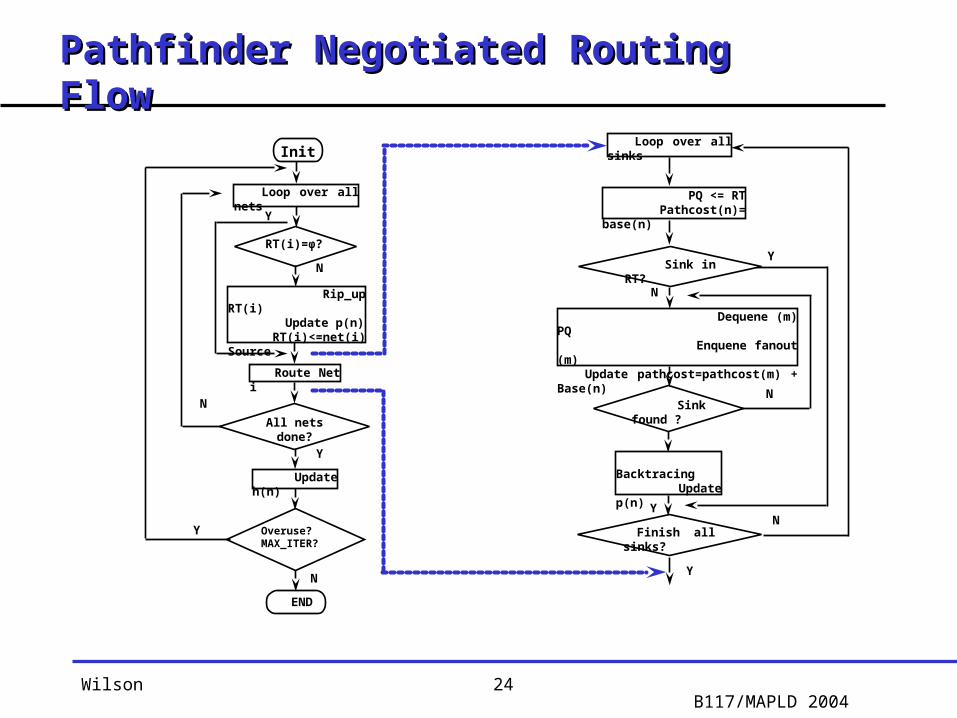
Pathfinder Negotiated Routing FlowPathfinder Negotiated Routing Flow
Route Net i
Init
Loop over all nets
RT(i)=φ?
Rip_up RT(i) Update p(n) RT(i)<=net(i) Source
All nets done?
Update h(n)
Overuse? MAX_ITER?
END
N
N
N
Y
Y
Sink in RT?
Dequene (m) PQ Enquene fanout (m) Update pathcost=pathcost(m) + Base(n)
Finish all sinks?
N
N
PQ <= RT Pathcost(n)= base(n)
Sink found ?
Backtracing Update p(n)
Loop over all sinks
N
Y
Y
Y
Y

Wilson B117/MAPLD 200425
User InterfaceUser Interface
• JavaTM chosen as language – cross platform
• Direct input from user
• Allows user to perform local connections within CAB
• Allows user to perform CAB-to-CAB connections
• Spice netlist creation
• Router compatible netlist file creation
Wilson B117/MAPLD 200426
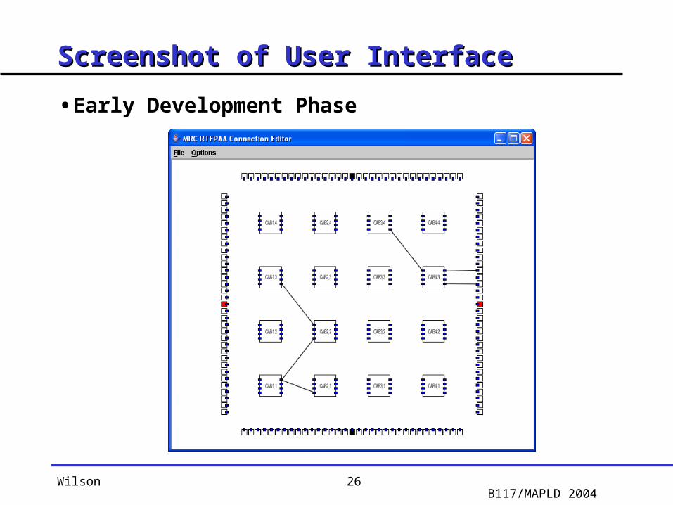
Screenshot of User InterfaceScreenshot of User Interface
• Early Development Phase
Wilson B117/MAPLD 200427
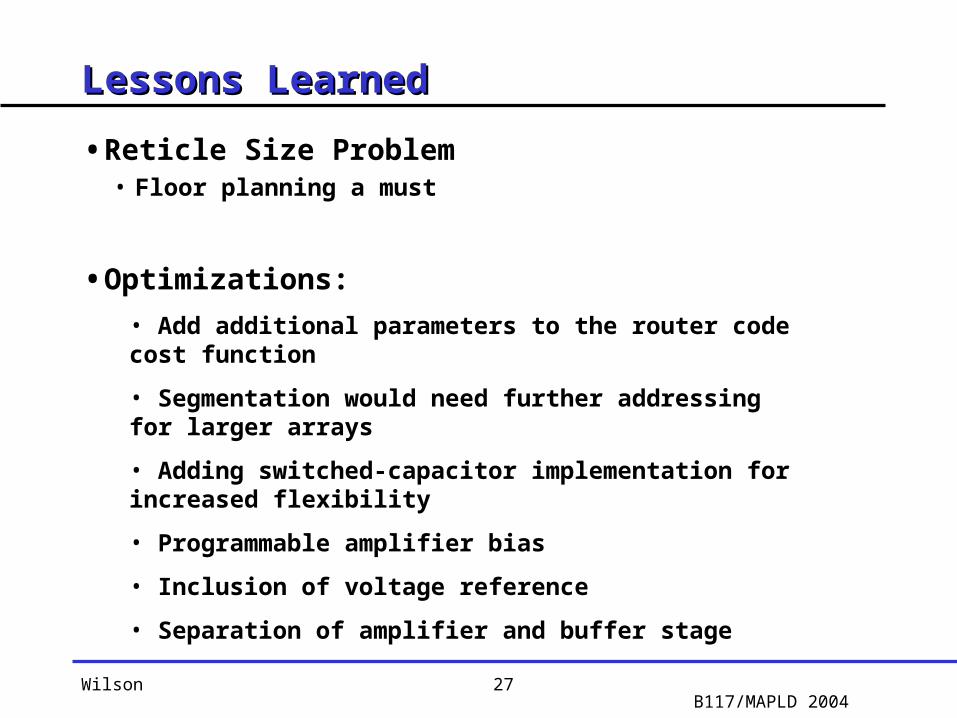
Lessons LearnedLessons Learned
• Reticle Size Problem• Floor planning a must
•Optimizations:• Add additional parameters to the router code cost function
• Segmentation would need further addressing for larger arrays
• Adding switched-capacitor implementation for increased flexibility
• Programmable amplifier bias
• Inclusion of voltage reference
• Separation of amplifier and buffer stage